

Texas Instruments 5962-9235001MXA Datasheet
L293
QUADRUPLE HALF-H DRIVER
SLRS005 – SEPTEMBER 1986 – REVISED MAY 1990
Copyright 1990, Texas Instruments Incorporated
3–1
POST OFFICE BOX 655303 • DALLAS, TEXAS 75265
• 1-A Output Current Capability Per Driver
• Pulsed Current 2-A Driver
• Wide Supply Voltage Range: 4.5 V to 36 V
• Separate Input-Logic Supply
• NE Package Designed for Heat Sinking
• Thermal Shutdown
• Internal ESD Protection
• High-Noise-Immunity Inputs
• Functional Replacement for SGS L293
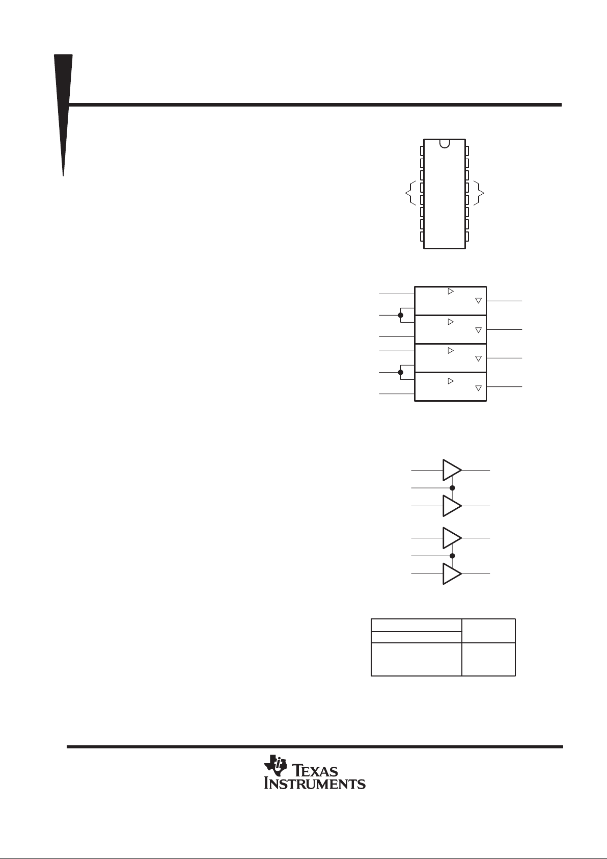
description
The L293 is a quadruple high-current half-H driver
designed to provide bidirectional drive currents of
up to 1 A at voltages from 4.5 V to 36 V. It is
designed to drive inductive loads such as relays,
solenoids, dc and bipolar stepping motors, as well
as other high-current/high-voltage loads in
positive-supply applications.
All inputs are TTL compatible. Each output is a
complete totem-pole drive circuit with a Darlington
transistor sink and a pseudo-Darlington source.
Drivers are enabled in pairs with drivers 1 and 2
enabled by 1,2EN and drivers 3 and 4 enabled by
3,4EN. When an enable input is high, the
associated drivers are enabled and their outputs
are active and in phase with their inputs. When the
enable input is low, those drivers are disabled and
their outputs are off and in a high-impedance
state. With the proper data inputs, each pair of
drivers form a full-H (or bridge) reversible drive
suitable for solenoid or motor applications.
External high-speed output clamp diodes should
be used for inductive transient suppression. A
V
CC1
terminal, separate from V
CC2
, is provided for
the logic inputs to minimize device power
dissipation.
The L293 is designed for operation from 0°C
to 70°C.
1
2
3
4
5
6
7
8
16
15
14
13
12
11
10
9
1,2EN
1A
1Y
2Y
2A
V
CC2
V
CC1
4A
4Y
3Y
3A
3,4EN
NE PACKAGE
(TOP VIEW)
HEAT SINK AND
GROUND
HEAT SINK AND
GROUND
logic symbol
†
4A
3,4EN
3A
2A
1,2EN
1A
15
9
10
7
1
2
4Y
3Y
2Y
1Y
14
11
6
3
EN
EN
EN
EN
†
This symbol is in accordance with ANSI/IEEE Std 91-1984 and
IEC publication 617-12.
logic diagram
4A
3,4EN
3A
2A
1,2EN
1A
15
9
10
7
1
2
4Y
3Y
2Y
1Y
14
11
6
3
INPUTS
‡
OUTPUT
Y
H
L
X
FUNCTION TABLE
(each driver)
AEN
H
H
L
H
L
Z
H = high-level, L = low-level,
X = irrelevant, Z = high-impedance (off)
‡
In the thermal shutdown mode, the
output is in the high-impedance state
regardless of the input levels.
PRODUCTION DATA information is current as of publication date.
Products conform to specifications per the terms of Texas Instruments
standard warranty. Production processing does not necessarily include
testing of all parameters.
L293
QUADRUPLE HALF-H DRIVER
SLRS005 – SEPTEMBER 1986 – REVISED MAY 1990
3–2
POST OFFICE BOX 655303 • DALLAS, TEXAS 75265
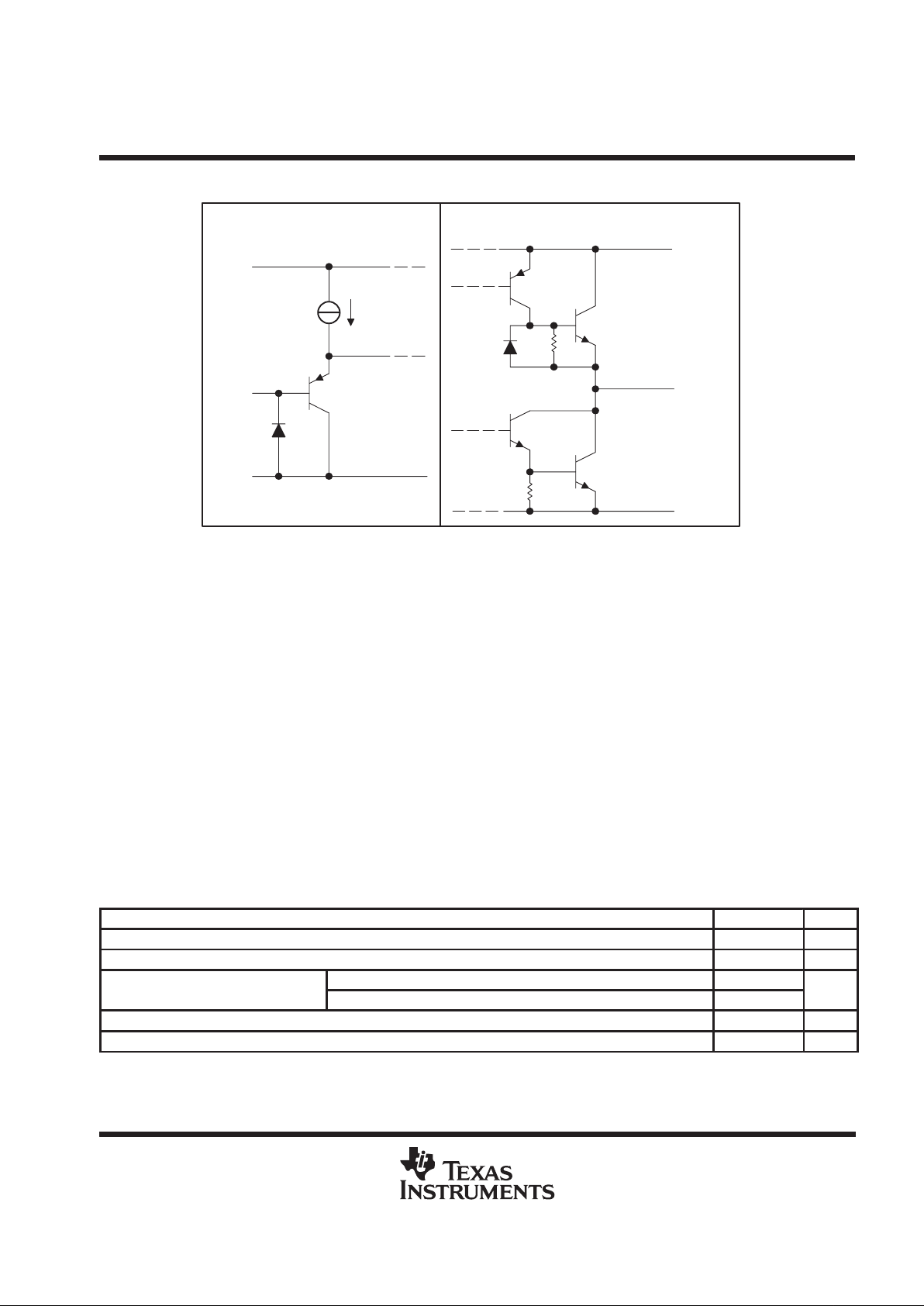
schematics of inputs and outputs
Input
V
CC2
Output
GND
TYPICAL OF ALL OUTPUTS
EQUIVALENT OF EACH INPUT
V
CC1
Current
Source
GND
absolute maximum ratings over operating free-air temperature range (unless otherwise noted)
Supply voltage, V
CC1
(see Note 1) 36 V. . . . . . . . . . . . . . . . . . . . . . . . . . . . . . . . . . . . . . . . . . . . . . . . . . . . . . . . . .
Output supply voltage range, V
CC2
36 V. . . . . . . . . . . . . . . . . . . . . . . . . . . . . . . . . . . . . . . . . . . . . . . . . . . . . . . . . .
Input voltage range, VI 7 V. . . . . . . . . . . . . . . . . . . . . . . . . . . . . . . . . . . . . . . . . . . . . . . . . . . . . . . . . . . . . . . . . . . . . . .
Output voltage range, VO –3 V to V
CC2
+ 3 V. . . . . . . . . . . . . . . . . . . . . . . . . . . . . . . . . . . . . . . . . . . . . . . . . . . . .
Peak output current, IO (nonrepetitive, t ≤ 5 ms) ±2 A. . . . . . . . . . . . . . . . . . . . . . . . . . . . . . . . . . . . . . . . . . . . . .
Continuous output current, I
O
±1 A. . . . . . . . . . . . . . . . . . . . . . . . . . . . . . . . . . . . . . . . . . . . . . . . . . . . . . . . . . . . . . .
Continuous total dissipation at (or below) 25°C free-air temperature (see Notes 2 and 3) 2075 mW. . . . . . .
Continuous total dissipation at 80°C case temperature (see Note 3) 5000 mW. . . . . . . . . . . . . . . . . . . . . . . . .
Operating case or virtual junction temperature range, TA –40°C to 150°C. . . . . . . . . . . . . . . . . . . . . . . . . . . . .
Storage temperature range, T
stg
–65°C to 150°C. . . . . . . . . . . . . . . . . . . . . . . . . . . . . . . . . . . . . . . . . . . . . . . . . .
Lead temperature 1,6 mm (1/16 inch) from case for 10 seconds 260°C. . . . . . . . . . . . . . . . . . . . . . . . . . . . . . .
NOTES: 1. All voltage values are with respect to the network ground terminal.
2. For operation above 25°C free-air temperature, derate linearly at the rate of 16.6 mW/°C.
3. For operation above 25°C case temperature, derate linearly at the rate of 71.4 mW/°C. Due to variations in individual device electrical
characteristics and thermal resistance, the built-in thermal overload protection may be activated at power levels slightly above or
below the rated dissipation.
recommended operating conditions
MIN MAX UNIT
Logic supply voltage, V
CC1
4.5 7 V
Output supply voltage, V
CC2
36 V
p
V
CC1
≤ 7 V 2.3
High-level input voltage, V
IH
V
CC1
≥ 7 V 2.3 7
V
Low-level output voltage, V
IL
–0.3
†
1.5 V
Operating free-air temperature, T
A
0 70 °C
†
The algebraic convention, in which the least positive (most negative) designated minimum, is used in this data sheet for logic voltage levels.
 Loading...