

Texas Instruments CY74FCT646ATSOCT, CY74FCT646ATSOC, CY74FCT646ATQCT, CY74FCT646ATQC, CY74FCT646TSOCT Datasheet
...
8-Bit Registered Transceive
r
CY54/74FCT646T
SCCS031 - July 1994 - Revised March 2000
Data sheet acquired from Cypress Semiconductor Corporation.
Data sheet modified to remove devices not offered.
Copyright © 2000, Texas Instruments Incorporated
Features
• Function, pinout, and drive compatible with FCT and
F logic
• FCT-C speed at 5.4 ns max. (Com’l)
FCT-A speed at 6.3 ns max. (Com’l)
• Reduced V
OH
(typically = 3.3V) versions of equivalent
FCT functions
• Edge-rate control circuitry for significantly improved
noise characteristics
• Power-off disable feature permits live insertion
• Matched rise and fall times
• Fully compatible with TTL input and output logic levels
• ESD > 2000V
• Sink current 64 mA (Com’l), 48 mA (Mil)
Source current 32 mA (Com’l), 12 mA (Mil)
• Independent register for A and B buses
• Extended commercial range of −40˚C to +85˚C
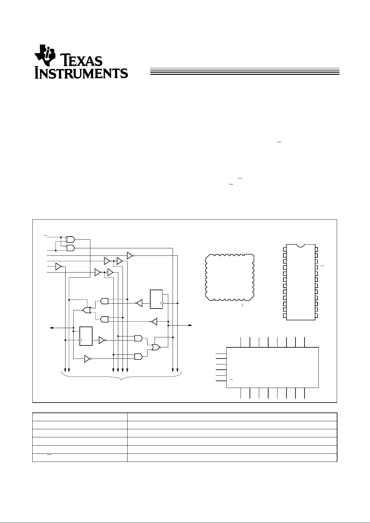
Functional Description
The FCT646T consists of a bus transceiver circuit with
three-state, D-type flip-flops, and control circuitry arranged for
multiplexedtransmission of data directly from the input bus or
from the internal registers. Data on the A or B bus will be
clocked into the registers as the appropriate clock pin goes to
a HIGH logic level. Enable Control
G and direction pins are
provided to control the transceiver function. In the transceiver
mode, data present at the high-impedance port may be stored
in either the A or B register, or in both. The select controls can
multiplex stored and real-time (transparent mode) data. The
direction control determines which bus will receive data when
the enable control
G is Active LOW. In the isolation mode
(enable Control
G HIGH), A data may be stored in the B reg-
ister and/or B data may be stored in the A register.
The outputs of the FCT646T are designed with a power-off
disable feature to allo w for liv e insertion of boards.
Logic Block Diagram
Pin Configurations
C
D
B
1
28
4
5678910
3
2
1
27
13
14
15
16
17
26
2524232221
20
11
12
19
A
3
A5A
4
B
2
B
5
18
B
1
NC
NC
B
4
A
2
LCC
Top View
B
3
C
D
A
1
TO 7 OTHER CHANNELS
SAB
CPAB
CPBA
DIR
SBA
G
V
CC
CPAB
A
7
A
8
B
6
B
7
B
8
CPBA
SAB
SBA
DIR
A
6
A
1
G
NC
NC
GND
Function Block Diagrams
1
2
3
4
5
6
7
8
9
10
11
12
16
17
18
19
20
24
23
22
21
13
14
V
CC
15
QSOP, SOIC
Top View
CPAB
A
1
A
2
A
3
A
4
A
5
A
6
A
7
A
8
B
1
B
2
B
3
B
4
B
5
B
6
B
7
B
8
CPBA
SAB
SBADIR
G
GND
CPAB
A
1A2A3A4A5A6A7A8
B1B2B3B4B5B6B7B
8
CPBA
SAB
SBA
DIR
G
Pin Description
Name Description
A Data Register A Inputs, Data Register B Outputs
B Data Register B Inputs, Data Register A Outputs
CPAB, CPBA Clock Pulse Inputs
SAB, SBA Output Data Source Select Inputs
DIR, G Output Enable Inputs
CY54/74FCT646T
2
BUS BBUS A
DIR
L
GLCPAB
X
CPBAXSABXSBA
L
BUS
BBUS A
DIR
H
L
X
G
L
L
H
CPAB
X
CPBAXSAB
X
X
X
SBA
X
X
X
BUS
BBUS A
DIR
H
GLCPAB
X
CPBAXSABLSBA
X
BUS
ABUS A
DIR
L
H
G
L
L
CPAB
X
HorL
CPBA
HorL
X
SAB
X
H
SBA
H
X
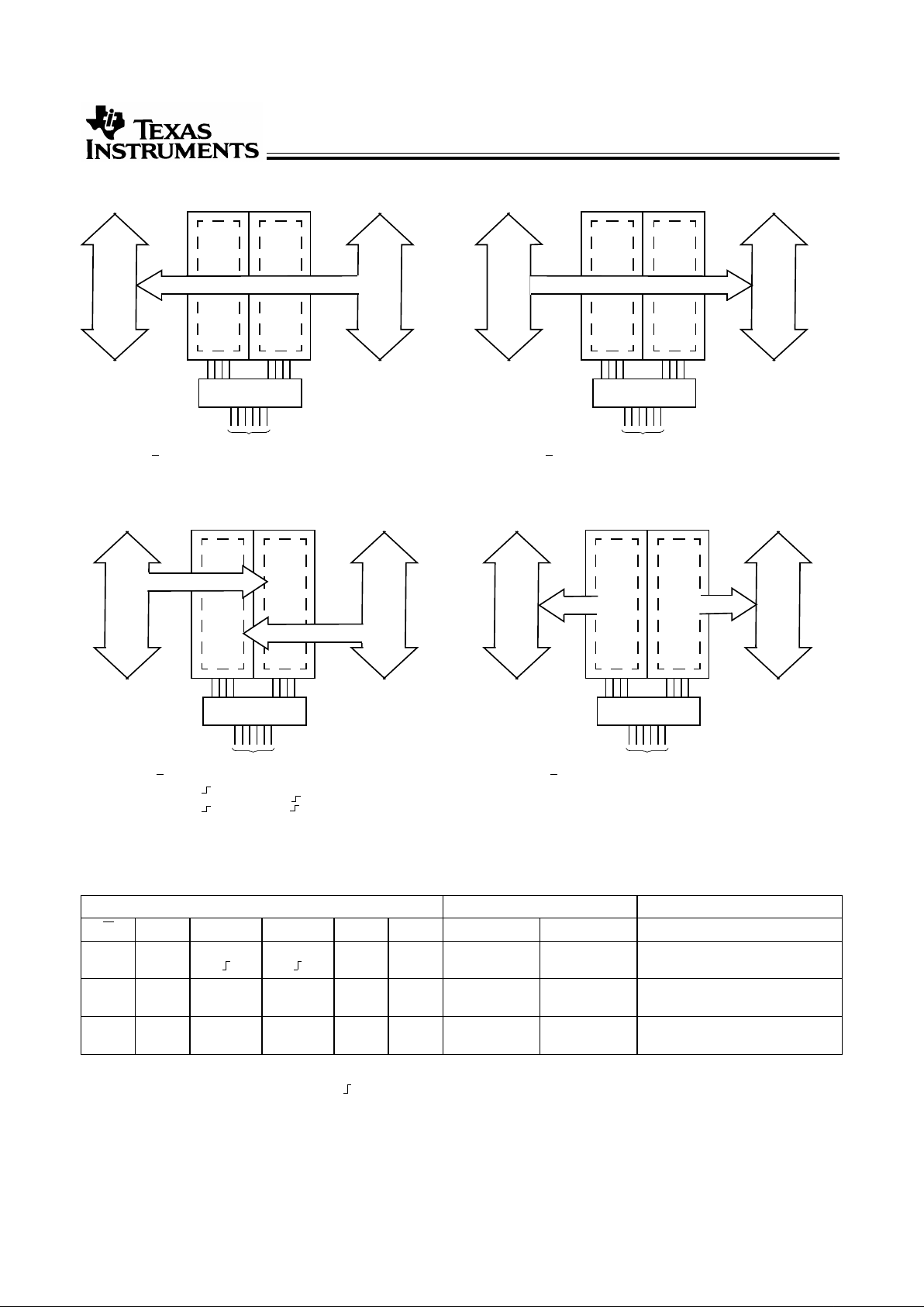
Real-Time Transfer
Bus B to Bus A
Real-Time Transfer
Bus A to Bus B
Storage from
A and/or B
Transfer Stored Data
to A and/or B
[1]
Function Table
[2]
Inputs Data I/O
[3]
Operation or Function
G DIR CPAB CPBA SAB SBA A1 thru A
8
B1 thru B
8
FCT646T
H
H
X
X
H or L H or L X
X
X
X
Input Input Isolation
Store A and B Data
L
L
L
L
X
X
X
H or L
X
X
L
H
Output Input Real Time B Data to A Bus
Stored B Data to A Bus
L
L
H
H
X
H or L
X
X
L
H
X
X
Input Output Real Time A Data to B Bus
Stored A Data to B Bus
Notes:
1. Cannot transfer data to A bus and B bus simultaneously.
2. H = HIGH Voltage Level, L = LOW Voltage Level, = LOW-to-HIGH Transition, X = Don’t Care.
3. The data outputfunctions may be enabledordisabled by various signalsat the G or DIR inputs.Data input functions are alwaysenabled, i.e., data atthe bus
pins will be stored on every LOW-to-HIGH transition of the clock inputs.
CY54/74FCT646T
3
Maximum Ratings
[4, 5]
(Above which the useful life may be impaired. For user
guidelines, not tested.)
Storage Temperature .................................–65°C to +150°C
Ambient Temperature with
Power Applied.............................................–65°C to +135°C
Supply Voltage to Ground Potential............... –0.5V to +7.0V
DC Input Voltage............................................–0.5V to +7.0V
DC Output Voltage......................................... –0.5V to +7.0V
DC Output Current (Maximum Sink Current/Pin).......120 mA
Power Dissipation..........................................................0.5W
Static Discharge Voltage............................................>2001V
(per MIL-STD-883, Method 3015)
Operating Range
Range Range
Ambient
Temperature V
CC
Commercial All –40°C to +85°C 5V ± 5%
Military
[6]
All –55°C to +125°C 5V ± 10%
Electrical Characteristics Over the Operating Range
Parameter Description Test Conditions Min. Typ.
[7]
Max. Unit
V
OH
Output HIGH Voltage VCC=Min., IOH=–32 mA Com’l 2.0 V
VCC=Min., IOH=–15 mA Com’l 2.4 3.3 V
VCC=Min., IOH=–12 mA Mil 2.4 3.3 V
V
OL
Output LOW Voltage VCC=Min., IOL=64 mA Com’l 0.3 0.55 V
VCC=Min., IOL=48 mA Mil 0.3 0.55 V
V
IH
Input HIGH Voltage 2.0 V
V
IL
Input LOW Voltage 0.8 V
V
H
Hysteresis
[8]
All inputs 0.2 V
V
IK
Input Clamp Diode Voltage VCC=Min., IIN=–18 mA –0.7 –1.2 V
I
I
Input HIGH Current VCC=Max., VIN=V
CC
5 µA
I
IH
Input HIGH Current
[8]
VCC=Max., VIN=2.7V ±1 µA
I
IL
Input LOW Current
[8]
VCC=Max., VIN=0.5V ±1 µA
I
OS
Output Short Circuit Current
[9]
VCC=Max., V
OUT
=0.0V –60 –120 –225 mA
I
OFF
Power-Off Disable VCC=0V, V
OUT
=4.5V ±1 µA
Capacitance
[8]
Parameter Description Typ.
[7]
Max. Unit
C
IN
Input Capacitance 6 10 pF
C
OUT
Output Capacitance 8 12 pF
Notes:
4. Unless otherwise noted, these limits are over the operating free-air temperature range.
5. Unused inputs must always be connected to an appropriate logic voltage level, preferably either V
CC
or ground.
6. TA is the “instant on” case temperature.
7. Typical values are at VCC=5.0V, TA=+25˚C ambient.
8. This parameter is specified but not tested.
9. Not morethanone output should beshorted ata time. Duration ofshort should notexceed one second.The use of high-speed testapparatus and/or sample
and hold techniques are preferable in order to minimize internal chip heating and more accurately reflect operational values. Otherwise prolonged shorting
of ahigh output mayraise thechiptemperature wellabove normal andthereby cause invalidreadings inother parametric tests.Inany sequenceof parameter
tests, IOS tests should be performed last.
 Loading...