Brushless DC Motor Controller
application
INFO
available
UC1625
UC2625
UC3625
FEATURES
Drives Power MOSFETs or Power Darlingtons
•
Directly
50V Open Collector High-Side Drivers
•
Latched Soft Start
•
High-speed Current-Sense Amplifier with Ideal
•
Diode
Pulse-by-Pulse and Average Current Sensing
•
Over-Voltage and Under-Voltage Protection
•
Direction Latch for Safe Direction Reversal
•
Tachometer
•
Trimmed Reference Sources 30mA
•
Programmable Cross-Conduction Protection
•
• Two-Quadrant and Four-Quadrant Operation
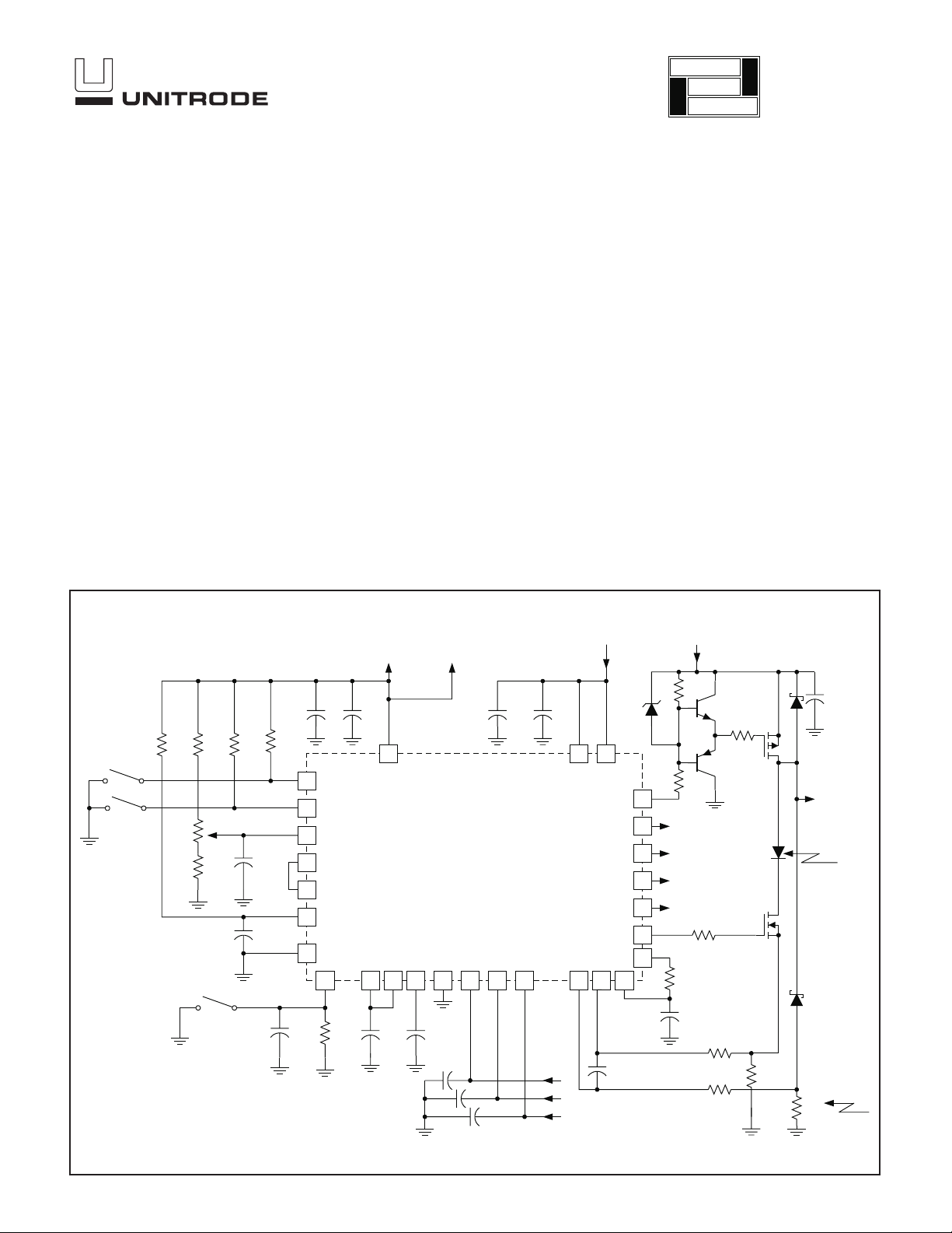
TYPICAL APPLICATION
DESCRIPTION
The UC3625 family of motor controller ICs integrate most of the
functions required for high-performance brushless DC motor con
trol into one package. When coupled with external power
MOSFETs or Darlingtons, these ICs perform fixed-frequency PWM
motor control in either voltage or current mode while implementing
closed loop speed control and braking with smart noise rejection,
safe direction reversal, and cross–conduction protection.
Although specified for operation from power supplies between 10V
and 18V, the UC1625 can control higher voltage power devices
with external level-shifting components. The UC1625 contains fast,
high-current push-pull drivers for low-side power devices and 50V
open-collector outputs for high-side power devices or level shifting
circuitry.
The UC1625 is characterized for operation over the military tem
perature range of –55°C to +125°C, while the UC2625 is charac
terized from –40°C to +105°C and the UC3625 is characterized
from 0°C to 70°C.
(NOTE: ESD Protection to 2kV)
-
-
-
QUAD
DIR
R
OSC
33kΩ
3kΩ
1k
4kΩ
BRAKE
10kΩ
100nF
2200pF
C
OSC
10kΩ
3nF
C
16
17
18
14
13
12
20
VMOTOR+15V
3kΩ
3kΩ
TO OTHER
CHANNELS
TO OTHER
CHANNELS
10Ω
10kΩ
100nF
2N3904
2N3906
IRF532
240Ω
240Ω
10Ω
IRF9350
0.02Ω
R
S
+
100µF
TO
MOTOR
REQUIRED
FOR BRAKE
AND FAST
REVERSE
REQUIRED
FOR
AVERAGE
CURRENT
SENSING
0.02Ω
R
D
+5V TO HALL
VREF
100nF
20µF
22
6
1
28
27
25
15
21
68kΩ
T
R
T
5nF 100nF
SENSORS
100nF
2 19
UC3625
24326
23 8 9 10 4 5 7
2nF
2nF
2nF
+
20µF
FROM
HALL
SENSORS
11
5nF
SLUS353A - NOVEMBER 1999
UDG-99045

ABSOLUTE MAXIMUM RATINGS
VCC Supply Voltage . . . . . . . . . . . . . . . . . . . . . . . . . . . . . . +20V
Pwr V
PWM In . . . . . . . . . . . . . . . . . . . . . . . . . . . . . . . . . . . –0.3 to 6V
E/A IN(+), E/A IN(–) . . . . . . . . . . . . . . . . . . . . . . . . . –0.3 to 12V
I
SENSE1
OV–Coast, Dir, Speed-In, S
H1, H2, H3. . . . . . . . . . . . . . . . . . . . . . . . . . . . . . . . –0.3 to 12V
PU Output Voltage. . . . . . . . . . . . . . . . . . . . . . . . . . –0.3 to 50V
PU Output Current . . . . . . . . . . . . . . . . . . +200 mA continuous
PD Output Current . . . . . . . . . . . . . . . . . .±200 mA continuous
E/A Output Current . . . . . . . . . . . . . . . . . . . . . . . . . . . .±10 mA
I
SENSE
Tach Out Output Current . . . . . . . . . . . . . . . . . . . . . . . .±10 mA
V
REF
Operating Temperature Range UC1625. . . . . . –55°C to 125°C
Operating Temperature Range UC2625. . . . . . –40°C to 105°C
Operating Temperature Range UC3625. . . . . . . . . 0°C to 70°C
Supply Voltage . . . . . . . . . . . . . . . . . . . . . . . . . . +20V
CC
, I
. . . . . . . . . . . . . . . . . . . . . . . . . . . . . –1.3 to 6V
SENSE2
START, Quad Sel . . . . . . –0.3 to 8V
Output Current . . . . . . . . . . . . . . . . . . . . . . . . . . –10 mA
Output Current . . . . . . . . . . . . . . . . . . –50 mA continuous
UC1625
UC2625
UC3625
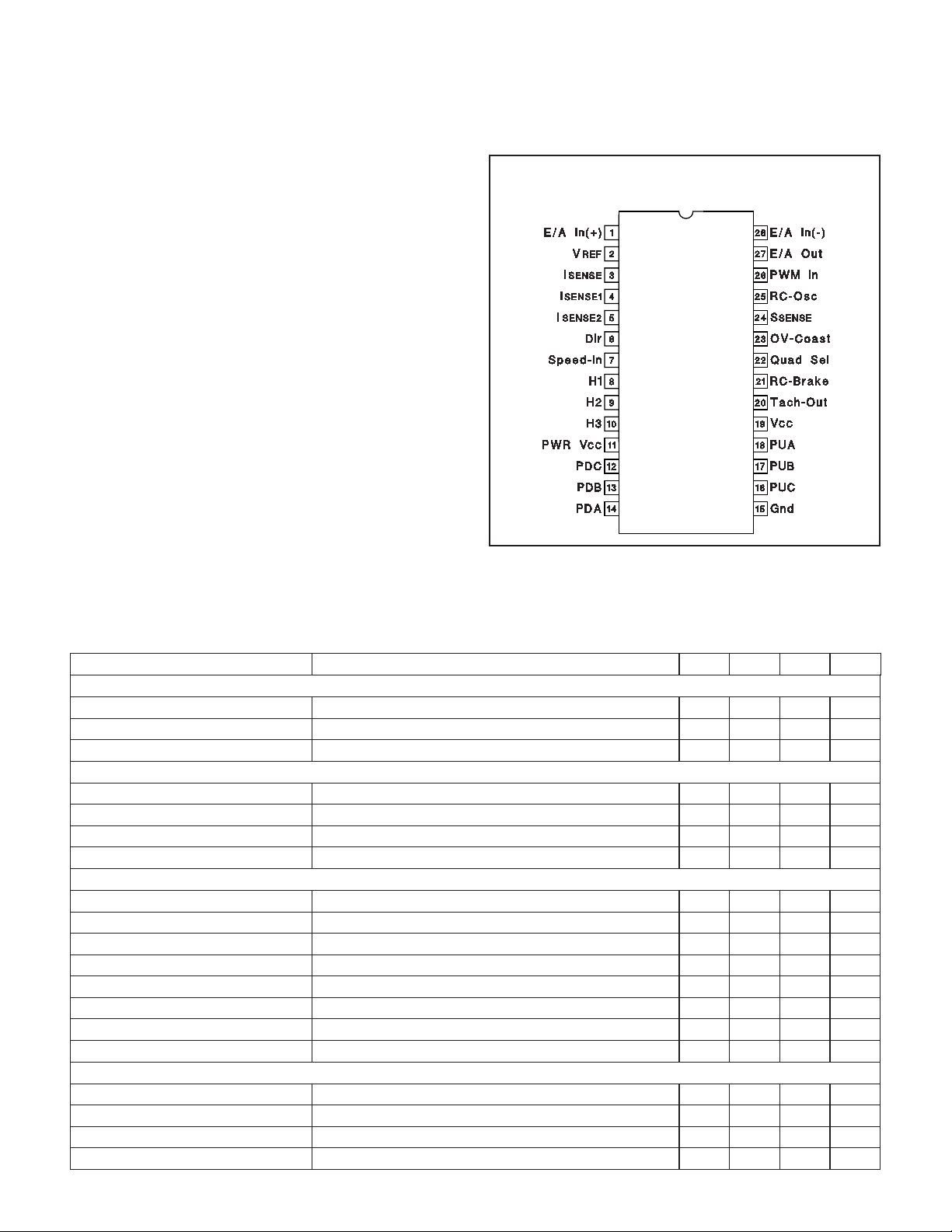
CONNECTION DIAGRAM
DIL-28 (TOP VIEW)
J or N PACKAGE
Note 1: Currents are positive into and negative out of the spec
-
ified terminal.
Note 2: Consult Unitrode Integrated Circuits databook for infor
mation regarding thermal specifications and limitations
of packages.
Note 3: This pinout applies to the SOIC (DW), PLCC (Q), and
LCC (L) packages (ie. pin 22 has the same function on all
packages.)
ELECTRICAL CHARACTERISTICS: Unless otherwise stated, these specifications apply for: TA= 25°C; Pwr VCC= VCC= 12V;
R
OSC
20k to V
=
REF
; C
OSC
= 2nF; R
TACH
= 33k; C
= 10nF; and all outputs unloaded. TA= T
TACH
.
J
PARAMETER TEST CONDITIONS MIN TYP MAX UNITS
Overall
Supply current Over Operating Range 14.5 30.0 mA
Turn-On Threshold Over Operating Range 8.65 8.95 9.45 V
V
CC
V
Turn-Off Threshold Over Operating Range 7.75 8.05 8.55 V
CC
Overvoltage/Coast
OV-Coast Inhibit Threshold Over Operating Range 1.65 1.75 1.85 V
OV-Coast Restart Threshold 1.55 1.65 1.75 V
OV-Coast Hysteresis 0.05 0.10 0.15 V
OV-Coast Input Current –10 –1 0 µA
Logic Inputs
H1, H2, H3 Low Threshold Over Operating Range 0.8 1.0 1.2 V
H1, H2, H3 High Threshold Over Operating Range 1.6 1.9 2.0 V
H1, H2, H3 Input Current Over Operating Range, to 0V -400 -250 –120 µA
Quad Sel, Dir Thresholds Over Operating Range 0.8 1.4 2.0 V
Quad Sel Hysteresis 70 mV
Dir Hysteresis 0.6 V
Quad Sel Input Current –30 50 150 µA
Dir Input Current –30 –1 30 µA
PWM Amp/Comparator
E/A In(+), E/A In(–) Input Current To 2.5V –5.0 –0.1 5.0 µA
PWM In Input Current To 2.5V 0 3 30 µA
Error Amp Input Offset 0V < V
COMMON-MODE
< 3V –10 10 mV
Error Amp Voltage Gain 70 90 dB
2

UC1625
UC2625
UC3625
ELECTRICAL CHARACTERISTICS: Unless otherwise stated, these specifications apply for: TA= 25°C; Pwr VCC= VCC= 12V;
R
20k to V
=
OSC
PWM Amp/Comparator (cont.)
E/A Out Range 0.25 3.50 V
S
S
S
Pull-up Current To 0V –16 –10 –5 µA
START
Discharge Current To 2.5V 0.1 0.4 3.0 mA
START
START Restart Threshold
Current Amp
Gain I
; C
REF
OSC
= 2nF; R
TACH
= 33k; C
= 10nF; and all outputs unloaded. TA= T
TACH
.
J
PARAMETER TEST CONDITIONS MIN TYP MAX UNITS
0.1 0.2 0.3 V
SENSE1
= .3V, I
SENSE2
= .5V to .7V 1.75 1.95 2.15 V/V
Level Shift I
Peak Current Threshold I
Over Current Threshold I
I
I
Range I
SENSE1
SENSE1
, I
SENSE2
, I
SENSE2
SENSE1
Input Current To 0V –850 –320 0 µA
Offset Current To 0V
, I
SENSE2
SENSE1
SENSE1
SENSE1
= .3V, I
SENSE2
= 0V, Force I
= 0V, Force I
= .3V 2.4 2.5 2.65 V
SENSE2
SENSE2
0.14 0.20 0.26 V
0.26 0.30 0.36 V
±
±
2
12 µA
–1 2 V
Tachometer/Brake
Tach-Out High Level Over Operating Range, 10k to 2.5V 4.7 5 5.3 V
Tach-Out Low Level Over Operating Range, 10k to 2.5V 0.2 V
On Time 170 220 280 µs
On Time Change With Temp Over Operating Range 0.1 %
RC-Brake Input Current To 0V –4.0 –1.9 mA
Threshold to Brake, RC-Brake Over Operating Range 0.8 1.0 1.2 V
Brake Hysteresis, RC-Brake 0.09 V
Speed-In Threshold Over Operating Range 220 257 290 mV
Speed-In Input Current –30 –5 30 µA
Low-Side Drivers
Voh, –1mA, Down From V
CC
V Voh, –50mA, Down From V
Over Operating Range 1.60 2.1
Over Operating Range 1.75 2.2 V
CC
Vol, 1mA Over Operating Range 0.05 0.4 V
Vol, 50mA Over Operating Range 0.36 0.8 V
Rise/Fall Time 10% to 90% Slew Time, into 1nF 50 ns
High-Side Drivers
Vol, 1mA Over Operating Range 0.1 0.4 V
Vol, 50mA Over Operating Range 1.0 1.8 V
Leakage Current Output Voltage = 50V 25 µA
Fall Time 10% to 90% Slew Time, 50mA Load 50 ns
Oscillator
Frequency 40 50 60 kHz
Frequency Over Operating Range 35 65 kHz
Reference
Output Voltage 4.9 5.0 5.1 V
Output Voltage Over Operating Range 4.7 5.0 5.3 V
Load Regulation 0mA to –20mA Load –40 –5 mV
Line Regulation 10V to 18V V
CC
–10 –1 10 mV
Short Circuit Current Over Operating Range 50 100 150 mA
3

UC1625
UC2625
UC3625
ELECTRICAL CHARACTERISTICS: Unless otherwise stated, these specifications apply for: TA= 25°C; Pwr VCC= VCC= 12V;
R
OSC
=
20k to V
REF
; C
OSC
= 2nF; R
TACH
= 33k; C
= 10nF; and all outputs unloaded. TA= T
TACH
.
J
PARAMETER TEST CONDITIONS MIN TYP MAX UNITS
Miscellaneous
Output Turn-On Delay 1 µs
Output Turn-Off Delay 1 µs
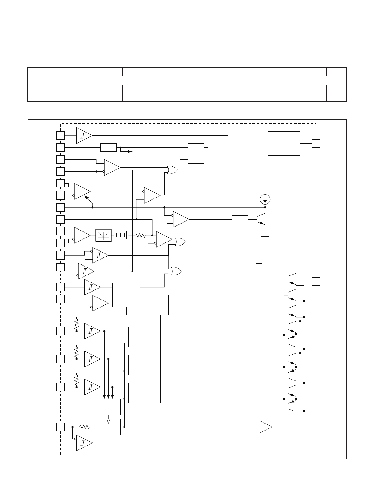
BLOCK DIAGRAM
Quad Sel
RC-Osc
PWM In
E/A Out
E/A In(+)
E/A In (–)
22
25
26
27
1
28
24SSTART
3ISENSE
4ISENSE1
5ISENSE2
19VCC
23OV-Coast
6Dir
7Speed-In
8H1
1.75V
9V
0.25V
+5V
+5V
ABS VALUE
2X
PWM CLOCK
OSC
DIRECTION
PWM CLOCK
2.9V
2.5V 250Ω
3.1V
LATCH
QD
L
SQ
R
0.2V
DIR COAST CHOP QUAD
H1
QR
S
PWM
CLOCK
REFERENCE
Q1
CROSS
CONDUCTION
PROTECTION
LATCHES
10µA
5V
2
VREF
18 PUA
17 PUB
16 PUC
11 Pwr Vcc
14 PDA
9H2
+5V
9H3
EDGE
DETECT
21RC-Brake
2k
1V
ONE
SHOT
QD
L
QD
L
H2
H3
DECODER
BRAKE
+5V
13 PDB
12 PDC
15 GND
20 Tach-Out
UDG-99044
4
 Loading...