

The UC1637 i s a p ul se width modulator circuit intended to be us ed for a variety of
PWM motor drive and amplifier applications requiring either uni-directional or bidirectional drive circuits. When used to replace conventional drivers, this circuit
can increase efficiency and reduce component costs for many applications. All
necessary circuitr y is included to generate an analog error signal and modulate
two bi-direc tional pulse train outpu ts in propor tion to the error signal magnitude
and polarity.
This monolithic device contains a sawtooth oscillator, error amplifier, and two
PWM compar ators with ±100mA output stages as standard features. Protection
circuitry includes under-voltage lockout, pulse-by-pulse current limiting, and a
shutdown port with a 2.5V temperature compensated threshold.
The UC1637 is characterized for operation over the full military temperature range
of -55°C to +125°C, while the UC2637 and UC3637 are characterized for -25°C to
+85°C and 0°C to +70°C, respectively.
Switched Mode Controller for DC Motor Drive
UC1637
UC2637
UC3637
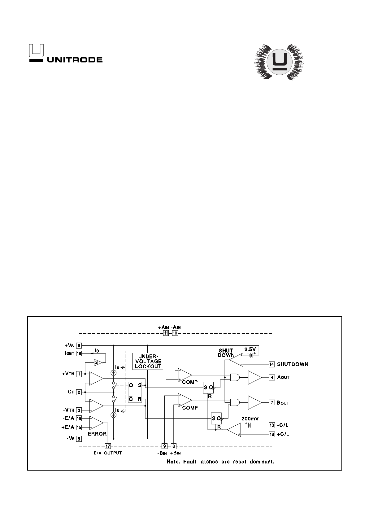
BLOCK DIAGRAM
• Single or Dual Supply
Operation
•
±
2.5V to ±20V Input Supply
Range
•
±
5% Initial Oscillator
Accuracy; ± 10% Over
Temperature
• Pulse-by-Pulse Current
Limiting
• Under-Voltage Lockout
• Shutdown Input with
Temperature Compensated
2.5V Threshold
• Uncommitted PWM
Comparators for Design
Flexibility
• Dual 100mA, Source/Sink
Output Drivers
Supply Voltage (±Vs) . . . . . . . . . . . . . . . . . . . . . . . . . . . . . . . . . . . . . . . . . . . . . . . . . . . ±20V
Output Current, Source/Sink (Pins 4, 7) . . . . . . . . . . . . . . . . . . . . . . . . . . . . . . . . . . . 500mA
Analog Inputs (Pins 1, 2, 3, 8, 9, 10, 11 12, 13, 14, 15, 16) . . . . . . . . . . . . . . . . . . . . . . . ±Vs
Error Amplifier Output Current (Pin 17) . . . . . . . . . . . . . . . . . . . . . . . . . . . . . . . . . . . ±20mA
Oscillator Charging Current (Pin 18). . . . . . . . . . . . . . . . . . . . . . . . . . . . . . . . . . . . . . . -2mA
Power Dissipation at TA = 25°C (Note 2) . . . . . . . . . . . . . . . . . . . . . . . . . . . . . . . . 1000mW
Power Dissipation at TC = 25°C (Note 2) . . . . . . . . . . . . . . . . . . . . . . . . . . . . . . . . 2000mW
Storage Temperature Range . . . . . . . . . . . . . . . . . . . . . . . . . . . . . . . . . . . -65°C to +150°C
Lead Temperature (Soldering, 10 Seconds). . . . . . . . . . . . . . . . . . . . . . . . . . . . . . . . +300°C
Note 1: Currents are positive into, negative out of the specified terminal.
Note 2: Consult Packaging Section of Databook for thermal limitations and considerations
of package.
FEATURES
ABSOLUTE MAXIMUM RATINGS (Note 1)
DESCRIPTION
6/97
UC1637
UC2637
UC3637
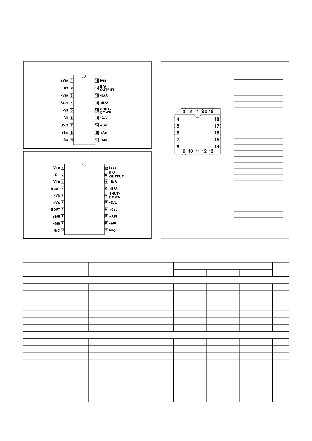
PACKAGE PIN
FUNCTION
FUNCTION PIN
+V
TH
1
C
T
2
-V
TH
3
A
OUT
4
-V
S
5
N/C 6
+V
S
7
B
OUT
8
+B
IN
9
-B
IN
10
-A
IN
11
+A
IN
12
+C/L 13
-C/L 14
SHUTDOWN 15
N/C 16
+E/A 17
-E/A 18
E/A
OUTPUT 19
I
SET
20
PLCC-20, LCC-20
(TOP VIEW)
Q, L Packages
ELECTRICAL CHARACTERISTICS:
PARAMETER TEST CONDITIONS UC1637/UC2637 UC3637 UNITS
MIN TYP MAX MIN TYP MAX
Oscillator
Initial Accuracy TJ = 25°C (Note 6) 9.4 10 10.6 9 10 11 kHz
Voltage Stability V
S
= ±5V to ±20V, V
PIN 1
= 3V,
V
PIN 3
= -3V
57 57%
Temperature Stability Over Operating Range (Note 3) 0.5 2 0.5 2 %
+V
TH
Input Bias Current V
PIN 2
= 6V -10 0.1 10 -10 0.1 10
µ
A
-V
TH
Input Bias Current V
PIN 2
= 0V -10 -0.5 -10 -0.5
µ
A
+V
TH,
-V
TH
Input Range +VS-2 -VS+2 +VS-2 -VS+2 V
Error Amplifier
Input Offset Voltage VCM = 0V 1.5 5 1.5 10 mV
Input Bias Current V
CM
= 0V 0.5 5 0.5 5
µ
A
Input Offset Current V
CM
= 0V 0.1 1 0.1 1
µ
A
Common Mode Range V
S
= ±2.5 to 20V -VS+2 +VS-VS+2 +V
S
V
Open Loop Voltage Gai n R
L
= 10k 75 100 80 100 dB
Slew Rate 15 15 V/
µ
S
Unity Gain Bandwidth 2 2 MHz
CMRR Over Common Mode Ra ng e 75 100 75 100 dB
PSRR VS = ±2.5 to ±20V 75 110 75 110 dB
CONNECTION DIAGRAM
Unless otherwise stated, these specifications apply for TA = -55°C to +125°C for the
UC1637; -25°C to +85°C for the UC2637; and 0°C to +70°C for the UC3637; +VS =
+15V, -VS = - 15V, +V
TH
= 5V, -V
TH
= -5V, RT = 16.7kΩ, CT = 1500pF, TA=T
J.
DIL-18 (TOP VIEW)
J or N Package
SOIC-20 (TOP VIEW)
DW Package
2

ELECTRICAL CHARACTERISTICS:
PARAMETERS TEST CONDITIONS UC1637/UC2637 UC3637 UNITS
MIN TYP MAX MIN TYP MAX
Error Amplifier (Continued)
Output Sink Current V
PIN 17
= 0V -50 -20 -50 -20 mA
Output Source Current V
PIN 17
= 0V 5 11 5 11 mA
High Level Output Voltage 13 13.6 13 13.6 V
Low Level Output V oltage -14.8 -13 -14.8 -13 V
PWM Comparators
Input Offset Voltage V
CM
= 0V 20 20 mV
Input Bias Current V
CM
= 0V 2 10 2 10
µ
A
Input Hysteresis V
CM
= 0V 10 10 mV
Common Mode range V
S
= ±5V to ±20V -VS+1 +VS-2 -VS+1 +VS-2 V
Current Limit
Input Offset Voltage V
CM
= 0V, TJ = 25°C 190 200 210 180 200 220 mV
Input Offset Voltage T.C. -0.2 -0.2 mV/°C
Input Bias Current -10 -1.5 -10 -1.5
µ
A
Common Mode Range V
S
= ±2.5V to ±20V -V
S
+VS-3 -V
S
+VS-3 V
Shutdown
Shutdown Threshold (Note 4) -2.3 -2.5 -2.7 -2.3 -2.5 -2.7 V
Hysteresis 40 40 mV
Input Bias Current V
PIN 14
= +VS to -V
S
-10 -0.5 -10 -0.5
µ
A
Under-Voltage Lockout
Start Threshold (Note 5) 4.15 5.0 4.15 5.0 V
Hysteresis 0.25 0.25 mV
Total Standby Current
Supply Current 8.5 15 8.5 15 mA
Output Section
Output Low Level I
SINK
= 20mA -14.9 -13 -14.9 -13 V
I
SINK
= 100mA -14.5 -13 -14.5 -13
Output High Level I
SOURCE
= 20mA 13 13.5 13 13.5 V
I
SOURCE
= 100mA 12 13.5 12 13.5
Rise Time (Note 3) C
L
= Inf, TJ = 25°C 100 600 100 600 ns
Fall Time (Note 3) C
L
= Inf, TJ = 25°C 100 300 100 300 ns
Note 3: These parameters, although guaranteed over the recommended operating conditions, are not 100% tested in production.
Note 4: Parameter measured with respect to +VS (Pin 6).
Note 5: Parameter measure d at +V
S
(Pin 6) with respect to -VS (Pin 5).
Note 6: R
T
and CT referenced to Ground.
UC1637
UC2637
UC3637
FUNCTIONAL DESCRIPTION
Following is a descr iption of each of the func tional blocks
shown in the Block Diagram.
Oscillator
The oscillator consists of two comparators, a charging
and discharg ing current source, a current source set ter minal, l
SET
and a flip- flop. The upper and lower threshold
of the oscilla tor waveform is set externally by applying a
voltage at pins +V
TH
and -VTH respectively. The +VTH ter-
minal voltage is buffered internally and also applied to the
l
SET
terminal to develop the capacitor charging current
through R
T
. If RT is referenced to -VS as shown in Figure
1, both the threshold voltage and charging current will
vary proportionally to the supply differential, and the oscillator frequency will remain constant. The triangle waveform oscillators frequency and voltage amplitude is
determ ined by the external components using the formulas
given in Figure 1.
Unless otherwise stated, these specifications apply for TA = -55°C to +125°C for the
UC1637; -25°C to +85°C for the UC2637; and 0°C to +70°C for the UC3637: VS =
+15V, -VS = - 15V, +V
TH
= 5V, -VTH = -5V, RT = 16.7kΩ, CT = 1500pF, TA=T
J.
3

UC1637
UC2637
UC3637
MODULATION SCHEMES
Case A Zero Deadtime
(Equal voltage on Pin 9 and Pin 11)
In this con figu rati on, m axi mum ho ldin g t orq ue or stiffnes s
and position accuracy is achieved. However, the power input into the motor is increased. Figure 3A shows this configuration.
Case B Small Deadtime
(Voltage on Pin 9 > Pin 11)
A small diffe renti al v olt age be tween Pin 9 and 11 pro vi de s
the necessary time delay to reduce the chances of momentary short circuit in the output stage during transitio ns, especially where power-amplifiers are used. Refer to
Figure 3B.
Case C Increased Deadtime and Deadband Mode
(Voltage on Pin 9 > Pin 11)
With the reduction of stiffness and position accuracy, the
power input into the motor around the null point of the
servo loop c an be reduce d or eliminat ed by widening the
window of the comparator circuit to a degree of acceptance. Where position accuracy and mechanical stiffness
is unimpor tant, de adband operat ion can be used. This is
shown in Figure 3C.
PWM Comparators
Two comparators are provided to perform pulse width
modulation for ea ch of the output drivers. Inputs are uncommitted to a llow m axi mum f lexibili ty. Th e pu lse width of
the outputs A and B is a function of the sign and amplitude of the er ror signa l. A negative signal at Pin 10 and 8
will lengthen the high state of output A and shorten the
high state of output B. Likewise, a positive error signal reverses the procedure. Typically, the oscillator waveform is
compared aga inst the summation of the error signal and
the level set on Pin 9 and 11.
Figure 1.
Oscillator Setup
Figure 2.
Comparator Bia sing
Output Drivers
Each output driver is cap ab le of both sour cing and si nki ng
100mA steady state and up to 500mA on a pulsed basis
for rapid switching of either POWERFET or bipolar transistors. Output levels are typically -V
S
+ 0.2V @50mA low
level and +V
S
- 2.0V @50mA high level.
Error Amplifier
The error amplifier consists of a high slew rate (15V/µs)
op-amp with a typical 1MHz bandwidth and low output impedance. Depending on the ±V
S
supply voltage, the common mode input range and the voltage output swing is
within 2V of the V
S
supply.
Under-V oltage Lockout
An under-voltage lockout circuit holds the outputs in the
low state un til a minimum o f 4V is reached. At this point,
all inter na l c irc u itry is functional and the output drivers are
enabled. If external circuitry requir es a high er starting v oltage, an over-riding voltage can be programmed through
the shutdown terminal as shown in Figure 4.
4

UC1637
UC2637
UC3637
Figure 3.
Modulation Schemes Showing (A) Zero Dea dt ime (B) Deadti me and (C) Deadban d Con figu ra ti ons
Shutdown Comparator
The shutdown terminal may be used for implementing
various shutdown and prot ection sc hemes. By pulling the
termin al mo re t han 2.5V below V
IN
, the output dr ivers w ill
be enabled. This can be realized using an open collector
gate or NPN transistor biased to either ground or the
negative supply. Since the threshold is temperature stabilized, the comparator can be used as an accurate low
voltage lockout (Figure 4) and/or delayed start as in Figure 5. In the shutdown m ode the outputs are held in the
low state.
Current Limit
A latched current limit amplifier with an internal 200mV
offset is p rovided to allow pulse-by-pulse current limiting.
Differential inputs will accept common mode signals from
-V
S
to within 3V of the +VS supply while providing excel-
lent
noise rejection. Figure 6 shows a typical current
sense circuit.
Figure 4.
External Under-Voltage Lockout
Figure 5.
Delayed Start-Up
Figure 6.
Current Limit Sensing
5

UC1637
UC2637
UC3637
Figure 7.
Bi-Directional Motor Drive with Speed Control Power-Amplifier
Figure 8.
Single Supply Position Servo Motor Drive
UNITRODE CORPORATION
7 CONTINENTAL BLVD. • MERRIMACK, NH 03054
TEL. (603) 424-2410 • FAX (603) 424-3460
6

IMPORTANT NOTICE
T exas Instruments and its subsidiaries (TI) reserve the right to make changes to their products or to discontinue
any product or service without notice, and advise customers to obtain the latest version of relevant information
to verify, before placing orders, that information being relied on is current and complete. All products are sold
subject to the terms and conditions of sale supplied at the time of order acknowledgement, including those
pertaining to warranty, patent infringement, and limitation of liability.
TI warrants performance of its semiconductor products to the specifications applicable at the time of sale in
accordance with TI’s standard warranty. Testing and other quality control techniques are utilized to the extent
TI deems necessary to support this warranty. Specific testing of all parameters of each device is not necessarily
performed, except those mandated by government requirements.
CERT AIN APPLICATIONS USING SEMICONDUCTOR PRODUCTS MAY INVOLVE POTENTIAL RISKS OF
DEATH, PERSONAL INJURY, OR SEVERE PROPERTY OR ENVIRONMENTAL DAMAGE (“CRITICAL
APPLICATIONS”). TI SEMICONDUCTOR PRODUCTS ARE NOT DESIGNED, AUTHORIZED, OR
WARRANTED TO BE SUITABLE FOR USE IN LIFE-SUPPORT DEVICES OR SYSTEMS OR OTHER
CRITICAL APPLICATIONS. INCLUSION OF TI PRODUCTS IN SUCH APPLICA TIONS IS UNDERSTOOD T O
BE FULLY AT THE CUSTOMER’S RISK.
In order to minimize risks associated with the customer’s applications, adequate design and operating
safeguards must be provided by the customer to minimize inherent or procedural hazards.
TI assumes no liability for applications assistance or customer product design. TI does not warrant or represent
that any license, either express or implied, is granted under any patent right, copyright, mask work right, or other
intellectual property right of TI covering or relating to any combination, machine, or process in which such
semiconductor products or services might be or are used. TI’s publication of information regarding any third
party’s products or services does not constitute TI’s approval, warranty or endorsement thereof.
Copyright 1999, Texas Instruments Incorporated
 Loading...