

Page 1
查询BGA供应商
Design Summary for
56GQL (48- and 56-pin functions)
MicroStar Junior
PCB Design Guidelines
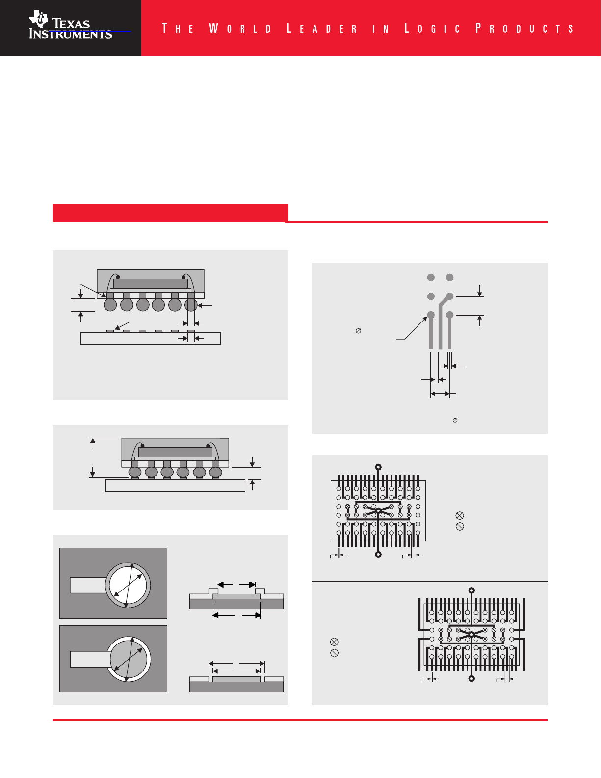
Package Via to Board Land Area Configuration
Package
ball via
0.2±0.05mm
(Not to scale)
Ratio A/B should equal 1.0 for optimum reliability
Overall Height
< 1.0 mm
MicroStar Junior Package
Land on PCB
PCB
A = Via diameter on package = 0.33 mm (for 0.65-mm pitch)
B = Land diameter on PCB
Solder Ball Collapse
PCB
(Not to scale)
VFBGA Recommended Land Pad Design
TM
BGA
Near-Sn/Pb
eutectic solder
with liquidus
temperature of
178°C to 210°C
A
B
0.2 mm
typical
Trace Width/Spacing Dimensions (mm [in.])
Non-Solder Mask Defined Pad
0.65 [.0256]
0.30 [.0118]
Solder Pad
0.117 [.0046] Trace
0.117 [.0046] min. space
0.65 [.0256]
Trace width/spacing for non-solder mask defined = 0.1167 [.0046]
Trace width/spacing for solder mask defined with 0.33 solder pad = 0.0733 [.0029]
Recommended Board Routing
V
CC
Recommended Routing
for VFBGA-48
GND
V
CC
Solder Mask Defined Pad
A
B
B
A
A = 0.43 mm
B = 0.33 mm
Non Solder M ask Defined Pad
A = 0.30 mm
B = 0.45 mm
B
A
B
A
0.117 MAX
[.0042]
Recommended Routing
for VFBGA-56
GND
V
CC
Note: Typical for most devices.
Refer to data sheet for
specific applications.
GND
0.320 MAX
[.0126]
Note: Typical for most devices.
Refer to data sheet for
specific applications.
0.117 MAX
[.0042]
GND
V
CC
0.320 MAX
[.0126]
Page 2
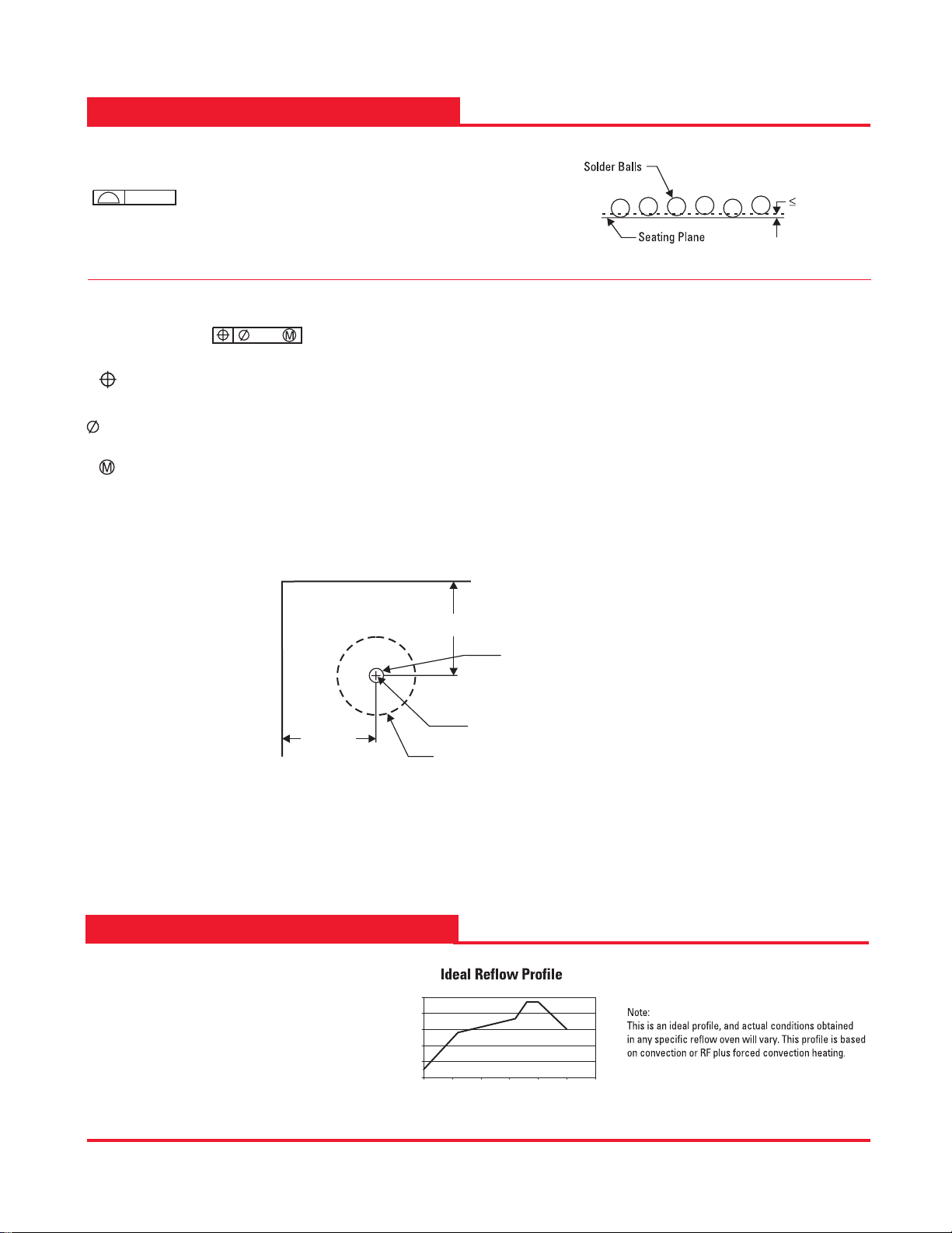
Geometric Dimensional Tolerances
Coplanarity
This geometric dimensioning and tolerancing (GD & T) term
means that this package meets a coplanarity of 0.08 mm
0,08 mm
as shown below. Coplanarity is defined as a unilateral tolerance zone
measured upward from the seating plane. (Reference ASME Y14.5-
1994).
Position Tolerance
0.08 mm
This GD & T term is described below:
0,05
This is the symbol for true position.
True position is defined as the theoretically exact centerline location of the solder ball(s).
This symbol/number represents how much the centerline of the solder ball(s) is allowed to vary from it's true position.
0,05
This symbol/letter is defined as the maximum material condition of the solder ball(s) which is 0.45 mm DIA.
The graphic representation is shown below for the top, left solder ball of this package.
Package End
*0.575 mm
Pattern locating boundary for the
centerline of the solder ball.
Package Side
* These two dimensions are calculated
based on a package with nominal
body width and length dimensions.
*0.625 mm
Pattern locating boundary containing the collective dimensions of the maximum size of
the solder ball (0.45 mm) and the maximum variance of the centerline of the solder
ball (0.05 mm) for a total boundary of 0.50 mm DIA.
I.E., the solder ball, regardless of size, must fall within this boundary. (Defined as
virtual condition per ASME standard Y14.5 - 1994).
Please note that a smaller diameter solder ball will have more tolerance in this
boundary than the maximum diameter solder ball.
(0.05 mm DIA.)
True position of the solder ball.
IR Reflow Profile
Ideal (1st and 2nd) Reflow Profile
Room Temp to 140°C: 60 - 90 sec.
140°C to 160°C: 90 - 120 sec.
Time above 200°C: 30 - 60 sec.
Peak Temp: 235°C ±5°C
Time within 5°C Peak Temp: 10-20 sec.
Ramp down rate: 1 - 3°C/sec. max.
250
200
150
100
50
Temperature (°C)
0
0 50 100 150 200 250 300
Time (seconds)
Page 3

Stencil Vitals
0.33 mm
0
.3
3
m
m
Packaging Tape and Reel
icrons
icrons
125 to 150 m
125 to 150 m
Solder Paste
TI recommends the use of paste when mounting MicroStar
Junior BGAs. The use of paste offers the following
advantages:
It acts as a flux to aid wetting of the solder ball to the PCB
land.
The adhesive properties of the paste will hold the
component in place during reflow.
Paste contributes to the final volume of solder in the joint,
and thus allows this volume to be varied to give an
optimum joint.
Paste selection is normally driven by overall system
assembly requirements. In general, the "no clean"
compositions are preferred due to the difficulty in cleaning
under the mounted components.
45
°
K
Quantity per reel = 1,000
Dimensions in millimeters
T
0.30 ± 0.05
0
B
6.3
0
A
0
B
0
K
0
F 7.50 ± 0.1
P
1
W 16.00 ± 0.3
(Not to scale)
D
1.55 ± 0.05
D
1
1.6 ± 0.1
R
0.3 Typical
4.80 ± 0.1
7.30 ± 0.1
1.50 ± 0.1
8.00 ± 0.1
P
2
0
Y
Y
2.0 ± 0.1
P
1
0.2
1.21.2
P
0
4.0 ± 0.1
3.8
A
0
Pin 1 Quadrant
F
Balls face down in pocket
Dimensions in millimeters
E
1.75 ± 0.1
W
Feed Direction
Reel Width
16.0
Reel Diameter
330
Cover Tape Width
13.5
Page 4

Package Outline
48/56GQL (4.5 x 7.0 mm, 0.65 mm pitch)
Pinout
4,60
4,40
3X Via Hole
Without
Ball
7,10
6,90
DEVICE
YMLLLLS
0,45
0,35
M
0,05
1,00 MAX
0,25
0,15
Missing Vi a
Hole Indicates
Pin A1
Quadrant
Seating Plane
0,08
0,65
K
J
H
G
F
E
D
C
B
A
123 645
Electrical Characteristics
R(ohms) L(nH) C(pF)
Min. 0.048 1.470 0.182
Mean 0.066 2.257 0.264
Max. 0.116 3.965 0.430
Thermal Characteristics
6.00
5.50
5.00
4.50
4.00
3.50
3.00
Power Dissipation (W)
2.50
2.00
1.50
20 30 40 50 60 70 80 90
4.50
4.00
3.50
3.00
2.50
Power Dissipation (W)
2.00
1.50
20 25 30 35 40 45 50 55 60 65 70 75 80 85 90 95
Eight Thermal Vias, High K
Ambient Temperature (ºC)
Without Thermal Vias, High K
Ambient Temperature (ºC)
Daisy Chain Net List
56GQL TOP VIEW
A1-B3 J4-K6
A2-A3 K4-K5
6
5
4
3
2
1
A
BCDEFGHJ K
A4-A5 K2-K3
A6-B4 J3-K1
B5-B6 J1-J2
C6-D5 G2-H1
C4-C5 H2-H3
D4-D6 G1-G3
E5-E6 F1-F2
F5-F6 E1-E2
G4-G6 D1-D3
H4-H5 C2-C3
G5-H6 C1-D1
J5-J6 B1-B2
3,25 TYP
0,325
0 lfm @ Tj=150ºC
150 lfm @ Tj=150ºC
250 lfm @ Tj=150ºC
500 lfm @ Tj=150ºC
0 lfm @ Tj=150ºC
150 lfm @ Tj=150ºC
250 lfm @ Tj=150ºC
500 lfm @ Tj=150ºC
0,325
0,65
5,85 TYP
Pinout for 48-pin functions
6 A48 A46 A43 A40 A37 A36 A33 A30 A27 A25
5 NC A47 A44 A41 A38 A35 A32 A29 A26 NC
4 NC *A45 A42 *A39 *A34 A31 *A28 NC
3 NC *A4 A7 *A10 *A15 A18 *A21 NC
2 NC A2 A5 A8 A11 A14 A17 A20 A23 NC
1 A1 A3 A6 A9 A12 A13 A16 A19 A22 A24
ABCDEFGHJK
Contr ol *GND V
Note: This is a topside view
CC
Pinout for 56-pin functions
6 A54 A51 A48 A45 A43 A42 A40 A37 A34 A31
5 A55 A52 A49 A47 A44 A41 A38 A36 A33 A30
4 A56 A53 A50 *A46 *A39 A35 *A32 A29
3 A1 A4 A7 *A11 *A18 A22 *A25 A28
2 A2 A5 A8 A10 A13 A16 A19 A21 A24 A27
1 A3 A6 A9 A12 A14 A15 A17 A20 A23 A26
ABCDEFGHJK
Contr ol *GND V
Note: This is a topside view
Package Reliability Data
Test Chip: ALVCH16501, 'B' Die Revision, 85 x 107 mils
Preconditioning: JEDEC Level 2 (85°C/60% 168 hr + 3IRR 220°C)
Simultaneous Switching Life Test
(SSLT), 150°C, 300 Hours
Highly Accelerated Life Test (HAST),
130°C, 85% RH, 100 Hours
Temperature Cycle Test, -65°C to
150°C, 1000 Hours
Autoclave, 121°C, 96 Hours 77 / 0 77 / 0
Solderability, 8 Hours 8 / 0 8 / 0
Flammability (UL) 5 / 0 5 / 0
Flammability (IEC) 5 / 0 5 / 0
Thermal Shock 26 / 0 26 / 0
X-Ray, Top View Only 5 / 0 5 / 0
Physical Dimensions 15 / 0 15 / 0
Manufacturability pass pass
Sample Size /
Board Level Reliability Data
56 GQL Package
Sample Size = 32
Temp Cycle Range -40°C to 125°C
No Underfill
Board Thickness (mm) 1.6 0.8 0.8, no Au
0 cycle 000
250 cycle 000
500 cycle 000
750 cycle 000
1000 cycle 2* 0 0
1250 cycle 15 1 0
1500 cycle 19 8 0
1750 cycle N/A 20 1
2000 cycle N/A N/A 0
* First failure at 951 cycles
t = 0.8 mm, with Au, 50% failure = 1733 cycles
CC
Required
ALVCH16501GQL
Actual Sample Size /
#Fails
39 / 0 39 / 0
39 / 0 39 / 0
77 / 0 77 / 0
# Fails
Page 5

Sockets
Yamaichi Socket Numbers:
VFBGA-56 PN# IC280-056-237
Questions and Answers
Board Design/Electrical Issues
Q. Where can the decoupling capacitors go for the VFBGA package?
A. The recommended capacitance value and number of capacitors for decoupling
is a 0.1 mF capacitor for each VCC on the VFBGA package. The decoupling
capacitors should be connected as close as possible to the GROUND and VCC
planes.
Q. Any EMI concerns for traces under the package and how can customers
design their board to minimize EMI?
A. EMI can be controlled by minimizing any complex current loops on the PCB
trace. Some helpful hints include:
Solid ground and power planes be used in the design. Partitioned ground
and power planes must be avoided. These ground and power partitions
may create complex current loops increasing radiation.
Avoid right angles or "T" crosses on the trace. Right angles can cause
impedance mismatch and increase trace capacitance causing signal
degradation.
Minimize power supply loops by keeping power and ground traces parallel
and adjancent to each other. Significant package EMI can be reduced by
using this method.
Use decoupling capacitors as described in the previous question.
Lead-Free
Q. Should I use underfill?
A. No, the package qualification results show that this is not necessary and is only
an added process expense.
Q. Can the boards be repaired?
A. Yes, there are rework and repair tools and profiles available (see references 4
and 7). We strongly recommend that removed packages be discarded.
Q. How do the board assembly yields of MicroStar Junior BGAs compare to
TSSOPs?
A. Many customers are initially concerned about assembly yields. However, once
they had MicroStar Junior BGAs in production, most of them report improved
process yields compared to TSSOPs. This is due to the elimination of bent and
misoriented leads, the wider terminal pitch than with 0.5-mm pitch TSSOPs,
and the ability of these packages to self align during reflow. The collapsing
solder balls also mean that the coplanarity is improved over leaded
components.
Q. What alignment accuracy is possible?
A. Alignment accuracy for the 0.65-mm pitch package is dependent upon board
level pad tolerance, placement accuracy, and solder ball position tolerance.
Nominal ball position tolerances are specified at ±50 microns. These packages
are self-aligning during solder reflow, so final alignment accuracy may be better
than placement accuracy.
Q. Are there specific recommendations for SMT processing?
A. Texas Instruments recommends alignment with the solder balls for the CSP
package, although it is possible to use the package outline for alignment. Most
customers have found they do not need to change their reflow profile.
Q. Can the solder joints be inspected after reflow?
A. Process yields of 5-ppm rejects are typically seen, so no final inline inspection
is required. Some customers are achieving satisfactory results during process
setup with lamographic X-ray techniques.
Package (Incoming Inspection)
Q. Is package repair possible? Are tools available?
A. Yes, some limited package repair is possible, and there are some semi-auto
M/C tools available. However, TI does not guarantee the reliability of repaired
packages.
Q. Do the solder balls come off during shipping?
A. No, this has never been observed. The balls are 100 percent inspected for
coplanarity, diameter and other physical properties prior to packing for
shipment. Because solder is used during the ball attachment process, uniformly
high ball attachment strengths are developed. Also, the ball attachment
strength is monitored frequently in the assembly process to prevent ball loss
from vibration and other shipping forces.
Q. Is TI developing a lead-free version of MicroStar Junior BGAs?
A. Yes, Texas Instruments is working toward eliminating lead in the solder balls to
comply with lead-free environmental policies. The lead-free solder is in final
evaluation. Only the solder will change, not the package structure or the
mechanical dimensions. The solder system under development is based on
Sn-Cu-Ag metallurgy. Check with your local TI Field Sales representative for
sample availability.
Assembly Process/Yield Considerations
Q. What size land diameter for these packages should I design on my
board?
A. Land size is the key to board-level reliability, and Texas Instruments strongly
recommends following the design rules included in this bulletin.
Q. Can customers mount MicroStar Junior BGA packages on the bottom
side of the PCB board?
A. Yes, they can and the ideal 2nd reflow profile is the same as the 1st (IR profile
is recommended in the bulletin). The root causes for solder ball off are:
Excess amount of solder paste during customers board assembly. TI
recommends minimizing the amount of solder paste on the bottom side by
using a stencil thickness of 0.15 mm with 0.33-mm aperture opening.
Moisture absorption also affects the ball off issue. The package was
qualified at Moisture Level 2, and has been released at Moisture Level 2A.
The first and second reflow must be completed within 4 weeks.
References
Recommended References:
1. MicroStar BGA Packaging Reference Guide - SSYZ015
2. 96 and 114 ball LFBGA Application Note - IDT, Philips Semiconductor and Texas
Instruments
3. Board Level Reliability Evaluations of 40, 32 and 30 Mil Pitch Ball Grid Array
Packages Over -40 to 125°C - Puligandla Viswanadham, Steve Dunford and
Ted Carper, Circuit Card Assemblies Center of Excellence Raytheon Systems
Co.
4. Comprehensive User's Guide for µBGA*Packages www.intel.com/design/flcomp/packdata/297846.htm
5. Solder Paste Printing Guidelines for BGA and CSP Assemblies - Donald C. Burr,
published in SMTJanuary 1999.
6. Maintaining BGA Reliability During Rework - Stuart Downes and Robert Farrell,
published in SMT January 1999.
7. BGA Rework Considerations - Jennie S. Hwang, published in SMT November
1998.
Page 6

TI Worldwide Technical Support
Internet
TI Semiconductor Home Page
www.ti.com/sc
MicroStar Junior BGA Home Page
www.ti.com/sc/msjunior
TI Distributors
www.ti.com/sc/docs/general/distrib.htm
Product Information Centers
Americas
Phone +1(972) 644-5580
Fax +1(214) 480-7800
Internet www.ti.com/sc/ampic
Europe, Middle East, and Africa
Phone
Belgium (English) +32 (0) 27 45 55 32
France +33 (0) 1 30 70 11 64
Germany +49 (0) 8161 80 33 11
Israel (English) 1800 949 0107
Italy 800 79 11 37
Netherlands (English) +31 (0) 546 87 95 45
Spain +34 902 35 40 28
Sweden (English) +46 (0) 8587 555 22
United Kingdom +44 (0) 1604 66 33 99
Fax +44 (0) 1604 66 33 34
Email epic@ti.com
Internet www.ti.com/sc/epic
Logic Overview Page
www.ti.com/sc/logic
Phone
International +886-2-23786800
Domestic Local Access Code TI Number
Australia 1-800-881-011 -800-800-1450
China 10810 -800-800-1450
Hong Kong 800-96-1111 -800-800-1450
India 000-117 -800-800-1450
Indonesia 001-801-10 -800-800-1450
Korea 080-551-2804 Malaysia 1-800-800-011 -800-800-1450
New Zealand 000-911 -800-800-1450
Philippines 105-11 -800-800-1450
Singapore 800-0111-111 -800-800-1450
Taiwan 080-006800 Thailand 0019-991-1111 -800-800-1450
Fax 886-2-2378-6808
Email tiasia@ti.com
Internet www.ti.com/sc/apic
Japan
Phone
International +81-3-3344-5311
Domestic 0120-81-0026
Fax
International +81-3-3344-5317
Domestic 0120-81-0036
Internet
International www.ti.com/sc/jpic
Domestic www.tij.co.jp/pic
Asia
MicroStar BGA and MicroStar Junior are trademarks of
Texas Instruments Incorporated
© Copyright 2000 Texas instruments Incorporated
Important Notice: The products and services of Texas
Instruments and its subsidiaries described herein are sold
subject to TIs standard terms and conditions of sale. Customers
are advised to obtain the most current and complete information
about TI products and services before placing orders. TI
assumes no liability for applications assistance, customers
applications or product designs, software performance, or
infringement of patents. The publication of information regarding
any other companys products or services does not constitute
TIs approval, warranty or endorsement thereof.
SCET004
 Loading...