

Page 1

The Embedded I/O Company
TPMC671
16 Digital Inputs (24V)
16 Digital Outputs (24V, 0.5A)
Version 1.0
User Manual
Issue 1.1
October 2004
TEWS TECHNOLOGIES GmbH
Am Bahnhof 7 25469 Halstenbek / Germany
Phone: +49-(0)4101-4058-0 Fax: +49-(0)4101-4058-19
e-mail: [email protected] www.tews.com
TEWS TECHNOLOGIES LLC
1 E. Liberty Street, Sixth Floor Reno, Nevada 89504 / USA
Phone: +1 (775) 686 6077 Fax: +1 (775) 686 6024
e-mail: [email protected] www.tews.com
Page 2

TPMC671-10
16 digital inputs, 16 digital high side switch
outputs, front panel I/O
TPMC671-11
16 digital inputs, 16 digital low side switch
outputs, front panel I/O
TPMC671-20
16 digital inputs, 16 digital high side switch
outputs, P14 I/O
TPMC671-21
16 digital inputs, 16 digital low side switch
outputs, P14 I/O
This document contains information, which is
proprietary to TEWS TECHNOLOGIES GmbH. Any
reproduction without written permission is forbidden.
TEWS TECHNOLOGIES GmbH has made any
effort to ensure that this manual is accurate and
complete. However TEWS TECHNOLOGIES GmbH
reserves the right to change the product described
in this document at any time without notice.
TEWS TECHNOLOGIES GmbH is not liable for any
damage arising out of the application or use of the
device described herein.
Style Conventions
Hexadecimal characters are specified with prefix 0x,
i.e. 0x029E (that means hexadecimal value 029E).
For signals on hardware products, an ‘Active Low’ is
represented by the signal name with # following, i.e.
IP_RESET#.
Access terms are described as:
W Write Only
R Read Only
R/W Read/Write
R/C Read/Clear
R/S Read/Set
2004 by TEWS TECHNOLOGIES GmbH
Issue Description Date
1.0 First Issue September 2004
1.1 Correction of PCI Header October 2004
TPMC671 User Manual Issue 1.1 Page 2 of 28
Page 3

Table of Contents
1 PRODUCT DESCRIPTION.........................................................................................5
2 TECHNICAL SPECIFICATION...................................................................................6
3 FUNCTIONAL DESCRIPTION ...................................................................................7
3.1 Digital Outputs ................................................................................................................................7
3.1.1 Optical Isolation....................................................................................................................7
3.1.2 Output Polarity......................................................................................................................7
3.1.3 Overload Protection..............................................................................................................7
3.1.4 Output Watchdog..................................................................................................................8
3.2 Digital Inputs ...................................................................................................................................8
3.2.1 Optical Isolation....................................................................................................................8
3.2.2 Debounce Function...............................................................................................................8
3.2.3 Interrupt Logic.......................................................................................................................8
4 LOCAL SPACE ADDRESSING..................................................................................9
4.1 PCI9030 Local Space Configuration .............................................................................................9
4.2 Local Register Space Address Map..............................................................................................9
4.2.1 Data Output Register..........................................................................................................10
4.2.2 Data Input Register.............................................................................................................11
4.2.3 Control / Status Register ....................................................................................................12
4.2.4 Rising Edge Interrupt Enable Register...............................................................................13
4.2.5 Falling Edge Interrupt Enable Register...............................................................................14
4.2.6 Rising Edge Interrupt Status Register................................................................................15
4.2.7 Falling Edge Interrupt Status Register................................................................................16
4.2.8 Debounce Time Register....................................................................................................17
5 PCI9030 TARGET CHIP...........................................................................................19
5.1 PCI Configuration Registers (PCR).............................................................................................19
5.1.1 PCI9030 Header.................................................................................................................19
5.1.2 PCI Base Address Initialization ..........................................................................................20
5.2 Local Configuration Register (LCR)............................................................................................21
5.3 Configuration EEPROM................................................................................................................22
5.4 Local Software Reset....................................................................................................................23
6 CONFIGURATION HINTS........................................................................................24
6.1 Software Reset (Controller and LRESET#).................................................................................24
6.2 Big / Little Endian..........................................................................................................................24
7 INSTALLATION........................................................................................................ 26
7.1 Input Wiring ...................................................................................................................................26
7.2 Output Wiring High Side Switch (-10 / -20).................................................................................26
7.3 Output Wiring Low Side Switch (-11 / -21)..................................................................................26
8 PIN ASSIGNMENT – I/O CONNECTOR ..................................................................27
8.1 Front Panel Connector .................................................................................................................27
8.2 Mezzanine Card Connector P14 ..................................................................................................28
TPMC671 User Manual Issue 1.1 Page 3 of 28
Page 4

Table of Figures
FIGURE 1-1 : BLOCK DIAGRAM......................................................................................................................5
FIGURE 2-1 : TECHNICAL SPECIFICATION...................................................................................................6
FIGURE 3-1 : ISOLATED DIGITAL OUTPUTS.................................................................................................7
FIGURE 4-1 : PCI9030 LOCAL SPACE CONFIGURATION............................................................................9
FIGURE 4-2 : FPGA REGISTER SPACE.........................................................................................................9
FIGURE 4-3 : DATA OUTPUT REGISTER.....................................................................................................10
FIGURE 4-4 : DATA INPUT REGISTER.........................................................................................................11
FIGURE 4-5 : CONTROL / STATUS REGISTER...........................................................................................12
FIGURE 4-6 : RISING EDGE INTERRUPT ENABLE REGISTER..................................................................13
FIGURE 4-7 : FALLING EDGE INTERRUPT ENABLE REGISTER...............................................................14
FIGURE 4-8 : RISING EDGE INTERRUPT STATUS REGISTER..................................................................15
FIGURE 4-9 : FALLING EDGE INTERRUPT STATUS REGISTER...............................................................16
FIGURE 4-10: DEBOUNCE TIME REGISTER................................................................................................17
FIGURE 4-11: FORMULAS TO DETERMINE PRELOAD VALUE..................................................................17
FIGURE 4-12: DEBOUNCE TIME / EXAMPLES.............................................................................................18
FIGURE 5-1 : PCI9030 HEADER....................................................................................................................19
FIGURE 5-2 : PCI9030 PLD BASE ADDRESS USAGE.................................................................................20
FIGURE 5-3 : PCI9030 LOCAL CONFIGURATION REGISTER....................................................................21
FIGURE 5-4 : CONFIGURATION EEPROM TPMC671-XX ...........................................................................22
FIGURE 6-1 : LOCAL BUS LITTLE/BIG ENDIAN...........................................................................................24
FIGURE 7-1 : INPUT WIRING.........................................................................................................................26
FIGURE 7-2 : OUTPUT WIRING HIGH SIDE SWITCH..................................................................................26
FIGURE 7-3 : OUTPUT WIRING LOW SIDE SWITCH ..................................................................................26
FIGURE 8-1 : PIN ASSIGNMENT I/O HD68 SCSI-3 TYPE CONNECTOR...................................................27
FIGURE 8-2 : MEZZANINE CARD CONNECTOR P14..................................................................................28
TPMC671 User Manual Issue 1.1 Page 4 of 28
Page 5
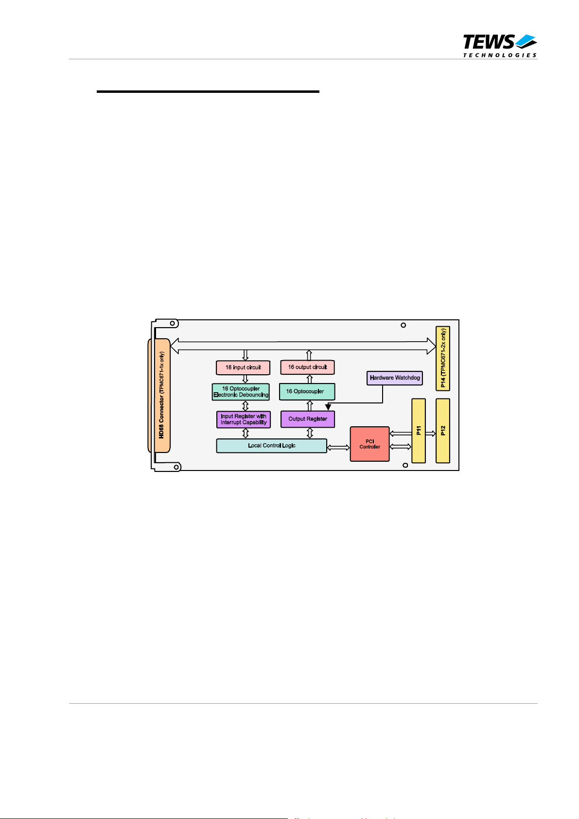
1 Product Description
The TPMC671 is a standard single-width 32 bit PMC with 16 digital inputs (24V) galvanically isolated
from the computer system by optocouplers. The inputs are also potential free to each other. A high
performance input circuit ensures a defined switching point and polarization protection against
confusing the pole.
All inputs have a common electronic debounce circuit with a freely programmable debounce time.
All inputs can generate an interrupt. The signal edge handling is programmable to interrupt on rising,
falling or both edges of the input signal.
The TPMC671 has 16 digital high side or low side switches (build option) with galvanic isolation from
the computer system by optocouplers. The outputs are isolated against each other in groups of four
outputs. All outputs are protected against short-circuit and thermal overload. The output drivers are
capable of driving 0.5A continuous per channel.
A hardware watchdog clears all outputs in case of trigger fail. The TPMC671-1x provides front panel
I/O, the TPMC671-2x provides P14 I/O.
Figure 1-1 : Block Diagram
TPMC671 User Manual Issue 1.1 Page 5 of 28
Page 6

2 Technical Specification
Mechanical Interface
Electrical Interface
On Board Devices
PCI Target Chip
I/O Interface
Number of Inputs
Input Isolation
Input Voltage
Input Current
Input Switching Level
Input Signal Debouncing
Input Interrupts
Outputs
Output Isolation
External Output Voltage
Output Current
Short Circuit Current
Output Voltage Drop
Output Protection
I/O Connector
Physical Data
PCI Mezzanine Card (PMC) Interface
Single Size
PCI Rev. 2.1 compliant
33 MHz / 32 bit PCI
3.3V and 5V PCI Signaling Voltage
PCI9030 (PLX Technology)
16 digital Inputs
Optocouplers for galvanic isolation, also isolated to each other
24V DC typical
4.2mA typical at 24V input voltage
12V typical, 7.5V minimum, 14V maximum
Electronic debouncing ( 7µs to 440 ms in steps of 7µs )
common for all input channels, can be disabled
16 input interrupts (Trigger on rising, falling or both edges)
TPMC671-10 / -20
TPMC671-11 / -21
Optocouplers for galvanic isolation, also isolated to each other in
groups of four outputs
24V DC typical, 6V DC minimum, 48V DC maximum
0.5A typical ( 0.3A for voltages over 32V )
0.8A typical
1.1V typical at 0.5A
Overload, short circuit, GND and Vs open wire protection, thermal
shutdown
TPMC671-10 / -11
TPMC671-20 / -21
16 digital high side switch Outputs
16 digital low side switch Outputs
HD68 connector SCSI-3 type connector
PMC P14 I/O (64 pin Mezzanine connector)
Power Requirements
Temperature Range
MTBF
Humidity
Weight
TPMC671 User Manual Issue 1.1 Page 6 of 28
85 mA typical @ +3.3V DC with all inputs and outputs inactive
200 mA typical @ +3.3V DC with all inputs and outputs active
Operating
Storage
252000 h
5 – 95 % non-condensing
72 g
Figure 2-1 : Technical Specification
-25 °C to +85 °C
-55°C to +125°C
Page 7

3 Functional Description
3.1 Digital Outputs
3.1.1 Optical Isolation
The TPMC671 has 16 high side switch (TPMC671-10/20) or 16 low side switch (TPMC671-11/21)
digital outputs. The standard signal level for these outputs is 24V DC. All outputs are isolated by
optocouplers from the computer system and are also isolated against each other in groups of four
outputs.
GROUP VS / standard 24V DC GROUND OUTPUT
O1 VS_O1 GND_O1 OUT 1
OUT 2
OUT 3
OUT 4
O2 VS_O GND_O2 OUT 5
OUT 6
OUT 7
OUT 8
O3 VS_O3 GND_O3 OUT 9
OUT 10
OUT 11
OUT 12
O4 VS_O4 GND_O4 OUT 13
OUT 14
OUT 15
OUT 16
Figure 3-1 : Isolated Digital Outputs
3.1.2 Output Polarity
Each output can be individually switched to the according power supply VS_Ox (high side switch) or
GND_Ox (low side switch).
3.1.3 Overload Protection
The output drivers used on the TPMC671 are smart drivers TDE1707. The maximum continuous
output current is 0.5A. The output circuits are protected against overload, short circuit and over
temperature. In case of such a failure the corresponding output is switched off until the error condition
is removed. Then the output returns automatically to normal operation and the state programmed in
the Data Output Register.
For details about the protection of the TDE1707 please refer to the data sheet which is part of the
TPMC671-ED Engineering Documentation.
TPMC671 User Manual Issue 1.1 Page 7 of 28
Page 8

3.1.4 Output Watchdog
Writing ‘1’ into bit 1 of the Global Control Register enables the hardware watchdog function. The
status of the watchdog is indicated at the bit 3 of Global Control Register.
Any software access (read or write) to the Data Output Register of the TPMC671 will retrigger the
watchdog. The maximum time between two accesses is set to 120ms, if the time expires without a
software access all outputs go into the ‘OFF’ state. At the same time the watchdog status will change
from ‘0’ to ‘1’ and lock the Data Output Register. This prevents a write access to the Data Output
Register.
Writing ‘1’ to the watchdog status (Bit 3 Control Register) clears this bit and also unlocks the Output
Register. After unlocking the Data Output Register, the outputs stays in the ‘OFF’ state till the next
write access to this Register.
The watchdog is disabled after power-on or reset.
3.2 Digital Inputs
3.2.1 Optical Isolation
The TPMC671 has 16 digital inputs. The standard signal level for these inputs is 24V DC. The
switching level of the inputs is between 7.5V and 14V. All inputs are isolated by optocouplers from the
computer system and are also isolated against each other.
3.2.2 Debounce Function
A programmable debounce function common for all inputs is implemented on the TPMC671. There is
only one debounce time adjustable for all 16 digital inputs.
If the debounce function is enabled, the input pin must be static for the programmed debounce time
before the rising or falling edge is recognized as valid. So only after a correct identification the Data
Input Register is updated and an interrupt is generated.
The debounce function is disabled after power-on and reset. The debounce time is set to value
‘0’ after power-on and reset.
3.2.3 Interrupt Logic
Interrupt generation can be individually programmed for each channel and input transition. To enable
the interrupt after a reset, the Global Interrupt Enable bit in the Control Register must be set to the
value ‘1’. Also the respective bit for rising or falling edge in the Rising Edge / Falling Edge Interrupt
Enable Registers must be set.
The Global Interrupt Enable and also all individually interrupt enable bits are disabled after
power-on and reset.
TPMC671 User Manual Issue 1.1 Page 8 of 28
Page 9
4 Local Space Addressing
4.1 PCI9030 Local Space Configuration
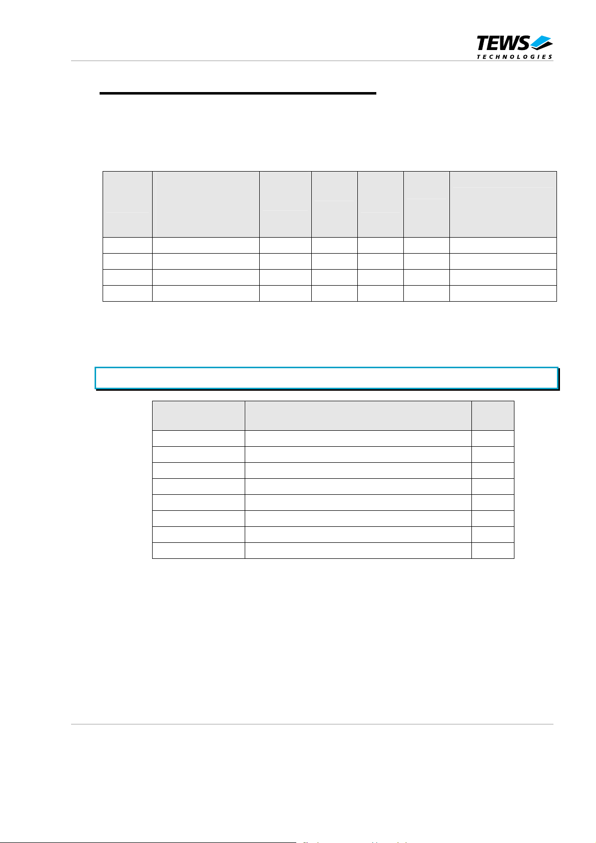
The local on board addressable regions are accessed from the PCI side by using the PCI9030 local
spaces.
PCI9030
Local
Space
0 2 (0x18) IO 16 16 BIG Local Register Space
1 3 (0x1C) - - - - Not Used
2 4 (0x20) - - - - Not Used
3 5 (0x24) - - - - Not Used
PCI9030
PCI Base Address
(Offset in PCI
Configuration
Space)
Figure 4-1 : PCI9030 Local Space Configuration
PCI
Space
Mapping
Size
(Byte)
Port
Width
(Bit)
Endian
Mode
Description
4.2 Local Register Space Address Map
PCI Base Address: PCI9030 PCI Base Address 2 (Offset 0x18 in PCI Configuration Space).
Offset to PCI
Base Address 2
0x00 Data Output Register 16
0x02 Data Input Register 16
0x04 Control / Status Register 16
0x06 Rising Edge Interrupt Enable Register 16
0x08 Falling Edge Interrupt Enable Register 16
0x0A Rising Edge Interrupt Status Register 16
0x0C Falling Edge Interrupt Status Register 16
0x0E Debounce Time Register 16
Register Name Size
(Bit)
Figure 4-2 : FPGA Register Space
TPMC671 User Manual Issue 1.1 Page 9 of 28
Page 10

4.2.1 Data Output Register
The Data Output Register is a word wide read/write register that is used to set or clear the different
outputs of the TPMC671.
Bit Symbol Description Access
15 OUTPUT16
14 OUTPUT15
13 OUTPUT14
12 OUTPUT13
11 OUTPUT12
10 OUTPUT11
9 OUTPUT10
8 OUTPUT9
7 OUTPUT8
6 OUTPUT7
5 OUTPUT6
4 OUTPUT5
3 OUTPUT4
2 OUTPUT3
1 OUTPUT2
0 OUTPUT1
To set an output line active, write ‘1’ to the corresponding
bit.
For the inactive state write ‘0’ to the corresponding bit.
0 : inactive
1 : active
Bit 0 represents output line 1 and bit 15 represents
output line 16.
After power-on or reset the Data Output Register is
cleared to ‘0’, all outputs are inactive.
R/W
Figure 4-3 : Data Output Register
Reset
Value
0x0000
TPMC671 User Manual Issue 1.1 Page 10 of 28
Page 11

4.2.2 Data Input Register
The Data Input Register is a word wide read only register that reflects the actual status of the inputs.
Bit Symbol Description Access
15 INPUT16
14 INPUT15
13 INPUT14
12 INPUT13
11 INPUT12
10 INPUT11
9 INPUT10
8 INPUT9
7 INPUT8
6 INPUT7
5 INPUT6
4 INPUT5
3 INPUT4
2 INPUT3
1 INPUT2
0 INPUT1
0 : Input line is logic low
1 : Input line is logic high
Bit 0 represents Input Line 1 and bit 15 represents the
Input Line 16.
R
Figure 4-4 : Data Input Register
Reset
Value
-
TPMC671 User Manual Issue 1.1 Page 11 of 28
Page 12

4.2.3 Control / Status Register
The Control / Status Register is a read/write register.
Bit Symbol Description Access
15 : 4 -
3 WD_STA
Not used and undefined during reads
Watchdog Status Flag
- -
R/W 0
1 = indicates that the watchdog had
recognized a failure and had disabled
all output channels. Also the Output
Register is locked.
0 = clears this bit and unlocks Output
Register
2 DB_ENA
Debounce Enable
R/W 0
1 = enables the debounce function for all
16 inputs
0 = disables debounce function
1 WD_ENA
Watchdog Enable
R/W 0
1 = enables watchdog for all 16 outputs
0 = disables watchdog function
0 INT_ENA
Global Interrupt Enable
R/W 0
1 = globally enables interrupt for all 16
inputs
0 = globally disables interrupts
The input channels generate interrupts
at pin INTA# of the PCI bus.
Reset
Value
Figure 4-5 : Control / Status Register
Additional to this Global Interrupt Enable the Interrupt INTA# must be enabled in the PCI
Interrupt Line Register (PCIILR; 0x3C) of the PCI Controller PCI9030. Default after power-on and
reset is: INTA# is enabled.
The watchdog status is only active if the watchdog is enabled.
TPMC671 User Manual Issue 1.1 Page 12 of 28
Page 13

4.2.4 Rising Edge Interrupt Enable Register
The Rising Edge Interrupt Enable Register is a word wide read/write register.
Bit Symbol Description Access
15 INT_ENA_H16
14 INT_ENA_H15
13 INT_ENA_H14
12 INT_ENA_H13
11 INT_ENA_H12
10 INT_ENA_H11
9 INT_ENA_H10
8 INT_ENA_H9
7 INT_ENA_H8
6 INT_ENA_H7
5 INT_ENA_H6
4 INT_ENA_H5
3 INT_ENA_H4
2 INT_ENA_H3
1 INT_ENA_H2
0 INT_ENA_H1
0 : Interrupt for input line disabled
1 : Interrupt for input line enabled
Bit 0 of the Rising Edge Interrupt Enable Register
enables the interrupt of input line 1 for the rising edge.
Bit 15 enables interrupt of input line 16 for rising edge.
All other bits are equivalent.
R/W
Figure 4-6 : Rising Edge Interrupt Enable Register
Reset
Value
0x0000
TPMC671 User Manual Issue 1.1 Page 13 of 28
Page 14

4.2.5 Falling Edge Interrupt Enable Register
The Falling Edge Interrupt Enable Register is a word wide read/write register.
Bit Symbol Description Access
15 INT_ENA_L16
14 INT_ENA_L15
13 INT_ENA_L14
12 INT_ENA_L13
11 INT_ENA_L12
10 INT_ENA_L11
9 INT_ENA_L10
8 INT_ENA_L9
7 INT_ENA_L8
6 INT_ENA_L7
5 INT_ENA_L6
4 INT_ENA_L5
3 INT_ENA_L4
2 INT_ENA_L3
1 INT_ENA_L2
0 INT_ENA_L1
0 : Interrupt for input line disabled
1 : Interrupt for input line enabled
Bit 0 of the Falling Edge Interrupt Enable Register
enables the interrupt of input line 1 for the falling edge.
Bit 15 enables interrupt of input line 16 for falling edge.
All other bits are equivalent.
R/W
Figure 4-7 : Falling Edge Interrupt Enable Register
Reset
Value
0x0000
TPMC671 User Manual Issue 1.1 Page 14 of 28
Page 15

4.2.6 Rising Edge Interrupt Status Register
The Rising Edge Interrupt Status Register is a word wide read/write registe r.
Bit Symbol Description Access
15 INT_STA_H16
14 INT_STA_H15
13 INT_STA_H14
12 INT_STA_H13
11 INT_STA_H12
10 INT_STA_H11
9 INT_STA_H10
8 INT_STA_H9
7 INT_STA_H8
6 INT_STA_H7
5 INT_STA_H6
4 INT_STA_H5
3 INT_STA_H4
2 INT_STA_H3
1 INT_STA_H2
0 INT_STA_H1
Read access:
0 = no interrupt request pending
1 = interrupt request pending
Write access:
0 = no effect
1 = clear pending interrupt request
Bit 0 of this register reflects the interrupt request state
of input line 1 for the rising edge, bit 15 reflects the
interrupt request state of input line 16 for the rising
edge.
An interrupt request for a specific input line is cleared
by writing ‘1’ to the according bit of the Rising Edge
Interrupt Status Register.
R/W
Figure 4-8 : Rising Edge Interrupt Status Register
Reset
Value
0x0000
TPMC671 User Manual Issue 1.1 Page 15 of 28
Page 16

4.2.7 Falling Edge Interrupt Status Register
The Falling Edge Interrupt Status Register is a word wide read/write register.
Bit Symbol Description Access
15 INT_STA_L16
14 INT_STA_L15
13 INT_STA_L14
12 INT_STA_L13
11 INT_STA_L12
10 INT_STA_L11
9 INT_STA_L10
8 INT_STA_L9
7 INT_STA_L8
6 INT_STA_L7
5 INT_STA_L6
4 INT_STA_L5
3 INT_STA_L4
2 INT_STA_L3
1 INT_STA_L2
0 INT_STA_L1
Read access:
0 = no interrupt request pending
1 = interrupt request pending
Write access:
0 = no effect
1 = clear pending interrupt request
Bit 0 of this register reflects the interrupt request state
of input line 1 for the falling edge, bit 15 reflects the
interrupt request state of input line 16 for the falling
edge.
An interrupt request for a specific input line is cleared
by writing ‘1’ to the according bit of the Falling Edge
Interrupt Status Register.
R/W
Figure 4-9 : Falling Edge Interrupt Status Register
Reset
Value
0x0000
TPMC671 User Manual Issue 1.1 Page 16 of 28
Page 17

4.2.8 Debounce Time Register
The Debounce Time Register is a word wide read/write register.
Bit Symbol Description Access
15
14
13
12
11
10
9
8
7
6
5
4
3
2
1
0
DB_TIME
The debounce time could be programmed by writing a
hexadecimal value in the register.
One hexadecimal step corresponds to a debounce
time of about 7µs.
min debounce time: 7µs
max debounce time: 440ms
debounce step: ca. 7µs
The value 0 in this register sets the debounce time to
a minimum of 7µs. This is the default state after
power-on or reset. Any debounce time in the range of
7µs to 440ms can be programmed in steps of ca. 7µs.
The debounce time is common for all 16 inputs.
Figure 4-10: Debounce Time Register
R/W
Reset
Value
0x0000
To use the programmable debounce time, the Debounce Enable Bit of the Control / Status
Register must be set to ‘1’.
If the Debounce Enable Bit of the Control / Status Register is set to ‘0’, no debounce function is
active for all inputs.
The following formulas can be used to determine the preload value.
()
1 ⋅⋅+=
Z
Zt
db
t
db
= PCICLK
⋅
()
max
min
Zt
()
Zt
PCICLK
5.364
1
PCICLK
1
64
64
64
5.3
tdb - typical debounce time [ s ]
1
−⋅
4
⋅⋅+=
3
⋅⋅+=
Z - preload value
PCICLK - 33.33 MHz
- max. debounce time [ s ]
t
max
t
- min. debounce time [ s ]
min
PCICLK
Figure 4-11: Formulas to determine preload value
TPMC671 User Manual Issue 1.1 Page 17 of 28
Page 18

Debounce Time Examples:
±
±
±
±
±
±
±
±
±
±
A
±
±
±
±
±
A
±
±
±
±
±
±
±
±
±
±
±
±
±
±
A
±
±
±
±
±
±
±
±
±
±
typ. Debounce Time [ms] inaccuracy [ms] Counter decimal Counter hex.
0.007
0.014
0.021
0.027
0.034
0.041
0.050
0.060
0.070
0.080
0.090
0.100
0.200
0.300
0.400
0.500
0.600
0.700
0.800
0.900
1.000
2.000
3.000
4.000
5.000
6.000
7.000
8.000
9.000
10.000
20.000
50.000
100.000
200.000
250.000
300.000
350.000
400.000
440.402
0.001
0.002
0.003
0.004
0.005
0.006
0.007
0.008
0.010
0.011
0.012
0.013
0.028
0.042
0.057
0.071
0.085
0.100
0.114
0.128
0.142
0.285
0.428
0.571
0.714
0.856
0.999
1.142
1.285
1.428
2.857
7.142
14.285
28.571
35.714
42.856
50.000
57.142
62.915
0 0x0000
1 0x0001
2 0x0002
3 0x0003
4 0x0004
5 0x0005
6 0x0006
7 0x0007
9 0x0009
10 0x000
12 0x000C
13 0x000D
28 0x001C
43 0x002B
58 0x003
73 0x0049
88 0x0058
103 0x0067
118 0x0076
132 0x0084
147 0x0093
296 0x0128
445 0x01BD
594 0x0252
743 0x02E7
891 0x037B
1040 0x0410
1189 0x04A5
1338 0x053
1487 0x05CF
2975 0x0B9F
7439 0x1D0F
14879 0x3A1F
29760 0x7440
37201 0x9151
44641 0xAE61
52082 0xCB72
59522 0xE882
65535 0xFFFF
Figure 4-12: Debounce Time / Examples
TPMC671 User Manual Issue 1.1 Page 18 of 28
Page 19
5 PCI9030 Target Chip
5.1 PCI Configuration Registers (PCR)
5.1.1 PCI9030 Header
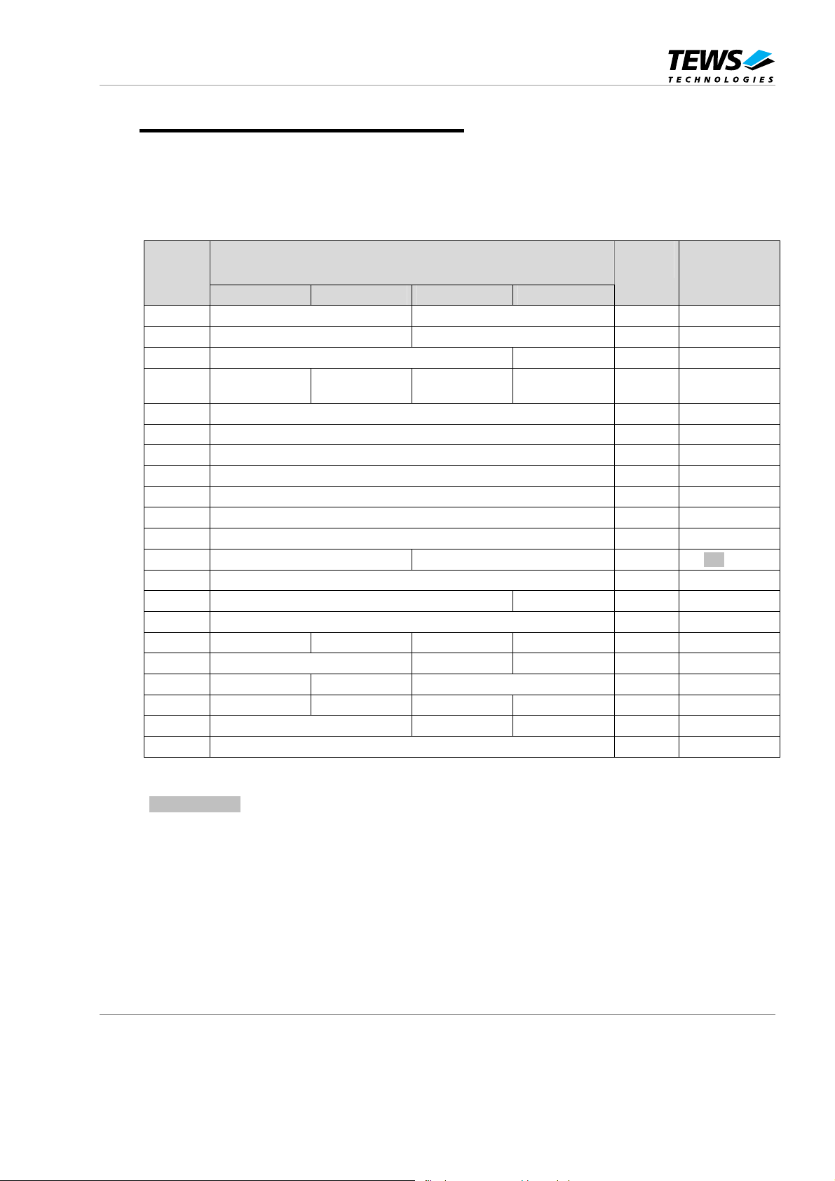
Write ‘0’ to all unused (Reserved) bits PCI CFG
Register
Address
0x00 Device ID Vendor ID N 029F 1498
0x04 Status Command Y 0280 0000
0x08 Class Code Revision ID N 118000 00
0x0C BIST Header Type
0x10 PCI Base Address 0 for MEM Mapped Config . Registers Y FFFFFF80
0x14 PCI Base Address 1 for I/O Mapped Config. Registers Y FFFFFF81
0x18 PCI Base Address 2 for Local Address Space 0 Y FFFFFFF1
0x1C PCI Base Address 3 for Local Address Space 1 Y 00000000
0x20 PCI Base Address 4 for Local Address Space 2 Y 00000000
0x24 PCI Base Address 5 for Local Address Space 3 Y 00000000
0x28 PCI Cardbus Information Structure Pointer N 00000000
0x2C Subsystem ID Subsystem Vendor ID N s.b. 1498
0x30 PCI Base Address for Local Expansion ROM Y 00000000
0x34 Reserved New Cap. Ptr. N 000000 40
0x38 Reserved N 00000000
0x3C Max_Lat Min_Gnt Interrupt Pin Interrupt Line Y[7:0] 00 00 01 00
0x40 PM Cap. PM Nxt Cap. PM Cap. ID N 4801 00 01
0x44 PM Data PM CSR EXT PM CSR Y 00 00 0000
0x48 Reserved HS CSR HS Nxt Cap. HS Cap. ID Y[23:16] 00 00 00 06
0x4C VPD Address VPD Nxt Cap. VPD Cap. ID Y[31:16] 0000 00 03
0x50 VPD Data Y 00000000
31 24 23 16 15 8 7 0
PCI Latency
Timer
Cache Line
Size
PCI
writeable
Y[7:0] 00 00 00 00
Initial Values
(Hex Values)
Figure 5-1 : PCI9030 Header
Subsystem ID: TPMC671-10: 0x000A
TPMC671-11: 0x000B
TPMC671-20: 0x0014
TPMC671-21: 0x0015
TPMC671 User Manual Issue 1.1 Page 19 of 28
Page 20
5.1.2 PCI Base Address Initialization
PCI Base Address Initialization is scope of the PCI host software.
PCI9030 PCI Base Address Initialization:
1. Write 0xFFFF_FFFF to the PCI9030 PCI Base Address Register.
2. Read back the PCI9030 PCI Base Address Register.
3. For PCI Base Address Registers 0:5, check bit 0 for PCI Address Space:
Bit 0 = '0' requires PCI Memory Space mapping
Bit 0 = '1' requires PCI I/O Space mapping
For the PCI Expansion ROM Base Address Register, check bit 0 for usage:
Bit 0 = ‘0’: Expansion ROM not used
Bit 0 = ‘1’: Expansion ROM used
4. For PCI I/O Space mapping, starting at bit location 2, the first bit set determines the size of the
required PCI I/O Space size.
For PCI Memory Space mapping, starting at bit location 4, the first bit set to '1' determines the size
of the required PCI Memory Space size.
For PCI Expansion ROM mapping, starting at bit location 11, the first bit set to '1' determines the
required PCI Expansion ROM size.
For example, if bit 5 of a PCI Base Address Register is detected as the first bit set to ‘1’, the
PCI9030 is requesting a 32 byte space (address bits 4:0 are not part of base address decoding).
5. Determine the base address and write the base address to the PCI9030 PCI Base Address
Register. For PCI Memory Space mapping the mapped address region must comply with the
definition of bits 3:1 of the PCI9030 PCI Base Address Register.
After programming the PCI9030 PCI Base Address Registers, the software must enable the
PCI9030 for PCI I/O and/or PCI Memory Space access in the PCI9030 PCI Command Register
(Offset 0x04). To enable PCI I/O Space access to the PCI9030, set bit 0 to '1'. To enable PCI
Memory Space access to the PCI9030, set bit 1 to '1'.
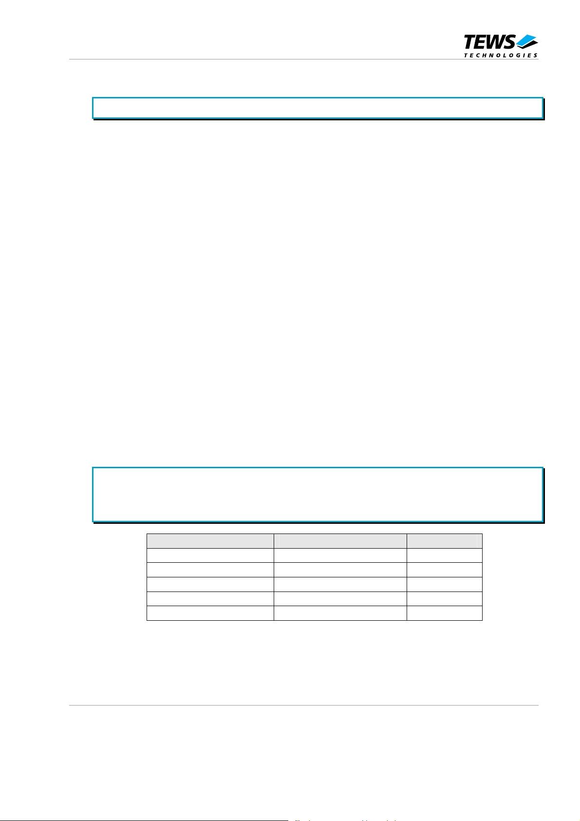
Offset in Config. Description Usage
0x10 PCI9030 LCR’s MEM Used
0x14 PCI9030 LCR’s I/O Used
0x18 PCI9030 Local Space 0 Used
0x1C PCI9030 Local Space 1 Not used
0x30 Expansion ROM Not used
Figure 5-2 : PCI9030 PLD Base Address Usage
TPMC671 User Manual Issue 1.1 Page 20 of 28
Page 21

5.2 Local Configuration Register (LCR)
After reset, the PCI9030 Local Configuration Registers are loaded from the on board serial
configuration EEPROM.
The PCI base address for the PCI9030 Local Configuration Registers is PCI9030 PCI Base
Address 0 (PCI Memory Space) (Offset 0x10 in the PCI9030 PCI Configuration Register Space)
or PCI9030 PCI Base Address 1 (PCI I/O Space) (Offset 0x14 in the PCI9030 PCI Configuration
Register Space).
Do not change hardware dependent bit settings in the PCI9030 Local Configuration Registers.
Offset from
PCI Base
Address
0x00 Local Address Space 0 Range 0x0FFF_FFF1
0x04 Local Address Space 1 Range 0x0000_0000
0x08 Local Address Space 2 Range 0x0000_0000
0x0C Local Address Space 3 Range 0x0000_0000
0x10 Local Exp. ROM Range 0x0000_0000
0x14 Local Re-map Register Space 0 0x0000_0001
0x18 Local Re-map Register Space 1 0x0000_0000
0x1C Local Re-map Register Space 2 0x0000_0000
0x20 Local Re-map Register Space 3 0x0000_0000
0x24 Local Re-map Register ROM 0x0000_0000
0x28 Local Address Space 0 Descriptor 0x0171_78A0
0x2C Local Address Space 1 Descriptor 0x0000_0000
0x30 Local Address Space 2 Descriptor 0x0000_0000
0x34 Local Address Space 3 Descriptor 0x0000_0000
0x38 Local Exp. ROM Descriptor 0x0000_0000
0x3C Chip Select 0 Base Address 0x0000_0009
0x40 Chip Select 1 Base Address 0x0000_0000
0x44 Chip Select 2 Base Address 0x0000_0000
0x48 Chip Select 3 Base Address 0x0000_0000
0x4C Interrupt Control/Status 0x0041
0x4E EEPROM Write Protect Boundary 0x0030
0x50 Miscellaneous Control Register 0x0078_0000
0x54 General Purpose I/O Control 0x0249_2492
0x70 Hidden1 Power Management data select 0x0000_0000
0x74 Hidden 2 Power Management data scale 0x0000 _0000
Register Value
Figure 5-3 : PCI9030 Local Configuration Register
TPMC671 User Manual Issue 1.1 Page 21 of 28
Page 22

5.3 Configuration EEPROM
After power-on or PCI reset, the PCI9030 loads initial configuration register data from the on board
configuration EEPROM.
The configuration EEPROM contains the following configuration data:
• Address 0x00 to 0x27 : PCI9030 PCI Configuration Register Values
• Address 0x28 to 0x87 : PCI9030 Local Configuration Register Values
• Address 0x88 to 0xFF : Reserved
See the PCI9030 Manual for more information.
Address Offset
0x00 0x02 0x04 0x06 0x08 0x0A 0x0C 0x0E
0x00 0x029F 0x1498 0x0280 0x0000 0x1180 0x0000 s.b. 0x1498
0x10 0x0000 0x0040 0x0000 0x0100 0x4801 0x0001 0x0000 0x0000
0x20 0x0000 0x0006 0x0000 0x0003 0x0FFF 0xFFF1 0x0000 0x0000
0x30 0x0000 0x0000 0x0000 0x0000 0x0000 0x0000 0x0000 0x0001
0x40 0x0000 0x0000 0x0000 0x0000 0x0000 0x0000 0x0000 0x0000
0x50 0x0171 0x78A0 0x0000 0x0000 0x0000 0x0000 0x0000 0x0000
0x60 0x0000 0x0000 0x0000 0x0009 0x0000 0x0000 0x0000 0x0000
0x70 0x0000 0x0000 0x0030 0x0041 0x0078 0x0000 0x0249 0x2492
0x80 0x0000 0x0000 0x0000 0x0000 0xFFFF 0xFFFF 0xFFFF 0xFFFF
0x90 0xFFFF 0xFFFF 0xFFFF 0xFFFF 0xFFFF 0xFFFF 0xFFFF 0xFFFF
0xA0 0xFFFF 0xFFFF 0xFFFF 0xFFFF 0xFFFF 0xFFFF 0xFFFF 0xFFFF
0xB0 0xFFFF 0xFFFF 0xFFFF 0xFFFF 0xFFFF 0xFFFF 0xFFFF 0xFFFF
0xC0 0xFFFF 0xFFFF 0xFFFF 0xFFFF 0xFFFF 0xFFFF 0xFFFF 0xFFFF
0xD0 0xFFFF 0xFFFF 0xFFFF 0xFFFF 0xFFFF 0xFFFF 0xFFFF 0xFFFF
0xE0 0xFFFF 0xFFFF 0xFFFF 0xFFFF 0xFFFF 0xFFFF 0xFFFF 0xFFFF
0xF0 0xFFFF 0xFFFF 0xFFFF 0xFFFF 0xFFFF 0xFFFF 0xFFFF 0xFFFF
Figure 5-4 : Configuration EEPROM TPMC671-xx
Subsystem-ID Value (Offset 0x0C): TPMC671-10: 0x000A
TPMC671-11: 0x000B
TPMC671-20: 0x0014
TPMC671-21: 0x0015
TPMC671 User Manual Issue 1.1 Page 22 of 28
Page 23

5.4 Local Software Reset
The PCI9030 Local Reset Output LRESETo# is used to reset the on board local logic.
The PCI9030 local reset is active during PCI reset or if the PCI Adapter Software Reset bit is set in the
PCI9030 local configuration register CNTRL (offset 0x50).
CNTRL[30] PCI Adapter Software Reset:
Value of 1 resets the PCI9030 and issues a reset to the Local Bus (LRESETo# asserted). The
PCI9030 remains in this reset condition until the PCI Host clears this bit. The contents of the PCI9030
PCI and Local Configuration Registers are not reset. The PCI9030 PCI Interface is not reset.
TPMC671 User Manual Issue 1.1 Page 23 of 28
Page 24
6 Configuration Hints
6.1 Software Reset (Controller and LRESET#)
A host on the PCI bus can set the software reset bit in the Miscellaneous Control Register (CNTRL;
0x50) of the PCI Controller PCI9030 to reset the Controller and assert LRESET# output. The PCI9030
remains in this reset condition until the PCI host clears the software reset bit.
6.2 Big / Little Endian
• PCI – Bus ( Little Endian )
Byte 0 AD[7..0]
Byte 1 AD[15..8]
Byte 2 AD[23..16]
Byte 3 AD[31..24]
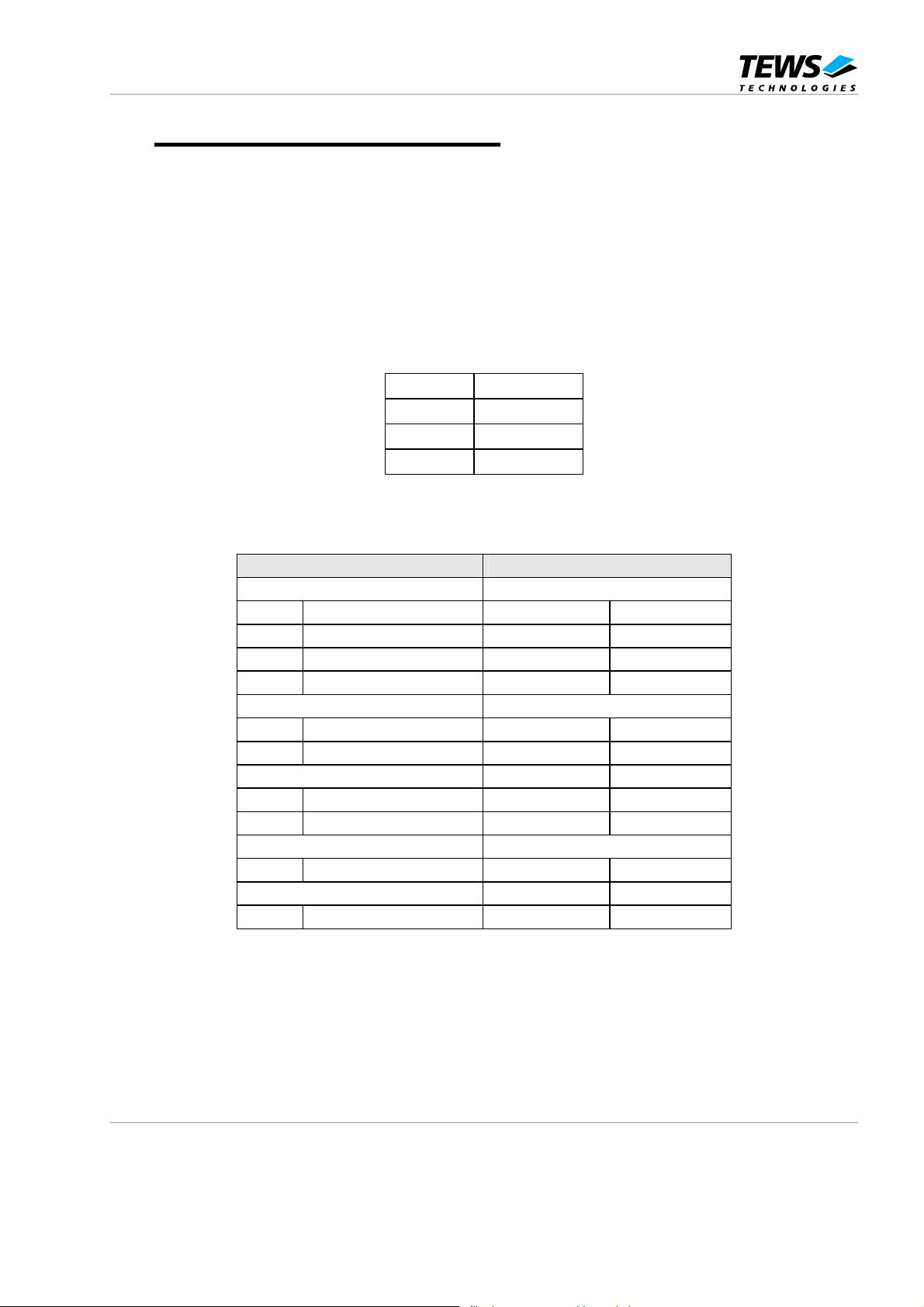
• Every Local Address Space (0...3) and the Expansion ROM Space can programmed to operate in
Big or Little Endian Mode.
Big Endian Little Endian
32 Bit 32 Bit
Byte 0 D[31..24] Byte 0 D[7..0]
Byte 1 D[23..16] Byte 1 D[15..8]
Byte 2 D[15..8] Byte 2 D[23..16]
Byte 3 D[7..0] Byte 3 D[31..24]
16 Bit upper lane 16 Bit
Byte 0 D[31..24] Byte 0 D[7..0]
Byte 1 D[23..16] Byte 1 D[15..8]
16 Bit lower lane
Byte 0 D[15..8]
Byte 1 D[7..0]
8 Bit upper lane 8 Bit
Byte 0 D[31..24] Byte 0 D[7..0]
8 Bit lower lane
Byte 0 D[7..0]
Figure 6-1 : Local Bus Little/Big Endian
TPMC671 User Manual Issue 1.1 Page 24 of 28
Page 25

Standard use of the TPMC671:
Local Address Space 0 16 bit bus in Big Endian Mode
Local Address Space 1 not used
Local Address Space 2 not used
Local Address Space 3 not used
Expansion ROM Space not used
To change the Endian Mode use the Local Configuration Registers for the corresponding Space. Bit
24 of the according register sets the Mode. A value of 1 indicates Big Endian and a value of 0
indicates Little Endian.
For further information please refer to the PCI9030 manual which is also part of the TPMC671-ED
Engineering Documentation.
Use the PCI Base Address 0 + Offset or PCI Base Address 1 + Offset:
Short cut Offset Name
LAS0BRD 0x28 Local Address Space 0 Bus Region Description Register
LAS1BRD 0x2C Local Address Space 0 Bus Region Description Register
LAS2BRD 0x30 Local Address Space 0 Bus Region Description Register
LAS3BRD 0x34 Local Address Space 0 Bus Region Description Register
EROMBRD 0x38 Expansion ROM Bus Region Description Register
You could also use the PCI - Base Address 1 I/O Mapped Configuration Registers.
TPMC671 User Manual Issue 1.1 Page 25 of 28
Page 26
7 Installation
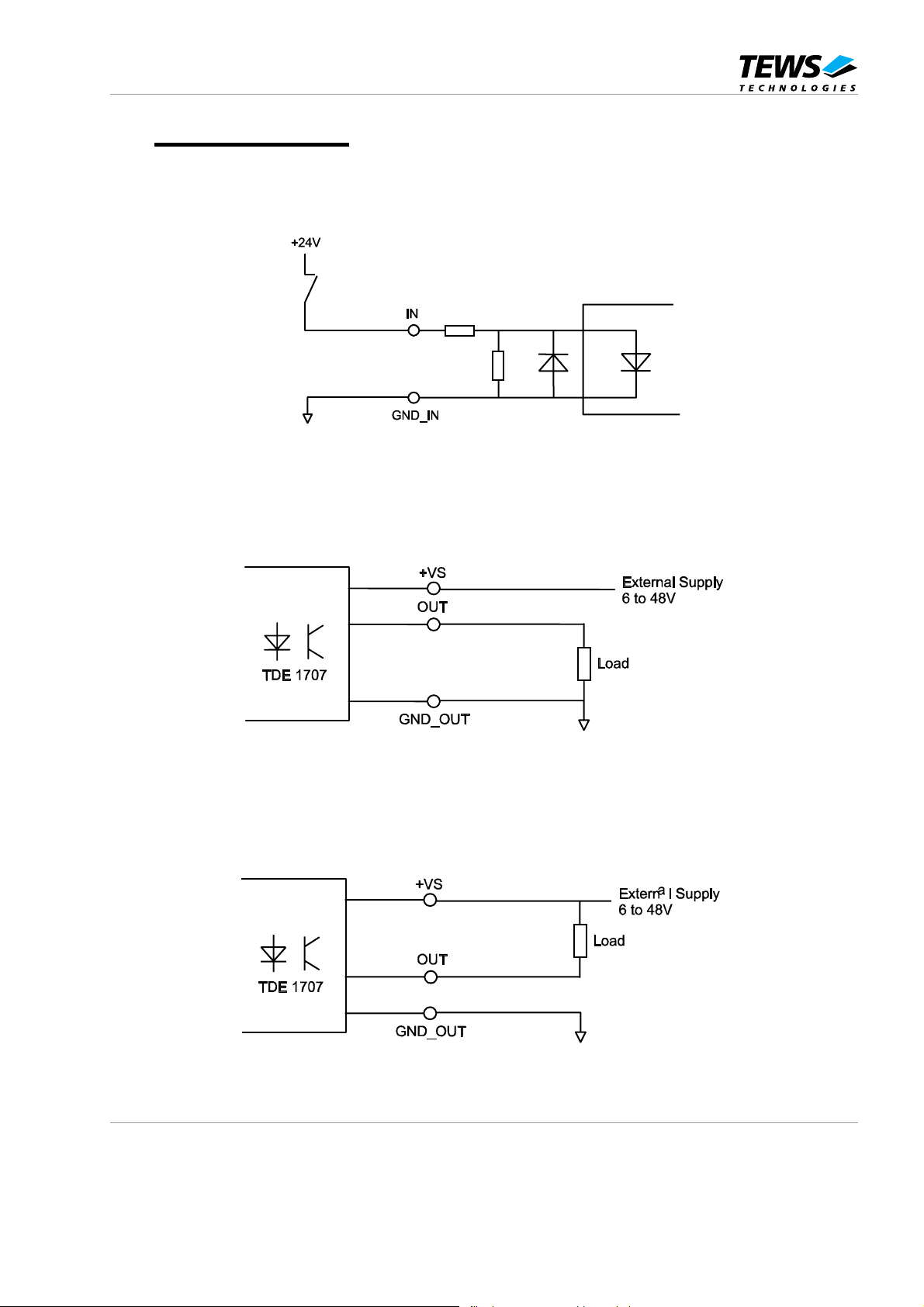
7.1 Input Wiring
Figure 7-1 : Input Wiring
7.2 Output Wiring High Side Switch (-10 / -20)
Figure 7-2 : Output Wiring High Side Switch
7.3 Output Wiring Low Side Switch (-11 / -21)
Figure 7-3 : Output Wiring Low Side Switch
TPMC671 User Manual Issue 1.1 Page 26 of 28
Page 27

8 Pin Assignment – I/O Connector
8.1 Front Panel Connector
Pin Signal Description Pin Signal Description
1 OUT 1 Output Line 1 35 VS_O2 External Supply OUT5 .. OUT8
2 OUT 2 Output Line 2 36 VS_O2 External Supply OUT5 .. OUT8
3 OUT 3 Output Line 3 37 VS_O3 External Supply OUT9 .. OUT12
4 OUT 4 Output Line 4 38 VS_O3 External Supply OUT9 .. OUT12
5 OUT 5 Output Line 5 39 VS_O4 External Supply OUT13 .. OUT16
6 OUT 6 Output Line 6 40 VS_O4 External Supply OUT13 .. OUT16
7 OUT 7 Output Line 7 41 GND_O1 Ground OUT 1 .. OUT 4
8 OUT 8 Output Line 8 42 GND_O1 Ground OUT 1 .. OUT 4
9 OUT 9 Output Line 9 43 GND_O2 Ground OUT 5 .. OUT 8
10 OUT 10 Output Line 10 44 GND_O2 Ground OUT 5 .. OUT 8
11 OUT 11 Output Line 11 45 GND_O3 Ground OUT 9 .. OUT 12
12 OUT 12 Output Line 12 46 GND_O3 Ground OUT 9 .. OUT 12
13 OUT 13 Output Line 13 47 GND_O4 Ground OUT 13 .. OUT 16
14 OUT 14 Output Line 14 48 GND_O4 Ground OUT 13 .. OUT 16
15 OUT 15 Output Line 15 49 IN 1- Ground IN 1
16 OUT 16 Output Line 16 50 IN 2- Ground IN 2
17 IN 1+ Input Line 1 51 IN 3- Ground IN 3
18 IN 2+ Input Line 2 52 IN 4- Ground IN 4
19 IN 3+ Input Line 3 53 IN 5- Ground IN 5
20 IN 4+ Input Line 4 54 IN 6- Ground IN 6
21 IN 5+ Input Line 5 55 IN 7- Ground IN 7
22 IN 6+ Input Line 6 56 IN 8- Ground IN 8
23 IN 7+ Input Line 7 57 IN 9- Ground IN 9
24 IN 8+ Input Line 8 58 IN 10- Ground IN 10
25 IN 9+ Input Line 9 59 IN 11- Ground IN 11
26 IN 10+ Input Line 10 60 IN 12- Ground IN 12
27 IN 11+ Input Line 11 61 IN 13- Ground IN 13
28 IN 12+ Input Line 12 62 IN 14- Ground IN 14
29 IN 13+ Input Line 13 63 IN 15- Ground IN 15
30 IN 14+ Input Line 14 64 IN 16- Ground IN 16
31 IN 15+ Input Line 15 65 n.c. Not Used
32 IN 16+ Input Line 16 66 n.c. Not Used
33 VS_O1 External Supply OUT1 .. OUT4 67 n.c. Not Used
34 VS_O1 External Supply OUT1 .. OUT4 68 n.c. Not Used
Figure 8-1 : Pin Assignment I/O HD68 SCSI-3 type Connector
Please check the maximum current of the used connection cable. Some standard cables
(AWG28 68pin) are limited to 0.75 A per lead.
TPMC671 User Manual Issue 1.1 Page 27 of 28
Page 28

8.2 Mezzanine Card Connector P14
Pin Signal Description Pin Signal Description
1 OUT 1 Output Line 1 2 OUT 2 Output Line 2
3 OUT 3 Output Line 3 4 OUT 4 Output Line 4
5 OUT 5 Output Line 5 6 OUT 6 Output Line 6
7 OUT 7 Output Line 7 8 OUT 8 Output Line 8
9 OUT 9 Output Line 9 10 OUT 10 Output Line 10
11 OUT 11 Output Line 11 12 OUT 12 Output Line 12
13 OUT 13 Output Line 13 14 OUT 14 Output Line 14
15 OUT 15 Output Line 15 16 OUT 16 Output Line 16
17 IN 1+ Input Line 1 18 IN 2+ Input Line 2
19 IN 3+ Input Line 3 20 IN 4+ Input Line 4
21 IN 5+ Input Line 5 22 IN 6+ Input Line 6
23 IN 7+ Input Line 7 24 IN 8+ Input Line 8
25 IN 9+ Input Line 9 26 IN 10+ Input Line 10
27 IN 11+ Input Line 11 28 IN 12+ Input Line 12
29 IN 13+ Input Line 13 30 IN 14+ Input Line 14
31 IN 15+ Input Line 15 32 IN 16+ Input Line 16
33 VS_O1 External Supply OUT1 .. OUT4 34 VS_O1 External Supply OUT1 .. OUT4
35 VS_O2 External Supply OUT5 .. OUT8 36 VS_O2 External Supply OUT5 .. OUT8
37 VS_O3 External Supply OUT9 .. OUT12 38 VS_O3 External Supply OUT9 .. OUT12
39 VS_O4 External Supply OUT13 .. OUT16 40 VS_O4 External Supply OUT13 .. OUT16
41 GND_O1 Ground OUT 1 .. OUT 4 42 GND_O1 Ground OUT 1 .. OUT 4
43 GND_O2 Ground OUT 5 .. OUT 8 44 GND_O2 Ground OUT 5 .. OUT 8
45 GND_O3 Ground OUT 9 .. OUT 12 46 GND_O3 Ground OUT 9 .. OUT 12
47 GND_O4 Ground OUT 13 .. OUT 16 48 GND_O4 Ground OUT 13 .. OUT 16
49 IN 1- Ground IN 1 50 IN 2- Ground IN 2
51 IN 3- Ground IN 3 52 IN 4- Ground IN 4
53 IN 5- Ground IN 5 54 IN 6- Ground IN 6
55 IN 7- Ground IN 7 56 IN 8- Ground IN 8
57 IN 9- Ground IN 9 58 IN 10- Ground IN 10
59 IN 11- Ground IN 11 60 IN 12- Ground IN 12
61 IN 13- Ground IN 13 62 IN 14- Ground IN 14
63 IN 15- Ground IN 15 64 IN 16- Ground IN 16
Figure 8-2 : Mezzanine Card Connector P14
Please verify that the tracks from the P14 connector to the Px connector of the PMC carrier
board are designed for a current of typical 0.5 A min per output.
TPMC671 User Manual Issue 1.1 Page 28 of 28
 Loading...