

Page 1

The Embedded I/O Compan
y
TPMC310
Conduction Cooled PMC
Isolated 2 x CAN Bus
Version 1.1
User Manual
Issue 1.1.5
January 2011
TEWS TECHNOLOGIES GmbH
Am Bahnhof 7 25469 Halstenbek, Germany
Phone: +49 (0) 4101 4058 0 Fax: +49 (0) 4101 4058 19
e-mail: [email protected]
www.tews.com
Page 2

TPMC310 User Manual Issue 1.1.5 Page 2 of 22
TPMC310-10
Conduction Cooled PMC, isolated 2 x CAN Bus,
P14 back I/O
This document contains information, which is
proprietary to TEWS TECHNOLOGIES GmbH. Any
reproduction without written permission is forbidden.
TEWS TECHNOLOGIES GmbH has made any
effort to ensure that this manual is accurate and
complete. However TEWS TECHNOLOGIES GmbH
reserves the right to change the product described
in this document at any time without notice.
TEWS TECHNOLOGIES GmbH is not liable for any
damage arising out of the application or use of the
device described herein.
Style Conventions
Hexadecimal characters are specified with prefix 0x,
i.e. 0x029E (that means hexadecimal value 029E).
For signals on hardware products, an ‚Active Low’ is
represented by the signal name with # following, i.e.
IP_RESET#.
Access terms are described as:
W Write Only
R Read Only
R/W Read/Write
R/C Read/Clear
R/S Read/Set
©2003-2011 by TEWS TECHNOLOGIES GmbH
All trademarks mentioned are property of their
respective owners.
Page 3

TPMC310 User Manual Issue 1.1.5 Page 3 of 22
Issue Description Date
1.0 Initial Issue October 2003
1.1 CAN Oscillator Frequency corrected (16 MHz) June 2004
1.2 New address TEWS LLC September 2006
1.3
Minor Version Step,
New PCB,
Added secondary thermal interface,
Added extra mounting holes preventing vibration,
MTBF value has changed,
Solder pad locations for termination options have changed.
April 2008
1.1.4 New Notation for User Manual and Engineering Documentation December 2008
1.1.5
(1) Corrected I/O Line Configuration Table
(2) Added note for the Bus_End Option
(3) Added note for supported baud rate range to Technical
Specification Table
January 2011
Page 4

TPMC310 User Manual Issue 1.1.5 Page 4 of 22
Table of Contents
1 PRODUCT DESCRIPTION.........................................................................................5
2 TECHNICAL SPECIFICATION...................................................................................7
3 LOCAL SPACE ADDRESSING..................................................................................8
3.1 PCI9030 Local Space Configuration .............................................................................................8
3.2 PLD Register Space........................................................................................................................8
3.2.1 CAN Control Register...........................................................................................................9
3.2.2 CAN Status Register...........................................................................................................10
3.2.3 CAN Controller Register Space..........................................................................................11
4 PCI9030 TARGET CHIP...........................................................................................12
4.1 PCI Configuration Registers (PCR).............................................................................................12
4.1.1 PCI9030 PCI Header..........................................................................................................12
4.1.2 PCI Base Address Initialization ..........................................................................................13
4.2 Local Configuration Register (LCR)............................................................................................14
4.3 Configuration EEPROM................................................................................................................15
4.4 Local Software Reset....................................................................................................................16
5 PROGRAMMING HINTS .......................................................................................... 17
5.1 CAN Controller (SJA1000)............................................................................................................17
6 CONFIGURATION HINTS........................................................................................19
6.1 I/O Line Configuration ..................................................................................................................19
6.2 Solder Pad Location .....................................................................................................................20
7 PIN ASSIGNMENT...................................................................................................21
Page 5

TPMC310 User Manual Issue 1.1.5 Page 5 of 22
List of Figures
FIGURE 1-1 : BLOCK DIAGRAM......................................................................................................................6
FIGURE 6-1 : SOLDER PAD LOCATION.......................................................................................................20
List of Tables
TABLE 2-1 : TECHNICAL SPECIFICATION.....................................................................................................7
TABLE 3-1 : PCI9030 LOCAL SPACE CONFIGURATION ..............................................................................8
TABLE 3-2 : PLD REGISTER SPACE..............................................................................................................8
TABLE 3-3 : CAN CONTROL REGISTER........................................................................................................9
TABLE 3-4 : CAN STATUS REGISTER..........................................................................................................10
TABLE 3-5 : CAN CONTROLLER REGISTER SPACE..................................................................................11
TABLE 4-1 : PCI9030 PCI HEADER...............................................................................................................12
TABLE 4-2 : PCI9030 LOCAL CONFIGURATION REGISTER......................................................................14
TABLE 4-3 : CONFIGURATION EEPROM.....................................................................................................15
TABLE 5-1 : OUTPUT CONTROL REGISTER...............................................................................................17
TABLE 5-2 : CLOCK DIVIDER REGISTER ....................................................................................................18
TABLE 6-1 : I/O LINE CONFIGURATION......................................................................................................19
TABLE 6-2 : FACTORY DEFAULT I/O LINE CONFIGURATION...................................................................19
TABLE 7-1 : P14 I/O PIN ASSIGNMENT........................................................................................................22
Page 6
TPMC310 User Manual Issue 1.1.5 Page 6 of 22
1 Product Description
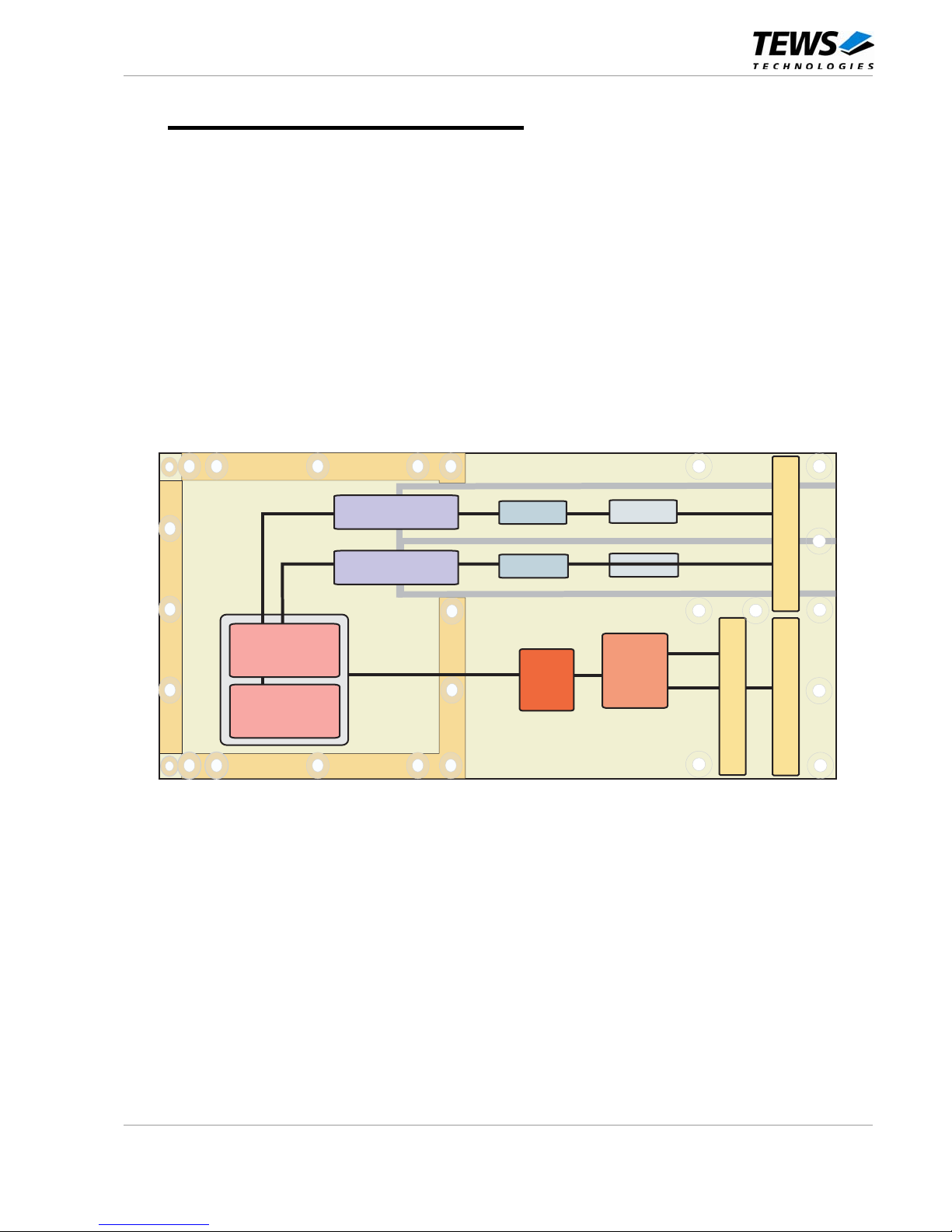
The TPMC310 is a conduction cooled single-width 32 bit PMC module providing a two channel high
speed CAN bus interface.
The PLX Technology PCI9030 PCI Target Chip is used for the PCI bus interface.
Two Philips SJA1000 CAN Controllers (CAN specification 2.0B supported) are used for the CAN bus
interface (one for each channel).
The CAN bus I/O interface provides two independent channels, isolated from system logic and from
each other.
CAN High Speed transceivers are used for the CAN bus I/O interface.
An on board termination option (solder pads) is provided for each CAN bus channel allowing to
configure on board termination and/or pass trough mode for the CAN bus.
The TPMC310 uses the P14 I/O connector for the CAN bus I/O interface.
P11
P12
PCI9030
PCI Target
Chip
PLD
Logic
CAN CH2
Transceiver
CAN CH2
Power & Signal Isolation
CAN CH2
Term. Opt.
CAN CH1
Term. Opt.
SJA1000
CAN
Controller
SJA1000
CAN
Controller
CAN CH1
Power & Signal Isolation
CAN CH1
Transceiver
P14
Figure 1-1 : Block Diagram
Page 7

TPMC310 User Manual Issue 1.1.5 Page 7 of 22
2 Technical Specification
Logic Interface
Mechanical Interface
PCI Mezzanine Card (PMC) Interface
Conduction Cooled
Single Size
Electrical Interface
PCI Rev. 2.1 compliant
33 MHz / 32 bit PCI
Universal PCI Signaling Voltage (3.3V PCI Signaling Voltage, 5V
PCI Signaling Voltage tolerant)
On board Devices
PCI Target Chip
PCI9030 (PLX Technology)
CAN Controller
2 x SJA1000 (Philips) (16 MHz)
CAN Bus Transceiver
2 x TJA1050 (Philips)
I/O Interface
Number of CAN Bus
Channels
2 (isolated from system logic and from each other)
CAN Bus Interface
CAN High Speed
The TJA1050 High-Speed CAN Transceiver supports baud rates
from 60 kbaud up to 1 Mbaud
I/O Connector
PMC P14 I/O (64pin Mezzanine Connector)
Physical Data
Power Requirements
50mA typ @ + 3.3V DC
150mA typ @ + 5.0V DC
Temperature Range
Operating :
Storage :
-40°C to + 85°C
-55°C to +125°C
MTBF
372000 h
Weight
75g
Humidity
5 – 95 % non-condensing
Table 2-1 : Technical Specification
Page 8
TPMC310 User Manual Issue 1.1.5 Page 8 of 22
3 Local Space Addressing
3.1 PCI9030 Local Space Configuration
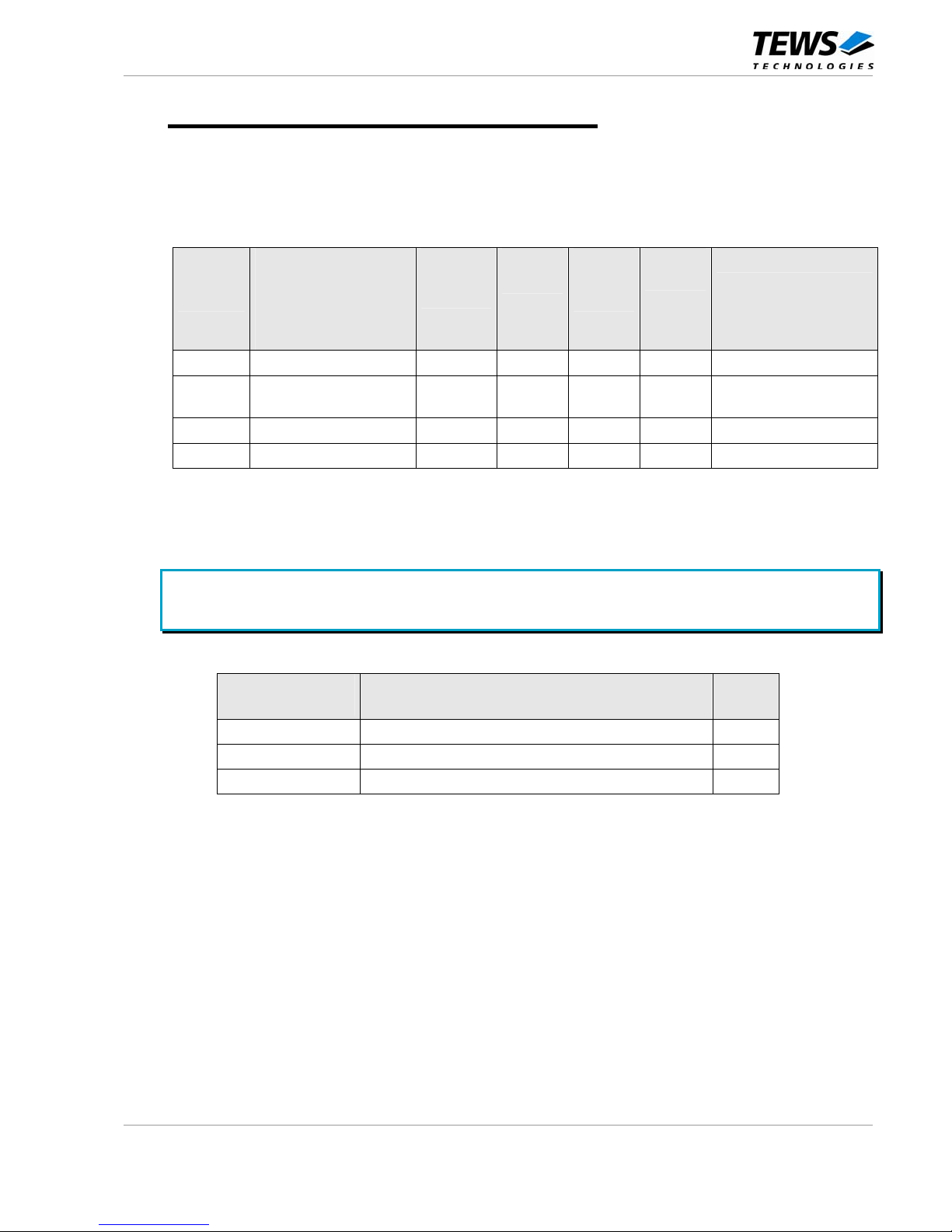
The local on board addressable regions are accessed from the PCI side by using the PCI9030 local
spaces.
PCI9030
Local
Space
PCI9030
PCI Base Address
(Offset in PCI
Configuration
Space)
PCI
Space
Mapping
Size
(Byte)
Port
Width
(Bit)
Endian
Mode
Description
0 2 (0x18) MEM 16 8 BIG PLD Register Space
1 3 (0x1C) MEM 512 8 BIG
CAN Controller
Register Space
2 4 (0x20) - - - - Not Used
3 5 (0x24) - - - - Not Used
Table 3-1 : PCI9030 Local Space Configuration
3.2 PLD Register Space
PCI Base Address :
PCI9030 PCI Base Address 2 (Offset 0x18 in PCI9030 PCI Configuration Register Space)
Offset to PCI
Base Address
Register Name Size
(Bit)
0x00 CAN CONTROL REGISTER 8
0x01 CAN STATUS REGISTER 8
0x02 … 0x0F Reserved 8
Table 3-2 : PLD Register Space
Page 9

TPMC310 User Manual Issue 1.1.5 Page 9 of 22
3.2.1 CAN Control Register
Bit Name Function Access Reset
7 :6 - Reserved (Undefined for reads, write as '0') - X
5 CAN2_INTEN
0 : CAN CH2 Interrupt Disabled
1 : CAN CH2 Interrupt Enabled
R/W 0
4 CAN2_SEL
0 : CAN CH2 Transceiver Silent Mode
1 : CAN CH2 Transceiver Operating M ode
R/W 0
3 CAN2_RST#
0 : CAN CH2 Controller Reset Mode
1 : CAN CH2 Controller Operating Mode
R/W 0
2 CAN1_INTEN
0 : CAN CH1 Interrupt Disabled
1 : CAN CH1 Interrupt Enabled
R/W 0
1 CAN1_SEL
0 : CAN CH1 Transceiver Silent Mode
1 : CAN CH1 Transceiver Operating Mode
R/W 0
0 CAN1_RST#
0 : CAN CH1 Controller Reset Mode
1 : CAN CH1 Controller Operating Mode
R/W 0
Table 3-3 : CAN Control Register
After power-up or board reset the CAN controllers are set to reset mode.
To set the CAN controllers to operating mode, the CANx_RST# bit must be set to ‘1’.
After power-up or board reset the CAN bus transceivers are set to silent mode.
To set the CAN bus transceivers to operating mode, the CANx_SEL bit must be set to ‘1’.
Disabling interrupts in the CAN Control Register only affects the interrupt mapping to the
PCI9030 LINTx# local interrupt inputs. It will not affect the interrupt source of the SJA1000 CAN
controllers.
If enabled, the CAN CH1 interrupt source is mapped to the PCI9030 LINT1# local interrupt input.
If enabled, the CAN CH2 interrupt source is mapped to the PCI9030 LINT2# local interrupt input.
The PCI9030 LINTx# local interrupt inputs are used in active low level sensitive mode.
The CAN interrupts must be acknowledged via SJA1000 registers (CAN Controller Register
Space).
Please see the SJA1000 CAN Controller Manual for more information.
Page 10

TPMC310 User Manual Issue 1.1.5 Page 10 of 22
3.2.2 CAN Status Register
Bit Name Function Access Reset
7:2 - Reserved (Undefined for reads) - X
1 CAN2_INT CAN CH2 Controller Interrupt Request Status R X
0 CAN1_INT CAN CH1 Controller Interrupt Request Status R X
Table 3-4 : CAN Status Register
The CAN CHx controller interrupt request status is '0' for "no active interrupt request" and '1'
for "active interrupt request".
Please see the SJA1000 CAN Controller Manual for more information.
If enabled, the CAN CH1 interrupt source is mapped to the PCI9030 LINT1# local interrupt input.
If enabled, the CAN CH2 interrupt source is mapped to the PCI9030 LINT2# local interrupt input.
The PCI9030 LINTx# local interrupt inputs are used in active low level sensitive mode.
The CAN interrupts must be acknowledged via SJA1000 registers (CAN Controller Register
Space).
Please see the SJA1000 CAN Controller Manual for more information.
Page 11
TPMC310 User Manual Issue 1.1.5 Page 11 of 22
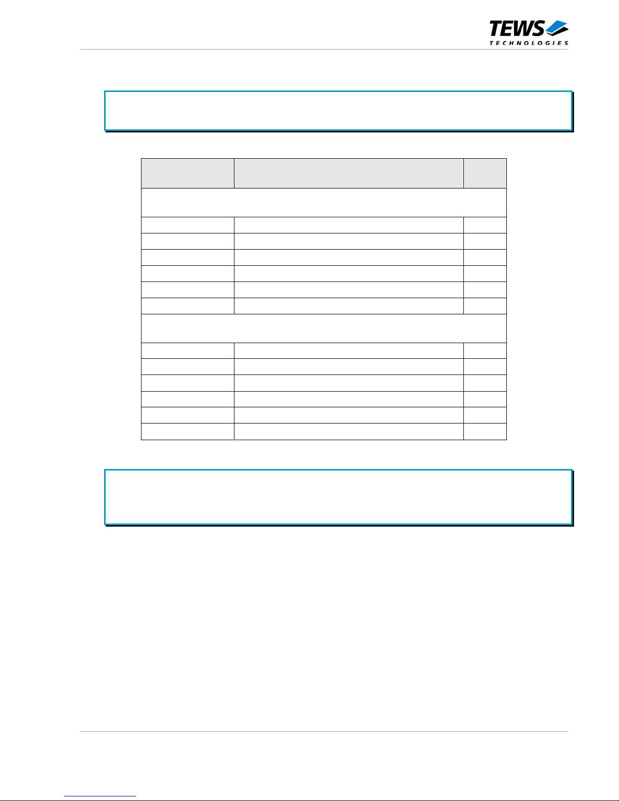
3.2.3 CAN Controller Register Space
PCI Base Address :
PCI9030 PCI Base Address 3 (Offset 0x1C in PCI9030 PCI Configuration Register Space).
Offset to PCI
Base Address
Register Name Size
(Bit)
CAN Controller Channel 1
0x000 CAN Controller CH1 Address 0 8
0x001 CAN Controller CH1 Address 1 8
0x002 CAN Controller CH1 Address 2 8
… … …
0x07F CAN Controller CH1 Address 127 (dec. ) 8
0x080 … 0x0FF Reserved -
CAN Controller Channel 2
0x100 CAN Controller CH2 Address 0 8
0x101 CAN Controller CH2 Address 1 8
0x102 CAN Controller CH2 Address 2 8
… … …
0x17F CAN Controller CH2 Address 127 (dec. ) 8
0x180 … 0x1FF Reserved -
Table 3-5 : CAN Controller Register Space
The CAN controllers must be set to operating mode (CAN Control Register in PLD Register
Space) before CAN controller register access.
Please see the SJA1000 CAN Controller Manual for a detailed register description.
Page 12
TPMC310 User Manual Issue 1.1.5 Page 12 of 22
4 PCI9030 Target Chip
4.1 PCI Configuration Registers (PCR)
4.1.1 PCI9030 PCI Header
Write ‘0’ to all unused (Reserved) bits
PCI CFG
Register
Address
31 24 23 16 15 8 7 0
PCI
writeable
Initial Values
(Hex Values)
0x00 Device ID Vendor ID N 0136 1498
0x04 Status Command Y 0280 0000
0x08 Class Code Revision ID N 028000 00
0x0C BIST Header Type
PCI Latency
Timer
Cache Line
Size
Y[7:0] 00 00 00 00
0x10 PCI Base Address 0 for MEM Mapped Config . Registers Y FFFFFF80
0x14 PCI Base Address 1 for I/O Mapped Config. Registers Y FFFFFF81
0x18 PCI Base Address 2 for Local Address Space 0 Y FFFFFFF0
0x1C PCI Base Address 3 for Local Address Space 1 Y FFFFFE00
0x20 PCI Base Address 4 for Local Address Space 2 Y 00000000
0x24 PCI Base Address 5 for Local Address Space 3 Y 00000000
0x28 PCI CardBus Information Structure Pointer N 00000000
0x2C Subsystem ID Subsystem Vendor ID N s.b. 1498
0x30 PCI Base Address for Local Expansion ROM Y 00000000
0x34 Reserved New Cap. Ptr. N 000000 40
0x38 Reserved N 00000000
0x3C Max_Lat Min_Gnt Interrupt Pin Interrupt Line Y[7:0] 00 00 01 00
0x40 PM Cap. PM Nxt Cap. PM Cap. ID N 4801 00 01
0x44 PM Data PM CSR EXT PM CSR Y 00 00 0000
0x48 Reserved HS CSR HS Nxt Cap. HS Cap. ID Y[23:16] 00 00 00 06
0x4C VPD Address VPD Nxt Cap. VPD Cap. ID Y[31:16] 0000 00 03
0x50 VPD Data Y 00000000
Table 4-1 : PCI9030 PCI Header
Subsystem-ID: TPMC310-10: 0x000A
Page 13

TPMC310 User Manual Issue 1.1.5 Page 13 of 22
4.1.2 PCI Base Address Initialization
PCI Base Address Initialization is scope of the PCI host software.
PCI9030 PCI Base Address Initialization:
1. Write 0xFFFF_FFFF to the PCI9030 PCI Base Address Register
2. Read back the PCI9030 PCI Base Address Register
3. For PCI Base Address Registers 0:5, check bit 0 for PCI Address Space:
Bit 0 = '0' requires PCI Memory Space mapping
Bit 0 = '1' requires PCI I/O Space mapping
For the PCI Expansion ROM Base Address Register, check bit 0 for usage:
Bit 0 = ‘0’: Expansion ROM not used
Bit 0 = ‘1’: Expansion ROM used
4. For PCI I/O Space mapping, starting at bit location 2, the first bit set determines the size of the
required PCI I/O Space size.
For PCI Memory Space mapping, starting at bit location 4, the first bit set to '1' determines the size
of the required PCI Memory Space size.
For PCI Expansion ROM mapping, starting at bit location 11, the first bit set to '1' determines the
required PCI Expansion ROM size.
For example, if bit 5 of a PCI Base Address Register is detected as the first bit set to ‘1’, the
PCI9030 is requesting a 32 byte space (address bits 4:0 are not part of base address decoding).
5. Determine the base address and write the base address to the PCI9030 PCI Base Address
Register. For PCI Memory Space mapping the mapped address region must comply with the
definition of bits 3:1 of the PCI9030 PCI Base Address Register.
After programming the PCI9030 PCI Base Address Registers, the host software must enable
the PCI9030 for PCI I/O and/or PCI Memory Space access in the PCI9030 PCI Command
Register (Offset 0x04):
To enable PCI I/O Space access to the PCI9030, bit 0 must be set to '1'.
To enable PCI Memory Space access to the PCI9030, bit 1 must be set to '1'.
Page 14

TPMC310 User Manual Issue 1.1.5 Page 14 of 22
4.2 Local Configuration Register (LCR)
After reset, the PCI9030 Local Configuration Registers are loaded from the on board serial
configuration EEPROM.
PCI Base Address :
PCI9030 PCI Base Address 0 (PCI Memory Space) (Offset 0x10 in PCI9030 PCI Configuration
Register Space), or
PCI9030 PCI Base Address 1 (PCI I/O Space) (Offset 0x14 in PCI9030 PCI Configuration
Register Space).
Do not change hardware dependent bit settings in the PCI9030 Local Configuration Registers.
Offset to PCI Base
Address
Register Value
0x00 Local Address Space 0 Range 0x0FFF_FFF0
0x04 Local Address Space 1 Range 0x0FFF_FE00
0x08 Local Address Space 2 Range 0x0000_0000
0x0C Local Address Space 3 Range 0x0000_0000
0x10 Local Exp. ROM Range 0x0000_0000
0x14 Local Re-map Register Space 0 0x0000_0001
0x18 Local Re-map Register Space 1 0x0000_1001
0x1C Local Re-map Register Space 2 0x0000_0000
0x20 Local Re-map Register Space 3 0x0000_0000
0x24 Local Re-map Register ROM 0x0000_0000
0x28 Local Address Space 0 Descriptor 0x1500_C0A0
0x2C Local Address Space 1 Descriptor 0x1502_4120
0x30 Local Address Space 2 Descriptor 0x0000_0000
0x34 Local Address Space 3 Descriptor 0x0000_0000
0x38 Local Exp. ROM Descriptor 0x0000_0000
0x3C Chip Select 0 Base Address 0x0000_0009
0x40 Chip Select 1 Base Address 0x0000_1081
0x44 Chip Select 2 Base Address 0x0000_1181
0x48 Chip Select 3 Base Address 0x0000_0000
0x4C Interrupt Control/Status 0x0049
0x4E EEPROM Write Protect Boundary 0x0030
0x50 Miscellaneous Control Register 0x0078_0000
0x54 General Purpose I/O Control 0x0224_9252
0x70 Hidden1 Power Management 0x0000_0000
0x74 Hidden 2 Power Management 0x0000_0000
Table 4-2 : PCI9030 Local Configuration Register
Page 15

TPMC310 User Manual Issue 1.1.5 Page 15 of 22
4.3 Configuration EEPROM
After power-on or PCI reset, the PCI9030 loads initial configuration register data from the on board
configuration EEPROM.
The configuration EEPROM contains the following configuration data:
• Address 0x00 to 0x27 : PCI9030 PCI Configuration Register Values
• Address 0x28 to 0x87 : PCI9030 Local Configuration Register Values
• Address 0x88 to 0xFF : Reserved
See the PCI9030 Manual for more information.
Address Offset
0x00 0x02 0x04 0x06 0x08 0x0A 0x0C 0x0E
0x00 0x0136 0x1498 0x0280 0x0000 0x0280 0x0000 s.b. 0x1498
0x10 0x0000 0x0040 0x0000 0x0100 0x4801 0x0001 0x0000 0x0000
0x20 0x0000 0x0006 0x0000 0x0003 0x0FFF 0xFFF0 0x0FFF 0xFE00
0x30 0x0000 0x0000 0x0000 0x0000 0x0000 0x0000 0x0000 0x0001
0x40 0x0000 0x1001 0x0000 0x0000 0x0000 0x0000 0x0000 0x0000
0x50 0x1500 0xC0A0 0x1502 0x4120 0x0000 0x0000 0x0000 0x0000
0x60 0x0000 0x0000 0x0000 0x0009 0x0000 0x1081 0x0000 0x1181
0x70 0x0000 0x0000 0x0030 0x0049 0x0078 0x0000 0x0224 0x9252
0x80 0x0000 0x0000 0x0000 0x0000 0xFFFF 0xFFFF 0xFFFF 0xFFFF
0x90 0xFFFF 0xFFFF 0xFFFF 0xFFFF 0xFFFF 0xFFFF 0xFFFF 0xFFFF
0xA0 0xFFFF 0xFFFF 0xFFFF 0xFFFF 0xFFFF 0xFFFF 0xFFFF 0xFFFF
0xB0 0xFFFF 0xFFFF 0xFFFF 0xFFFF 0xFFFF 0xFFFF 0xFFFF 0xFFFF
0xC0 0xFFFF 0xFFFF 0xFFFF 0xFFFF 0xFFFF 0xFFFF 0xFFFF 0xFFFF
0xD0 0xFFFF 0xFFFF 0xFFFF 0xFFFF 0xFFFF 0xFFFF 0xFFFF 0xFFFF
0xE0 0xFFFF 0xFFFF 0xFFFF 0xFFFF 0xFFFF 0xFFFF 0xFFFF 0xFFFF
0xF0 0xFFFF 0xFFFF 0xFFFF 0xFFFF 0xFFFF 0xFFFF 0xFFFF 0xFFFF
Table 4-3 : Configuration EEPROM
Subsystem-ID Value (EEPROM Offset 0x0C): TPMC310-10: 0x000A
Page 16

TPMC310 User Manual Issue 1.1.5 Page 16 of 22
4.4 Local Software Reset
The PCI9030 Local Reset Output LRESETo# is used to reset the on board local logic.
The PCI9030 local reset is active during PCI reset or if the PCI Adapter Software Reset bit is set in the
PCI9030 local configuration register CNTRL (offset 0x50).
CNTRL[30] PCI Adapter Software Reset:
Value of 1 resets the PCI9030 and issues a reset to the Local Bus (LRESETo# asserted). The
PCI9030 remains in this reset condition until the PCI Host clears this bit. The contents of the PCI9030
PCI and Local Configuration Registers are not reset. The PCI9030 PCI Interface is also not reset.
Page 17

TPMC310 User Manual Issue 1.1.5 Page 17 of 22
5 Programming Hints
5.1 CAN Controller (SJA1000)
Clock Source:
The SJA1000 clock input frequency is 16 MHz (for both SJA1000 CAN controllers).
Reset Mode:
After power-up or board reset the SJA1000 CAN controllers are held in “reset mode”.
To bring the SJA1000 CAN controllers out of reset mode, the CANx_RST# bit(s) in the CAN Control
Register (PLD Register Space) must be set.
Silent Mode:
After power-up or board reset the CAN bus transceivers are held in “silent mode”.
To bring the CAN bus transceivers to operating mode, the CANx_SEL bit(s) in the CAN Control
Register (PLD Register Space) must be set.
Output Control Register:
The SJA1000 Output Control Register must be programmed as follows (for both SJA1000 CAN
controllers in the SJA1000 controller internal reset mode - see SJA1000 Control Register in the
SJA1000 CAN Controller Manual):
Bit Symbol Description
7 OCTP1
6 OCTN1
11 : Push-Pull output stage
5 OCPOL1 0 : Normal polarity
4 OCTP0
3 OCTN0
11 : Push-Pull output stage
2 OCPOL0 0 : Normal polarity
1 OCMODE1
0 OCMODE0
01 : Test Output Mode
10 : Normal Output Mode
Table 5-1 : Output Control Register
Page 18

TPMC310 User Manual Issue 1.1.5 Page 18 of 22
Clock Divider Register:
The SJA1000 Clock Divider Register must be programmed as follows (for both SJA1000 CAN
controllers in the SJA1000 controller internal reset mode - see SJA1000 Control Register in the
SJA1000 CAN Controller Manual):
Bit Symbol Description
7 CAN MODE
0 : BasiCAN Mode
1 : PeliCAN Mode
6 CBP 1 : Bypass input comparator, use RX0 only
5 RXINTEN 0 : Disable Interrupts on TX1 output
4 - 0
3 CLOCK OFF 1 : Disable Clock Output (not used)
2 CD2 0
1 CD1 0
0 CD0 0
Table 5-2 : Clock Divider Register
Baud Rate Range:
The TPMC310 uses the TJA1050 High-Speed CAN transceiver.
The TJA1050 High-Speed CAN Transceiver supports baud rates from 60 kbaud up to 1 Mbaud.
Page 19

TPMC310 User Manual Issue 1.1.5 Page 19 of 22
6 Configuration Hints
6.1 I/O Line Configuration
The I/O line configuration is configured by on board solder pads (there is no jumper solution because
the TPMC310 is considered to be used in a vibration-sensitive environment).
Possible line configuration options for each of the two I/O channels (CAN CH1, CAN CH2) are:
• On board Termination Mode : on / off
• Bus Mode : bus_end / pass_through
The on board termination option for a CAN I/O channel node input (see P14 I/O pin assignment) is a
120 ohm split termination network.
For the bus_end option, the I/O lines are NOT passed through from the node input pins to the node
output pins of the P14 I/O connector. The node input pins must be used to connect the CAN bus lines
(see P14 I/O pin assignment).
For the pass_through option, the I/O lines are passed through from the node input pins to the node
output pins of the P14 I/O connector (see P14 I/O pin assignment).
Termination Mode Bus Mode
On board
Termination On
On board
Termination Off
Bus_End Pass_Through
CAN CH1 R42, R43 Closed R42, R43 Open R35, R45 Open R35, R45 Closed
CAN CH2 R37, R38 Closed R37, R38 Open R33, R40 Open R33, R40 Closed
Table 6-1 : I/O Line Configuration
Termination Mode Bus Mode
CAN CH1 On Bus_End
CAN CH2 On Bus_End
Table 6-2 : Factory Default I/O Line Configuration
Page 20
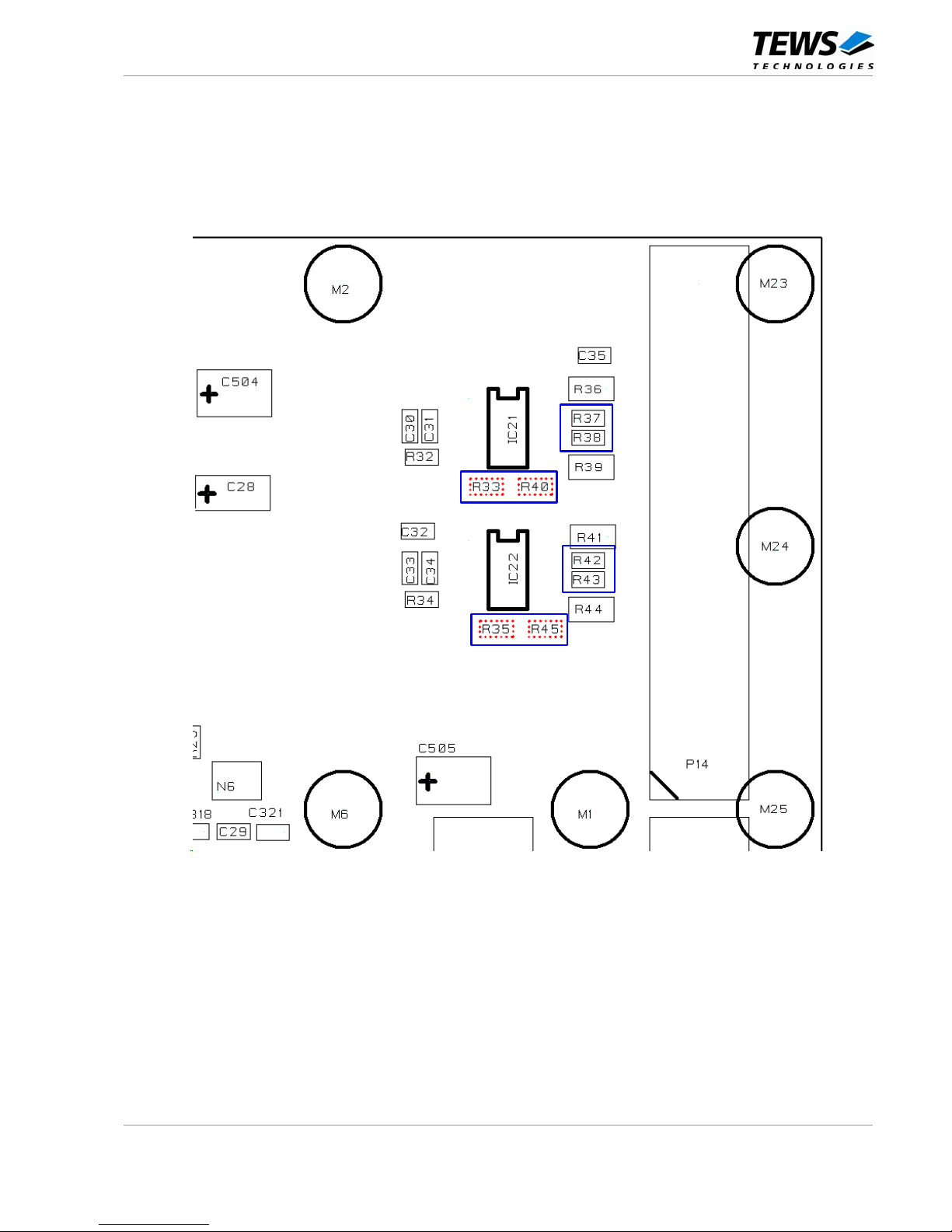
TPMC310 User Manual Issue 1.1.5 Page 20 of 22
6.2 Solder Pad Location
TPMC310 PCB, Top View, Upper Right Corner
Figure 6-1 : Solder Pad Location
Page 21

TPMC310 User Manual Issue 1.1.5 Page 21 of 22
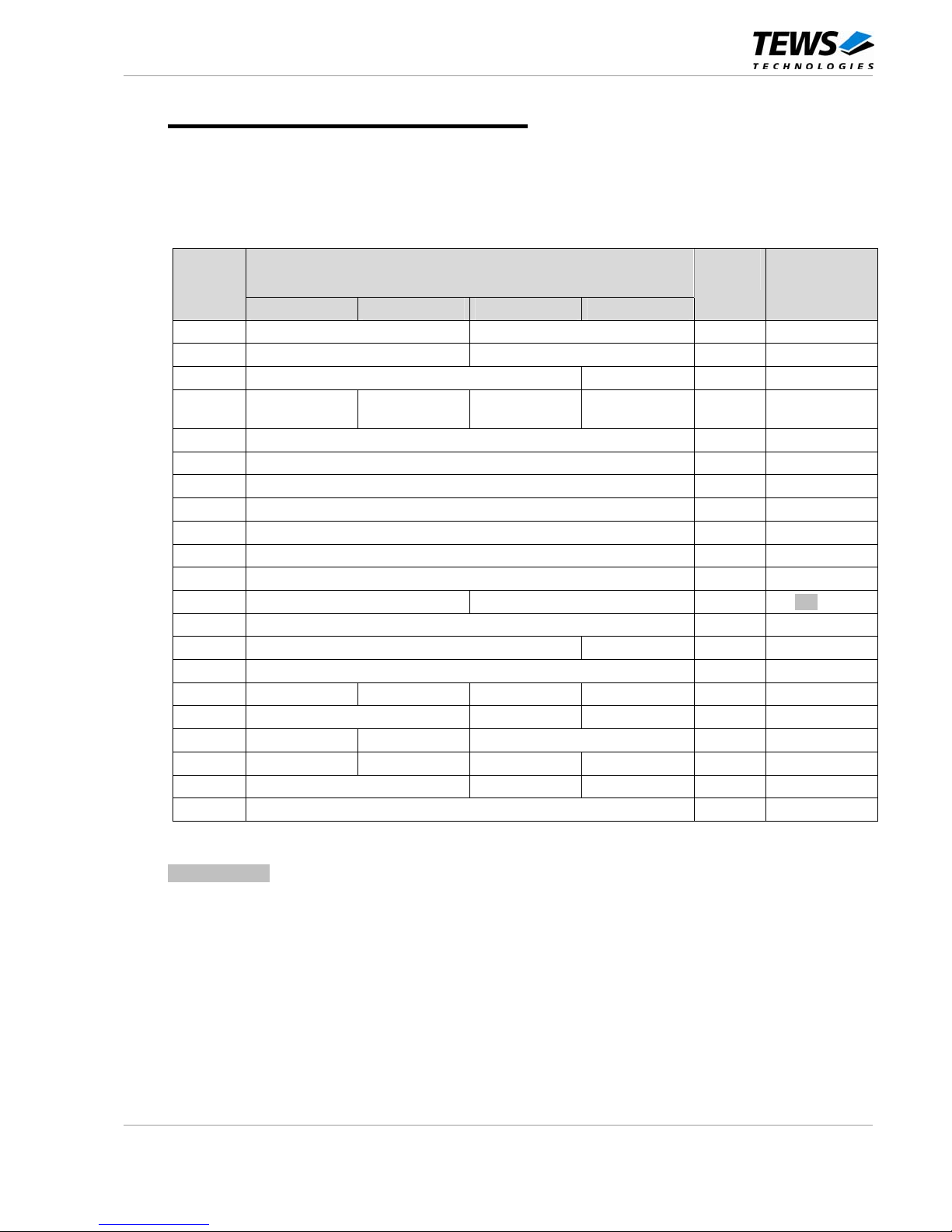
7 Pin Assignment
The complete TPMC310 I/O interface is available on the 64 pin P14 mezzanine connector ("back I/O").
Pin Signal Interface
Bus_End
Option
Pass_Through
Option
1 Reserved
2 Reserved
3 Reserved
4 NC
- - -
5 Reserved
6 Reserved
7 Reserved
8 NC
- - -
9 Reserved
10 Reserved
11 Reserved
12 NC
- - -
13 Reserved
14 Reserved
15 Reserved
16 NC
- - -
17 NC
18 NC
19 NC
20 NC
21 CAN_CH1_P
22 CAN_CH1_N
23 CAN1_GND
24 NC
CAN-HS
CAN
Node
CAN
Node In
25 CAN_CH1_P
26 CAN_CH1_N
27 CAN1_GND
28 NC
CAN-HS N/A
CAN
Node Out
29 NC
30 NC
31 NC
32 NC
33 CAN_CH2_P
34 CAN_CH2_N
35 CAN2_GND
36 NC
CAN-HS
CAN
Node
CAN
Node In
37 CAN_CH2_P CAN-HS N/A CAN
Page 22

TPMC310 User Manual Issue 1.1.5 Page 22 of 22
Pin Signal Interface
Bus_End
Option
Pass_Through
Option
38 CAN_CH2_N
39 CAN2_GND
40 NC
Node Out
41
…
64
NC
Table 7-1 : P14 I/O Pin Assignment
Be sure that the P14 connector I/O signals used by the TPMC310 (including the reserved pins)
are available and not otherwise used on the J14 connector of the PMC carrier board.
The "Out-Node" for each CAN channel is only available if the on board I/O line configuration is
set accordingly (pass_through mode).
 Loading...