

Page 1

The Embedded I/O Company
TIP670
Digital I/O
Version 1.0 Revision B
User Manual
Issue 1.3
December 2002
D75670800
TEWS TECHNOLOGIES GmbH
Am Bahnhof 7 25469 Halstenbek / Germany
Phone: +49-(0)4101-4058-0 Fax: +49-(0)4101-4058-19
e-mail: [email protected] www.tews.com
TEWS TECHNOLOGIES LLC
1 E. Liberty Street, Sixth Floor Reno, Nevada 89504 / USA
Phone: +1 (775) 686 6077 Fax: +1 (775) 686 6024
e-mail: [email protected] www.tews.com
Page 2

TIP670-10
8 isolated digital inputs, 8 isolated digital outputs
TIP670-20
4 isolated digital inputs, 4 isolated digital outputs
This document contains information, which is
proprietary to TEWS TECHNOLOGIES GmbH. Any
reproduction without written permission is forbidden.
TEWS TECHNOLOGIES GmbH has made any
effort to ensure that this manual is accurate and
complete. However TEWS TECHNOLOGIES GmbH
reserves the right to change the product described
in this document at any time without notice.
TEWS TECHNOLOGIES GmbH is not liable for any
damage arising out of the application or use of the
device described herein.
Style Conventions
Hexadecimal characters are specified with prefix 0x,
i.e. 0x029E (that means hexadecimal value 029E).
For signals on hardware products, an ‚Active Low’ is
represented by the signal name with # following, i.e.
IP_RESET#.
Access terms are described as:
W Write Only
R Read Only
R/W Read/Write
R/C Read/Clear
R/S Read/Set
1994-2002 by TEWS TECHNOLOGIES GmbH
Issue Description Date
1.0 First Issue June 1994
1.1 Technical Specification April 1996
1.2 General Revision November 2002
1.3 Correction “Product Description” December 2002
TIP670 User Manual Issue 1.3 Page 2 of 19
Page 3

Table of Contents
1 PRODUCT DESCRIPTION.........................................................................................5
2 TECHNICAL SPECIFICATION...................................................................................6
3 ID PROM CONTENTS................................................................................................ 7
4 IP ADDRESSING........................................................................................................8
4.1 Indirect Addressable Registers.....................................................................................................8
5 FUNCTIONAL DESCRIPTION .................................................................................11
5.1 Digital Inputs .................................................................................................................................11
5.1.1 Optical Isolation..................................................................................................................11
5.1.2 Digital Filtering....................................................................................................................11
5.1.3 Input and Interrupt Logic.....................................................................................................11
5.2 Digital Outputs ..............................................................................................................................11
5.2.1 Optical Isolation..................................................................................................................11
5.2.2 Output Polarity....................................................................................................................11
5.2.3 Overload Protection............................................................................................................11
5.2.4 Output Watchdog................................................................................................................12
6 PROGRAMMING......................................................................................................13
6.1 Required Software Initialization ..................................................................................................13
6.2 Initialization of the Watchdog Function......................................................................................14
7 INSTALLATION........................................................................................................ 16
7.1 Input Wiring...................................................................................................................................16
7.2 Output Wiring................................................................................................................................17
8 PIN ASSIGNMENT – I/O CONNECTOR ..................................................................18
8.1 Input Connections.........................................................................................................................18
8.2 Output Connections......................................................................................................................19
TIP670 User Manual Issue 1.3 Page 3 of 19
Page 4

Table of Figures
FIGURE 1-1 : BLOCK DIAGRAM......................................................................................................................5
FIGURE 2-1 : TECHNICAL SPECIFICATION...................................................................................................6
FIGURE 3-1 : ID PROM CONTENTS ...............................................................................................................7
FIGURE 4-1 : REGISTER SET .........................................................................................................................8
FIGURE 4-2 : Z8536 CIO INDIRECT ADDRESSABLE REGISTERS..............................................................9
FIGURE 4-3 : CIO STATE MACHINE.............................................................................................................10
FIGURE 7-1 : INPUT WIRING OPTIONS.......................................................................................................16
FIGURE 7-2 : OUTPUT WIRING AS HIGH SIDE SWITCH............................................................................17
FIGURE 7-3 : OUTPUT WIRING AS LOW SIDE SWITCH.............................................................................17
FIGURE 8-1 : INPUT I/O CONNECTION........................................................................................................18
FIGURE 8-2 : OUTPUT I/O CONNECTION....................................................................................................19
TIP670 User Manual Issue 1.3 Page 4 of 19
Page 5
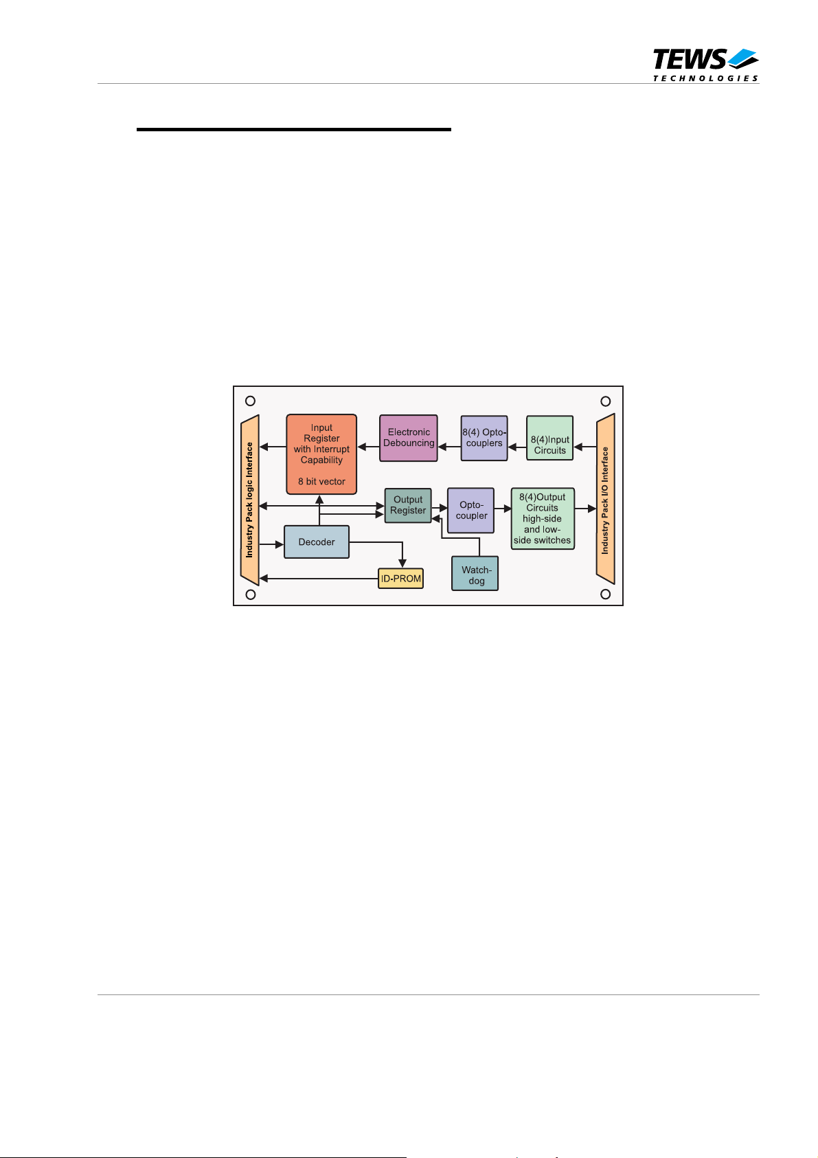
1 Product Description
The TIP670 is an IndustryPack compatible module with 8 (4) digital inputs galvanically isolated by
optocoupler. The individual inputs are potential free in relation to each other. A high performance input
circuit ensures a defined switching point and polarization protection against confusing the pol e.
All inputs have an electronic debounce circuit with fixed debounce time. All inputs can generate an
interrupt. The signal edge handling is programmable. For systems with particularly fast reaction, each
input can be assigned its own interrupt vector.
The TIP670 has 8 (4) digital outputs with galvanic isolation via optocouplers. The outputs are isolated
against each other in groups of two. All outputs resist short-circuits and are protected against thermal
overload.
The output drivers are capable of driving 0.5A continuous per channel. Each output can be configured
individually as high or low side switch.
Figure 1-1 : Block Diagram
TIP670 User Manual Issue 1.3 Page 5 of 19
Page 6
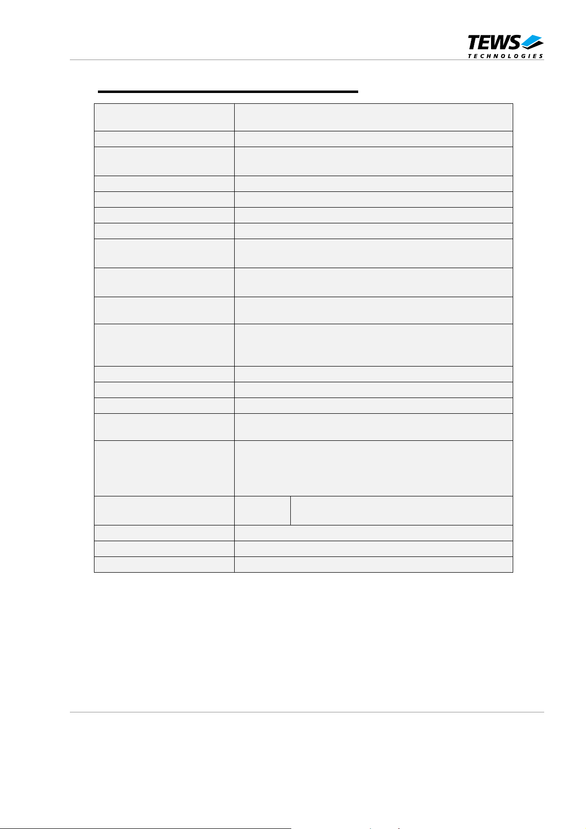
2 Technical Specification
Logic Interface
Interface Connector
Number of Inputs
Input Isolation
Input Voltage
Input Current
Input Switching Level
Wait States
Number of Digital Outputs
Output Isolation
External Supply Voltage for
Outputs
Output Current
Short Circuit Current
Output Voltage Drop
Output Protection
Power Requirements
Temperature Range
MTBF
Humidity
Transition Module
Single Size IndustryPack Logic Interface compliant to
ANSI/VITA 4-1995
50-conductor flat cable
TIP670-10: 8
TIP670-20: 4
All channels are completely independent from each other
24V DC
4.2mA typical @+24V input voltage
12V typical (minimum 9V, maximum 13V)
ID PROM: 0 wait states
I/O (Z8536 CIO): minimum 3 wait states
TIP670-10: 8
TIP670-20: 4
All channels, each two channels shares the same power
supply and ground
24V DC typical
6V DC minimum
48V DC maximum
0.5A (0.4A for voltages over 32V)
0.8A typical (2A maximum)
1.1V typical @+0.5A
Overload, short circuit, GND and Vs open wire protection,
thermal shutdown
TIP670-10:
280mA typical @+5V DC (all inputs and outputs active)
TIP670-20:
250mA typical @+5V DC (all inputs and outputs active)
Operating
Storage
920276 h
5 – 95 % non-condensing
Optional (TIP001-TM-10)
0 °C to +70 °C
-45°C to +125°C
Figure 2-1 : Technical Specification
TIP670 User Manual Issue 1.3 Page 6 of 19
Page 7
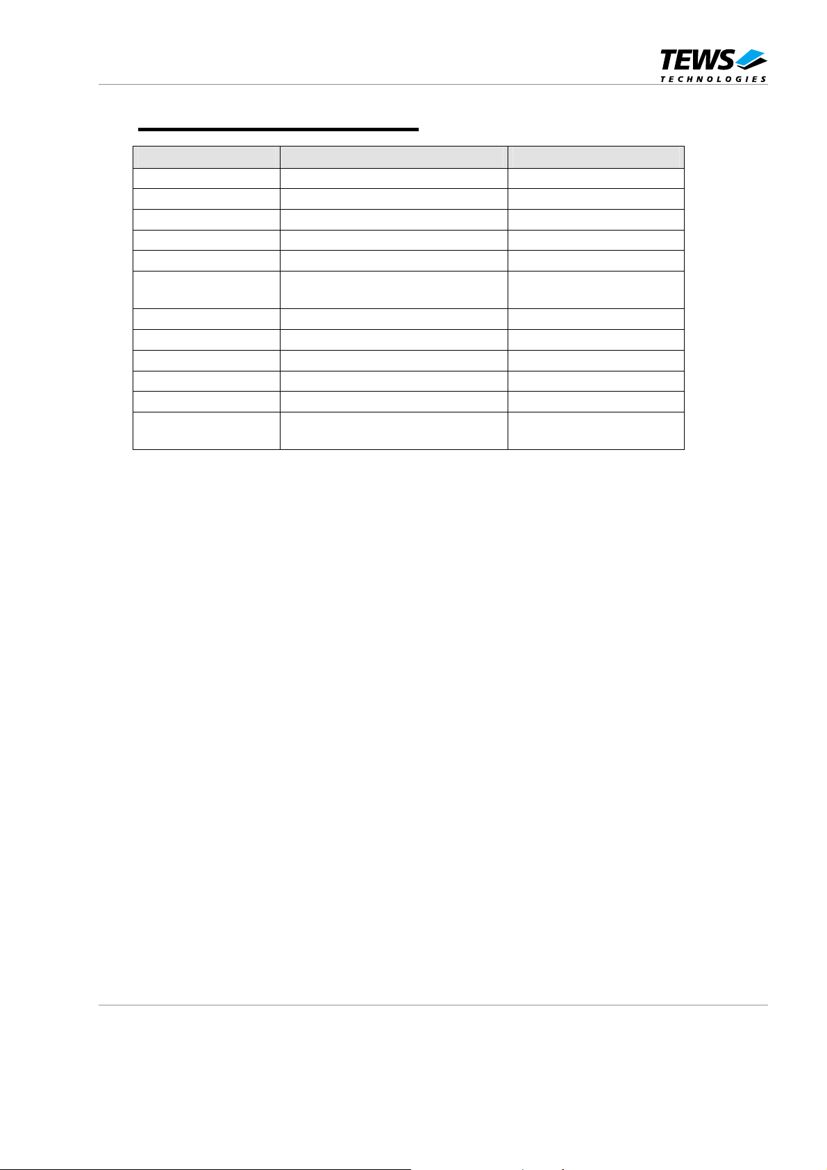
3 ID Prom Contents
Address Function Contents
0x01
0x03
0x05
0x07
0x09
0x0B
0x0D
0x0F
0x11
0x13
0x15
0x17
ASCII ‘I’
ASCII ‘P’
ASCII ‘A’
ASCII ‘C’
Manufacturer ID
Model Number
Revision
Reserved
Driver-ID low byte
Driver-ID high byte
Number of bytes used
CRC
Figure 3-1 : ID PROM Contents
0x49
0x50
0x41
0x43
0xB3
0x02 (for TIP670-10)
0x03 (for TIP670-20)
0x10
0x00
0x00
0x00
0x0C
0x93 (for TIP670-10)
0xF2 (for TIP670-20)
TIP670 User Manual Issue 1.3 Page 7 of 19
Page 8
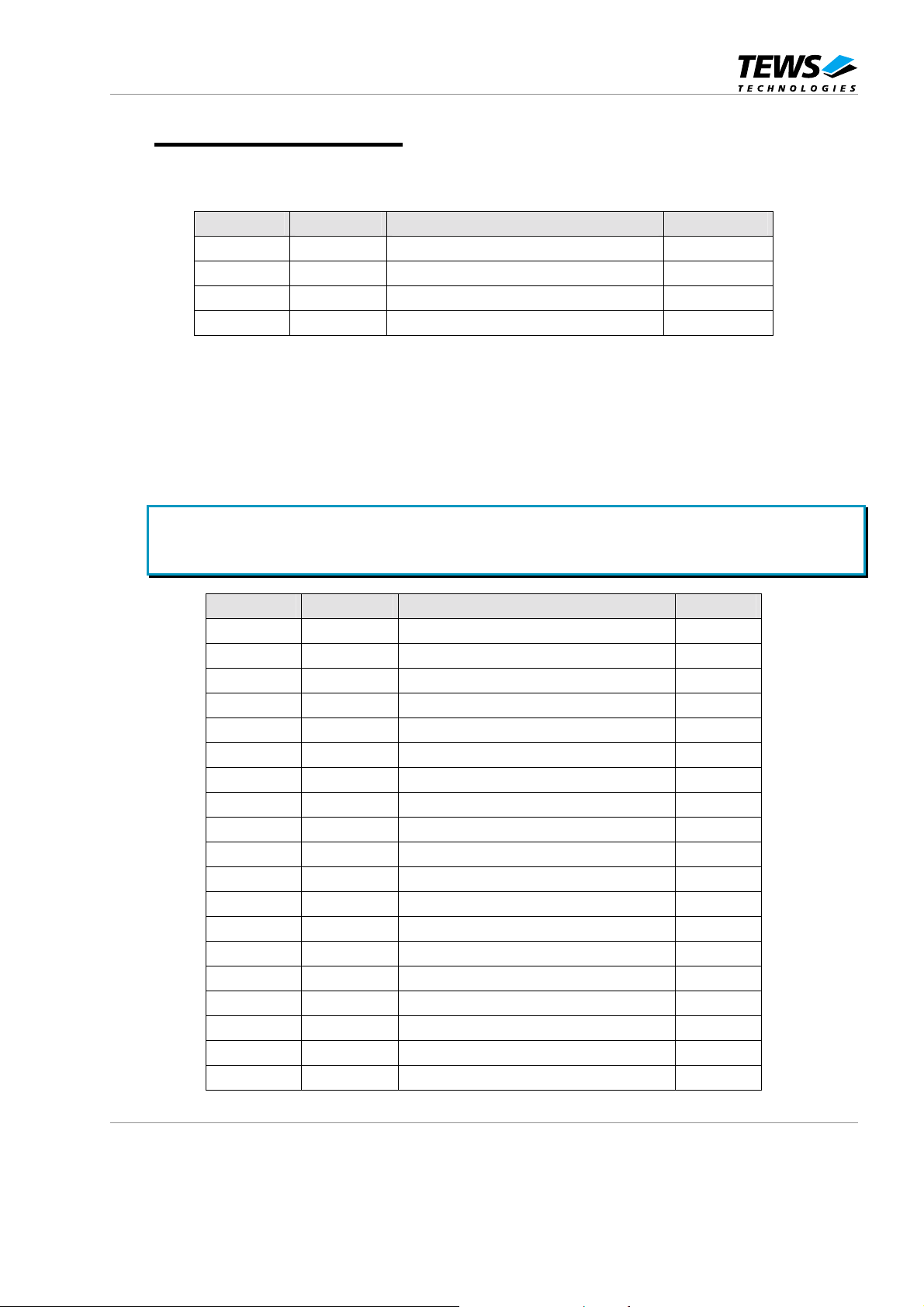
4 IP Addressing
The TIP670 is accessed in the I/O space through the following set of four direct accessible registers
implemented in the Z8536 controller:
Address Symbol Description Size (Bit)
0x01 PORTC Port C Data Bits D00-D07 8
0x03 PORTB Port B Data Bits D00-D07 8
0x05 PORTA Port A Data Bits D00-D07 8
0x07 CIOCSR CIO Command and Status Register 8
Figure 4-1 : Register Set
4.1 Indirect Addressable Registers
In addition to the above mentioned direct access registers the Z8536 CIO has 48 indirect
addressable registers. These indirect addressable registers are used for the mode specification
and for the control of ports and counter/timers.
Not all of the indirect addressable registers are required for the operation of the TIP670. For a
more detailed description of the function of these registers see the Z8536 data sheet which is
part of the Engineering Documentation TIP670-ED.
Address Symbol Description Size (Bit)
0x00 MICR Master Interrupt Control 8
0x01 MCCR Master Configuration Control 8
0x02 PAIV Port A Interrupt Vector 8
0x03 PBIV Port B Interrupt Vector 8
0x04 CTIV Counter / Timer Interrupt Vector 8
0x05 PCDP Port C Data Path Polarity 8
0x06 PCDD Port C Data Direction 8
0x07 PCSC Port C Special I/O Control 8
0x08 PACS Port A Control / Status 8
0x09 PBCS Port B Control / Status 8
0x0A C1CSR Counter / Timer 1 Command / Status 8
0x0B C2CSR Counter / Timer 2 Command / Status 8
0x0C C3CSR Counter / Timer 3 Command / Status 8
0x0D PADR Port A Data Register 8
0x0E PBDR Port B Data Register 8
0x0F PCDR Port C Data Register 8
0x10 CT1CM Counter / Timer 1 Current Count MSB 8
0x11 CT1CL Counter / Timer 1 Current Count LSB 8
0x12 CT2CM Counter / Timer 2 Current Count MSB 8
TIP670 User Manual Issue 1.3 Page 8 of 19
Page 9

0x13 CT2CL Counter / Timer 2 Current Count LSB 8
0x14 CT3CM Counter / Timer 3 Current Count MSB 8
0x15 CT3CL Counter / Timer 3 Current Count LSB 8
0x16 CT1PM Counter / Timer 1 Preload MSB 8
0x17 CT1PL Counter / Timer 1 Preload LSB 8
0x18 CT2PM Counter / Timer 2 Preload MSB 8
0x19 CT2PL Counter / Timer 2 Preload LSB 8
0x1A CT3PM Counter / Timer 3 Preload MSB 8
0x1B CT3PL Counter / Timer 3 Prelo ad LSB 8
0x1C CT1MO Counter / Timer 1 Mode Specification 8
0x1D CT2MO Counter / Timer 2 Mode Specification 8
0x1E CT3MO Counter / Timer 3 Mode Specification 8
0x1F CTCV Counter / Timer Current Vector 8
0x20 PAMO Port A Mode Specification 8
0x21 PAHS Port A Handshake Specification 8
0x22 PADP Port A Data Path Polarity 8
0x23 PADD Port A Data Direction 8
0x24 PASC Port A Special I/O Control 8
0x25 PAPP Port A Pattern Polarity 8
0x26 PAPT Port A Pattern Transition 8
0x27 PAPM Port A Pattern Mask 8
0x28 PBMO Port B Mode Specification 8
0x29 PBHS Port B Handshake Specification 8
0x2A PBDP Port B Data Path Polarity 8
0x2B PBDD Port B Data Direction 8
0x2C PBSC Port B Special I/O Control 8
0x2D PBPP Port B Pattern Polarity 8
0x2E PBPT Port B Pattern Transition 8
0x2F PBPM Port B Pattern Mask 8
Figure 4-2 : Z8536 CIO Indirect Addressable Registers
TIP670 User Manual Issue 1.3 Page 9 of 19
Page 10
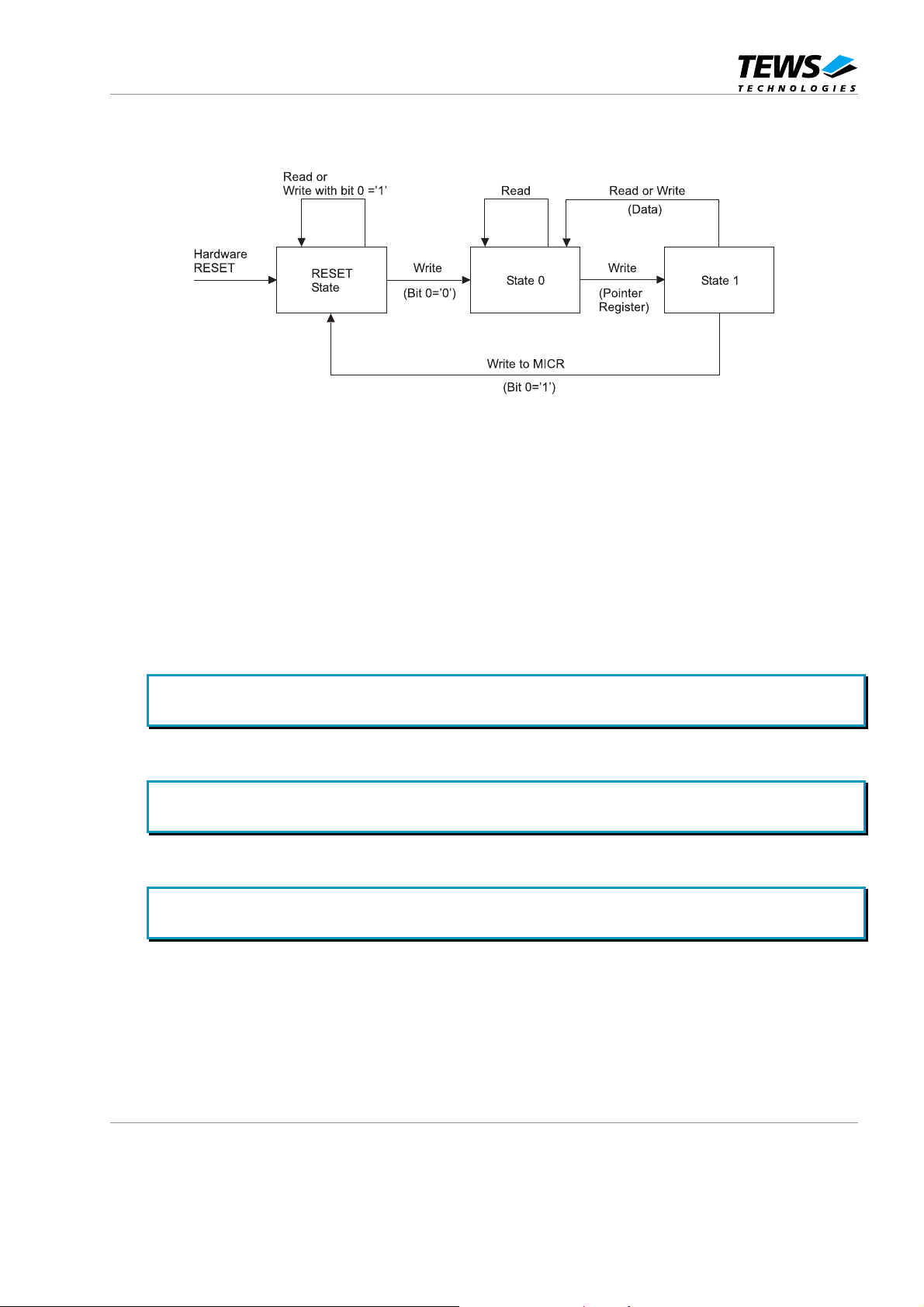
The access to the indirect addressable register is controlled by a state machine and a hidden pointer
register. The state machine takes 3 different states: RESET state, state ” 0 ” or state ” 1 ”.
Figure 4-3 : CIO State Machine
A hardware reset will put the state machine into RESET state. In RESET state it is only possible to
read or write the RESET bit (bit 0) in the Master Interrupt Control Register (MICR). A write access with
the RESET bit (bit 0) = 0 will put the state machine into state ” 0 ”.
Writing in state ” 0 ” loads the internal pointer register with the internal register address to select the
chosen register. This will put also the state machine into state ” 1 ”.
A read or write access in state ” 1 ” will transfer data from or to the internal register which was selected
by the pointer register. Any access to the internal registers puts the state machine back into state ” 0 ”.
Any read in state ” 0 ” returns the contents of the last register pointed to. Therefore, a register can be
read continuously without again writing to the pointer.
Outside the RESET state any read will put the state machine into state ‘0’. So a dummy read
can be used to bring the state machine in this known state.
If the state machine is in state ‘1’, some of the internal operation of the CIO is disabled. So the
state machine should never be left in state ‘1’ longer as necessary.
Direct accesses to the data register PORTA, PORTB, and PORTC have no consequence for the
status of the state machine.
TIP670 User Manual Issue 1.3 Page 10 of 19
Page 11

5 Functional Description
5.1 Digital Inputs
5.1.1 Optical Isolation
The TIP670 has 8 (TIP670-10) or 4 (TIP670-20) digital inputs. The standard signal level for these
inputs is 24V DC. The switching level of the inputs is between 8 and 13 volts. All input channels are
isolated by AC optocoupler and are also isolated against each other. The use of AC optocoupler
makes the operation of the inputs independent from signal polarity.
5.1.2 Digital Filtering
A digital filter circuit is provided for input switch debouncing. The debounce time is adjusted by a
capacitor to approximately 12ms.
5.1.3 Input and Interrupt Logic
The input and interrupt logic is implemented in the Z8536 port controller circuit. The digitally filtered
input signals are connected with port B of the Z8536.
Interrupt generation can be individually programmed for each channel and input transition. For more
detailed information see the Z8536 data manual which is part of the TIP670-ED Engineering
Documentation.
A software initialization of the Z8536 is required before the input states can be read at port B.
5.2 Digital Outputs
5.2.1 Optical Isolation
The TIP670 has 8 (TIP670-10) or 4 (TIP670-20) digital outputs. The standard signal level for these
outputs is 24V DC. All output channels are isolated by optocoupler and are also isolated against each
other in groups of two outputs.
5.2.2 Output Polarity
Each output can be individually configured as a high or a low side switch depending on the external
wiring of the output signal lines.
5.2.3 Overload Protection
The output drivers are implemented by smart drivers TDExxx. The maximum continuous output
current is 0.5A. The output circuits are protected against overload, short circuit and thermal overload.
In case of such a failure the corresponding output will be disabled until the error condition is removed.
Then the output returns automatically to normal operation.
TIP670 User Manual Issue 1.3 Page 11 of 19
Page 12

5.2.4 Output Watchdog
Counter/Timer 3 and Port C of the Z8536 can be programmed to implement a watchdog for the
outputs. Any software access to the Z8536 will retrigger Timer 3 in the Z8536. If the programmed time
expires without a software access all outputs go into the ’off’ state (the maximum programmable time
is approx. 30ms). However they will return to their original state, when the TIP670 is accessed again
by the software.
The watchdog is disabled after power-up or reset.
TIP670 User Manual Issue 1.3 Page 12 of 19
Page 13

6 Programming
After power-up or system reset the CIO Z8536 is in its initial state and the I/O ports A, B, C are
disabled and configured to output direction. For normal operation of the TIP670 a minimum software
initialization is required.
6.1 Required Software Initialization
The input lines of the TIP670 are connected to port B of the CIO Z8536. This port has to be configured
as input and because of the inverting function of the optocouplers the input polarity has to be set to
inverting.
To perform this required software initialization sees the following procedure:
• Write 0x00 to CIOSR
Write 0x01 to CIOSR
Write 0x00 to CIOSR
This sequence puts the CIO Z8536 into a known (reset) state
• Write 0x2B to CIOCSR
This selects the Port B Data Direction Register (PBDD) for the next operation
• Write 0xFF to CIOCSR
Writing 0xFF into PBDD will configure all bits of port B as input
• Write 0x2A to CIOCSR
This selects the Port B Data Path Polarity Register (PBDP) for the next operation
• Write 0xFF to CIOCSR
Writing 0xFF into PBDP will configure all bits of port B to be inverted
• Write 0x01 to CIOCSR
This selects the Master Configuration Control Register (MCCR) for the next operation
• Write 0x84 to CIOCSR
Writing 0x84 into MCCR will enable port A and B
After this sequence the directly accessible port registers Port A and Port B can be used for reading the
actual status of the TIP670 input and setting the TIP670 outputs.
TIP670 User Manual Issue 1.3 Page 13 of 19
Page 14

6.2 Initialization of the Watchdog Function
On the TIP670 port C and counter timer 3 of the Z8536 are wired in way, that a watchdog function can
be programmed into the TIP670. This watchdog is retriggered with every access to the TIP670. If
there is no access within a previously programmed time frame, the watchdog will automatically disable
the output lines.
If the TIP670 is accessed after the watchdog timer has expired, the output lines will return to its
original state.
For initialization of the watchdog function proceed as follow:
• Write 0x1E to CIOCSR
This selects the Counter/Timer 3 Mode Specification Register (CT3MO) fo r the next operation
• Write 0x55 to CIOCSR
Writing 0x55 into CT3MO will configure counter/timer 3 to single cycle, retrigger enable, external
output, one shot
• Write 0x1A to CIOCSR
This selects the Counter/Timer3 Preload MSB Register (CT3PM) for the next operation
• Write 0xF0 to CIOCSR
Writing 0xF0 into CT3PM will load the first half of the watchdog time out time of ‘0xF000’ which is
just an example for approx. 30ms
• Write 0x1B to CIOCSR
This selects the Counter/Timer3 Preload LSB Register (CT3PL) for the next operation
• Write 0x00 to CIOCSR
Writing 0x00 into CT3PL will load the second half of the watchdog time out time of ‘0xF000’ which
is just an example for approx. 30ms
• Write 0x06 to CIOCSR
This selects the Port C Data Direction Register (PCDD) for the next operation
• Write 0x04 to CIOCSR
Writing 0x04 into PCDD configures bit 2 as an input for retrigger
• Write 0x01 to CIOCSR
This selects the Master Configuration Control Register (MCCR) for the next operation
• Write 0x84 to CIOCSR
Writing 0x84 into MCCR will enable port A and B
• Write 0x0F to CIOCSR
This selects the Port C Data Register (PCDR) for the next operation
• Write 0x70 to CIOCSR
Writing 0x70 into PCDR configures bit 3 as an writable output
TIP670 User Manual Issue 1.3 Page 14 of 19
Page 15

• Write 0x0C to CIOCSR
This selects the Counter/Timer 3 Command and Status Register (C3CSR) for the next operation
• Write 0x06 to CIOCSR
Writing 0x06 into C3CSR triggers and runs counter timer 3
• Write 0x00 to PORTC
Writing 0x00 to PORTC will enable the watchdog function
TIP670 User Manual Issue 1.3 Page 15 of 19
Page 16
7 Installation
7.1 Input Wiring
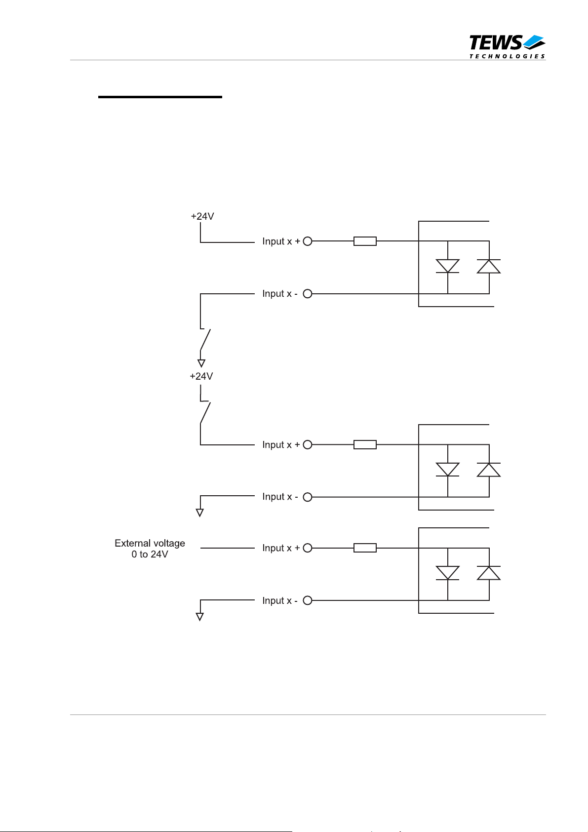
Each input is optically isolated from the logic circuit. Each input is independent of the other inputs and
can be wired different. Each input has two connections at the IP I/O connector, Input x + and Input x -.
However the TIP670 has AC optocoupler at the input side. Therefore the polarity of the input signal
may be either way.
Figure 7-1 : Input Wiring Options
TIP670 User Manual Issue 1.3 Page 16 of 19
Page 17
7.2 Output Wiring
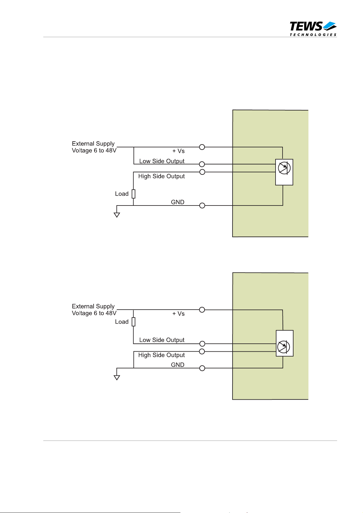
The outputs are optically isolated from the logic circuit in groups of two. Output channels 1 and 2, 3
and 4, 5 and 6, 7 and 8 share the same output potential but are completely isolated against the other
output pairs.
Each output can be individually configured as a high side or a low side switch by correspondi ng wiring.
Figure 7-2 : Output Wiring as High Side Switch
Figure 7-3 : Output Wiring as Low Side Switch
TIP670 User Manual Issue 1.3 Page 17 of 19
Page 18
8 Pin Assignment – I/O Connector
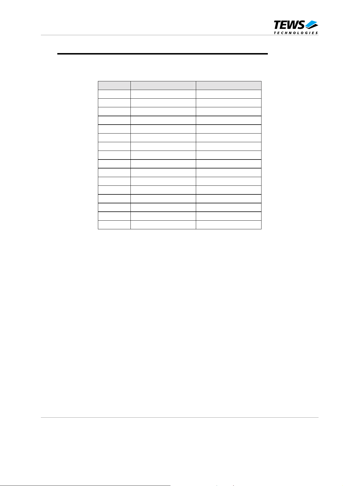
8.1 Input Connections
Pin Signal Comment
01 Input 1+
02 Input 1-
03 Input 2+
04 Input 2-
05 Input 3+
06 Input 3-
07 Input 4+
08 Input 4-
09 Input 5+ TIP670-10 only
10 Input 5- TIP670-10 only
11 Input 6+ TIP670-10 only
12 Input 6- TIP670-10 only
13 Input 7+ TIP670-10 only
14 Input 7- TIP670-10 only
15 Input 8+ TIP670-10 only
16 Input 8- TIP670-10 only
Figure 8-1 : Input I/O connection
TIP670 User Manual Issue 1.3 Page 18 of 19
Page 19
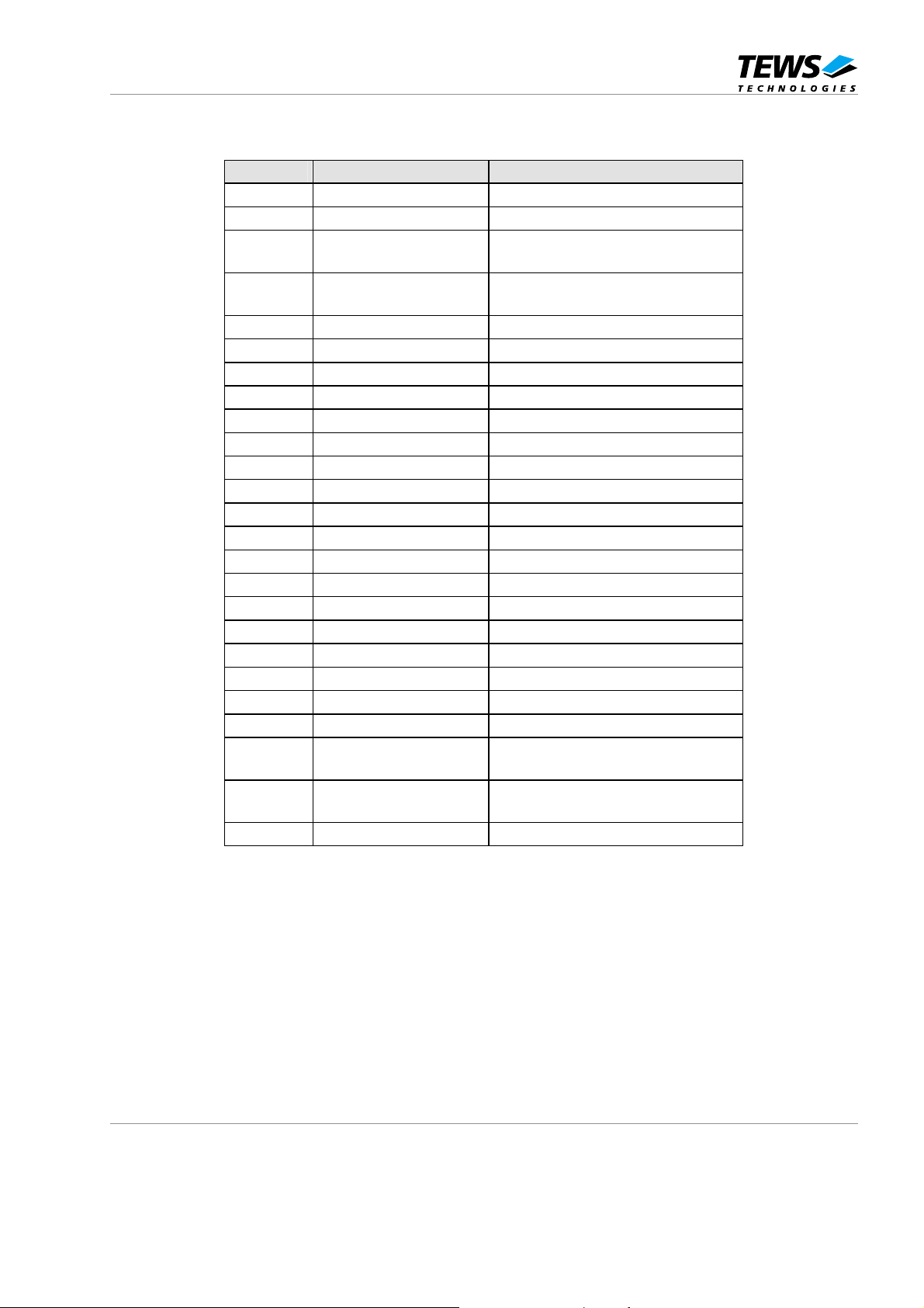
8.2 Output Connections
Pin Signal Comment
26 GND 1-2 External GND for Output 1-2
27 GND 3-4 External GND for Output 3-4
28 GND 5-6 External GND for Output 5-6
29 GND 7-8 External GND for Output 7-8
30 Low Side Output 1
31 High Side Output 1
32 Low Side Output 2
33 High Side Output 2
34 Low Side Output 3
35 High Side Output 3
36 Low Side Output 4
37 High Side Output 4
38 Low Side Output 5 TIP670-10 only
39 High Side Output 5 TIP670-10 only
40 Low Side Output 6 TIP670-10 only
41 High Side Output 6 TIP670-10 only
42 Low Side Output 7 TIP670-10 only
43 High Side Output 7 TIP670-10 only
44 Low Side Output 8 TIP670-10 only
45 High Side Output 8 TIP670-10 only
46 +Vs 1-2 External Supply Voltage for Output 1-2
47 +Vs 3-4 External Supply Voltage for Output 3-4
48 +Vs 5-6 External Supply Voltage for Output 5-6
49 +Vs 7-8 External Supply Voltage for Output 7-8
50 NC
(TIP670-10 only)
(TIP670-10 only)
(TIP670-10 only)
(TIP670-10 only)
Figure 8-2 : Output I/O connection
TIP670 User Manual Issue 1.3 Page 19 of 19
 Loading...