

Page 1

The Embedded I/O Company
TIP606
Digital Input Module for
Avionic Applications
Version 1.0
User Manual
Issue 1.3
September 2006
D75606800
TEWS TECHNOLOGIES GmbH TEWS TECHNOLOGIES LLC
Am Bahnhof 7
25469 Halstenbek, Germany
www.tews.com
Phone: +49-(0)4101-4058-0
Fax: +49-(0)4101-4058-19
e-mail: [email protected]
9190 Double Diamond Parkway,
Suite 127, Reno, NV 89521, USA
www.tews.com
Phone: +1 (775) 850 5830
Fax: +1 (775) 201 0347
e-mail: [email protected]
Page 2

TIP606 User Manual Issue 1.3 Page 2 of 15
TIP606-10
Digital Input Module for Avionic Applications
This document contains information, which is
proprietary to TEWS TECHNOLOGIES GmbH. Any
reproduction without written permission is forbidden.
TEWS TECHNOLOGIES GmbH has made any
effort to ensure that this manual is accurate and
complete. However TEWS TECHNOLOGIES GmbH
reserves the right to change the product described
in this document at any time without notice.
TEWS TECHNOLOGIES GmbH is not liable for any
damage arising out of the application or use of the
device described herein.
Style Conventions
Hexadecimal characters are specified with prefix 0x,
i.e. 0x029E (that means hexadecimal value 029E).
For signals on hardware products, an ‚Active Low’ is
represented by the signal name with # following, i.e.
IP_RESET#.
Access terms are described as:
W Write Only
R Read Only
R/W Read/Write
R/C Read/Clear
R/S Read/Set
2000-2006 by TEWS TECHNOLOGIES GmbH
IndustryPack is a registered trademark of SBS Technologies, Inc
Page 3

TIP606 User Manual Issue 1.3 Page 3 of 15
Issue Description Date
1.0 First Issue March 2000
1.1 General Revision October 2003
1.2
Correction of figure “
Input Circuit” in chapter “Functional
Description”
January 2006
1.3 New address TEWS LLC September 2006
Page 4

TIP606 User Manual Issue 1.3 Page 4 of 15
Table of Contents
1 PRODUCT DESCRIPTION.........................................................................................6
2 TECHNICAL SPECIFICATION...................................................................................7
3 ID PROM CONTENTS................................................................................................ 8
4 IP ADDRESSING........................................................................................................9
4.1 I/O Addressing.................................................................................................................................9
4.2 Input Register (INPUT)....................................................................................................................9
4.3 Global Control Register (GLBCONT) ..........................................................................................10
4.4 Interrupt Enable Register Rising Edge (INTENALH) .................................................................10
4.5 Interrupt Enable Register Falling Edge (INTENAHL).................................................................11
4.6 Interrupt Status Register Rising Edge (INTSTATLH) ................................................................11
4.7 Interrupt Status Register Falling Edge (INTSTATHL)................................................................11
4.8 Interrupt Vector Register (IVEC)..................................................................................................12
4.9 Debounce Time Register (DEBTIME) ..........................................................................................12
5 FUNCTIONAL DESCRIPTION .................................................................................13
6 PIN ASSIGNMENT – I/O CONNECTOR ..................................................................15
Page 5

TIP606 User Manual Issue 1.3 Page 5 of 15
Table of Figures
FIGURE 1-1 : BLOCK DIAGRAM......................................................................................................................6
FIGURE 2-1 : TECHNICAL SPECIFICATION...................................................................................................7
FIGURE 3-1 : ID PROM CONTENTS ...............................................................................................................8
FIGURE 4-1 : REGISTER SET .........................................................................................................................9
FIGURE 4-2 : INPUT REGISTER (INPUT).......................................................................................................9
FIGURE 4-3 : GLOBAL CONTROL REGISTER (GLBCONT)........................................................................10
FIGURE 4-4 : INTERRUPT ENABLE REGISTER RISING EDGE (INTENALH)............................................10
FIGURE 4-5 : INTERRUPT ENABLE REGISTER FALLING EDGE (INTENAHL)..........................................11
FIGURE 4-6 : INTERRUPT STATUS REGISTER RISING EDGE (INTSTATLH) ..........................................11
FIGURE 4-7 : INTERRUPT STATUS REGISTER FALLING EDGE (INTSTATHL)........................................11
FIGURE 4-8 : INTERRUPT VECTOR REGISTER (IVEC)..............................................................................12
FIGURE 4-9 : DEBOUNCE TIME REGISTER (DEBTIME).............................................................................12
FIGURE 5-1 : INPUT CIRCUIT.......................................................................................................................13
FIGURE 5-2 : HIGH SIDE AND LOW SIDE SWITCHING..............................................................................14
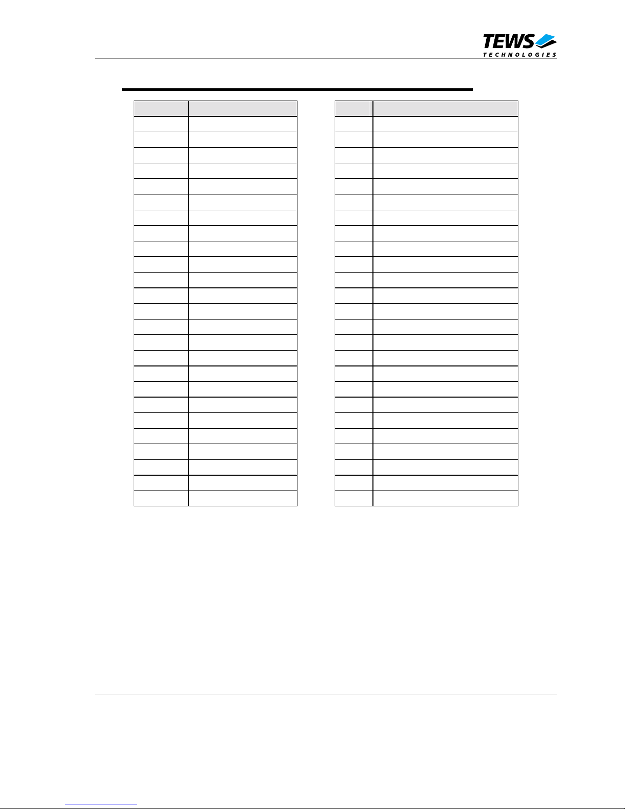
FIGURE 6-1 : PIN ASSIGNMENT I/O CONNECTOR.....................................................................................15
Page 6
TIP606 User Manual Issue 1.3 Page 6 of 15
1 Product Description
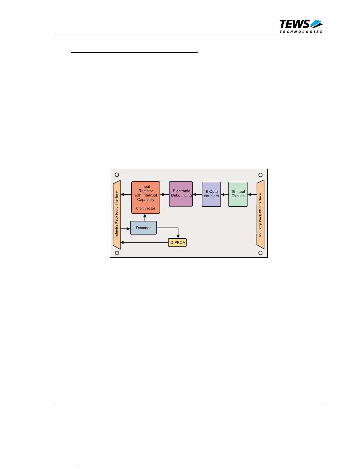
The TIP606 is an IndustryPack® compatible module designed for avionic test environments. It
provides 16 optically isolated differential inputs for high unipolar input voltage which may exceed the
supply voltage of the module. The inputs can withstand input voltage up to 44V maximum between the
two differential input pins.
Due to the differential inputs of the TIP606, it is even possible to use the module in noisy
environments. The TIP606 provides a high differential input resistance of 112 kohms typically.
The interface circuit will detect a logic 1, if the differential voltage is typically greater than +14.0V and it
will detect a logic 0, if the input voltage is typically lower than +3.5V. The inputs are isolated from the
IP interface via optocouplers. Each input is capable of generating interrupts on rising or falling edges
of the input signal. It is also possible to disable the generation of interrupts and poll the input register
for new data.
All inputs have an electronic debounce circuit. The debounce time is programmable in a range from
900µs up to 230ms in 256 steps of 900µs. The debounce circuit can also be disabled.
Figure 1-1 : Block Diagram
Page 7

TIP606 User Manual Issue 1.3 Page 7 of 15
2 Technical Specification
IP Interface
Interface
Single Size IndustryPack Logic Interface compliant to
ANSI/VITA 4-1995
ID ROM Data
Format I
Interrupts
INTREQ0# used
DMA
Not supported
Clock Rate
8 MHz
Module Type
Type I
Wait States
No wait states
Interrupts
Interrupt generation for each input
programmable on Low -> high transition, High -> low transition
Number of Inputs
16 differential
Maximum Input Voltage
44V between U_in+ and U_in-
Input Isolation Voltage
500Vpp
Input Switching Level
High level: >14.0V typical @+25°C (13.0V-16.0V)
Low level: <3.5V typical @ +25°C (3.1V-4.6V)
Input Impedance
112 kohms typical
Debounce Timer
Time minimum: 900µs +/-15%
Time maximum: 230.4ms +/-15%
Step size: 900µs
Interface Connector
50-conductor flat cable
Power Requirements
150mA typical @ +5V DC
Physical Data
Temperature Range
Operating
Storage
-40 °C to +85 °C
-55°C to +125°C
MTBF
124109 h
Humidity
5 – 95 % non-condensing
Weight
28 g
Figure 2-1 : Technical Specification
Page 8
TIP606 User Manual Issue 1.3 Page 8 of 15
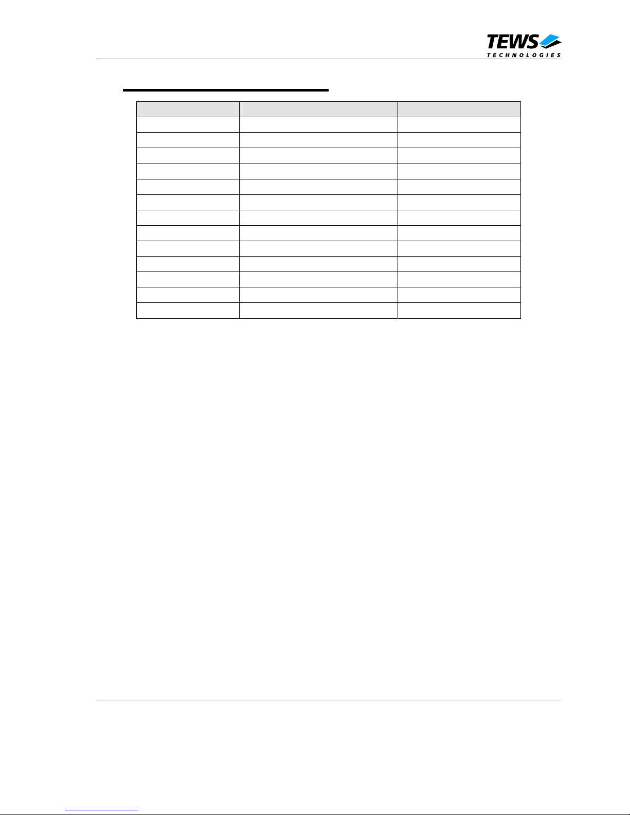
3 ID PROM Contents
Address Function Contents
0x01
ASCII ‘I’
0x49
0x03
ASCII ‘P’
0x50
0x05
ASCII ‘A’
0x41
0x07
ASCII ‘C’
0x43
0x09
Manufacturer ID
0xB3
0x0B
Model Number
0x2E
0x0D
Revision
0x10
0x0F
Reserved
0x00
0x11
Driver-ID Low - Byte
0x00
0x13
Driver-ID High - Byte
0x00
0x15
Number of bytes used
0x0C
0x17
CRC
0x0E
0x19
Version
0x0A
Figure 3-1 : ID PROM Contents
Page 9
TIP606 User Manual Issue 1.3 Page 9 of 15
4 IP Addressing
4.1 I/O Addressing
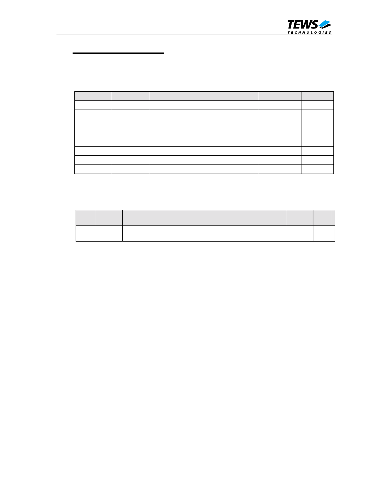
The complete register set of the TIP606 is accessible in the I/O space of the IP.
Address Symbol Description Size (Bit) Access
0x00 INPUT Input Register 16 R
0x03 GLBCONT Global Control Register 8 R/W
0x04 INTENALH Interrupt Enable Register Rising Edge 16 R/W
0x06 INTENAHL Interrupt Enable Register Falling Edge 16 R/W
0x08 INTSTATLH Interrupt Status Register Rising Edge 16 R/W
0x0A INSTATHL Interrupt Status Register Falling Edge 16 R/W
0x0D IVEC Interrupt Vector Register 8 R/W
0x0F DEBTIME Debounce Time Register 8 R/W
Figure 4-1 : Register Set
4.2 Input Register (INPUT)
Bit Symbol Description Access
Reset
Value
15:0
16 bit input data. Register reflects the actual state of the
inputs.
R
Figure 4-2 : Input Register (INPUT)
Page 10
TIP606 User Manual Issue 1.3 Page 10 of 15
4.3 Global Control Register (GLBCONT)
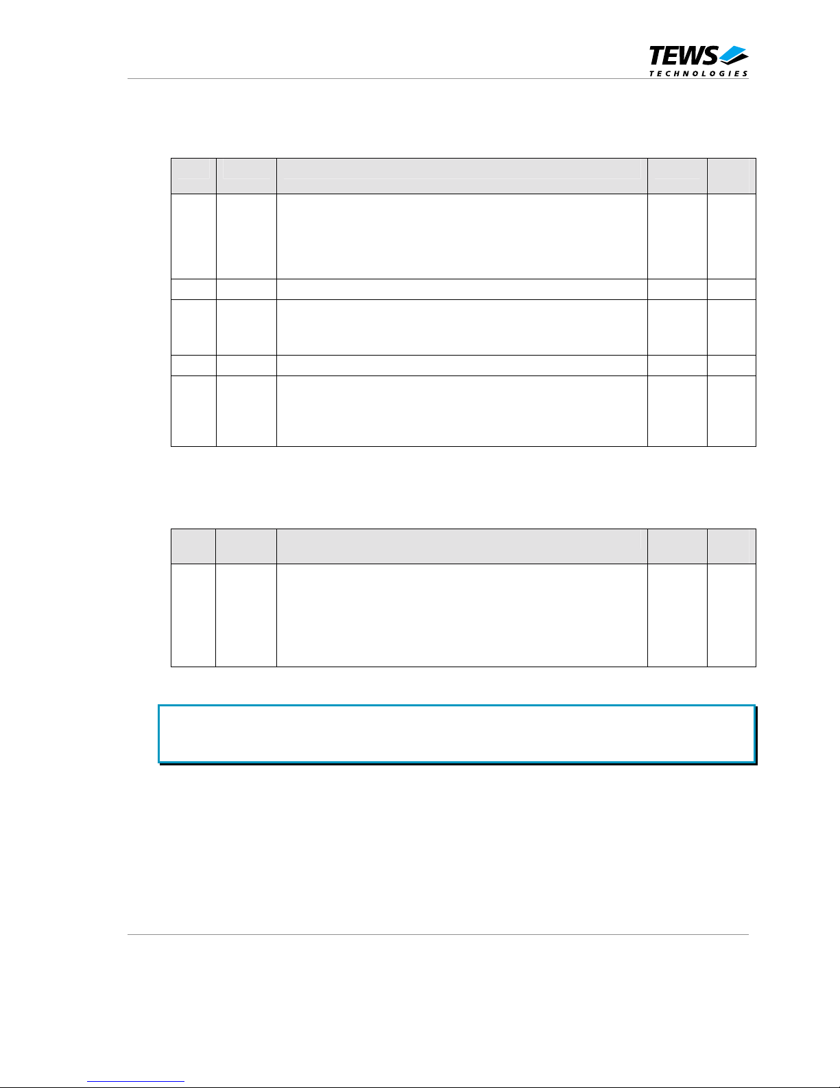
After power up or reset all bits of this register are reset to ‘0’.
Bit Symbol Description Access
Reset
Value
7 Global interrupt flag
1 = an interrupt request of at least one of the 16 input
channels is pending.
Bit will be cleared if the appropriate interrupt is acknowledged
by writing ‘1’ to one of the interrupt status registers.
R
6:3 Not used, undefined during reads R/W
2 Debounce control bit
1 = enables debounce circuit for all 16 inputs
0 = disables debounce circuit
R/W
1 Not used, undefined during reads R/W
0 Global interrupt enable bit
1 = enables all possible interrupts of the TIP606 on interrupt
request line INTREQ0# of the IP bus
0 = disables all interrupts
R/W
Figure 4-3 : Global Control Register (GLBCONT)
4.4 Interrupt Enable Register Rising Edge (INTENALH)
Bit Symbol Description Access
Reset
Value
15
.
.
.
0
Interrupt enable bit of corresponding channel for the rising
edge
Bit 0 enables interrupts of input channel 1 and bit 15 enables
interrupt of input channel 15 rising edge.
1 = interrupt enabled
0 = interrupt disabled
R/W
Figure 4-4 : Interrupt Enable Register Rising Edge (INTENALH)
An interrupt on interrupt request line INTREQ0# of the IP bus is only generated if the global
interrupt enable bit of the Global Control Register is set to ‘1’. After power up or reset all bits of
this register are reset to ‘0’.
Page 11
TIP606 User Manual Issue 1.3 Page 11 of 15
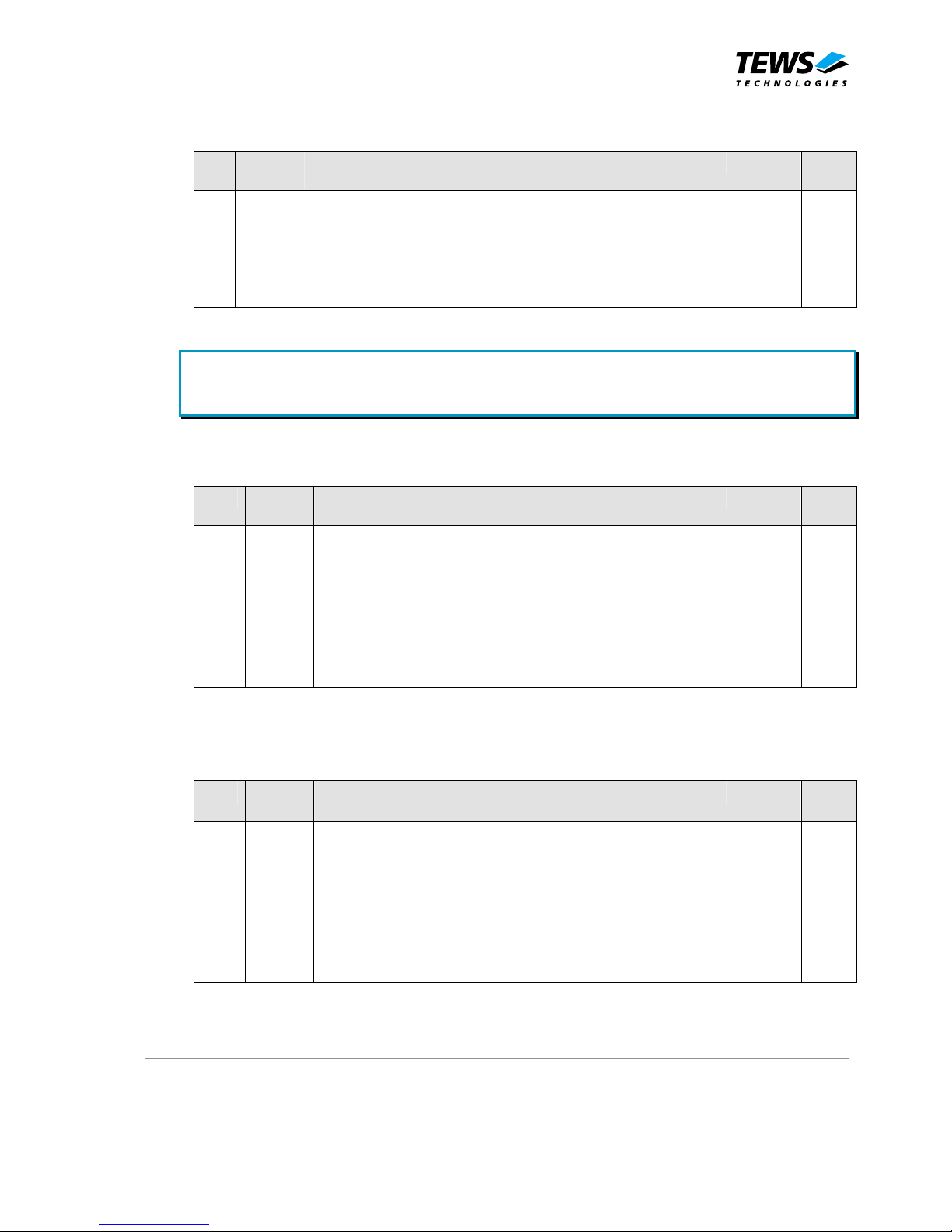
4.5 Interrupt Enable Register Falling Edge (INTENAHL)
Bit Symbol Description Access
Reset
Value
15
.
.
.
0
Interrupt enable bit of corresponding channel for the falling
edge.
Bit 0 enables interrupts of input channel 1 and bit 15 enables
interrupt of input channel 15 for the falling edge.
1 = interrupt enabled
0 = interrupt disabled
R/W
Figure 4-5 : Interrupt Enable Register Falling Edge (INTENAHL)
An interrupt on interrupt request line INTREQ0# of the IP bus is only generated if the global
interrupt enable bit of the Global Control Register is set to ‘1’. After power up or reset all bits of
this register are reset to ‘0’.
4.6 Interrupt Status Register Rising Edge (INTSTATLH)
Bit Symbol Description Access
Reset
Value
15
.
.
.
.
.
.
0
Interrupt status bit of corresponding input for the rising edge.
Bit 0 reflects the interrupt request state of input 1 and bit 15
reflects the interrupt request state of input 16 for the rising
edge.
Read ‘0’: no interrupt request pending
Read ‘1’: interrupt request pending
Write ‘1’: clear pending interrupt
After power up or reset all bits of this register are reset to ‘0’.
R/W
Figure 4-6 : Interrupt Status Register Rising Edge (INTSTATLH)
4.7 Interrupt Status Register Falling Edge (INTSTATHL)
Bit Symbol Description Access
Reset
Value
15
.
.
.
.
.
.
0
Interrupt status bit of corresponding input for the falling edge.
Bit 0 reflects the interrupt request state of input 1 and bit 15
reflects the interrupt request state of input 16 for the falling
edge.
Read ‘0’: no interrupt request pending
Read ‘1’: interrupt request pending
Write ‘1’: clear pending interrupt
After power up or reset all bits of this register are reset to ‘0’.
R/W
Figure 4-7 : Interrupt Status Register Falling Edge (INTSTATHL)
Page 12
TIP606 User Manual Issue 1.3 Page 12 of 15
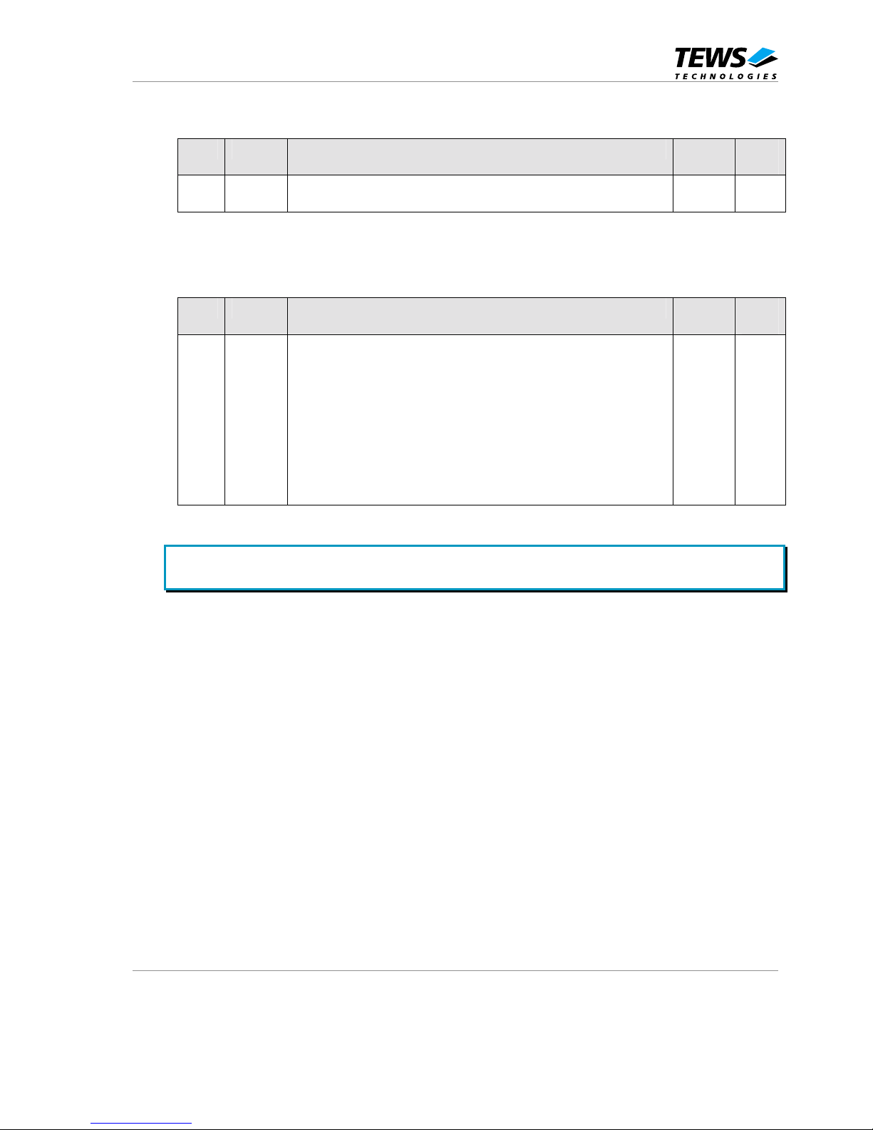
4.8 Interrupt Vector Register (IVEC)
Bit Symbol Description Access
Reset
Value
7:0
8 bit interrupt vector loaded by software. After power up or
reset all bits of this register are reset to ‘0’.
R/W
Figure 4-8 : Interrupt Vector Register (IVEC)
4.9 Debounce Time Register (DEBTIME)
Bit Symbol Description Access
Reset
Value
7:0 8 bit debounce preload value
The value 0 in this register sets the debounce time to a
minimum of 900µs (default after reset), if the debouncer is
enabled in the Global Control Register. A value of 255 sets
the debounce time to a maximum of 230.4ms. The debounce
time is common for all inputs.
The programmable debounce time can be calculated as
follows:
Debounce time = (x+1) * 900µs
x: 8 bit preload value in the range from 0 to 255.
R/W
Figure 4-9 : Debounce Time Register (DEBTIME)
The debounce time value can have a tolerance of up to +/-15% of the calculated value. The
debouncer will be enabled by writing ‘1’ to bit 2 of the Global Interrupt Control Register.
Page 13
TIP606 User Manual Issue 1.3 Page 13 of 15
5 Functional Description
U_in-
U_in+
R1
Differential Amp.
Schmitt-Trigger
+12V
V1
U_ref
V2
R2
R4
R5 R6
R3
R7 R9
R8 R10
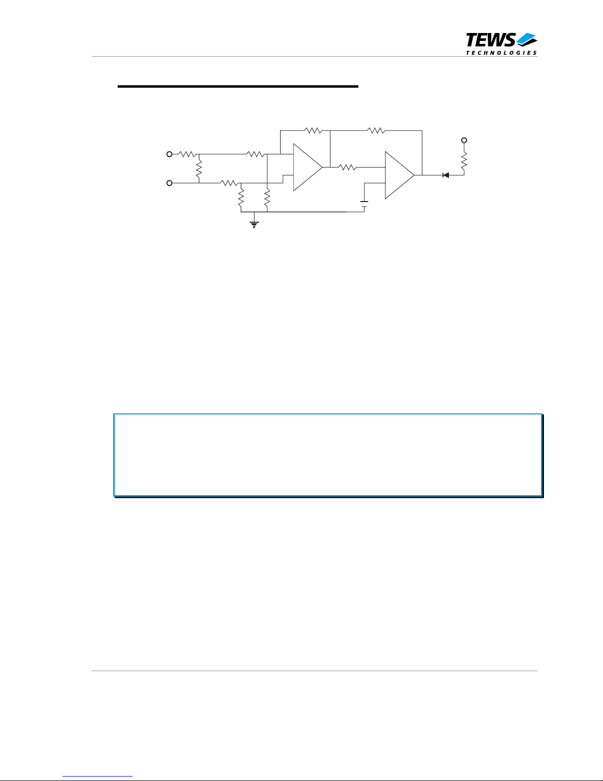
Figure 5-1 : Input Circuit
The input stage for each of the 16 inputs consists of a Differential Amplifier V1 followed by a SchmittTrigger V2. The Differential Amplifier provides a high impedance input for the input voltage. The input
impedance between U_in+ and U_in- is typically 112 kOhm. The Differential Amplifier amplifies only
the voltage difference across R2. The maximum frequency of the input signals should not exceed 10
kHz.
The thresholds of the TIP606 are determined by the resistor network around Opamp V2. At +25°C
ambient temperature the TIP606 will detect a high level typically at input voltages greater than 14.0V
and a low level at input voltages typically lower than 3.5V. These values can vary with the resistor
deviation (max +/-1%) and the operating temperature of the module (see product specification for
threshold bandwidth). The output voltage of each Schmitt-Trigger is fed to a separate optocoupler for
each input. The outputs of the optocouplers are connected to the inputs of a FPGA which are doing
the logic adaptation for the IP bus signaling.
To reduce power consumption of the TIP606 and avoid noise due to open inputs it is
recommended to connect unused U_in+ inputs to a signal level of 28V and U_in- inputs to the
respective ground signal.
The ground signal of the input signal source must be connected to the ground potential of the
input stage (pin 49 and 50 on IP connector P2) to guarantee the specified switching threshold
bandwidth.
Page 14
TIP606 User Manual Issue 1.3 Page 14 of 15
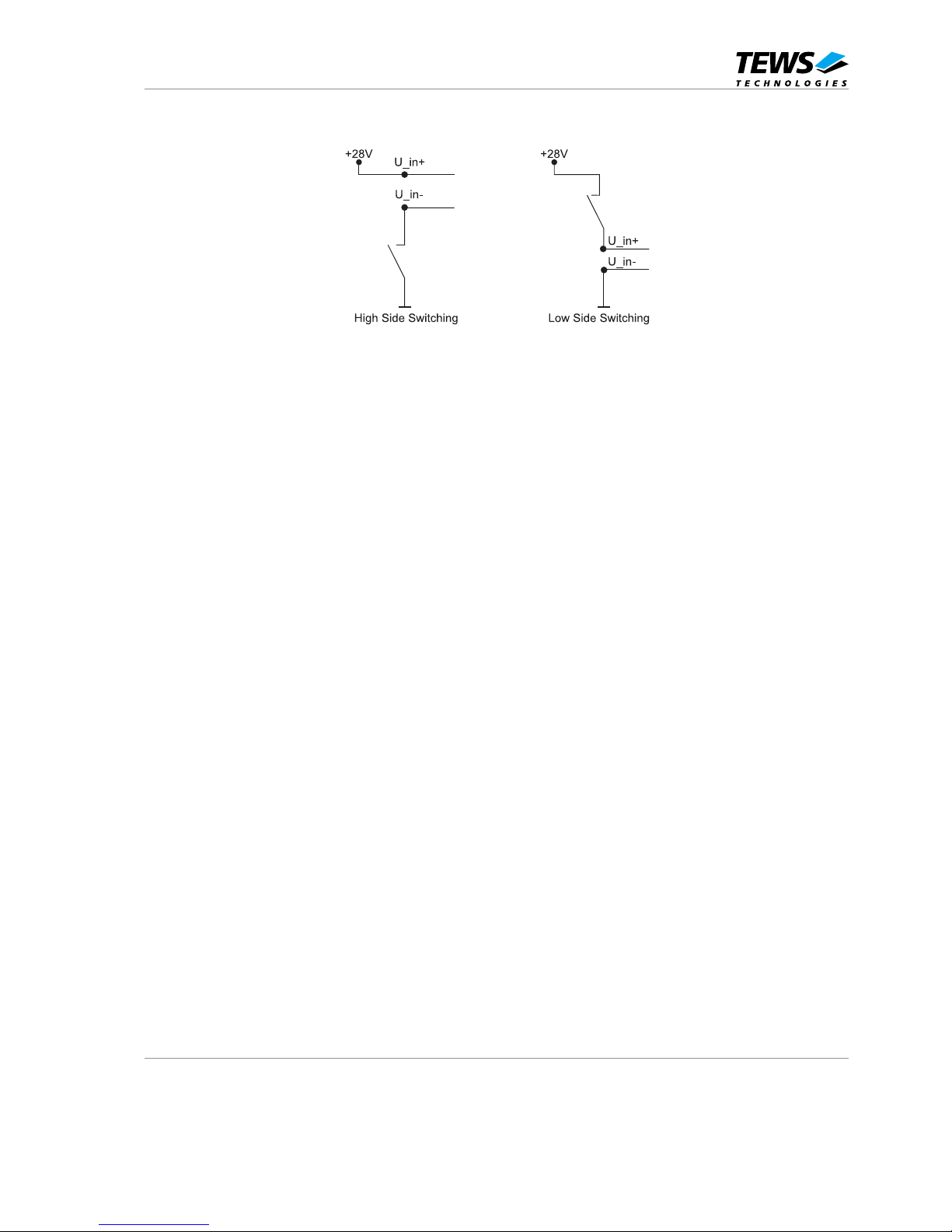
The input stage of the TIP606 is designed to sense high side or low side switching.
Figure 5-2 : High Side and Low Side Switching
Page 15
TIP606 User Manual Issue 1.3 Page 15 of 15
6 Pin Assignment – I/O Connector
Pin Signal Pin Signal
1 Input 1 + 26 Input 13 2 Input 1 - 27 Input 14 +
3 Input 2 + 28 Input 14 4 Input 2 - 29 Input 15 +
5 Input 3 + 30 Input 15 6 Input 3 - 31 Input 16 +
7 Input 4 + 32 Input 16 8 Input 4 - 33 Not used
9 Input 5 + 34 Not used
10 Input 5 - 35 Not used
11 Input 6 + 36 Not used
12 Input 6 - 37 Not used
13 Input 7 + 38 Not used
14 Input 7 - 39 Not used
15 Input 8 + 40 Not used
16 Input 8 - 41 Not used
17 Input 9 + 42 Not used
18 Input 9 - 43 Not used
19 Input 10 + 44 Not used
20 Input 10 - 45 Not used
21 Input 11 + 46 Not used
22 Input 11 - 47 Not used
23 Input 12 + 48 Not used
24 Input 12 - 49 GND_I
25 Input 13 + 50 GND_I
Figure 6-1 : Pin Assignment I/O Connector
 Loading...