

Page 1

The Embedded I/O Company
TIP255
2 Mbytes SRAM Memory
with Battery Backup
Version 1.0 Revision C
User Manual
Issue 1.0.6
September 2009
TEWS TECHNOLOGIES GmbH
Am Bahnhof 7 25469 Halstenbek, Germany
Phone: +49 (0) 4101 4058 0 Fax: +49 (0) 4101 4058 19
e-mail: [email protected]
www.tews.com
Page 2

TIP255 User Manual Issue 1.0.6 Page 2 of 13
TIP255-10
2 Mbytes SRAM memory with battery backup
TIP255-10-ET
2 MB of SRAM Memory with battery backup,
operating temperature -40°C to +85°C
This document contains information, which is
proprietary to TEWS TECHNOLOGIES GmbH. Any
reproduction without written permission is forbidden.
TEWS TECHNOLOGIES GmbH has made any
effort to ensure that this manual is accurate and
complete. However TEWS TECHNOLOGIES GmbH
reserves the right to change the product described
in this document at any time without notice.
TEWS TECHNOLOGIES GmbH is not liable for any
damage arising out of the application or use of the
device described herein.
Style Conventions
Hexadecimal characters are specified with prefix 0x,
i.e. 0x029E (that means hexadecimal value 029E).
For signals on hardware products, an ‚Active Low’ is
represented by the signal name with # following, i.e.
IP_RESET#.
Access terms are described as:
W Write Only
R Read Only
R/W Read/Write
R/C Read/Clear
R/S Read/Set
©2002-2009 by TEWS TECHNOLOGIES GmbH
All trademarks mentioned are property of their respective owners.
Page 3

TIP255 User Manual Issue 1.0.6 Page 3 of 13
Issue Description Date
1.0 First Issue February 2002
1.1 New Module Revision B March 2002
1.2 New Module Revision C October 2003
1.3 Added Security Warning (Lithium Battery) August 2004
1.4 New Module Version TIP255-10-ET April 2005
1.5 New address TEW S LLC September 2006
1.0.6 New User Manual Issue Notation September 2009
Page 4

TIP255 User Manual Issue 1.0.6 Page 4 of 13
Table of Contents
1 PRODUCT DESCRIPTION.........................................................................................6
2 TECHNICAL SPECIFICATION...................................................................................7
3 ID PROM CONTENTS................................................................................................8
4 IP ADDRESSING........................................................................................................9
4.1 I/O Addressing.................................................................................................................................9
4.1.1 SRAM Control Register (CR)................................................................................................9
4.1.2 SRAM Status Register (SR) .................................................................................................9
4.1.3 Interrupt Vector Register (INTVEC)....................................................................................10
4.2 Memory Addressing......................................................................................................................10
5 MODULE INSTALLATION .......................................................................................11
5.1 Security Warning (Lithium Battery).............................................................................................11
5.2 Jumper Configuration...................................................................................................................12
5.2.1 Jumper Settings..................................................................................................................12
6 PIN ASSIGNMENT ...................................................................................................13
Page 5

TIP255 User Manual Issue 1.0.6 Page 5 of 13
List of Figures
FIGURE 1-1 : BLOCK DIAGRAM......................................................................................................................6
FIGURE 5-1 : JUMPER CONFIGURATION....................................................................................................12
List of Tables
TABLE 2-1 : TECHNICAL SPECIFICATION.....................................................................................................7
TABLE 3-1 : ID PROM CONTENTS..................................................................................................................8
TABLE 4-1 : REGISTER SET............................................................................................................................9
TABLE 4-2 : SRAM CONTROL REGISTER (CR).............................................................................................9
TABLE 4-3 : SRAM STATUS REGISTER (SR) ................................................................................................9
TABLE 6-1 : PIN ASSIGNMENT J1................................................................................................................13
Page 6
TIP255 User Manual Issue 1.0.6 Page 6 of 13
1 Product Description
The TIP255 is an Industr yPack® compatible module that offers an easy and reliable way to implement
2 Mbytes of SRAM memory with battery backup.
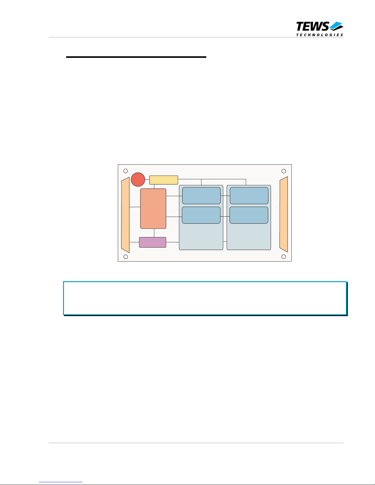
The 2 Mbyte SRAM is organized in two banks, each bank is providing 512k x 16 bit memory. For all
SRAM devices battery backup is provided by an on board lithium cell. During normal operation
(standard 5V supply applied to the SRAM’s) the capacity of the lithium cell is monitored every 24
hours by the battery monitor device. In addition an interrupt is generated if the battery voltage is too
low. The battery monitor device switches the power supply of the SRAM’s from the standard 5V to the
battery if the 5V drop below the threshold level of the battery monitor device. At this point any active
access to the SRAM’s is executed correctly within 1.5 µs. After this time further accesses to the
SRAM’s are not possible.
Accesses to the TIP255 SRAM memory occur within the IP memory space. The IP I/O space holds the
Interrupt Control Register, the Interrupt and Battery Status Register and the Interrupt Vector Register.
Industry Pack I/O Interface
Pack logic InterfaceIndustry
ID-PROM
4MbitSRAM
(512 Kbyte)
Local
Control
Logic
Bank1
1 Mbyte SRAM
16 bit wide
Bank2
Local +3.3V
1 Mbyte SRAM
16 bit wide
4 Mbit SRAM
(512 Kbyte)
4 Mbit SRAM
(512 Kbyte)
4 Mbit SRAM
(512 Kbyte)
Nonvolatile
SRAM Controller
Battery
Figure 1-1 : Block Diagram
CAUTION! - This system contains a lithium battery. Lithium batteries may explode if
mishandled.
Please refer to chapter “Security Warning (Lithium Battery)”.
Page 7

TIP255 User Manual Issue 1.0.6 Page 7 of 13
2 Technical Specification
IP Interface
Single Size IndustryPack® Logic Interface
ID PROM supports auto-configuration
Module Specific Data
Memory Size
2 Mbytes SRAM Memory
Memory Organization
2 banks of 1 Mbyte
Data Width
16 bit
Wait States
No wait states
Interrupts
IntReq0 on battery low
SRAM
CMOS SRAM Chip
4 x 512x8 low-low power SRAM
Battery
On Board Battery Type
CR2430 Lithium Cell (285mAh capacity)
Battery Fault Voltage
2.6V typical
Battery Lifetime (caused by
self discharching effects)
@+25°C : approx. 8 years
@+45°C : approx. 4 years
Battery Current in
Memory Backup Mode
4µA typical @ +25°C
Min. Data Retention Voltage
2.0V
5V Power Failure Threshold
4.37V typical
I/O Interface
No connections to IP I/O connector
Physical Data
Power Requirements
65mA typical @ + 5V DC
Temperature Range
Operating
Storage
0 °C to +70 °C
-40°C to +85°C (TIP255-10-ET)
-55 °C to +125 °C
MTBF
550000 h
Humidity
5 – 95 % non-condensing
Table 2-1 : Technical Specification
Page 8

TIP255 User Manual Issue 1.0.6 Page 8 of 13
3 ID PROM Contents
ADDRESS FUNCTION CONTENTS
0x01 ASCII ‘I’ 49
0x03 ASCII ‘P’ 50
0x05 ASCII ‘A’ 41
0x07 ASCII ‘C’ 43
0x09 Manufacturer ID B3
0x0B Model Number 31
0x0D Revision 10
0x0F RESERVED 00
0x11 Driver-ID Low – Byte 00
0x13 Driver-ID High – Byte 00
0x15 Number of bytes used 0C
0x17 Check Sum 9C
Table 3-1 : ID PROM Contents
Page 9

TIP255 User Manual Issue 1.0.6 Page 9 of 13
4 IP Addressing
4.1 I/O Addressing
The complete register set of the TIP255-10 is accessible in the I/O space of the IP.
Address Symbol Description Size (Bit) Access
0x01 CR Interrupt Control Register 8 R/W
0x03 SR Interrupt and Battery Status Register 8 R/W
0x05 INTVEC Interrupt Vector Re gister 8 R/W
Table 4-1 : Register Set
4.1.1 SRAM Control Register (CR)
The CR is a read/write register to enable interrupt generation of the TIP255.
Bit Symbol Description Access
7:1 N/A
0
INT
ENA
Interrupt Enable
1 = an interrupt is always initiated, whenever the battery
voltage falls below the reference voltage of the
nonvolatile SRAM controller (V
ref
=2.6V typical).
R/W
Table 4-2 : SRAM Control Register (CR)
4.1.2 SRAM Status Register (SR)
The SR is a read/write register to observe battery and interrupt status of the TIP255.
Bit Symbol Description Access
7:2 N/A
1 IS Interrupt Status
1 = if an interrupt is pending. This bit is reset to ‘0’ by a write
access to this register with any data.
R/W
0 BS Battery Status
1 = the battery voltage has fallen below the reference voltage
of V
ref
=2.6V typical. In this case the battery will soon
reach end-of-live. For reliable function of the battery
backup, the battery should be replaced.
R/W
Table 4-3 : SRAM Status Register (SR)
Page 10

TIP255 User Manual Issue 1.0.6 Page 10 of 13
4.1.3 Interrupt Vector Register (INTVEC)
The INTVEC is a read/write register. It must be loaded by software with the desired interrupt vector
value, when interrupts shall be used.
A reset will set the INTVEC to the default value of 0x00.
4.2 Memory Addressing
Access to the TIP255 SRAM is simply done by reading or writing data to the address space where the
TIP255 memory is mapped in the processors memory space. 8 bit and 16 bit accesses are supported.
Page 11

TIP255 User Manual Issue 1.0.6 Page 11 of 13
5 Module Installation
5.1 Security Warning (Lithium Battery)
CAUTION! - This system contains a lithium battery. Lithium batteries may explode if
mishandled.
Please observe the following warnings strictly. If misused, the battery may explode or leak,
causing injury or damage to the equipment.
• Keep batteries out of the reach of children. In case of ingestion of a cell or battery, the person
involved should seek medical assistance promptly.
• The batteries must be inserted into the equipment with the correct polarity (+ and -).
• Do not use metallic or other conductive extraction tools to replace the batteries.
• Do not attempt to revive used batteries by heating, charging or other means.
• Do not dispose of batteries in fire. Do not dismantle batteries.
• Do not short circuit batteries.
• Do not expose batteries to high temperatures, moisture or direct sunlight.
• Do not place batteries on a conductive surface (anti-static work mat, packaging bag or form trays)
as it can cause the battery to short.
CAUTION ! Danger of explosion if battery is incorrectly replaced. Replace only with the same or
equivalent type recommended by the manufacturer. Dispose of used batteries according to the
manufacturer's instructions.
Page 12
TIP255 User Manual Issue 1.0.6 Page 12 of 13
5.2 Jumper Configuration
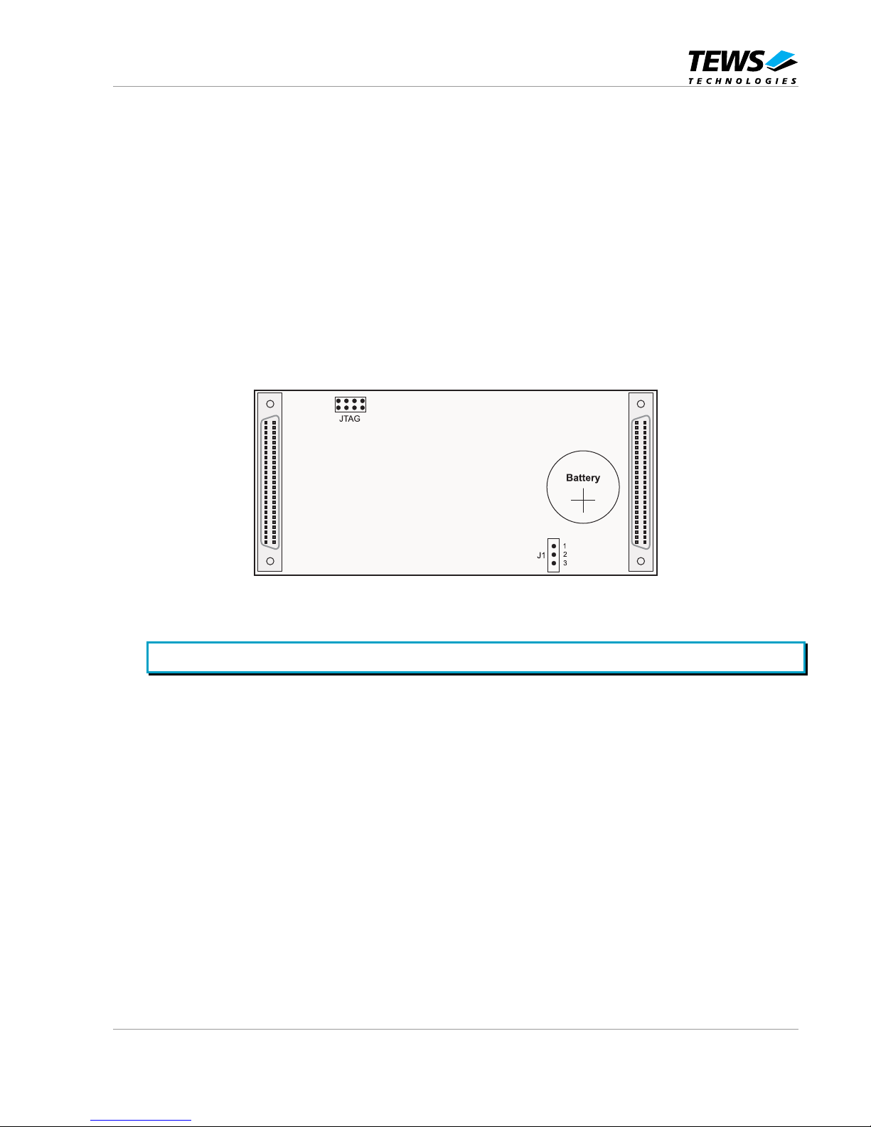
For the use of the battery backup support the enclosed battery must be unpacked and clipped into the
battery holder. With the default jumper configuration the battery backup support of the TIP255 is now
active.
If the battery support of the TIP255 is not used, jumper J1 must be switched to position 1-2.
5.2.1 Jumper Settings
J1: 1-2 Battery backup support disabled
2-3 Battery backup support enabled
Figure 5-1 : Jumper Configuration
By factory configuration the battery backup support is enabled (J1: 2-3).
Page 13

TIP255 User Manual Issue 1.0.6 Page 13 of 13
6 Pin Assignment
The table shows the complete IP J1 logic interface pin assignment. Some of these signals are not
used by the TIP255-10.
Pin Signal Pin Signal
1 GND 26 GND
2 CLK 27 +5V
3 Reset# 28 R/W#
4 D0 29 IDSel#
5 D1 30 DMAReq0#
6 D2 31 MemSel#
7 D3 32 DMAReq1#
8 D4 33 IntSel#
9 D5 34 DMAAck#
10 D6 35 IOSel#
11 D7 36 Reserved
12 D8 37 A1
13 D9 38 DMAEnd#
14 D10 39 A2
15 D11 40 Error#
16 D12 41 A3
17 D13 42 IntReq0#
18 D14 43 A4
19 D15 44 IntReq1#
20 BS0# 45 A5
21 BS1# 46 Strobe#
22 -12V 47 A6
23 +12V 48 ACK#
24 +5V 49 Reserved
25 GND 50 GND
Table 6-1 : Pin Assignment J1
 Loading...