


73S8014R
Smart Card Interface
Simplifying System Integration™
September 2008
DATA SHEET
DESCRIPTION
The Teridian 73S8014R is a single smart card (ICC) interface
circuit, firmware compatible with 8024-type devices for
configurations where only asynchronous cards must be
supported. It is derived from the 73S8024RN industrystandard electrical interface. The 73S8014R has been
optimized to match most of the typical Set-Top-Box / A/V
Conditional Access applications. Optimization essentially
involved a smaller pin-count, support for single I/O, and
maximum card current of 65mA (ISO-7816 / EMV
compliance).
The 73S8014R interfaces with the host processor through the
same bus (digital I/Os) as the 73S8024RN, which is
compatible with any other 8024-type IC. As a result, the
73S8014R is a very attractive cost-reduction path from
traditional 8024 ICs. The 73S8014R has been designed to
provide full electrical compliance with ISO 7816-3 and EMV
4.0 specifications.
Interfacing with the system controller is done through a
control bus, composed of digital inputs to control the
interface, and one interrupt output to inform the system
controller of the card presence and faults.
The card clock can be generated by an on-chip oscillator
using an external crystal or by connection to an externally
supplied clock signal.
The 73S8014R incorporates an ISO 7816-3
activation/deactivation sequencer that controls the card
signals. Level-shifters drive the card signals with the
selected card voltage (3V or 5V), coming from an internal
Low Drop-Out (LDO) voltage regulator. This LDO regulator is
powered by a dedicated power supply input V
circuitry is powered separately by a digital power supply V
With its embedded LDO regulator, the 73S8024RN is a
cost-effective solution for any application where a 5V
(typically -5% +10%) power supply is available.
Emergency card deactivation is initiated upon card extraction
or upon any fault detected by the protection circuitry. The
fault can be a card over-current, VCC undervoltage or power
supply fault (V
). The card over-current circuitry is a true
DD
current detection function, as opposed to V
detection, as usually implemented in non-Teridian 8024
interface ICs.
The V
voltage fault has a threshold voltage that can be
DD
adjusted with an external resistor network. It allows
automated card deactivation at a customized V
threshold value. It can be used, for instance, to match the
system controller operating voltage range.
. Digital
PC
voltage drop
CC
voltage
DD
DD
.
APPLICATIONS
• Set-Top-Box Conditional Access and Pay-per-View
• General purpose smart card readers
ADVANTAGES
• Same advantages as the Teridian 73S80xxR family:
VCC card generated by an LDO regulator
Very low power dissipation (saves up to 1/2W)
Fewer external components are required
Better noise performance
• True card over-current detection
• Firmware compatibility with all 8024 ICs
• Small format 20SO package
FEATURES
• Card Interface:
Complies with ISO 7816-3 and EMV 4.0
Supports 3V / 5V cards
ISO 7816-3 Activation / Deactivation sequencer
Automated deactivation upon hardware fault (i.e. upon
drop on V
The V
be externally adjusted
Over-current detection 130mA max
Card CLK clock frequency up to 20MHz
• System Controller Interface:
3 Digital inputs control the card activation /
deactivation, card reset and card voltage
2 Digital inputs control the card clock frequency
1 Digital output, interrupt to the system controller,
reports to the host the card presence and faults
Crystal oscillator or host clock, up to 27MHz
• Regulator Power Supply:
4.75V to 5.5V
• Digital Interfacing: 2.7V to 5.5V
• 6kV ESD protection on the card interface
• Package: SO 20-pin
• RoHS compliant (6/6) lead-free package
power supply or card overcurrent)
DD
voltage supervisor threshold value (fault) can
DD
Rev. 1.0 © 2008 Teridian Semiconductor Corporation 1
73S8014R Data Sheet DS_8014R_012
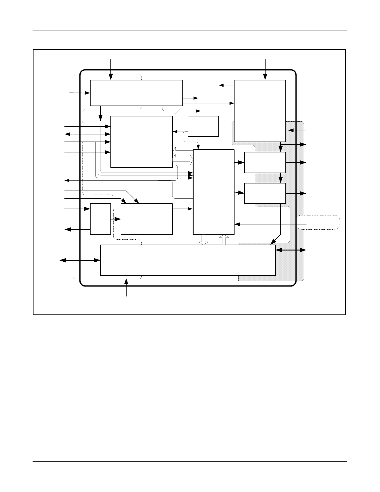
FUNCTIONAL DIAGRAM
VDD VPC
VDDF_ADJ
CMDVCC
RSTIN
5V/#V
TEST
OFF
CKDIV1
CKDIV2
XTALIN
XTALOUT
IOUC
vdd circui ts
INTERNAL POWER SUPPLY
VOLTAGE REFERENCE
VPD - internal supply
CONTROLLER
REGISTERS
FAULT LOGIC
XTAL
OSC
GENERATION
vdd circuits
VDD FAULT
bias currents
1.5MHz
AND
CLOCK
CLOCK
SMART CARD I/O BUFFER
VCC FAULT
vref
R-C
OSC.
SC
SEQUENCER
LDO
REGULATOR
RESET
BUFFER
CLOCK
BUFFER
GND
VCC
RST
CLK
VDD CKT
PRES
I/O
vcc circuits
GND
Figure 1: 73S8014R Block Diagram
2 Rev. 1.0

DS_8014R_012 73S8014R Data Sheet
Table of Contents
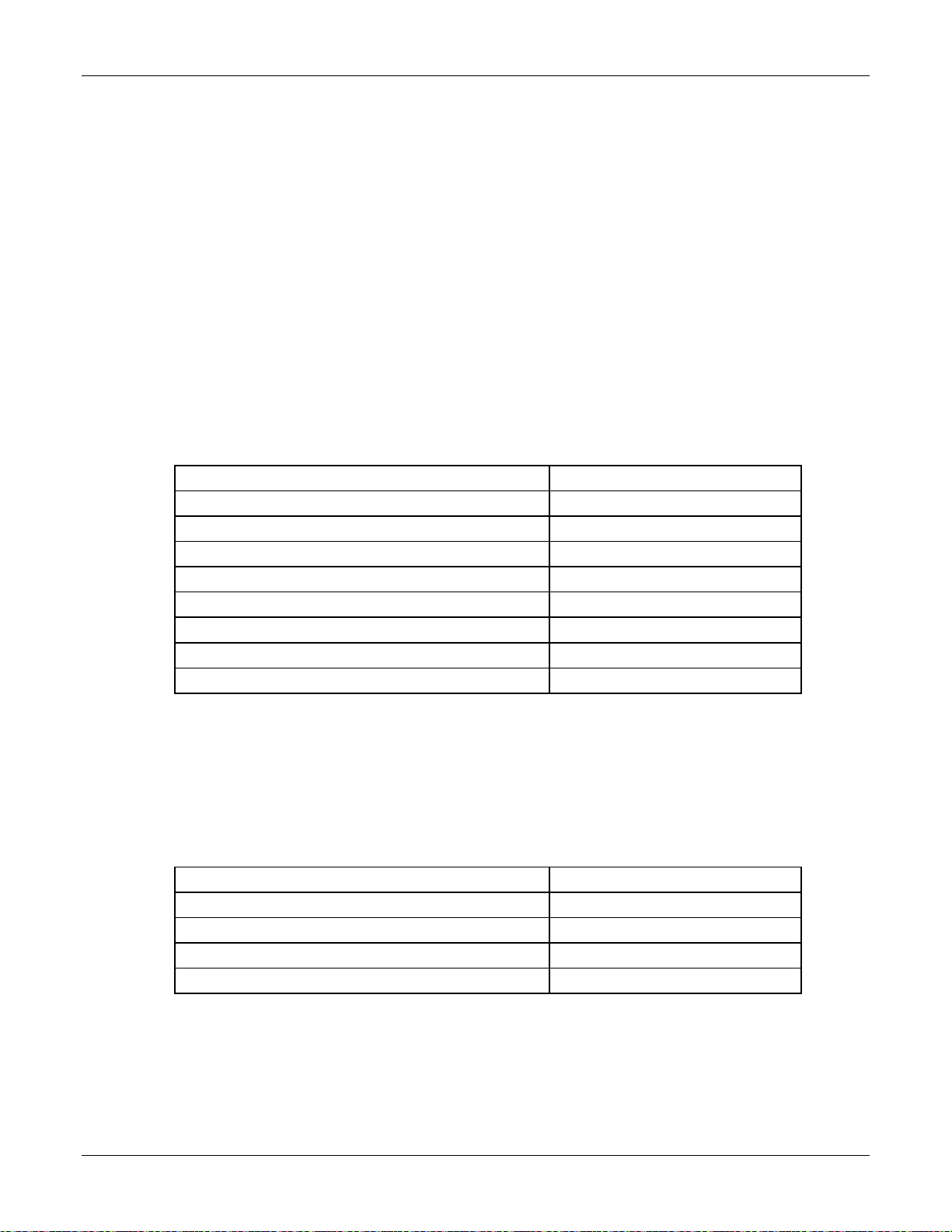
1 Pinout ................................................................................................................................................................ 5
2 Electrical Specifications .................................................................................................................................. 8
2.1 Absolute Maximum Ratings ........................................................................................................................ 8
2.2 Recommended Operating Conditions ......................................................................................................... 8
2.3 Package Thermal Parameters .................................................................................................................... 9
2.4 Smart Card Interface Requirements ........................................................................................................... 9
2.5 Characteristics: Digital Signals.................................................................................................................. 11
2.6 DC Characteristics .................................................................................................................................... 12
2.7 Voltage Fault Detection Circuits ................................................................................................................ 13
3 Applications Information ............................................................................................................................... 14
3.1 Example 73S8014R Schematics .............................................................................................................. 14
3.2 System Controller Interface ....................................................................................................................... 16
3.3 Power Supply and Voltage Supervision .................................................................................................... 16
3.4 Card Power Supply ................................................................................................................................... 17
3.5 On-Chip Oscillator and Card Clock ........................................................................................................... 17
3.6 Activation Sequence ................................................................................................................................. 18
3.7 Deactivation Sequence ............................................................................................................................. 19
3.8 Fault Detection and OFF ........................................................................................................................... 20
3.9 I/O Circuitry and Timing ............................................................................................................................ 20
4 Equivalent Circuits ......................................................................................................................................... 22
5 Mechanical Drawing ....................................................................................................................................... 27
6 Ordering Information ..................................................................................................................................... 28
7 Related Documentation ................................................................................................................................. 28
8 Contact Information ....................................................................................................................................... 28
Rev. 1.0 3

73S8014R Data Sheet DS_8014R_012
Figures
Figure 1: 73S8014R Block Diagram .......................................................................................................................... 2
Figure 2: 73S8014R 20-SOP Pin Out ........................................................................................................................ 5
Figure 3: 73S8014R – Typical Application Schematic ............................................................................................ 15
Figure 4: Activation Sequence – RSTIN Low When CMDVCC Goes Low ............................................................. 18
Figure 5: Activation Sequence – RSTIN High When CMDVCC Goes Low ............................................................. 19
Figure 6: Deactivation Sequence ............................................................................................................................ 19
Figure 7: Timing Diagram – Management of the Interrupt Line OFF ...................................................................... 20
Figure 8: I/O and I/OUC State Diagram................................................................................................................... 21
Figure 9: I/O – I/OUC Delays – Timing Diagram ..................................................................................................... 21
Figure 10: Open Drain type – OFF .......................................................................................................................... 22
Figure 11: Power Input/Output Circuit, VDD, VPC, VCC ........................................................................................ 22
Figure 12: Smart Card CLK Driver Circuit ............................................................................................................... 23
Figure 13: Smart Card RST Driver Circuit ............................................................................................................... 23
Figure 14: Smart Card IO Interface Circuit .............................................................................................................. 24
Figure 15: Smart Card IOUC Interface Circuit ......................................................................................................... 24
Figure 16: General Input Circuit .............................................................................................................................. 25
Figure 17: Oscillator Circuit ..................................................................................................................................... 25
Figure 18: VDDF_ADJ ............................................................................................................................................. 26
Figure 19: Mechanical Drawing 20-Pin SO Package .............................................................................................. 27
Tables
Table 1: 73S8014R 20-Pin SOP Pin Definitions ....................................................................................................... 6
Table 2: Absolute Maximum Device Ratings ............................................................................................................. 8
Table 3: Recommended Operating Conditions ......................................................................................................... 8
Table 4: Package Thermal Parameters ..................................................................................................................... 9
Table 5: DC Smart Card Interface Requirements ..................................................................................................... 9
Table 6: Digital Signals Characteristics ................................................................................................................... 11
Table 7: DC Characteristics ..................................................................................................................................... 12
Table 8: Voltage Fault Detection Circuits ................................................................................................................ 13
Table 9: Order Numbers and Packaging Marks ...................................................................................................... 28
4 Rev. 1.0
DS_8014R_012 73S8014R Data Sheet
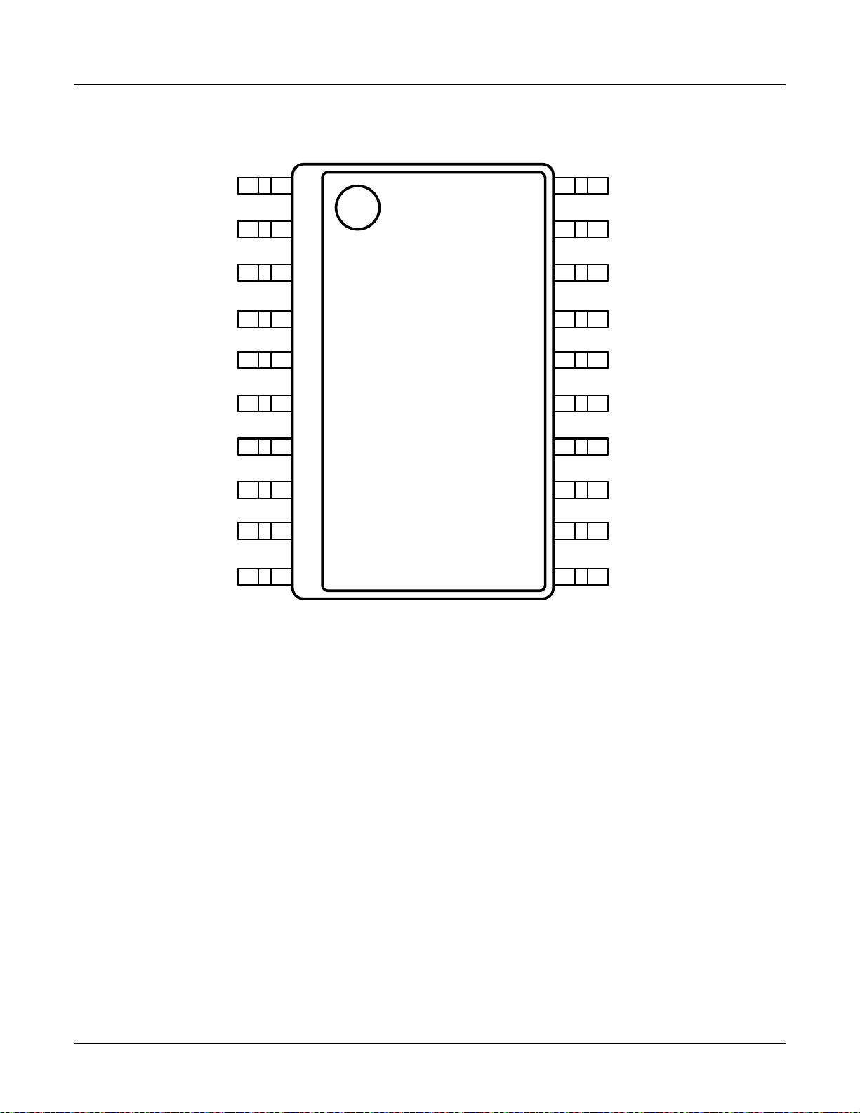
1 Pinout
The 73S8014R is supplied as a 20-pin SO package.
OFF
RSTIN
I/OUC
VPC
CLKDIV2
1
2
3
4
5
20
19
18
17
16
CLKDIV1
PRES
VCC
CLK
GND
73S8014R
CMDVCC
5V/#V
GND
XTALIN
XTALOUT
6
7
8
9
10
Figure 2: 73S8014R 20-SOP Pin Out
15
14
13
12
11
RST
I/O
VDD
VDDF_ADJ
GND
Rev. 1.0 5
73S8014R Data Sheet DS_8014R_012
Table 1 provides the 73S8014R pin names, pin numbers, type, equivalent circuits and descriptions.
Table 1: 73S8014R 20-Pin SOP Pin Definitions
Pin Name
Pin
Number
Type
Equivalent
Circuit
Description
Card Interface
I/O 14 IO Figure 14
Card I/O: Data signal to/from card. Includes an 11k pull-up
resistor to V
CC.
RST 15 O Figure 13 Card reset: provides reset (RST) signal to card.
Card clock: provides clock signal (CLK) to card. The rate of this
CLK 17 O Figure 12
clock is determined by the external crystal frequency or frequency
of the external clock signal applied on XTALIN and CLKDIV
selections.
PRES 19 I Figure 16
Card Presence switch: active high indicates card is present.
Includes a high-impedance pull-down current source.
Card power supply – logically controlled by sequencer, output of
VCC 18 PSO Figure 11
LDO regulator. Requires an external filter capacitor to the card
GND.
GND 16 GND – Card ground.
Host Processor Interface
Command VCC (negative assertion): Logic low on this pin causes
CMDVCC
6 I Figure 16
the LDO regulator to ramp the V
supply to the card and initiates
CC
a card activation sequence, if a card is present.
5 volt / 3 volt card selection: Logic one selects 5 volts for VCC and
card interface, logic low selects 3 volt operation. When the part is
5V/#V 7 I Figure 16
to be used with a single card voltage, this pin should be tied to
either GND or V
. However, it includes a high impedance pull-up
DD
resistor to default this pin high (selection of 5V card) when not
connected. This pin shall not be changed when CMDVCC is low.
Sets the divide ratio from the XTAL oscillator (or external clock
input) to the card clock. These pins include a pull-up resistor for
CLKDIV1 and CLKLDIV2 to provide a default rate of divide by
two.
CLKDIV1
CLKDIV2
20
5
I Figure 16
CLKDIV1 CLKDIV2 CLOCK RATE
0 0 XTALIN/8
0 1 XTALIN/4
1 1 XTALIN/2
1 0 XTALIN
Interrupt signal to the processor. Active Low - Multi-function
OFF 1 O Figure 10
indicating fault conditions and card presence. Open drain output
configuration – It includes an internal 20kΩ pull-up to V
DD.
RSTIN 2 I Figure 16 Reset Input: This signal is the reset command to the card.
I/OUC 3 IO Figure 15
System controller data I/O to/from the card. Includes an 11K
pull-up resistor to V
DD.
6 Rev. 1.0
DS_8014R_012 73S8014R Data Sheet
Miscellaneous Inputs and Outputs
Crystal oscillator input: can either be connected to crystal or
XTALIN 9 Figure 17
driven as a source for the card clock. Note: When not using the
crystal, the capacitors must be removed.
Crystal oscillator output: connected to crystal. Left open if
XTALOUT 10 Figure 17
XTALIN is being used as external clock input. Note: When not
using the crystal, the capacitors must be removed.
VDD fault threshold adjustment input: this pin can be used to adjust
VDDF_ADJ 12 Figure 18
the V
value (that controls deactivation of the card). Must be
DDF
left open if unused.
Power Supply and Ground
VDD 13 PSO Figure 11
System interface supply voltage and supply voltage for internal
circuitry.
VPC 4 PSO Figure 11 LDO regulator power supply source.
GND 8, 11 GND – Digital ground.
Rev. 1.0 7
73S8014R Data Sheet DS_8014R_012
2 Electrical Specifications
This section provides the following:
Absolute maximum ratings
Recommended operating conditions
Package thermal parameters
Smart card interface requirements
Digital signals characteristics
DC Characteristics
Voltage Fault Detection Circuits
2.1 Absolute Maximum Ratings
Table 2 lists the maximum operating conditions for the 73S8014R. Permanent device damage may occur if
absolute maximum ratings are exceeded. Exposure to the extremes of the absolute maximum rating for extended
periods may affect device reliability. The smart card interface pins are protected against short circuits to V
ground, and each other.
2.2 Recommended Operating Conditions
Table 2: Absolute Maximum Device Ratings
Parameter Rating
Supply Voltage VDD -0.5 to 6.0 VDC
Supply Voltage VPC -0.5 to 6.0 VDC
Input Voltage for Digital Inputs -0.3 to (VDD +0.5) VDC
Storage Temperature -60 to 150°C
Pin Voltage (except card interface) -0.3 to (VDD +0.5) VDC
Pin Voltage (card interface) -0.3 to (VCC + 0.5) VDC
ESD Tolerance – Card interface pins +/- 6kV
ESD Tolerance – Other pins +/- 2kV
*Note: ESD testing on smart card pins is HBM condition, 3 pulses, each polarity referenced to ground.
Note: Smart Card pins are protected against shorts between any combinations of Smart Card pins.
CC
,
Function operation should be restricted to the recommended operating conditions specified in Table 3.
Table 3: Recommended Operating Conditions
Parameter Rating
Supply Voltage VDD 2.7 to 5.5 VDC
Supply Voltage VPC 4.75 to 5.5 VDC
Ambient Operating Temperature -40°C to +85°C
Input Voltage for Digital Inputs 0V to VDD + 0.3V
8 Rev. 1.0
DS_8014R_012 73S8014R Data Sheet
2.3 Package Thermal Parameters
Table 4 lists the 73S8014R Smart Card interface requirements.
Table 4: Package Thermal Parameters
Parameter Rating
20 SO
50
°C / W
2.4 Smart Card Interface Requirements
Table 5 lists the 73S8014R Smart Card interface requirements.
Table 5: DC Smart Card Interface Requirements
Symbol Parameter Condition Min Nom Max Unit
Card Power Supply (VCC) Regulator
General conditions, -40°C < T < 85°C, 4.75V < VPC < 5.5V, 2.7V < VDD < 5.5V
Card supply voltage
VCC
V
V
CCrip
I
CCmax
I
I
CCF
including ripple and
noise
Card supply output
current
Ripple f
CC
fault current
CC
Inactive mode
Inactive mode, ICC = 1mA
Active mode; ICC <65mA; 5V
Active mode; ICC <65mA; 3V
Active mode; ICC <40mA; 1.8V
Active mode; single pulse of 100mA for
2μs; 5 volt, fixed load = 25mA
Active mode; single pulse of 100mA for
2μs; 3v, fixed load = 25mA
Active mode; current pulses of 40nAs
with peak |I
t <400ns; 5V
Active mode; current pulses of 40nAs
with peak |I
t <400ns; 3V
= 20K – 200MHz 350 mV
RIPPLE
Static load current, V
as selected
| <200mA,
CC
| <200mA,
CC
>4.6V or 2.7V
CC
-0.1
-0.1
4.65
2.85
1.68
4.6
2.76
4.6
2.7
65 mA
70
0.1 V
0.4 V
5.25 V
3.15 V
1.92 V
5.25 V
3.2 V
5.25 V
3.15 V
130 mA
V
V
SR
VSF V
C
F
Rev. 1.0 9
slew rate, rise
CC
slew rate, fall
CC
External filter cap
to GND)
(V
CC
= 1.0μF on VCC
C
F
= 1.0μF on VCC
C
F
CF should be ceramic with low ESR
(<100mΩ).
0.06 0.150 0.30
0.075 0.150 0.60
0.5 1.0 1.5
V/μs
V/μs
μF

73S8014R Data Sheet DS_8014R_012
Symbol Parameter Condition Min Nom Max Unit
Interface Requirements – Data Signals: I/Oand host interfaces: I/OUC.
I
SHORTL
V
OH
, I
, and V
SHORTH
Output level, high (I/O)
Output level, high (I/OUC)
requirements do not pertain to I/OUC.
INACT
I
=0 0.9 V
OH
IOH = -40μA
I
=0 0.9 VDD
OH
IOH = -40μA
0.75 V
0.75 V
CC
CC
DD
VCC+0.1 V
VCC+0.1 V
VDD+0.1 V
VDD+0.1 V
Output level, low (I/O)
VOL
Output level, low (I/OUC) IOL=1mA
Input level, high (I/O) 0.6 V
VIH
Input level, high (I/OUC) 1.8
Input level, low (I/O) -0.15
VIL
Input level, low (I/OUC) -0.3
I
= 0
V
INACT
I
Input leakage VIH = VCC
LEAK
IIL Input current, low VIL = 0
I
SHORTL
I
SHORTH
tR, tF Output rise time, fall times
Output voltage when outside
of session
Short circuit output current
Short circuit output current
OL
IOL = 1mA
For output low,
shorted to V
through 33 Ω
For output high,
shorted to ground
through 33 Ω
= 80pF, 10% to
C
L
90%.
CC
CC
0.15 VCC V
0.3 V
VCC+0.30
VDD + 0.3
0.2 VCC V
0.8 V
0.1 V
0.3 V
10
0.65 mA
15 mA
15 mA
100 ns
V
V
μA
tIR, tIF Input rise, fall times 1
RPU Internal pull-up resistor
FD
Maximum data rate 1
MAX
T
FDIO
T
15
RDIO
CIN Input capacitance 10 pF
10 Rev. 1.0
Delay, I/O to I/OUC,
I/OUC to I/O, (respectively
falling edge to falling edge
and rising edge to rising
edge)
Output stable for
>400ns
Edge from master to
slave, measured at
50%
8 11 14
60 100 200 ns
μs
kΩ
MHz
ns

DS_8014R_012 73S8014R Data Sheet
Symbol Parameter Condition Min Nom Max Unit
Reset and Clock for card interface, RST, CLK
V
Output level, high
OH
I
=-200μA
OH
0.9 V
CC
VCC V
VOL Output level, low
V
INACT
I
RST_LIM
I
CLK_LIM
CLK
SR3V
CLK
SR5V
tR, tF Output rise time, fall time
δ
Output voltage when outside
of session
Output current limit, RST 30 mA
Output current limit, CLK 70 mA
CLK slew rate Vcc = 3V 0.3
CLK slew rate Vcc = 5V 0.5
C
CL = 200pF for RST,
Duty cycle for CLK
=200μA
I
OL
I
= 0
OL
IOL = 1mA
= 35pF for CLK,
L
10% to 90%
10% to 90%
C
=35pF,
L
F
≤ 20MHz
CLK
2.5 Characteristics: Digital Signals
Table 6 lists the 73S8014R digital signals characteristics.
Table 6: Digital Signals Characteristics
0
45
0.15 VCC V
0.1 V
0.3 V
V/ns
V/ns
8 ns
100 ns
55 %
Symbol Parameter Condition Min Nom Max Unit
Digital I/O except for XTALIN and XTALOUT
VIL Input Low Voltage -0.3
VIH Input High Voltage 1.8
VOL Output Low Voltage IOL = 2mA
VOH Output High Voltage IOH = -1mA VDD - 0.45
R
Pull-up resistor, OFF 16 20 24
OUT
|I
| Input Leakage Current GND < VIN < VDD -5
IL1
0.8 V
VDD + 0.3 V
0.45 V
V
kΩ
5 μA
Rev. 1.0 11

73S8014R Data Sheet DS_8014R_012
Oscillator (XTALIN) I/O Parameters
V
Input Low Voltage - XTALIN -0.3
ILXTAL
V
Input High Voltage - XTALIN 0.7 VDD
IHXTAL
I
ILXTAL
f
MAX
δin
Input Current -
XTALIN
Max freq. Osc or external
clock
External input duty cycle limit
GND < VIN < V
27 MHz
t
R/F < 10% fIN,
45% <
δ
CLK
< 55%
DD
-30
48
0.3 VDD V
VDD+0.3 V
30 μA
52 %
2.6 DC Characteristics
Table 7 lists the 73S8014R DC characteristics.
Table 7: DC Characteristics
Symbol Parameter Condition Min Nom Max Unit
12 MHz XTAL 2.7 7.0
IDD
Supply Current
IPC Supply Current
V
supply current when
I
PCOFF
PC
= 0
V
CC
Ext CLK,
VDD = 2.7 – 3.6V,
VCC Off
Ext CLK,
VDD = 2.7 – 3.6V,
VCC On
Ext CLK,
VDD = 4.5 – 5.5V,
VCC Off
Ext CLK,
VDD = 4.5 – 5.5V,
VCC On
on, ICC=0
V
CC
I/O, AUX1,
AUX2=high,
Clock not toggling
CMDVCC High
mA
mA
1.7
mA
2.2
2.7 mA
3 mA
450 700
345 650
μA
μA
12 Rev. 1.0

DS_8014R_012 73S8014R Data Sheet
2.7 Voltage Fault Detection Circuits
Table 8 lists the 73S8014R Voltage Fault Detection Circuits.
Table 8: Voltage Fault Detection Circuits
Symbol Parameter Condition Min Nom Max Unit
V
fault
DD
V
DDF
V
CCF
(VDD Voltage supervisor
threshold)
V
CC
(V
CC
threshold)
fault
Voltage supervisor
No external resistor
on VDDF_ADJ pin
= 5v
V
CC
VCC= 3v
2.15
4.6 V
2.4 V
2.7 V
Rev. 1.0 13

73S8014R Data Sheet DS_8014R_012
3 Applications Information
This section provides general usage information for the design and implementation of the 73S8014R. The
documents listed in Related Documentation provide more detailed information.
3.1 Example 73S8014R Schematics
Figure 3 shows a typical application schematic for the implementation of the 73S8014R. Note that minor changes
may occur to the reference material from time to time and the reader is encouraged to contact Teridian for the
latest information.
14 Rev. 1.0

DS_8014R_012 73S8014R Data Sheet
CLKDIV1_from_uC
OFF_interrupt_to_uC
RSTIN_from_uC
I/OUC_to/from_uC
CLKDIV2_from_uC
See
note 5
VDD
See NOTE 2
CMDVCC_from_uC
5V/#V_select_from_uC
See NOTE 3
External_clock_from uC
100nF
C4
VPC
10uF
C5
- OR -
C222pF
CRYSTAL
22pF
See NOTE 4
C3
Y1
1
2
3
4
5
6
7
8
9
10
R2
47K
OFF
RSTIN
I/OUC
VPC
CLKDIV2
CMDVCC
5V3V
GND
XTALIN
XTALOUT
73S8014R
CLKDIV1
PRES
VCC
CLK
GND
RST
I/O
VDD
VDDF_ADJ
TEST
20
19
18
17
16
15
14
13
12
11
R3
Rext2
R1
Rext1
See NOTE 1
C6
100nF
VDD
NOTES:
1) VDD = 2.7V to 5.5V DC.
2) VPC = 4.75V to 5.5V DC
3) Required if external clock from uP is used.
4) Required if crystal is used.
Y1, C2 and C3 must be removed if external clock is used.
5) R1 and R3 are external resistors that adjust the VDD
fault voltage. Can be left open.
VDD
Card detection
switch is
normally open
R4
10K
4
5
6
7
8
9
10
C8
SW-1
SW-2
Smart Card Connector
C4
I/O
VPP
GND
1
2
3
CLK
CLK track should be routed
RST
VCC
far from RST, I/O, C4 and
C8.
EMV & ISO7816=1uF
Low ESR (<100mohms) C1
C1
should be placed near the SC
connecter contact
Figure 3: 73S8014R – Typical Application Schematic
Rev. 1.0 15

73S8014R Data Sheet DS_8014R_012
3.2 System Controller Interface
Three digital inputs allow direct control of the card interface by the host. The 73S8014R is controlled as follows:
Pin CMDVCC: When asserted low, starts an activation sequence
Pin RSTIN: controls the card RST signal (when enabled by the sequencer)
Pin 5V/#V: Defines the card VCC voltage (5V when high and 3V when low)
Card clock frequency can be controlled by 2 digital inputs:
CLKDIV1 and CLKDIV2 define the division rate for the clock frequency, from the input clock frequency (crystal
or external clock)
Note: The maximum CLK frequency is 20MHz. Therefore, if using an input clock source greater than 20MHz, a
divisor rate of 2X or higher must be used.
Interrupt output to the host: As long as the card is not activated, the OFF pin informs the host about the card
presence only (Low = No card in the reader). When CMDVCC is asserted low (Card activation sequence
requested from the host), low level on OFF means a fault has been detected (e.g. card removal during card
session, voltage fault, or over-current fault) that automatically initiates a deactivation sequence.
3.3 Power Supply and Voltage Supervision
The 73S8014R smart card interface IC incorporates a LDO voltage regulator. The voltage output is controlled by
the digital input 5V/#V of the 73S8014R. This regulator is able to provide either 3V or 5V card voltage from the
power supply applied on the VPC pin. The voltage regulator can provide a current of at least 65mA on VCC for
both 3V and 5V that complies with EMV 4.0.
Digital circuitry is powered by the power supply applied on the VDD pin. VDD also defines the voltage range to
interface with the system controller. A card deactivation sequence is forced upon fault of any of this voltage
supervisor. One voltage supervisor constantly monitors the VDD voltage. It is used to initialize the ISO 7816-3
sequencer at power-on, and to deactivate the card at power-off or upon fault. The voltage threshold of the VDD
voltage supervisor is internally set by default to 2.33V nominal. However, it may be desirable, in some
applications, to modify this threshold value. The pin VDDF_ADJ is used to connect an external resistor R
ground to change the VDD fault voltage to another value, V
. The resistor value is defined as follows:
DDF
EXT
to
R
EXT
= 56kΩ /(V
- 2.33)
DDF
An alternative (more accurate) method of adjusting the VDD fault voltage is to use a resistive network of R3 from
the pin to supply and R1 from the pin to ground (see Figure 3). In order to set the new threshold voltage, the
equivalent resistance must be determined. This resistance value will be designated Kx. Kx is defined as
R1/(R1+R3). Kx is calculated as:
Kx = (2.789 / V
) - 0.6125 where VTH is the desired new threshold voltage.
TH
To determine the values of R1 and R3, use the following formulas.
R3 = 24000 / Kx R1 = R3*(Kx / (1 – Kx))
Taking the example above, where a V
fault threshold voltage of 2.7V is desired, solving for Kx gives:
DD
Æ Kx = (2.789 / 2.7) - 0.6125 = 0.42046.
Solving for R3 gives: Æ R3 = 24000 / 0.42046 = 57080.
Solving for R1 gives: Æ R1 = 57080 *(0.42046 / (1 – 0.42046)) = 41412.
Using standard 1 % resistor values gives R3 = 57.6KΩ and R1 = 42.4KΩ.
These values give an equivalent resistance of Kx = 0.4228, a 0.6% error.
If the 2.33V default threshold is used, this pin must be left unconnected.
16 Rev. 1.0

DS_8014R_012 73S8014R Data Sheet
3.4 Card Power Supply
The card power supply is internally provided by the LDO regulator, and controlled by the digital ISO 7816-3
sequencer. Card voltage selection on the 73S8014R is carried out by the digital input 5V/#V.
Choice of the VCC capacitor:
Depending on the application, the requirements in terms of both VCC minimum voltage and transient currents that
the interface must be able to provide to the card are different. An external capacitor must be connected between
the VCC pin and to the card ground in order to guarantee stability of the LDO regulator, and to handle the
transient requirements. The type of capacitor should be an X5R/X7R with ERS<100
mΩ.
3.5 On-Chip Oscillator and Card Clock
The 73S8014R device has an on-chip oscillator that can generate the smart card clock using an external crystal
(connected between the pins XTALIN and XTALOUT) to set the oscillator frequency. When the clock signal is
available from another source, it can be connected to the pin XTALIN, and the pin XTALOUT should be left
unconnected.
The card clock frequency may be chosen between 4 different division rates, defined by digital inputs CLKDIV 1
and CLKDIV 2, as per the following table:
CLKDIV1 CLKDIV2 CLK Max XTALIN
0 0 1/8 XTALIN 27MHz
0 1 ¼ XTALIN 27MHz
1 0 XTALIN 20MHz
1 1 ½ XTALIN 27MHz
Rev. 1.0 17

73S8014R Data Sheet DS_8014R_012
3.6 Activation Sequence
The 73S8014R smart card interface ICs have an internal 10ms delay on the application of VDD where VDD >
. No activation is allowed during this 10ms period. The CMDVCC (edge triggered) signal must then be set
V
DDF
low to activate the card. In order to initiate activation, the card must be present; there can be no VDD fault.
The following steps show the activation sequence and the timing of the card control signals when the system
controller sets CMDVCC low while the RSTIN is low:
- CMDVCC is set low at t
- VCC will rise to the selected level and then the internal VCC control circuit checks the presence of VCC at
the end of t
valid at t
. In normal operation, the voltage VCC to the card becomes valid before t1. If VCC is not
1
, the OFF goes low to report a fault to the system controller, and VCC to the card is shut off.
1
- Turn I/O to reception mode at t
- CLK is applied to the card at t
- RST is a copy of RSTIN after t
CMDVCC
VCC
I/O
.
0
.
2
.
3
.
3
CLK
RSTI N
RST
t
t
2
3
t
t
t1 = 0.510 ms (timing by 1.5MHz internal Oscillator)
= 1.5μs, I/O goes to reception state
2
= >0.5μs, CLK starts, RST to become the copy of RSTIN
3
t
0
t
1
Figure 4: Activation Sequence – RSTIN Low When CMDVCC Goes Low
The following steps show the activation sequence and the timing of the card control signals when the system
controller pulls the CMDVCC low while the RSTIN is high:
- CMDVCC is set low at t
.
0
- VCC will rise to the selected level and then the internal VCC control circuit checks the presence of VCC at
the end of t
valid at t
- At the fall of RSTIN at t
- RST is a copy of RSTIN after t
. In normal operation, the voltage VCC to the card becomes valid before t1. If VCC is not
1
, the OFF goes low to report a fault to the system controller, and VCC to the card is shut off.
1
, CLK is applied to the card
2
.
2
18 Rev. 1.0

DS_8014R_012 73S8014R Data Sheet
CMDVCC
VCC
I/O
CLK
RSTI N
RST
t
0
t
1
t
2
= 0.510 ms (timing by 1.5MHz internal oscillator, I/O goes to reception state)
t
1
t
t
= RSTIN goes low and CLK becomes active
2
= > 0.5μs, CLK active, RST to become the copy of RSTIN
3
Figure 5: Activation Sequence – RSTIN High When CMDVCC Goes Low
3.7 Deactivation Sequence
Deactivation is initiated either by the system controller by setting the CMDVCC high, or automatically in the event of
hardware faults. Hardware faults are over-current, VDD fault, VCC fault, and card extraction during the session.
The following steps show the deactivation sequence and the timing of the card control signals when the system
controller sets the CMDVCC high or OFF goes low due to a fault or card removal:
- RST goes low at the end of t
- CLK is set low at the end of t
- I/O goes low at the end of t
- VCC is shut down at the end of time t
.
1
.
2
. Out of reception mode.
3
. After a delay t5 (discharge of the VCC capacitor), VCC is low.
4
CMDVCC
OFF
RST
CLK
I/O
VCC
-- OR --
t
t
1
2
t
3
t
4
t
5
t
= > 0.5μs, timing by 1.5MHz internal Oscillator
1
t
t
t
= > 7.5μs
2
= > 0.5μs
3
= > 0.5μs
t
4
= depends on VCC filter capacitor.
5
Figure 6: Deactivation Sequence
Rev. 1.0 19

73S8014R Data Sheet DS_8014R_012
3.8 Fault Detection and OFF
There are two different cases that the system controller can monitor the OFF signal: to query regarding the card
presence outside card sessions, or for fault detection during card sessions.
Outside a card session: In this condition, CMDVCC is/are always high, OFF is low if the card is not present, and
high if the card is present. Because it is outside a card session, any fault detection will not act upon the OFF
signal. No deactivation is required during this time.
During a card session: CMDVCC is/are always low, and OFF falls low if the card is extracted or if any fault
detection is detected. At the same time that OFF is set low, the sequencer starts the deactivation process.
Figure 7 shows the timing diagram for the signals CMDVCC, PRES, and OFF during a card session and outside
the card session:
the card session:
PRES
PRES
OFF
OFF
CMDVCC
CMDVCC
OFF is low by
card extracted
OFF is low by
any fault
e
VCC
VCC
outside card session within card session
Figure 7: Timing Diagram – Management of the Interrupt Line OFF
wit hi n card
session
3.9 I/O Circuitry and Timing
The state of the I/O pin is low after power on reset and it goes high when the activation sequencer turns on the
I/O reception state. See the Activation Sequence section for details on when the I/O reception is enabled. The
state of I/OUC is high after power on reset.
Within a card session and when the I/O reception state is turned on, the first I/O line on which a falling edge is
detected becomes the input I/O line and the other becomes the output I/O line. When the input I/O line rising
edge is detected then both I/O lines return to their neutral state.
Figure 8 shows the state diagram of how the I/O and I/OUC lines are managed to become input or output. The
delay between the I/O signals is shown in Figure 9.
20 Rev. 1.0

DS_8014R_012 73S8014R Data Sheet
Neutral
State
No
I/O
reception
Yes
I/O
&
not I/OUC
No
No
I/OUC
&
not I/O
Yes
I/OUC
in
I/OUC I/O
Yes
I/OICC
in
No No
yesyes
Figure 8: I/O and I/OUC State Diagram
I/O
I/OUC
t
I/O_HL
t
I/ O_LH
t
I/ OUC_HL
t
I/ OUC_LH
Delay from I/O to I/OUC: t
Delay from I/OUC to I/O: t
= 100ns t
I/O_HL
= 100ns t
I/OUC_HL
= 25ns
I/O_LH
I/OUC_LH
= 25ns
Figure 9: I/O – I/OUC Delays – Timing Diagram
Rev. 1.0 21

73S8014R Data Sheet DS_8014R_012
4 Equivalent Circuits
This section provides illustrations of circuits equivalent to those described in the pinout section.
VDD
Output
Disable
20K
Data
PIN
From
circuit
STRONG
NFET
ESD
Figure 10: Open Drain type – OFF
To
PIN
Internal
circuits
ESD
Figure 11: Power Input/Output Circuit, VDD, VPC, VCC
22 Rev. 1.0

DS_8014R_012 73S8014R Data Sheet
VCC
VERY
STRONG
PFET
From
circuit
VERY
STRONG
NFET
ESD
CLK
PIN
ESD
Figure 12: Smart Card CLK Driver Circuit
VCC
STRONG
PFET
ESD
From
circuit
Figure 13: Smart Card RST Driver Circuit
RST
PIN
ESD
STRONG
NFET
Rev. 1.0 23

73S8014R Data Sheet DS_8014R_012
VCC
ESD
RL=11K
IO
PIN
From
circuit
400ns
DELAY
STRONG
PFET
STRONG
NFET
To
circuit
CMOS
ESD
Figure 14: Smart Card IO Interface Circuit
VDD
ESD
RL=11K
UC
PIN
From
circuit
400ns
DELAY
STRONG
PFET
STRONG
NFET
To
circuit
CMOS
ESD
Figure 15: Smart Card IOUC Interface Circuit
24 Rev. 1.0

DS_8014R_012 73S8014R Data Sheet
VDD
Pull-up
Disable
VERY
WEAK
PFET
ESD
To
circuit
Pull-down
Enable
TTL
VERY
ESD
WEAK
NFET
Note: Pins CMDVCC,5V/#V, CLKDIV1 and CLKDIV2 have the pull-up enabled.
Pins RSTIN, CLKIN, PRES have the pull-down enabled.
Figure 16: General Input Circuit
VDD
STRONG
PFET
STRONG
PFET
ESD
XTALOUT
XTALIN
ESD
VERY
WEAK
FETs
ENABLEB
PIN
PIN PIN
STRONG
ESD
ENABLE
Figure 17: Oscillator Circuit
NFET
STRONG
NFET
ESD
Rev. 1.0 25

73S8014R Data Sheet DS_8014R_012
VDD
PIN
ESD
R = 40k
R = 60k
VREF = 1.400v
+
-
Figure 18: VDDF_ADJ
VDD FAULT
DETECTION
R = 0.4k
(approx.)
ESD
VDDF_
ADJ
PIN
ESD
26 Rev. 1.0

DS_8014R_012 73S8014R Data Sheet
5 Mechanical Drawing
Inches (mm)
± .0125(.318)
+ .003(.076)
0.4065(10.32)
0.5050(12.82)
- .004(.101)
0.2960(7.51)
+ .005(.127)
- .009(.228)
+ .004(.101)
0.1000
- .007(.178)
(2.54)
+ .005(.127)
- .009(.228)
0.050(1.27)
0.016(.406)
0.5050(12.82)
+ .004(.101)
- .003(.076)
TYP
+
.
0
0
-
.
0
0
.
0
1
(
.2
Detail A
Figure 19: Mechanical Drawing 20-Pin SO Package
0
5
4
)
0°- 8°
BASE PLANE
SEATING PLANE
(.208)
0.0082
2
5
(
.
0
6
3
4
)
1
0
(
.
0
2
5
4
)
± .017(.431)
.033
(.838)
Detail “A”
Rev. 1.0 27

73S8014R Data Sheet DS_8014R_012
6 Ordering Information
Table 9 lists the order numbers and packaging marks used to identify 73S8014R products.
Table 9: Order Numbers and Packaging Marks
Part Description Order Number Packaging Mark
73S8014R 20-pin Lead-Free 73S8014R-IL/F 73S8014R
73S8014R 20-pin Lead-Free Tape / Reel 73S8014R-ILR/F 73S8014R
7 Related Documentation
The following 73S8014R document is available from Teridian Semiconductor Corporation:
73S8014R/RN/RT 20SO Demo Board User Manual
8 Contact Information
For more information about Teridian Semiconductor products or to check the availability of the 73S8014R, contact
us at:
6440 Oak Canyon Road
Irvine, CA 92618-5201
Telephone: (714) 508-8800
FAX: (714) 508-8878
Email: scr.support@teridian.com
For a complete list of worldwide sales offices, go to http://www.teridian.com.
28 Rev. 1.0

DS_8014R_012 73S8014R Data Sheet
Revision History
Revision Date Description
1.0 9/3/2008 First publication.
© 2008 Teridian Semiconductor Corporation. All rights reserved.
Teridian Semiconductor Corporation is a registered trademark of Teridian Semiconductor Corporation.
Simplifying System Integration is a trademark of Teridian Semiconductor Corporation.
All other trademarks are the property of their respective owners.
Teridian Semiconductor Corporation makes no warranty for the use of its products, other than expressly
contained in the Company’s warranty detailed in the Teridian Semiconductor Corporation standard Terms and
Conditions. The company assumes no responsibility for any errors which may appear in this document, reserves
the right to change devices or specifications detailed herein at any time without notice and does not make any
commitment to update the information contained herein. Accordingly, the reader is cautioned to verify that this
document is current by comparing it to the latest version on http://www.teridian.com or by checking with your
sales representative.
Teridian Semiconductor Corp., 6440 Oak Canyon Rd., Suite 100, Irvine, CA 92618
TEL (714) 508-8800, FAX (714) 508-8877, http://www.Teridian.com
Rev. 1.0 29
 Loading...