


73S8010C
Smart Card Interface
Simplifying System Integration™
DATA SHEET
April 2009
DESCRIPTION
The Teridian 73S8010C is a single smart card
interface IC. It provides full electrical compliance
with ISO-7816-3 and EMV 4.0 specifications.
Interfacing with the host is done through the two-wire
I2C bus. Data exchange with the card is managed
from the system controller using the I/O line (and
eventually the auxiliary I/O lines).
An on-chip oscillator using an external crystal, or
connection to a clock signal coming from the
system controller can generate the card clock
signal.
The 73S8010C IC incorporates an ISO-7816-3
activation/deactivation sequencer that controls the
card signals. Level shifters drive the card signals
with the selected card voltage (3 V or 5 V), coming
from an internal DC-DC converter.
With its high-efficiency DC-DC converter, the
Teridian 73S8010C is a cost-effective solution for
any smart card reader application to be powered
from a single 2.7 V to 3.6 V power supply.
Hardware support for auxiliary I/O lines, C4 / C8
contacts, is provided.
Emergency card deactivation is initiated upon card
extraction or upon any fault generated by the
protection circuitry. The fault can be a VDD (digital
power supply), a VCC (card power supply), a card
over-current, or an over-heating fault.
ADVANTAGES
FEATURES
Card Interface:
Complies with ISO-7816-3 and EMV 4.0
A DC-DC Converter provides 3V / 5V to the
card from an external power supply input
High-efficiency converter: > 80% @ V
V
= 5 V and ICC = 65 mA
CC
= 3.3 V,
DD
Up to 100 mA supplied to the card
ISO-7816-3 Activation / Deactivation sequencer
with emergency automated deactivation on
card removal or fault detected by the protection
circuitry
Protection include 2 voltage supervisors that
detect voltage drops on card V
and VDD
CC
power supplies
The V
voltage supervisor threshold value
DD
can be externally adjusted
True over-current detection (150 mA max.)
1 card detection input
Auxiliary I/O lines, for C4 / C8 contact signals
Host Interface:
Fast mode, 400 kbps I
2
C slave bus
8 possible devices in parallel
One control register and one status register
Interrupt output to the host for fault
detection
Crystal oscillator or host clock, up to 27 MHz
Power Supply:
: 2.7 V to 3.6 V
V
DD
6 kV ESD Protection on the card interface
Package: SO28 or 32QFN
Single smart card interface
The inductor-based DC-DC converter provides
higher current and efficiency than the usual
charge-pump capacitor-based converters
Ideal for battery-powered applications
Suitable for high current cards and
SAMs: (100 mA max)
APPLICATIONS
Set-Top-Boxes, DVD / HDD Recorders:
Conditional Access and Pay-per-View slots
Point of Sales and Transaction Terminals
EMV slots in cell phones and PDAs
Power down mode: 2 A typical
Small Format (5x5mm) 32-QFN package option
Rev. 1.5 © 2009 Teridian Semiconductor Corporation 1
73S8010C Data Sheet DS_8010C_024
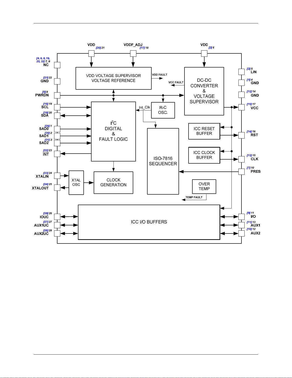
FUNCTIONAL DIAGRAM
Figure 1: 73S8010C Block Diagram
Pin number reference to SO28 Package
[Pin number] reference to 32QFN Package
2 Rev. 1.5

DS_8010C_024 73S8010C Data Sheet
Table of Contents
1 Pin Description .................................................................................................................................... 5
1.1 Card Interface ............................................................................................................................... 5
1.2 Miscellaneous Inputs and Outputs ................................................................................................ 5
1.3 Power Supply and Ground ............................................................................................................ 5
1.4 Microcontroller Interface ............................................................................................................... 6
2 Host Interface (I2C Bus) ...................................................................................................................... 7
2.1 Host Interface Control ................................................................................................................... 7
2.2 Host Interface Status .................................................................................................................... 8
2.3 I2C-bus Timing .............................................................................................................................. 9
3 Oscillator ............................................................................................................................................ 10
4 DC-DC Converter – Card Power Supply ......................................................................................... 10
5 Voltage Supervision ......................................................................................................................... 11
6 Power Down ....................................................................................................................................... 11
7 Over-temperature Monitor ................................................................................................................ 12
8 Activation Sequence ......................................................................................................................... 12
9 Deactivation Sequence ..................................................................................................................... 13
10 Interrupt ............................................................................................................................................. 13
11 Warm Reset .................................................................................................................... ................... 14
12 I/O Timing ........................................................................................................................................... 14
13 Typical Application Schematic ........................................................................................................ 15
14 Electrical Specification ..................................................................................................................... 16
14.1Absolute Maximum Ratings ........................................................................................................ 16
14.2Recommended Operating Conditions......................................................................................... 16
14.3DC Characteristics: Card Interface ............................................................................................. 17
14.4DC Characteristics: Digital Signals ............................................................................................. 20
14.5DC Characteristics: Supply ......................................................................................................... 20
14.6DC Characteristics: I2C Interface ................................................................................................ 21
14.7Voltage / Temperature Fault Detection Circuits .......................................................................... 21
15 Mechanical Drawings ....................................................................................................................... 22
15.132-pin QFN ................................................................................................................................. 22
15.228-pin SO .................................................................................................................................... 23
16 Package Pin Designation ................................................................................................................. 24
16.132-pin QFN ................................................................................................................................. 24
16.228-pin SO .................................................................................................................................... 25
17 Ordering Information ........................................................................................................................ 26
18 Related Documentation .................................................................................................................... 26
19 Contact Information .......................................................................................................................... 26
Revision History ........................................................................................................................................ 27
Rev. 1.5 3

73S8010C Data Sheet DS_8010C_024
Figures
Figure 1: 73S8010C Block Diagram ............................................................................................................. 2
Figure 2: I2C Bus Write Protocol ................................................................................................................... 8
Figure 3: I2C Bus Read Protocol ................................................................................................................... 9
Figure 4: I2C Bus Timing Diagram ................................................................................................................ 9
Figure 5: Power Down Mode Operation ...................................................................................................... 12
Figure 6: Activation Sequence .................................................................................................................... 12
Figure 7: Deactivation Sequence ................................................................................................................ 13
Figure 8: FAULT Functions, INT operation ................................................................................................. 13
Figure 9: Warm Reset operation ................................................................................................................. 14
Figure 10: I/O Timing .................................................................................................................................. 14
Figure 11: 73S8010C – Typical Application Schematic .............................................................................. 15
Figure 12: DC – DC Converter Efficiency (VCC = 5 V) ................................................................................ 18
Figure 13: DC – DC Converter Efficiency (VCC = 3 V) ................................................................................ 18
Figure 14: 32-pin QFN Package Drawing ................................................................................................... 22
Figure 15: 28-pin SO Package Drawing ..................................................................................................... 23
Tables
Table 1: Device Address Selections ............................................................................................................. 7
Table 2: Host Control Register ...................................................................................................................... 7
Table 3: Host Status Register ....................................................................................................................... 8
Table 4: Choice of Vcc Capacitor ............................................................................................................... 10
4 Rev. 1.5
DS_8010C_024 73S8010C Data Sheet
1 Pin Description
1.1 Card Interface
Name
Pin
(SO)
I/O 11 9 Card I/O: Data signal to/from card. Includes a pull-up resistor to V
PIN
(QFN)
Description
CC.
AUX1 13 11 AUX1: Auxiliary data signal to/from card. Includes a pull-up resistor to V
AUX2 12 10 AUX2: Auxiliary data signal to/from card. Includes a pull-up resistor to V
RST 16 14 Card reset: provides reset (RST) signal to card.
CLK 15 13
Card clock: provides clock (CLK) signal to card. The rate of this clock is
determined by the crystal oscillator frequency and CLKSEL bits in the
control register.
PRES 10 7
Card Presence switch: active high indicates card is present. Includes a
pull-down resistor.
VCC 17 15
Card power supply: logically controlled by sequencer, output of DC-DC
converter. Requires an external filter capacitor to the card GND.
GND 14 12 Card ground.
1.2 Miscellaneous Inputs and Outputs
Name
PIN
(SO)
XTALIN 24 23
XTALOUT 25 24
VDDF_ADJ 18 17
NC 7, 9
PIN
(QFN)
4, 6, 8,
16, 25,
32
Description
Crystal oscillator input: can either be connected to a crystal or driven
as a source for the card clock.
Crystal oscillator output: connected to crystal. Left open if XTALIN is
being used as an external clock input.
V
threshold adjustment input: this pin can be used to overwrite a
DD
higher V
value (that controls deactivation of the card). Must be
DDF
left open if unused.
Non-connected pin.
1.3 Power Supply and Ground
CC.
CC.
Name
PIN
(SO)
VDD 6, 21 3, 20
Pin
(QFN)
Description
System controller interface supply voltage: supply voltage for internal
circuitry and DC-DC converter power supply source.
GND 4 1 DC-DC converter ground.
GND 14 12 Smart Card I/O ground.
GND 22 21 Digital ground.
LIN 5 2
External inductor: Connect external inductor from pin 5 to V
. Keep the
DD
inductor close to pin 5.
Rev. 1.5 5
73S8010C Data Sheet DS_8010C_024
1.4 Microcontroller Interface
Name
PIN
(SO)
INT 23 22
PWRDN 8 5
PIN
(QFN)
Description
Interrupt output (negative assertion): Interrupt output signal to the
processor. A 20 kΩ pull up to V
DD
Power Down control input: Active High. When Power Down (PD) mode is
activated, all internal analog functions are disabled to place the 73S8010C
in its lowest power consumption mode. Must be tied to ground when the
power down function is not used.
SAD0
SAD1
SAD2
1
2
3
Serial device address bits: Digital inputs for address selection that allow
29
the connection of up to 8 devices in parallel. Address selections as follows:
30
31
SAD2 SAD1 SAD0 I
0 0 0 0x40
0 0 1 0x42
0 1 0 0x44
0 1 1 0x46
1 0 0 0x48
1 0 1 0x4A
1 1 0 0x4C
1 1 1 0x4E
Pins SAD0 and SAD1 are internally pulled-down and SAD2 is
internally pulled-up.
The default address when left unconnected is 48h.
SCL 19 18 I2C clock signal input.
SDA 20 19 I2C bi-directional serial data signal.
I/OUC 26 26
AUX1UC 27 27
AUX2UC 28 28
System controller data I/O to/from the card. Includes internal pull-up
resistor to V
DD.
System controller auxiliary data I/O to/from the card. Includes internal pullup resistor to V
DD.
System controller auxiliary data I/O to/from the card. Includes internal pullup resistor to V
DD.
is provided internally.
2
C Address (7 bits)
6 Rev. 1.5
DS_8010C_024 73S8010C Data Sheet
2 Host Interface (I2C Bus)
A fast-mode 400 kHz I2C bus slave interface is used for controlling the device and reading the status of
the device via the data pin SDA and clock pin SCL. The bus has 3 address select pins, SAD0, SAD1,
and SAD2. This allows up to 8 devices to be connected in parallel.
Table 1: Device Address Selections
SAD2 SAD1 SAD0 I
0 0 0 0x40
0 0 1 0x42
0 1 0 0x44
0 1 1 0x46
1 0 0 0x48
1 0 1 0x4A
1 1 0 0x4C
1 1 1 0x4E
Bit 0 of the I
2
C address is the R/W bit. Refer to Figure 2 and Figure 3 for usage.
2.1 Host Interface Control
2
C Address (7 bits)
Table 2 describes the Host Interface Control Register bits (power-on Reset = 0x00).
Table 2: Host Control Register
Name Bit Description
Start/Stop 0
When set, initiates an activation and a cold reset procedure; when reset, initiates
a deactivation sequence.
Warm reset 1
When set, initiates a warm reset procedure; automatically reset by hardware
when the card starts answering or when the card is declared mute.
5 V and 3 V 2 When set, VCC = 3 V; when reset, VCC = 5 V.
Clock Stop 3 When set, card clock is stopped. Bit 4 determines the card clock stop level.
Clock Stop
4 When set, card clock stops high; when reset card clock stops low.
Level
Clksel1 5
Bits 5 and 6 determine the clock rate to the card according to the following table.
CLKDIV1 CLKDIV2 Clock Rate
Clksel2 6
0 0 XTALIN/8
0 1 XTALIN/4
1 1 XTALIN/2
1 0 XTALIN
I/O enable 7
When set, data is transferred between I/O (AUX1, AUX2) and I/OUC (AUX1UC,
AUX2UC); when reset, I/O (AUX1, AUX2) and I/OUC (AUX1UC, AUX2UC) are
high impedance.
2
C-bus Write to the Control Register
I
2
The I
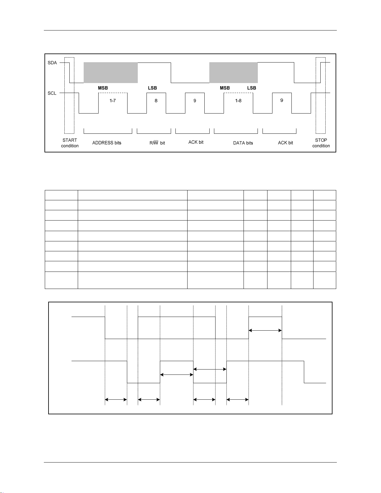
C-bus Write command to the control register follows the format shown in Figure 2.
After the START condition, the master sends a slave address. This address is seven bits long followed
by an eighth bit, which is an opcode bit (R/W) – a ‘zero’ indicates the master will write data to the control
register. After the R/W bit, the ’zero’ ACK bit is sent to the master by the device. The master now starts
sending the 8 bits of data to the control register during the DATA bits time. After the DATA bits, the ‘zero’
Rev. 1.5 7

73S8010C Data Sheet DS_8010C_024
ACK bit is sent to the master by the device. The master should send the STOP condition after receiving
the ACK bit.
Figure 2: I
2
C Bus Write Protocol
2.2 Host Interface Status
Table 3 describes the Host Interface Status Register bits (power-on Reset = 0x04).
Table 3: Host Status Register
Name Bit Description
PRES 0 Set when the card is present; reset when the card is not present.
PRESL 1
I/O 2 Set when I/O is high; reset when I/O is low.
SUPL 3
PROT 4
MUTE 5
EARLY 6
ACTIVE 7 Set when the card is active (VCC is on); reset when the card is inactive.
2
I
C-bus Read from the Status Register:
2
The I
C-bus Read Command from the Status Register follows the format shown in Figure 3.
After the START condition, the master sends a slave address. This address is seven bits long followed
by an eighth bit, which is the opcode bit (R/W). A ‘one’ indicates the master will read data from the status
register. After the R/W bit, the ’zero’ ACK bit is sent to the master by the device. The device now starts
sending the 8-bit status register data to the control register during the DATA bits time. After the DATA
bits, the ‘one’ ACK bit is sent to the device by the master. The master should send the STOP condition
after receiving the ACK bit.
Set when the PRES pin changes state (rising/falling edge); reset when the status
register is read. Generates an interrupt when set
Set when a voltage fault is detected; reset when the status register is read.
Generates an interrupt when set.
Set when an over-current or over-heating fault has occurred during a card session;
reset when the status register is read. Generates an interrupt when set.
Set during ATR when the card has not answered during the ISO 7816-3 time
window (40000 card clock cycles); reset when the next session begins or this
register is read.
Set during ATR when the card has answered before 400 card clock cycles; reset
when the next session begins or this register is read.
8 Rev. 1.5
DS_8010C_024 73S8010C Data Sheet
Figure 3: I
2
C Bus Read Protocol
2.3 I2C-bus Timing
Symbol Parameter Conditions Min. Typ. Max. UNIT
Fsclk Clock frequency 400 kHz
Tlow Clock low 1.3
Thi Clock high 0.6
Thdsta Hold time START condition 0.6
Tsudat Data set up time 100 ns
Thddat Data hold time 5 900 ns
Tsusto Set up time STOP condition 0.6
Tbuf
Bus free time between a STOP and
1.3
START condition
SDA
Tbuf
s
s
s
s
s
SCL
Tlow
Thi
Thdsta
Tsudat Thddat Tsusto
Figure 4: I
2
C Bus Timing Diagram
Rev. 1.5 9

73S8010C Data Sheet DS_8010C_024
3 Oscillator
The Teridian 73S8010C device has an on-chip oscillator that can generate the smart card clock using an
external crystal, connected between the XTALIN and XTALOUT pins, to set the oscillator frequency.
When the card clock signal is available from another source, it can be connected to the pin XTALIN, and
the pin XTALOUT should be left unconnected.
4 DC-DC Converter – Card Power Supply
An internal DC-DC converter provides the card power supply. This converter is able to provide either a
3 V or 5 V card voltage from the power supply applied on the V
controls the converter. Bit 2 of the Control register selects the card voltage.
The circuit is an inductive step-up converter/regulator. The external components required are 2 filter
capacitors on the power-supply input V
filter capacitor on the card power supply V
operation when V
input supply V
3.6 V, V
= 3 V) the circuit operates as a linear regulator. Depending on the inductor values, the voltage
CC
is below a set point of 5.0 or 3.0 volts minus a comparator hysteresis voltage and the
CC
is less than the set point for VCC. When VDD is greater than the set point for VCC (VDD =
DD
converter can provide current on V
(100 nF + 10 F, next to the LIN pin), an inductor, and an output
DD
. The circuit performs regulation by activating the step-up
CC
as high as 100 mA.
CC
The circuit provides over-current protection and limits I
to 150 mA. When an over-current condition is
CC
sensed, the circuit initiates a deactivation sequence from the control logic and reports back to the host
controller a fault on the interrupt output INT.
Choice of the Inductor
The nominal inductor value is 10 H, rated for 400 mA. The inductor is connected between pin LIN (pin 5
in the SO package, pin 2 in the QFN package) and the V
optimized to meet a particular configuration (I
CC_MAX
DD
). The inductor should be located on the PCB as
close as possible to the LIN pin of the IC.
Choice of the V
Capacitor
CC
Depending on the applications, the requirements in terms of both V
currents that the interface must be able to provide to the card vary. Table 4 shows the recommended
capacitors for each V
power supply configuration and applicable specification.
CC
pin. The digital ISO-7816-3 sequencer
DD
voltage. The value of the inductor can be
minimum voltage and transient
CC
Table 4: Choice of Vcc Capacitor
Specification Requirement Application
Min V
Specification
Allowed During
Transient Current
EMV 4.0 4.6V 30nA.s
ISO-7816-3 4.5V 20nA.s
Voltage
CC
Max Transient
Current Charge
Capacitor Type Capacitor Value
X5R/X7R w/
ESR < 100 m
3.3 F
1 F
10 Rev. 1.5

DS_8010C_024 73S8010C Data Sheet
5 Voltage Supervision
Two voltage supervisors constantly check the level of the VDD and V
voltages. A card deactivation
CC
sequence is forced when a fault occurs for any of these voltage supervisors.
The digital circuitry is powered by the power supply applied on the VDD pin. V
range to interface with the system controller. The V
voltage supervisor is also used to initialize the
DD
also defines the voltage
DD
ISO-7816-3 sequencer at power-on, and to deactivate the card at power-off or when a fault occurs. The
voltage threshold of the V
voltage supervisor is internally set by default to 2.3 V nominal. However, it
DD
may be desirable in some applications, to modify this threshold value. The pin VDDF_ADJ (pin 18 in the
SO package, pin 17 in the QFN package) is used to connect an external resistor R
the V
fault voltage to another value, V
DD
R
= 180 kΩ / (V
EXT
- 2.33)
DDF
(refer to Figure 11). The resistor value is defined as follows:
DDF
to ground to raise
EXT1
An alternative (more accurate) method of adjusting the VDD fault voltage is to use a resistive network of
R3 from the pin to supply and R4 from the pin to ground (see Figure 11). In order to set the new
threshold voltage, the equivalent resistance must be determined. This resistance value will be
designated Kx. Kx is defined as R4/(R4+R5). Kx is calculated as:
Kx = (2.649 / VTH) - 0.6042 where VTH is the desired new threshold voltage.
To determine the values of R4 and R5, use the following formulas.
R5 = 72000 / Kx R4 = R5*(Kx / (1 – Kx))
Taking the example above, where a VDD fault threshold voltage of 2.7 V is desired, solving for Kx gives:
Kx = (2.649 / 2.7) - 0.6042 = 0.377.
Solving for R5 gives: R5 = 72000 / 0.377 = 191 k.
Solving for R4 gives: R4 = 191000 *(0.377 / (1 – 0.377)) = 115.6 k.
Using standard 1% resistor values gives R5 = 191 kand R4 = 115 kThese values give an equivalent
resistance of Kx = 0.376, a 0.3% error.
If the 2.3 V default threshold is used, the VDDF_ADJ pin must be left unconnected.
6 Power Down
A power down function is provided via the PWRDN pin (active high). When activated, the Power Down
(PD) mode disables all the internal analog functions, including the card analog interface, the oscillators
and the DC-DC converter, to put the 73S8010C in its lowest power consumption mode. PD mode is only
allowed in the deactivated condition (out of a card session, when the Start/Stop bit is set to 0 from the I
2
C
host controller).
The host controller invokes the power down state when it is desirable to save power. The signal PRES
remains functional in PD mode such that a card insertion sets INT high. The micro-controller must then
set PWRDN low and wait for the internal stabilization time prior to starting any card session (prior to
setting the Start/Stop bit to 1).
Resumption of the normal mode occurs approximately 10 ms (stabilization of the internal oscillators +
reset of the circuitry) after PWRDN is set low. No card activation should be invoked during this 10 ms
time period. If a card is present, INT can be used as an indication that the circuit has completed its
recovery from power down state. INT will go high at the end of the stabilization period. Should the
Start/Stop be set to 1 during PWRDN = 1, or within the 10 ms internal stabilization / reset time, it will not
be taken into account and the card interface will remain inactive. Since Start/Stop is taken into account
on its edges, it should be toggled low and high again after the 10 ms to activate a card.
Figure 5 illustrates the sequencing of the PD and Normal modes. PWRDN must be connected to GND if
the power down function is not used.
Rev. 1.5 11

73S8010C Data Sheet DS_8010C_024
PRES
INT
PWRDN during a card
PWRDN
OFF follows PRES regardless of PWRDN
session has no effect
PWRDN has effect when
the cardi s deactivated
Internal RC OSC
~10ms
Start/Stop bit
After setting PWRDN = 0,
the controller must wait at
least 10ms before setting
Start/Stop = 1
EMV / ISO deactivation
time ~= 100 uS
Figure 5: Power Down Mode Operation
7 Over-temperature Monitor
A built-in detector monitors die temperature. When an over-temperature condition occurs (most likely
resulting from a heavily loaded card interface, including short circuits), a card deactivation sequence is
initiated, and a fault condition is reported to the system controller (bit 4 of the status register is set and
generates an interrupt).
8 Activation Sequence
After Power on Reset, the INT signal is low until VDD is stable. When VDD has been stable for
approximately 10 ms and the INT signal is high, the system controller may read the status register to see
if the card is present. If all the status bits are satisfactory, the system controller can initiate the activation
sequence by writing a ‘1’ to the Start/Stop bit (bit 0 of the Control register).
The following steps and Figure 6 show the activation sequence and the timing of the card control signals
when the system controller initiates the Start/Stop bit (bit 0) of the control register:
1. Voltage VCC to the card should be valid by the end of t1. If VCC is not valid for any reason, then the
session is aborted.
2. Turn I/O to reception mode at the end of t
3. CLK is applied to the card at the end of t
4. RST (to the card) is set high at the end of t
.
1
.
2
.
3
t1 = 0.510 ms (timing by 1.5 MHz internal Oscillator), I/O in reception mode
≥ 0.5 μs, CLK starts
t
2
t
≥ 42000 card clock cycles, RST set high
3
Figure 6: Activation Sequence
12 Rev. 1.5

DS_8010C_024 73S8010C Data Sheet
9 Deactivation Sequence
Deactivation is initiated either by the system controller resetting the Start/Stop bit, or automatically in the
event of hardware faults. Hardware faults are over-current, over-temperature, V
card extraction during the session.
The following steps and Figure 7 show the deactivation sequence and the timing of the card control
signals when the system controller clears the Start/Stop bit:
1. RST goes low at the end of t
2. CLK goes low at the end of t
3. I/O goes low at the end of t
4. Shut down V
at the end of time t4.
CC
.
1
.
2
. Out of reception mode.
3
fault, VCC fault, and
DD
t1 ≥ 0.5 μs t3 ≥ 0.5 μs
t
≥ 7.5 μs t4 ≥ 0.5 μs
2
Figure 7: Deactivation Sequence
10 Interrupt
The interrupt is an active low interrupt. It is set low if either a VCC fault or a VDD fault is detected. It is also
set low if one of the following status bit conditions is detected:
Early ATR
Mute ATR
Card insert or card extract
Protection status from Over-current or Over-heating
If the interrupt is set low by the detection of these status bits, then the interrupt is set high when these
status bits are read. (READ STATUS DONE)
INT
ANY FAULT
STATUS BITS
READ STATUS DONE
Figure 8: FAULT Functions, INT operation
Rev. 1.5 13

73S8010C Data Sheet DS_8010C_024
A power-on-reset (POR) event will reset all of the control and status registers to their default states. A VDD fault
event does not reset these registers, but it will signal an interrupt condition and by the action of the timer that
creates interval “t
considered valid for V
,” will not clear the interrupt until VDD is valid for at least the t1 time. The VDD fault can be
1
as low as 1.5 to 1.8 volts. At the lower range of the VDD fault, POR will be asserted.
DD
11 Warm Reset
The 73S8010C automatically asserts a warm reset to the card when instructed through bit 1 of the I2C Control
register (Warm Reset bit). The warm reset length is automatically defined as 42,000 card clock cycles. The bit
Warm Reset is automatically reset when the card starts answering or when the card is declared mute.
IO
Warm Reset
(bit 1)
RST
t
1
t
2
t
3
t1> 1.5 µs, Warm Reset Starts
t2= 42000 card clock cycles, End of Warm Reset
t3= Resets Warm Reset bit 1 when detected ATR or Mute
Figure 9: Warm Reset operation
12 I/O Timing
The states of the I/O, AUX1, and AUX2 pins are low after power on reset and they are high when the
activation sequencer turns on the I/O reception state. See Section 8 Activation Sequence for more
details on when the I/O reception is enabled.
The states of I/OUC, AUX1UC, and AUX2UC are high after power on reset. When the control I/O enable
bit (bit 7 of the Control register) is set, the first I/O line on which a falling edge is detected becomes the
input I/O line and the other becomes the output I/O line. When the input I/O line rising edge is detected
then both I/O lines return to their neutral state. The delay between the I/O signals is shown in Figure 10.
Delay from I/O to I/OUC: t
Delay from I/OUC to I/O: t
= 100 ns t
IO_HL
I/OUC_HL
= 100 ns t
= 25 ns
IO_LH
I/OUC_LH
= 25 ns
Figure 10: I/O Timing
14 Rev. 1.5

DS_8010C_024 73S8010C Data Sheet
13 Typical Application Schematic
SAD0
SAD1
SAD2
GND
GND
VPC
NC
NC
NC
PRES
I/O
AUX2
AUX1
GND
Card detection
swit ch is normally
closed.
VDD
AUX2UC
AUX1UC
I/OUC
XTA L OU T
XTA L I N
VDD_AD J
10
SW-19SW-2
Smart C ard Connec tor
INT_
GND
VDD
SDA
SCL
VCC
RST
CLK
SO28
8
R5
Rext2
28
27
26
25
24
23
22
21
20
19
18
17
16
15
5
3
6
4
7
C8
2
C4
I/O
CLK
VPP
GND
R4
Rext1
See
note 6
ISO7816=1uF, EMV=3.3uF
Low ESR (< 1 0 0 mohms) C1
should be placed near the SC
C1
connecter contact
CLK tra ck sho uld be route d
far from RST, I/O, C4 and
1
C8.
RST
VCC
See NOTE 1
C6
100nF
R3 2K
R2 2K
SAD0
SAD1
SAD2
Note 2
C4
100nF
C5
10uF
L1 10uH
See note 7
PWRD N_f rom_uC
See NOTE 5
1
2
3
4
5
6
7
8
9
10
11
12
13
14
73S8010C
NOTES:
1) VDD supply should be = 2.7V to 3.6V DC.
2) Hardwire to define address of device
3) Required if external clock from uP is used.
4) Required if crystal is used.
Y1, C2 and C3 must be removed if external clock is used.
5) Pin can not float. Must be driven or connected to GND
if power down function is not used.
6) Rext1 and Rext2 are external resistors to ground and
VDD to modify the VDD fault voltage. Can be left open
7) Keep L1 cl ose to pi n 5
VDD
R1
20K
AUX2UC_to/ from _uC
AUX1UC_to. from _uC
IOUC _to/f rom_uC
INT_interrupt _to_uC
SDA_f rom_uC
SCL_f rom_uC
Figure 11: 73S8010C – Typical Application Schematic
See NOTE 5
See NOTE 3
External_c lock _f rom uC
- OR -
C2
Y1
C3
CRYSTAL
See NOTE 4
22pF
22pF
Rev. 1.5 15

73S8010C Data Sheet DS_8010C_024
14 Electrical Specification
14.1 Absolute Maximum Ratings
Operation outside these rating limits may cause permanent damage to the device.
Parameter Rating
Supply Voltage VDD -0.5 to 4.0 VDC
Input Voltage for Digital Inputs -0.3 to (VDD +0.5) VDC
Storage Temperature -60 °C to 150 °C
Pin Voltage (except LIN and card interface) -0.3 to (VDD +0.5) VDC
Pin Voltage (LIN) -0.3 to 6.0 VDC
Pin Voltage (card interface) -0.3 to (VCC + 0.5) VDC
ESD Tolerance – Card interface pins +/- 6 kV
ESD Tolerance – Other pins +/- 2 kV
ESD testing on Card pins uses the HBM condition, 3 pulses, each polarity referenced to ground.
14.2 Recommended Operating Conditions
Parameter Rating
Supply Voltage VDD 2.7 to 3.6 VDC
Ambient Operating Temperature -40 °C to +85 °C
Input Voltage for Digital Inputs 0 V to VDD + 0.3 V
16 Rev. 1.5

DS_8010C_024 73S8010C Data Sheet
14.3 DC Characteristics: Card Interface
Symbol Parameter Condition Min. Typ. Max. Unit
Card Power Supply (VCC) DC-DC Converter
General conditions, -40 C < T < 85 C, 2.7 V < V
Inactive mode -0.1 0.1 V
Inactive mode
Active mode
I
CC
Active mode
I
CC
Active mode
single pulse of 100 mA
for 2 s; 5 V,
VCC
Card supply voltage
including ripple and noise
fixed load = 25 mA
Active mode
single pulse of 100 mA
for 2 s; 3 V,
fixed load = 25 mA
Active mode
current pulses of 40 nAs
with peak |I
t < 400 ns; 5 V
Active mode
current pulses of 40 nAs
with peak |I
t < 400 ns; 3 V
Static load current,
V
> 4.6 or 2.7 V as
CC
selected, L=10 H
on VCC = 1 µF 0.05 0.15 0.25
C
F
on VCC = 1 µF 0.1 0.3 0.5
C
F
I
CCmax
I
I
CCF
VSR
VSF
CF
Maximum supply current to
the card
fault current Short circuit, VCC to ground 100 125 180 mA
CC
V
slew rate - Rise rate on
CC
activate
V
slew rate - Fall rate on
CC
deactivate
External filter capacitor
(V
to GND)
CC
L Inductor (LIN to VDD) 10
V
= 5 V, I
Limax Imax in inductor
Efficiency
CC
V
CC
V
= 5 V, I
V
< 3.6 V
DD
I
= 1 mA
CC
< 65 mA; 5 V
< 65 mA; 3 V
-0.1 0.4 V
4.75 5.25 V
2.8 3.2 V
4.6 5.25 V
2.76 3.2 V
| < 200 mA,
CC
| < 200 mA,
CC
4.6 5.25 V
2.76 3.2 V
mA
100
0.47 1 3.3
= 65 mA,
CC
= 2.7 V
DD
CC
= 3.3 V
DD
= 65 mA,
400 mA
87 %
V/s
V/s
F
H
Rev. 1.5 17

73S8010C Data Sheet DS_8010C_024
1011B01 Converter efficiency (VCC 5V)
Converter Efficiency (V
100
95
90
85
80
75
CC
5 V)
70
Efficiency [%]
65
60
55
50
0 20406080100
2.7V
3.0V
3.3V
3.6V
Icc [mA]
Figure 12: DC – DC Converter Efficiency (V
Output current on Vcc at 5 V. Input voltage on V
1011B01 Converter efficiency (VCC 3V)
100
95
90
85
= 5 V)
CC
at 2.7, 3.0, 3.3 and 3.6 volts.
DD
80
75
70
Efficiency [%]
65
60
55
50
0 20 40 60 80 100
2.7V
3.0V
3.3V (Linear)
3.6V (Linear)
Icc [mA]
Figure 13: DC – DC Converter Efficiency (VCC = 3 V)
Output current on V
18 Rev. 1.5
at 3 V. Input voltage on VDD at 2.7, 3.0, 3.3 and 3.6 volts.
CC

DS_8010C_024 73S8010C Data Sheet
Symbol Parameter Condition Min. Typ. Max. Unit
Interface Requirements – Data Signals: I/O, AUX1, AUX2, and host interfaces: I/OUC, AUX1UC,
AUX2UC. I
SHORTL
, I
SHORTH
, and V
requirements do not pertain to I/OUC, AUX1UC, and AUX2UC. IIL
INACT
requirements only pertain to I//OUC, AUX1UC, and AUX2UC.
= 0 0.9 VCC VCC+ 0.1 V
I
VOH
VOH
Output level, high (I/O, AUX1,
AUX2)
Output level, high (I/OUC,
AUX1UC, AUX2UC)
OH
IOH = -40 A
= 0 0.9 VDD VDD+ 0.1 V
I
OH
IOH = -40 A
0.75 V
0.75 V
CC
DD
VCC + 0.1 V
VDD + 0.1 V
VOL Output level, low IOL=1 mA 0.3 V
VIH
VIH
Input level, high (I/O, AUX1,
AUX2)
Input level, high (I/OUC,
AUX1UC, AUX2UC)
1.8 V
+ 0.30 V
CC
1.8 VDD + 0.30 V
VIL Input level, low -0.3 0.8 V
I
= 0 0.1 V
V
I
LEAK
INACT
Output voltage when outside
of session
Input leakage VIH = VCC 10
IIL Input current, low
I
Short circuit output current
SHORTL
I
Short circuit output current
SHORTH
For output low, shorted
to V
For output high, shorted
to ground through 33
OL
IOL = 1 mA 0.3 V
A
V
= 0, CS = 1 0.65 mA
IL
VIL = 0, CS = 0 5 μA
through 33
CC
15 mA
15 mA
For I/O, AUX1, AUX2,
C
= 80 pF, 10% to 90%
L
tR, tF Output rise time, fall times
For I/OUC, AUX1UC,
100 ns
AUX2UC,
CL=50 pF, 10% to 90%
tIR, tIF Input rise, fall times
RPU Internal pull-up resistor Output stable for >200 ns 8 11 14
FD
Maximum data rate 1
MAX
T
FDIO
Delay, I/O to I/OUC,
I/OUC to I/O
1
s
k
MHz
20 ns
CIN Input capacitance 10 pF
Rev. 1.5 19

73S8010C Data Sheet DS_8010C_024
Symbol Parameter Condition Min. Typ. Max. Unit
Reset and Clock for card interface, RST, CLK
VOH Output level, high
VOL Output level, low
V
INACT
I
RST_LIM
I
CLK_LIM
Output voltage when outside of
a session
Output current limit, RST 30 mA
Output current limit, CLK 70 mA
tR, tF Output rise time, fall time
I
= -200 A
OH
I
= 200 A
OL
I
= 0 0.1 V
OL
IOL = 1 mA 0.3 V
= 35 pF for CLK,
C
L
10% to 90%
CL = 200 pF for RST,
0.9 V
10% to 90%
C
Duty cycle for CLK,
except for f=f
XTAL
=35 pF,
L
20 MHz
F
CLK
VCC V
CC
0 0.3 V
8 ns
100 ns
45 55 %
14.4 DC Characteristics: Digital Signals
Symbol Parameter Condition Min. Typ. Max. Unit
Digital I/O except for OSC I/O
VIL Input Low Voltage -0.3 0.8 V
VIH Input High Voltage 1.8 VDD + 0.3 V
VOL Output Low Voltage IOL = 2 mA 0.45 V
VOH Output High Voltage IOH = -1 mA VDD - 0.45 V
R
Pull-up resistor, INT 20
OUT
|I
| Input Leakage Current GND < VIN < VDD -5 5 μA
IL1
Oscillator (XTALIN) I/O Parameters
V
Input Low Voltage - XTALIN -0.3 0.3 VDD V
ILXTAL
V
Input High Voltage - XTALIN 0.7 VDD VDD+0.3 V
IHXTAL
I
Input Current - XTALIN GND < VIN < VDD -30 30 μA
ILXTAL
f
Max freq. Osc or external clock 27 MHz
MAX
t
in
External input duty cycle limit
R/F < 10% fIN,
45% <
CLK
< 55%
48 52 %
k
14.5 DC Characteristics: Supply
Symbol Parameter Condition Min. Typ. Max. Unit
Linear mode, ICC=0
IDD Supply Current on VDD
I/O, AUX1, AUX2=high
Step up mode, ICC=0
I/O, AUX1, AUX2=high
PWRDN=1, Start/stop bit = 0
DD
All digital inputs driven with a
true logical 0 or 1
I
DD_PD
Supply Current on V
in Power Down mode
20 Rev. 1.5
4.9 mA
4.7 mA
0.11 2.5
A

DS_8010C_024 73S8010C Data Sheet
14.6 DC Characteristics: I2C Interface
Symbol Parameter Condition Min. Typ. Max. Unit
SDA, SCL
VIL Input Low Voltage -0.3 0.3* VDD V
VIH Input High Voltage 0.7*VDD VDD + 0.3 V
VOL Output Low Voltage IOL = 3 mA 0.40 V
CIN Pin capacitance 10 pF
IIN Output High Voltage IOH = -1 mA VDD - 0.45 V
TF Output fall time CL = 0 to 400 pF
TSP
Pulse width of spikes
that are suppressed
Transition from valid logic
level to opposite level
20 + 0.1*C
250 ns
L
50 ns
14.7 Voltage / Temperature Fault Detection Circuits
Symbol Parameter Condition Min. Typ. Max. Unit
fault – VDD Voltage
V
V
DDF
V
CCF
DD
supervisor threshold
fault – VCC Voltage
V
CC
supervisor threshold
TF Die over temperature fault 115 145
No external resistor on
VDDF_ADJ pin
= 5 V 4.20 4.6 V
V
CC
VCC= 3 V 2.5 2.7 V
2.15 2.4 V
C
Rev. 1.5 21

73S8010C Data Sheet DS_8010C_024
15 Mechanical Drawings
15.1 32-pin QFN
0.85 NOM ./ 0.9MAX.
5
2.5
1
2
3
TOP VIEW
0.35 / 0.45
2.5
0.18 / 0.3
5
3.0 / 3.75
1.5 / 1.875
SIDE VIEW
CHAMFERED
0.30
0.00 / 0.005
0.20 REF.
SEATING
PLANE
1
2
3
0.25
0.5
0.2 MIN.
0.35 / 0.45
0.25
0.5
3.0 / 3.75
1.5 / 1.875
BOTTOM VIEW
Figure 14: 32-pin QFN Package Drawing
22 Rev. 1.5

DS_8010C_024 73S8010C Data Sheet
15.2 28-pin SO
Figure 15: 28-pin SO Package Drawing
Rev. 1.5 23

73S8010C Data Sheet DS_8010C_024
16 Package Pin Designation
Use handling procedures necessary for a static sensitive component.
16.1 32-pin QFN
GND
LIN
VDD
NC
PRDWN
NC
PRES
SAD2
NC
31
32
1
2
3
4
5
6
7
8
9
I/O
73S8010C
10
AUX2
SAD0
SAD1
30
29
AUX2UC
28
TERIDIAN
11
12
13
CLK
GND
AUX1
AUX1UC
27
14
RST
I/OUC
26
15
VCC
NC
25
24
23
22
21
20
19
18
17
16
NC
Figure 13: 73S8010C 32-pin QFN Pin Out
(Top View)
XTALOUT
XTALIN
INT
GND
VDD
SDA
SCL
VDDF_ADJNC
24 Rev. 1.5

DS_8010C_024 73S8010C Data Sheet
16.2 28-pin SO
SAD0
1
SAD1
SAD2
GND
LIN
2
3
4
5
VDD
6
NC
PWRDN
NC
PRES
I/O
7
73S8010C
8
9
10
11
AUX2
12
AUX1
GND
13
14
Figure 15: 73S8010C 28-pin SO Pin Out
(Top View)
28
27
26
25
24
23
22
20
19
18
17
16
15
21
AUX2UC
AUX1UC
I/OU C
XTALOUT
XTALIN
INT
GND
VDD
SDA
SCL
VDDF_ADJ
VCC
RST
CLK
Rev. 1.5 25

73S8010C Data Sheet DS_8010C_024
17 Ordering Information
Part Description Order Number Packaging Mark
73S8010C-SO 28-pin Lead-Free SO 73S8010C-IL/F 73S8010C-IL
73S8010C-SO 28-pin Lead-Free SO Tape / Reel 73S8010C-ILR/F 73S8010C-IL
73S8010C-QFN 32-pin Lead-Free QFN 73S8010C-IM/F 73S8010C
73S8010C-QFN 32-pin Lead-Free QFN Tape / Reel 73S8010C-IMR/F 73S8010C
18 Related Documentation
The following 73S8010C documents are available from Teridian Semiconductor Corporation:
73S8010C Data Sheet (this document)
73S8010C 28SO Demo Board User’s Guide
73S8010C QFN Demo Board User’s Guide
19 Contact Information
For more information about Teridian Semiconductor products or to check the availability of the
73S8010C, contact us at:
6440 Oak Canyon Road
Suite 100
Irvine, CA 92618-5201
Telephone: (714) 508-8800
FAX: (714) 508-8878
Email: scr.support@teridian.com
For a complete list of worldwide sales offices, go to http://www.teridian.com.
26 Rev. 1.5

DS_8010C_024 73S8010C Data Sheet
Revision History
Revision Date Description
1.0 6/13/2005 First publication.
1.2 9/21/2005 Changed SDATA hold time.
1.3 12/5/2007
1.4 1/17/2008 Changed dimension of bottom exposed pad on 32QFN mechanical package
1.5 4/3/2009 Removed all references to VPC as VPC must be tied to VDD.
© 2009 Teridian Semiconductor Corporation. All rights reserved.
Teridian Semiconductor Corporation is a registered trademark of Teridian Semiconductor Corporation.
Simplifying System Integration is a trademark of Teridian Semiconductor Corporation.
All other trademarks are the property of their respective owners.
Teridian Semiconductor Corporation makes no warranty for the use of its products, other than expressly
contained in the Company’s warranty detailed in the Teridian Semiconductor Corporation standard Terms
and Conditions. The company assumes no responsibility for any errors which may appear in this
document, reserves the right to change devices or specifications detailed herein at any time without
notice and does not make any commitment to update the information contained herein. Accordingly, the
reader is cautioned to verify that this document is current by comparing it to the latest version on
http://www.teridian.com or by checking with your sales representative.
Teridian Semiconductor Corp., 6440 Oak Canyon Rd., Suite 100, Irvine, CA 92618
TEL (714) 508-8800, FAX (714) 508-8877, http://www.Teridian.com
Added ISO and ENV logo, remove leaded package options, replace 32QFN punched
with SAWN, update 28SO dimension.
figure.
Rev. 1.5 27
 Loading...