


73S1209F
Self-Contained PINpad, Smart Card Reader
IC UART to ISO7816 / EMV Bridge IC
Simplifying System Integration™
DATA SHEET
December 2008
GENERAL DESCRIPTION
The Teridian Semiconductor Corporation 73S1209F is a
versatile and economical CMOS System-on-Chip device
intended for smart card reader applications. More
generally, it is suitable anywhere a UART to ISO-7816 /
EMV bridge function is needed. The circuit is built around
an 80515 high-performance core; it features primarily an
ISO-7816 / EMV interface and a generic asynchronous
serial interface. Delivered with turnkey Teridian embedded
firmware, it forms a ready-to-use smart card reader solution
that can be seamlessly incorporated into any
microprocessor-based system where a serial line is
available.
The solution is scalable, thanks to a built-in I
that allows to drive external electrical smart card interfaces
such as Teridian 73S8010R/C ICs. This makes the solution
immediately able to support multi-card slots or multi-SAM
architectures.
In addition, the 73S1209F features a 5x6 PINpad interface,
9 user I/Os, 2 LED outputs (programmable current),
multiple interrupt options and an analog voltage input (for
DC voltage monitoring such as battery level detection) that
make it suitable for low-cost PINpad reader devices.
The 80515 CPU core instruction set is compatible with the
industry standard 8051, while offering one clock-cycle per
instruction processing power (most instructions). With a
CPU clock running up to 24MHz, it results in up to 24MIPS
available that meets the requirements of various encryption
needs such as AES, DES / 3-DES and even RSA (for PIN
encryption for instance).
The circuit requires a single 6MHz to 12MHz crystal.
The respective 73S1209F embedded memories are 32KB
Flash program memory, 2KB user XRAM memory, and
256B IRAM memory. Dedicated FIFOs for the ISO7816
UART are independent from the user XRAM and IRAM.
Alternatively to the turnkey firmware offered by Teridian,
customers can develop their own embedded firmware
directly within their application or using Teridian 73S1209F
Evaluation Board through a JTAG-like interface.
Overall, the Teridian 73S1209F IC requires 2 distinct power
supply voltages to operate normally with full support of all
smart card voltages, 1.8V, 3V and 5V. The digital power
supply V
power supply V
While the V
digital functions of the IC, the V
the proper V
incorporates an low drop-out linear voltage regulator that
generates the smart card power-supply V
supply source V
requires a 2.7V to 3.6V voltage, and the analog
DD
requires typically a 4.75V to 6.0V.
PC
is used to power up the CPU core and the
DD
voltage to the smart card interface: The chip
CC
.
PC
voltage is used to supply
PC
2
C interface
from the power
CC
Embedded Flash memory is in-system programmable
and lockable by means of on-silicon fuses. This makes
the 73S1209F suitable for both development and
production phases.
Teridian Semiconductor Corporation offers with its
73S1209F a very comprehensive set of software
libraries for EMV. Refer to the 73S12xxF Software
User’s Guide for a complete description of the
Application Programming Interface (API Libraries) and
related Software modules.
A complete array of development and programming
tools, libraries and demonstration boards enable rapid
development and certification of readers that meet
most demanding smart card standards.
APPLICATIONS
• UART to ISO-7816 / EMV Bridges
• PINpad smart card readers:
o With serial connectivity
o Ideal for low-cost POS Terminals) & Digital
Identification (Secure Login, Gov’t ID...)
• SIM Readers in Telecom & Personal Wireless
devices
• Payphones and vending machines
• General purpose smart card readers
ADVANTAGES
• Reduced BOM
• Low-Cost
• Dual power supply required 3.3V and 5V
typical
• Higher performance CPU core (up to 24MIPS)
• Built-in EMV/ISO slot, expandable to multi-
slots
• Powerful In-Circuit Emulation and
Programming
• A complete set of EMV4.1 / ISO-7816
libraries
• Turnkey PC/SC and CCID firmware and host
drivers
o Supported OS: Windows XP, Windows
TM
Mobile; Windows CE; Linux
o Other OS: Contact Teridian Semiconductor
Rev. 1.2 © 2008 Teridian Semiconductor Corporation 1

73S1209F Data Sheet DS_1209F_004
FEATURES
80515 Core:
• 1 clock cycle per instruction (most instructions)
• CPU clocked up to 24MHz
• 32kB Flash memory with security
• 2kB XRAM (User Data Memory)
• 256 byte IRAM
• Hardware watchdog timer
Oscillators:
• Single low-cost 6MHz to 12MHz crystal
• An Internal PLL provides all the necessary clocks
to each block of the system
Interrupts:
• Standard 80C515 4-priority level structure
• 9 different sources of interrupt to the core
Power Down Modes:
• 2 standard 80C515 Power Down and IDLE
modes
• Extensive device power down mode
Timers:
• (2) Standard 80C52 timers T0 and T1
• (1) 16-bit timer
Built-in ISO-7816 Card Interface:
• Linear regulator produces VCC for the card
(1.8V, 3V or 5V)
• Full compliance with EMV 4.1
• Activation/Deactivation sequencers
• Auxiliary I/O lines (C4 and C8 signals)
• 7kV ESD protection on all interface pins
Communication with Smart Cards:
• ISO-7816 UART for protocols T=0, T=1
• (2) 2-Byte FIFOs for transmit and receive
• Configured to drive multiple external Teridian
73S8010x interfaces (for multi-SAM
architectures)
Communication Interfaces:
• Full-duplex serial interface (1200bps to
115kbps UART)
2
• I
C Master Interface (400kbps)
Man-Machine Interface and I/Os:
• 5x6 Keyboard (hardware scanning,
debouncing and scrambling)
• (9) User I/Os
• Up to 2 programmable current outputs (LED)
Voltage Detection:
• Analog Input (detection range: 1.0V to 2.5V)
• Operating Voltage:
• 2.7V to 3.6V Digital power supply
• 4.75 to 5.5V Analog, smart card power
supply
Operating Temperature:
• -40°C to 85°C
Package:
• 68-pin QFN, 44-pin QFN
Software:
• Turnkey firmware:
o Compliant with PC/SC, CCID, ISO7816
and EMV4.1 specifications
o Features a Power Down mode accessible
form the host
o Supports Plug & Play over serial interface
o Windows® XP driver available (*)
o Windows CE / Mobile driver available (*)
o Linux and other OS: Upon request
• Or for custom developments:
o A complete set of ISO-7816, EMV4.1 and
low-level libraries are available for T=0 /
T=1
o Two-level Application Programming
Interface (ANSI C-language libraries)
(*) Contact Teridian Semiconductor for
conditions and availability
2 Rev. 1.2

DS_1209F_004 73S1209F Data Sheet
Table of Contents
1 Hardware Description ......................................................................................................................... 8
1.1 Pin Description .............................................................................................................................. 8
1.2 Hardware Overview .................................................................................................................... 11
1.3 80515 MPU Core ........................................................................................................................ 11
1.3.1 80515 Overview ............................................................................................................. 11
1.3.2 Memory Organization .................................................................................................... 11
1.4 Program Security ........................................................................................................................ 16
1.5 Special Function Registers (SFRs) ............................................................................................ 18
1.5.1 Internal Data Special Function Registers (SFRs) .......................................................... 18
1.5.2 IRAM Special Function Registers (Generic 80515 SFRs) ............................................ 19
1.5.3 External Data Special Function Registers (SFRs) ........................................................ 21
1.6 Instruction Set ............................................................................................................................. 23
1.7 Peripheral Descriptions ............................................................................................................... 23
1.7.1 Oscillator and Clock Generation .................................................................................... 23
1.7.2 Power Control Modes .................................................................................................... 27
1.7.3 Interrupts ........................................................................................................................ 32
1.7.4 UART ............................................................................................................................. 39
1.7.5 Timers and Counters ..................................................................................................... 44
1.7.6 WD Timer (Software Watchdog Timer) ......................................................................... 46
1.7.7 User (USR) Ports ........................................................................................................... 49
1.7.8 Analog Voltage Comparator .......................................................................................... 51
1.7.9 LED Drivers ................................................................................................................... 53
1.7.10 I2C Master Interface ....................................................................................................... 54
1.7.11 Keypad Interface ............................................................................................................ 61
1.7.12 Emulator Port ................................................................................................................. 67
1.7.13 Smart Card Interface Function ...................................................................................... 68
1.7.14 VDD Fault Detect Function .......................................................................................... 102
2 Typical Application Schematics .................................................................................................... 103
3 Electrical Specification ................................................................................................................... 105
3.1 Absolute Maximum Ratings ...................................................................................................... 105
3.2 Recommended Operating Conditions ...................................................................................... 105
3.3 Digital IO Characteristics .......................................................................................................... 106
3.4 Oscillator Interface Requirements ............................................................................................ 106
3.5 DC Characteristics: Analog Input ............................................................................................. 106
3.6 Smart Card Interface Requirements ......................................................................................... 107
3.7 DC Characteristics .................................................................................................................... 109
3.8 Voltage / Temperature Fault Detection Circuits ....................................................................... 109
4 Equivalent Circuits ......................................................................................................................... 110
4.1 Package Pin Designation (68-pin QFN) ................................................................................... 117
4.2 Package Pin Designation (44-pin QFN) ................................................................................... 118
4.3 Packaging Information .............................................................................................................. 119
5 Ordering Information ...................................................................................................................... 121
6 Related Documentation .................................................................................................................. 121
7 Contact Information ........................................................................................................................ 121
Revision History ...................................................................................................................................... 122
Rev. 1.2 3

73S1209F Data Sheet DS_1209F_004
Figures
Figure 1: IC Functional Block Diagram ......................................................................................................... 7
Figure 2: Memory Map ................................................................................................................................ 15
Figure 3: Clock Generation and Control Circuits ........................................................................................ 24
Figure 4: Oscillator Circuit ........................................................................................................................... 26
Figure 5: Power-Down Control .................................................................................................................... 27
Figure 6: Detail of Power-Down Interrupt Logic .......................................................................................... 28
Figure 7: Power-Down Sequencing ............................................................................................................ 28
Figure 8: External Interrupt Configuration ................................................................................................... 32
Figure 9: I2C Write Mode Operation ........................................................................................................... 55
Figure 10: I2C Read Operation .................................................................................................................... 56
Figure 11: Simplified Keypad Block Diagram .............................................................................................. 61
Figure 12: Keypad Interface Flow Chart ..................................................................................................... 63
Figure 13: Smart Card Interface Block Diagram ......................................................................................... 68
Figure 14: External Smart Card Interface Block Diagram ........................................................................... 69
Figure 15: Asynchronous Activation Sequence Timing .............................................................................. 72
Figure 16: Deactivation Sequence .............................................................................................................. 72
Figure 17: Smart Card CLK and ETU Generation ...................................................................................... 73
Figure 18: Guard, Block, Wait and ATR Time Definitions ........................................................................... 74
Figure 19: Synchronous Activation ............................................................................................................. 76
Figure 20: Example of Sync Mode Operation: Generating/Reading ATR Signals ..................................... 76
Figure 21: Creation of Synchronous Clock Start/Stop Mode Start Bit in Sync Mode ................................. 77
Figure 22: Creation of Synchronous Clock Start/Stop Mode Stop Bit in Sync Mode ................................. 77
Figure 23: Operation of 9-bit Mode in Sync Mode ...................................................................................... 78
Figure 24: 73S1209F Typical PINpad, Smart Card Reader Application Schematic ................................. 103
Figure 25: 73S1209F Typical SIM / Smart Card Reader Application Schematic ..................................... 104
Figure 26: 12 MHz Oscillator Circuit ......................................................................................................... 110
Figure 27: Digital I/O Circuit ...................................................................................................................... 110
Figure 28: Digital Output Circuit ................................................................................................................ 111
Figure 29: Digital I/O with Pull Up Circuit .................................................................................................. 111
Figure 30: Digital I/O with Pull Down Circuit ............................................................................................. 112
Figure 31: Digital Input Circuit ................................................................................................................... 112
Figure 32: Keypad Row Circuit ................................................................................................................. 113
Figure 33: Keypad Column Circuit ............................................................................................................ 113
Figure 34: LED Circuit ............................................................................................................................... 114
Figure 35: Test and Security Pin Circuit ................................................................................................... 114
Figure 36: Analog Input Circuit .................................................................................................................. 115
Figure 37: Smart Card Output Circuit ....................................................................................................... 115
Figure 38: Smart Card I/O Circuit.............................................................................................................. 116
Figure 39: PRES Input Circuit ................................................................................................................... 116
Figure 40: PRES Input Circuit ................................................................................................................... 116
Figure 41: 73S1209F Pinout ..................................................................................................................... 117
Figure 42: 73S1209F Pinout ..................................................................................................................... 118
Figure 43: 73S1209F 68 QFN Pinout ....................................................................................................... 119
Figure 44: 73S1209F 44 QFN Pinout ....................................................................................................... 120
4 Rev. 1.2

DS_1209F_004 73S1209F Data Sheet
Tables
Table 1: 73S1209F Pinout Description ......................................................................................................... 8
Table 2: MPU Data Memory Map ................................................................................................................ 11
Table 3: Flash Special Function Registers ................................................................................................. 13
Table 4: Internal Data Memory Map ........................................................................................................... 14
Table 5: Security Control Registers ............................................................................................................ 17
Table 6: IRAM Special Function Registers Locations ................................................................................. 18
Table 7: IRAM Special Function Registers Reset Values ........................................................................... 19
Table 8: XRAM Special Function Registers Reset Values ......................................................................... 21
Table 9: PSW Register Flags ...................................................................................................................... 22
Table 10: Port Registers ............................................................................................................................. 23
Table 11: Frequencies and Mcount Values for MCLK = 96MHz ................................................................ 25
Table 12: The MCLKCtl Register ................................................................................................................ 25
Table 13: The MPUCKCtl Register ............................................................................................................. 26
Table 14: The INT5Ctl Register .................................................................................................................. 29
Table 15: The MISCtl0 Register .................................................................................................................. 29
Table 16: The MISCtl1 Register .................................................................................................................. 30
Table 17: The MCLKCtl Register ................................................................................................................ 30
Table 18: The PCON Register .................................................................................................................... 31
Table 19: The IEN0 Register ....................................................................................................................... 33
Table 20: The IEN1 Register ....................................................................................................................... 34
Table 21: The IEN2 Register ....................................................................................................................... 34
Table 22: The TCON Register .................................................................................................................... 35
Table 23: The T2CON Register .................................................................................................................. 35
Table 24: The IRCON Register ................................................................................................................... 36
Table 25: External MPU Interrupts .............................................................................................................. 36
Table 26: Control Bits for External Interrupts .............................................................................................. 37
Table 27: Priority Level Groups ................................................................................................................... 37
Table 28: The IP0 Register ......................................................................................................................... 37
Table 29: The IP1 Register ......................................................................................................................... 38
Table 30: Priority Levels .............................................................................................................................. 38
Table 31: Interrupt Polling Sequence .......................................................................................................... 38
Table 32: Interrupt Vectors .......................................................................................................................... 38
Table 33: UART Modes ............................................................................................................................... 39
Table 34: Baud Rate Generation ................................................................................................................ 39
Table 35: The PCON Register .................................................................................................................... 40
Table 36: The BRCON Register ................................................................................................................. 40
Table 37: The MISCtl0 Register .................................................................................................................. 41
Table 38: The S0CON Register .................................................................................................................. 42
Table 39: The S1CON Register .................................................................................................................. 43
Table 40: The TMOD Register .................................................................................................................... 44
Table 41: TMOD Register Bit Description ................................................................................................... 44
Table 42: Timers/Counters Mode Description ............................................................................................ 45
Table 43: The TCON Register .................................................................................................................... 46
Table 44: The IEN0 Register ....................................................................................................................... 47
Table 45: The IEN1 Register ....................................................................................................................... 47
Table 46: The IP0 Register ......................................................................................................................... 48
Table 47: The WDTREL Register ............................................................................................................... 48
Table 48: Direction Registers and Internal Resources for DIO Pin Groups ............................................... 49
Table 49: UDIR Control Bit .......................................................................................................................... 49
Table 50: Selectable Controls Using the UxIS Bits ..................................................................................... 49
Table 51: The USRIntCtl1 Register ............................................................................................................ 50
Table 52: The USRIntCtl2 Register ............................................................................................................ 50
Table 53: The USRIntCtl3 Register ............................................................................................................ 50
Table 54: The USRIntCtl4 Register ............................................................................................................ 50
Table 55: The ACOMP Register ................................................................................................................. 51
Table 56: The INT6Ctl Register .................................................................................................................. 52
Rev. 1.2 5

73S1209F Data Sheet DS_1209F_004
Table 57: The LEDCtl Register ................................................................................................................... 53
Table 58: The DAR Register ....................................................................................................................... 57
Table 59: The WDR Register ...................................................................................................................... 57
Table 60: The SWDR Register.................................................................................................................... 58
Table 61: The RDR Register ....................................................................................................................... 58
Table 62: The SRDR Register .................................................................................................................... 59
Table 63: The CSR Register ....................................................................................................................... 59
Table 64: The INT6Ctl Register .................................................................................................................. 60
Table 65: The KCOL Register ..................................................................................................................... 64
Table 66: The KROW Register ................................................................................................................... 64
Table 67: The KSCAN Register .................................................................................................................. 65
Table 68: The KSTAT Register ................................................................................................................... 65
Table 69: The KSIZE Register .................................................................................................................... 66
Table 70: The KORDERL Register ............................................................................................................. 66
Table 71: The KORDERH Register ............................................................................................................ 67
Table 72: The INT5Ctl Register .................................................................................................................. 67
Table 73: The SCSel Register .................................................................................................................... 79
Table 74: The SCInt Register ...................................................................................................................... 80
Table 75: The SCIE Register ...................................................................................................................... 81
Table 76: The VccCtl Register .................................................................................................................... 82
Table 77: The VccTmr Register .................................................................................................................. 83
Table 78: The CRDCtl Register .................................................................................................................. 84
Table 79: The STXCtl Register ................................................................................................................... 85
Table 80: The STXData Register ................................................................................................................ 86
Table 81: The SRXCtl Register ................................................................................................................... 86
Table 82: The SRXData Register ............................................................................................................... 87
Table 83: The SCCtl Register ..................................................................................................................... 88
Table 84: The SCECtl Register ................................................................................................................... 89
Table 85: The SCDIR Register ................................................................................................................... 90
Table 86: The SPrtcol Register ................................................................................................................... 91
Table 87: The SCCLK Register................................................................................................................... 92
Table 88: The SCECLK Register ................................................................................................................ 92
Table 89: The SParCtl Register .................................................................................................................. 93
Table 90: The SByteCtl Register ................................................................................................................. 94
Table 91: The FDReg Register ................................................................................................................... 95
Table 92: Divider Ratios Provided by the ETU Counter ............................................................................. 95
Table 93: Divider Values for the ETU Clock ............................................................................................... 96
Table 94: The CRCMsB Register ............................................................................................................... 97
Table 95: The CRCLsB Register ................................................................................................................ 97
Table 96: The BGT Register ....................................................................................................................... 98
Table 97: The EGT Register ....................................................................................................................... 98
Table 98: The BWTB0 Register .................................................................................................................. 99
Table 99: The BWTB1 Register .................................................................................................................. 99
Table 100: The BWTB2 Register ................................................................................................................ 99
Table 101: The BWTB3 Register ................................................................................................................ 99
Table 102: The CWTB0 Register ................................................................................................................ 99
Table 103: The CWTB1 Register ................................................................................................................ 99
Table 104: The ATRLsB Register ............................................................................................................. 100
Table 105: The ATRMsB Register ............................................................................................................ 100
Table 106: The STSTO Register............................................................................................................... 100
Table 107: The RLength Register ............................................................................................................. 100
Table 108: Smart Card SFR Table ........................................................................................................... 101
Table 109: The VDDFCtl Register ............................................................................................................ 102
Table 110: Order Numbers and Packaging Marks ................................................................................... 121
6 Rev. 1.2
DS_1209F_004 73S1209F Data Sheet
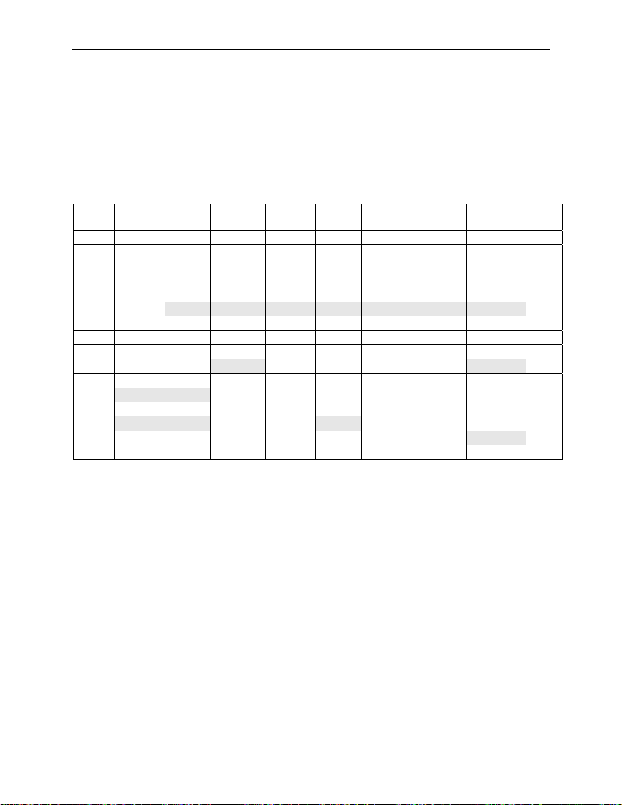
VDD
VDD
X12IN
X12OUT
GND
ROW0
ROW1
ROW2
ROW3
ROW4
ROW5
COL0
COL1
COL2
COL3
COL4
USR0
USR1
USR2
USR3
USR4
USR5
USR6
USR7
USR8
GND
TEST
PLL
and
TIMEBASES
12MHz
OSCILLATOR
KEYPAD
INTERFACE
DRIVERS
USR(8:0)
SEC
RESET
VOLTAGE REFERENCE
AND FUSE TRIM
CIRCUITRY
VPD REGULATOR
FLASH/ROM
PROGRAM
MEMORY
32KB
FLASH
INTERFACE
DATA
XRAM
2KB
VDD
ANA_IN
TCLK
MEMORY_
CONTROL
CONTROL
SCRATCH
CORE
PORTS
SERIAL
RXTX
ERST
ISBR
ICE INTERFACE
OCDSI
RAM_
SFR_
IRAM
256B
ALU
PMU
PERIPHERAL
INTERFACE
and SFR LOGIC
TBUS1
TBUS2
TBUS3
CONTROL
UNIT
TIMER_0_
1
WATCH-
DOG
TIMER
ISR
CONTROL
SMART CARD LOGIC
ISO UART and CLOCK GENERATOR
VPC
VCC
LOGIC
SMART
CARD
ISO
INTERFACE
EXTERNAL
SMART
CARD
INTERFACE
MASTER
I
INT.
VCC
GND
RST
CLK
I/O
AUX1
AUX2
PRES
PRESB
SCLK
SIO
INT2
INT3
2
C
SCL
SDA
TBUS0
LED
DRIVERS
Pins avaiable on both 68 and 44 pin packages.
Pins only avaiable on 68 pin package.
GND
TXD
RXD
LED1
LED0
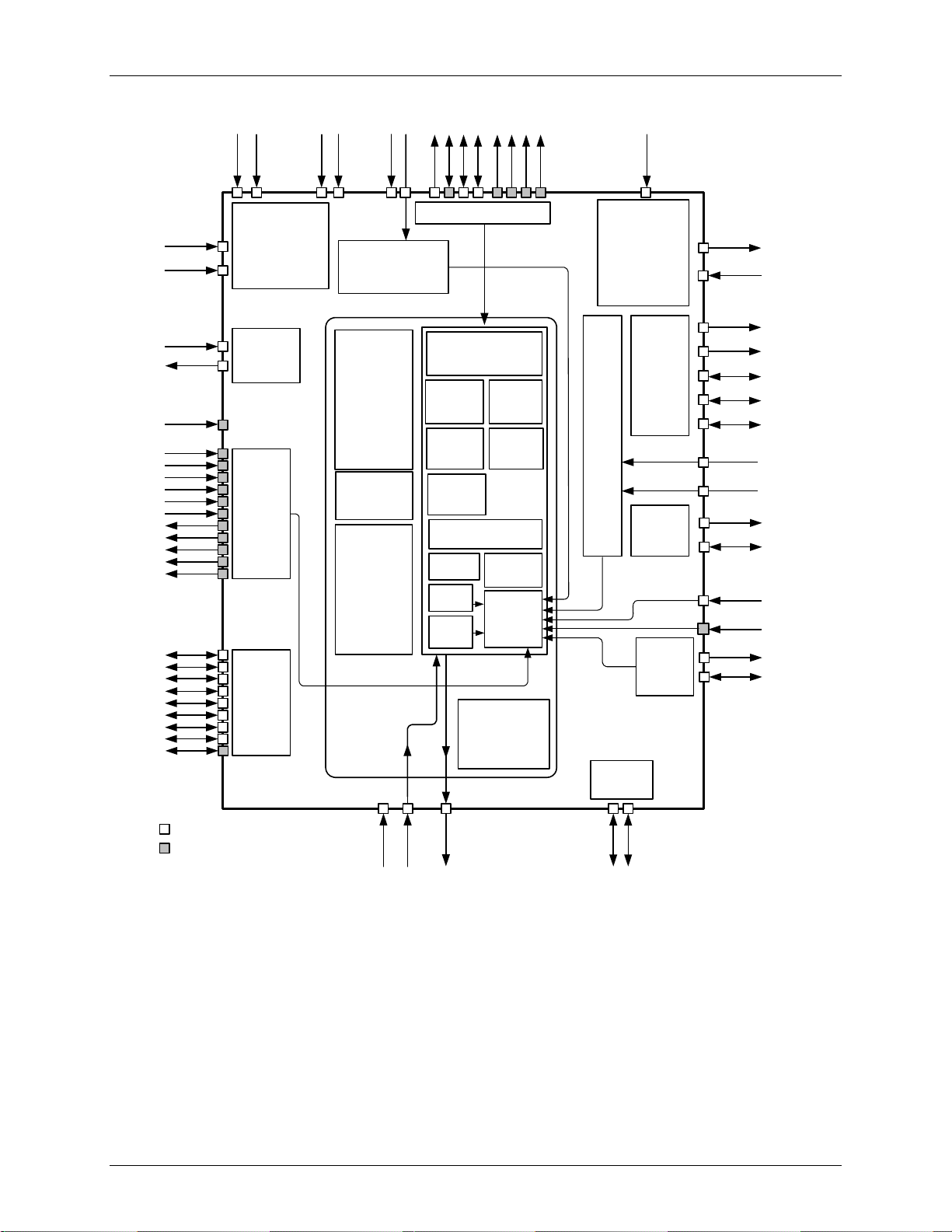
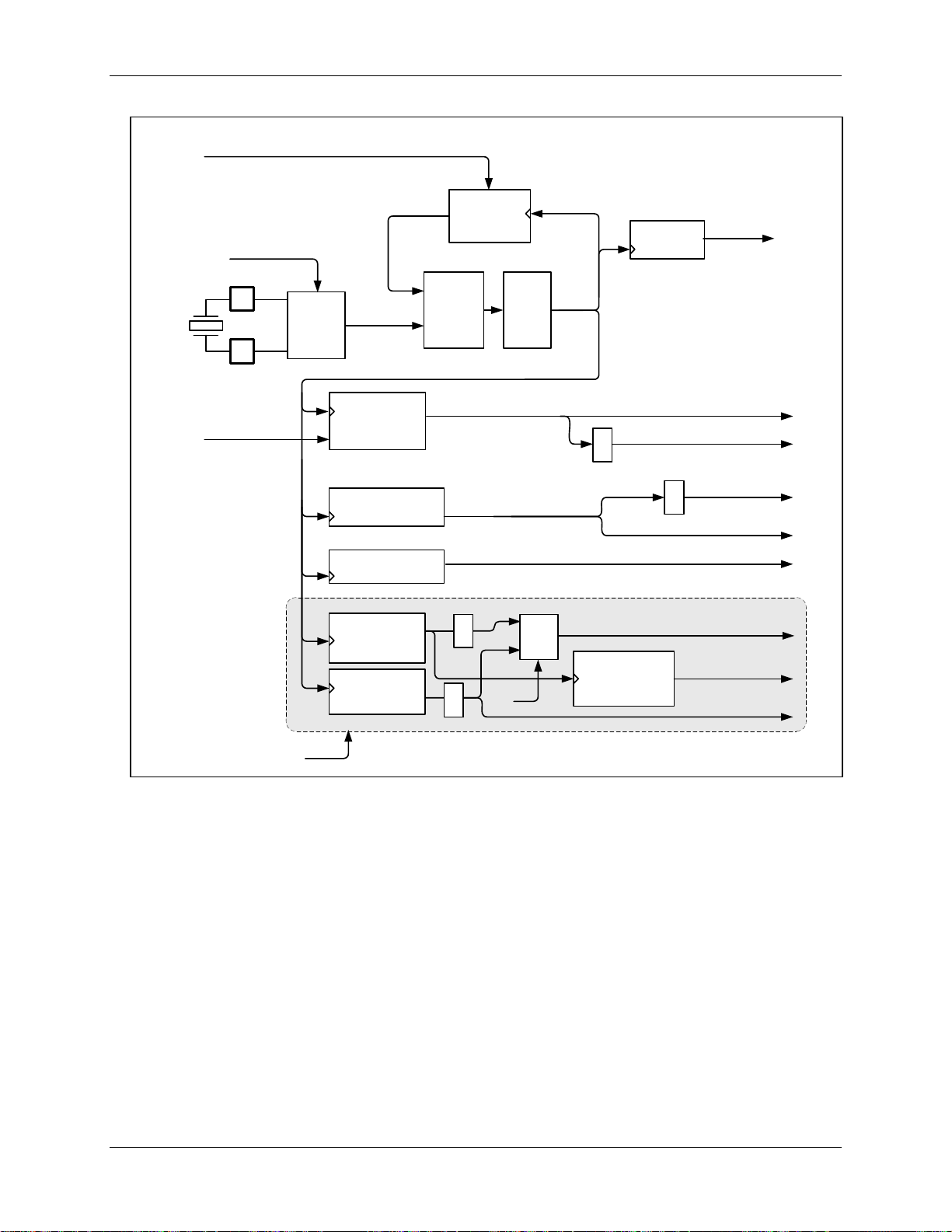
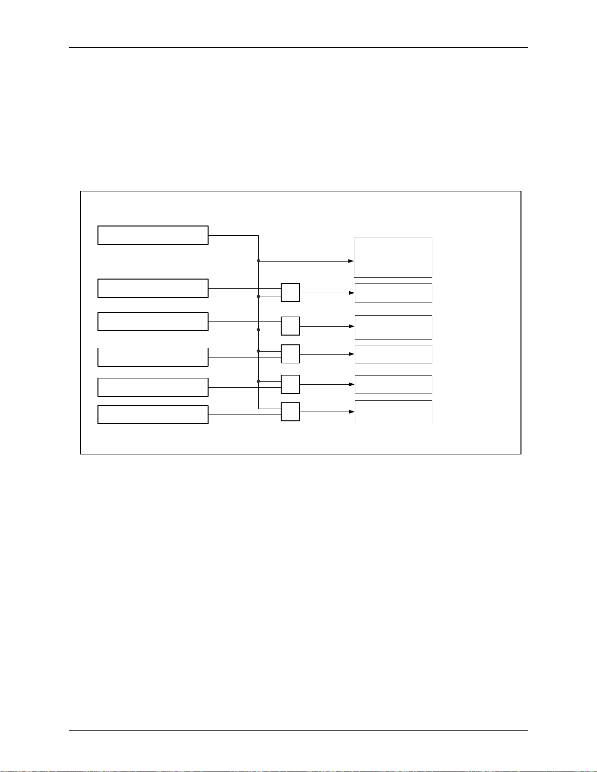
Figure 1: IC Functional Block Diagram
Rev. 1.2 7
73S1209F Data Sheet DS_1209F_004
1 Hardware Description
1.1 Pin Description
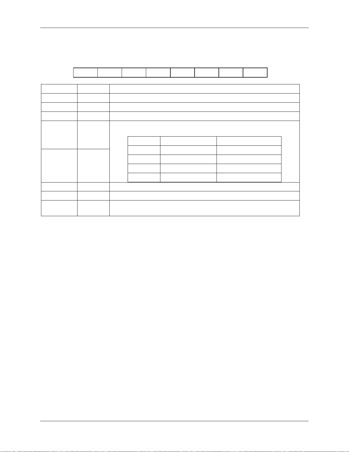
Table 1: 73S1209F Pinout Description
Pin Name
Pin (68 QFN)
Pin (44 QFN)
Type
X12IN 10 8 I
X12OUT 11 9 O Figure 26 MPU clock crystal oscillator output pin.
ROW (5:0)
0
1
2
3
4
5
COL(4:0)
0
1
2
3
4
USR(8:0)
0
1
2
3
4
5
6
7
8
SCL 5 5 O Figure 28 I2C (master mode) compatible Clock signal. Note: the
SDA 6 6 IO Figure 27 I2C (master mode) compatible data I/O. Note: this pin is
LED(1:0)
0
1
RXD 17 11 I Figure 31 Serial UART Receive data pin.
TXD 18 12 O Figure 28 Serial UART Transmit data pin.
INT3 51 I Figure 31 General purpose interrupt input.
21
22
24
34
37
38
12
13
14
16
19
36
35
33
31
30
29
23
20
32
1
3
I
O Figure 33 Keypad column output scan pins.
IO Figure 29 General-purpose user pins, individually configurable as
24
23
22
21
20
19
14
13
3 4 IO
Equivalent
Figure 26 MPU clock crystal oscillator input pin. A 1MΩ resistor is
Figure 32
Figure 34
Description
Circuit*
required between pins X12IN and X12OUT.
Keypad row input sense.
inputs or outputs or as external input interrupt ports.
pin is configured as an open drain output. When the
I2C interface is being used, an external pull up resistor
is required. A value of 3K is recommended.
bi-directional. When the pin is configured as output, it is
an open drain output. When the I2C interface is being
used, an external pull up resistor is required. A value of
3K is recommended.
Special output drivers, programmable pull-down current
to drive LEDs. May also be used as inputs.
8 Rev. 1.2

DS_1209F_004 73S1209F Data Sheet
Pin Name
Pin (68 QFN)
Pin (44 QFN)
Type
Equivalent
Description
Circuit*
INT2 52 32 I Figure 31 General purpose interrupt input.
SIO 50 31 IO Figure 27 IO data signal for use with external Smart Card interface
circuit such as 73S8010.
SCLK 48 30 O Figure 28 Clock signal for use with external Smart Card interface
circuit.
PRES 64 43 I Figure 39 Smart Card presence. Active high. Note: the pin has a
very weak pull down resistor. In noisy environments, an
external pull down may be desired to insure against a
false card event.
PRESB 56 35 I Figure 40 Smart Card presence. Active low. Note: the pin has a
very weak pull up resistor. In noisy environments, an
external pull up may be desired to insure against a false
card event.
CLK 57 36 O Figure 37 Smart card clock signal.
RST 59 38 O Figure 37 Smart card Reset signal.
IO 63 42 IO Figure 38 Smart card Data IO signal.
AUX1 62 41 IO Figure 38 Auxiliary Smart Card IO signal (C4).
AUX2 61 40 IO Figure 38 Auxiliary Smart Card IO signal (C8).
VCC 60 39 PSO
Smart Card VCC supply voltage output. A 0.47μF
capacitor is required and should be located at the smart
card connector. The capacitor should be a ceramic type
with low ESR.
GND 58 37 GND Smart Card Ground.
VPC 55 34 PSI Smart Card LDO regulator power supply source. A
10μF and a 0.1μF capacitor are required at the VPC
input. The 10μF capacitor should be a ceramic type
with low ESR.
TBUS(3:0)
0
1
2
3
53
49
47
43
IO
Trace bus signals for ICE.
RXTX 45 28 IO ICE control.
ERST 40 25 IO ICE control.
ISBR 68 IO ICE control.
TCLK 41 26 I ICE control.
Figure 36 Analog input pin. This signal goes to a programmable
ANA_IN 15 10 AI
comparator and is used to sense the value of an
external voltage.
SEC 67 2 I Figure 35 Input pin for use in programming security fuse. It should
be connected to ground when not in use.
TEST 54 33 DI Figure 35
Test pin, should be connected to ground.
Rev. 1.2 9
73S1209F Data Sheet DS_1209F_004
Pin Name
Pin (68 QFN)
Pin (44 QFN)
VDD 28
42
65
18
27
44
Type
I
Equivalent
Description
Circuit*
General positive power supply pins. All digital IO is
referred to this supply voltage. There is an on-chip
regulator that uses VDD to provide power for internal
circuits (VPD). A 0.1μF capacitor is recommended at
each VDD pin.
N/C 2
4
7
16
17
29
8
26
No connect.
27
39
46
GND 9
25
7
15
GND
General ground supply pins for all IO and logic circuits.
44
RESET 66 1 I Figure 31 Reset input, positive assertion. Resets logic and
registers to default condition.
* See the figures in the Equivalent Circuits section.
10 Rev. 1.2
DS_1209F_004 73S1209F Data Sheet
1.2 Hardware Overview
The 73S1209F single smart card controller integrates all primary functional blocks required to implement
a smart card reader. Included on chip are an 8051-compatible microprocessor (MPU) which executes up
to one instruction per clock cycle (80515), a fully integrated IS0-7816 compliant smart card interface,
expansion smart card interface, serial interface, I2C interface, 6 x 5 keypad interface, 2 LED drivers,
RAM, FLASH memory, and a variety of I/O pins. A functional block diagram of the 73S1209F is shown in
Figure 1.
1.3 80515 MPU Core
1.3.1 80515 Overview
The 73S1209F includes an 80515 MPU (8-bit, 8051-compatible) that performs most instructions in one
clock cycle. The 80515 architecture eliminates redundant bus states and implements parallel execution
of fetch and execution phases. Normally a machine cycle is aligned with a memory fetch, therefore, most
of the 1-byte instructions are performed in a single cycle. This leads to an 8x performance (average)
improvement (in terms of MIPS) over the Intel 8051 device running at the same clock frequency.
Actual processor clocking speed can be adjusted to the total processing demand of the application
(cryptographic calculations, key management, memory management, and I/O management) using the
XRAM special function register MPUCKCtl.
Typical smart card, serial, keyboard and I2C management functions are available for the MPU as part of
Teridian’s standard library. A standard ANSI “C” 80515-application programming interface library is
available to help reduce design cycle. Refer to the 73S12xxF Software User’s Guide.
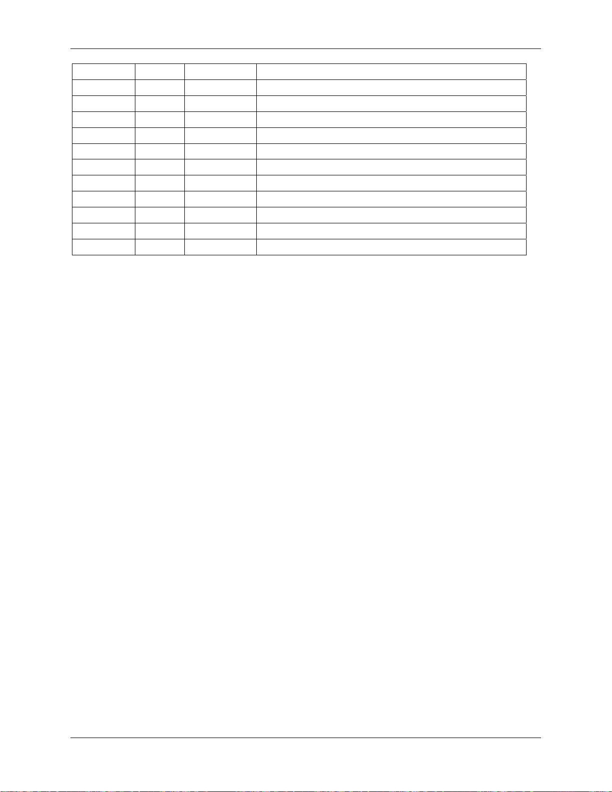
1.3.2 Memory Organization
The 80515 MPU core incorporates the Harvard architecture with separate code and data spaces.
Memory organization in the 80515 is similar to that of the industry standard 8051. There are three
memory areas: Program memory (Flash), external data memory (XRAM), and internal data memory
(IRAM). Data bus address space is allocated to on-chip memory as shown Table 2
Table 2: MPU Data Memory Map
Address
(hex)
0000-7FFF Flash Memory Non-volatile Program and non-volatile data 32KB
0000-07FF Static RAM Volatile MPU data XRAM 2KB
FC00-FFFF External SFR Volatile Peripheral control 1KB
Note: The IRAM is part of the core and is addressed differently.
Program Memory: The 80515 can address up to 32KB of program memory space from 0x0000 to
0x7FFF. Program memory is read when the MPU fetches instructions or performs a MOVC operation.
After reset, the MPU starts program execution from location 0x0000. The lower part of the program
memory includes reset and interrupt vectors. The interrupt vectors are spaced at 8-byte intervals, starting
from 0x0003. Reset is located at 0x0000.
Flash Memory: The program memory consists of flash memory. The flash memory is intended to
primarily contain MPU program code. Flash erasure is initiated by writing a specific data pattern to
specific SFR registers in the proper sequence. These special pattern/sequence requirements prevent
inadvertent erasure of the flash memory.
Memory
Technology
Memory Type Typical Usage
Memory Size
(bytes)
Rev. 1.2 11

73S1209F Data Sheet DS_1209F_004
The mass erase sequence is:
1. Write 1 to the FLSH_MEEN bit in the FLSHCTL register (SFR address 0xB2[1]).
2. Write pattern 0xAA to ERASE (SFR address 0x94).
Note: The mass erase cycle can only be initiated when the ICE port is enabled.
The page erase sequence is:
1. Write the page address to PGADDR (SFR address 0xB7[7:1])
2. Write pattern 0x55 to ERASE (SFR address 0x94)
The PGADDR register denotes the page address for page erase. The page size is 512 (200h) bytes and
there are 128 pages within the flash memory. The PGADDR denotes the upper seven bits of the flash
memory address such that bit 7:1 of the PGADDR corresponds to bit 15:9 of the flash memory address.
Bit 0 of the PGADDR is not used and is ignored. The MPU may write to the flash memory. This is one of
the non-volatile storage options available to the user. The FLSHCTL SFR bit FLSH_PWE (flash program
write enable) differentiates 80515 data store instructions (MOVX@DPTR,A) between Flash and XRAM
writes. Before setting FLSH_PWE, all interrupts need to be disabled by setting EAL = 1. Table 3 shows
the location and description of the 73S1209F flash-specific SFRs.
Any flash modifications must set the CPUCLK to operate at 3.6923 MHz (MPUCLKCtl = 0x0C)
before any flash memory operations are executed to insure the proper timing when modifying the
flash memory.
12 Rev. 1.2

DS_1209F_004 73S1209F Data Sheet
Table 3: Flash Special Function Registers
Register SFR
R/W Description
Address
ERASE 0x94 W This register is used to initiate either the Flash Mass Erase cycle or the
Flash Page Erase cycle. Specific patterns are expected for ERASE in
order to initiate the appropriate Erase cycle (default = 0x00).
0x55 – Initiate Flash Page Erase cycle. Must be proceeded by a write to
PGADDR @ SFR 0xB7.
0xAA – Initiate Flash Mass Erase cycle. Must be proceeded by a write
to FLSH_MEEN @ SFR 0xB2 and the debug port must be enabled.
Any other pattern written to ERASE will have no effect.
PGADDR 0xB7 R/W Flash Page Erase Address register containing the flash memory page
address (page 0 through 127) that will be erased during the Page Erase
cycle (default = 0x00). Note: the page address is shifted left by one bit
(see detailed description above).
Must be re-written for each new Page Erase cycle.
FLSHCTL 0xB2 R/W
Bit 0 (FLSH_PWE): Program Write Enable:
0 – MOVX commands refer to XRAM Space, normal operation (default).
1 – MOVX @DPTR,A moves A to Program Space (Flash) @ DPTR.
This bit is automatically reset after each byte written to flash. Writes to
this bit are inhibited when interrupts are enabled.
W Bit 1 (FLSH_MEEN): Mass Erase Enable:
0 – Mass Erase disabled (default).
1 – Mass Erase enabled.
Must be re-written for each new Mass Erase cycle.
R/W Bit 6 (SECURE):
Enables security provisions that prevent external reading of flash
memory and CE program RAM. This bit is reset on chip reset and may
only be set. Attempts to write zero are ignored.
Rev. 1.2 13
73S1209F Data Sheet DS_1209F_004
Internal Data Memory: The Internal data memory provides 256 bytes (0x00 to 0xFF) of data memory.
The internal data memory address is always one byte wide and can be accessed by either direct or
indirect addressing. The Special Function Registers occupy the upper 128 bytes. This SFR area is
available only by direct addressing. Indirect addressing accesses the upper 128 bytes of Internal
RAM.
The lower 128 bytes contain working registers and bit-addressable memory. The lower 32 bytes form
four banks of eight registers (R0-R7). Two bits on the program memory status word (PSW) select which
bank is in use. The next 16 bytes form a block of bit-addressable memory space at bit addressees 0x000x7F. All of the bytes in the lower 128 bytes are accessible through direct or indirect addressing. Table 4
shows the internal data memory map.
Table 4: Internal Data Memory Map
Address Direct Addressing Indirect Addressing
0xFF
0x80
Special Function
Registers (SFRs)
RAM
0x7F
0x30
Byte-addressable area
0x2F
0x20
Byte or bit-addressable area
0x1F
0x00
Register banks R0…R7 (x4)
External Data Memory: While the 80515 can address up to 64KB of external data memory in the space
from 0x0000 to 0xFFFF, only the memory ranges shown in Figure 2 contain physical memory. The
80515 writes into external data memory when the MPU executes a MOVX @Ri,A or MOVX @DPTR,A
instruction. The MPU reads external data memory by executing a MOVX A,@Ri or MOVX A,@DPTR
instruction.
There are two types of instructions, differing in whether they provide an eight-bit or sixteen-bit indirect
address to the external data RAM.
In the first type (MOVX A,@Ri), the contents of R0 or R1, in the current register bank, provide the eight
lower-ordered bits of address. This method allows the user access to the first 256 bytes of the 2KB of
external data RAM. In the second type of MOVX instruction (MOVX A,@DPTR), the data pointer
generates a sixteen-bit address.
14 Rev. 1.2
DS_1209F_004 73S1209F Data Sheet
Address Use
0x7FFF
Flash
Program
memory
32K
Bytes
0x0000
Address Use
0xFFFF
0XFF80
0xFF7F
0XFE00
0xFBFF
0x0800
0x07FF
Peripheral Control
Registers (128b)
Smart Card Control
(384b)
---
XRAM
0x0000
Address
0xFF
0x80
0x7F
0x48
0x47
0x20
0x1F
0x18
0x17
0x10
0x0F
0x08
0x07
0x00
Use
Indirect
Access
Direct
Access
Byte RAM SFRs
Byte RAM
Bit/Byte RAM
Register bank 3
Register bank 2
Register bank 1
Register bank 0
Program Memory
External Data Memory
Internal Data Memory
Figure 2: Memory Map
Dual Data Pointer: The Dual Data Pointer accelerates the block moves of data. The standard DPTR is a
16-bit register that is used to address external memory. In the 80515 core, the standard data pointer is
called DPTR, the second data pointer is called DPTR1. The data pointer select bit chooses the active
pointer. The data pointer select bit is located at the LSB of the DPS IRAM special function register
(DPS.0). DPTR is selected when DPS.0 = 0 and DPTR1 is selected when DPS.0 = 1.
The user switches between pointers by toggling the LSB of the DPS register. All DPTR-related
instructions use the currently selected DPTR for any activity.
Note: The second data pointer may not be supported by certain compilers.
Rev. 1.2 15

73S1209F Data Sheet DS_1209F_004
1.4 Program Security
Two levels of program and data security are available. Each level requires a specific fuse to be blown in
order to enable or set the specific security mode. Mode 0 security is enabled by setting the SECURE bit
(bit 6 of SFR register FLSHCTL 0xB2) Mode 0 limits the ICE interface to only allow bulk erase of the
flash program memory. All other ICE operations are blocked. This guarantees the security of the user’s
MPU program code. Security (Mode 0) is enabled by MPU code that sets the SECURE bit. The MPU
code must execute the setting of the SECURE bit immediately after a reset to properly enable Mode 0.
This should be the first instruction after the reset vector jump has been executed. If the “startup.a51”
assembly file is used in an application, then it must be modified to set the SECURE bit after the reset
vector jump. If not using “startup.a51”, then this should be the first instruction in main(). Once security
Mode 0 is enabled, the only way to disable it is to perform a global erase of the flash followed by a full
circuit reset. Once the flash has been erased and the reset has been executed, security Mode 0 is
disabled and the ICE has full control of the core. The flash can be reprogrammed after the bulk erase
operation is completed. Global erase of the flash will also clear the data XRAM memory. The security
enable bit (SECURE) is reset whenever the MPU is reset. Hardware associated with the bit only allows it
to be set. As a result, the code may set the SECURE bit to enable the security Mode 0 feature but may
not reset it. Once the SECURE bit is set, the code is protected and no external read of program code in
flash or data (in XRAM) is possible. In order to invoke the security Mode 0, the SECSET0 (bit 1 of XRAM
SFR register SECReg 0xFFD7) fuse must be blown beforehand or the security mode 0 will not be
enabled. The SECSET0 and SECSET1 fuses once blown, cannot be overridden.
Specifically, when SECURE is set:
• The ICE is limited to bulk flash erase only.
• Page zero of flash memory may not be page-erased by either MPU or ICE. Page zero may only be
erased with global flash erase. Note that global flash erase erases XRAM whether the SECURE bit is
set or not.
• Writes to page zero, whether by MPU or ICE, are inhibited.
Security mode 1 is in effect when the SECSET1 fuse has been programmed (blown open). In security
mode 1, the ICE is completely and permanently disabled. The Flash program memory and the MPU are
not available for alteration, observation, or control. As soon as the fuse has been blown, the ICE is
disabled. The testing of the SECSET1 fuse will occur during the reset and before the start of pre-boot
and boot cycles. This mode is not reversible, nor recoverable. In order to blow the SECSET1 fuse, the
SEC pin must be held high for the fuse burning sequence to be executed properly. The firmware can
check to see if this pin is held high by reading the SECPIN bit (bit 5 of XRAM SFR register SECReg
0xFFD7). If this bit is set and the firmware desires, it can blow the SECSET1 fuse. The burning of the
SECSET0 does not require the SEC pin to be held high.
In order to blow the fuse for SECSET1 and SECSET0, a particular set of register writes in a specific order
need to be followed. There are two additional registers that need to have a specific value written to them
in order for the desired fuse to be blown. These registers are FUSECtl (0xFFD2) and TRIMPCtl
(0xFFD1). The sequence for blowing the fuse is as follows:
1. Write 0x54H to FUSECtl.
2. Write 0x81H for security mode 0 Note: only program one security mode at a time.
Write 0x82H for security mode 1 Note: SEC pin must be high for security mode 1.
3. Write 0xA6 to TRIMPCtl.
4. Delay about 500 us
5. Write 0x00 to TRIMPCtl.
16 Rev. 1.2

DS_1209F_004 73S1209F Data Sheet
Table 5: Security Control Registers
Register SFR
R/W Description
Address
FLSHCTL 0xB2 R/W Bit 0 (FLSH_PWE): Program Write Enable:
0 – MOVX commands refer to XRAM Space, normal operation (default).
1 – MOVX @DPTR,A moves A to Program Space (Flash) @ DPTR.
This bit is automatically reset after each byte written to flash. Writes to this
bit are inhibited when interrupts are enabled.
W Bit 1 (FLSH_MEEN): Mass Erase Enable:
0 – Mass Erase disabled (default).
1 – Mass Erase enabled.
Must be re-written for each new Mass Erase cycle.
R/W Bit 6 (SECURE):
Enables security provisions that prevent external reading of flash memory
and CE program RAM. This bit is reset on chip reset and may only be set.
Attempts to write zero are ignored.
TRIMPCtl 0xFFD1 W 0xA6 value will cause the selected fuse to be blown. All other values will
stop the burning process.
FUSECtl 0xFFD2 W 0x54 value will set up for security fuse control. All other values are
reserved and should not be used.
SECReg 0xFFD7 W Bit 7 (PARAMSEC):
0 – Normal operation
1 – Enable permanent programming of the security fuses.
R Bit 5 (SECPIN):
Indicates the state of the SEC pin. The SEC pin is held low by a pull-down
resistor. The user can force this pin high during boot sequence time to
indicate to the firmware that sec mode 1 is desired.
R/W Bit 1 (SECSET1):
See Program Security section.
R/W Bit 0 (SECSET0):
See Program Security section.
Rev. 1.2 17
73S1209F Data Sheet DS_1209F_004
1.5 Special Function Registers (SFRs)
The 73S1209F utilizes numerous SFRs to communicate with the 73S1209F s many peripherals. This
results in the need for more SFR locations outside the direct address IRAM space (0x80 to 0xFF). While
some peripherals are mapped to unused IRAM SFR locations, additional SFRs for the smart card and
other peripheral functions are mapped to the top of the XRAM data space (0xFC00 to 0xFFFF).
1.5.1 Internal Data Special Function Registers (SFRs)
A map of the Special Function Registers is shown in Table 6.
Table 6: IRAM Special Function Registers Locations
Hex\
Bin
F8 FF
F0 B F7
E8 EF
E0 A E7
D8 BRCON DF
D0 PSW
C8 T2CON CF
C0 IRCON C7
B8 IEN1 IP1 S0RELH S1RELH BF
B0
A8 IEN0 IP0 S0RELL AF
A0
98 S0CON S0BUF IEN2 S1CON S1BUF S1RELL 9F
90
88 TCON TMOD TL0 TL1 TH0 TH1
80 SP DPL DPH DPL1 DPH1 WDTREL PCON 87
Only a few addresses are used, the others are not implemented. SFRs specific to the 73S1209F are
shown in bold print (gray background). Any read access to unimplemented addresses will return
undefined data, while most write access will have no effect. However, a few locations are reserved and
not user configurable in the 73S1209F. Writes to the unused SFR locations can affect the operation
of the core and therefore must not be written to. This applies to all the SFR areas in both the
IRAM and XRAM spaces. In addition, all unused bit locations within valid SFR registers must be
left in their default (power on default) states.
X000 X001 X010 X011 X100 X101 X110 X111
KCOL KROW KSCAN KSTAT KSIZE KORDERL KORDERH
ERASE
97
PGADDR
MCLKCtl
USR8 UDIR8
USR70 UDIR70
FLSHCTL
A7
DPS
Bin/
Hex
D7
B7
8F
18 Rev. 1.2

DS_1209F_004 73S1209F Data Sheet
1.5.2 IRAM Special Function Registers (Generic 80515 SFRs)
Table 7 shows the location of the SFRs and the value they assume at reset or power-up.
Table 7: IRAM Special Function Registers Reset Values
Name Location Reset Value Description
SP 0x81 0x07 Stack Pointer
DPL 0x82 0x00 Data Pointer Low 0
DPH 0x83 0x00 Data Pointer High 0
DPL1 0x84 0x00 Data Pointer Low 1
DPH1 0x85 0x00 Data Pointer High 1
WDTREL 0x86 0x00 Watchdog Timer Reload register
PCON 0x87 0x00 Power Control
TCON 0x88 0x00 Timer/Counter Control
TMOD 0x89 0x00 Timer Mode Control
TL0 0x8A 0x00 Timer 0, low byte
TL1 0x8B 0x00 Timer 1, high byte
TH0 0x8C 0x00 Timer 0, low byte
TH1 0x8D 0x00 Timer 1, high byte
MCLKCtl 0x8F 0x0A Master Clock Control
USR70 0x90 0xFF User Port Data (7:0)
UDIR70 0x91 0xFF User Port Direction (7:0)
DPS 0x92 0x00 Data Pointer select Register
ERASE 0x94 0x00 Flash Erase
S0CON 0x98 0x00 Serial Port 0, Control Register
S0BUF 0x99 0x00 Serial Port 0, Data Buffer
IEN2 0x9A 0x00 Interrupt Enable Register 2
S1CON 0x9B 0x00 Serial Port 1, Control Register
S1BUF 0x9C 0x00 Serial Port 1, Data Buffer
S1RELL 0x9D 0x00 Serial Port 1, Reload Register, low byte
USR8 0xA0 0x00 User Port Data (8)
UDIR8 0xA1 0x01 User Port Direction (8)
IEN0 0xA8 0x00 Interrupt Enable Register 0
IP0 0xA9 0x00 Interrupt Priority Register 0
S0RELL 0xAA 0xD9 Serial Port 0, Reload Register, low byte
FLSHCTL 0xB2 0x00 Flash Control
PGADDR 0xB7 0x00 Flash Page Address
IEN1 0xB8 0x00 Interrupt Enable Register 1
IP1 0xB9 0x00 Interrupt Priority Register 1
S0RELH 0xBA 0x03 Serial Port 0, Reload Register, high byte
S1RELH 0xBB 0x03 Serial Port 1, Reload Register, high byte
IRCON 0xC0 0x00 Interrupt Request Control Register
T2CON 0xC8 0x00 Timer 2 Control
Rev. 1.2 19
73S1209F Data Sheet DS_1209F_004
Name Location Reset Value Description
PSW 0xD0 0x00 Program Status Word
KCOL 0XD1 0x1F Keypad Column
KROW 0XD2 0x3F Keypad Row
KSCAN 0XD3 0x00 Keypad Scan Time
KSTAT 0XD4 0x00 Keypad Control/Status
KSIZE 0XD5 0x00 Keypad Size
KORDERL 0XD6 0x00 Keypad Column LS Scan Order
KORDERH 0XD7 0x00 Keypad Column MS Scan Order
BRCON 0xD8 0x00 Baud Rate Control Register (only BRCON.7 bit used)
A 0xE0 0x00 Accumulator
B 0xF0 0x00 B Register
20 Rev. 1.2

DS_1209F_004 73S1209F Data Sheet
1.5.3 External Data Special Function Registers (SFRs)
A map of the XRAM Special Function Registers is shown in Table 6. . The smart card registers are listed
separately in Table 108.
Table 8: XRAM Special Function Registers Reset Values
Name Location Reset Value Description
DAR 0x FF80 0x00 Device Address Register (I2C)
WDR 0x FF81 0x00 Write Data Register (I2C)
SWDR 0x FF82 0x00 Secondary Write Data Register (I2C)
RDR 0x FF83 0x00 Read Data Register (I2C)
SRDR 0x FF84 0x00 Secondary Read Data Register (I2C)
CSR 0x FF85 0x00 Control and Status Register (I2C)
USRIntCtl1 0x FF90 0x00 External Interrupt Control 1
USRIntCtl2 0x FF91 0x00 External Interrupt Control 2
USRIntCtl3 0x FF92 0x00 External Interrupt Control 3
USRIntCtl4 0x FF93 0x00 External Interrupt Control 4
INT5Ctl 0x FF94 0x00 External Interrupt Control 5
INT6Ctl 0x FF95 0x00 External Interrupt Control 6
MPUCKCtl 0x FFA1 0x0C MPU Clock Control
ACOMP 0x FFD0 0x00 Analog Compare Register
TRIMPCtl 0x FFD1 0x00 TRIM Pulse Control
FUSECtl 0x FFD2 0x00 FUSE Control
VDDFCtl 0x FFD4 0x00 VDDFault Control
SECReg 0x FFD7 0x00 Security Register
MISCtl0 0x FFF1 0x00 Miscellaneous Control Register 0
MISCtl1 0x FFF2 0x10 Miscellaneous Control Register 1
LEDCtl 0x FFF3 0xFF LED Control Register
Accumulator (ACC, A): ACC is the accumulator register. Most instructions use the accumulator to hold
the operand. The mnemonics for accumulator-specific instructions refer to accumulator as “A”, not ACC.
B Register: The B register is used during multiply and divide instructions. It can also be used as a
scratch-pad register to hold temporary data.
Rev. 1.2 21
73S1209F Data Sheet DS_1209F_004
Program Status Word (PSW):
Table 9: PSW Register Flags
MSB LSB
CV AC F0 RS1 RS OV – P
Bit Symbol Function
PSW.7 CV Carry flag.
PSW.6 AC Auxiliary Carry flag for BCD operations.
PSW.5 F0 General purpose Flag 0 available for user.
PSW.4 RS1 Register bank select control bits. The contents of RS1 and RS0 select
the working register bank:
RS1/RS0 Bank Selected Location
PSW.3 RS0
00 Bank 0 (0x00 – 0x07)
01 Bank 1 (0x08 – 0x0F)
10 Bank 2 (0x10 – 0x17)
11 Bank 3 (0x18 – 0x1F)
PSW.2 OV Overflow flag.
PSW.1 F1 General purpose Flag 1 available for user.
PSW.0 P Parity flag, affected by hardware to indicate odd / even number of “one”
bits in the Accumulator, i.e. even parity.
Stack Pointer (SP): The stack pointer is a 1-byte register initialized to 0x07 after reset. This register is
incremented before PUSH and CALL instructions, causing the stack to begin at location 0x08.
Data Pointer: The data pointer (DPTR) is 2 bytes wide. The lower part is DPL, and the highest is DPH.
It can be loaded as a 2-byte register (MOV DPTR,#data16) or as two registers (e.g. MOV DPL,#data8). It
is generally used to access external code or data space (e.g. MOVC A,@A+DPTR or MOVX A,@DPTR
respectively).
Program Counter: The program counter (PC) is 2 bytes wide initialized to 0x0000 after reset. This
register is incremented during the fetching operation code or when operating on data from program
memory. Note: The program counter is not mapped to the SFR area.
Port Registers: The I/O ports are controlled by Special Function Registers USR70 and USR8. The
contents of the SFR can be observed on corresponding pins on the chip. Writing a 1 to any of the ports
(see Table 10) causes the corresponding pin to be at high level (3.3V), and writing a 0 causes the
corresponding pin to be held at low level (GND). The data direction registers UDIR70 and UDIR8 define
individual pins as input or output pins (see the User (USR) Ports section for details).
22 Rev. 1.2
DS_1209F_004 73S1209F Data Sheet
Table 10: Port Registers
Register
USR70 0x90 R/W Register for User port bit 7:0 read and write operations (pins USR0…
UDIR70 0x91 R/W Data direction register for User port bits 0:7. Setting a bit to 0 means that
USR8 0xA0 R/W Register for User port bit 8 read and write operations (pin *USR8).
UDIR8 0xA1 R/W Data direction register for port 1.
All ports on the chip are bi-directional. Each consists of a Latch (SFR USR70 to USR8), an output driver,
and an input buffer, therefore the MPU can output or read data through any of these ports if they are not
used for alternate purposes.
SFR
Address
R/W Description
USR7).
the corresponding pin is an output.
1.6 Instruction Set
All instructions of the generic 8051 microcontroller are supported. A complete list of the instruction set
and of the associated op-codes is contained in the 73S12xxF Software User’s Guide.
1.7 Peripheral Descriptions
1.7.1 Oscillator and Clock Generation
The 73S1209F has a single oscillator circuit for the main CPU clock. The oscillator circuit is designed to
operate with various crystal or external clock frequencies. An internal divider working in conjunction with
a PLL and VCO provides a 96MHz internal clock within the 73S1209F. 96 MHz is the recommended
frequency for proper operation of specific peripheral blocks such as the specific timers, ISO-7816 UART
and interfaces and keypad. The clock generation and control circuits are shown in Figure 3.
Rev. 1.2 23
73S1209F Data Sheet DS_1209F_004
MCount(2:0)
X12IN
X12OUT
CPUCKDiv
12.00MHz
HOSCen
12.00MHz
M DIVIDER
/(2*N + 4)
Phase
HIGH
XTAL
HCLK
Freq
DET
OSC
CPU CLOCK
DIVIDER
1.5-48MHz
7.386MHz
6 bits
DIVIDE
by 120
DIVIDE
by 96
SC/SCE
CLOCK
div 2
Prescaler 6bits
SCLK
CLOCK
Prescaler 6bits
See SC Clock descriptions for more accurate diagram
div 2
VCO
SELSC
SEL
MCLK
96MHz
DIVIDER
/93760
MPU CLOCK - CPCLK
div 2
SMART CARD LOGIC
ETU CLOCK
DIVIDER
12 bits
KEYCLK
1kHz
ICLK
7.386MHz
3.6923MHz
I2CCLK
div 2
400kHz
I2C_2x
800kHz
CLK1M
BLOCK CLOCK
SCCLK
ETUCLK
SCECLK
1MHz
SCCKenb
Figure 3: Clock Generation and Control Circuits
24 Rev. 1.2
DS_1209F_004 73S1209F Data Sheet
The master clock control register enables different sections of the clock circuitry and specifies the value
of the VCO Mcount divider. The MCLK must be configured to operate at 96MHz to ensure proper
operation of some of the peripheral blocks according to the following formula:
MCLK = (Mcount * 2 + 4) * F
= 96MHz
XTAL
Mcount is configured in the MCLKCtl register must be bound between a value of 1 to 7. The possible
crystal or external clock frequencies for getting MCLK = 96MHz are shown in Table 11.
Table 11: Frequencies and Mcount Values for MCLK = 96MHz
F
(MHz) Mcount (N)
XTAL
12.00 2
9.60 3
8.00 4
6.86 5
6.00 6
Master Clock Control Register (MCLKCtl): 0x8F Å 0x0A
Table 12: The MCLKCtl Register
MSB LSB
HSOEN KBEN SCEN – – MCT.2 MCT.1 MCT.0
Bit Symbol Function
MCLKCtl.7 HSOEN
High-speed oscillator disable. When set = 1, disables the high-speed crystal
oscillator and VCO/PLL system. Do not set this bit = 1.
MCLKCtl.6 KBEN 1 = Disable the keypad logic clock.
MCLKCtl.5 SCEN 1 = Disable the smart card logic clock.
MCLKCtl.4 –
MCLKCtl.3 –
MCLKCtl.2 MCT.2 This value determines the ratio of the VCO frequency (MCLK) to the high-
MCLKCtl.1 MCT.1
MCLKCtl.0 MCT.0
speed crystal oscillator frequency such that:
MCLK = (MCount*2 + 4)* F
. The default value is MCount = 2h such that
XTAL
MCLK = (2*2 + 4)*12.00MHz = 96MHz.
The MPU clock that drives the CPU core defaults to 3.6923MHz after reset. The MPU clock is scalable
by configuring the MPU Clock Control register.
Rev. 1.2 25
73S1209F Data Sheet DS_1209F_004
MPU Clock Control Register (MPUCKCtl): 0xFFA1 Å 0x0C
Table 13: The MPUCKCtl Register
MSB LSB
– – MDIV.5 MDIV.4 MDIV.3 MDIV.2 MDIV.1 MDIV.0
Bit Symbol Function
MPUCKCtl.7 –
MPUCKCtl.6 –
MPUCKCtl.5 MDIV.5
MPUCKCtl.4 MDIV.4
MPUCKCtl.3 MDIV.3
MPUCKCtl.2 MDIV.2
MPUCKCtl.1 MDIV.1
MPUCKCtl.0 MDIV.0
The oscillator circuits are designed to connect directly to standard parallel resonant crystal in a Pierce
oscillator configuration. Each side of the crystal should include a 22pF capacitor to ground for both
oscillator circuits and a 1MΩ resistor is required across the 12MHz crystal.
The CPU clock is available as an output on pin CPUCLK (68-pin version only).
This value determines the ratio of the MPU master clock frequency to
the VCO frequency (MCLK) such that
MPUClk = MCLK/(2 * (MPUCKDiv(5:0) + 1)).
Do not use values of 0 or 1 for MPUCKDiv(n).
Default is 0Ch to set CPCLK = 3.6923MHz.
73S1209F
X12IN
1MΩ
12MHz
22pF 22pF
Note: The crystal should be placed as close as possible to the IC, and vias should be avoided.
Figure 4: Oscillator Circuit
X12OUT
26 Rev. 1.2
DS_1209F_004 73S1209F Data Sheet
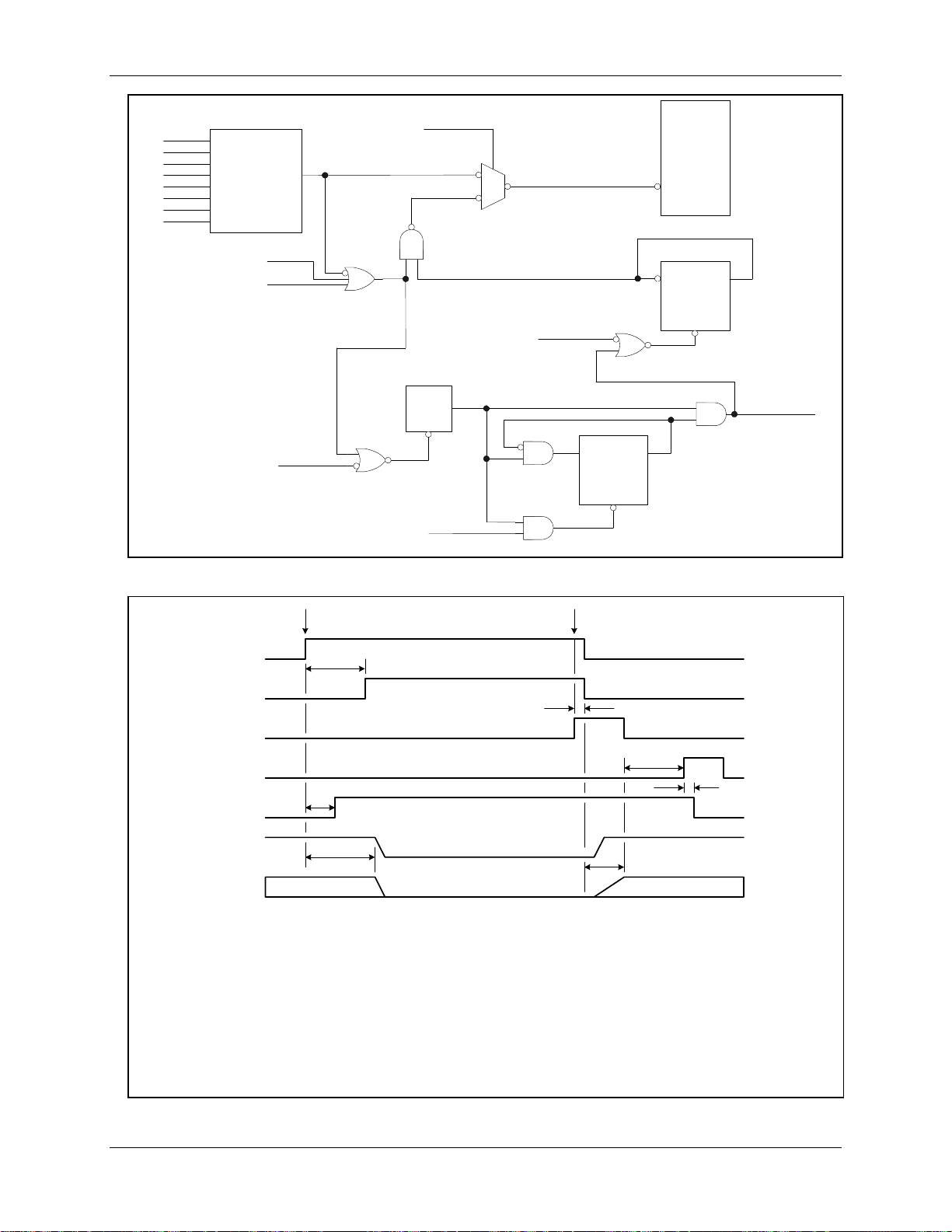
1.7.2 Power Control Modes
The 73S1209F contains circuitry to disable portions of the device and place it into lower power standby
modes. This is accomplished by either shutting off the power or disabling the clock going to the block.
The miscellaneous control registers MISCtl0, MISCtl1 and the Master Clock Control register (MCLKCtl)
provide control over the power modes. There is also a device power down mode that will stop the core,
clock subsystem and the peripherals connected to it. The PWRDN bit in MISCtl0 will setup the
73S1209F for power down and disable all clocks. The power down mode should only be initiated by
setting the PWRDN bit in the MISCtl0 register and not by manipulating individual control bits in various
registers. Figure 5 shows how the PWRDN bit controls the various functions that comprise power down
state.
state.
Figure 5 shows how the PWRDN bit controls the various functions that comprise power down
Note: the PWRDN Signal is not the direct version of the PWRDN Bit. There are delays from assertion of the
PWRDN bit to the assertion of the PWRDN Signal (32 MPU clocks) Refer to the Power Down sequence diagram.
MISCtl0 - PWRDN
VDDFCtl - VDDFEN
ACOMP - CMPEN
MCLCKCtl - HOSEN
SCVCCCtl - SCPRDN
MISCtl1 - FRPEN
These are the registers and
the names of the control bits.
PWRDN Signal
+
+
+
+
+
Analog functions
(VCO, PLL,
reference and bias
circuits, etc.)
VDDFAULT
ANALOG
COMPARE
High Speed OSC
Smart Card Power
Flash Read Pulse
one-shot circuit
These are the
block references.
Figure 5: Power-Down Control
When the PWRDN bit is set, the clock subsystem will provide a delay of 32 MPUCLK cycles to allow the
program to set the STOP bit in the PCON register. This delay will enable the program to properly halt the
core before the analog circuits shut down (high speed oscillator, VCO/PLL, voltage reference and bias
circuitry, etc.). The PDMUX bit in SFR INT5Ctl should be set prior to setting the PWRDN bit in order to
configure the wake up interrupt logic. The power down mode is de-asserted by any of the interrupts
connected to external interrupts 0, 4 and 5 (external USR[0:7], smart card and Keypad). These interrupt
sources are OR’ed together and routed through some delay logic into INT0 to provide this functionality.
The interrupt will turn on the power to all sections that were shut off and start the clock subsystem. After
the clock subsystem clocks start running, the MPUCLK begins to clock a 512 count delay counter. When
the counter times out, the interrupt will then be active on INT0 and the program can resume. Figure 6
shows the detailed logic for waking up the 73S1209F from a power down state using these specific
interrupt sources. Figure 7 shows the timing associated with the power down mode.
Rev. 1.2 27
73S1209F Data Sheet DS_1209F_004
PDMUX
USR0
USR1
USR2
USR3
USR4
USR5
USR6
USR7
USR[7:0] Control
USRxINTSrc set to
4(ext INT0 high)
or
6(ext INT0 low)
INT4
INT5
(FF94h:bit7)
MPU
0
1
INT0
CE
9 BIT CNTR
TC
CLR
PWRDN_analogQ
RESETB
Notes:
1. The counters are clocked by the MPUCLK
2. TC - Terminal count (high at overflow)
3. CE - Count enable
D
CLR
RESETB
PWRDN
(FFF1h:bit7)
RESETB
CE
5 BIT CNTR
CLR
TC
Figure 6: Detail of Power-Down Interrupt Logic
text
t4
t6
t7
PWRDN BIT
PWRDN SIG
EXT. EVENT
INT0 to MPU
MPU STOP
t0
t1
t2
ANALOG Enable
PLL CLOCKS
t3
t5
t0: MPU sets PWRDN bit.
t1: 32 MPU clock cycles after t0, the PWRDN SIG is asserted, turning all analog functions OFF.
t2: MPU executes STOP instruction, must be done prior to t1.
t3: Analog functions go to OFF condition. No Vref, PLL/VCO, Ibias, etc.
text: An external event (RTC, Keypad, Card event, USB) occurs.
t4: PWRDN bit and PWRDN signal are cleared by external event.
t5: High-speed oscillator/PLL/VCO operating.
t6: After 512 MPU clock cycles, INT0 to MPU is asserted.
t7: INT0 causes MPU to exit STOP condition.
Figure 7: Power-Down Sequencing
28 Rev. 1.2
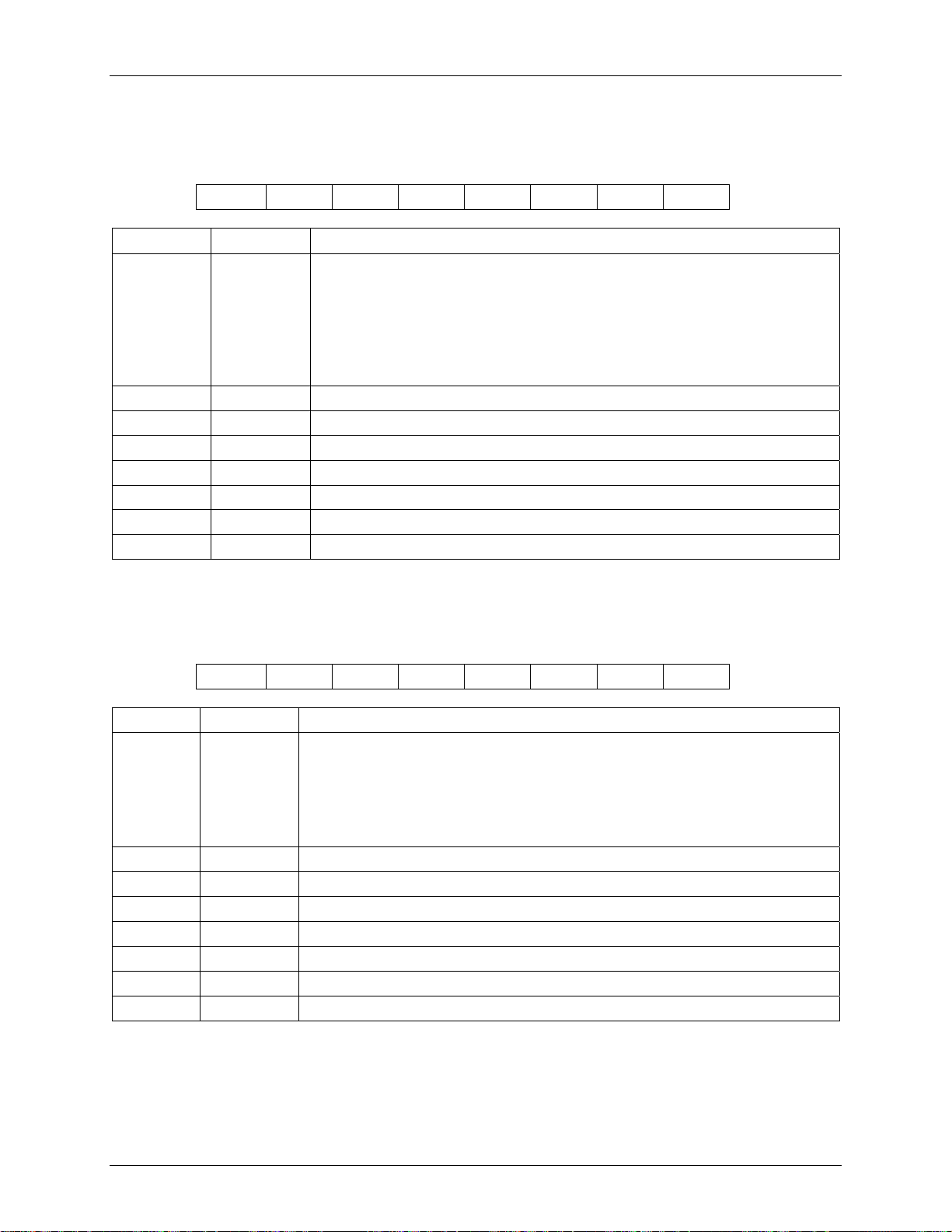
DS_1209F_004 73S1209F Data Sheet
External Interrupt Control Register (INT5Ctl): 0xFF94 Å 0x00
Table 14: The INT5Ctl Register
MSB LSB
PDMUX – – – – – KPIEN KPINT
Bit Symbol Function
When set=1, enables interrupts from Keypad (normally going to int5),
Smart Card interrupts (normally going to int4), or USR(7:0) pins (int0) to
cause interrupt on int0. The assertion of the interrupt to int0 is delayed by
INT5Ctl.7 PDMUX
512 MPU clocks to allow the analog circuits, including the clock system, to
stabilize. This bit must be set prior to asserting the PWRDN bit in order to
properly configure the interrupts that will wake up the circuit. This bit is
reset=0 when this register is read.
INT5Ctl.6 –
INT5Ctl.5 –
INT5Ctl.4 –
INT5Ctl.3 –
INT5Ctl.2 –
INT5Ctl.1 KPIEN Keypad interrupt enable.
INT5Ctl.0 KPINT Keypad interrupt flag.
Miscellaneous Control Register 0 (MISCtl0): 0xFFF1 Å 0x00
Table 15: The MISCtl0 Register
MSB LSB
PWRDN – – – – – SLPBK SSEL
Bit Symbol Function
This bit sets the circuit into a low-power condition. All analog (high speed
oscillator and VCO/PLL) functions are disabled 32 MPU clock cycles after
MISCtl0.7 PWRDN
this bit is set=1. This allows time for the next instruction to set the STOP bit
in the PCON register to stop the CPU core. The MPU is not operative in this
mode. When set, this bit overrides the individual control bits that otherwise
control power consumption.
MISCtl0.6 –
MISCtl0.5 –
MISCtl0.4 –
MISCtl0.3 –
MISCtl0.2 –
MISCtl0.1 SLPBK UART loop back testing mode.
MISCtl0.0 SSEL Serial port pins select.
Rev. 1.2 29
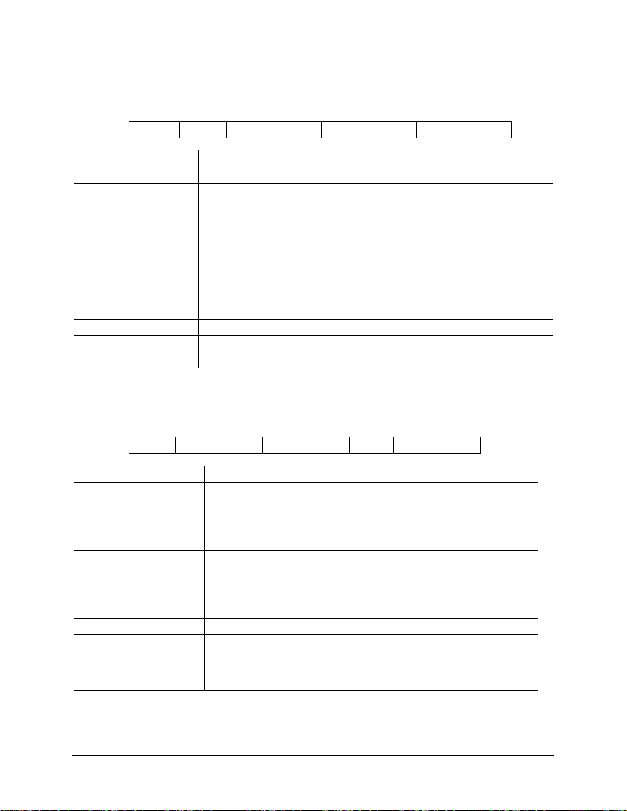
73S1209F Data Sheet DS_1209F_004
Miscellaneous Control Register 1 (MISCtl1): 0xFFF2 Å 0x10
Table 16: The MISCtl1 Register
MSB LSB
– – FRPEN FLSH66 – – – –
Bit Symbol Function
MISCtl1.7 –
MISCtl1.6 –
Flash Read Pulse enable (low). If FRPEN=1, the Flash Read signal is
passed through with no change. When FRPEN=0, a one-shot circuit that
MISCtl1.5 FRPEN
shortens the Flash Read signal is enabled to save power. The Flash Read
pulse will shorten to 40 or 66ns (approximate based on the setting of the
FLSH66 bit) in duration, regardless of the MPU clock rate. For MPU clock
frequencies greater than 10MHz, this bit should be set high.
MISCtl1.4 FLSH66
When high, creates a 66ns Flash read pulse, otherwise creates a 40ns read
pulse when FRPEN is set.
MISCtl1.3 –
MISCtl1.2 –
MISCtl1.1 –
MISCtl1.0 –
Master Clock Control Register (MCLKCtl): 0x8F Å 0x0A
Table 17: The MCLKCtl Register
MSB LSB
HSOEN KBEN SCEN – – MCT.2 MCT.1 MCT.0
Bit Symbol Function
High-speed oscillator enable. When set = 1, disables the high-speed
MCLKCtl.7 HSOEN*
crystal oscillator and VCO/PLL system. This bit is not changed when
the PWRDN bit is set but the oscillator/VCO/PLL is disabled.
MCLKCtl.6 KBEN
1 = Disable the keypad logic clock. This bit is not changed in PWRDN
mode but the function is disabled.
1 = Disable the smart card logic clock. This bit is not changed in
MCLKCtl.5 SCEN
PWRDN mode but the function is disabled. Interrupt logic for card
insertion/removal remains operable even with smart card clock
disabled.
MCLKCtl.4 –
MCLKCtl.3 –
MCLKCtl.2 MCT.2 This value determines the ratio of the VCO frequency (MCLK) to the
MCLKCtl.1 MCT.1
high-speed crystal oscillator frequency such that:
MCLK=(MCount*2 + 4)*Fxtal. The default value is MCount= 2h such
MCLKCtl.0 MCT.0
that MCLK = (2*2 + 4)*12.00MHz = 96MHz.
*Note: The HSOEN bit should never be set under normal circumstances. Power down control should
only be initiated via use of the PWRDN bit in MISCtl0.
30 Rev. 1.2

DS_1209F_004 73S1209F Data Sheet
Power Control Register 0 (PCON): 0x87 Å 0x00
The SMOD bit used for the baud rate generator is setup via this register.
Table 18: The PCON Register
MSB LSB
SMOD – – – GF1 GF0 STOP IDLE
Bit Symbol Function
PCON.7 SMOD If SM0D = 1, the baud rate is doubled.
PCON.6 –
PCON.5 –
PCON.4 –
PCON.3 GF1 General purpose flag 1.
PCON.2 GF0 General purpose flag 1.
PCON.1 STOP Sets CPU to Stop mode.
PCON.0 IDLE Sets CPU to Idle mode.
Rev. 1.2 31

73S1209F Data Sheet DS_1209F_004
1.7.3 Interrupts
The 80515 core provides 10 interrupt sources with four priority levels. Each source has its own request
flag(s) located in a special function register (TCON, IRCON, and SCON). Each interrupt requested by the
corresponding flag can be individually enabled or disabled by the enable bits in SFRs IEN0, IEN1, and
IEN2. Some of the 10 sources are multiplexed in order to expand the number of interrupt sources.
IEN2. Some of the 10 sources are multiplexed in order to expand the number of interrupt sources.
These will be described in more detail in the respective sections.
These will be described in more detail in the respective sections.
External interrupts are the interrupts external to the 80515 core, i.e. signals that originate in other parts of
External interrupts are the interrupts external to the 80515 core, i.e. signals that originate in other parts of
the 73S1209F, for example the USR I/O, smart card interface, analog comparators, etc. The external
the 73S1209F, for example the USR I/O, smart card interface, analog comparators, etc. The external
interrupt configuration is shown in Figure 8.
interrupt configuration is shown in Figure 8.
USR0
USR1
USR2
USR3
USR4
USR5
USR6
USR7
INT2
INT3
USR
Pads
INT
Pads
USR
USR
Int
Ctl
USR
USR
Int
Int
Ctl
Ctl
PDMUXCtl
0
Int
Ctl
+
1
Delay
Clear PWRDN bit
t0
int0
t1
int1
int2
int3
Card_Det
VCC_OK
CRDCtl
Wait Timeout
Card Event
+
VCC_TMR
VccCTL
KeyPad
I2C
Analog
Comp
Serial
Ch 0
Serial
Ch 1
VDD_Fault
RxData
TX_Event
Tx_Sent
TX_Error
RX_Error
SCInt
During STOP, IDLE
when PWRDN bit is set
INT5
Ctl
INT6
Ctl
SCIE
Figure 8: External Interrupt Configuration
+
int4
MPU
CORE
int5
int6
SerChan 0 int
SerChan 1 int
32 Rev. 1.2

DS_1209F_004 73S1209F Data Sheet
1.7.3.1 Interrupt Overview
When an interrupt occurs, the MPU will vector to the predetermined address as shown in Table 32. Once
the interrupt service has begun, it can only be interrupted by a higher priority interrupt. The interrupt
service is terminated by a return from the RETI instruction. When a RETI is performed, the processor will
return to the instruction that would have been next when the interrupt occurred.
When the interrupt condition occurs, the processor will also indicate this by setting a flag bit. This bit is
set regardless of whether the interrupt is enabled or disabled. Each interrupt flag is sampled once per
machine cycle, then samples are polled by the hardware. If the sample indicates a pending interrupt
when the interrupt is enabled, then the interrupt request flag is set. On the next instruction cycle, the
interrupt will be acknowledged by hardware forcing an LCALL to the appropriate vector address.
Interrupt response will require a varying amount of time depending on the state of the MPU when the
interrupt occurs. If the MPU is performing an interrupt service with equal or greater priority, the new
interrupt will not be invoked. In other cases, the response time depends on the current instruction. The
fastest possible response to an interrupt is 7 machine cycles. This includes one machine cycle for
detecting the interrupt and six cycles to perform the LCALL.
1.7.3.2 Special Function Registers for Interrupts
Interrupt Enable 0 Register (IEN0): 0xA8 Å 0x00
Table 19: The IEN0 Register
MSB LSB
EAL WDT – ES0 ET1 EX1 ET0 EX0
Bit Symbol Function
IEN0.7 EAL EAL = 0 – disable all interrupts.
IEN0.6 WDT Not used for interrupt control.
IEN0.5 –
IEN0.4 ES0 ES0 = 0 – disable serial channel 0 interrupt.
IEN0.3 ET1 ET1 = 0 – disable timer 1 overflow interrupt.
IEN0.2 EX1 EX1 = 0 – disable external interrupt 1.
IEN0.1 ET0 ET0 = 0 – disable timer 0 overflow interrupt.
IEN0.0 EX0 EX0 = 0 – disable external interrupt 0.
Rev. 1.2 33

73S1209F Data Sheet DS_1209F_004
Interrupt Enable 1 Register (IEN1): 0xB8 Å 0x00
Table 20: The IEN1 Register
MSB LSB
– SWDT EX6 EX5 EX4 EX3 EX2 –
Bit Symbol Function
IEN1.7 –
IEN1.6 SWDT Not used for interrupt control.
IEN1.5 EX6 EX6 = 0 – disable external interrupt 6.
IEN1.4 EX5 EX5 = 0 – disable external interrupt 5.
IEN1.3 EX4 EX4 = 0 – disable external interrupt 4.
IEN1.2 EX3 EX3 = 0 – disable external interrupt 3.
IEN1.1 EX2 EX2 = 0 – disable external interrupt 2.
IEN1.0 –
Interrupt Enable 2 Register (IEN2): 0x9A Å 0x00
Table 21: The IEN2 Register
MSB LSB
– – – – – – – ES1
Bit Symbol Function
IEN2.0 ES1 ES1 = 0 – disable serial channel interrupt.
34 Rev. 1.2

DS_1209F_004 73S1209F Data Sheet
Timer/Counter Control Register (TCON): 0x88 Å 0x00
Table 22: The TCON Register
MSB LSB
TF1 TR1 TF0 TR0 IE1 IT1 IE0 IT0
Bit Symbol Function
TCON.7 TF1 Timer 1 overflow flag.
TCON.6 TR1 Not used for interrupt control.
TCON.5 TF0 Timer 0 overflow flag.
TCON.4 TR0 Not used for interrupt control.
TCON.3 IE1 Interrupt 1 edge flag is set by hardware when the falling edge on external
interrupt int1 is observed. Cleared when an interrupt is processed.
TCON.2 IT1 Interrupt 1 type control bit. 1 selects falling edge and 0 selects low level for
input pin to cause an interrupt.
TCON.1 IE0 Interrupt 0 edge flag is set by hardware when the falling edge on external
interrupt int0 is observed. Cleared when an interrupt is processed.
TCON.0 IT0 Interrupt 0 type control bit. 1 selects falling edge and 0 sets low level for input
pin to cause interrupt.
Timer/Interrupt 2 Control Register (T2CON): 0xC8 Å 0x00
Table 23: The T2CON Register
MSB LSB
– I3FR I2FR – – – – –
Bit Symbol Function
T2CON.7 –
External interrupt 3 failing/rising edge flag.
T2CON.6 I3FR
I3FR = 0 external interrupt 3 negative transition active.
I3FR = 1 external interrupt 3 positive transition active.
External interrupt 3 failing/rising edge flag.
T2CON.5 I2FR
I2FR = 0 external interrupt 3 negative transition active.
I2FR = 1 external interrupt 3 positive transition active.
T2CON.4 –
T2CON.3 –
T2CON.2 –
T2CON.1 –
T2CON.0 –
Rev. 1.2 35

73S1209F Data Sheet DS_1209F_004
Interrupt Request Register (IRCON): 0xC0 Å 0x00
Table 24: The IRCON Register
MSB LSB
– – EX6 IEX5 IEX4 IEX3 IEX2 –
Bit Symbol Function
IRCON.7 –
IRCON.6 –
IRCON.5 IEX6 External interrupt 6 flag.
IRCON.4 IEX5 External interrupt 5 flag.
IRCON.3 IEX4 External interrupt 4 flag.
IRCON.2 IEX3 External interrupt 3 flag.
IRCON.1 IEX2 External interrupt 2 flag.
IRCON.0 –
1.7.3.3 External Interrupts
The external interrupts (external to the CPU core) are connected as shown in Table 25. Interrupts with
multiple sources are OR’ed together and individual interrupt source control is provided in XRAM SFRs to
mask the individual interrupt sources and provide the corresponding interrupt flags. Multifunction USR
[7:0] pins control Interrupts 0 and 1. Dedicated external interrupt pins INT2 and INT3 control interrupts 2
and 3. The polarity of interrupts 2 and 3 is programmable in the MPU. Interrupts 4, 5 and 6 have multiple
peripheral sources and are multiplexed to one of these three interrupts. The peripheral functions will be
described in subsequent sections. Generic 80515 MPU literature states that interrupts 4 through 6 are
defined as rising edge sensitive. Thus, the hardware signals attached to interrupts 4, 5 and 6 are
converted to rising edge level by the hardware.
SFR (special function register) enable bits must be set to permit any of these interrupts to occur.
Likewise, each interrupt has its own flag bit that is set by the interrupt hardware and is reset automatically
by the MPU interrupt handler.
Table 25: External MPU Interrupts
External
Interrupt
Connection Polarity Flag Reset
0 USR I/O High Priority see USRxIntCtlx Automatic
1 USR I/O Low Priority see USRxIntCtlx Automatic
2 External Interrupt Pin INT2 Edge selectable Automatic
3 External Interrupt Pin INT3 Edge selectable Automatic
4 Smart Card Interrupts N/A Automatic
5 USB, RTC and Keypad N/A Automatic
6 I2C, VDD_Fault, Analog
N/A Automatic
Comp
Note 1: Interrupts 4, 5 and 6 have multiple interrupt sources and the flag bits are cleared upon reading of
the corresponding register. To prevent any interrupts from being ignored, the register containing multiple
interrupt flags should be stored temporary to allow each interrupt flag to be tested separately to see which
interrupt(s) is/are pending.
36 Rev. 1.2

DS_1209F_004 73S1209F Data Sheet
Table 26: Control Bits for External Interrupts
Enable Bit Description Flag Bit Description
EX0 Enable external interrupt 0 IE0 External interrupt 0 flag
EX1 Enable external interrupt 1 IE1 External interrupt 1 flag
EX2 Enable external interrupt 2 IEX2 External interrupt 2 flag
EX3 Enable external interrupt 3 IEX3 External interrupt 3 flag
EX4 Enable external interrupt 4 IEX4 External interrupt 4 flag
EX5 Enable external interrupt 5 IEX5 External interrupt 5 flag
EX6 Enable external interrupt 6 IEX6 External interrupt 6 flag
1.7.3.4 Power Down Interrupt Logic
The 73S1209F contains special interrupt logic to allow INT0 to wake up the CPU from a power down
(CPU STOP) state. See the Power Control Modes section for details.
1.7.3.5 Interrupt Priority Level Structure
All interrupt sources are combined in groups, as shown in Table 27.
Table 27: Priority Level Groups
Group
0 External interrupt 0 Serial channel 1 interrupt
1 Timer 0 interrupt – External interrupt 2
2 External interrupt 1 – External interrupt 3
3 Timer 1 interrupt – External interrupt 4
4 Serial channel 0 interrupt – External interrupt 5
5 – – External interrupt 6
Each group of interrupt sources can be programmed individually to one of four priority levels by setting or
clearing one bit in the special function register IP0 and one in IP1. If requests of the same priority level
are received simultaneously, an internal polling sequence as per Table 31 determines which request is
serviced first.
IEN enable bits must be set to permit any of these interrupts to occur. Likewise, each interrupt has its
own flag bit that is set by the interrupt hardware.
Interrupt Priority 0 Register (IP0): 0xA9 Å 0x00
Table 28: The IP0 Register
MSB LSB
– WDTS IP0.5 IP0.4 IP0.3 IP0.2 IP0.1 IP0.0
Note: WDTS is not used for interrupt controls.
Rev. 1.2 37

73S1209F Data Sheet DS_1209F_004
Interrupt Priority 1 Register (IP1): 0xB9 Å 0x00
Table 29: The IP1 Register
MSB LSB
– – IP1.5 IP1.4 IP1.3 IP1.2 IP1.1 IP1.0
Table 30: Priority Levels
IP1.x IP0.x Priority Level
0 0 Level0 (lowest)
0 1 Level1
1 0 Level2
1 1 Level3 (highest)
Table 31: Interrupt Polling Sequence
External interrupt 0
Serial channel 1 interrupt
Timer 0 interrupt
External interrupt 2
External interrupt 1
External interrupt 3
Timer 1 interrupt
Serial channel 0 interrupt
Polling sequence
External interrupt 4
External interrupt 5
External interrupt 6
1.7.3.6 Interrupt Sources and Vectors
Table 32 shows the interrupts with their associated flags and vector addresses.
Table 32: Interrupt Vectors
Interrupt Request Flag Description Interrupt Vector Address
N/A Chip Reset 0x0000
IE0 External interrupt 0 0x0003
TF0 Timer 0 interrupt 0x000B
IE1 External interrupt 1 0x0013
TF1 Timer 1 interrupt 0x001B
RI0/TI0 Serial channel 0 interrupt 0x0023
RI1/TI1 Serial channel 1 interrupt 0x0083
IEX2 External interrupt 2 0x004B
IEX3 External interrupt 3 0x0053
IEX4 External interrupt 4 0x005B
IEX5 External interrupt 5 0x0063
IEX6 External interrupt 6 0x006B
38 Rev. 1.2

DS_1209F_004 73S1209F Data Sheet
1.7.4 UART
The 80515 core of the 73S1209F includes two separate UARTs that can be programmed to communicate
with a host. The 73S1209F can only connect one UART at a time since there is only one set of TX and
Rx pins. The MISCtl0 register is used to select which UART is connected to the TX and RX pins. Each
UART has a different set of operating modes that the user can select according to their needs. The
UART is a dedicated 2-wire serial interface, which can communicate with an external host processor at
up to 115,200 bits/s. The TX and RX pins operate at the V
exceed 3.6V. The operation of each pin is as follows:
RX: Serial input data is applied at this pin. Conforming to RS-232 standard, the bytes are input LSB first.
The voltage applied at RX must not exceed 3.6V.
TX: This pin is used to output the serial data. The bytes are output LSB first.
The 73S1209F has several UART-related read/write registers. All UART transfers are programmable for
parity enable, parity select, 2 stop bits/1 stop bit and XON/XOFF options for variable communication baud
rates from 300 to 115200 bps. Table 33 shows the selectable UART operation modes and Table 34
shows how the baud rates are calculated.
Table 33: UART Modes
supply voltage levels and should never
DD
Mode 0
Mode 1
Mode 2
Start bit, 8 data bits, stop bit, variable
baud rate (internal baud rate generator
Start bit, 8 data bits, parity, stop bit,
fixed baud rate 1/32 or 1/64 of f
UART 0 UART 1
N/A
Start bit, 8 data bits, parity, stop bit, variable
baud rate (internal baud rate generator)
Start bit, 8 data bits, stop bit, variable baud
or timer 1)
CKMPU
rate (internal baud rate generator)
N/A
Start bit, 8 data bits, parity, stop bit,
Mode 3
variable baud rate (internal baud rate
N/A
generator or timer 1)
Note: Parity of serial data is available through the P flag of the accumulator. Seven-bit serial modes with
parity, such as those used by the FLAG protocol, can be simulated by setting and reading bit 7 of 8-bit
output data. Seven-bit serial modes without parity can be simulated by setting bit 7 to a constant 1.8-bit
serial modes with parity can be simulated by setting and reading the 9th bit, using the control bits
S0CON3 and S1CON3 in the S0COn and S1CON SFRs.
Table 34: Baud Rate Generation
Serial Interface 0
Serial Interface 1
2
smod
Using Timer 1 Using Internal Baud Rate Generator
* f
/ (384 * (256-TH1)) 2
CKMPU
N/A f
smod
* f
CKMPU
/(64 * (210-S0REL))
CKMPU
/(32 * (210-S1REL))
Note: S0REL (9:0) and S1REL (9:0) are 10-bit values derived by combining bits from the respective timer
reload registers SxRELH (bits 1:0) and SxRELL (bits 7:0). TH1 is the high byte of timer 1. The SMOD bit
is located in the PCON SFR.
Rev. 1.2 39

73S1209F Data Sheet DS_1209F_004
Power Control Register 0 (PCON): 0x87 Å 0x00
The SMOD bit used for the baud rate generator is set up via this register.
Table 35: The PCON Register
MSB LSB
SMOD – – – GF1 GF0 STOP IDLE
Bit Symbol Function
PCON.7 SMOD If SM0D = 1, the baud rate is doubled.
PCON.6 –
PCON.5 –
PCON.4 –
PCON.3 GF1 General purpose flag 1.
PCON.2 GF0 General purpose flag 1.
PCON.1 STOP Sets CPU to Stop mode.
PCON.0 IDLE Sets CPU to Idle mode.
Baud Rate Control Register 0 (BRCON): 0xD8 Å 0x00
The BSEL bit used to enable the baud rate generator is set up via this register.
Table 36: The BRCON Register
MSB LSB
BSEL – – – – – – –
Bit Symbol Function
BRCON.7 BSEL
If BSEL = 0, the baud rate is derived using timer 1. If BSEL = 1
the baud rate generator circuit is used.
BRCON.6 –
BRCON.5 – .
BRCON.4 –
BRCON.3 –
BRCON.2 –
BRCON.1 –
BRCON.0 –
40 Rev. 1.2

DS_1209F_004 73S1209F Data Sheet
Miscellaneous Control Register 0 (MISCtl0): 0xFFF1 Å 0x00
Transmit and receive (TX and RX) pin selection and loop back test configuration are set up via this register.
Table 37: The MISCtl0 Register
MSB LSB
PWRDN – – – – – SLPBK SSEL
Bit Symbol Function
MISCtl0.7 PWRDN This bit places the 73S1209F into a power down state.
MISCtl0.6 –
MISCtl0.5 –
MISCtl0.4 –
MISCtl0.3 –
MISCtl0.2 –
1 = UART loop back testing mode. The pins TXD and RXD are to be
connected together externally (with SLPBK =1) and therefore:
SLPBK SSEL Mode
MISCtl0.1 SLPBK
0 0 normal using Serial_0
0 1 normal using Serial_1
1 0 Serial_0 TX feeds Serial_1 RX
1 1 Serial_1 TX feeds Serial_0 RX
MISCtl0.0 SSEL
Selects either Serial_1 if set =1 or Serial_0 if set = 0 to be connected
to RXD and TXD pins.
1.7.4.1 Serial Interface 0
The Serial Interface 0 can operate in four modes:
• Mode 0
Pin RX serves as
input and output. TX outputs the shift clock. Eight bits are transmitted with the LSB
first. The baud rate is fixed at 1/12 of the crystal frequency. Reception is initialized in Mode 0 by
setting the flags in S0CON as follows: RI0 = 0 and REN0 = 1. In other modes, a start bit when REN0
= 1 starts receiving serial data.
• Mode 1
Pin RX serves as input, and TX serves as serial output. No external shift clock is used, 10 bits are
transmitted: a start bit (always 0), 8 data bits (LSB first), and a stop bit (always 1). On receive, a start
bit synchronizes the transmission, 8 data bits are available by reading S0BUF, and stop bit sets the
flag RB80 in the Special Function Register S0CON. In mode 1 either internal baud rate generator or
timer 1 can be use to specify baud rate.
• Mode 2
This mode is similar to Mode 1, with two differences. The baud rate is fixed at 1/32 or 1/64 of
oscillator frequency and 11 bits are transmitted or received: a start bit (0), 8 data bits (LSB first), a
programmable 9th bit, and a stop bit (1). The 9th bit can be used to control the parity of the serial
interface: at transmission, bit TB80 in S0CON is output as the 9th bit, and at receive, the 9th bit
affects RB80 in Special Function Register S0CON.
• Mode 3
The only difference between Mode 2 and Mode 3 is that in Mode 3 either internal baud rate generator
or timer 1 can be use to specify baud rate.
The S0BUF register is used to read/write data to/from the serial 0 interface.
Rev. 1.2 41

73S1209F Data Sheet DS_1209F_004
Serial Interface 0 Control Register (S0CON): 0x9B Å 0x00
Transmit and receive data are transferred via this register.
Table 38: The S0CON Register
MSB LSB
SM0 SM1 SM20 REN0 TB80 RB80 TI0 RI0
Bit Symbol Function
S0CON.7 SM0 These two bits set the UART0 mode:
Mode Description SM0 SM1
0 N/A 0 0
S0CON.6 SM1
1 8-bit UART 0 1
2 9-bit UART 1 0
3 9-bit UART 1 1
S0CON.5 SM20 Enables the inter-processor communication feature.
S0CON.4 REN0 If set, enables serial reception. Cleared by software to disable reception.
S0CON.3 TB80 The 9th transmitted data bit in Modes 2 and 3. Set or cleared by the MPU,
depending on the function it performs (parity check, multiprocessor
communication etc.).
S0CON.2 RB80 In Modes 2 and 3 it is the 9th data bit received. In Mode 1, if SM20 is 0,
RB80 is the stop bit. In Mode 0 this bit is not used. Must be cleared by
software.
S0CON.1 TI0 Transmit interrupt flag, set by hardware after completion of a serial transfer.
Must be cleared by software.
S0CON.0 RI0 Receive interrupt flag, set by hardware after completion of a serial
reception. Must be cleared by software.
1.7.4.2 Serial Interface 1
The Serial Interface 1 can operate in 2 modes:
• Mode A
This mode is similar to Mode 2 and 3 of Serial interface 0, 11 bits are transmitted or received: a start
bit (0), 8 data bits (LSB first), a programmable 9th bit, and a stop bit (1). The 9th bit can be used to
control the parity of the serial interface: at transmission, bit TB81 in S1CON is outputted as the 9th
bit, and at receive, the 9th bit affects RB81 in Special Function Register S1CON. The only difference
between Mode 3 and A is that in Mode A only the internal baud rate generator can be use to specify
baud rate.
• Mode B
This mode is similar to Mode 1 of Serial interface 0. Pin RX serves as input, and TX serves as serial
output. No external shift clock is used, 10 bits are transmitted: a start bit (always 0), 8 data bits (LSB
first), and a stop bit (always 1). On receive, a start bit synchronizes the transmission, 8 data bits are
available by reading S1BUF, and stop bit sets the flag RB81 in the Special Function Register
S1CON. In mode 1, the internal baud rate generator is use to specify the baud rate.
The S1BUF register is used to read/write data to/from the serial 1 interface.
42 Rev. 1.2

DS_1209F_004 73S1209F Data Sheet
Serial Interface Control Register (S1CON): 0x9B Å 0x00
The function of the serial port depends on the setting of the Serial Port Control Register S1CON.
Table 39: The S1CON Register
MSB LSB
SM – SM21 REN1 TB81 RB81 TI1 RI1
Bit Symbol Function
S1CON.7 SM Sets the UART operation mode.
SM Mode Description Baud Rate
0 A 9-bit UART variable
1 B 8-bit UART variable
S1CON.6 –
S1CON.5 SM21 Enables the inter-processor communication feature.
S1CON.4 REN1 If set, enables serial reception. Cleared by software to disable
reception.
S1CON.3 TB81 The 9th transmitted data bit in Mode A. Set or cleared by the MPU,
depending on the function it performs (parity check, multiprocessor
communication etc.).
S1CON.2 RB81 In Mode B, if sm21 is 0, rb81 is the stop bit. Must be cleared by
software.
S1CON.1 TI1 Transmit interrupt flag, set by hardware after completion of a serial
transfer. Must be cleared by software.
S1CON.0 RI1 Receive interrupt flag, set by hardware after completion of a serial
reception. Must be cleared by software.
Multiprocessor operation mode: The feature of receiving 9 bits in Modes 2 and 3 of Serial Interface 0
or in Mode A of Serial Interface 1 can be used for multiprocessor communication. In this case, the slave
processors have bit SM20 in S0CON or SM21 in S1CON set to 1. When the master processor outputs
slave’s address, it sets the 9th bit to 1, causing a serial port receive interrupt in all the slaves. The slave
processors compare the received byte with their network address. If there is a match, the addressed
slave will clear SM20 or SM21 and receive the rest of the message, while other slaves will leave the
SM20 or SM21 bit unaffected and ignore this message. After addressing the slave, the host will output
the rest of the message with the 9th bit set to 0, so no serial port receive interrupt will be generated in
unselected slaves.
Rev. 1.2 43

73S1209F Data Sheet DS_1209F_004
1.7.5 Timers and Counters
The 80515 has two 16-bit timer/counter registers: Timer 0 and Timer 1. These registers can be
configured for counter or timer operations.
In timer mode, the register is incremented every machine cycle, meaning that it counts up after every 12
periods of the MPU clock signal.
In counter mode, the register is incremented when the falling edge is observed at the corresponding input
signal T0 or T1 (T0 and T1 are the timer gating inputs derived from USR[0:7] pins, see the User (USR)
Ports section). Since it takes 2 machine cycles to recognize a 1-to-0 event, the maximum input count
rate is 1/2 of the oscillator frequency. There are no restrictions on the duty cycle, however to ensure
proper recognition of 0 or 1 state, an input should be stable for at least 1 machine cycle.
Four operating modes can be selected for Timer 0 and Timer 1. Two Special Function Registers (TMOD
and TCON) are used to select the appropriate mode.
The Timer 0 load registers are designated as TL0 and TH0 and the Timer 1 load registers are designated
as TL1 and TH1.
Timer/Counter Mode Control Register (TMOD): 0x89 Å 0x00
Table 40: The TMOD Register
MSB LSB
GATE C/T M1 M0 GATE C/T M1 M0
Timer 1 Timer 0
Bits TR1 and TR0 in the TCON register start their associated timers when set.
Table 41: TMOD Register Bit Description
Bit Symbol Function
TMOD.7
TMOD.3
TMOD.6
TMOD.2
TMOD.5
TMOD.1
TMOD.4
TMOD.0
Gate If set, enables external gate control (USR pin(s) connected to T0 or T1
for Counter 0 or 1, respectively). When T0 or T1 is high, and TRx bit is
set (see the TCON register), a counter is incremented every falling edge
on T0 or T1 input pin. If not set, the TRx bit controls the corresponding
timer.
C/T Selects Timer or Counter operation. When set to 1, the counter
operation is performed based on the falling edge of T0 or T1. When
cleared to 0, the corresponding register will function as a timer.
M1 Selects the mode for Timer/Counter 0 or Timer/Counter 1, as shown in
the TMOD description.
M0 Selects the mode for Timer/Counter 0 or Timer/Counter 1, as shown in
the TMOD description.
44 Rev. 1.2

DS_1209F_004 73S1209F Data Sheet
Table 42: Timers/Counters Mode Description
M1 M0 Mode Function
0 0 Mode 0 13-bit Counter/Timer.
0 1 Mode 1 16-bit Counter/Timer.
1 0 Mode 2 8-bit auto-reload Counter/Timer.
1 1 Mode 3 If Timer 1 M1 and M0 bits are set to '1', Timer 1 stops. If Timer 0 M1
and M0 bits are set to '1', Timer 0 acts as two independent 8-bit
Timer/Counters.
Mode 0
Putting either timer/counter into mode 0 configures it as an 8-bit timer/counter with a divide-by-32
prescaler. In this mode, the timer register is configured as a 13-bit register. As the count rolls over from
all 1’s to all 0’s, it sets the timer overflow flag TF0. The overflow flag TF0 then can be used to request an
interrupt. The counted input is enabled to the timer when TRx = 1 and either GATE = 0 or TX = 1 (setting
GATE = 1 allows the timer to be controlled by external input TX, to facilitate pulse width measurements).
TRx are control bits in the special function register TCON; GATE is in TMOD. The 13-bit register consists
of all 8 bits of TH1 and the lower 5 bits of TL0. The upper 3 bits of TL0 are indeterminate and should be
ignored. Setting the run flag (TRx) does not clear the registers. Mode 0 operation is the same for timer 0
as for timer 1.
Mode 1
Mode 1 is the same as mode 0, except that the timer register is run with all 16 bits.
Mode 2
Mode 2 configures the timer register as an 8-bit counter (TLx) with automatic reload. The overflow from
TLx not only sets TFx, but also reloads TLx with the contents of THx, which is preset by software. The
reload leaves THx unchanged.
Mode 3
Mode 3 has different effects on timer 0 and timer 1. Timer 1 in mode 3 simply holds its count. The effect
is the same as setting TR1 = 0. Timer 0 in mode 3 establishes TL0 and TH0 as two separate counters.
TL0 uses the timer 0 control bits: C/T, GATE, TR0, INT0, and TF0. TH0 is locked into a timer function
(counting machine cycles) and takes over the use of TR1 and TF1 from timer 1. Thus, TH0 now controls
the "timer 1" interrupt. Mode 3 is provided for applications requiring an extra 8-bit timer or counter. When
timer 0 is in mode 3, timer 1 can be turned on and off by switching it out of and into its own mode 3, or
can still be used by the serial channel as a baud rate generator, or in fact, in any application not requiring
an interrupt from timer 1 itself.
Rev. 1.2 45

73S1209F Data Sheet DS_1209F_004
Timer/Counter Control Register (TCON): 0x88 Å 0x00
Table 43: The TCON Register
MSB LSB
TF1 TR1 TF0 TR0 IE1 IT1 IE0 IT0
Bit Symbol Function
The Timer 1 overflow flag is set by hardware when Timer 1 overflows.
TCON.7 TF1
TCON.6 TR1 Timer 1 Run control bit. If cleared, Timer 1 stops.
TCON.5 TF0
TCON.4 TR0 Timer 0 Run control bit. If cleared, Timer 0 stops.
TCON.3 IE1 External Interrupt 1 edge flag.
TCON.2 IT1 External interrupt 1 type control bit.
TCON.1 IE0 External Interrupt 0 edge flag.
TCON.0 IT0 External Interrupt 0 type control bit.
This flag can be cleared by software and is automatically cleared when
an interrupt is processed.
Timer 0 overflow flag set by hardware when Timer 0 overflows. This
flag can be cleared by software and is automatically cleared when an
interrupt is processed.
1.7.6 WD Timer (Software Watchdog Timer)
The software watchdog timer is a 16-bit counter that is incremented once every 24 or 384 clock cycles.
After a reset, the watchdog timer is disabled and all registers are set to zero. The watchdog consists of a
16-bit counter (WDT), a reload register (WDTREL), prescalers (by 2 and by 16), and control logic. Once
the watchdog starts, it cannot be stopped unless the internal reset signal becomes active.
WD Timer Start Procedure: The WDT is started by setting the SWDT flag. When the WDT register
enters the state 0x7CFF, an asynchronous WDTS signal will become active. The signal WDTS sets bit 6
in the IP0 register and requests a reset state. WDTS is cleared either by the reset signal or by changing
the state of the WDT timer.
Refreshing the WD Timer: The watchdog timer must be refreshed regularly to prevent the reset request
signal from becoming active. This requirement imposes an obligation on the programmer to issue two
instructions. The first instruction sets WDT and the second instruction sets SWDT. The maximum delay
allowed between setting WDT and SWDT is 12 clock cycles. If this period has expired and SWDT has
not been set, WDT is automatically reset, otherwise the watchdog timer is reloaded with the content of
the WDTREL register and WDT is automatically reset.
46 Rev. 1.2

DS_1209F_004 73S1209F Data Sheet
Interrupt Enable 0 Register (IEN0): 0xA8 Å 0x00
Table 44: The IEN0 Register
MSB LSB
EAL WDT ET2 ES0 ET1 EX1 ET0 EX0
Bit Symbol Function
IEN0.7 EAL EAL = 0 – disable all interrupts.
IEN0.6 WDT Watchdog timer refresh flag.
Set to initiate a refresh of the watchdog timer. Must be set directly before
SWDT is set to prevent an unintentional refresh of the watchdog timer. WDT
is reset by hardware 12 clock cycles after it has been set.
IEN0.5 –
IEN0.4 ES0 ES0 = 0 – disable serial channel 0 interrupt.
IEN0.3 ET1 ET1 = 0 – disable timer 1 overflow interrupt.
IEN0.2 EX1 EX1 = 0 – disable external interrupt 1.
IEN0.1 ET0 ET0 = 0 – disable timer 0 overflow interrupt.
IEN0.0 EX0 EX0 = 0 – disable external interrupt 0.
Interrupt Enable 1 Register (IEN1): 0xB8 Å 0x00
Table 45: The IEN1 Register
MSB LSB
– SWDT EX6 EX5 EX4 EX3 EX2
Bit Symbol Function
IEN1.7 –
IEN1.6 SWDT Watchdog timer start/refresh flag. Set to activate/refresh the watchdog
timer. When directly set after setting WDT, a watchdog timer refresh is
performed. Bit SWDT is reset by the hardware 12 clock cycles after it has
been set.
IEN1.5 EX6 EX6 = 0 – disable external interrupt 6.
IEN1.4 EX5 EX5 = 0 – disable external interrupt 5.
IEN1.3 EX4 EX4 = 0 – disable external interrupt 4.
IEN1.2 EX3 EX3 = 0 – disable external interrupt 3.
IEN1.1 EX2 EX2 = 0 – disable external interrupt 2.
IEN1.0 –
Rev. 1.2 47

73S1209F Data Sheet DS_1209F_004
Interrupt Priority 0 Register (IP0): 0xA9 Å 0x00
Table 46: The IP0 Register
MSB LSB
– WDTS IP0.5 IP0.4 IP0.3 IP0.2 IP0.1 IP0.0
Bit Symbol Function
IP0.6 WDTS Watchdog timer status flag. Set when the watchdog timer has expired.
The internal reset will be generated, but this bit will not be cleared by the
reset. This allows the user program to determine if the watchdog timer
caused the reset to occur and respond accordingly. Can be read and
cleared by software.
Note: The remaining bits in the IP0 register are not used for watchdog control.
Watchdog Timer Reload Register (WDTREL): 0x86 Å 0x00
Table 47: The WDTREL Register
MSB LSB
WDPSEL WDREL6 WDREL5 WDREL4 WDREL3 WDREL2 WDREL1 WDREL0
Bit Symbol Function
WDTREL.7 WDPSEL
WDTREL.6
to
WDREL6-0
WDTREL.0
Prescaler select bit. When set, the watchdog is clocked through an
additional divide-by-16 prescaler.
Seven bit reload value for the high-byte of the watchdog timer. This
value is loaded to the WDT when a refresh is triggered by a
consecutive setting of bits WDT and SWDT.
48 Rev. 1.2

DS_1209F_004 73S1209F Data Sheet
1.7.7 User (USR) Ports
The 73S1209F includes 9 pins of general purpose digital I/O (GPIO). On reset or power-up, all USR pins
are inputs until they are configured for the desired direction. The pins are configured and controlled by
the USR and UDIR SFRs. Each pin declared as USR can be configured independently as an input or
output with the bits of the UDIRn registers. Table 48 lists the direction registers and configurability
associated with each group of USR pins. USR pins 0 to 7 are multiple use pins that can be used for
general purpose I/O, external interrupts and timer control.
Table 49 shows the configuration for a USR pin through its associated bit in its UDIR register. Values
read from and written into the GPIO ports use the data registers USR70 and USR8. Note: After reset, all
USR pins are defaulted as inputs and pulled up to VDD until any write to the corresponding UDIR register
is performed. This insures all USR pins are set to a known value until set by the firmware. Unused USR
pins can be set for output if unused and unconnected to prevent them from floating. Alternatively, unused
USR pins can be set for input and tied to ground or V
Table 48: Direction Registers and Internal Resources for DIO Pin Groups
DD
.
USR Pin Group Type
Direction
Register
Name
Direction
Register
(SFR)
Location
Data
Register
Name
Data
Register
(SFR)
Location
USR_0…USR_7 Multi-use UDIR70 0x91 [7:0] USR70 0x90 [7:0]
USR_8 GPIO only UDIR8 0xA1 [0] USR8 0xA0 [0]
Table 49: UDIR Control Bit
UDIR Bit
0 1
USR Pin
Function
output input
Four XRAM SFR registers (USRIntCtl1, USRIntCtl2, USRIntCtl3, and USRIntCtl4) control the use of the
USR [7:0] pins. Each of the USR [7:0] pins can be configured as GPIO or individually be assigned an
internal resource such as an interrupt or a timer/counter control. Each of the four registers contains two
3-bit configuration words named UxIS (where x corresponds to the USR pin). The control resources
selectable for the USR pins are listed in Table 74 through Table 78. If more than one input is connected
to the same resource, the resources are combined using a logical OR.
Table 50: Selectable Controls Using the UxIS Bits
UxIS Value Resource Selected for USRx Pin
0 None
1 None
2 T0 (counter0 gate/clock)
3 T1 (counter1 gate/clock)
4 Interrupt 0 rising edge/high level on USRx
5 Interrupt 1 rising edge/high level on USRx
6 Interrupt 0 falling edge/low level on USRx
7 Interrupt 1 falling edge/low level on USRx
Note: x denotes the corresponding USR pin. Interrupt edge or level control is assigned in the IT0 and IT1
bits in the TCON register.
Rev. 1.2 49

73S1209F Data Sheet DS_1209F_004
External Interrupt Control Register (USRIntCtl1) : 0xFF90 Å 0x00
Table 51: The USRIntCtl1 Register
MSB LSB
– U1IS.6 U1IS.5 U1IS.4 – U0IS.2 U0IS.1 U0IS.0
External Interrupt Control Register (USRIntCtl2) : 0xFF91 Å 0x00
Table 52: The USRIntCtl2 Register
MSB LSB
– U3IS.6 U3IS.5 U3IS.4 – U2IS.2 U2IS.1 U2IS.0
External Interrupt Control Register (USRIntCtl3) : 0xFF92 Å 0x00
Table 53: The USRIntCtl3 Register
MSB LSB
– U5IS.6 U5IS.5 U5IS.4 – U4IS.2 U4IS.1 U4IS.0
External Interrupt Control Register (USRIntCtl4) : 0xFF93 Å 0x00
Table 54: The USRIntCtl4 Register
MSB LSB
– U7IS.6 U7IS.5 U7IS.4 – U6IS.2 U6IS.1 U6IS.0
50 Rev. 1.2

DS_1209F_004 73S1209F Data Sheet
1.7.8 Analog Voltage Comparator
The 73S1209F includes a programmable comparator that is connected to the ANA_IN pin. The
comparator can be configured to trigger an interrupt if the input voltage rises above or falls below a
selectable threshold voltage. The comparator control register should not be modified when the analog
interrupt (ANAIEN bit in the INT6Ctl register) is enabled to guard against any false interrupt that might be
generated when modifying the threshold. The comparator has a built-in hysteresis to prevent the
comparator from repeatedly responding to low-amplitude noise. This hysteresis is approximately 20mV.
Interrupt control is handled in the INT6Ctl register.
Analog Compare Control Register (ACOMP): 0xFFD0 Å 0x00
Table 55: The ACOMP Register
MSB LSB
ANALVL – ONCHG CPOL CMPEN TSEL.2 TSEL.1 TSEL.0
Bit Symbol Function
When read, indicates whether the input level is above or below the
ACOMP.7 ANALVL
ACOMP.6 -
ACOMP.5 ONCHG
ACOMP.4 CPOL
ACOMP.3 CMPEN
ACOMP.2 TSEL.2
ACOMP.1 TSEL.1
ACOMP.0 TSEL.0
threshold. This is a real time value and is not latched, so it may change
from the time of the interrupt trigger until read.
If set, the Ana_interrupt is invoked on any change above or below the
threshold, bit 4 is ignored.
If set = 1, Ana_interrupt is invoked when signal rises above selected
threshold. If set = 0, Ana_interrupt is invoked when signal goes below
selected threshold (default).
Enables power to the analog comparator. 1= Enabled. 0 = Disabled
(default).
Sets the voltage threshold for comparison to the voltage on pin
ANA_IN. Thresholds are as follows:
TSEL.2 TSEL.1 TSEL.0 Voltage Threshold
0 0 0 1.00V
0 0 1 1.24V
0 1 0 1.40V
0 1 1 1.50V
1 0 0 1.75V
1 0 1 2.00V
1 1 0 2.30V
1 1 1 2.50V
Rev. 1.2 51

73S1209F Data Sheet DS_1209F_004
External Interrupt Control Register (INT6Ctl): 0xFF95 Å 0x00
Table 56: The INT6Ctl Register
MSB LSB
– – VFTIEN VFTINT I2CIEN I2CINT ANIEN ANINT
Bit Symbol Function
INT6Ctl.7 –
INT6Ctl.6 –
INT6Ctl.5 VFTIEN VDD fault interrupt enable.
INT6Ctl.4 VFTINT VDD fault interrupt flag.
INT6Ctl.3 I2CIEN I2C interrupt enabled.
INT6Ctl.2 I2CINT I2C interrupt flag.
If ANIEN = 1 Analog Compare event interrupt is enabled. When
INT6Ctl.1 ANIEN
masked (ANIEN = 0), ANINT (bit 0) may be set, but no interrupt is
generated.
(Read Only) Set when the selected ANA_IN signal changes with
INT6Ctl.0 ANINT
respect to the selected threshold if Compare_Enable is asserted.
Cleared on read of register.
52 Rev. 1.2

DS_1209F_004 73S1209F Data Sheet
1.7.9 LED Drivers
The 73S1209F provides two dedicated output pins for driving LEDs. The LED driver pins can be
configured as current sources that will pull to ground to drive LEDs that are connected to VDD without the
need for external current limiting resistors. These pins may be used as general purpose outputs with the
programmed pull-down current and a strong (CMOS) pull-up, if enabled. The analog block must be
enabled when these outputs are being used to drive the selected output current.
The pins may be used as inputs with consideration of the programmed output current and level. The
register bit when read, indicates the state of the pin.
LED Control Register (LEDCtl): 0xFFF3 Å 0xFF
Table 57: The LEDCtl Register
MSB LSB
– LPUEN ISET.1 ISET.0 – – LEDD 1 LEDD0
Bit Symbol Function
LEDCtl.7 –
LEDCtl.6 LPUEN 0 = Pull-ups are enabled for all of the LED pins.
These two bits control the drive current (to ground) for all of the LED driver
LEDCtl.5 ISET.1
LEDCtl.4 ISET.0
LEDCtl.3 –
LEDCtl.2 –
LEDCtl.1 LEDD1 Write data controls output level of pin LED1. Read will report level of pin LED1.
LEDCtl.0 LEDD0 Write data controls output level of pin LED0. Read will report level of pin LED0.
pins. Current levels are:
00 = 0ma(off)
01 = 2ma
10 = 4ma
11 = 10ma
Rev. 1.2 53

73S1209F Data Sheet DS_1209F_004
1.7.10 I2C Master Interface
The 73S1209F includes a dedicated fast mode, 400kHz I2C Master interface. The I2C interface can read
or write 1 or 2 bytes of data per data transfer frame. The MPU communicates with the interface through
six dedicated SFR registers:
• Device Address (DAR)
• Write Data (WDR)
• Secondary Write Data (SWDR)
• Read Data (RDR)
• Secondary Read Data (SRDR)
• Control and Status (CSR)
The DAR register is used to set up the slave address and specify if the transaction is a read or write
operation. The CSR register sets up, starts the transaction and reports any errors that may occur. When
2
C transaction is complete, the I2C interrupt is reported via external interrupt 6. The I2C interrupt is
the I
automatically de-asserted when a subsequent I
clock from the time-base circuits.
1.7.10.1 I2C Write Sequence
To write data on the I2C Master Bus, the 80515 has to program the following registers according to the
following sequence:
1. Write slave device address to Device Address register (DAR). The data contains 7 bits for the slave
device address and 1 bit of op-code. The op-code bit should be written with a 0 to indicate a write
operation.
2. Write data to Write Data register (WDR). This data will be transferred to the slave device.
3. If writing 2 bytes, set bit 0 of the Control and Status register (CSR) and load the second data byte to
Secondary Write Data register (SWDR).
4. Set bit 1 of the CSR register to start I
5. Wait for I
2
C interrupt to be asserted. It indicates that the write on I2C Master Bus is done. Refer to
information about the INT6Ctl, IEN1 and IRCON register for masking and flag operation.
2
C transaction is started. The I2C interface uses a 400kHz
2
C Master Bus.
54 Rev. 1.2

DS_1209F_004 73S1209F Data Sheet
Figure 9 shows the timing of the I2C write mode. C write mode.
Transfer length
(CSR bit0)
Start I2C
(CSR bit1)
I2C_Interrupt
SDA
SCL
Transfer length
(CSR bit0)
Start I2C
(CSR bit1)
I2C_Interrupt
SDA
SCL
START
START
condition
condition
START
condition
Device Address
[7:0]
LSBMSB LSBMSB
1-7 8 9 10-17 18
1-7 8 9 10-17 18
ACK bit
ACK bit
Device Address
[7:0]
LSBMSB LSBMSB
1-7 8 9 10-17 18
Write Data [7:0
Write Data [7:0]
ACK bit
ACK bit
ACK bit
ACK bit
STOP
STOP
condition
condition
Secondary Write
Data [7:0]
19-26 27
LSBMSB
ACK bit
STOP
condition
Figure 9: I
2
C Write Mode Operation
1.7.10.2 I2C Read Sequence
To read data on the I2C Master Bus from a slave device, the 80515 has to program the following registers
in this sequence:
1. Write slave device address to Device Address register (DAR). The data contains 7 bits device
address and 1 bit of op-code. The op-code bit should be written with a 1.
2. Write control data to Control and Status register (CSR). Write a 1 to bit 1 to start I
Also write a 1 to bit 0 if the Secondary Read Data register (SRDR) is to be captured from the I
2
C Master Bus.
2
C
Slave device.
3. Wait for I
2
C interrupt to be asserted. It indicates that the read operation on the I2C bus is done.
Refer to information about the INT6Ctl, IEN1 and IRCON registers for masking and flag operation.
4. Read data from the Read Data register (RDR).
5. Read data from Secondary Read Data register (SRDR) if bit 0 of Control and Status register (CSR) is
written with a 1.
Rev. 1.2 55

73S1209F Data Sheet DS_1209F_004
2
Figure 10 shows the timing of the I
C read mode.
Transfer length
(CSR bit0)
Start I2C
(CSR bit1)
I2c_Interrupt
SDA
SCL
Device Address
[7:0]
LSBMSB LSBMSB
1-7 8 9 10-17 18
Read Data [7:0
Transfer length
(CSR bit0)
Start I2C
(CSR bit1)
I2c_Interrupt
SDA
SCL
START
condition
START
condition
ACK bit
Device Address
[7:0]
LSBMSB LSBMSB
1-7 8 9 10-17 18
ACK bit
Figure 10: I
Read Data [7:0]
2
C Read Operation
No ACK bit
ACK bit
STOP
condition
Secondary Read
Data[7:0]
19-26 27
No ACK bit
STOP
condition
56 Rev. 1.2

DS_1209F_004 73S1209F Data Sheet
Device Address Register (DAR): 0xFF80 Å 0x00
Table 58: The DAR Register
MSB LSB
DVADR.6 DVADR.5 DVADR.4 DVADR.3 DVADR.2 DVADR.1 DVADR.0 I2CRW
Bit Symbol Function
DAR.7
DAR.6
DAR.5
DAR.4
DVADR
[0:6]
Slave device address.
DAR.3
DAR.2
DAR.1
DAR.0 I2CRW If set = 0, the transaction is a write operation. If set = 1, read.
I2C Write Data Register (WDR): 0XFF81 Å 0x00
Table 59: The WDR Register
MSB LSB
WDR.7 WDR.6 WDR.5 WDR.4 WDR.3 WDR.2 WDR.1 WDR.0
Bit Function
WDR.7
WDR.6
WDR.5
WDR.4
WDR.3
Data to be written to the I
2
C slave device.
WDR.2
WDR.1
WDR.0
Rev. 1.2 57

73S1209F Data Sheet DS_1209F_004
I2C Secondary Write Data Register (SWDR): 0XFF82 Å 0x00
Table 60: The SWDR Register
MSB LSB
SWDR.7 SWDR.6 SWDR.5 SWDR.4 SWDR.3 SWDR.2 SWDR.1 SWDR.0
Bit Function
SWDR.7
SWDR.6
SWDR.5
SWDR.4
SWDR.3
Second Data byte to be written to the I2C slave device if bit 0 (I2CLEN) of the Control
and Status register (CSR) is set = 1.
SWDR.2
SWDR.1
SWDR.0
I2C Read Data Register (RDR): 0XFF83 Å 0x00
Table 61: The RDR Register
MSB LSB
RDR.7 RDR.6 RDR.5 RDR.4 RDR.3 RDR.2 RDR.1 RDR.0
Bit Function
RDR.7
RDR.6
RDR.5
RDR.4
RDR.3
Data read from the I
2
C slave device.
RDR.2
RDR.1
RDR.0
58 Rev. 1.2

DS_1209F_004 73S1209F Data Sheet
I2C Secondary Read Data Register (SRDR): 0XFF84 Å 0x00
Table 62: The SRDR Register
MSB LSB
SRDR.7 SRDR.6 SRDR.5 SRDR.4 SRDR.3 SRDR.2 SRDR.1 SRDR.0
Bit Function
SRDR.7
SRDR.6
SRDR.5
SRDR.4
SRDR.3
Second Data byte to be read from the I2C slave device if bit 0 (I2CLEN) of the Control
and Status register (CSR) is set = 1.
SRDR.2
SRDR.1
SRDR.0
I2C Control and Status Register (CSR): 0xFF85 Å 0x00
Table 63: The CSR Register
MSB LSB
– – – – – AKERR I2CST I2CLEN
Bit Symbol Function
CSR.7 –
CSR.6 –
CSR.5 –
CSR.4 –
CSR.3 –
CSR.2 AKERR
CSR.1 I2CST
Set to 1 if acknowledge bit from Slave Device is not 0. Automatically reset
when the new bus transaction is started.
Write a 1 to start I
2
C transaction. Automatically reset to 0 when the bus
transaction is done. This bit should be treated as a “busy” indicator on
reading. If it is high, the serial read/write operations are not completed and
no new address or data should be written.
CSR.0 I2CLEN Set to 1 for 2-byte read or write operations. Set to 0 for 1-byte operations.
Rev. 1.2 59

73S1209F Data Sheet DS_1209F_004
External Interrupt Control Register (INT6Ctl): 0xFF95 Å 0x00
Table 64: The INT6Ctl Register
MSB LSB
– – VFTIEN VFTINT I2CIEN I2CINT ANIEN ANINT
Bit Symbol Function
INT6Ctl.7 –
INT6Ctl.6 –
INT6Ctl.5 VFTIEN VDD fault interrupt enable.
INT6Ctl.4 VFTINT VDD fault interrupt flag.
INT6Ctl.3 I2CIEN When set = 1, the I2C interrupt is enabled.
2
C transaction has completed. Cleared upon the start of
2
C transaction.
INT6Ctl.2 I2CINT
When set =1, the I
a subsequent I
INT6Ctl.1 ANIEN Analog compare interrupt enable.
INT6Ctl.0 ANINT Analog compare interrupt flag.
60 Rev. 1.2

DS_1209F_004 73S1209F Data Sheet
1.7.11 Keypad Interface Keypad Interface
The 73S1209F supports a 30-button (6 row x 5 column) keypad (SPST Mechanical Contact Switches)
The 73S1209F supports a 30-button (6 row x 5 column) keypad (SPST Mechanical Contact Switches)
interface using 11 dedicated I/O pins. Figure 11 shows a simplified block diagram of the keypad
interface using 11 dedicated I/O pins. Figure 11 shows a simplified block diagram of the keypad
interface.
interface.
KORDERL / H Registers
7 6 5 4 3 2 1 0
7 6 5 4 3 2 1 0
VDD
Column
Keypad Clock
Scan Order
pull-up
COL4:0
Column Value
7 6 5 4 3 2 1 0
KCOL Register
7 6 5 4 3 2 1 0
KROW Register
73S1209F
5
(1)
Keypad Clock
Row Value
Hardware Scan Enable
7 6 5 4 3 2 1 0
KSTAT Register
Scan
KSIZE Register
7 6 5 4 3 2 1 0
6
Debouncing
Dividers
Key_Detect
Key_Detect_Enable
6
KSCAN Register
Time
Scan
VDD
up
pull-
ROW5:0
If smaller keypad than 6 x 5 is to be
implemented, unused row inputs
should be connected to VDD. Unused
column outputs should be left
Debounce Time
76543210
1kHz
unconnected.
(1) KCOL is normally used as Read only
register. When hardware keyscan mode
is disabled, this register is to be used by
firmware to write the column data to
handle firmware scanning.
Figure 11: Simplified Keypad Block Diagram
There are 5 drive lines (outputs) corresponding to columns and 6 sense lines (inputs) corresponding to
rows. Hysteresis and pull-ups are provided on all inputs (rows), which eliminate the need for external
resistors in the keypad. Key scanning happens by asserting one of the 5 column lines low and looking for
a low on a sense line indicating that a key is pressed (switch closed) at the intersection of the drive/sense
(col/row) line in the keypad. Key detection is performed by hardware with an incorporated debounce
timer. Debouncing time is adjustable through the KSCAN Register. Internal hardware circuitry performs
column scanning at an adjustable scanning rate and column scanning order through registers KSCAN
and KORDERL / KORDERH. Key scanning is disabled at reset and must be enabled by firmware. When
a valid key is detected, an interrupt is generated and the valid value of the pressed key is automatically
Rev. 1.2 61

73S1209F Data Sheet DS_1209F_004
written into KCOL and KROW registers. The keypad interface uses a 1kHz clock derived from the
12MHz crystal. The clock is enabled by setting bit 6 – KBEN – in the MCLKCtl register (see the Oscillator
and Clock Generation section) to carry out scanning and debouncing. The keypad size can be adjusted
within the KSIZE register.
Normal scanning is performed by hardware when the SCNEN bit is set to 1 in the KSTAT register. Figure
12 shows the flowchart of how the hardware scanning operates. In order to minimize power, scanning
does not occur until a key-press is detected. Once hardware key scanning is enabled, the hardware
drives all column outputs low and waits for a low to be detected on one of the inputs. When a low is
detected on any row, and before key scanning starts, the hardware checks that the low level is still
detected after a debounce time. The debounce time is defined by firmware in the KSCAN register (bits
7:0, DBTIME). Debounce times from 4ms to 256ms in 4ms increments are supported. If a key is not
pressed after the debounce time, the hardware will go back to looking for any input to be low. If a key is
confirmed to be pressed, key scanning begins.
Key scanning asserts one of the 5 drive lines (COL 4:0) low and looks for a low on a sense line indicating
that a key is pressed at the intersection of the drive/sense line in the keypad. After all sense lines have
been checked without a key-press being detected, the next column line is asserted. The time between
checking each sense line is the scan time and is defined by firmware in the KSCAN register (bits 0:1 –
SCTIME). Scan times from 1ms to 4ms are supported. Scanning order does not affect the scan time.
This scanning continues until the entire keypad is scanned. If only one key is pressed, a valid key is
detected. Simultaneous key presses are not considered as valid (If two keys are pressed, no key is
reported to firmware).
Possible scrambling of the column scan order is provided by means of KORDERL and KORDERH
registers that define the order of column scanning. Values in these registers must be updated every time
a new keyboard scan order is desired. It is not possible to change the order of scanning the sense lines.
The column and row intersection for the detected valid key are stored in the KCOL and KROW registers.
When a valid key is detected, an interrupt is generated. Firmware can then read those registers to
determine which key had been pressed. After reading the KCOL and KROW registers, the firmware can
update the KORDERL / KORDERH registers if a new scan order is needed.
When the SCNEN bit is enabled in the KSTAT register, the KCOL and KROW registers are only updated
after a valid key has been identified. The hardware does not wait for the firmware to service the interrupt
in order to proceed with the key scanning process. Once the valid key (or invalid key – e.g. two keys
pressed) is detected, the hardware waits for the key to be released. Once the key is released, the
debounce timer is started. If the key is not still released after the debounce time, the debounce counter
starts again. After a key release, all columns will be driven low as before and the process will repeat
waiting for any key to be pressed.
When the SCNEN bit is disabled, all drive outputs are set to the value in the KCOL register. If firmware
clears the SCNEN bit in the middle of a key scan, the KCOL register contains the last value stored in
there which will then be reflected on the output pins.
A bypass mode is provided so that the firmware can do the key scanning manually (SCNEN bit must be
cleared). In bypass mode, the firmware writes/reads the Column and Row registers to perform the key
scanning.
62 Rev. 1.2

DS_1209F_004 73S1209F Data Sheet
Keypad
Initialization
All Column
Outputs = 0
Any
Row
Input = 0 ?
KSTAT Register:
Enable HW Scanning
Enable Keypad Interrupt
KORDERL / H Registers:
Column Scan Order
More
than
1 key
No
Yes
No
Deboucing
Timer
Any Row
Input still = 0 ?
Keypad Scanning
How Many
keys have been
detected?
1 key
Download of the key row and
column values in KROW and
KCOL registers
Keypad Interrupt
generation
0 key
KSCAN Register:
Debouncing Time
KSIZE Register:
Keypad Size Definition
KSCAN Register:
Scanning Rate
Value of the valid key column
KROW Register:
Value of the valid key row
KSTAT Register:
Key Detect Interrupt
KCOL Register:
No
Is (are)
Deboucing
Timer
Yes
the key(s)
released ?
(*)
No
Register Used to Control the
hardware keypad interface
Register written by the
hardware keypad interface
Is (are)
the key(s)
still released ?
(*)
KSCAN Register:
Debouncing Time
Yes
(*) Key release is cheked by looking for a low level on any row.
Figure 12: Keypad Interface Flow Chart
Rev. 1.2 63

73S1209F Data Sheet DS_1209F_004
Keypad Column Register (KCOL): 0xD1 Å 0x1F
This register contains the value of the column of a key detected as valid by the hardware. In bypass
mode, this register firmware writes directly this register to carry out manual scanning.
Table 65: The KCOL Register
MSB LSB
– – – COL.4 COL.3 COL.2 COL.1 COL.0
Bit Symbol Function
KCOL.7 –
KCOL.6 –
KCOL.5 –
KCOL.4 COL.4
KCOL.3 COL.3
KCOL.2 COL.2
KCOL.1 COL.1
Drive lines bit mapped to corresponding with pins COL(4:0). When a key
is detected, firmware reads this register to determine column. In bypass
(S/W keyscan) mode, Firmware writes this register directly. 0x1E =
COL(0) low, all others high. 0x0F = COL(4) low, all others high. 0x1F =
COL(4:0) all high.
KCOL.0 COL.0
Keypad Row Register (KROW): 0xD2 Å 0x3F
This register contains the value of the row of a key detected as valid by the hardware. In bypass mode,
this register firmware reads directly this register to carry out manual detection.
Table 66: The KROW Register
MSB LSB
– – ROW.5 ROW.4 ROW.3 ROW.2 ROW.1 ROW.0
Bit Symbol Function
KROW.7 –
KROW.6 –
KROW.5 ROW.6
KROW.4 ROW.4
KROW.3 ROW.3
KROW.2 ROW.2
KROW.1 ROW.1
Sense lines bit mapped to correspond with pins ROW(5:0). When key
detected, firmware reads this register to determine row. In bypass mode,
firmware reads rows and has to determine if there was a key press or not.
0x3E = ROW(0) low, all others high. 0x1F = ROW(5) low, all others high.
0x3F = ROW(5:0) all high.
KROW.0 ROW.0
64 Rev. 1.2

DS_1209F_004 73S1209F Data Sheet
Keypad Scan Time Register (KSCAN): 0xD3 Å 0x00
This register contains the values of scanning time and debouncing time.
Table 67: The KSCAN Register
MSB LSB
DBTIME.5 DBTIME.4 DBTIME.3 DBTIME.2 DBTIME.1 DBTIME.0 SCTIME.1 SCTIME.0
Bit Symbol Function
KSCAN.7 DBTIME.5
KSCAN.6 DBTIME.4
KSCAN.5 DBTIME.3
KSCAN.4 DBTIME.2
De-bounce time in 4ms increments. 1 = 4ms de-bounce time, 0x3F =
252ms, 0x00 = 256ms. Key presses and key releases are de-bounced by
this amount of time.
KSCAN.3 DBTIME.1
KSCAN.2 DBTIME.0
KSCAN.1 SCTIME.1
KSCAN.0 SCTIME.0
Scan time in ms. 01 = 1ms, 02 = 2ms, 00 = 3ms, 00 = 4ms. Time between
checking each key during keypad scanning.
Keypad Control/Status Register (KSTAT): 0xD4 Å 0x00
This register is used to control the hardware keypad scanning and detection capabilities, as well as the
keypad interrupt control and status.
Table 68: The KSTAT Register
MSB LSB
– – – – KEYCLK HWSCEN KEYDET KYDTEN
Bit Symbol Function
KSTAT.7 –
KSTAT.6 –
KSTAT.5 –
KSTAT.4 –
KSTAT.3 KEYCLK The current state of the keyboard clock can be read from this bit.
Hardware Scan Enable – When set, the hardware will perform automatic
KSTAT.2 HWSCEN
key scanning. When cleared, the firmware must perform the key scanning
manually (bypass mode).
Key Detect – When HWSCEN = 1 this bit is set causing an interrupt that
indicates a valid key press was detected and the key location can be read
from the Keypad Column and Row registers. When HWSCEN = 0, this bit
KSTAT.1 KEYDET
is an interrupt which indicates a falling edge on any Row input if all Row
inputs had been high previously (note: multiple Key Detect interrupts may
occur in this case due to the keypad switch bouncing). In all cases, this bit
is cleared when read. When HWSCEN = 0 and the keypad interface 1kHz
clock is disabled, a key press will still set this bit and cause an interrupt.
Key Detect Enable – When set, the KEYDET bit can cause an interrupt and
KSTAT.0 KYDTEN
when cleared the KEYDET cannot cause an interrupt. KEYDET can still
get set even if the interrupt is not enabled.
Rev. 1.2 65

73S1209F Data Sheet DS_1209F_004
Keypad Scan Time Register (KSIZE): 0xD5 Å 0x00
This register is not applicable when HWSCEN is not set. Unused row inputs should be connected to
VDD.
Table 69: The KSIZE Register
MSB LSB
– – ROWSIZ.2 ROWSIZ.1 ROWSIZ.0 COLSIZ.2 COLSIZ.1 COLSIZ.0
Bit Symbol Function
KSIZE.7 –
KSIZE.6 –
KSIZE.5 ROWSIZ.2
KSIZE.4 ROWSIZ.1
KSIZE.3 ROWSIZ.0
KSIZE.2 COLSIZ.2
KSIZE.1 COLSIZ.1
KSIZE.0 COLSIZ.0
Defines the number of rows in the keypad. Maximum number is 6 given
the number of row pins on the package. Allows for a reduced keypad size
for scanning.
Defines the number of columns in the keypad. Maximum number is 5
given the number of column pins on the package. Allows for a reduced
keypad size for scanning.
Keypad Column LS Scan Order Register (KORDERL): 0xD6 Å 0x00
In registers KORDERL and KORDERH, Column Scan Order(14:0) is grouped into 5 sets of 3 bits each.
Each set determines which column (COL(4:0) pin) to activate by loading the column number into the 3
bits. When in HW_Scan_Enable mode, the hardware will step through the sets from 1Col to 5Col (up to
the number of columns in Colsize) and scan the column defined in the 3 bits. To scan in sequential
order, set a counting pattern with 0 in set 0, and 1 in set 1,and 2 in set 2, and 3 in set 3, and 4 in set 4.
The firmware should update this as part of the interrupt service routine so that the new scan order is
loaded prior to the next key being pressed. For example, to scan COL(0) first, 1Col(2:0) should be
loaded with 000’b. To scan COL(4) fifth, 5Col(2:0) should be loaded with 100’b.
Table 70: The KORDERL Register
MSB LSB
3COL.1 3COL.0 2COL.2 2COL.1 2COL.0 1COL.2 1COL.1 1COL.0
Bit Symbol Function
KORDERL.7 3COL.1
KORDERL.6 3COL.0
Column to scan 3
rd
(lsb’s).
KORDERL.5 2COL.2
nd
Column to scan 2
. KORDERL.4 2COL.1
KORDERL.3 2COL.0
KORDERL.2 1COL.2
st
Column to scan 1
. KORDERL.1 1COL.1
KORDERL.0 1COL.0
66 Rev. 1.2

DS_1209F_004 73S1209F Data Sheet
Keypad Column MS Scan Order Register (KORDERH): 0xD7 Å 0x00
Table 71: The KORDERH Register
MSB LSB
– 5COL.2 5COL.1 5COL.0 4COL.2 4COL.1 4COL.0 3COL.2
Bit Symbol Function
KORDERH.7 –
KORDERH.6 5COL.2
th
Column to scan 5
. KORDERH.5 5COL.1
KORDERH.4 5COL.0
KORDERH.3 4COL.2
th
Column to scan 4
. KORDERH.2 4COL.1
KORDERH.1 4COL.0
KORDERH.0 3COL.2 Column to scan 3
rd
(msb).
External Interrupt Control Register (INT5Ctl): 0xFF94 Å 0x00
Table 72: The INT5Ctl Register
MSB LSB
PDMUX – RTCIEN RTCINT USBIEN USBINT KPIEN KPINT
Bit Symbol Function
INT5Ctl.7 PDMUX Power down multiplexer control.
INT5Ctl.6 –
INT5Ctl.5 RTCIEN When set =1, enables RTC interrupt.
INT5Ctl.4 RTCINT
When set =1, indicates interrupt from Real Time Clock function. Cleared
on read of register.
INT5Ctl.3 USBIEN USB interrupt enable.
INT5Ctl.2 USBINT USB interrupt flag.
INT5Ctl.1 KPIEN Enables Keypad interrupt when set = 1.
INT5Ctl.0 KPINT
This bit indicates the Keypad logic has set Key_Detect bit and a key
location may be read. Cleared on read of register.
1.7.12 Emulator Port
The emulator port, consisting of the pins E_RST, E_TCLK and E_RXTX, provides control of the MPU
through an external in-circuit emulator. The E_TBUS[3:0] pins, together with the E_ISYNC/BRKRQ, add
trace capability to the emulator. The emulator port is compatible with the ADM51 emulators
manufactured by Signum Systems.
If code trace capability is needed on this interface, 20pF capacitors (to ground) need to be added to allow
the trace function capability to run properly. These capacitors should be attached to the TBUS0:3 and
ISBR signals.
Rev. 1.2 67

73S1209F Data Sheet DS_1209F_004
1.7.13 Smart Card Interface Function
The 73S1209F integrates one ISO-7816 (T=0, T=1) UART, one complete ICC electrical interface as well as an
external smart card interface to allow multiple smart cards to be connected using the Teridian 8010 family of interface
devices. Figure 13 shows the simplified block diagram of the card circuitry (UART + interfaces), with detail of
dedicated XRAM registers.
dedicated XRAM registers.
SCInt
SCIE
SParCtl
SByteCtl
FDReg
SCCtl
SCECtl
SCPrtcol
STXCtl
STXData
SRXCtl
SRXData
BGT/EGT
BGT0/1/2/3/
CWT0/1
ATRM sB/LsB
Card Interrupt
Management
UART
T=0 T=1
2-Byte
Tx FIFO
2-Byte
Rx FIFO
Timers
ICC Event
ICC Pwr_event
Serial
UART
Direct
Mode
Card and
Mode
Selection
SCSel
Mode
Bypass
SCCLK/SCSCLK
I/O ICC#1
circuitry (UART + interfaces), with detail of
Card
Insertion
TX
RX
I/OExt. ICC
Activation /
Deactivation
Sequencer
VCC Card
Generation
Buffer / Level
Shifter
Buffer / Level
Shifter
Buffer / Level
Shifter
Buffer / Level
Shifter
PRES
VccCtl/
VccTMR
VCC
I/O
RST
CLK
C4
STSTO
RLength
Buffer / Level
Shifter
C8
SCDir
SCCLK
7.2MHz
XRAM Registers
Card Clock
Management
SCCLK/
SCSCLK
CLK ICC
CLKExt. ICC
Internal ICC Interface
SIO
SCLK
SCSCLK
External ICC Interface
Figure 13: Smart Card Interface Block Diagram Figure 13: Smart Card Interface Block Diagram
Card interrupts are managed through two dedicated registers SCIE (Interrupt Enable to define which
Card interrupts are managed through two dedicated registers SCIE (Interrupt Enable to define which
interrupt is enabled) and SCInt (Interrupt status). They allow the firmware to determine the source of an
interrupt is enabled) and SCInt (Interrupt status). They allow the firmware to determine the source of an
interrupt, that can be a card insertion / removal, card power fault, or a transmission (TX) or reception (RX)
interrupt, that can be a card insertion / removal, card power fault, or a transmission (TX) or reception (RX)
event / fault. It should be noted that even when card clock is disabled, an ICC interrupt can be generated
event / fault. It should be noted that even when card clock is disabled, an ICC interrupt can be generated
68 Rev. 1.2

DS_1209F_004 73S1209F Data Sheet
on a card insertion / removal to allow power saving modes. Card insertion / removal is generated from
the respective card switch detection inputs (whose polarity is programmable).
The built-in ICC Interface has a low dropout regulator (V
generator) capable of driving 1.8, 3.0 and 5.0
CC
V
smart cards in accordance with the ISO-7816-3 and EMV4.0 standards. This converter requires a
separate 5.0V input supply source designated as VPC. Auxiliary I/O lines C4 and C8 are only provided
for the built-in interface. If support for the auxiliary lines is necessary for the externa
eed to be handled manually through the USR GPIO pins. The external 8010 devices directly connect
n
the I/O (SIO) and clock (SCLK) signals and control is handled via the I
2
C interface
l interfaces, they
.
Figure 14 shows how multiple 8010 devices can be connected to the 73S1209F.
VPC
VPC
PRES
PRES
VCC
RST
CLK
C4
C8
I/O
GND
SC1
SIO
SCLK
73S1209F
INT3
SDA
SCL
INT
SCL
SDA
73S8010
IOUC
XTALIN
SAD(0:2)
INT
SCL
SDA
73S8010
IOUC
XTALIN
SAD(0:2)
INT
SCL
SDA
73S8010
IOUC
XTALIN
SAD(0:2)
PRES
SC(n)
PRES
SC3
PRES
SC2
Figure 14: External Smart Card Interface Block Diagram
Rev. 1.2 69

73S1209F Data Sheet DS_1209F_004
1.7.13.1 ISO 7816 UART
An embedded ISO 7816 (hardware) UART is provided to control communications between a smart card
and the 73S1209F MPU. The UART can be shared between the one built-in ICC interface and the
external ICC interface. Selection of the desired interface is made by register SCSel. Control of the
external interface is handled by the I
2
C interface for any external 8010 devices. The following is a list of
features for the ISO 7816 UART:
• Two-byte FIFO for temporary data storage on both TX and Rx data.
• Parity checking in T=0. This feature can be enabled/disabled by firmware. Parity error reporting to
firmware and Break generation to ICC can be controlled independently.
• Parity error generation for test purposes.
• Retransmission of last byte if ICC indicates T=0 parity error. This feature can be enabled/disabled by
firmware.
• Deletion of last byte received if ICC indicates T=0 parity error. This feature can be enabled/disabled
by firmware.
• CRC/LRC generation and checking. CRC/LRC is automatically inserted into T=1 data stream by the
hardware. This feature can be enabled/disabled by firmware.
• Support baud rates: 230000, 115200, 57600, 38400, 28800, 19200, 14400, 9600 under firmware
control (assuming 12MHz crystal) with various F/D settings
• Firmware manages F/D. All F/D combinations are supported in which F/D is directly divisible by 31 or
32 (i.e. F/D is a multiple of either 31 or 32).
• Flexible ETU clock generation and control.
• Detection of convention (direct or indirect) character TS. This affects both polarity and order of bits in
byte. Convention can be overridden by firmware.
• Supports WTX Timeout with an expanded Wait Time Counter (28 bits).
• A Bypass Mode is provided to bypass the hardware UART in order for the software to emulate the
UART (for non-standard operating modes). In such a case, the I/O line value is reflected in SFR
SCCtl or SCECtl respectively for the built-in or external interfaces. This mode is appropriate for
some synchronous and non T=0 / T=1 cards.
The single integrated smart card UART is capable of supporting T=0 and T=1 cards in hardware
therefore offloading the bit manipulation tasks from the firmware. The embedded firmware instructs the
hardware which smart card it should communicate with at any point in time. Firmware reconfigures the
UART as required when switching between smart cards. When the 73S1209F has transmitted a
message with an expected response, the firmware should not switch the UART to another smart card
until the first smart card has responded. If the smart card responds while another smart card is selected,
that first smart card’s response will be ignored.
70 Rev. 1.2

DS_1209F_004 73S1209F Data Sheet
1.7.13.2 Answer to Reset Processing
A card insertion event generates an interrupt to the firmware, which is then responsible for the
configuration of the electrical interface, the UART and activation of the card. The activation sequencer
goes through the power up sequence as defined in the ISO 7816-3 specification. An asynchronous
activation timing diagram is shown in Figure 15. After the card reset is de-asserted, the firmware instructs
the hardware to look for a TS byte that begins the ATR response. If a response is not provided within the
pre-programmed timeout period, an interrupt is generated and the firmware can then take appropriate
action, including instructing the 73S1209F to begin a deactivation sequence. Once commanded, the
deactivation sequencer goes through the power down sequence as defined in the ISO 7816-3
specification. If an ATR response is received, the hardware looks for a TS byte that determines
direct/inverse convention. The hardware handles the indirect convention conversion such that the
embedded firmware only receives direct convention. This feature can be disabled by firmware within
SByteCtl register. Parity checking and break generation is performed on the TS byte unless disabled by
firmware. If during the card session, a card removal, over-current or other error event is detected, the
hardware will automatically perform the deactivation sequence and then generate an interrupt to the
firmware. The firmware can then perform any other error handling required for proper system operation.
Smart card RST, I/O and CLK, C4, C8 shall be low before the end of the deactivation sequence. Figure
16 shows the timing for a deactivation sequence.
SELSC
bits
VCCSEL
bits
VCC
VCCOK bit
RSTCRD bit
RST
CLK
IO
t1
tto
t2
t3
t4
t4
See Note
ATR starts
t5
t1: SELSC.1 bit set (selects internal ICC interface) and a non-zero value in VCCSEL bits (calling for a
value of Vcc of 1.8, 3.0, or 5.0 volts) will begin the activation sequence. t1 is the time for Vcc to rise
to acceptable level, declared as Vcc OK (bit VCCOK gets set). This time depends on filter capacitor
value and card Icc load.
tto: The time allowed for Vcc to rise to Vcc OK status after setting of the VCCSEL bits. This time is
generated by the VCCTMR counter. If Vcc OK is not set, (bit VCCOK) at this time, a deactivation will
be initiated. VCCSEL bits are not automatically cleared. The firmware must clear the VCCSEL bits
before starting a new activation.
t2: Time from VCCTmr timeout and VCC OK to IO reception (high), typically 2-3 CLK cycles if
RDYST = 0. If RDYST = 1, t2 starts when VCCOK = 1.
t3: Time from IO = high to CLK start, typically 2-3 CLK cycles.
t4: Time allowed for start of CLK to de-assertion of RST. Programmable by RLength register.
t5: Time allowed for ATR timeout, set by the STSTO register.
Note: If the RSTCRD bit is set, RST is asserted (low). Upon clearing RSTCRD bit, RST will be
de-asserted after t4.
Rev. 1.2 71

73S1209F Data Sheet DS_1209F_004
Figure 15: Asynchronous Activation Sequence Timing
Firmware sets
VCCSEL to 00
t5 delay or
Card Event
IO
RST
CLK
CMDVCCnB
t5
VCC
t1 t2
t3
t4
t1: Time after either a “card event” occurs or firmware sets the VCCSela and VCCSelb bits to 0 (see
t5, VCCOff_tmr) occurs until RST is asserted low.
t2: Time after RST goes low until CLK stops.
t3: Time after CLK stops until IO goes low.
t4: Time after IO goes low until VCC is powered down.
t5: Delayed VCC off time (in ETUs per VCCOff_tmr bits). Only in effect due to firmware deactivation.
Figure 16: Deactivation Sequence
1.7.13.3 Data Reception/Transmission
When a 12Mhz crystal is used, the smart card UART will generate a 3.69Mhz (default) clock to both
smart card interfaces. This will allow approximately 9600bps (1/ETU) communication during ATR (ISO
7816 default). As part of the PPS negotiation between the smart card and the reader, the firmware may
determine that the smart card parameters F & D may be changed. After this negotiation, the firmware
may change the ETU by writing to the SFR FDReg to adjust the ETU and CLK. The firmware may also
change the smart card clock frequency by writing to the SFR SCCLK (SCECLK for external interface).
Independent clock frequency control is provided to each smart card interface. Clock stop high or Clock
stop low is supported in asynchronous mode. Figure 17 shows the ETU and CLK control circuits. The
firmware determines when clock stop is supported by the smart card and when it is appropriate to go into
that mode (and when to come out of it). The smart card UART is clocked by the same clock that is
provided to the selected smart card. The transition between smart card clocks is handled in hardware to
eliminate any glitches for the UART during switchover. The external smart card clock is not affected
when switching the UART to communicate with the internal smart card.
72 Rev. 1.2

DS_1209F_004 73S1209F Data Sheet
FDReg(3:0)
FDReg(7:4)
MSCLK
FI Decoder
ETU Divider
12 bits
1/744
DIV
by
2
ETUCLK
9926
SYNC
3.69M
EDGE
CENTER
SCSel(3:2)
SCCLK(5:0)
SCSCLK(5:0)
F/D Register
Pre-Scaler
6 bits
7.38M
1/13
7.38M
CLK
MCLK =
96MHz
DIV
by
2
Defaults
in Italics
3.69M
SCLK
PLL
Pre-Scaler
6 bits
MSCLKE
7.38M
1/13
Figure 17: Smart Card CLK and ETU Generation
There are two, two-byte FIFOs that are used to buffer transmit and receive data. During a T=0 processing,
if a parity error is detected by the 73S1209F during message reception, an error signal (BREAK) will be
generated to the smart card. The byte received will be discarded and the firmware notified of the error.
Break generation and receive byte dropping can be disabled under firmware control. During the
transmission of a byte, if an error signal (BREAK) is detected, the last byte is retransmitted again and the
firmware notified. Retransmission can be disabled by firmware. When a correct byte is received, an
interrupt is generated to the firmware, which then reads the byte from the receive FIFO. Receive overruns
are detected by the hardware and reported via an interrupt. During transmission of a message, the
firmware will write bytes into the transmit FIFO. The hardware will send them to the smart card. When the
last byte of a message has been written, the firmware will need to set the LASTTX bit in the STXCtl SFR.
This will cause the hardware to insert the CRC/LRC if in a T=1 protocol mode. CRC/LRC
generation/checking is only provided during T=1 processing. Firmware will need to instruct the smart
function to go into receive mode after this last transmit data byte if it expects a response from the smart
card. At the end of the smart card response, the firmware will put the interface back into transmit mode if
appropriate.
The hardware can check for the following card-related timeouts:
• Character Waiting Time (CWT)
• Block Waiting Time (BWT)
• Initial Waiting Time (IWT)
The firmware will load the Wait Time registers with the appropriate value for the operating mode at the
appropriate time. Figure 18 shows the guard, block, wait and ATR time definitions. If a timeout occurs,
an interrupt will be generated and the firmware can take appropriate recovery steps. Support is provided
for adding additional guard times between characters using the Extra Guard Time register (EGT) and
between the last byte received by the 73S1209F and the first byte transmitted by the 73S1209F using the
Rev. 1.2 73

73S1209F Data Sheet DS_1209F_004
Block Guard Time register (BGT). Other than the protocol checks described above, the firmware is
responsible for all protocol checking and error recovery.
T = 0 Mode
> EGT
CHAR 1 CHAR 2
< WWT
WWT is set by the value in the BWT registers.
T = 1 Mode
TRANSMISSION
BLOCK1 BLOCK2
CHAR 1 CHAR 2 CHAR N
EGT
ATR Timing Parameters
IO
RST
RLen(7:0)
VCC_OK
Figure 18: Guard, Block, Wait and ATR Time Definitions
1.7.13.4 Bypass Mode
(By seting Last_TXByte and
TX/RXB=0 during CHAR N,
RX mode will start after last
TX byte)
CHAR 1 CHAR 2 CHAR N
TSTO(7:0)
IWT(15:0)
CHAR
N+1
> BWT < CWT
ATRTO(15:0)
RECEPTION
CHAR
N+2
BGT(4:0)
CHAR
N+3
TX
It is possible to bypass the smart card UART in order for the firmware to support non-T=0/T=1 smart cards.
This is called Bypass mode. In this mode the embedded firmware will communicate directly with the
selected smart card and drive I/O during transmit and read I/O during receive in order to communicate with
the smart card. In this mode, ATR processing is under firmware control. The firmware must sequence the
interface signals as required. Firmware must perform TS processing, parity checking, break generation and
CRC/LRC calculation (if required).
1.7.13.5 Synchronous Operation Mode
The 73S1209F supports synchronous operation. When sync mode is selected for either interface, the CLK
signal is generated by the ETU counter. The values in FDReg, SCCLK, and SCECLK must be set to obtain
the desired sync CLK rate. There is only one ETU counter and therefore, in sync mode, the interface must
74 Rev. 1.2

DS_1209F_004 73S1209F Data Sheet
be selected to obtain a smart card clock signal. In sync mode, input data is sampled on the rise of CLK,
and output data is changed on the fall of CLK.
Special Notes Regarding Synchronous Mode Operation
When the SCISYN or SCESNC bits (SPrtcol, bit 7, bit 5, respectively) are set, the selected smart card
interface operates in synchronous mode and there are changes in the definition and behavior of pertinent
register bits and associated circuitry. The following requirements are to be noted:
1. The source for the smart card clock (CLK or SCLK) is the ETU counter. Only the actively selected
interface can have a running synchronous clock. In contrast, an unselected interface may have a
running clock in the asynchronous mode of operation.
2. The control bits CLKLVL, SCLKLVL, CLKOFF, and SCLKOFF are functional in synchronous mode.
When the CLKOFF bit is set, it will not truncate either the logic low or logic high period when the (stop
at) level is of opposite polarity. The CLK/SCLK signal will complete a correct logic low or logic high
duty cycle before stopping at the selected level. The CLK “start” is a result of the falling edge of the
CLKOFF bit. Setting clock to run when it is stopped low will result in a half period of low before going
high. Setting clock to run when it is stopped high will result in the clock going low immediately and
then running at the selected rate with 50% duty cycle (within the limitations of the ETU divisor value).
3. The Rlen(7:0) is configured to count the falling edges of the ETU clock (CLK or SCLK) after it has
been loaded with a value from 1 to 255. A value of 0 disables the counting function and RLen
functions such as I/O source selection (I/O signal bypasses the FIFOs and is controlled by the
SCCLK/SCECLK SFRs). When the RLen counter reaches the “max” (loaded) value, it sets the
WAITTO interrupt (SEInt, bit 7), which is maskable via WTOIEN (SCIE, bit 7). It must be reloaded in
order to start the counting/clocking process again. This allows the processor to select the number of
CLK cycles and hence, the number of bits to be read or written to/from the card.
4. The FIFO is not clocked by the first CLK (falling) edge resulting from a CLKOFF de-assertion (a clock
start event) when the CLK was stopped in the high state and RLen has been loaded but not yet
clocked.
5. The state of the pin IO or SIO is sampled on the rising edge of CLK/SCLK and stored in bit 5 of the
SCCtl/SCECtl register.
6. When Rlen = max or 0 and I2CMODE= 1 (STXCtl, b7), the IO or SIO signal is directly controlled by
the data and direction bits in the respective SCCtl and SCECtl register. The state of the data in the
TX FIFO is bypassed.
7. In the SPrtcol register, bit 6 (MODE9/8B) becomes active. When set, the RXData FIFO will read
nine-bit words with the state of the ninth bit being readable in SRXCtl, bit 7 (B9DAT). The RXDAV
interrupt will occur when the ninth bit has been clocked in (rising edge of CLK or SCLK).
8. Care must be taken to clear the RX and TX FIFOs at the start of any transaction. The user shall read
the RX FIFO until it indicates empty status. Reading the TX FIFO twice will reset the input byte
pointer and the next write to the TX FIFO will load the byte to the “first out” position. Note that the bit
pointer (serializer/deserializer) is reset to bit 0 on any change of the TX/RXD bit.
Special bits that are only active for sync mode include: SRXCtl, b7 “BIT9DAT”, SPrtcol b6 “MODE9/8B”,
STXCtl, b7 “I2CMODE”, and the definition of SCInt b7, was “WAITTO”, becomes RLenINT interrupt, and
SCIE b7, was “WTOIEN”, becomes RLenIEN.
Rev. 1.2 75

73S1209F Data Sheet DS_1209F_004
VCCSEL
bits
VCC
VCCOK
RSTCRD
RST
CLK
t3
IO
t1
tto
t2
t4
t1: The time from setting VCCSEL bits until VCCOK = 1.
tto: The time from setting VCCSEL bits until VCCTMR times out. At t1 (if RDYST = 1) or tto (if RDYST = 0),
activation starts. It is suggested to have RDYST = 0 and use the VCCTMR interrupt to let MPU know when
sequence is starting.
t2: time from start of activation (no external indication) until IO goes into reception mode (= 1). This is
approximately 4 SCCLK (or SCECLK) clock cycles.
t3: minimum one half of ETU period.
t4: ETU period.
Note that in Sync mode, IO as input is sampled on the rising edge of CLK. IO changes on the falling edge of CLK,
either from the card or from the 73S1209F. The RST signal to the card is directly controlled by the RSTCRD bit
(non-inverted) via the MPU and is shown as an example of a possible RST pattern.
Figure 19: Synchronous Activation
IO reception on
RST
CLK
CLKOFF
CLKLVL
RLength Count
RLenght = 1
Rlength Interrupt
TX/RXB Mode bit
(TX = '1')
2
1
Count MAX
3
t1
1. Clear CLKOFF after Card is in reception mode.
2. Set RST bit.
3. Interrupt is generated when Rlength counter is MAX.
4. Read and clear Interrupt.
5. Clear RST bit.
6. Toggle TX/RXB to reset bit counter.
7. Reload RLength Counter.
Figure 20: Example of Sync Mode Operation: Generating/Reading ATR Signals
5
7
4
6
t1. CLK wll start at least 1/2 ETU after CLKOFF is set low
when CLKLVL = 0
76 Rev. 1.2

DS_1209F_004 73S1209F Data Sheet
START Bit
CLK
Data from Card -end of ATR Data from TX FIFO
IO
RLength Count - was set for length of ATR
RLength Interrupt
CLK Stop
CLK Stop Level
IO Bit
IODir Bit
TX/RX Mode Bit
TX = '1'
RLength
Count MAX
6
RLen=0 Rlen=1
5
21
3
7
6
4
1. Interrupt generated when Rlength counter is MAX.
2. Read and clear Interrupt.
3. Set CLK Stop and CLK Stop level high in Interrupt routine.
4. Set TX/RX Bit to TX mode.
5. Reload Rlength Counter.
6. Set IO Bit low and IODir = Output. Since Rlen=(MAX or 0) and TX/RX =1, IO pin is controlled by IO bit.
7. Clear CLK Stop and CLK Stop level.
Note: Data in TX fifo should not be Empty here.
Synchronous Clock Start/Stop Mode style Start bit procedure. This procedure should be used to
generate the start bit insertion in Synchronous mode for Synchronous Clock Start/Stop Mode protocol.
Figure 21: Creation of Synchronous Clock Start/Stop Mode Start Bit in Sync Mode
CLK
IO
RLength Count
(Rlength = 9)
RLength Interrupt
CLK Stop
CLK Stop Level
IO Bit
IODir Bit
TX/RX Mode Bit
TX = '1'
I2CMode = 1: Data to/from Card
I2CMode = 0: Data from TX fifo
1
I2CMode = 1:ACK Bit (to/from card)
I2CMode = 0: Data from TX fifo
RLength Count MAX
2
3
STOP Bit
4
5
1. Interrupt generated when Rlength counter is MAX.
2. Read and clear Interrupt.
3. Set CLK Stop and CLK Stop level high, set IO Bit low and IODir = Output.
4. Set IO Bit High and IODir = Output.
5. Set TX/RX Bit to RX mode.
6. Reload Rlength Counter.
7. Clear CLK Stop and CLK Stop level.
Synchronous Clock Start/Stop Mode Stop bit procedure. This procedure should be used to
generate the Stop bit in Synchronous Mode.
Figure 22: Creation of Synchronous Clock Start/Stop Mode Stop Bit in Sync Mode
Min ½ ETU
6
7
Rev. 1.2 77

73S1209F Data Sheet DS_1209F_004
CLK
RLength Count
RLength = 9
RLength Interrupt
RX data
Protection Bit Data
(Bit 9)
TX/RX Mode Bit
TX = '1'
CLK
IO
1._ Interrupt generated
when Rlength counter is
Data from Card
(Bit 8)
Rlen=8
Max
Protection Bit
(Bit 9)
RLength Count MAX
Rlen=9
(Data from Card is ready for CPU read)
2._ Read and clear
Interrupt
Receive data in 9 bit mode
Rlen=0 Rlen =1
RX FIFO
Protection Bit is ready for CPU read
3._ Reload RLength
counter
Data from Card
(Bit 1)
RLength Count
RLength = 9
RLength Interrupt
CLK Stop
CLK Stop Level = 0
Rlen=8
1._ Interrupt generated
when Rlength counter is Max
Stop CLK after receiving the last byte and protection bit.
RLength Count MAX
Rlen=9
2._Stop CLK after the last
byte and protection bit
Figure 23: Operation of 9-bit Mode in Sync Mode
Synchronous card operation is broken down into three primary types. These are commonly referred to as
2-wire, 3-wire and I2C synchronous cards. Each card type requires different control and timing and
therefore requires different algorithms to access. Teridian has created an application note to provide
detailed algorithms for each card type. Refer to the application note titled 73S12xxF Synchronous Card
Design Application Note.
78 Rev. 1.2

DS_1209F_004 73S1209F Data Sheet
1.7.13.6 Smart Card SFRs
Smart Card Select Register (SCSel): 0xFE00 Å 0x00
The smart card select register is used to determine which smart card interface is using the ISO UART.
The internal Smart Card has integrated 7816-3 compliant sequencer circuitry to drive an external smart
card interface. The external smart card interface relies on 73S8010x parts to generate the ISO 7816-3
compatible signals and sequences. Multiple 73S8010x devices can be connected to the external smart
card interface.
Table 73: The SCSel Register
MSB LSB
– – – – SELSC.1 SELSC.0 BYPASS –
Bit Symbol Function
SCSel.7 –
SCSel.6 –
SCSel.5 –
SCSel.4 –
Select Smart Card Interface – These bits select the interface that
SCSel.3 SELSC.1
is using the IS0 UART. These bits do not activate the interface.
Activation is performed by the VccCtl register.
00 = No smart card interface selected.
SCSel.2 SELSC.0
01 = External Smart Card Interface selected (using SCLK, SIO).
1X = Internal Smart Card Interface selected.
1 = Enabled, 0 = Disabled. When enabled, ISO UART is
SCSel.1 BYPASS
bypassed and the I/O line is controlled via the SCCtl and SCECtl
registers.
SCSel.0 –
Rev. 1.2 79

73S1209F Data Sheet DS_1209F_004
Smart Card Interrupt Register (SCInt): 0xFE01 Å 0x00
When the smart card interrupt is asserted, the firmware can read this register to determine the actual
cause of the interrupt. The bits are cleared when this register is read. Each interrupt can be disabled by
the Smart Card Interrupt Enable register. Error processing must be handled by the firmware. This
register relates to the interface that is active – see the SCSel register (above).
Table 74: The SCInt Register
MSB LSB
WAITTO CRDEVT VCCTMRI RXDAV TXEVT TXSENT TXERR RXERR
Bit Symbol Function
Wait Timeout – An ATR or card wait timeout has occurred. In sync mode,
this interrupt is asserted when the RLen counter (it advances on falling
SCInt.7 WAITTO
edges of CLK/ETU) reaches the loaded (max) value. This bit is cleared
when the SCInt register is read. When running in Synchronous Clock Stop
Mode, this bit becomes RLenINT interrupt (set when the Rlen counter
reaches the terminal count).
Card Event – A card event is signaled via pin DETCARD either when the
Card was inserted or removed (read the CRDCtl register to determine card
SCInt.6 CRDEVT
presence) or there was a fault condition in the interface circuitry. This bit is
functional even if the smart card logic clock is disabled and when the
PWRDN bit is set. This bit is cleared when the SCInt register is read.
SCInt.5 VCCTMRI
VCC Timer – This bit is set when the VCCTMR times out. This bit is cleared
when the SCInt register is read.
Rx Data Available – Data was received from the smart card because the Rx
FIFO is not empty. In bypass mode, this interrupt is generated on a falling
SCInt.4 RXDAV
edge of the smart card I/O line. After receiving this interrupt in bypass
mode, firmware should disable it until the firmware has received the entire
byte and is waiting for the next start delimiter. This bit is cleared when there
is no RX data available in the RX FIFO.
SCInt.3 TXEVNT
TX Event – Set whenever the TXEMTY or TXFULL bits are set in the
SRXCtl SFR. This bit is cleared when the STXCtl register is read.
TX Sent – Set whenever the ISO UART has successfully transmitted a byte
SCInt.2 TXSENT
to the smart card. Also set when a CRC/LRC byte is sent in T=1 mode. Will
not be set in T=0 when a break is detected at the end of a byte (when break
detection is enabled). This bit is cleared when the SCInt register is read.
TX Error – An error was detected during the transmission of data to the
SCInt.1 TXERR
smart card as indicated by either BREAKD or TXUNDR bit being set in the
STXCtl SFR. Additional information can be found in that register
description. This bit is cleared when the STXCtl register is read.
RX Error – An error was detected during the reception of data from the
SCInt.0 RXERR
smart card. Additional information can be found in the SRXCtl register. This
interrupt will be asserted for RXOVRR, or RX Parity error events. This bit is
cleared when the SRXCtl register is read.
80 Rev. 1.2

DS_1209F_004 73S1209F Data Sheet
Smart Card Interrupt Enable Register (SCIE): 0xFE02 Å 0x00
When set to a 1, the respective condition can cause a smart card interrupt. When set to a 0, the
respective condition cannot cause an interrupt. When disabled, the respective bit in the Smart Card
Interrupt register can still be set, but it will not interrupt the MPU.
Table 75: The SCIE Register
MSB LSB
WTOIEN CDEVEN VTMREN RXDAEN TXEVEN TXSNTEN TXEREN RXEREN
Bit Symbol Function
SCIE.7 WTOIEN
Wait Timeout Interrupt Enable – Enable for ATR or Wait Timeout Interrupt.
In sync mode, function is RLIEN (RLen = max.) interrupt enable.
SCIE.6 CDEVEN Card Event Interrupt Enable.
SCIE.5 VTMREN VCC Timer Interrupt Enable.
SCIE.4 RXDAEN Rx Data Available Interrupt Enable.
SCIE.3 TXEVEN TX Event Interrupt Enable.
SCIE.2 TXSNTEN TX Sent Interrupt Enable.
SCIE.1 TXEREN TX Error Interrupt Enable.
SCIE.0 RXEREN RX Error Interrupt Enable.
Rev. 1.2 81

73S1209F Data Sheet DS_1209F_004
Smart Card V
Control/Status Register (VccCtl): 0xFE03 Å 0x00
CC
This register is used to control the power up and power down of the integrated smart card interface. It is
used to determine whether to apply 5V, 3V, or 1.8V to the smart card. Perform the voltage selection with
one write operation, setting both VCCSEL.1 and VCCSEL.0 bits simultaneously. The VDDFLT bit (if
enabled) will provide an emergency deactivation of the internal smart card slot. See the VDD Fault
Detect Function section for more detail.
Table 76: The VccCtl Register
MSB LSB
VCCSEL.1 VCCSEL.0 VDDFLT RDYST VCCOK – – SCPWRDN
Bit Symbol Function
Setting non-zero value for bits 7,6 will begin activation sequence with target
Vcc as given below:
VccCtl.7 VCCSEL.1
State VCCSEL.1 VCCSEL.0 VCC
1 0 0 0V
2 0 1 1.8V
3 1 0 3.0V
4 1 1 5V
VccCtl.6 VCCSEL.0
A card event or VCCOK going low will initiate a deactivation sequence.
When the deactivation sequence for RST, CLK and I/O is complete, V
CC
will
be turned off. When this type of deactivation occurs, the bits must be reset
before initiating another activation.
If this bit is set = 0, the CMDVCC3B and CMDVCC5B outputs are
immediately set = 1 to signal to the companion circuit to begin deactivation
VccCtl.5 VDDFLT
when there is a VDD Fault event. If this bit is set = 1 and there is a VDD
Fault, the firmware should perform a deactivation sequence and then set
CMDVCC3B or CMDVCC5B = 1 to signal the companion circuit to set
VCC = 0.
If this bit is set = 1, the activation sequence will start when bit VCCOK is
VccCtl.4 RDYST
set = 1. If not set, the deactivation sequence shall start when the VCCTMR
times out.
VccCtl.3 VCCOK (Read only). Indicates that VCC output voltage is stable.
VccCtl.2 –
VccCtl.1 –
VccCtl.0 SCPWRDN
This bit controls the power-down mode of the 73S1209F circuit.
1 = power down, 0 = normal operation.
82 Rev. 1.2

DS_1209F_004 73S1209F Data Sheet
VCC Stable Timer Register (VccTmr): 0xFE04 Å 0x0F
A programmable timer is provided to set the time from activation start (setting the VCCSEL.1 and
VCCSEL.0 bits to non-zero) to when VCC_OK is evaluated. VCC_OK must be true at the end of this
timers programmed interval (tto in Figure 15) in order for the activation sequence to continue. If VCC_OK
is not true and the end of the interval (tto), the Card Event interrupt will be set, and a deactivation
sequence shall begin including clearing of the VCCSEL bits.
Table 77: The VccTmr Register
MSB LSB
OFFTMR.3 OFFTMR.2 OFFTMR.1 OFFTMR.0 VCCTMR.3 VCCTMR.2 VCCTMR.1 VCCTMR.0
Bit Symbol Function
VccTmr.7 OFFTMR.3
VccTmr.6 OFFTMR.2
VccTmr.5 OFFTMR.1
VccTmr.4 OFFTMR.0
VccTmr.3 VCCTMR.3
VccTmr.2 VCCTMR.2
VccTmr.1 VCCTMR.1
VccTmr.0 VCCTMR.0
VCC Off Timer – The bits set the delay (in number of ETUs) for
deactivation after the VCCSEL.1 and VCC SEL.0 have been set to 0. The
time value is a count of the 32768Hz clock and is given by tto =
OFFTMR(7:4) * 30.5μs. This delay does not affect emergency
deactivations due to VDD Fault or card events. A value of 0000 results in
no additional delay.
VCC Timer – VCCOK must be true at the time set by the value in these
bits in order for the activation sequence to continue. If not, the VCCSEL
bits will be cleared. The time value is a count of the 32768Hz clock and is
given by tto = VCCTMR(3:0) * 30.5μs. A value of 0000 results in no
timeout, not zero time, and activation requires that RDYST is set and RDY
goes high.
Rev. 1.2 83

73S1209F Data Sheet DS_1209F_004
Card Status/Control Register (CRDCtl): 0xFE05 Å 0x00
This register is used to configure the card detect pin (DETCARD) and monitor card detect status. This
register be written to properly configure Debounce, Detect_Polarity (= 0 or = 1), and the pull-up/down
enable before setting CDETEN. The card detect logic is functional even without smart card logic clock.
When the PWRDN bit is set = 1, no debounce is provided but card presence is operable.
Table 78: The CRDCtl Register
MSB LSB
DEBOUN CDETEN – – DETPOL PUENB PDEN CARDIN
Bit Symbol Function
Debounce – When set = 1, this will enable hardware de-bounce of the
card detect pin. The de-bounce function shall wait for 64ms of stable card
CRDCtl.7 DEBOUN
detect assertion before setting the CARDIN bit. This counter/timer uses
the keypad clock as a source of 1kHz signal. De-assertion of the CARDIN
bit is immediate upon de-assertion of the card detect pin(s).
CRDCtl.6 CDETEN
Card Detect Enable – When set = 1, activates card detection input.
Default upon power-on reset is 0.
CRDCtl.5 –
CRDCtl.4 –
CRDCtl.3 DETPOL
Detect Polarity – When set = 1, the DETCARD pin shall interpret a logic 1
as card present.
CRDCtl.2 PUENB Enable pull-up current on DETCARD pin (active low).
CRDCtl.1 PDEN Enable pull-down current on DETCARD pin.
Card Inserted – (Read only). 1 = card inserted, 0 = card not inserted. A
CRDCtl.0 CARDIN
change in the value of this bit is a “card event.” A read of this bit indicates
whether smart card is inserted or not inserted in conjunction with the
DETPOL setting.
84 Rev. 1.2

DS_1209F_004 73S1209F Data Sheet
TX Control/Status Register (STXCtl): 0xFE06 Å 0x00
This register is used to control transmission of data to the smart card. Some control and some status bits
are in this register.
Table 79: The STXCtl Register
MSB LSB
SYCKST – TXFULL TXEMTY TXUNDR LASTTX TX/RXB BREAKD
Bit Symbol Function
I2C Mode – When in sync mode and this bit is set, and when the RLen count
STXCtl.7 I2CMODE
value = max or 0, the source of the smart card data for IO pin (or SIO pin) will
be connected to the IO bit in SCCtl (or SCECtl) register rather than the TX
FIFO. See the description for the Protocol Mode Register for more detail.
STXCtl.6 –
TX FIFO is full. Additional writes may corrupt the contents of the FIFO. This
STXCtl.5 TXFULL
bit it will remain set as long as the TX FIFO is full. Generates TX_Event
interrupt upon going full.
1 = TX FIFO is empty, 0 = TX FIFO is not empty. If there is data in the TX
FIFO, the circuit will transmit it to the smart card if in transmit mode. In T=1
mode, if the LASTTX bit is set and the hardware is configured to transmit the
STXCtl.4 TXEMTY
CRC/LRC, the TXEMTY will not be set until the CRC/LRC is transmitted. In
T=0, if the LASTTX bit is set, TXEMTY will be set after the last word has
been successfully transmitted to the smart card. Generates TXEVNT
interrupt upon going empty.
TX Underrrun – (Read only) Asserted when a transmit under-run condition
has occurred. An under-run condition is defined as an empty TX FIFO when
STXCtl.3 TXUNDR
the last data word has been successfully transmitted to the smart card and
the LASTTX bit was not set. No special processing is performed by the
hardware if this condition occurs. Cleared when read by firmware. This bit
generates TXERR interrupt.
Last TX Byte – Set by firmware (in both T=0 and T=1) when the last byte in
the current message has been written into the transmit FIFO. In T=1 mode,
STXCtl.2 LASTTX
the CRC/LRC will be appended to the message. Should be set after the last
byte has been written into the transmit FIFO. Should be cleared by firmware
before writing first byte of next message into the transmit FIFO. Used in T=0
to determine when to set TXEMTY.
1 = Transmit mode, 0 = Receive mode. Configures the hardware to be
receiving from or transmitting to the smart card. Determines which counters
should be enabled. This bit should be set to receive mode prior to switching
STXCtl.1 TX/RXB
to another interface. Setting and resetting this bit shall initialize the CRC
logic. If LASTTX is set, this bit can be reset to RX mode and UART logic will
automatically change mode to RX when TX operation is completed
(TX_Empty =1).
Break Detected – (Read only) 1 = A break has been detected on the I/O line
STXCtl.0 BREAKD
indicating that the smart card detected a parity error. Cleared when read.
This bit generates TXERR interrupt.
Rev. 1.2 85

73S1209F Data Sheet DS_1209F_004
STX Data Register (STXData): 0xFE07 Å 0x00
Table 80: The STXData Register
MSB LSB
STXDAT.7 STXDAT.6 STXDAT.5 STXDAT.4 STXDAT.3 STXDAT.2 STXDAT.1 STXDAT.0
Bit Function
STXData.7
STXData.6
STXData.5
STXData.4
STXData.3
STXData.2
Data to be transmitted to smart card. Gets stored in the TX FIFO and then extracted by
the hardware and sent to the selected smart card. When the MPU reads this register,
the byte pointer is changed to effectively “read out” the data. Thus, two reads will
always result in an “empty” FIFO condition. The contents of the FIFO registers are not
cleared, but will be overwritten by writes.
STXData.1
STXData.0
SRX Control/Status Register (SRXCtl): 0xFE08 Å 0x00
This register is used to monitor reception of data from the smart card.
Table 81: The SRXCtl Register
MSB LSB
BIT9DAT – LASTRX CRCERR RXFULL RXEMTY RXOVRR PARITYE
Bit Symbol Function
Bit 9 Data – When in sync mode and with MODE9/8B set, this bit will contain
SRXCtl.7 BIT9DAT
the data on IO (or SIO) pin that was sampled on the ninth CLK (or SCLK) rising
edge. This is used to read data in synchronous 9-bit formats.
SRXCtl.6 –
Last RX Byte – User sets this bit during the reception of the last byte. When
SRXCtl.5 LASTRX
byte is received and this bit is set, logic checks CRC to match 0x1D0F (T=1
mode) or LRC to match 00h (T=1 mode), otherwise a CRC or LRC error is
asserted.
SRXCtl.4 CRCERR (Read only) 1 = CRC (or LRC) error has been detected.
SRXCtl.3 RXFULL (Read only) RX FIFO is full. Status bit to indicate RX FIFO is full.
SRXCtl.2 RXEMTY
(Read only) RX FIFO is empty. This is only a status bit and does not generate
a RX interrupt.
RX Overrun – (Read Only) Asserted when a receive-over-run condition has
occurred. An over-run is defined as a byte was received from the smart card
SRXCtl.1 RXOVRR
when the RX FIFO was full. Invalid data may be in the receive FIFO. Firmware
should take appropriate action. Cleared when read. Additional writes to the
RX FIFO are discarded when a RXOVRR occurs until the overrun condition is
cleared. Will generate RXERR interrupt.
SRXCtl.0 PARITYE
Parity Error – (Read only) 1 = The logic detected a parity error on incoming
data from the smart card. Cleared when read. Will generate RXERR interrupt.
86 Rev. 1.2

DS_1209F_004 73S1209F Data Sheet
SRX Data Register (SRXData): 0xFE09 Å 0x00
Table 82: The SRXData Register
MSB LSB
SRXDAT.7 SRXDAT.6 SRXDAT.5 SRXDAT.4 SRXDAT.3 SRXDAT.2 SRXDAT.1 SRXDAT.0
Bit Function
SRXData.7
SRXData.6
SRXData.5
SRXData.4
SRXData.3
(Read only) Data received from the smart card. Data received from the smart card
gets stored in a FIFO that is read by the firmware.
SRXData.2
SRXData.1
SRXData.0
Rev. 1.2 87

73S1209F Data Sheet DS_1209F_004
Smart Card Control Register (SCCtl): 0xFE0A Å 0x21
This register is used to monitor reception of data from the smart card.
Table 83: The SCCtl Register
MSB LSB
RSTCRD – IO IOD C8 C4 CLKLVL CLKOFF
Bit Symbol Function
1 = Asserts the RST (set RST = 0) to the smart card interface, 0 = De-assert
the RST (set RST = 1) to the smart card interface. Can be used to extend
RST to the smart card. Refer to the RLength register description. This bit is
operational in all modes and can be used to extend RST during activation or
SCCtl.7 RSTCRD
perform a “Warm Reset” as required. In auto-sequence mode, this bit
should be set = 0 to allow the sequencer to de-assert RST per the RLength
parameters.
In sync mode (see the SPrtcol register) the sense of this bit is non-inverted,
if set =1 , RST = 1, if set = 0, RST = 0. Rlen has no effect on Reset in sync
mode.
SCCtl.6 –
Smart Card I/O. Read is state of I/O signal (Caution, this signal is not
SCCtl.5 IO
synchronized to the MPU clock). In Bypass mode, write value is state of
signal on I/O. In sync mode, this bit will contain the value of I/O pin on the
latest rising edge of CLK.
SCCtl.4 IOD
Smart Card I/O Direction control Bypass mode or sync mode. 1 = input
(default), 0 = output.
Smart Card C8. When C8 is an output, the value written to this bit will
appear on the C8 line. The value read when C8 is an output is the value
SCCtl.3 C8
stored in the register. When C8 is an input, the value read is the value on
the C8 pin (Caution, this signal is not synchronized to the MPU clock).
When C8 is an input, the value written will be stored in the register but not
presented to the C8 pin.
Smart Card C4. When C4 is an output, the value written to this bit will
appear on the C4 line. The value read when C4 is an output is the value
SCCtl.2 C4
stored in the register. When C4 is an input, the value read is the value on
the C4 pin (Caution, this signal is not synchronized to the MPU clock).
When C4 is an input, the value written will be stored in the register but not
presented to the C4 pin.
1 = High, 0 = Low. If CLKOFF is set = 1, the CLK to smart card will be at the
SCCtl.1 CLKLVL
logic level indicated by this bit. If in bypass mode, this bit directly controls
the state of CLK.
0 = CLK is enabled. 1 = CLK is not enabled. When asserted, the CLK will
SCCtl.0 CLKOFF
stop at the level selected by CLKLVL. This bit has no effect if in bypass
mode.
88 Rev. 1.2

DS_1209F_004 73S1209F Data Sheet
External Smart Card Control Register (SCECtl): 0xFE0B Å 0x00
This register is used to directly set and sample signals of External Smart Card interface. There are three
modes of asynchronous operation, an “automatic sequence” mode, and bypass mode. Clock stop per
the ISO 7816-3 interface is also supported but firmware must handle the protocol for SIO and SCLK for
2
C clock stop and start. Control for Reset (to make RST signal), activation control, voltage select, etc.
I
should be handled via the I
2
C interface when using external 73S73S8010x devices. USR(n) pins shall
be used for C4, C8 functions if necessary.
Table 84: The SCECtl Register
MSB LSB
– – SIO SIOD – – SCLKLVL SCLKOFF
Bit Symbol Function
SCECtl.7 –
SCECtl.6 –
External Smart Card I/O. Bit when read indicates state of pin SIO for
SIOD = 1 (Caution, this signal is not synchronized to the MPU clock), when
SCECtl.5 SIO
written, sets state of pin SIO for SIOD = 0. Ignored if not in bypass or sync
modes. In sync mode, this bit will contain the value of IO pin on the latest
rising edge of SCLK.
SCECtl.4 SIOD
1 = input, 0 = output. External Smart Card I/O Direction control. Ignored if
not in bypass or sync modes.
SCECtl.3 –
SCECtl.2 –
SCECtl.1 SCLKLVL
SCECtl.0 SCLKOFF
Sets the state of SCLK when disabled by SCLKOFF bit. If in bypass mode,
this bit directly controls the state of SCLK.
0 = SCLK enabled, 1 = SCLK disabled. When disabled, SCLK level is
determined by SCLKLVL. This bit has no effect if in bypass mode.
Rev. 1.2 89

73S1209F Data Sheet DS_1209F_004
C4/C8 Data Direction Register (SCDIR): 0xFE0C Å 0x00
This register determines the direction of the internal interface C4/C8 lines. After reset, all signals are
tri-stated.
Table 85: The SCDIR Register
MSB LSB
– – – – C8D C4D – –
Bit Symbol Function
SCDIR.7 –
SCDIR.6 –
SCDIR.5 –
SCDIR.4 –
SCDIR.3 C8D 1 = input, 0 = output. Smart Card C8 direction.
SCDIR.2 C4D 1 = input, 0 = output. Smart Card C4 direction.
SCDIR.1 –
SCDIR.0 –
90 Rev. 1.2

DS_1209F_004 73S1209F Data Sheet
Protocol Mode Register (SPrtcol): 0xFE0D Å 0x03
This register determines the protocol to be use when communicating with the selected smart card. This
register should be updated as required when switching between smart card interfaces.
Table 86: The SPrtcol Register
MSB LSB
SCISYN MOD9/8B SCESYN 0 TMODE CRCEN CRCMS RCVATR
Bit Symbol Function
Smart Card Internal Synchronous mode – Configures internal smart card
SPrtcol.7 SCISYN
interface for synchronous mode. This mode routes the internal interface
buffers for RST, IO, C4, C8 to SCCtl register bits for direct firmware control.
CLK is generated by the ETU counter.
Synchronous 8/9 bit mode select – For sync mode, in protocols with 9-bit
SPrtcol.6 MOD9/8B
words, set this bit. The first eight bits read go into the RX FIFO and the
ninth bit read will be stored in the IO (or SIO) data bit of the SRXCtl
register.
Smart Card External Synchronous mode – Configures External Smart Card
SPrtcol.5 SCESYN
interface for synchronous mode. This mode routes the external smart card
interface buffers for SIO to SCECtl register bits for direct firmware control.
SCLK is generated by the ETU counter.
SPrtcol.4 0 Reserved bit, must always be set to 0.
SPrtcol.3 TMODE
Protocol mode select – 0: T=0, 1: T=1. Determines which smart card
protocol is to be used during message processing.
CRC Enable – 1 = Enabled, 0 = Disabled. Enables the
checking/generation of CRC/LRC while in T=1 mode. Has no effect in T=0
mode. If enabled and a message is being transmitted to the smart card,
SPrtcol.2 CRCEN
the CRC/LRC will be inserted into the message stream after the last TX
byte is transmitted to the smart card. If enabled, CRC/LRC will be checked
on incoming messages and the value made available to the firmware via
the CRC LS/MS registers.
SPrtcol.1 CRCMS
CRC Mode Select - 1 = CRC, 0 = LRC. Determines type of checking
algorithm to be used.
Receive ATR – 1 = Enable ATR timeout, 0 = Disable ATR timeout. Set by
SPrtcol.0 RCVATR
firmware after the smart card has been turned on and the hardware is
expecting ATR.
Rev. 1.2 91

73S1209F Data Sheet DS_1209F_004
SC Clock Configuration Register (SCCLK): 0xFE0F Å 0x0C
This register controls the internal smart card (CLK) clock generation.
Table 87: The SCCLK Register
MSB LSB
– – ICLKFS.5 ICLKFS.4 ICLKFS.3 ICLKFS.2 ICLKFS.1 ICLKFS.0
Bit Symbol Function
SCCLK.7 –
SCCLK.6 –
SCCLK.5 ICLKFS.5
SCCLK.4 ICLKFS.4
SCCLK.3 ICLKFS.3
SCCLK.2 ICLKFS.2
SCCLK.1 ICLKFS.1
SCCLK.0 ICLKFS.0
Internal Smart Card CLK Frequency Select – Division factor to determine
internal smart card CLK frequency. MCLK clock is divided by (register
value + 1) to clock the ETU divider, and then by 2 to generate CLK. Default
ratio is 13. The programmed value in this register is applied to the divider
after this value is written, in such a manner as to produce a glitch-free
output, regardless of the selection of active interface. A register value = 0
will default to the same effect as register value = 1.
External SC Clock Configuration Register (SCECLK): 0xFE10 Å 0x0C
This register controls the external smart card (SCLK) clock generation.
Table 88: The SCECLK Register
MSB LSB
– – ECLKFS.5 ECLKFS.4 ECLKFS.3 ECLKFS.2 ECLKFS.1 ECLKFS.0
Bit Symbol Function
SCECLK.7 –
SCECLK.6 –
SCECLK.5 ECLKFS.5
SCECLK.4 ECLKFS.4
SCECLK.3 ECLKFS.3
SCECLK.2 ECLKFS.2
SCECLK.1 ECLKFS.1
SCECLK.0 ECLKFS.0
External Smart Card CLK Frequency Select – Division factor to determine
external smart card CLK frequency. MCLK clock is divided by (register
value + 1) to clock the ETU divider, and then by 2 to generate SCLK.
Default ratio is 13. The programmed value in this register is applied to the
divider after this value is written, in such a manner as to produce a glitchfree output, regardless of the selection of active interface. A register value
= 0 will default to the same effect as register value = 1.
92 Rev. 1.2

DS_1209F_004 73S1209F Data Sheet
Parity Control Register (SParCtl): 0xFE11 Å 0x00
This register provides the ability to configure the parity circuitry on the smart card interface. The settings
apply to both integrated smart card interfaces.
Table 89: The SParCtl Register
MSB LSB
– DISPAR BRKGEN BRKDET RETRAN DISCRX INSPE FORCPE
Bit Symbol Function
SParCtl.7 –
Disable Parity Check – 1 = disabled, 0 = enabled. If enabled, the UART
SParCtl.6 DISPAR
will check for even parity (the number of 1’s including the parity bit is even)
on every character. This also applies to the TS during ATR.
Break Generation Disable – 1 = disabled, 0 = enabled. If enabled, and T=0
SParCtl.5 BRKGEN
protocol, the UART will generate a Break to the smart card if a parity error
is detected on a receive character. No Break will be generated if parity
checking is disabled. This also applies to TS during ATR.
SParCtl.4 BRKDET
Break Detection Disable – 1 = disabled, 0 = enabled. If enabled, and T=0
protocol, the UART will detect the generation of a Break by the smart card.
Retransmit Byte – 1 = enabled, 0 = disabled. If enabled and a Break is
SParCtl.3 RETRAN
detected from the smart card (Break Detection must be enabled), the last
character will be transmitted again. This bit applies to T=0 protocol.
Discard Received Byte – 1 = enabled, 0 = disabled. If enabled and a parity
SParCtl.2 DISCRX
error is detected (Parity checking must be enabled), the last character
received will be discarded. This bit applies to T=0 protocol.
Insert Parity Error – 1 = enabled, 0 = disabled. Used for test purposes. If
SParCtl.1 INSPE
enabled, the UART will insert a parity error in every character transmitted
by generating odd parity instead of even parity for the character.
Force Parity Error – 1 = enabled, 0 = disabled. Used for test purposes. If
SParCtl.0 FORCPE
enabled, the UART will generate a parity error on a character received from
the smart card.
Rev. 1.2 93

73S1209F Data Sheet DS_1209F_004
Byte Control Register (SByteCtl): 0xFE12 Å 0x2C
This register controls the processing of characters and the detection of the TS byte. When receiving, a
Break is asserted at 10.5 ETU after the beginning of the start bit. Break from the card is sampled at 11
ETU.
Table 90: The SByteCtl Register
MSB LSB
– DETTS DIRTS
BRKDUR.1
BRKDUR.
0
– – –
Bit Symbol Function
SByteCtl.7 –
Detect TS Byte – 1 = Next Byte is TS, 0 = Next byte is not TS. When
set, the hardware will treat the next character received as the TS and
determine if direct or indirect convention is being used. Direct
convention is the default used if firmware does not set this bit prior to
SByteCtl.6 DETTS
transmission of TS by the smart card to the firmware. The hardware will
check parity and generate a break as defined by the DISPAR and
BRKGEN bits in the parity control register. This bit is cleared by
hardware after TS is received. TS is decoded before being stored in
the receive FIFO.
Direct Mode TS Select – 1 = direct mode, 0 = indirect mode.
Set/cleared by hardware when TS is processed indicating either
SByteCtl.5 DIRTS
direct/indirect mode of operation. When switching between smart
cards, the firmware should write the bit appropriately since this register
is not unique to an individual smart card (firmware should keep track of
this bit).
SByteCtl.4 BRKDUR.1
Break Duration Select – 00 = 1 ETU, 01 = 1.5 ETU, 10 = 2 ETU, 11 =
reserved. Determines the length of a Break signal which is generated
SByteCtl.3 BRKDUR.0
when detecting a parity error on a character reception in T=0 mode.
SByteCtl.2 –
SByteCtl.1 –
SByteCtl.0 –
94 Rev. 1.2

DS_1209F_004 73S1209F Data Sheet
FD Control Register (FDReg): 0xFE13 Å 0x11
Table 91: The FDReg Register
MSB LSB
FVAL.3 FVAL.2 FVAL.1 FVAL.0 DVAL.3 DVAL.2 DVAL.1 DVAL.0
Bit Symbol Function
FDReg.7 FVAL.3
FDReg.6 FVAL.2
FDReg.5 FVAL.1
Refer to Table 93 above. This value is converted per the table to set the
divide ratio used to generate the baud rate (ETU). Default, also used for
ATR, is 0001 (Fi = 372). This value is used by the selected interface.
FDReg.4 FVAL.0
FDReg.3 DVAL.3
FDReg.2 DVAL.2
FDReg.1 DVAL.1
Refer to Table 93 above. This value is used to set the divide ratio used to
generate the smart card CLK. Default, also used for ATR, is 0001 (Di = 1).
FDReg.0 DVAL.0
This register uses the transmission factors F and D to set the ETU (baud) rate. The values in this register
are mapped to the ISO 7816 conversion factors as described below. The CLK signal for each interface is
created by dividing a high-frequency, intermediate signal (MSCLK) by 2. The ETU baud rate is created
by dividing MSCLK by 2 times the Fi/Di ratio specified by the codes below. For example, if FI = 0001 and
DI = 0001, the ratio of Fi/Di is 372/1. Thus the ETU divider is configured to divide by 2 * 372 = 744. The
maximum supported F/D ratio is 4096.
Table 92: Divider Ratios Provided by the ETU Counter
FI (code) 0000 0001 0010 0011 0100 0101 0110 0111
Fi (ratio) 372 372 558 744 1116 1488 1860
FCLK max 4 5 6 8 12 16 20
1860⊕
20⊕
FI(code) 1000 1001 1010 1011 1100 1101 1110 1111
Fi(ratio)
FCLK max
512⊕
5⊕
512 768 1024 1536 2048
5 7.5 10 15 20
2048⊕ 2048⊕
20⊕ 20⊕
DI(code) 0000 0001 0010 0011 0100 0101 0110 0111
Di(ratio)
1⊕
1 2 4 8 16 32
32⊕
DI(code) 1000 1001 1010 1011 1100 1101 1110 1111
Di(ratio) 12 20
16⊕ 16⊕ 16⊕ 16⊕ 16⊕ 16⊕
Note: values marked with ⊕ are not included in the ISO definition and arbitrary values have been
assigned.
The values given below are used by the ETU divider to create the ETU clock. The entries that are not
shaded will result in precise CLK/ETU per ISO requirements. Shaded areas are not precise but are
within 1% of the target value.
Rev. 1.2 95

73S1209F Data Sheet DS_1209F_004
Table 93: Divider Values for the ETU Clock
Fi code 0000 0001 0010 0011 0100 0101
Di
code
F→
D↓
372 372 558 744 1116 1488
0001 1 744 744 1116 1488 2232 2976
0010 2 372 372 558 744 1116 1488
0011 4 186 186 279 372 558 744
0100 8 93 93 138 186 279 372
1000 12 62 62 93 124 186 248
0101 16 47 47 70 93 140 186
1001 20 37 37 56 74 112 149
0110 32 23 23 35 47 70 93
Fi code 0110 1001 1010 1011 1100 1101
Di
code
F→
D↓
1860 512 768 1024 1536 2048
0001 1 3720 1024 1536 2048 3072 4096
0010 2 1860 512 768 1024 1536 2048
0011 4 930 256 384 512 768 1024
0100 8 465 128 192 256 384 512
1000 12 310 85 128 171 256 341
0101 16 233 64 96 128 192 256
1001 20 186 51 77 102 154 205
0110 32 116 32 48 64 96 128
96 Rev. 1.2

DS_1209F_004 73S1209F Data Sheet
CRC MS Value Registers (CRCMsB): 0xFE14 Å 0xFF, (CRCLsB): 0xFE15 Å 0xFF
Table 94: The CRCMsB Register
MSB LSB
CRC.15 CRC.14 CRC.13 CRC.12 CRC.11 CRC.10 CRC.9 CRC.8
Table 95: The CRCLsB Register
MSB LSB
CRC.7 CRC.6 CRC.5 CRC.4 CRC.3 CRC.2 CRC.1 CRC.0
The 16-bit CRC value forms the TX CRC word in TX mode (write value) and the RX CRC in RX mode
(read value). The initial value of CRC to be used when generating a CRC to be transmitted at the end of
a message (after the last TX byte is sent) when enabled in T=1 mode. Should be reloaded at the
beginning of every message to be transmitted. When using CRC, the both CRC registers should be
initialized to FF. When using LRC the CRCLsB Value register should be loaded to 00. When receiving a
message, the firmware should load this with the initial value and then read this register to get the final
value at the end of the message. These registers need to be reloaded for each new message to be
received. When in LRC mode, bits (7:0) are used and bits (15:8) are undefined. During LRC/CRC
checking and generation, this register is updated with the current value and can be read to aid in
debugging. This information will be transmitted to the smart card using the timing specified by the Guard
Time register. When checking CRC/LRC on an incoming message (CRC/LRC is checked against the
data and CRC/LRC), the firmware reads the final value after the message has been received and
determines if an error occurred (= 0x1D0F (CRC_ no error, else error; = 0 (LRC) no error, else error).
When a message is received, the CRC/LRC is stored in the FIFO. The polynomial used to generate and
check CRC is x
16
+ x12+ x5 +1. When in indirect convention, the CRC is generated prior to the conversion
into indirect convention. When in indirect convention, the CRC is checked after the conversion out of
indirect convention. For a given message, the CRC generated (and readable from this register) will be
the same whether indirect or direct convention is used to transmit the data to the smart card. The
CRCLsB / CRCMsB registers will be updated with CRC/LRC whenever bits are being received or
transmitted from/to the smart card (even if CRCEN is not set and in mode T1). They are available to the
firmware to use if desired.
Rev. 1.2 97

73S1209F Data Sheet DS_1209F_004
Block Guard Time Register (BGT): 0xFE16 Å 0x10
This register contains the Extra Guard Time Value (EGT) most-significant bit. The Extra Guard Time
indicates the minimum time between the leading edges of the start bit of consecutive characters. The
delay is depends on the T=0/T=1 mode. Used in transmit mode. This register also contains the Block
Guard Time (BGT) value. Block Guard Time is the minimum time between the leading edge of the start
bit of the last character received and the leading edge of the start bit of the first character transmitted.
This should not be set less than the character length. The transmission of the first character will be held
off until BGT has elapsed regardless of the TX data and TX/RX control bit timing.
Table 96: The BGT Register
MSB LSB
EGT.8 – – BGT.4 BGT.3 BGT.1 BGT.2 BGT.0
Bit Symbol Function
BGT.7 EGT.8 Most-significant bit for 9-bit EGT timer. See EGT below.
BGT.6 –
BGT.5 –
BGT.4 BGT.4
BGT.3 BGT.3
BGT.2 BGT.2
Time in ETUs between the start bit of the last received character to start bit
of the first character transmitted to the smart card. Default value is 22.
BGT.1 BGT.1
BGT.0 BGT.0
Extra Guard Time Register (EGT): 0xFE17 Å 0x0C
This register contains the Extra Guard Time Value (EGT) least-significant byte. The Extra Guard Time
indicates the minimum time between the leading edges of the start bit of consecutive characters. The
delay is depends on the T=0/T=1 mode. Used in transmit mode.
Table 97: The EGT Register
MSB LSB
EGT.7 EGT.6 EGT.5 EGT.4 EGT.3 EGT.1 EGT.2 EGT.0
Bit Function
EGT.7
EGT.6
EGT.5
EGT.4
EGT.3
EGT.2
Time in ETUs between start bits of consecutive characters. In T=0 mode, the minimum is
1. In T=0, the leading edge of the next start bit may be delayed if there is a break detected
from the smart card. Default value is 12. In T=0 mode, regardless of the value loaded, the
minimum value is 12, and for T=1 mode, the minimum value is 11.
EGT.1
EGT.0
98 Rev. 1.2

DS_1209F_004 73S1209F Data Sheet
Block Wait Time Registers (BWTB0): 0xFE1B Å 0x00, (BWTB1): 0xFE1A Å 0x00, (BWTB2):
0xFE19 Å 0x00, (BWTB3): 0xFE18 Å 0x00
Table 98: The BWTB0 Register
MSB LSB
BWT.7 BWT.6 BWT.5 BWT.4 BWT.3 BWT.1 BWT.2 BWT.0
Table 99: The BWTB1 Register
MSB LSB
BWT.15 BWT.14 BWT.13 BWT.12 BWT.11 BWT.10 BWT.9 BWT.8
Table 100: The BWTB2 Register
MSB LSB
BWT.23 BWT.22 BWT.21 BWT.20 BWT.19 BWT.18 BWT.17 BWT.16
Table 101: The BWTB3 Register
MSB LSB
– – – – BWT.27 BWT.26 BWT.25 BWT.24
These registers (BWTB0, BWTB1, BWTB2, BWTB3) are used to set the Block Waiting Time(27:0)
(BWT). All of these parameters define the maximum time the 73S1209F will have to wait for a character
from the smart card. These registers serve a dual purpose. When T=1, these registers are used to set
up the block wait time. The block wait time defines the time in ETUs between the beginning of the last
character sent to smart card and the start bit of the first character received from smart card. It can be
used to detect an unresponsive card and should be loaded by firmware prior to writing the last TX byte.
When T = 0, these registers are used to set up the work wait time. The work wait time is defined as the
time between the leading edge of two consecutive characters being sent to or from the card. If a timeout
occurs, an interrupt is generated to the firmware. The firmware can then take appropriate action. A Wait
Time Extension (WTX) is supported with the 28-bit BWT.
Character Wait Time Registers (CWTB0): 0xFE1D Å 0x00, (CWTB1): 0xFE1C Å 0x00
Table 102: The CWTB0 Register
MSB LSB
CWT.7 CWT.6 CWT.5 CWT.4 CWT.3 CWT.1 CWT.2 CWT.0
Table 103: The CWTB1 Register
MSB LSB
CWT.15 CWT.14 CWT.13 CWT.12 CWT.11 CWT.10 CWT.9 CWT.8
These registers (CWTB0, CWTB1) are used to hold the Character Wait Time(15:0) (CWT) or Initial Waiting
Time(15:0) (IWT) depending on the situation. Both the IWT and the CWT measure the time in ETUs
between the leading edge of the start of the current character received from the smart card and the leading
edge of the start of the next character received from the smart card. The only difference is the mode in
which the card is operating. When T=1 these registers are used to configure the CWT and these registers
configure the IWT when the ATR is being received. These registers should be loaded prior to receiving
characters from the smart card. Firmware must manage which time is stored in the register. If a timeout
occurs, an interrupt is generated to the firmware. The firmware can then take appropriate action.
Rev. 1.2 99

73S1209F Data Sheet DS_1209F_004
ATR Timeout Registers (ATRLsB): 0xFE20 Å 0x00, (ATRMsB): 0xFE1F Å 0x00
Table 104: The ATRLsB Register
MSB LSB
ATRTO.7 ATRTO.6 ATRTO.5 ATRTO.4 ATRTO.3 ATRTO.1 ATRTO.2 ATRTO.0
Table 105: The ATRMsB Register
MSB LSB
ATRTO.15 ATRTO.14 ATRTO.13 ATRTO.12 ATRTO.11 ATRTO.10 ATRTO.9 ATRTO.8
These registers (ATRLsB and ATRLsB) form the ATR timeout (ATRTO [15:0]) parameter. Time in ETU
between the leading edge of the first character and leading edge of the last character of the ATR
response. Timer is enabled when the RCVATR is set and starts when leading edge of the first start bit is
received and disabled when the RCVATR is cleared. An ATR timeout is generated if this time is
exceeded.
TS Timeout Register (STSTO): 0xFE21 Å 0x00
Table 106: The STSTO Register
MSB LSB
TST0.7 TST0.6 TST0.5 TST0.4 TST0.3 TST0.1 TST0.2 TST0.0
The TS timeout is the time in ETU between the de-assertion of smart card reset and the leading edge of
the TS character in the ATR (when DETTS is set). The timer is started when smart card reset is
de-asserted. An ATR timeout is generated if this time is exceeded (MUTE card).
Reset Time Register (RLength): 0xFE22 Å 0x70
MSB LSB
RLen.7 RLen.6 RLen.5 RLen.4 RLen.3 RLen.1 RLen.2 RLen.0
Table 107: The RLength Register
Time in ETUs that the hardware delays the de-assertion of RST. If set to zero and RSTCRD = 0, the
hardware adds no extra delay and the hardware will release RST after VCCOK is asserted during
power-up. If set to one, it will delay the release of RST by the time in this register. When the firmware
sets the RSTCRD bit, the hardware will assert reset (RST = 0 on pin). When firmware clears the bit, the
hardware will release RST after the delay specified in Rlen. If firmware sets the RSTCRD bit prior to
instructing the power to be applied to the smart card, the hardware will not release RST after power-up
until RLen after the firmware clears the RSTCRD bit. This provides a means to power up the smart card
and hold it in reset until the firmware wants to release the RST to the selected smart card. Works with
the selected smart card interface.
100 Rev. 1.2
 Loading...