


73M1866B/73M1966B
MicroDAA™ with PCM Highway
Simplifying System Integration™
DS_1x66B_001 April 2010
DESCRIPTION
The 73M1866B and 73M1966B use the Teridian
patented D ata Access Arrangement function
(MicroDAA
Exchange-Office (FXO) in Voice-over-IP (VoIP)
applications. These devices provide much of the
circuitry required to c onnect PCM formatted
voice c hannels to a PSTN via a two-wire twisted
pair i nterface. The package opti ons provide the
necessary functional progr am mability and
prot ection required for easy wo r ldwide
homologation.
The family of devices consists of the 73M1866B
and the 73M1966B. The 73M1866B MicroDAA
is the world’s first sing le-p ackage si l icon Dat a
Access Arrangement (DAA). Suitable
applications for the 73M1866B and 73M1966B
devices include VoI P equipment that m ust
provid e connec tivity to the P STN for purposes of
gu ar anteein g emergency service calling,
redundancy for s upplementary connectivity for
voice, and mai ntenance services .
The 73M1966B device set c onsists of the
73M1906B Host-Side Devic e that provides digital
data, cont r ol interfac es and power to the
73M1916 Line-Sid e Device.
These d evices are based on an innovative and
patented technology, which sets new standards
in reliability and cost. A small pulse trans former
forms a digital isolation barri er , transferrin g both
power and data to the PS TN line-side
components. This method r esults in reliable
operat ion in the presence of EMI and a toler ance
to line voltage variations by providing power to
the Line-Side Device across the barr i er . The
devices also support the ability to provide up to
an additional +6 dB of analog gain to the linesid e transmit and +3 dB i n the receive s i gnal
paths. The devic e supports t r ansmit and r eceive
digital g ai n ranging from –18 dB to +7.375 dB by
increments of 0.125 dB.
The digital side provides a PCM highway
interface with automatic clock rate detecti on.
With an 8-kHz sampling rate, the devices inc l ude
an ITU-T G .711 compliant codec with selectable
µ-law and A-law companding modes. The
devices also provide a 16-bit linear mode, which
is suitable for interfacing with wide band codecs,
as well as 16 kHz sampl i ng rate. D evice contr ol
is p er formed over an SPI interface. The SPI
supports daisy chain operation.
Rev. 1.6 © 20 10 Teridian Semiconductor C or poration 1
®
) designed exclusively for Foreign-
Through its PCM interface, the 73M1966B can
be connect ed to other PCM enabled devices
such as POTS codecs, ISDN codecs, E1/T1
framers , etc.
Add i tional DAA func tions sup ported by t he
73M1x66B devices include a call progress
monitor, Caller ID Type I and II, ring detection,
pulse dialing, billing tone detection and polarity
reversal detection.
APPLICATIONS
• Computer Telephony
• VOIP Equipment
• PBX Systems
• Internet Appliances
• Voicemail Systems
• POTS Terminat i on Equipment
FEATURES
• PCM highway data i nterface supporting both
slave and master modes
• PCM highway interface supporting both E-1
and T-1
• SPI control i nterface, with daisy chain
support for up to 16 devices
• Designed to meet global DAA com plianc e
FCC, ETSI ES 203 021-2, JATE and other
PTT standards.
• 8 kH z and 16 kHz sample rat es
• 16-bit linear mod e
• TX and RX gains adjustable in 0.125 dB
increments
• μ-Law , A-law ITU-T Recomm endatio n G.7 11
compliant compander operation
• Au tomatic c lock rate detecti on
• Low power modes
• Polarity Reversal detection
• GPIO for user-configurable I/O ports
• Call P r ogress Monitor
• Isolation u p to 6 kV
• THD -80 dB
• 5 V tolerant I/O on selected pins
• 3.0 V – 3.6 V operating voltage
• Industrial temperature range (-40 °C to +85 °C)
• 5x5 mm 32-p in QFN or 20-pin TSSOP
packages
• RoHS compliant (6/6 ) lead-free p ackage
DATA SHE ET

73 M1 866B/73M1966B D ata Sheet DS_1x66B_001
Table of Contents
1 Introduction ................................................................................................................................... 6
2 Pinout ............................................................................................................................................. 8
2.1 73M1906B 20-Pin TSSOP Pinout ............................................................................................ 8
2.2 73M 19 16 2 0-Pin TSSOP Pinout .............................................................................................. 9
2.3 73M1906B 32-Pin QFN Pinout .............................................................................................. 10
2.4 73M1916 32-Pin QFN Pinout ................................................................................................ 12
2.5 73M1866B Pinout ................................................................................................................. 14
2.6 Requisite Use of Exposed Bottom Pad on 73M1866B and 73M196 6B QFN Packages .......... 15
3 Electrical Characteristics and Specifications............................................................................. 16
3.1 Isolation Bar r ier Char acteristics ............................................................................................. 16
3.2 Electrical Specifications......................................................................................................... 16
3.2.1 Ab solute Maximum Ratings ....................................................................................... 16
3.2.2 Recommended Operating Conditions ........................................................................ 16
3.2.3 DC Characteristics..................................................................................................... 17
3.3 Interface Timing Specification................................................................................................ 18
3.3.1 SPI Interface ............................................................................................................. 18
3.3.2 PCM Highway In terface ............................................................................................. 19
3.4 An al og Specifications ............................................................................................................ 20
3.4.1 DC Specifications ...................................................................................................... 20
3.4.2 Call P r ogress Monitor ................................................................................................ 21
3.5 73M1x66B Line-Side Electrical Specifications ( 73M1916) ...................................................... 22
3.6 Reference and Regulation ..................................................................................................... 23
3.7 DC Transfer Characteristics .................................................................................................. 23
3.8 Transmit Path ....................................................................................................................... 24
3.9 Receive Path ........................................................................................................................ 25
3.10 Transmit Hybrid Cancellation ................................................................................................ 26
3.11 Receive Notch Filter .............................................................................................................. 26
3.12 Detectors .............................................................................................................................. 27
3.12.1 Over-Voltage Detector ............................................................................................... 27
3.12.2 Over-Current Detec tor ............................................................................................... 27
3.12.3 Under-Voltage Detect or ............................................................................................. 27
3.12.4 Over-Load D etector ................................................................................................... 27
4 Applications Information ............................................................................................................. 28
4.1 Example Schematic of the 73M1966B and 73M1866B .......................................................... 28
4.2 Bill of Materials...................................................................................................................... 30
4.3 Over-Voltage and EMI Protection .......................................................................................... 31
4.4 Isolation Bar r ier Pulse Transformer ....................................................................................... 32
5 SPI Interface ................................................................................................................................. 33
6 Control and Status Registers ...................................................................................................... 37
7 Hardware Control Functions ....................................................................................................... 41
7.1 Device Revision .................................................................................................................... 41
7.2 Interrupt C ontrol .................................................................................................................... 41
7.3 Power Managem ent .............................................................................................................. 42
7.4 Device Clock Man agemen t.................................................................................................... 42
7.5 GPIO Registers ..................................................................................................................... 43
7.6 Call P r ogress Monitor ............................................................................................................ 44
7.7 16 kHz Operation of Call Progress M onitor ............................................................................ 44
7.8 Device Reset ........................................................................................................................ 44
8 PCM Highway Interface and Signal Processing ......................................................................... 45
8.1 PCM Highway Interface Timing ............................................................................................. 45
8.2 PCM Clock Freq uencies ........................................................................................................ 47
8.3 Master M ode ......................................................................................................................... 47
8.4 A-law / μ-law Compander ...................................................................................................... 47
2 Rev. 1.6

DS_1x66B_001 73M1866B/73M1966B Data Sheet
8.5 Transmit and Receive Levels ................................................................................................ 48
8.5.1 A-Law........................................................................................................................ 48
8.5.2 μ-Law ........................................................................................................................ 48
8.5.3 Transmit and Receive Level Control .......................................................................... 48
8.6 Transmit Path Signal Processing ........................................................................................... 49
8.6.1 Gener al Description ................................................................................................... 49
8.6.2 Total T r ansmi t Path Respons e................................................................................... 49
8.6.3 73M1x66B Transmit Spectrum................................................................................... 50
8.7 Receive Path Signal Processing ............................................................................................ 50
8.7.1 Gener al Description ................................................................................................... 50
8.7.2 Total R eceive Path Res ponse.................................................................................... 51
8.7.3 Receiver DC Offset Subtract ion ................................................................................. 51
8.8 PCM Control Functions ......................................................................................................... 52
8.8.1 Transmit and Receive Level Control .......................................................................... 57
8.8.2 Time S l ot Assi gnment Example ................................................................................. 59
9 Barrier Information ...................................................................................................................... 60
9.1 Isolation Bar r ier ..................................................................................................................... 60
9.2 Barrier Powered Opt i ons ....................................................................................................... 60
9.2.1 Barrier Powered Operation ........................................................................................ 60
9.2.2 Line Powered Operation ............................................................................................ 60
9.3 Sync hroniz ation of the Barrier ............................................................................................... 60
9.4 Auto-Poll ............................................................................................................................... 61
9.5 Barrier Cont r ol Func tions ...................................................................................................... 61
9.6 Line-Si de Device Operatin g Modes ....................................................................................... 63
9.7 Fail-Safe Operation of Line-Side Device ................................................................................ 63
10 Configurable Direct Access Arrangement (DAA) ....................................................................... 64
10.1 P ulse Dialing ......................................................................................................................... 64
10.2 DC Termination ..................................................................................................................... 64
10.3 AC Termination ..................................................................................................................... 66
10.4 B illing Tone Rejection ........................................................................................................... 67
10.5 Trans-Hybrid Cancellati on ..................................................................................................... 68
10.6 Direct Access A r r angement Control Functi ons ....................................................................... 68
10.7 International Regist er Settings Table for DC and AC Terminat i ons ........................................ 72
11 Line Sensing and Status ............................................................................................................. 73
11.1 A uxiliary A/D Converter ......................................................................................................... 73
11.2 Ring Detection ...................................................................................................................... 73
11.3 Line In U se Detect ion (LIU) ................................................................................................... 73
11.4 P arallel Pick Up (PPU) .......................................................................................................... 73
11.5 Polarity Reversal D etection ................................................................................................... 73
11.6 Off-hook Detection of Caller ID Type II .................................................................................. 73
11.7 Voltage and Current Detection .............................................................................................. 74
11.8 Under V oltage Detection ( UVD) ............................................................................................. 74
11.9 Over Voltage Detection (OVD) .............................................................................................. 74
11.10 AC Signal Overload Detection ............................................................................................. 74
11.11 Over Current Detection (OID) .............................................................................................. 74
11.12 Line Sensing Control Func tions........................................................................................... 75
12 Loopback and Testing Mod es ..................................................................................................... 78
13 Performance ................................................................................................................................ 80
13.1 Transmit................................................................................................................................ 80
13.2 Receive................................................................................................................................. 82
14 Package Layout ........................................................................................................................... 85
15 Order i ng Information ................................................................................................................... 87
16 Contact Information ..................................................................................................................... 87
Revision Hi st ory .................................................................................................................................. 88
Rev. 1.6 3

73 M1 866B/73M1966B D ata Sheet DS_1x66B_001
Figures
Figure 1: Simple 73M1x66B Reference Block Diagram ............................................................................ 6
Figure 2: 73M1906B 20-Pin TSSOP Pinout
Figure 3: 73M1916 20-Pi n T SS OP Pi no u t
Figure 4: 73M1906B 32-Pin QFN Pinout
Figure 5: 73M1916 32-Pin QFN Pi no ut
Figure 6: 73M1866B 42-Pin Pin out
Figure 7: SPI Timing Diag ram
Figure 8: PCM Timing Diagram for P ositive Edge Tran smit M ode and Neg ative Edge R eceive Mode
Figure 9: PCM Timing Diagram for Negative E dge Transmit M ode and Positive Edge Receive Mode
Figure 10: Frequenc y Respons e of the Call Progress M onitor Fi l ter
Figure 11: D em o Board Cir cuit Connecting AOUT to a S peaker
Figure 12: R ecommend ed Circuit for the 73M1966B
Figure 13: R ecommend ed Circuit for the 73M1866B
Figure 14: Suggest ed Over-Voltage Protection an d EMI Suppression Circu i t
Figure 15: D aisy-Chain Configuration
Figure 16: SPI Write Operation – 8-bit Mode
Figure 17: SPI Read Transaction – 8-bit Mode
Figure 18: SPI Write Transaction – 16-bit Mode
Figure 19: SPI Read Transaction – 16-bit Mode
Figur e 20: 8-bit Transmission Example
Figur e 21: 16-bit Tr ansmission Example
Figure 22: Example of PCM H ighway In terconnect
Figure 23: Example of PCM Highway Intercon nect for Typical Large Systems
Figure 24: M apping of A-law Code to 16-bit Code
Figure 25: Mapping of μ-law Code to 16-bit Code
Figure 26: Transmit Path Overall F requency Response to Fs of 8 kHz ................................................... 49
Figure 27: Transmit Path Passband Response for an 8 kHz Sample Rate
Figure 28: Transmit Spectrum to 32 kHz for an 8 kHz Sam ple Rate
Figure 29: Overall Frequency Response of t he Receive Path
Figure 30: Pass-band Response of t he Overall Receive P ath
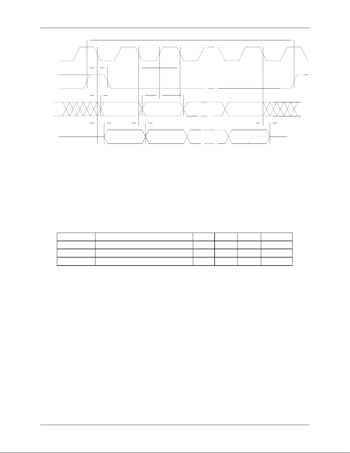
Figure 31: Timing Relation s hips with Various TTS, TCS, TPOL, and RTS, RCS, RPOL Settings
Figur e 32: Li ne -Side Device AC and DC Circuit s
Figure 33: DC-IV Char acterist ics
Figure 34: Tip-Ring Voltage versus C urrent Using Different D CIV Settings
Figure 35: Voltage versu s Current in the Seize Mode is the Same for All DCIV Set tings
Figure 36: M agnitud e R espons e of Impedance Matc hing Filt er , ACZ (3:0)=001 0 (ES 203 021-2)
Figure 37: M agnitud e R espons e of Billin g Tone Notc h Filter
Figure 38: Trans-hybrid Cancellation
Figure 39: Loopback M odes Highlighted
Figure 40: Vari ation of Transmit Gain Digital Input to Analog Output at the Line
Figure 41: Gain versus Frequency for Digital Input to Analog Output at the Line
Figure 42: Signal to Total Distortion versus Input Level for Digital Input to Analog Output to the Line
Figure 43: Vari ation of Receiver Analog Gain at the Line to the Dig i tal DX Out put
Figure 44: Gain versus Frequency for Analog Input at the Line to the Digital DX Output
Figure 45: Signal to Total D istortion versus Input Level for Anal og at the Line to the Digital D X Output
Figure 46: Return Loss, @ 80 mA
Figur e 47: 20-Pin TSSOP Package Dimensions
Figur e 48: 32-Pin QFN Package Dimen sions
Figur e 49: 42-Pin QFN Package Dimensions
.............................................................................................. 8
................................................................................................ 9
................................................................................................ 10
.................................................................................................. 12
........................................................................................................ 14
................................................................................................................ 18
..... 19
..... 20
....................................................... 21
............................................................. 21
.............................................................................. 28
.............................................................................. 29
......................................... 31
.................................................................................................... 34
.......................................................................................... 34
....................................................................................... 35
..................................................................................... 35
..................................................................................... 35
.................................................................................................. 45
................................................................................................ 46
................................................................................. 46
....................................... 46
.................................................................................. 48
.................................................................................. 48
.............................................. 49
....................................................... 50
................................................................. 51
................................................................. 51
............ 59
.................................................................................... 63
............................................................................................................ 64
............................................. 65
......................... 66
........... 67
.................................................................. 67
..................................................................................................... 68
................................................................................................ 78
..................................... 80
..................................... 81
...... 81
.................................. 82
......................... 83
... 83
.......................................................................................................... 84
..................................................................................... 85
......................................................................................... 85
......................................................................................... 86
4 Rev. 1.6

DS_1x66B_001 73M1866B/73M1966B Data Sheet
Tables
Table 1: 73M1906B 20-Pin TSSOP Pin Definitions .................................................................................. 8
Table 2: 73M1916 20-Pin TSSOP Pin Definition s
Table 3: 73M1906B 32-Pin QFN Pin Definitions
Table 4: 73M1916 32-Pin QFN Pin Definitions
Table 5: 73M1866B Pin Definitions
Table 6: Isolation Barr i er Characteristics
Table 7: Absolute Maximum Device Ratings
Table 8: Recommended Operating Conditions
Table 9: DC Char acteristics
Table 10: SPI Inter fac e Switc hing Characteristics
Table 11: Swit ching Character istics – PCM Int er fac e ( Slave M ode)
Table 12: Swit ching Character istics – PCM Int er fac e ( Master M ode)
Table 13: Refer ence Voltage Specificat i ons
Table 14: Component Val ues for the Speak er D r iver
Table 15: Call Progress Monitor Specification
Table 16: Line-Side Absolute Maximum Ratings
Table 17: VBG Specifications
Table 18: Maximum DC Transmit Levels
Table 19: Transmit Path
Table 20: Recei ve Path
Table 21: Transmit Hybrid Cancellation Characteristics
Table 22: Recei ve Notch Filter
Table 23: Over-voltage D etector
Table 24: Over-current Detector
Table 25: Und er -v oltage Detector
Table 26: Over-load Detec tor
Table 27: Refer ence Bil l of Materials for 73M1x66B
Table 28: Refer ence Bil l of Materials for Figure 14
Table 29: Compatible Pulse Transformer Sources
Table 30: Pulse Transformer Electrical C haracteristics
Table 31: Con trol and Status Register M ap
Table 32: Al phabeti cal Bit M ap
Table 33: PC M C ontrol Functions
Table 34: Transmit Gain Contr ol
Table 35: Recommended Gain Setting
Table 36: Recei ve Gain Control
Table 37: Barr ier Control Functions
Table 38: DA A C ontrol Functions
Table 39: Recommended Regi st er Settings for International Compatibi lity
Table 4 0: Li ne Sensing Control F unctions
Table 41: Loopback M odes
Table 42: Loopback M odes Summ ar y
Table 43: Order Numbers and Pac kaging M ar ks
..................................................................................... 9
..................................................................................... 10
....................................................................................... 12
........................................................................................................ 14
................................................................................................ 16
.......................................................................................... 16
....................................................................................... 16
................................................................................................................... 17
.................................................................................. 18
........................................................ 19
...................................................... 19
........................................................................................... 20
.............................................................................. 21
........................................................................................ 22
.................................................................................... 22
................................................................................................................ 23
................................................................................................ 23
......................................................................................................................... 24
......................................................................................................................... 25
.......................................................................... 26
............................................................................................................... 26
............................................................................................................ 27
............................................................................................................. 27
.......................................................................................................... 27
................................................................................................................. 27
............................................................................... 30
................................................................................. 31
................................................................................. 32
........................................................................... 32
............................................................................................ 37
.............................................................................................................. 38
.......................................................................................................... 52
............................................................................................................ 57
................................................................................................... 57
............................................................................................................. 59
........................................................................................................ 61
........................................................................................................... 68
............................................. 72
.............................................................................................. 75
.................................................................................................................... 78
.................................................................................................... 79
.................................................................................... 87
Rev. 1.6 5
73 M1 866B/73M1966B D ata Sheet DS_1x66B_001
PRM SCM
(LSBI)
SinC3
Filter
On-Chip
LIC
(OnLIC)
SPI
Interface
PCM
Interface
Interpolation
Filter
Filter
PCM
SPI
Tip
Ring
PRP SCP
Host -Side Device
73M1906B
Line-Side Device
73M1916
Aux A/D
TxA
RxA
Off-Chip
LIC
(OffLIC)
(HSBI)
Decimation
Transmit
Receive
Host
Interface
Side
Barrier
Interface
Side
Barrier
Line
Digital
Sigma
Delta
Modulator
Transmit
Analog
Front End
Receive
Analog
Front End
(with Sigma
Delta
Modulator)
Call Progress Monitor Audio Out
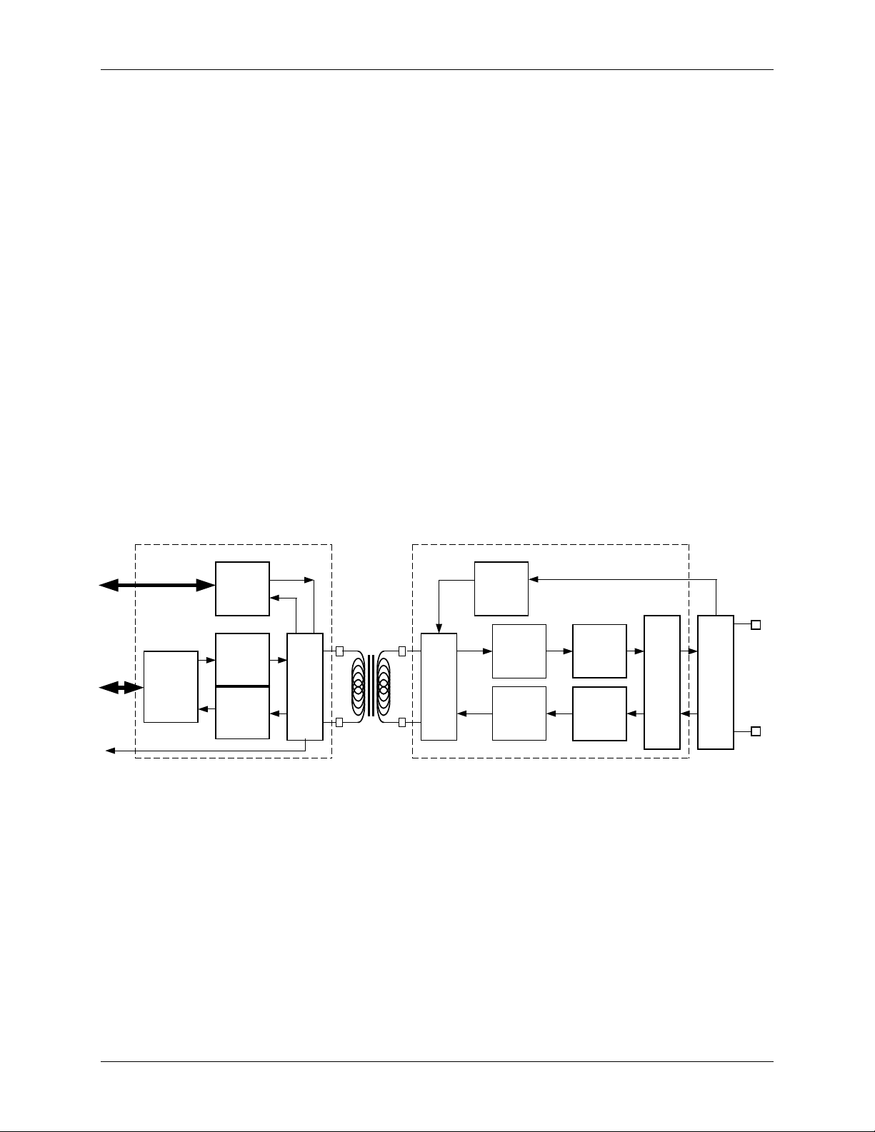
1 Introduction
The 73M1966B is a two-device chip set that provides embedded FXO functionality by connecting a PCM
interface to a voice-band PSTN. The device set supports ITU-T Rec omm endat ion G.711 µ-law and A-law
companding, and als o a 16-bit linear mode. High-voltage isolation is provided by the physical separation
of the H ost-Side (73M19106) and Line-Side (73M1916) Devices. The Host-Side and the Li ne -Side
Devices communicate with each other using a single pu l se trans former. A few low-cost components
complete the DAA interface to the network. The pulse transformer tr ansmi ts encoded digital data rather
than analog signals as with other transformer designs. Data is transmi tted and received without the usu al
deg r adation from common mode noise and magneti c coupling typic al of other capacitive an d voice-band
tran sformer techniques. The data str eam passed between the Host -Side and Line-Side Devices includes
the m edia stream dat a, control, status, and cl ocking informati on.
This data sheet describes both the 73M19 66B and 73M 1866B, which will be collectively referred to as the
73M1x66B in this document.
A un i que capability of the 73M1x66B Host Side device (73M1906B) is its ability to provide power to the
73M1x66B Line Side device (73M1916) via the pulse transformer.
The 73M1906B exchanges control and status information with the host us in g the SPI interface, while the
PCM encoded media streams connect with other PC M-enabled devices using the PCM highway bus
interface.
Figure 1 shows a referenc e block diagram of the 73M1x66B connected by a pulse transform er and
example external lin e i nterface circu itry shown for clarification.
The Host-Side Device (73M1906B) consists of:
1. PCM Interface Bloc k (PCM)
2. SPI Inter face Bloc k (SPI)
3. Transmit Interpolation Filter
4. Receive Decimati on Filt er
5. Host-Side Barrier I nterface Circui t (HSBI)
6 Rev. 1.6
Figure 1: Simple 73M1x66B Reference Block Diagram

DS_1x66B_001 73M1866B/73M1966B Data Sheet
The Line-Side Device (73M1916) consist s of:
1. Di gital Sigma Delta Modulator
2. Transmit Analog Front End
3. Receive Analog Front End including Sigma Delta Modulator
3
4. Sinc
Filter (Sinc3)
5. On-chip Line Interface Circuit
6. Line-Side Barrier Interface Cir cuit (LSBI)
Received data from a h ost connected to the PCM bus is interpolated from the s am pling frequency of
8 kH z or 16 kHz (for PCM encoded str eams) to twice the sampling frequency. The control information is
multiplexed with th e audio stream sig nals and transmi tted across the isolation barrier to the Li ne-Side
Device. In the Line-Side Device, the t wo stream s are separated and the audio signal is convert ed to
analog for transmission t o the line.
An audio stream received at the analog line inpu t pins is c onverted to a seriali zed data stream and, along
with s tatus information such as line condit ion from the Auxiliar y Analog to Digital Converter, is transmitted
over the isolation barrier using th e pulse tr ansformer. The dat a i s extracted with status informat ion being
tran smitted on the SPI. The audio stream is sent to a host using the PC M bus.
The 73M1x66B is an enhanced version of the 73M1966 that includes the additional functionality of finer
resolution of t r ansmi t and receive gain, receiver DC offset sub traction and support for T-1 PCLK
frequencies.
Rev. 1.6 7
73 M1 866B/73M1966B D ata Sheet DS_1x66B_001
73M1906B
1
2
3
4
5
6
7
8
9
10 11
12
13
14
15
16
17
18
19
20
CS
VPD
DR
DX
FS
PCLKO
PCLKI
VNA/VND
AOUT
VPA VNT
SCLK
SDI
SDIT
SDO
RST
PRM
PRP
VPT
INT
20
SCLK
I
SPI clock
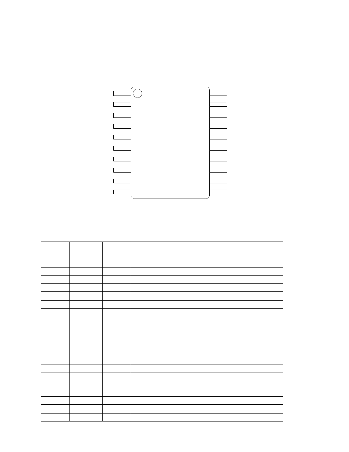
2 Pinout
The 73M1906B and the 73M1916 are supplied as 20-pin TSSOP packages and as 32 -pin QFN packages.
2.1 73M1906 B 20-Pin TSSOP Pinout
Figure 2 shows t he 73M1906B 20-pin TSSOP pinout.
Figure 2: 73M1906B 20-Pin TSSOP Pinout
Table 1 describes the pin functions for th e device. Dec oupling capacitors on the power supplies should
be included for each pair of supply pins.
Table 1: 73M1906B 20-Pin TSSOP Pin Definitions
Pin
Number
1
Pin
Name
CS
Type Description
I SPI chip selec t (active low)
2 VPD PWRI Positive digital supply
3 DR I PCM transmit data sen t to the D to A
4 DX O PCM received data from the A to D
5
FS
I/O PCM frame synchronization
6 PCLKO O PCM clock output
7 PCLKI I PCM clock in
8 VNA/VND GND Negative analog/digital ground
9 AOUT O Aud i o output – must be buffered for speaker
10 VPA PWRI Positive anal og supply
11 VNT GND Negative transformer supply
12 PRM I/O Transformer pr imary minus
13 PRP I/O Transformer pr imary plus
14 VPT PWRI Positive tr ansformer supply
15
RST
16 SDIT O S PI data out for dais y c hain mode
17 SDI I SPI data in
18 SDO O SPI data out
19
INT
I Hardw ar e reset (active low)
O Interrupt / ring detect (active low – open drain)
8 Rev. 1.6

DS_1x66B_001 73M1866B/73M1966B Data Sheet
73M1916
1
2
3
4
5
6
7
8
9
10 11
12
13
14
15
16
17
18
19
20
DCI
RGN
RGP
OFH
VNX
SCP
MID
VPX
SRE
SRB VBG
DCS
DCD
TXM
RXM
RXP
ACS
VNS
VPS
DCG
8
VPX
PWR
Sup ply from the barrier
11
VBG
O
VBG bypass, connect to 0.1 μF capacitor to VNS
2.2 73M1916 20-Pin TSSOP Pinout
Figure 3 shows the 73M1916 20-pin TSS O P pi no u t.
Figure 3: 73M1916 20-Pin TSSOP Pinout
Table 2 describes the pin functions for the device. Decoupling capacitors on the power supplies should
be included for each pair of supply pins.
Table 2: 73M1916 20-Pin TSSOP Pin Definitions
Pin
Number
Pin N ame Type Description
1 DCI I DC loop input
2 RGN I Ring detect neg ative voltage input
3 RGP I Ring detect positive voltage input
4 OFH O Off-hook c ontrol
5 VNX GND Negative supply voltage (line s i de of the barrier)
6 SCP I/O P ositive side of th e second ar y pulse t r ansformer winding
7 MID I/O Char ge pum p mi d po i nt
9 SRE I Voltage r egulat or sense
10 SRB O V ol tage reg ulator drive
12 ACS I A C current sense
13 VNS GND An al og negative supply voltage
14 VPS PWRO An al og positive supply voltage (output)
15 RXP I R eceive plus – signal input
16 RXM I Rec eive minus – signal input
17 TXM O Transmi t minus – transhybrid cancellation output
18 DCD O DC loop output
19 DCS I DC loop curren t sense
20 DCG O DC l oop control
Rev. 1.6 9
73 M1 866B/73M1966B D ata Sheet DS_1x66B_001
6
7
8
9
5
4
3
2
1
17
18
19
20
24
23
22
21
10
11
12
13
14
15
16
32
31
30
29
28
27
26
25
GPIO7
TSC
DX
VPD
FS
PCLKO
PCLKI
VND
SDO
SDI
SDIT
RST
VPD
VPT
PRP
PRM
VNA /
VNPLL
VBG
AOUT
VPA /
VPPLL
N/C
VNT
N/C
N/C
73M1906B
GPIO5
GPIO6
DR
VPD
CS
SCLK
INT
VND
Pin
Pin N ame
7
PCLKI
I
PCM clock in
12
VPA/VPPLL
PWR
Positive anal og/PLL supply
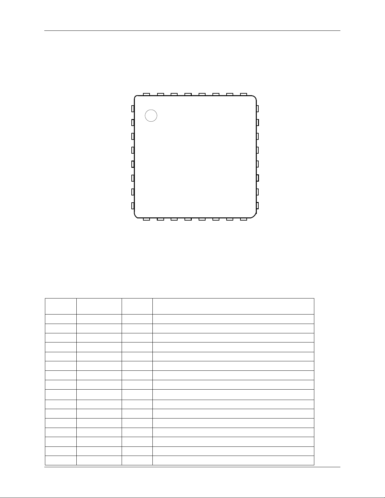
2.3 73M1906 B 32-Pin QFN Pinout
Figure 4 shows t he 73M1906B 32-pin QFN pinout.
Figure 4: 73M1906B 32-Pin QFN Pinout
Table 3 describes the pin functions for the device. Decoupling capacitors on the power supplies should
be included for each pair of supply pins.
Table 3: 73M1906B 32-Pin QFN Pin Definitions
Number
Type Description
1 GPIO7 I/O Configurable input/output pin
2 TSC O P C M time slot control ( active low)
3 DX O P C M r eceived data from the A to D
4 VPD PWR Positive digital su pply
5
6 PCLKO O PCM clock output
8 VND GND Negative digital g r ound
9 VNA/VNPLL GND Negative analog/PLL ground
10 VBG O B and gap voltage reference monitor
FS
I/O P C M frame synchroniz ation
11 AOUT O Audio output – must be buffered for speaker
13 N/C – No con nect
14 VNT GND Negative t r ansformer supply
15 N/C – No con nect
16 N/C – No con nect
10 Rev. 1.6

DS_1x66B_001 73M1866B/73M1966B Data Sheet
21
I
Hardw ar e reset (active low)
Pin
Number
17 PRM I/O Transformer pr imary minus
18 PRP I/O Transformer p r imary plus
19 VPT PWR Positive transformer suppl y
20 VPD PWR Positive digital su pply
RST
22 SDIT O S PI data out for daisy-chain mode
23 SDI I S PI data in
24 SDO O S PI data out
25 GPIO5
26 VND
27 INT
28 SCLK
29 CS
30 VPD PWR Posit ive dig ital supply
31 DR I P C M transmi t data sen t to the D to A
32 GPIO6 I/O Configurable input/output pin
Pin N ame
Type Description
I/O Configurable input/output pin
GND Negative digital ground
O Interrupt / ring detect (active low – open drain)
I SPI clock
I S PI chip s el ect (active low)
Rev. 1.6 11
73 M1 866B/73M1966B D ata Sheet DS_1x66B_001
6
7
8
9
5
4
3
2
1
17
18
19
20
24
23
22
21
10
11
12
13
14
15
16
32
31
30
29
28
27
26
25
CKO
OFH
CKI
VNX
SCP
MID
SCM
VPX
RST
DCD
TST
TXM
SACIN
RXM
RXP
VPS
RCT
BYP
SRE
SRB
VNS
VBG
ACS
VNS
73M1916
DCS
GPO
GPI
VNS/VND
RGP
RGN
DCI
DCG
Pin
Pin
9
RCT
I
External rectification – disables intern al r ectifier wh en low,
14
VBG
O
VBG bypass, connect to 0.1μF capacitor to VNS
2.4 73M1916 32-Pin QFN Pinout
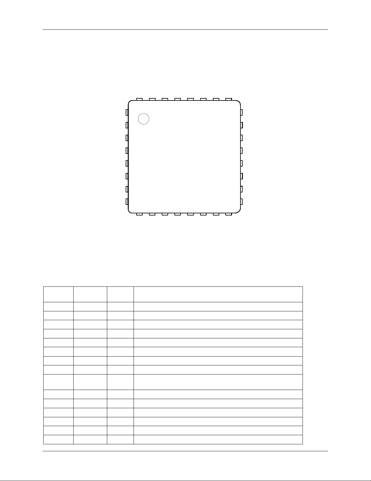
Figure 5 shows the 73M1916 32-pin QFN pi no ut.
Figure 5: 73M1916 32-Pin QFN Pinout
Table 4 describes the pin functions for the device. Decoupling capacitors on the power supplies should
be included for each pair of supply pins.
Table 4: 73M1916 32-Pin QFN Pin Definitions
Number
Name
Type Description
1 CKO O Test point for r ecovered clock
2 OFH O Off-hook control
3 CKI I Test input for clock
4 VNX GND Negative supply voltage
5 SCP I/O Positive side of the secondary pulse t r ansformer windi ng
6 MID I/O Charge pump mi d po i nt
7 SCM I/O Negative side of the second ar y pulse transformer winding
8 VPX PWR Supply from the barrier
10 BYP I Test pin, leav e open
11 SRE I Voltage regulator sense
12 SRB O Voltage regulator drive
13 VNS GND Digital negative supply voltage
leave open
15 ACS I AC current sense
12 Rev. 1.6

DS_1x66B_001 73M1866B/73M1966B Data Sheet
26
DCG
O
DC loop control
29
RGP
I
Ring detect positive voltage input
Pin
Number
Pin
Name
Description
Type
16 VNS GND An al og negative supply voltage
17 VPS PWRO Analog positive supply voltage (output)
18 RXP I Receive plus – signal i nput
19 RXM I Receive minus – signal input
20 SACIN I Call er ID mode AC impedanc e connecti on
21 TXM O Transmit Minus – trans hybrid cancellati on output
22
23
TST
RST
I Factory test mode, leave open
I Resets the control registers to default – weakly pulled high
24 DCD O DC loop output
25 DCS I DC loop current sense
27 DCI I DC loop input
28 RGN I Ring detect negati ve voltage input
30 VNS GND Negative supply voltage (line s i de of the barrier)
31 GPI I General purpos e input ( test pin)
32 GPO O General purpose output (test pin)
Rev. 1.6 13
73 M1 866B/73M1966B D ata Sheet DS_1x66B_001
DX
VPD
FS
PCLKO
VNA
PCLKI
AOUT
VPA
VNT
PRM
PRP
VPT
RST
SDIT
SDI
VND
SDO
INT
SCLK
CS
DR
SRE
SRB
VBG
ACS
VNS
VPS
RXM
RXP
TXM
DCD
DCS
DCG
DCI
RGN
RGP
OFH
M20PB
VNX
SCP
MID
VPX
73M1866B
1
2
3
4
5
6
7
8
9
10
20
11
12
13
14
15
16
17
18
19
21
22
23
24
25
26
27
28
29
30
31
32
33
35
34
36
37
38
39
40
41
42
Pin
1
O
PCM received data from the A to D
8
PWR
Positive anal og supply
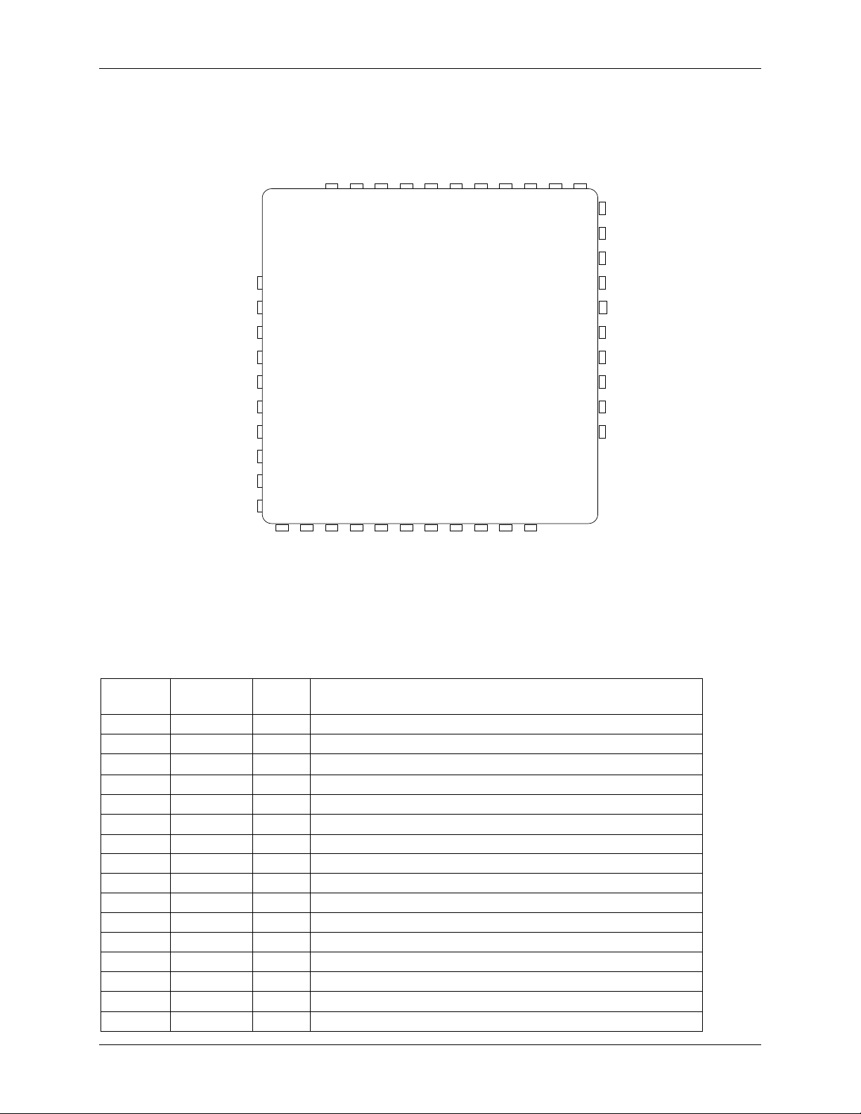
2.5 73M1866 B Pinout
Figure 6 shows t he 73M18 66B 42-pin pinout.
Figure 6: 73M1866B 42-Pin Pinout
Table 5 describes the pin functions for the device. Decoupling capacitors on the power supplies should
be included for each pair of supply pins.
Table 5: 73M1866B Pin Definit ions
Number
2 VPD PWR Positive digital supply
3
4 PCLKO O PCM clock output
5 VNA GND Negativ e analog ground
6 PCLKI I PCM clock in
7 AOUT O A udio out put – must be buffered for speaker
9
10
11 PRP I/O Transform er primary plu s
12 VPT PWR Positive transfor mer su pply
13
14 SDIT O SPI data out for d ai sy-chain mode
15 SDI I SPI dat a in
16 SDO O SPI data out
14 Rev. 1.6
Pin N ame Type Description
DX
FS
VPA
VNT
PRM
RST
I/O PCM frame synchron ization
GND Negative transformer supply
I/O Tr ansformer primary minus
I Hardware reset (active low)

DS_1x66B_001 73M1866B/73M1966B Data Sheet
31
O
DC loop output
41
I/O
Char ge pum p mi d po i nt
Pin
Number
Pin N ame Type
Description
17 VND GND Negative digital g r ound
18 INT O Interrupt / ring detect (active low – open drain)
19
SCLK
I SPI clock
20 CS I SPI chip sel ect (act i ve low)
21
22
DR
SRE I Voltag e r egulat or sense
23 SRB
24
VBG
25 ACS
26
27
28
29
30
VNS
VPS PWRO Analog positive supply voltage (output)
RXP
RXM
TXM
DCD
I PCM transmit data sent to the D to A
O Voltage regulator drive
O VBG bypass, connect to 0.1μF capacitor to VNS
I AC current sense
GND A nalog negative supply voltage
I Receive pl us – signal inp ut
I Receive m inus – s ignal inp ut
O Transmit Minus
– transhybri d cancellation output
32 DCS I DC l oop current sense
33
34
35
36
37
38
39
DCG
DCI
RGN
RGP
OFH
M20PB
VNX
O DC loop contr ol
I DC loop input
I Ring detect negative voltage input
I Ring detect positive voltage input
O Off-h ook con trol
I Test pin . Connect to VNX.
GND Negative supply voltage
40 SCP I/O Positive si de of the secondary pulse trans former winding
MID
42
VPX
PWR Supply from the bar r i er
2.6 Requisite Use of Expos ed Bottom Pa d o n 73M1866 B and 73M1966B QFN Packages
The exp osed bottom pad is not intended for t hermal r elief (heat diss i pation ) and should not be
sold er ed to the PCB. Soldering of the expos ed pad could also comprom i se electrical
isolation/insulation requir ements for proper voltage isolation. Avoid any PCB traces or through -hole
vias on the PCB beneath the exposed pad area.
Rev. 1.6 15
73 M1 866B/73M1966B D ata Sheet DS_1x66B_001
Parameter
Rating
Parameter
Min
Max
Unit
Parameter
Min
Max
Unit
3 Electrical Characteristics and Specifications
3.1 Isolation Barrier Characteristics
Table 6 provides the character istics of the 73M1x66B Isolati on Barrier.
Table 6: Isolation Barrier Characteristics
Barrier frequ en cy 768 kHz
Data t r ansfer rate across the barrier for the sampling r ate of 8 kHz 1.536 Mbps
When 16 kHz sampling rate is selec ted, the frequency and data transfer rates are twic e those shown
above.
3.2 Electrical Specif ic ati ons
This s ection provides t he absolute m aximum ratings, the recomm ended oper ating conditions and the DC
characteristics.
3.2.1 Absolute Maximum Ratings
Table 7 l i sts the maximum operating condition s for the 73M1x66B. Perman ent device d amage may occ ur
if absol ute m aximum ratings are exceeded. Exposure to the extremes of the abs olut e m aximum rating for
extended peri ods may af fect devi ce reliability.
Table 7: Absolute Maximum Device Ratings
Sup ply voltage -0.5 4.0 V
Pin input voltage (except OSCIN) -0.5 6.0 V
Pin input voltage (OSCIN) -0.5 to VDD 0.5 V
3.2.2 Recommended Operating Conditions
Function operation should be restri cted t o the recommended op er ating conditions speci fied in Table 8.
Table 8: Recommended Operating Conditions
Sup ply voltage (VDD) wit h respect to VSS 3.0 3.6 V
Operating temperature -40 85 °C
16 Rev. 1.6

DS_1x66B_001 73M1866B/73M1966B Data Sheet
Parameter
Condition
Min
Nom
Max
Unit
–
–
–
–
–
–
–
–
–
–
–
–
–
–
–
–
–
–
–
–
–
–
–
–
–
3.2.3 DC Characteristics
Table 9 lists the 73M1x66B DC chara cte ristics.
Table 9: DC Characteristics
Input low voltage VIL – -0.5 –
Input high voltage VIH1 – 0.7 VDD
Output low voltage VOL IOL=4 mA
Output low voltage
VOL IOL= 1 mA
FSB,SCLK,
Output high voltage VOH IOH=-4 mA VDD - 0.45
Output high voltage
VOH IOH=-1 mA VDD - 0.45
FSB, FSBD, SCLK
Input low leakage current IIL1 VSS < Vin < VIL1 10
Input high l eakage
IIH1 VIH1 < Vin < 5.5 –
current
IDD curr en t at 3.0 V – 3.6 V Nominal at 3.3 V
Active digital current IDD1
Active PLL current IDD1
Active analog current IDD1
IDD total current* IDD1
IDD total current* IDD2
IDD cu rrent
IDD3
dig
pll
ana
1.0 1.5 mA
1.0 1.5 mA
12 17 mA
15 20 mA
20 30 mA
1.0 5 μA
PWDN=1
IDD cu rrent
IDD4
0.5 1.0 mA
SLEEP=1 (Ext Ref Clk)
IDD cu rrent
IDD6
1.0 1.5 mA
ENFEH=0 (Ext Ref Clk)
0.2 ∗ VDD
5.5 V
0.45 V
0.45 V
V
V
40 μA
1 μA
V
*Note: IDD1 is with the secondary of the barrier left open.
IDD2 is with the secondary of the barrier connected to 73M1916 fully powered.
Rev. 1.6 17
73 M1 866B/73M1966B D ata Sheet DS_1x66B_001
–
–
–
–
–
–
–
–
–
–
–
–
–
–
SDO turn off delay
t
– – 20
ns
SDO hold time
t
– – 20
ns
CS
SCLK
SDI
SDO
t
ics
t
scy
t
ids
t
idh
t
odd
t
odh
t
odo
t
ich
3.3 Interface Timing Specification
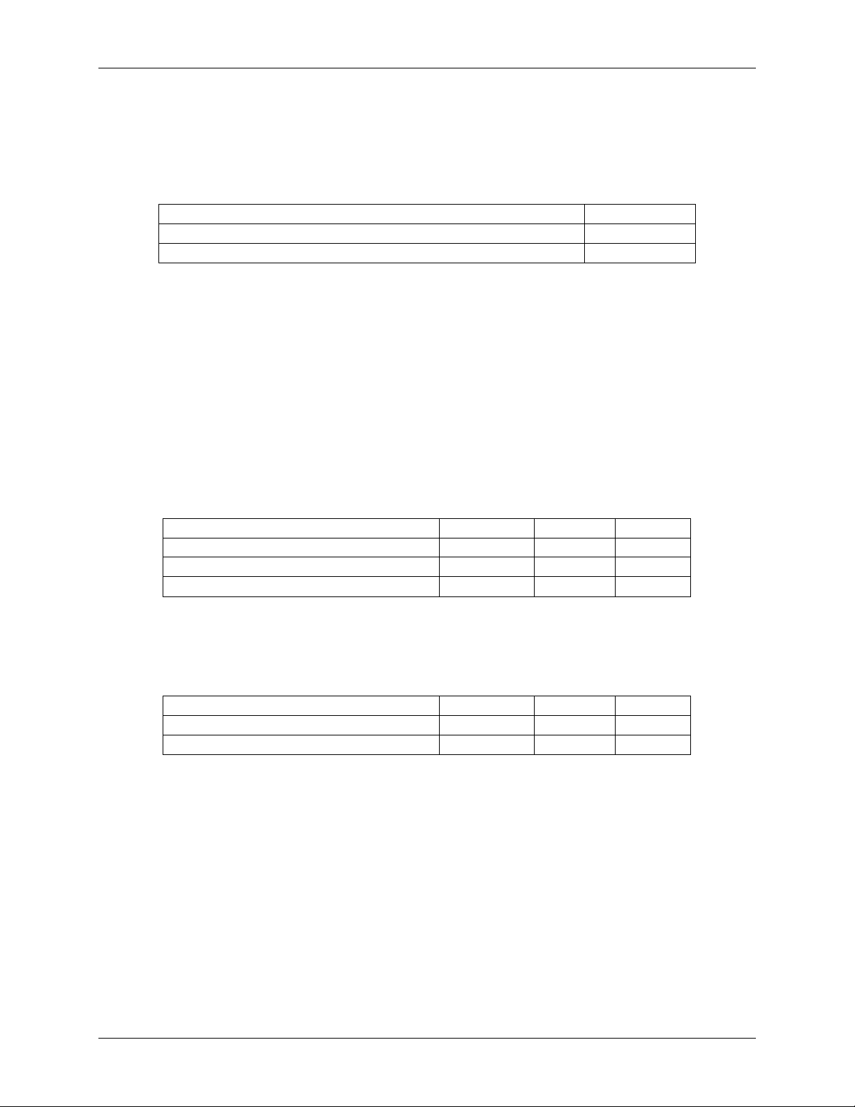
There ar e three interfaces assoc iated with the 73M1x66B: th e SPI interfac e, the PCM highway interface
and the line interface. This sec tion p r ovides the timi ng specific ation for the SPI interfac e and the PCM
highway interface.
3.3.1 SPI Interface
Table 10 li sts the character i stics for the SPI interfac e.
Table 10: SPI Interface Switching Characteristics
Parameter Symbol Min Typ Max Unit
SCLK cycle time1 t
SCLK rise tim e t
SCLK fall time t
CS setup time t
CS hold time t
SDI setup time t
SDI hold time t
SDO turn on d el ay t
SDI to SDITHRU propagation del ay t
Note1: The minimal value of this paramet er is for the case where only one 73M1906B is connect ed to the
host. If the daisy chai n mode is used, th e m inimum S CL K cycle time increas es according t o the numb er
of slaves in t he chain.
62.5
scy
scr
scf
25
ics
20
ich
25
ids
20
idh
–
odd
odo
odh
– 6 – ns
idt
– ns
25 ns
25 ns
20 ns
ns
ns
ns
ns
18 Rev. 1.6
Figure 7: SPI Timing Diagram
DS_1x66B_001 73M1866B/73M1966B Data Sheet
Parameter
Symbol
Min
Typ
Max
Unit
pcy
–
–
–
–
–
–
–
–
–
–
ids
–
–
idh
–
–
odd
–
–
odo
–
–
–
–
Parameter
Symbol
Min
Typ
Max
Unit
PCLK_OUT cycle time
t
–
488 – ns
–
–
–
–
–
–
–
–
–
–
–
–
–
DX tu r n on delay
t
–
–
20
ns
DX turn off delay
t
–
–
20
ns
–
–
FS
PCLK
DR
DX
t
ifs
t
pcy
t
ids
t
idh
t
ird
t
odd
t
odo
t
ifh
t
ifc
t
odh
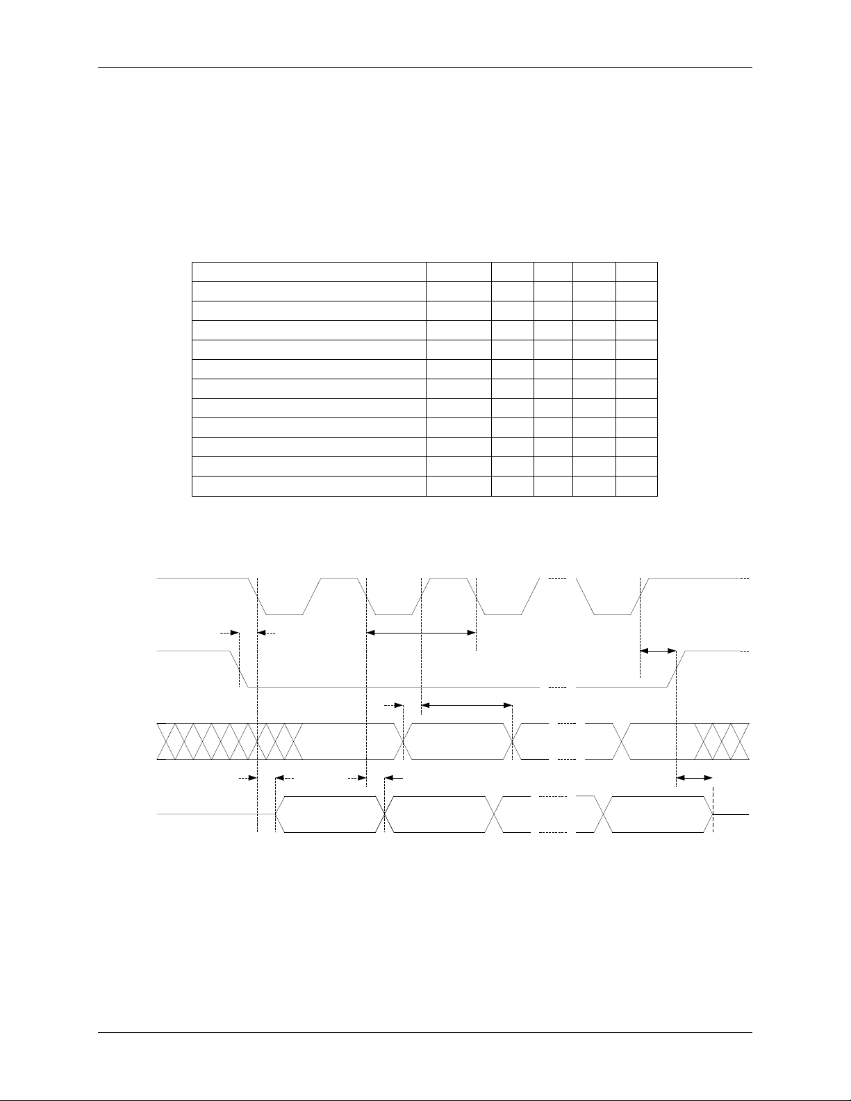
3.3.2 PCM Highway Interface
Table 11: Switching Characteristics – PCM Interface (Slave Mode)
PCLK_IN cycle time t
PCLK_IN rise tim e t
PCLK_IN fall time t
FS s etup tim e t
FS hold time t
FS cycle time t
DR setup tim e t
DR hold time t
DX tu r n on delay t
DX turn off delay t
DX hold time t
122
pcr
pcf
25
ifs
20
ifh
– 125
ifc
25
20
odh
3906 ns
25 ns
25 ns
ns
ns
μs
ns
ns
20 ns
20 ns
20 ns
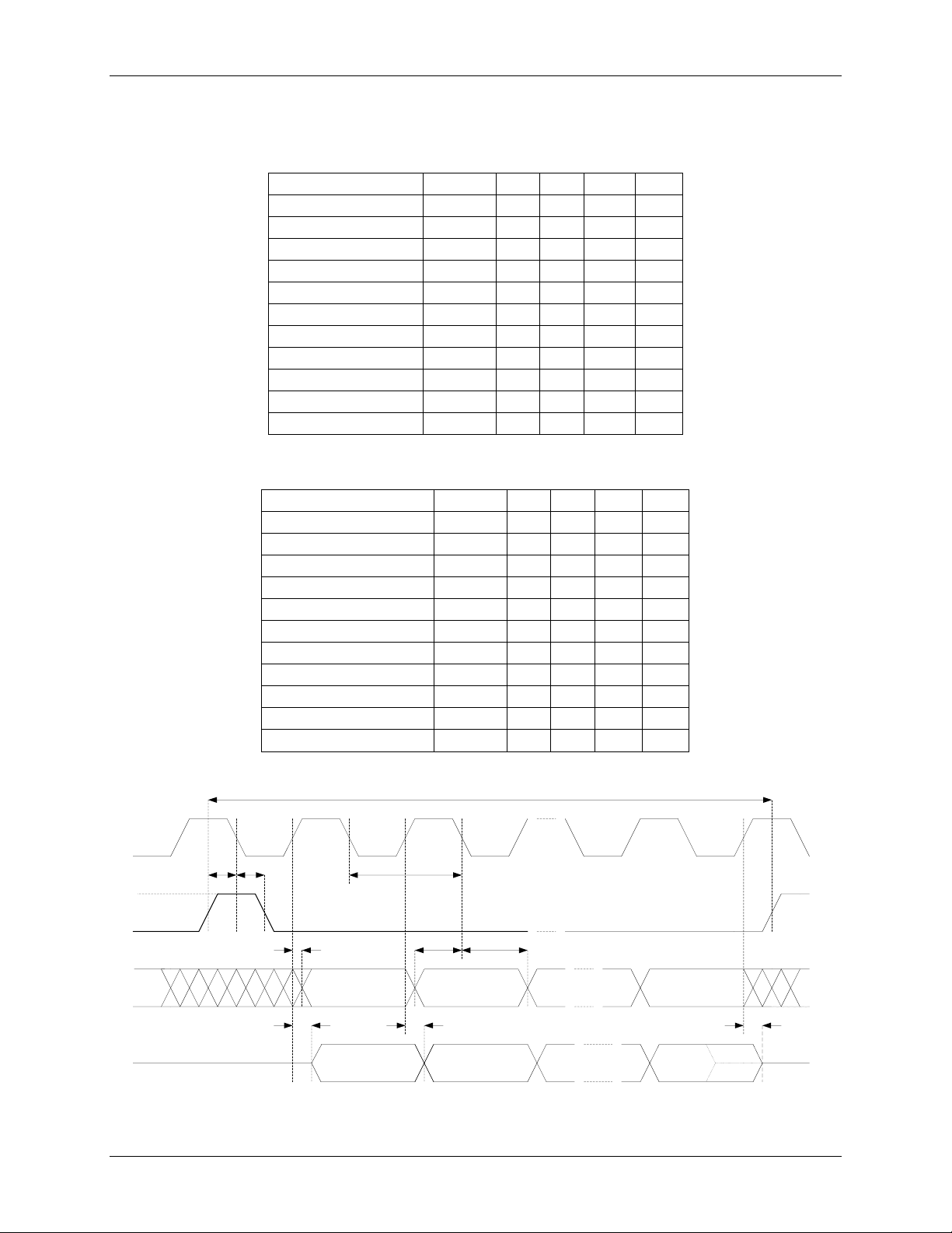
Table 12: Switching Characteristics – PCM Interface (Master Mode)
pcy
PCLK_OUT rise tim e t
PCLK_OUT fall time t
FS s etup tim e t
FS hold time t
FS cycle time t
DR setup tim e t
DR hold time t
DX hold time t
pcr
pcf
50
ifs
50
ifh
– 125
ifc
25
ids
20
idh
odd
odo
odh
25 ns
25 ns
ns
ns
μs
ns
ns
20 ns
Figure 8: PCM Timing Diagram for Positive E dg e T ran smit Mode and Neg at ive Edg e R ec eiv e Mo de
Rev. 1.6 19
73 M1 866B/73M1966B D ata Sheet DS_1x66B_001
FS
PCLK
DR
DX
t
ifs
t
pcy
t
ids
t
idh
t
ird
t
odd
t
odo
t
ifh
t
odh
Figure 9: PCM Timing Diagram for Negative Edge Transmit Mode and Positive Edge Receive Mode
3.4 Analog Specifications
This s ection provides t he electrical characteri zations of the 73M1x66B analog circui try.
3.4.1 DC Sp ecifications
VBG i s to be connected to an external bypass c apacitor with a minimum value of 0.1 μF. This pin is not
intended for any other external use.
Table 13: Reference Voltage Specifications
Parameter Te st Condition Min Nom Max Units
VBG VDD=3.0 V – 3.6 V 0.9 1.19 1.4 V
VBG Noise 300 Hz – 3.3 kHz – -86 -80 dBm
600
VBG PSRR 300 Hz – 30 kHz 40 – – dB
20 Rev. 1.6
DS_1x66B_001 73M1866B/73M1966B Data Sheet
U1 NJM2135
CD
1
-VIN
4
V+
6
GND
7
VOUT1
5
VOUT2
8
VREF1
2
VREF2
3
AOUT
VCC
VCC
R3 120K
+
C2
2.2uF
LS1
INTERVOX
AT-2308
C4
1uF
R2 120KR1 120K
C3
1uF
C1 0.1uF
Quantity
Reference
Part Description
Part
3.4.2 Call Progress Monitor
The Call Progress Monitor monitors activities on the line. The audio output contains both transmit and
receive data with a configurable level individually set by Register 10h.
Figure 10 shows the frequency response of the Call Progress Monitor Filter b ased upon the
characteristics of the devic e plus the external c ircuitry as shown.
Figure 10: Frequency Response of the Call Progress Monitor Filter
Figure 11: Demo Board Circuit Connecting AOUT to a Speaker
Table 14: Component Values for the Speaker Driver
1 C1 Ceramic cap acitor 0.1 μF
1 C2 Ceramic cap acitor 2.2 μF (optional)
2 C3 , C4 C er amic capacitor 1 μF
1 LS1 Sound transducer Speaker (Intervox)
3 R1 , R2 , R3 1/8 W resistor 0603 120 kΩ
1 U1 Audio amplifier NJM2135 (N ew Japan Radio)
All measurements are at the AO UT pin with CMVSEL= 0. Note that when CMVSEL=1, the peak signal at
AOU T is increas ed to approximately 1.11 Vpk.
Rev. 1.6 21
73 M1 866B/73M1966B D ata Sheet DS_1x66B_001
Parameter
Test Condition
Min
Nom
Max
Units
– – –
–
AOUT transm it THD
CMTXG=00
–
40 – dB
– – –
–
CMRXG=00
–
0.96
–
Vpk
–
–
–
–
–
–
–
–
–
–
Table 15: Call Progress Monitor Specification
AOUT for transmit
AOU T for receiv e
AOU T rec eive THD CMRXG=00
AOUT output
impedance
1 kHz full swing code (ATX)
CMRXG=11 (Mute)
Observe AOUT pi n
CMTXG=00 – 0.98 – Vpk
CMTXG=01 relat i v e
to CMTXG=00
CMTXG=10 relat i ve
to CMTXG=00
CMTXG=11 (Mute) – Mute – dB
1.0 Vpk, 1 kHz at the line or 0.5
Vpk at RXP/RXM with
RXG=10
CMTXG=11 (Mute)
Observe AOUT pi n
CMRXG=01 relative
to CMRXG=00
CMRXG=10 relative
to CMRXG=00
CMRXG=11 (Mute)
– -6 – dB
– -12 – dB
-6
-12
Mute
40
10
3.5 73M1x66 B Lin e-Side Electrical Specifications (73M1916)
dB
dB
dB
dB
kΩ
Table 16 li sts the absolute maximum r ating s for the li ne side. Operation outside these rating limits may
cause permanent damage to this device.
22 Rev. 1.6
Table 16: Line-Side Absolute Maximum Ratings
Parameter Min Max Unit
Pin input voltage from VPX to V NX -0.5 6.0 V
Pin input voltage (all ot her pins) to V N S -0.5 4.0 V
DS_1x66B_001 73M1866B/73M1966B Data Sheet
Parameter
Test Condition
Min
Nom
Max
Units
VBG noise
300 Hz – 3.3 kHz
–
-86*
-80
dBm
VBG PSRR
300 Hz – 30 kHz
40 – –
dB
DCIV=01
0.83
0.92
1.00
V
DCIV=10
1.08
1.16
1.24
V
*Noise
–
3.6 Reference and Regulation
Table 17 list s the VBG specifications. V BG shou ld be connected to an external bypass capacit or with a
minimum value of 0.1 μF. This pin is not intended for any other external use.
The following conditions apply: VPX=5 V; Barri er Powered Mode; Barrier Data Rate across the
Barrier=1.5 Mbps; VBG connected to 0.1 μF extern al cap.
Table 17: VBG Specifications
VBG See condit ions above. – 1.19 – V
600
VPS VPX=5.5 V – 3.15 – V
VPS PSRR VPX=4.5 V to 5.5 V – 40 – dB
3.7 DC Transfer Characteristics
Table 18 list s the maximum DC transmit levels. All tests are driven at pin DCI and measured at pin DCS.
DCEN=1. ILM=1.
Table 18: Maximu m DC Tr an smit Lev el s
Parameter Test Condition Min Nom Max Units
V
DCON
(DC "On" Voltage)
With ENAC=0 DCIV=XX 0.20 0.26 0.30 V
DC Gain V
I
bef or e ILIM ILM=1 V
DCI
I
after ILIM ILM=1 V
DCI
Delta V
Delta I
DCS
DCI
DCIV=00 0.62 0.69 0.78 V
DCIV=11 1.32 1.42 1.53 V
DCON<VDCI
8.2∗45mA< V
At the line with 300 Ω(ac) (0.15 - 4.0 kHz )
<0.4V+V
=0.28V+V
DCI
=0.44V+V
DCI
DCS
< 8.2∗60mA
-0.30 0 .0 +0.25 dB
DCON
DCON
DCON
– – 10 µA
20 – – µA
– 0.85 – mA/V
-85 -80 dBm
Rev. 1.6 23

73 M1 866B/73M1966B D ata Sheet DS_1x66B_001
–
–
–
–
–
–
ACZ=0001
–
0.211
–
Vpk
ACZ=0010
–
0.211
–
Vpk
–
–
–
–
–
–
–
–
–
–
–
–
–
–
ACZ=1010
–
0.223
–
Vpk
ACZ=1011
–
0.313
–
Vpk
–
–
–
–
–
–
–
–
–
–
–
–
Passband ripple
150 Hz – 3.3 kHz
-0.125
–
+0.125
dB
– – –
–
–
– 0 –
–
–
–
–
–
–
3.8 T r ansm it Pat h
Table 19 li st th e transmi t path characteristi cs. A pattern for a s inusoid of 1 kH z, full scal e ( code word of
+/- 32,767) from the 73M1x66B is forced and ACS is measured with R10=174 Ω. Unless stated
otherwise, test conditions are: ACZ=0000 (600 Ω termination), THEN=1, ATEN=1, DAA=01, TXBST=0,
sample rate=8kHz.
Table 19: Transmit Path
Parameter Test Condition Min Nom Max Units
Offset volt age
8 an d 16 kHz samp le rate
Tx gain, relative to
DAA[1:0]=01
AC swing
(1 kHz sinusoid)
8 an d 16 kHz samp le rate
50% 1’s density relative to 1.4
V common mode.
DAA=00 2.5 +3 3.5 dB
DAA=01 -0.5 0 0.5 dB
DAA=10 -4.5 -4 -3.5 dB
DAA=11 -8.5 -8 -7.5 dB
DAA=01
DAA=00
TXBST=1, DAA=xx
– 25 – mV
0.317
0.447
0.634
Vpk
Vpk
Vpk
ACZ=0011
ACZ=0100
ACZ=0101
ACZ=0110
ACZ=0111
ACZ=1000
ACZ=1001
ACZ=1100
ACZ=1101
ACZ=1110
ACZ=1111
Idle noise 300 Hz – 4 kHz
THD 300 Hz – 4 kHz
Intermod distort i on
1.0 kHz and 1.2 kHz
summed
Aliased image Fs +/- 1 kHz, relati ve t o 1 kHz
300 Hz – 4 kHz – -85 – dB
Gain relative to 1 kHz
0.5 kHz
1.0 kHz
2.0 kHz
3.3 kHz
0.200
0.254
0.220
0.171
0.194
0.222
0.205
0.208
0.211
0.285
0.235
-80
-80
0.17
0.193
-0.12
-75
Vpk
Vpk
Vpk
Vpk
Vpk
Vpk
Vpk
Vpk
Vpk
Vpk
Vpk
dBm
dB
dB
dB
dB
dB
dB
dB
24 Rev. 1.6

DS_1x66B_001 73M1866B/73M1966B Data Sheet
Parameter
Test Condition
Min
Nom
Max
Units
Intermod Dist 1.0 kH z
3.9 Rec ei v e Pat h
Table 20 li sts the receive pat h characteristics. All test inputs are driven through an AC coupling net work
shown in Figure 29. The receive bit stream is measu r ed at the DX pin. RXE N=1.
Table 20: R eceive Path
Differential input
resistance
Input level Differential, RX P/RXM – 1.1 1.16 Vpk
Input level Common mode, R XP/RXM – 1.37 – V
Overall sigma-delta A DC
modulation gain inclusive
of 73M1906B processing
Offset voltage R6=17.4 kΩ, R8=52.3 kΩ,
Rx gain
(See Note 1.)
Overal l r eceive
frequ ency response
inclusive of 73M1906B
processing
Idle noise 300 Hz – 4 kHz – -80 – dBm
THD RXG=00 – -85 – dB
Normalized t o VBG=1.19 V.
RXP/RXM – 1000 – kΩ
RXG=00
Divide Vrxp/m by PCM
Output
R9=21 kΩ.
See Figure 12.
RXG=00 -0.5 0 0.5 dB
RXG=01 2.5 3 3.5 dB
RXG=10 5.5 6 6.5 dB
RXG=11 8.5 9 9.5 dB
RXBST=1, RXG=00 18.3 19.3 20.3 dB
Relative to 1 kHz
0.3 kHz – 3.3 kHz -0.25 0 +0.25 dB
Fs (8 kHz) – -75 – dB
RXBST=1 – -60 –
– 47.3 – µV/bit
– 0 +/- 30 mV
– – –
–
and 1.2 kHz sum med
Crosstalk 1 Vpk 1 kHz sine wave at
CMRR RXP=RXM 1 Vpk 40 – – dB
PSRR -30 dBm signal at VPX in
On-Hook AC Impedance 300 Hz – 4 kHz, without EMI
Note 1: RXG controls the amount of gain or attenuation of the receiver analog gain element as specifi ed
in Table 20. The overall r eceiver c hann el gain has 6 dB of attenuat ion and th e net effect of t he
RXG bits on the receiver c hannel gain is defined i n Table 36.
Rev. 1.6 25
300 Hz – 4 kHz – -85 – dB
TXP; FFT on Rx ADC
samples, fir st four harmoni cs
reflec ted to the lin e.
Barrier Powered Mode;
300 Hz – 30 kHz.
caps.
– -90 – dBm
– – 40* dB
– 2 – MΩ
73 M1 866B/73M1966B D ata Sheet DS_1x66B_001
Parameter
Test Condition
Min
Nom
Max
Units
RLPNH=0 (12 kHz Notch)
–
–
–
–
–
–
–
Pass band Ripple (0. 3 kHz – 3.4 kHz)
–
+/- 0.15
–
dB
– 28.8 – μs
–
–
–
–
–
–
–
–
RLPNH=1 (16 kHz Notch)
–
–
–
–
3 kHz
–
+0.11
–
dB
16 kHz
-30
-50 – dB
–
–
–
–
–
–
–
–
–
–
–
3.10 Transmit Hybrid Cancellation
Table 21 li sts the transmit hybrid cancellation characterist ics. Un less stated otherwise, test conditi ons
are: ACZ[3:0]=0000 (600 Ω termination), THEN=1, ATEN=1, DAA[1:0]=01, TXBST=0. TXM is externally
fed back into the 73M1916 to effect cancellation of transmit signal.
Table 21: Transmit Hybrid Cancellation Characteristics
Transmit hybrid cancellation Measure in
73M1906B
Offset volt ag e 50% 1’s dens i ty – 0 25 mV
AC swing 1 kHz sinusoid 1.00 1.05 1.10 Vpk
Idle noise 300 Hz – 4 kHz – -80 – dBm
– 20 – dB
3.11 Receive Notch Filter
Table 22 li sts the receive not ch filter charact eristics. A ll measurements taken with RLPNEN=1, TXEN= 0,
RXG=00, ATEN=1. RXP is driven with 1 Vpk signal.
Table 22: Receive Notch Filter
Parameter Test Condition Min Nom Max Unit
Magnitude respons e
Delay
300 Hz
1 kHz
3 kHz
12 kHz -30 -50
300 Hz
1 kHz
3 kHz
12 kHz
0.0
+0.03
+0.04
28.93
30.25
41.62
9.95
dB
dB
dB
dB
μs
μs
μs
μs
Magnitude respons e
Delay
26 Rev. 1.6
300 Hz
1 kHz
Pass band Ripple (0. 3 kHz – 3.4 kHz)
300 Hz
1 kHz
3 kHz
16 kHz
0.0
+0.04
+/- 0.15
30.53
30.66
31.93
42.26
4.74 – μs
dB
dB
dB
μs
μs
μs
μs

DS_1x66B_001 73M1866B/73M1966B Data Sheet
Parameter
Test Condition
Min
Nom
Max
Unit
3.12 Detectors
This s ection provides electrical charac teristics fo r the foll owing detector s:
• Over-Voltage.
• Over-Current.
• Under-Voltage.
• Over-Load.
3.12.1 Over-Voltage Detector
The values in Table 23 were measured between RGP and RG N .
Table 23: Over-voltage Detector
Parameter Test Condition Min Nom Max Unit
Over voltage levels OVDTH=0 0.52 0.6 0.68 V
OVDTH=1 0.59 0.7 0.77 V
3.12.2 Over-Current Detector
The values in Table 24 were measured in Barrier Powered Mode.
Table 24: Over-current Detector
Parameter Test Condition Min Nom Max Unit
Over current level Meas ured at DCS. 0.90 1.025 1.20 V
3.12.3 Under-Voltage Detector
The values in Table 25 were measured in Barrier Powered Mode. In the recommended schemati c (see
Figure 12), disconnect Q5 collector and connect to an exter nal power supply, VPE, through a 600 Ω
resistor.
Table 25: Under-voltage Detector
Parameter Test Condition Min Nom Max Unit
Under voltage detect Measure VPE when UVD is
detected as VPE is dec r eased.
– 7.5 – V
3.12.4 Over-Load Detector
The values in Table 26 were measured in Barrier Powered Mode.
Table 26: Over-load Detector
Over l oad level Measu r ed at DCI with 1 k H z. 0.6 0.75 0.9 Vpk
Rev. 1.6 27

R69
100K*
C14
15pF
INT\
SCLK
C41
220pF, 300V
SDO
SDI
VCC
SDITHRU
+
C8
4.7uF
R2
10M, 0805
R12 5.1K
R11
3K
C39
5.6nF
Q7
MMBTA42
1
3
2
R68
1M, 0805
C3 0.022uF, 200V
RST\
C48
0.1uF
Q6
BCP-56
1
23
4
DR
VPS
C49
100pF
C1 0.022uF, 200V
R8
52.3K, 1%
R9
21K, 1%
R5 8.2, 0805
R3
412K, 1%
U1 73M1916-20
OFH
4
VNX
5
SCP
6
MID
7
VPX
8
VBG
11
ACS
12
SRE
9
SRB
10
VNS
13
VPS
14
RXP
15
RXM
16
TXM
17
DCS
19
DCD
18
DCI
1
RGN
2
RGP
3
DCG
20
R6
17.4K, 1%
R66
1M, 0805
C38
0.1uF
C12
0.1uF
R4
100K, 1%
C7
4.7uF, 25V
U2 73M1906B-20
CS
1
AOUT
9
VPD
2
VPT
14
PCLKO
6
PCLKI
7
SCLK
20
DX
4
DR
3
FS
5
SDIT
16
SDO
18
SDI
17
VPA
10
VNA/VND
8
PRM
12
PRP
13
RST
15
VNT
11
INT
19
DX
AUDIO
C33
1nF
FSIO
IS OL ATION BARRIER
C31
0.1uF
CLKO
C35
220pF, 3KV
CLKI
-+
BR1
HD04
4
1
3
2
C36
220pF, 3KV
C37
0.01uF
TP15
VPS
1
TP14
OFH
1
R58 240
L1
2K Ohms @ 100 MHz
C9
0.22uF
T1
1 4
2 3
F1
TRF600-150
L2
2K Ohms @ 100 MHz
C10
0.22uF
TISP4290T3BJ
R10
174, 1%
Q3
MMBTA42
1
32
R65 200
Q4
MMBTA92
1
3 2
E1
P3100SBRP
Q5
MMBTA06
1
32
C24
NC (TBD as needed, 3KV)
C13
15pF
C26
1nF
CS\
SRE
SRB
C20
1nF
SCP
C43
1nF
NOTE: GND for C35 and
C36 should be on the host
side of the barrier
+
C4
10uF
VCC
C30
1nF
+
C21
3.3uF
C17
0.1uF
+
C45
3.3uF
VCC
TIP
RING
D1
MMSZ4710T1*
73 M1 866B/73M1966B D ata Sheet DS_1x66B_001
4 Applications Information
This s ection provides general u sage information for th e design and implement ation of the 73M1x66B.
4.1 Exa mple Schematic of the 73M1966B and 73M1866 B
Figure 12 shows a typical application schemat i c for the implementation of the 73M1966B. Figure 13 shows a typical application schematic for the
implement ation of the 73M1866B. Note that min or changes m ay oc cur to the reference material from tim e to time and the reader is encouraged to
contact Teridian for t he latest inform ation. For more information about schematic and layout design, s ee the 73M 1 86 6B/73M 19 6 6B S c hematic an d
Layout Guidelines.
28 Rev. 1.6
Figure 12: Recommended Circuit for the 73 M1 9 66B

DS_1x66B_001 73 M1 866B/73M1966B D ata Sheet
R6
17.4K, 1%
T1
Pulse Transf ormer
1
4
2 3
C1
0.022uF, 200V
C3
0.022uF, 200V
C43
1nF
C49
100pF
C35
220pF, 3k V
C30
1nF
R5
8.2
C33
1nF
R3 412K, 1%
R66
1M, 0805
VNS
VCC
C37
0.01uF
M aintain 2.5 mm Spacing Between
Line and Host Side Components
Isolation Bar r ier
C38
0.1uF
F1
TRF600-150
E1
P3100SBRP
C20
1nF
U1
73M1866B
DX
1
VPD
2
FS3PCLKO
4
VNA5PCLKI
6
AOUT
7
VPA8VNT
9
PRM
10
PRP
11
VPT
12
RST
13
SDIT
14
SDI
15
SDO
16
VND
17
INT
18
SCLK
19
CS
20
DR
21
SRE22SRB23VBG24ACS25VNS
26
VPS
27
RXP
28
RXM
29
TXM
30
DCD
31
DCS
32
DCG
33
DCI
34
RGN
35
RGP
36
OFH
37
M20PB
38
VNX
39
SCP
40
MID
41
VPX
42
RSTB
C26
1nF
SDITHRU
SPI OUT
SPI IN
SPI CLK
C39
5.6nF
C36
220pF, 3k V
VNS
SPI CSB
C9
0.22uF
PC M TX
C41
220pF, 300V
INTB
R11
3K
VCCVCCVCC
R68
1M, 0805
C17
0.1uF
PCM CLKIN
C13
15pF
C12
0.1uF
L1 2 k Ohm @100MHz
PCM CLKO
C14
15pF
VNS
VNS
AOUT
R2
10M
+
C45
3.3uF
+
C21
3.3uF
+
C8
4.7uF
RING
TIP
R12
5.1K
-+
BR1
HD04
4
1
3
2
R58 240
R9
21K, 1%
Q3
MMBTA42
1
32
Q6
BCP56
1
23
4
L2 2 k Ohm @100MHz
Q4
MMBTA92
1
3 2
R10
174, 1%
R4
100K, 1%
Q5
MMBTA06
1
3
2
PCM FS
C10
0.22uF
Q7
MMBTA42
1
32
C7
4.7uF, 25V
PCM RX
R65
200
NOTE: GND for C35 and C36 should be on
the host side of the barrier
C31
0.1uF
C48
0.1uF
R8
52.3K, 1%
C24
NC (as needed, 3KV)
+
C4
10uF
D1
MMSZ4710T1*
R69
100K*
Rev. 1.6 29
Figure 13: Recommended Circuit for the 73M1866B

73 M1 866B/73M1966B D ata Sheet DS_1x66B_001
1
R2
10 M , 5%, 1/8W r esistor 0805
Yageo
RC0805JR-0710ML
1
R3
412 K, 1%, 1/10W resistor 0603
Yageo
RC0603FR-07412KL
1
R12
5.1 K, 5%, 1/10W resistor 0603
Yageo
RC0603JR-075K1L
1
R58
240 , 5%, 1/10W r esistor 0603
Yageo
RC0603JR-07240RL
4.2 Bill of Materials
Table 27 provides the 73M1x66 bill of materials for the reference schematics provided in Figure 12 and
Figure 13.
Table 27: Reference Bill of Materials for 73M1x66B
Qty Reference Part Description Source Example MFR P/N
1 BR1 HD04 rectifier bridge, 0.8A, 400V Diodes Inc. HD04-T
2 C1, C3 0.022μF 200V, X7R, 1206 Panasonic ECJ-3FB2D223K
1 C4 10μF 6.3V, tantalum, 0805 AVX, Panasonic TCP0J106M8RA
1 C7 4.7μF 25V, X5R, 0805 AVX, Panasonic 08053D475KAT2A
1 C8 4.7uF 6.3V, tantalum, 0805 Rohm TCP0J475M8R
2 C9, C10 0.22μF 16V, X7R, ceramic, 0603 Panasonic C0603C224K8RACTU
C12,C17,C31,
4
C38, C48
2 C13, C14 15pF 50V, ceramic, 0603 Panasonic ECJ-1VC1H150J
C20, C26, C30,
5
C33, C43
2 C21, C45 3.3μF 6.3V, tantalum, 0805 Rohm TCP0J335M8R
1 C37 0.01μF 50V, X7R, ceramic, 0603 AVX, Panasonic 06035C103KAT2A
1 C39 5.6nF 50V, X7R, ±10% ceramic, 0603 Panasonic ECJ-1VB1H562K
1 C49 100pF 50V, ceramic, 0603 Taiyo Yuden UMK107CH101JZ-T
1 D1 25V, 500mW Zener diode ON Semi MMSZ4710T1,
1 Q5
1 Q4
2 Q3 , Q7
1 Q6 NPN 80 V transistor SOT223 Fairchild, On Semi BCP56
0.1μF 16V, X7R, ceramic, 0603
1nF 10V, X7R, ceramic, 0603 Panasonic C0603C102K8RACTU
MMBTA06, NPN 80 V tra ns istor
SOT23
MMBTA92, PNP 300 V transistor
SOT23
MMBTA42, NPN 300 V transistor
SOT23
Pan asonic, Kemet C0603C104K8RACTU
Diodes, Fairchild,
Central, On Semi
Diodes, Fairchild,
Central, On Semi
Diodes, Fairchild,
Central, On Semi
MMBTA06LT1G
MMBTA92LT1G
MMBTA42LT1G
1 R4 100K, 1%, 1/ 10 W resistor 0603 Yageo RC0603FR-07100KL
1 R5 8.2, 5%, 1/8W resistor 0805 Yageo RC0805JR-078R2L
1 R6 17. 4K , 1% , 1/ 10W resis to r 060 3 Yageo RC0603FR-0717K4L
1 R8 52. 3K , 1% , 1/ 10W resis to r 060 3 Yageo RC0603FR-0752K3L
1 R9 21K, 1%, 1/10W res i stor 0603 Yageo RC0603FR-0721KL
1 R10 1 74, 1%, 1/10W resis tor 0603 Yageo RC0603FR-07174RL
1 R11 3 K, 5%, 1/10W resistor 060 3 Yageo RC0603JR-073K0L
1 R65 2 00, 5%, 1/10W resis tor 0603 Yageo RC0603JR-07200RL
2 R66, R68 1 M, 5%, 1/8W resistor 0805 Yageo RC0603JR-071ML
1 R69* 100K typ. 5% , 1/10W resistor 0603 Yageo RC0603JR-07100KL
1 T1 Pu l se trans former See Table 29.
* Optional – see the 73M1866B/1966B Sc hematics an d Layout Gui d el i n es for details .
30 Rev. 1.6

DS_1x66B_001 73 M1 866B/73M1966B D ata Sheet
C35
220pF, 3k V
C36
220pF, 3k V
L1
2K Ohm @ 100MHz
F1
TR600-150
L2
2K Ohm @ 100MHz
J1
RJ-11
1
2
3
4
5
6
E1
P3100SBRP
or equiv.
T
R
C41
220pF, 300V
4.3 Over-Voltage and EMI Protection
Over-voltage prot ection i s requi r ed to meet worst-case c ondit i ons for target cou ntries. UL195 0,
EN60950, IEC 60950, ITU-T K.20/ K.21 and GR-1089-CORE s pecifications define the protec tion
requirements for many coun tries. A s ingle design can be implemented to meet all thes e r equirements .
Figure 14 shows a r ecommended pr otection circuit topology. Fus e ( F1) shou l d be rated ap propriately for
the country of operation, and the bidirectional th yristor (E1) should have a min imum break-over of 220 V,
a maximum br eak-over of 275 V and be able to survive a 10 0 A fast tr ansient. In addition to over-voltage
and current protection, the 73M1x66B sh ould make p r ovisions t o prevent EMI emissions and EMC
suscept ibilit y. Figure 14 also illustrates how L1, L2, C35, C36 and C41can provide this suppression. The
ferrite beads , L1 and L2, should be capable of passing 150 mA and have an impedance of 2K Ω at 100
MHz. C 35, C36 an d C41 shoul d be between 47pF and 220nF, and rated for a breakdown voltage greater
than the hig hest isolation voltage or line voltage that is requ ired for cou ntry compatibi l ity. C35 and C36
should be returned to an earth ground. EMI suppression is highly dependent on the physical design of
the overall circ uit an d not all the suppression components may be needed in every design and
application.
Figure 14: Suggested Over-Voltage Protection and EMI Suppression Circuit
Table 28: Reference Bill of Materials for Figure 14
Reference Part Description Source Example MFR P/N
E1 Bidirectional Thyristor Diodes Inc., Bourns
TB3100H-13-H,
TISP4290T3BJR-S
F1 PPTC Fuse Tyco, Bourn s MF-R015/600 or equiv.
L1,L2 2 KΩ @ 100 MHz, 150 mA min, 0805 Steward, TDK MPZ2012S601A
C35, C36 220 pF, 3000 V TDK C4532COG3F221K
C41 220 pF, 30 0 V Vishay VJ1206Y221KXEAT5Z
Rev. 1.6 31

73 M1 866B/73M1966B D ata Sheet DS_1x66B_001
4.4 Isol at i on Bar r i er Pul s e Tr an sf ormer
The isolation el ement used by the 73M1 x66B is a standard digital pul se trans former. Several ven dors
supply compatibl e transformers with up to 6000 V rating s. Since the tran sformer is the only component
crossing the isolation barrier other th an EMI capacit or s that may be r equired, it s olely determines the
isolat ion bet ween th e PSTN and the FXO’s digit al interface. This method of isol ation is signi fi cantly
superior to ot her isolation tec hniques with major advantages in high common mode voltage operation,
lower radiated noise (EMI) and improved operation in noisy environments. Table 29 lists some pulse
transformers compatible with the 73M1x66B. The t able also includes low-voltage transformers that offer
low-cost alternatives if such voltages are sufficient.
Table 29: Compatible Pulse Transformer Sources
Company Number
Sumida ESMIT 4180
ESM IT 4181
Wurth Electronics Midcom Inc. 750110001
UMEC TG-UTB01543S
Datatronics PT79280
AAsupreme P950003
Table 30 li sts some of the t ypical pulse transformer specifications used by the 73M1x66B. Contact the
manufacturer directl y for product informati on.
Table 30: Pulse Transformer Electrical Characteristics
Parameter Test Condition Min Nom Max Tolerance Unit
Inductance 100 kHz, 10 mVA C, 1-2, Ls. 54 60 200 – μH
Interwinding
Capacitance
Turn Ratio – – 1:1 – ±2 % N/A
DC Resistance Primary – – 0.25 – Ω
Dielectric Breakdown
Voltage
ET Constant – – 1.2 – – Vμs
Su r ge Test 1.2 x 50 μs 2800 6000 – V
Oper ating Temperature – -40 – 85 –
– – – 6 – pF
Secondary – – 0.25 – Ω
1 sec 2000 3750 – – Vrms
°C
32 Rev. 1.6

DS_1x66B_001 73 M1 866B/73M1966B D ata Sheet
Bit 7
Bit 6
Bit 5
Bit 4
Bit 3
Bit 2
Bit 1
Bit 0
BRCT
R/W X X
CID[0]
CID[1]
CID[2]
CID[3]
5 SPI Interface
The hos t access es the 73M1x66B using an SPI interface to write to control registers and read statu s
registers. Th e host is the master of the transaction. Four pins orchestr ate the c ommunicat ion between
the host and the SPI, and a fifth pin is dedicated to support the daisy-chain mod e. The signals are as
follows:
• SDI Serial data input driven by the host.
• SDO Serial data output driven by the 73M1x66B.
• SCLK Clock input driven by the host.
• CS Chip select inp ut driven by t he host.
• SDIT Serial data output for d aisy-chai n mod e.
The SPI implemented by the 73M1x66B has the following key features:
• Sup port for 8-bit and 16-bit mode operations.
• Sup port for daisy-chain operations.
• Sup port for both cont inuously active S C LK or SCLK active during t r ansfers on l y.
• Sup port for br oadcast mode.
Transaction s between the hos t and the 73M1x66B requir e three bytes. All bytes are transmitted most
sig nificant byte firs t. The first is the contr ol byte, the second the address byte an d the third is the data
byte. The cont r ol byte is s tructured as follows:
The value of CID[0:3] determines which 73M1x66B in the daisy chain should execute the read or write
operation requested by the host. Up to 16 devices in the daisy chain can be supported. The daisy chain
organization is shown in Figure 15. The control byte is subm i tted to the first 73M1x66B in the daisy
chai n. If th e value of CID[0:3] is different from zero, the SPI of that device decreases the value of
CID[0:3] by one and passes the new value through SDIT to the next 73M1x66B in the chain. This
process continues until CID[0:3] is zero, thus stopping at the device designated to execute the operation.
The value of CID will be the position in the daisy chain for the device being addressed minus one.
If the host is controll ing only one 73M1x66B, CID[0:3] must be set to 0.
The BRCT bit ov er r ides the chip address ing driven by CID[0:3]. The host asserts BRCT for all write
operat ions that must be execut ed by all 73M1x66B devices in th e chain. At t hat time, whatever comes in
SDI comes out through SD IT. BRCT does not affect read operations.
Rev. 1.6 33

73 M1 866B/73M1966B D ata Sheet DS_1x66B_001
HOST
73M1906B
Channel 0
73M1906B
Channel 1
73M1906B
Channel 15
...
SCLK
SCLK
SCLK
SCLK
CS
CS
CS
SDO
SDO
SDO
SDO
CS
SDI
SDI
SDI
SDI
SDITHRU
SDITHRU
SDITHRU
CID=CIDin-1
CID=CIDin-2
CIDin
CID=000
(target)
CONTROL ADDRESS DATA [7:0]
SCLK
SDI
SDO
HI-Z
CS
Figure 15: Daisy-Chain Configuration
The R/W bit d etermines wh ether the host requests a read (1 ) or a write (0) op er atio n.
The second byt e of the SPI transaction is the address byte. The address byte simply contains the 8-bit
value for the r egister targeted by the operation. For th e 73M1x66B, only six bits of t he add r ess are
relevant for the regis ter spac e, and the two most-sign i fi cant bits of the address b yt e ar e always set to 0 .
The third byte of the SPI t r ansacti on is the data byte. It contai ns the dat a to write t o the addressed
73 M1 x66B registers or the dat a r ead from t he addressed 73M1x66B register.
In the 8-bit mode, the thr ee bytes are exchang ed over three fram es, as directed by CS. Figure 16 and
Figure 17 show a write and read transaction between the 73M1x66B and the host in 8-bit mode.
Figure 16: SPI Write Operation – 8-bit Mode
34 Rev. 1.6

DS_1x66B_001 73 M1 866B/73M1966B D ata Sheet
CS
SCLK
SDO
HI-Z
DATA [7:0]
CONTROL ADDRESS DATA [7:0]
SDI
CONTROL
CS
SCLK
SDI
SDO
HI-Z
ADDRESS
DATA[7:0] XXXXXXXX
CONTROL
CS
SCLK
SDI
SDO
HI-Z
ADDRESS XXXXXXXX XXXXXXXX
DATA[15:8] DATA[7:0]
Figure 17: SPI Read Transaction – 8-bit Mode
In 16-bit mode, the first frame of 16 bits contains both the control and addr ess bytes, and the s econd
frame contain s the data bytes. Note that the second part of the second frame is irrele vant. Figure 18 and
Figure 19 sh ow the write and read transac tions in 16-bit mode.
Figure 18: SPI Writ e Tr ansactio n – 16-bit Mode
Figure 19: SPI Read Transaction – 16-bit Mode
The transaction diagrams sh ow the case where SCL K is onl y ac tive duri ng the transacti on frames. The
same transac tion remains valid even if SCLK run s continuously, regardles s of frame boundaries.
The SPI state machine resets wh en the host sends a frame containing a number of SCLK periods
different from a multiple of eight:
Rev. 1.6 35

73 M1 866B/73M1966B D ata Sheet DS_1x66B_001
• In 8-bit mode, if either the control or the address frames do n ot correspond to a multiple of eight
SCLK cycles, the SPI state mac hine resets and the transaction i s aborted. If the data frame is shorter
than eight SC LK cycles, the state machine resets and the transaction is abor ted. If the data frame i s
longer than eight SC LK cycles, while not being a multip l e of ei ght cycles, the write/read transaction is
perfo r med an d the stat e machin e r esets.
• In 16-bit mode, if the control/address frame does not con tain a multiple of eight S CL K cycles, the SPI
state mach ine resets and the t r ansact i on is abor ted. If the data fram e i s short er than eig ht SCLK
cycles, the state machine resets and the transaction is aborted. If the d ata frame is longer than eight
SCLK cycles, while not being a mult iple of eight cycles, the write/read transaction is per formed and
the state machine res ets. This schem e can be used to reset the SPI if one looses trac k of frames .
36 Rev. 1.6

DS_1x66B_001 73 M1 866B/73M1966B D ata Sheet
6 Control and Status Registers
Table 31 shows the 73M1x66B register map of address able registers. The shad ed cells in dicate read-only
bits and cannot be modified. Reserved bi ts should be left in their default state. Accessing unspeci fied
registers should be avoided. Each register and bit is described in detail in the following sections.
For registers 0x12 through 0x1F, which are located in the Line-Side D evice, ther e is a minimum time
between consecutive write transacti ons of 300 µs when using an 8 kHz sample rate.
Table 31: Control and Status Register Map
Address
(hex)
Default Bit 7 Bit 6 Bit 5 Bit 4 Bit 3 Bit 2 Bit 1 Bit 0
02 10h TMEN
03 E0h GPIO7 GPIO6 GPIO5 PCLKDT RGMON DET SYNL RGDT
04 E4h DIR7 DIR6 DIR5 Reserved REVHSD3 REVHSD2 REVHSD1 REVHSD0
05 1Bh ENGPIO7 ENGPIO6 ENGPIO5 ENPCLKDT ENAPOL ENDET ENSYNL ENRGDT
06 00h POL7 POL6 POL5 Reserved Reserved Reserved Reserved Reserved
07 00h Reserved Reserved Reserved Reserved Reserved Reserved DTST1 DTST0
08 00h TXDG -12 TXDG -6 TXDG +3.5 TXDG +2 TXDG +1 TXDG +0.5 TXDG +0.25 TXDG +0.125
09 00h RXDG -12 RXDG -6 RXDG +3.5 RXDG +2 RXDG +1 RXDG +0.5 RXDG +0.25 RXDG +0.125
0D 40h LOKDET SLHS Reserved Reserved
0E 00h FRCVCO Reserved Reserved Reserved Reserved Reserved RGTH1 RGTH0
0F 80h ENFEH PWDN SLEEP Reserved Reserved Reserved Reserved Reserved
10 00h Reserved Reserved Reserved CMVSEL CMTXG1 CMTXG0 CMRXG1 CMRXG0
12 00h OFH ENDC ENAC ENSHL
13 00h DCIV1 DCIV0 ILM Reserved PLDM OVDTH IDISPD SEL16K
14 00h TXBST DAA1 DAA0 Reserved RXBST RLPNH RXG1 RXG0
15 00h ENOLD DISNTR Reserved CIDM THEN ENUVD ENOVD ENOID
16 00h TXEN RXEN RLPNEN ATEN ACZ3 ACZ2 ACZ1 ACZ0
17 00h Reserved Reserved RXOCEN Reserved Reserved Reserved Reserved Reserved
18 01h TEST3 TEST2 TEST1 TEST0 Reserved Reserved Reserved Reserved
19 00h POLL MATCH Reserved Reserved INDX3 INDX2 INDX1 INDX0
1A 00h RNG7 RNG6 RNG5 RNG4 RNG3 RNG2 RNG1 RNG0
1B 00h LV7 LV6 LV5 LV4 LV3 LV2 LV1 Reserved
1C 00h LC6 LC5 LC4 LC3 LC2 LC1 LC0 Reserved
1D 00h REVLSD3 REVLSD2 REVLSD1 REVLSD0 Reserved Reserved Reserved Reserved
1E 00h ILMON UVDET OVDET OIDET OLDET SLLS Reserved Reserved
1F 00h POLVAL7 POLVAL6 POLVAL5 POLVAL4 POLVAL3 POLVAL2 POLVAL1 POLVAL0
20 00h TPOL TTS6 TTS5 TTS4 TTS3 TTS2 TTS1 TTS0
21 00h RPOL RTS6 RTS5 RTS4 RTS3 RTS2 RTS1 RTS0
22 00h SR ADJ RCS2 RCS1 RCS0 TCS2 TCS1 TCS0
23 00h PCMEN MASTER PCODE3 PCODE2 PCODE1 PCODE0 LIN LAW
24 00h Reserved Reserved Reserved Reserved Reserved Reserved Reserved LB
25 00h RXOM7 RXOM6 RXOM5 RXOM4 RXOM3 RXOM2 RXOM1 RXOM0
Reserved Reserved
Reserved Reserved ENLPW Reserved Reserved
RSTLSBI
ENLVD
Reserved Reserved Reserved
ENFEL ENDT ENNOM
Rev. 1.6 37

73 M1 866B/73M1966B D ata Sheet DS_1x66B_001
Bit Name
Register
Page
Default
Type
Category
LOKDET
0x0D[7]
42
0
R
Device Clock Man agemen t
Throughout this document, type W is read/write, type WO is write only and type R is read only. Registers
and bits are defined as 0x16[3:0], where 0x16 is the register addr ess and the numbers i n square bracket s
specify the address bits. The bit order is [msb – ls b] for a field . For example, [3:0] means bits 3 through 0
of a particular field.
Table 32: Alphabetical Bit Map
ACZ
ADJ
ATEN
CIDM
CMRXG1/0
CMTXG1/0
CMVSEL
DAA1/0
DCIV1/0
DET
DIR5
DIR6
DIR7
DISNTR
DTST1/0
ENAC
ENAPOL
ENDC
ENDET
ENDT
ENFEH
ENFEL
ENGPIO7
ENGPIO6
ENGPIO5
ENLPW
ENLVD
ENNOM
ENOID
ENOLD
ENOVD
ENPCLKDT
ENRGDT
ENSHL
ENSYNL
ENUVD
FRCVCO
GPIO5
GPIO6
GPIO7
IDISPD
ILM
ILMON
INDX
LAW
LB
LC
LIN
0x16[3:0]
0x22[6]
0x16[4]
0x15[4]
0x10[1:0]
0x10[3:2]
0x10[4]
0x14[6:5]
0x13[7:6]
0x03[2]
0x04[5]
0x04[6]
0x04[7]
0x15[6]
0x07[1:0]
0x12[5]
0x05[3]
0x12[6]
0x05[2]
0x12[1]
0x0F[7]
0x12[2]
0x05[7]
0x05[6]
0x05[5]
0x02[2]
0x12[3]
0x12[0]
0x15[0]
0x15[7]
0x15[1]
0x05[4]
0x05[0]
0x12[4]
0x05[1]
0x15[2]
0x0E[7]
0x03[5]
0x03[6]
0x03[7]
0x13[1]
0x13[5]
0x1E[7]
0x19[3:0]
0x23[0]
0x24[0]
0x1C[7:1]
0x23[1]
68
52
69
75
44
44
44
52
69
76
43
43
43
61
79
69
61
69
76
76
42
70
43
43
43
61
70
70
77
77
77
52
75
70
61
76
42
43
43
43
69
70
70
40
52
79
76
52
0000
0
0
0
00
00
0
00
00
0
1
1
1
0
00
0
1
0
0
0
1
0
0
0
0
0
0
0
0
0
0
1
1
0
1
0
0
1
1
1
0
0
0
0
0
0
0
0
W
W
W
W
W
W
W
WO
WO
R
W
W
W
WO
W
WO
W
WO
W
WO
W
WO
W
W
W
W
WO
WO
WO
WO
WO
W
W
WO
W
WO
W
W
W
W
WO
WO
R
W
W
W
R
R/W
DAA Control Function
PCM Control Function
DAA Control Function
DAA Control Function
Call P r ogress Monitor
Call P r ogress Monitor
Call Progress Monitor
PCM Control Function
DAA Control Function
Line Sens in g Control
GPIO Control
GPIO Control
GPIO Control
Barrier Cont r ol Func tion
Loop back Control
DAA Control Function
Barrier Cont r ol Func tion
DAA Control Function
Line Sens in g Control
Line Sens in g Control
Power Management
Current Limiting Detection Control and Status
GPIO Control
GPIO Control
GPIO Control
Barrier Cont r ol Func tion
Current Limiting Detection Control and Status
DAA Control Function
Over-Curr ent Detection C ontrol and Status
Over-Load Detection Con trol and Status
Over-Voltage Detec tion Control and Status
PCM Control Function
Ring Detection Function
Current Limiting Detection Control and Status
Barrier Cont r ol Func tion
Under-Volt age Detection Control and Status
Device Clock Man agemen t
GPIO Control
GPIO Control
GPIO Control
DAA Control Function
Current Limiting Detection Control and Status
Current Limiting Detection Control and Status
Line-Sid e Device Register Polling
PCM Control Function
Loop back Control Function
Auxiliary A/D Converter Status
PCM Control Function
38 Rev. 1.6

DS_1x66B_001 73 M1 866B/73M1966B D ata Sheet
LV
UVDET
0x1B[7:1]
0x1E[6]
76
76
0
0
R
R
Auxiliary A/D Converter Status
Under-Volt age Detection Control and Status
Bit Name Register Page Default Type Category
MASTER
MATCH
OFH
OIDET
OLDET
OVDET
OVDTH
PCLKDT
PCMEN
PCODE
PLDM
POL7
POL6
POL5
POLL
POLVAL
PWDN
RCS
REVHSD
REVLSD
RGDT
RGMON
RGTH1/0
RLPNEN
RLPNH
RNG
RPOL
RSTLSBI
RTS
RXBST
RXDG
RXEN
RXG0
RXG1
RXOCEN
RXOM
SLEEP
SLHS
SLLS
SR
SYNL
TCS
THEN
TMEN
TPOL
TEST
TTS
TXBST
TXDG
TXEN
0x23[6]
0x19[6]
0x12[7]
0x1E[4]
0x1E[3]
0x1E[5]
0x13[2]
0x03[4]
0x23[7]
0x23[5:2]
0x13[3]
0x06[7]
0x06[6]
0x06[5]
0x19[7]
0x1F[7:0]
0x0F[6]
0x22[5:3]
0x04[3:0]
0x1D[7:4]
0x03[0]
0x03[3]
0x0E[1:0]
0x16[5]
0x14[2]
0x1A[7:0]
0x21[7]
0x0D[3]
0x21[6:0]
0x14[3]
0x09[7:0]
0x16[6]
0x14[0]
0x14[1]
0x17[5]
0x25[7:0]
0x0F[5]
0x0D[6]
0x1E[2]
0x22[7]
0x03[1]
0x22[2:0]
0x15[3]
0x02[7]
0x20[7]
0x18[7:4]
0x20[6:0]
0x14[7]
0x08[7:0]
0x16[7]
52
41
70
77
77
77
77
52
52
53
70
43
43
43
40
40
42
53
41
41
78
78
75
71
71
76
53
62
53
75
54
54
54
54
54
54
42
62
62
55
62
55
71
79
55
79
55
55
56
56
0
0
0
0
0
0
0
0
0
0
0
0
0
0
0
0
0
0
0100
0
0
0
0
0
0
0
0
0
0000000
0
00000000
0
0
0
0
0
0
1
0
0
0
0
0
0
0
0
0000000
0
00000000
0
W
R
WO
R
R
R
WO
R
W
W
WO
W
W
W
W
R
W
W
R
R
R
R
W
W
W
R
W
W
W
WO
WO
WO
WO
WO
W
W
W
R
R
W
R
W
W
W
W
W
W
WO
WO
WO
PCM Control Function
Line-Sid e Device Register Polling
DAA Control Function
Over-Curr ent Detection C ontrol and Status
Over-Load Detecti on Control and Status
Over-Voltage Detec tion Control and Status
Over-Voltage Detec tion Control and Status
PCM Control Function
PCM Control Function
PCM Control Function
DAA Control Function
GPIO Control Function
GPIO Control Function
GPIO Control Function
Line-Si de Device Register Polling
Line-Sid e Device Register Polling
Power Managem ent
PCM Control Function
Device Revision
Device Revision
Ring Detection Function
Ring Detection Function
Ring Detection Function
DAA Control Function
DAA Control Function
Auxiliary A/D Converter Status
PCM Control Function
Barrier Cont r ol Func tion
PCM Control Function
PCM Cont rol Functi on
PCM Control Function
PCM Control Function
PCM Control Function
PCM Control Function
PCM Control Function
PCM Con trol Function
Power Managem ent
Barrier Cont r ol Func tion
Barrier Cont r ol Func tion
PCM Control Function
Barrier Cont r ol Func tion
PCM Control Function
DAA Control Function
Loop back Control Function
PCM Control Function
Loop back Control Function
PCM Control Function
PCM Control Function
PCM Control Function
PCM Control Function
Rev. 1.6 39

73 M1 866B/73M1966B D ata Sheet DS_1x66B_001
Function
Register
Register given by the offset address in INDX is placed in this register.
While all registers may be read or written to via an SPI operation wit hout er r or , some registers r eact
differently to read and write operation s, as follows:
• Read/Write (W) registers change in response to an SPI write transact i on and r eport their correc t
current value for a read SPI t r ansact i on.
• Read Only (R) registers do not c hange in response to an SPI write transaction but report their
correct current value for a read SPI t r ansact i on.
• Write Only (WO) register s are shadow registers to cor r esponding r egisters on the Line-Side
Device
indirectly. The true c ontents of these Line-Side reg i sters cannot be read direc tly from the shadow
registers rep r esenting them, but these Line-Side registers can be read using the polling register
described in 6.1. Certain events, such as lightning or voltage su r ges, could corr upt the c ontents
of the Line-Side registers , so to verify their contents, the polling registers (0x19 and 0x1F) must
be u sed.
(0x12-0x18) that are written to during the barrier communications, and so ar e written to
6.1 Line-Side Dev ic e R egister Pol lin g
The Regi ster Map as read from a 73M1x66B Host-S ide Device consists of two groups. The first is th e
Host-Side Device registers (0x00 through 0x10 and 0x20 through 0x24) and the second is a copy of the
Line-Si de Device registers (0x12 through 0x1F).
As an extra degree of integrity, the 73M1x66B supports the abi lity to m anually monitor the registers of its
Line-Side Device. This is achieved by using the Manual Poll Function. The Line-Side registers that c an
be p ol led are 0x12 through 0x18 (index values 0x0-0x6 respectively).
The method i s to write the offset address o f the Line-Side Device register to be r ead int o the INDX fi el d.
The value of th i s is the offset index from 0x12; that is, Register 0x12 is 0x0, 0x13 is 0x1, etc. The next
step is to set the POLL bit, which causes the device to r ead the requested regi ster from the Line-Side
Device. The valu e of the requested Line-Side Device register is written by the Line-Side Device into
POLVAL (0x1F). This value is compared with that of the Host-Sid e copy and, if they are the same, the
MATCH bit is set to 1.
The values presented at MATCH and POLVAL are valid approximately 600 μs aft er a poll r equest, and
are valid onl y after th e POLL bit has been reset b y th e H ost-Side Device.
Mnemonic
INDX 0x19[3:0] W Index
MATCH 0x19[6] R Polling Match
POLL 0x19[7] W Polling Enable
POLVAL 0x1F[7:0] R Pollin g Value
40 Rev. 1.6
Location
Type Description
Add r ess of the register to be manually polled with the results placed in
POLVAL. This address should be cleared aft er the pol l . Default = 0.
0 = No match. (Default)
1 = Thi s read-only bit indicates that there is match with the
corresponding polled register in the Host-Side Device. The result of
the pollin g funct i on can be read only after the POLL bit is reset to zero
by the 73M1x66B.
0 = P olling d i sabled. ( D efault)
1 = Manually polls the control register in the Line-Sid e D evice whose
address is given by INDX. The Poll b it remains high until the MATCH
result is available at which time it will be reset to 0 and the MATCH bit
status can b e r ead.
When 73M1x66B is polled, the content of the Line-Side Device
Default = 0. This r egister can be r ead after the POLL bi t has been
reset to zero, indicating the result is ready.

DS_1x66B_001 73 M1 866B/73M1966B D ata Sheet
Function
Register
only status bits provide the Device ID for the 73M1x66B
7 Hardware Control Functions
This section describes the 73M1x66B capabilities with respect to its configuration and hardware pin
control. These include featur es such as Device Revision, Interr upt Management , Power Management,
Clock Control, General Purp ose Input/Output (GPIO ) and control of the Cal l Progress Monitor.
7.1 Device Revision
The 73M1x66B provides the devic e r evision numb er for the Host-Side Device and the Line-Side Device.
For the 73M1x66B:
• Revision for t he Host-Side Device is: 0100.
• Revision for the Line-Side Device i s: 1101.
Mnemonic
REVHSD 0x04[3:0] R Host-Side Device Revision
REVLSD 0x1D[7:4] R Line-Sid e Device Revision
Location
Type Description
These read only status bits in dicate the revision of the 73M1x66B
Host-Side Device (73M 1906B) .
These readLine-Side Device (73M1916).
When barrier is synch r onized, REV has the value of 1101.
When barrier is not synchronized, the value of the field is 0000.
7.2 Interrupt Control
The 73M1x66B supports a single i nterrupt that can be asserted under several c onfig urable c onditions.
These include status of GPIOs, PCLKDT, RGMON, DET, SYNL and RGDT.
All i nterru pt sourc es that are enabled ar e ORed together to create t he INT output signal. GPIO ports that
are configu r ed to be output will not generate in terrupts.
When the INT pin goes active (low), the host should read the interrupt source Register 0x03, which is
then automatically cleared aft er the read operation. An interrupt during wake-on-ring should be
interpreted as th e detection of a valid ri ng signal.
Address 0x03
Reset State E0h
Bit 7 Bit 6 Bit 5 Bit 4 Bit 3 Bit 2 Bit 1 Bit 0
GPIO7 GPIO6 GPIO5 PCLKDT RGMON DET SYNL RGDT
Rev. 1.6 41

73 M1 866B/73M1966B D ata Sheet DS_1x66B_001
PWDN
0x0F[6]
W
Power Down Mode
Function
Register
7.3 Power Management
The 73M1x66B supports three modes of power control for the device.
Normal mode The 73M1 x66B operates normally.
ENFEH = 0 In this mode the Host Side of th e Barrier interface i s disabled and the
line side device is disabled. The Host side c ontinu es to operate
normally.
Sleep mode The device P LL is turned off and PCLK i s propagated on the clock
tree. The PCM DX and TSC outputs are tr i-stated. Control and status
registers of the Host si de maintain their content.
Power Down The device i s shu t down altogether. The registers remai n accessible
through the SPI. Control and status registers of the Host side maintain
their content. To restart the PCM operat ions, the PCODE r egister
must be set for the app r opriate P CLK frequency value.
In all reduced power modes of oper ation the SPI interface remains active.
Function
Mnemonic
ENFEH 0x0F[7] W Enable F r ont End Host
Register
Location
Type Description
1 = En able Fron t End of th e 73M1906B Host-Si de Device. (D efault)
0 = Disable Fron t End of the 73M1906B Host-S i de Device.
0 = Disable Power Down Mode. ( Default)
1 = En able Power Do wn Mode.
SLEEP 0x0F[5] W Sleep M ode
0 = Disable Sl eep Mode. ( D efault)
1 = En able Sleep Mode.
7.4 Device Clock Management
Mnemonic
FRCVCO 0x0E[7] W Force V CO
LOKDET 0x0D[7] R Ph ase Locked Loop Loc k Detect
Location
Type Description
0 = The system c lock is th e same as PCLK. (Defaul t)
1 = The system c lock is derived from l ocked P LL. This i s set to 0
up on reset, Sleep or Powe r Down mode enab l ed.
0 = PL L is not lock ed. (Defau lt)
1 = PL L is locked to PCLK.
42 Rev. 1.6

DS_1x66B_001 73 M1 866B/73M1966B D ata Sheet
this field returns the logical value of the
0 = A rising edge will trigger an interrupt from the corresponding pin.
1 = A falling edge will trigger an interrupt from the corresponding pin.
7.5 GPIO Registers
Three user-defined I/O pins are provided in the 32-pin QFN package of the 73M1966B only. Th e pins are
GPIO7, GPIO6 a n d GPIO5.
GPIO pins are n ot available on th e 20-pin p ackage of the 73M1966B.
GPIO pins are not available on the 42-pin packag e of the 73M1866B.
Each pin can be configured independ ently as either an input or an output by writi ng to the corresponding
I/O Direction (DIR) register.
At powe r on and after a reset, the GPIO pins are init ialized to a high impedanc e state to avoid unwanted
curr ent contention and con sumption. The input structures are protected from float ing inputs, and no
output levels are driven by any of the GPIO pins.
The mapping of GPIO pins is designed to correspond to the b i t location in their control and st atus
registers.
The 73M1x66B supports the abil i ty to gen er ate an in terrupt on the INT pin. The source can be configured
to generate on a rising or a trailing edge. Only GPIO ports that are configured as inputs can be used to
gen er ate inter r upts.
Function
Mnemonic
DIR 0x04[7:5] W GPIO Input/Ou tp ut Sel e ct
GPIOn 0x03[7:5] W GPIO State
ENGPIOn 0x05[7:5] W GPIO Enable
POLn 0x06[7:5] W GPIO Interrupt Edge Selection
Register
Location
Type Description
These control b its are used to designat e the GPIO pins as either
inputs or ou tputs.
0 = GPIO pin is defined as an output.
1 = GPIO pin is defined as an input. (Default)
These bits reflect the status of the GPIO7, GPIO6 and GPIO5 pins.
If the DIR bit is reset, reading
app r opriate G PIOn pin as an input.
If the DIR bit is set, the pins output the logical value as written.
Each of the GPIO enable bits in this regi ster enables the
cor r e s po ndi ng GPIO bit as an edge-triggered interrupt source. If a
GPIO bit is s et to one, an edge (which edge depend s on the value in
the GIP regi ster) of the corresponding GPIO pi n will cause the INT pin
to go active low, and the edge detectors will be rearmed when the
GPIO data register is read.
Defines the in terrupt source as being either on a r ising or a falling
edg e of the corres ponding GPIO pin.
(Default)
Rev. 1.6 43

73 M1 866B/73M1966B D ata Sheet DS_1x66B_001
10
-12 dB
11
MUTE
7.6 Call Progress Monitor
For the purpose of monitoring activiti es on the line, a C all Progr ess Monitor is provided in the 73 M1 x66B.
This audio output c ontains both trans mit and receive dat a with c onfigu r able levels .
Function
Mnemonic
CMRXG 0x10[1:0]
CMTXG 0x10[3:2]
CMVSEL 0x10[4] W Call Progress M onitor Voltage Reference Select
Register
Location
Type Description
W Rec eive Path Gain Setting
00 0 dB (for full swing, AOUT=1.08 Vpk) (Default)
01 -6 dB
W Transmit Path Gain Setting
00 0 dB (for full swing, AOUT=1.08 Vpk) (Default)
01 -6 dB
10 -12 dB
11 MUTE
Quiescent DC voltage select at AOUT.
0 = 1. 5 Vdc. (Default)
1 = VCC/2 Vdc.
7.7 16 k Hz Operation of Call Progress Monitor
After switching from 8 kHz sampling rate to 16 kHz sampling rate, the SLEEP bit must be enabled then
disabled if the Call Progress Monitor function is used. After cycling the SLEEP bit, the Line-Sid e Device
registers (Registers 0x12 to 0x18) must be reconfigured.
7.8 Device Reset
For a correct res et of the 73M1x6 6B, the RST signal must be asserted for a mi nimum per i od of 1 m s.
PCLK must be active for a minimum of 8 cloc k cycles b efore the RST signal can be de-asserted. The
PLL l ocks to the PCLK aft er 20 PCM frames as defi ned by t he occurrence of the Frame Sync Sign al (FS).
This gives a minimum period of 3.5 ms from the asser tion of RST until th e PLL is locked and normal
operat ions m ay oc cur, including access to all d evice regi sters an d the transmiss i on and reception of PCM
data sampl es. If PCLK changes freq uency, then the PLL will lose lock so a stable clock m ust be used
du r i ng this reset peri od. If a PCLK frequency chan ge is requ ired after t he reset, the user should
implement the procedure described for PCODE (Register 0x23 bits 2 to 5).
44 Rev. 1.6

DS_1x66B_001 73 M1 866B/73M1966B D ata Sheet
FS
PCLK
DX
MSB
LSB
PCLK Frequency
Bits per Frame
Frequency (8 kHz)
8 PCM Highway Interface and Signal Processing
The PCM highway is the method by which the 73M1x66B exchanges PCM data with the host or other
PCM-enab led devices. The PC M data can be in either 8-bit compress ed mode or in 16-bit l i near mode.
Compression of the received signals from th e PSTN line interface is select able A-law or μ-law, as
specified by ITU-T Recommendation G.711. The 73M1x66B is configurable with respect to tuning the
clock and time slot relationships. See Section 8.1 for details.
The PCM interface provided by the 73M1x66B consists of the following signals:
• PCLK The frequency at which bits are driven on the PCM highway. (Goes to the PCLKI pin.)
• FS PCM frame synchroniz ation p ulse.
• DX PCM data transmitted to the P CM highway.
• DR PCM data rec eived from the PC M hi ghway.
The basic timing relationship of PCM highway interface signals is shown in Figure 20.
Figure 20: 8 -bit Trans mission Example
8.1 PCM Highway Interface Timing
Signal FS defines the frame boundaries by being asserted at a rate of 8 k H z. The duration of FS is
defin ed by the setup and hold t imes around the falling edg e of PCLK and can be extended to multiple
PCLK cycles. Th e timing relationship between FS and PCLK i s determi ned by th e ris i ng edg e of FS and
the first falling edge of PCLK that follows the FS rising edge. PCLK and FS are common to all devices
connected to the PCM hi ghway. The rat io of PCLK frequency to FS frequen cy determines th e num ber of
bit slots available during a frame, i.e., the number of b i ts per frame. The n um ber of b i t slots di vided by 8
is the numb er of 8-bit time slots available during the frame.
FS
= Bits per Frame
8-bits per Time Slot
Refined granularity t o the time slot can be ach i eved by programm ing the cl ock slot offset. The clock slot
defin es an offset in ter ms of the number of bits from the star t of the t ime slot. The combination of the
tran smit and receive time slot and clock slot r egisters determines the bit slot at which the 73M1x66B
beg i ns transmitting or receivin g a data sampl e. Adjustments of a hal f c lock period can be mad e using
these controls in conjunction with TPOL and RPOL.
The 73M1x66B supports a 16-bi t linear transmission and receive mode. The transmi ssion and recept ion
of the data samples consumes t wo adjacent 8-bit time slots each on the PCM highway. The 16-bit dat a
sample is transmitted most significant bit first starting at the bit slot defined by the TTS and TCS controls.
The transmission lasts for 16 consecutive bit slots, as illustrated i n Figure 21.
= Number of Time Sl ots per F r ame
Rev. 1.6 45

73 M1 866B/73M1966B D ata Sheet DS_1x66B_001
FS
PCLK
DX
MSB LSB
Codec A
DR
DX TSC
Codec B
DR
DX TSC
Codec N
DR
DX TSC
PCM Highway
To System
Codec A
DR
DX TSC
Codec B
DR
DX TSC
Codec N
DR
DX TSC
Receive PCM Highway
Transmit PCM Highway
TSC Tri-State Control
From System
To System
Figure 21: 16-bit Transmission Example
Similarly, the 1 6-bit data sample is received most significan t bit fir st, beg inning at the bit s l ot defined by
the RTS and RCS c ontrol regi sters. The reception last s for 16 c onsecu tive bit slots.
SR selects between 8 k H z and 16 kHz sampling rates. However, FS remains constant at 8 kHz.
Therefore, in 16 kHz sam pling mode, two data samples are transmi tted to (or r eceived from) the PCM
highway starti ng at the bit slot dictated by the time and clock slot regis ters. In 16 kHz mode, either two or
four ad j acent 8-bit t ime slots ar e used for two compressed 8-bit data s am ples or two linear 16-bit data
samples, respectively. The 1 6 kHz mode is enabled by sett i ng SR=1 followed by SEL16K=1.
When switching to 16 kHz sampling rate an d if the C all Progr ess Monitor func tion is being used, the
Line-Si de Device needs to be reconfigured. See Section 7.7.
PCM highway int erfaces ar e designed such that a device can transmi t and receive to oth er devices on the
PCM highway. For example, Codec A will use a time slot assig nment for it s trans m it to the PCM highway
and Codec B will assign its receiver t o the same time sl ot. The ti me slot assignment is su ch that if Codec
A want s to transmit its data sample to Codec B, then Codec A t r ansmit ti me/clock slot value is id entical to
the Codec B r eceive time/clock slot value.
The 73M1x66B uses th e DX signal pin to transmit to t he PCM highway and the DR sign al pin to receive
from the PCM highway. Figure 22 ill ustrates a typic al examp le.
Figure 22: Example of PCM Highway Interconnect
Larger systems may use buffers to interconnect m ultiple segments of the PCM highway (across line cards
for ins tance). In the 73M1x66B, Control TSC is used to cont r ol the tr i-state mode of the tr ansmi t side of
the PCM highway as shown in Figure 23. TSC is assert ed (active low) for t he du r ation of the time slot
durin g w hi ch t he 73M1x66B is transmitting to the PCM highway.
Figure 23: Example of PCM Highway Interconnect for Typical Large Systems
46 Rev. 1.6

DS_1x66B_001 73 M1 866B/73M1966B D ata Sheet
8.2 PCM Clock Frequencies
The 73M1x66B supports the following PCLK input frequencies:
• 256 kHz
• 512 kHz
• 768 kHz
• 1.024 MHz
• 1.536 MHz
• 1.544 MHz
• 2.048 MHz
• 3.088 MHz
• 4.096 MHz
• 6.176 MHz
• 8.192 MHz
The 73M1x66B automat i cally detec ts th e frequen cy of PCLK and adjusts its in ternal PLL parameters
accordingly. At startup, the first eight frames are discarded. The next ei ght fram es are used to count the
number of PCLK cycles during each frame. If the count differs among these eight frames or i f the cou nt is
a non -s upported value, then a PCLKDT inter r upt i s asserted.
If PCLK is set at a frequency differ ent from the above list, t he PLL will be set for a PCLK of 2.048 MHz.
Since there wil l be a discrepancy between the frequency of PCLK and the frequency considered for PLL
settings, a PCLKDT in terrupt m ay occur if req uired. It takes about 20 PCM frames before PLL is loc ked,
which is shown through the assertion of the FRCVCO status bit. PCLK must be running for several
cycles when reset is de-asserted. After that point, SPI transactions can start.
8.3 Master Mode
The default mode of operation for the PC M highway in the 73M1x66B is the slave mode i.e., FS and
PCLK are inputs to the device. The 73M1x66B offers a master mode b y whi ch a 4.096 MHz c lock is
app l ied to the PCLKI pin. The mast er clock is divided by two to generate a 2.048 MHz c lock that is
connected to the PCM hi ghway via the PCLKO pin. Similarly, FS of one 2.048 MHz peri od long is
generated and driven to the PCM highway.
The master mode is set by setting the MASTER bit.
8.4 A-law / μ-law Compander
The 73M1x66B m ay be progr am med for compressed A-law mode, compressed μ-law mode, or linear
mode. Compr ession schemes are used to minimize the bandwidth required for exchanging data samples
on the PCM highway. For instance, when PCLK is 8.192 MHz there are 128 8-bit time slots available.
The density of the overall system is halved when working in linear mode, which requires 16-bit time slots.
The 73M1x66B fully complies with the A-law and μ-law companding specifications defined in the ITU-T
Recommendation G.711.
Rev. 1.6 47

73 M1 866B/73M1966B D ata Sheet DS_1x66B_001
bitV
V
LSB /0.48
8
2
5725.1
15
µ
=
−
=
A-Law (Sign + 12 bits)
16 bits Linear
011 1 1111 1 11 1 1
011 1 1111 1 11 1 100
0
bitV
V
LSB /35.48
32636
578.1
µ
==
u-Law (Sign + 13 bits)
16 bits Linear
011111 1 10 1
011111 1 10 1 1 1110
0
1111
8.5 Transmit and Receive Levels
8.5.1 A-Law
Acc or ding t o the ITU-T Recommendation G.711, A-law assumes +4096 (in sign plus 12 bit) to represent
3.14 dB m. That is, a sinusoid having a peak value of +4095 to correspond to +3.14 dBm or 1.1119 Vrms
or 1. 5725 Vpk or 3.145 Vpp.
Figure 24 shows the mapping implied in the ITU-T Recommendation G.711. Therefor e, one least
significant bit in 16-bit code is equivalent to:
Figure 24: Mapping of A-law C ode to 16-bit Code
For A-law, 0 dBm=774.6 mVrms=1.095 Vp (sinusoid) implies a peak code of 22,821=5925h.
8.5.2 μ-Law
Similarly, μ-Law assumes +8159 (in sign plus 13 bit) to represent 3.17 dBm. That is, a sinusoid having a
peak value of +8159 to c or r espond to +3.17 dBm or 1.1157 Vrm s or 1.578 Vpk or 3.1 56 Vpp.
Figure 25 shows the mapping implied in the ITU-T Recommendation G.711. Therefore, one least
significant bit in 16-bit code is equivalent to:
Figure 25: Mapping of μ-law Code to 16-bit Code
For μ-law, 0 dBm=774.6 mVrms=1.095 Vp (sinusoid) implies a peak code of 22,647=5876h.
8.5.3 Transmit and Receive Level Control
The 73M1x66B provides digital and anal og control over the gains of t r ansmi t and recei ve signal. The
overall transmit gain adjustment is +13.4 dB to –26 dB and the range of the rec eiver g ain is +10.4 dB to
–24 dB. Both gain adjustments are in steps of 0.125 dB. Optimal performance on how the overall gain is
to be achieved requires the appropriate management of the gain el ement s in the signal paths.
48 Rev. 1.6

DS_1x66B_001 73 M1 866B/73M1966B D ata Sheet
0 1 2 3 4 5 6 7 8
100
90
80
70
60
50
40
30
20
10
0
10
Tra nsmit Path Overa ll Freque nc y Response
Freq(kHz)
Gain (dB)
10
100−
composite x( )
80
x 16⋅
com
iplo
xou
xou
0 0.5 1 1.5 2 2.5 3 3.5 4
1
0.8
0.6
0.4
0.2
0
0.2
0.4
0.6
0.8
1
Tr a nsmit Passband Response
Freq(kHz)
Gain (dB)
1.
1.0−
composite x( )
40
x 16⋅
8.6 T ransm it Path Sig nal Pro ce ssing
8.6.1 Gener al Description
In the transmit path, data is fi r st sent by the host DSP through a serial interface to the 73M1x66B then
interpolated by an interpol ation filter, serialized and transmitted acros s barrier interface to th e Line-Side
Device, which i s floating relative to the Host-Side Device earth ground. The data received on the
Line-Si de Device is then de-serialized and digitally sigma-delta modulat ed to a one-bit data stream of
1.536 Mbps for a sampl e frequency of 8 kHz or 3.072 Mbps for a sampl e frequen cy of 16 kHz. The signal
is fur ther filt ered firs t by a switched capacitor filter an d then a continuous time anti-aliasing circuit.
• The 0.2 dB pa ss -band ripp l e frequen cy is from dc to 3.42 2 kHz for an 8 kHz sample rate or 6.844 kHz
for a 1 6 kHz samp le rate.
• The 3 dB bandwidth is 3.65 kHz for an 8 kHz sample rate or 7.299 kHz for a 1 6 kHz sam ple rate.
8.6.2 Total Tran smit Path Response
Figure 26 and Figure 27 show the transmit path frequency response. The response shape is the same,
bu t the frequencies d ouble for a 16 kHz sample rate.
Figure 26: Transmit Path Overall Frequency Response to Fs of 8 kHz
Rev. 1.6 49
Figure 27: Transmit Path Passband Response for an 8 kHz Sample Rate

73 M1 866B/73M1966B D ata Sheet DS_1x66B_001
0 4 8 12 16 20 24 28 32
140
120
100
80
60
40
20
0
20
Transmit S pectr um
Freq
Spectrum (dB)
20
140−
signaldb x( )
aliasdb x( )
Txdb x( )
320
16x
8.6.3 73M1x66B Transmit Spectrum
Figure 28 sh ows the transmit s pectrum observed on the line from d c to 32 kHz for a sampl e frequency
(Fs) of 8 kHz. Th e transmit sign al is band-limited (by default) to Fs/2=4 kHz and is flat ( with 0. 2 dB ripple)
to 3.65 kHz an d is marked as Txdb(x) in the figure. Al l frequencies double for a 16 kHz sample r ate
Also shown , and mar ked as sig naldb(x), i s the baseband signal from 1 kHz to 2 kHz for an 8 kHz sample
rate (2 kHz to 4 for a 16 kH z sample rate). The aliases of signaldb(x) are s hown as al iasdb( x) and are
attenuated signifi cantly with better than 80 dB attenuation at 8 kHz, better than 60 dB at 16 kHz, better
than 100 dB at 24 kHz, etc for an 8 kHz sample rat e and the frequencies double for a 16 kHz sam ple rate.
Figure 28: Transm it Sp ect rum to 32 kHz for an 8 kH z Sample Rate
8.7 Rec ei v e Pat h Si gnal Proc es sing
8.7.1 Gener al Description
In the receive path, the signal from the teleph one line i s input to t he anti-aliasing filter and passed through
a selectable l ow pass (notch ) fi l ter, whic h can be used to attenuate in-band Billing Tones. The analog
signal is digitiz e d by a sigma-delta analog to digital converter. The resulting high frequency one-bit data
stream is decimated and sent t o the Host-Side Device via the barr ier. A nother d ecimation FIR fi l ter in th e
Host-Side Device filter s the received data and sends it to the host DSP for processing.
The response of the receive path, in c onjunction with th e decim ation filter i n the H ost-Sid e Device,
provid es a flat pass-band response to 3.342 kHz at an 8 kHz sam ple rate or 6.744 kHz with a 16 kHz
sample rate with 0.2 dB ripple. The 3 dB bandwidth is 3.58 kH z at 8kHz sample rate or 7 .226 kHz at a
16 kHz sample rate. . The one-bit data stream is 1.536 Mbps for an 8 kHz sample rate or 3.072 Mbps
with a 16 kHz sample rate.
50 Rev. 1.6

DS_1x66B_001 73 M1 866B/73M1966B D ata Sheet
8.7.2 Total Receive Path Response
Figure 29: Overall Frequency Response of the Receive Path
Figure 30: Pass-band Response of the Overall Receive Path
8.7.3 Receiver DC Offset Subtraction
The 73M1x66B provides a method to impr ove audio quality by reducing unwan ted DC offset from the
receiver sig nal pat h in A-law or μ-law compression modes. This method requires that a signal path
calibration be performed. Thi s calibration is benign to the per formance of the device and i s only required
after an initialization or dev ice reset sequence. R eceiver DC of fs et calib r ation can only be executed when
the device is on-hook and not in linear m ode, otherwis e the process will disturb signal quality.
See the
73M1866B/73M1966B Implementer’s Guide for th e steps to enable the calibration of receive DC offset.
Rev. 1.6 51

73 M1 866B/73M1966B D ata Sheet DS_1x66B_001
Function
Register
8.8 PCM Control Functions
Table 33: PCM Control Functions
Mnemonic
Location
Type Description
ADJ 0x22[6] W Adjacent Time Slot Driver Control
Allows LSB of t he PCM frame (DX) to be tri-stated duri ng the second
half o f the cloc k cycle. Thi s featu r e allows adjacent time slots t o be
used by different devices without risking a contention at the time sl ot
boundary.
0 = Drives DX during the entire bi t time. (Default)
1 = Drives DX only during the first half of bit time.
DAA 0x14[6:5] W DAA Transmit Gain
Used i n conjunction wit h TXBS T t o m anage tr ansmit l evel. See
Section 8.8.1.
ENPCLKDT 0x05[4] W Enable PCLK E r r or D etection Interrupt
0 = Disables this function.
1 = En ables the detection of an interrupt resulting from an
inc oherency in the PCLK count during the second set of eigh t
frames r eceived after power up . (Default )
LAW 0x23[0] W Law Compressi on Mode
Selects th e PCM compres sion m ode.
0 = S elects th e A-law comp r ession mode. (Defaul t)
1 = Selects the μ-law compression mode.
LIN 0x23[1] W Li near Mode E nable
0 = The compression modes of either A-law or μ-la w are en abl ed .
(Default.) See the LAW bit.
1 = 16-bit linear mode.
MASTER 0x23[6] W Mast er /Sla ve Mode
The 73M1x66B is in Slave Mode by default. See Sect ion 8.3 for
details of master and slave operation.
0 = En ables Sl ave Mode. (Def ault)
1 = En ables Master Mode.
PCLKDT 0x03[4] R PCLK Detect Error
PCLKDT is an interrupt resulting from the detec tion of two p ossible
events:
1. The number of PCLK per iods per frame is not consis tent among
the second set of eight frames after power up.
2. The number of PCLK per iods per frame does n ot equate to any
of the acceptable PCLK frequencies. This is a m askable interrup t. It
is en abled b y the ENPCLKDT bit. See Secti on 7.2.
PCMEN 0x23[7] W PCM Transmit Enable
Controls DX and TSC. This bit must b e set on comp l etion of all
configuration changes to enable transmission on to the PCM
highway.
When powered up, the 73M1x66B PCM outputs are tr i-stated . The
host must set PCMEN after setting the t ime/clock slot control bits to
avoid contention on the PCM highway.
52 Rev. 1.6

DS_1x66B_001 73 M1 866B/73M1966B D ata Sheet
clock slot value allows the adding of an offset of up to 7 (111) bits to
Function
Mnemonic
Register
Location
Type Description
PCODE 0x23[5:2] W PCM Clock Code
The default s tate of PCODE out of res et is 0000. In PCM Slave
Mode at r eset, the device will attempt to automatically detect the
correct frequency of PCLK. If the PCLK frequency is different from
those listed in the table below or an incor r ect PCODE value is
written, the PLL will not lock (LOCKDET 0x0D[7] == 0). To modify
the value of PCODE, fir st write a val ue of 0000 and then write t he
required PCODE value. Toggling of the MASTER bit 0x23[6]
1 0) with a PC ODE of 0000 will also res tart the automatic
(0
PCLK frequency detect i on function.
PCLK
Frequency
256 kHz 0001
512 kHz 0010
768 kHz 0011
1.024 MHz 0100
1.536 MHz 0101
1.544 MHz 0110
2.048 MHz 0111
3.088 MHz 1000
4.096 MHz 1001
6.176 MHz 1010
8.192 MHz 1011
RCS 0x22[5:3] W Rec eive Clock Slot
These b i ts con trol th e starting clock of the receiv e channel. The
PCODE [3:0]
the time slot value. A value of 000 is zero offset.
RPOL 0x21[7] W Receive Polarity
0 = The receive PCM data is to be sampled on the falling edge of
PCLK. (Default)
1 = The receive PCM data is to be sampled on the rising edge of
PCLK.
RTS 0x21[6:0] W Receive Time Slot
Selects th e time slot number on the PCM hi ghway for the receiver.
The maximum number of 8-bit time slots is 128 (with a PCLK
frequ ency of 8.192 MHz). A value of 0000000 is tim e slot zero and
1111111 is time slot 128. The default is 0000000.
Rev. 1.6 53

73 M1 866B/73M1966B D ata Sheet DS_1x66B_001
010 01000 -6 + 1 = -5dB
Function
Mnemonic
Register
Location
Type Description
RXDG 0x09[7:0] WO Recei ver Dig ital Gain
These b i ts con trols the value of th e digital gain section of the
73M1x66B receive path. Each bit ind icates either a gai n or
attenuation value. Th e net value of the gain set ting is the linear sum
of each attributed value. Readi ng the R XDG regis ter retur ns all
zeros, regardl ess of what was wri tten to them.
Gain/Attenuate
RXDG –12dB
RXDG –6dB
RXDG +3.5dB
RXDG +2dB
RXDG +1dB
RXDG +0.5dB
RXDG +0.25dB
RXDG +0.125dB
0 0 0 0 0 0 0
0 0dB (default)
1 0 0 0 0 0 0
0 1 0 0 0 0 0
0 0 1 0 0 0 0
0 0 0 1 0 0 0
0 0 0 0 1 0 0
0 0 0 0 0 1 0
0 0 0 0 0 0 1
0 0 0 0 0 0 0
Examples:
100 00000 -12dB
001 00000 +3.5dB
000 10011 +2 + 0. 25 + 0.125 = 2.375dB
RXEN 0x16[6] W Receive Path Enable
1 = En able Receiv e Path.
0 = Disable Receive Path. (Defaul t)
RXG 0x14[1:0] W Recei ve G ain
Sets the receive path gain/ attenuation. See Table 36.
RXOCEN 0x17[5] W Rx DC Offset Calibrate E nable
When RXOCEN is set to 1 an d OFH, ENDC and ENNOM ar e r eset
to 0, the receiver dc offset calibration process is enabled. RXOCEN
must be reset t o 0 before OFH, END C and ENNOM ar e set to 1 in
order for the c al ibration to operate correctly. RXOCEN should not
be u sed in linear mod e.
Default value is 0.
RXOM 0x25[7:0] W RX Offset Measurement
Stor es the res ult of the receive offset measurement.
See Section 8.8.3.
0 -12 dB
0 -6 dB
0 +3.5 dB
0 +2 dB
0 +1 dB
0 +0.5 dB
0 +0.25 dB
1 +0.125 dB
54 Rev. 1.6

DS_1x66B_001 73 M1 866B/73M1966B D ata Sheet
Function
Mnemonic
SEL16K 0x13[0] W Samp le Rate Mode C onfigu r ation Select
SR 0x22[7] W Sampl ing Rate Mode
TCS 0x22[2:0] W Transmit Clock Slot
TPOL 0x20[7] W Transmit Polarity
TTS 0x20[6:0] W Transm it Time S lot
TXBST 0x14[7] WO Transmit Boost
Register
Location
Type Description
Configures the 16 kHz mode of oper ation. See also SR.
0 = 8 kH z sampli ng rate. ( D efault)
1 = 16 kHz sampling rat e.
The 16 kHz mode is enabled by setting SR=1 followed by
SEL16K=1.
En ables the 16 kHz mode of operation. See also SEL16K.
0 = 8 kH z sampli ng rate. ( D efault)
1 = 16 kHz sampling rate.
The 16 kHz mode is enabled by setting SR=1 followed by
SEL16K=1.
Controls the starti ng clock of the transmit ch annel. The cl ock slot
value allows the adding of an offset of up to 7 (111) bits to the time
slot value. A value of 000 is zero offs et.
0 = The transmit PCM dat a is to be transmitted based on the falling
edg e of PCLK. (D efault)
1 = The transmit PCM dat a is to be transmitted based on the rising
edg e of PCLK.
Selects th e time slot number on the PCM hi ghway for the
tran smitter. The maximum numb er of 8-bit time sl ots is 128 (with a
PCLK frequency of 8.192 MHz). A value of 0000000 is time slot
zero and 1111111 is time slot 12 8. The default is 00 00000.
Used i n conjunction wit h DAA to m anage transmit level . See
Section 8.8.1.
Rev. 1.6 55

73 M1 866B/73M1966B D ata Sheet DS_1x66B_001
Function
Mnemonic
Register
Location
Type Description
TXDG 0x08[7:0] WO Transm itter Digital Gain
These b i ts con trol th e value of the digi tal gain s ection of t he
73M1x66B transmit path. Each bit indicates ei ther a gain or
attenuation value. Th e net value of the gain set ting is the linear sum
of each attributed value. Readi ng the TX D G register retu r ns all
zeros, regardl ess of what was wri tten to them.
Gain/Attenuate
TXDG –12dB
TXDG –6dB
TXDG +3.5dB
TXDG +2dB
TXDG +1dB
TXDG +0.5dB
TXDG +0.25dB
TXDG +0.125dB
0 0 0 0 0 0 0
0 0 dB (default)
1 0 0 0 0 0 0
0 1 0 0 0 0 0
0 0 1 0 0 0 0
0 0 0 1 0 0 0
0 0 0 0 1 0 0
0 0 0 0 0 1 0
0 0 0 0 0 0 1
0 0 0 0 0 0 0
Examples:
100 00000 -12dB
001 00000 +3.5dB
000 10011 +2 + 0. 25 + 0.125 = 2.375dB
010 01000 -6 + 1 = -5dB
TXEN 0x16[7] WO T ra nsmi t Pa t h Enable
1 = Enable Transmit Path.
0 = Disable Trans mit Path. (Default)
0 -12 dB
0 -6 dB
0 +3.5 dB
0 +2 dB
0 +1 dB
0 +0.5 dB
0 +0.25 dB
1 +0.125 dB
56 Rev. 1.6

DS_1x66B_001 73 M1 866B/73M1966B D ata Sheet
0 0 1
0.0
0 1 0
-4.0
TX Level
Analog Gain
Digital Ga in
Ana+Dig
-26 0 1 1 -8
1100_0010
-17.75
-25.75
-25 0 1 1 -8
1100_1010
-16.75
-24.75
8.8.1 Transmit and Receive Level Control
Refer to Section 8.5 for information about 73M1x66B levels.
8.8.1.1 Transmit Gain Scaling
The first gain stag e in the tran smit signal path i s the digi tal gain whose value is controlled by writing to
Register 0x0 8 (TXDG). The second gain stages are the analog gains that are controlled b y Register
0x14[7] (TXBST) and Register 0x14[6:5] (DAA). As a general rule to prevent clipping of the analog gain
stages, it is impor tant to choose a value of the digi tal gain such that the transmit data after multi plied by
TXDG does not exceed +1. 25 dBm. So for correct use of th e gain controls the approp r i ate mix o f digit al
and analog settings must be used. Generally speaking, for best S/N performance, it i s advisab l e to make
the digital words, after dig i tal gain scaling, as large as possible without going over the +1.25 dBm limit.
Example:
If +2 dBm t r ansmit l evel i s desired for the case where the maximum in put is 0 dBm:
Set analog gai n to +3 dB ( i.e. TXBS T and DAA = 0) add attenuation of –1 dB by setting TXDG to
011 01100 (-6 + 3.5 + 1 + 0.5 = -1); therefore, +3 - 1 = +2. Note in t his case an y digital gain could
cause clipping at high input levels in the analog circuitry.
Table 34 li sts transmit level analog gain adjustment setti ngs based upon the values of TX BST and DAA.
Table 34: Transmit Gain Control
TXBST
0x14[7]
DAA1
0x14[6]
DAA0
0x14[5]
Gain,
Nom. (dB)
0 0 0 +3.0
0 1 1 -8.0
1 0 0 +6.0
1 0 1 +6.0
1 1 0 +2.0
1 1 1 -2.0
Table 35 shows a recommended gain settings for variou s trans mit levels. With 0 dBm of Tx Data and
default setting of DAA1:0 = 01, Txbst=0, TXDG=00h, the transmit level is slightly off at –0.25 dBm .
TXDG=0 0000010 is requ i r ed to achieve 0 dBm transmit level. For Tx level > 6 dBm, Tx Dat a i s assumed
less than 0 dBm such that the product of Tx Data and TXDG is less than 1.25 dBm.
Table 35: Recommended Gain Setting
dBm TxBst DAA1 DAA0 dB
TXDG dB dB
-24 0 1 1 -8 1101_0010 -15.75 -23.75
-23 0 1 1 -8 1101_1010 -14.75 -22.75
-22 0 1 1 -8 1110_0110 -13.75 -21.75
-21 0 1 1 -8 1110_1110 -12.75 -20.75
-20 0 1 1 -8 1000_0010 -11.75 -19.75
-19 0 1 1 -8 1000_1010 -10.75 -18.75
-18 0 1 1 -8 1001_0010 -9.75 -17.75
Rev. 1.6 57

73 M1 866B/73M1966B D ata Sheet DS_1x66B_001
TX Level
Analog Gain
Digital Ga in
Ana+Dig
-15 0 1 1 -8
1010_1110
-6.75
-14.75
-9 0 1 1 -8
0110_1110
-0.75
-8.75
-3 0 1 0 -4
0000_1010
1.25
-2.75
3 0 0 0 3
0000_0010
0.25
3.25
Note (1)
1 0 0 6 0001_1010
3.25
9.25
dBm TxBst DAA1 DAA0 dB
TXDG dB dB
-17 0 1 1 -8 1001_1010 -8.75 -16.75
-16 0 1 1 -8 1010_0110 -7.75 -15.75
-14 0 1 1 -8 0100_0010 -5.75 -13.75
-13 0 1 1 -8 0100_1010 -4.75 -12.75
-12 0 1 1 -8 0101_0010 -3.75 -11.75
-11 0 1 1 -8 0101_1010 -2.75 -10.75
-10 0 1 1 -8 0110_0110 -1.75 -9.75
-8 0 1 1 -8 0000_0010 0.25 -7.75
-7 0 1 1 -8 0000_1010 1.25 -6.75
-6 0 1 0 -4 0110_0110 -1.75 -5.75
-5 0 1 0 -4 0110_1110 -0.75 -4.75
-4 0 1 0 -4 0000_0010 0.25 -3.75
-2 1 1 1 -2 0000_0010 0.25 -1.75
-1 0 0 1 0 0110_1110 -0.75 -0.75
0 0 0 1 0 0000_0010 0.25 0.25
1 0 0 1 0 0000_1010 1.25 1.25
2 1 1 0 2 0000_0010 0.25 2.25
4 0 0 0 3 0000_1010 1.25 4.25
5 1 0 0 6 0110_1110 -0.75 5.25
6 1 0 0 6 0000_0010 0.25 6.25
Note (1) 1 0 0 6 0000_1010 1.25 7.25
Note (1) 1 0 0 6 0001_0010 2.25 8.25
Note (1) 1 0 0 6 0010_0110 4.25 10.25
Note (1) 1 0 0 6 0010_1110 5.25 11.25
Note (1) 1 0 0 6 0011_0110 6.25 12.25
Note 1. Tx Data is assumed small en ough that the combination of Tx Data and TXDG is less t ha n 1.2 5 dBm.
8.8.1.2 Receive Gain Scalin g
On the receive s i de, a 0 dBm receive signal on the line results in ~0 dBm at the PCM in terface.
Means is provid ed to adj ust rec ei ve s i gnal path gain by use of a digit al gain stage. This gain value is
controlled by Register 0x09[7:0] (RXDG). The gain values are explained in Table 33.
The two R XG bits (Register 0x14[1:0]) control the value of the receiver analog gain . The RXG bits m ust
be set to 10 t o enable 0 dB gain in the receive pat h.
For the best S/N performance it is r ecomm ended to use a gain value up front in the analog d omain. The
digital control should be used to fine-tune the receiver signal path gain.
When the received line s ignal exceeds a voltage level greater than specified by ITU-T
Recommendation G.711, the receive gain must be reduced to prevent saturation and clipping within
the r eceive signal pr ocessing path.
58 Rev. 1.6

DS_1x66B_001 73 M1 866B/73M1966B D ata Sheet
RXG1
RXG0
Gain Nom
0 1 -3.0
1 0 0.0
Bit
7 6 5 4 3 2 1
0
Gain
0.25
0.5
1.5
1.25
1.125
1.0625
1.03125
1.015625
Gain / Attenuation
-12.04dB
-6.02dB
3.52dB
1.94dB
1.02dB
0.53dB
0.27dB
0.13dB
FS
PCLK
DR
DR
RTS, RCS = 0, 0
RPOL=0
RTS, RCS = 0, 0
RPOL=1
RTS, RCS = 31, 7
RPOL=0
RTS, RCS = 31, 7
RPOL=1
DX
DX
TTS, TCS = 0, 0
TPOL=1
TTS, TCS = 0, 0
TPOL=0
TTS, TCS = 31, 7
TPOL=0
TTS, TCS = 31, 7
TPOL=1
Table 36 li sts the value of Receive Gain for each value of RXG.
Table 36: R eceive Gain Contr ol
0x14[1]
0x14[0]
(dB)
0 0 -6.0
1 1 +3.0
The precise valu es of th e digital gain settings are:
8.8.1.3 Maximum Levels
The 73M1x66B is capable of providing gain attenuation i n bo t h the di gi ta l and analog domain. It is import ant
to note that for optimum performance t he transmitter ou tput and receiver input s hould not exc eed more t han
+7.25 dBm. Signal levels that are greater than this will cause distortion and reduced per formance.
This implies that t he maximum input signal capable by the transmitter, if adju sted for unity gain, is the
+7.25 dBm, e.g. digit a l ga i n of -6.0 dB ( ensures analog i nput is less than +1 .25 dBm) and analog gain of
+6 dB gives +7.25 dBm.
8.8.2 Time Slot Assignment Example
Figure 31 shows an example of the timing of trans mit and rec ei ve tim e slots with changes in th e time slot,
clock slot and edge controls. Refer to Section 8.8, PCM Control Functions.
To program th e fi r st transmit time slot after FS, TTC=31, TCS=7 and TPOL=1:
• The first receive time slot after FS would be RTS=31, RCS=7 and RPOL=0.
• Ad j ustments of ½ clock period c an be made u sing these registers.
Figure 31: Timing Relationships with Various TTS, TCS, TPOL, and RTS, RCS, RPOL Settings
Rev. 1.6 59

73 M1 866B/73M1966B D ata Sheet DS_1x66B_001
9 Barrier In f ormation
9.1 Isol at i on Bar r i er
The 73M1x66B uses the Teridian MicroDAA proprietary isol ation method based upon low-cost pulse
transformer coupling. This technique provides several advantages over ot her met hods, includin g:
• Lower BOM cost.
• Reduced component count.
• Lower radiated noise (E M I).
• Imp r oved operation in noisy environments.
The MicroDAA has additional and enhanced functionality such as the support of powering the Line-Side
DAA circuit from the Host-S ide Device. Th is allows operation on leased lines circ uits and on low cur r ent
conditions commonly encountered in long loops. The MicroDAA can also operate entirely fr om lin e power
when s ufficient loop curren t is availabl e.
Since the transformer is the only component c r ossing th e isolation barrier, it solely det er mines the
isolat ion bet ween th e PSTN and the FXO’s digit al interface. Several vendors can supp ly compatible
tran sformers with rat ings up to 6000 V.
Communication of PC M data, con trol dat a and stat us data is performed i n the di gital domain and i s
bidirectional at a rate of 1.536 Mbps.
9.2 Bar ri er Po w er ed Options
The 73M1x66B has the ability to be used either in a Line Powered M ode or one where the Line-Side
Device can be powered across t he barrier from t he Host-S i de Device. Th e power-on defau l t for the
73M1x66B is Barrier Powered Mode.
9.2.1 Barrier Powered Operation
In this default mode of operation , the 73M1x66B Host-Side Device drives the pulse trans former in such a
way that power pulses ar e time division multiplexed into the t r ansmit bi t stream (half the ti me) that is
rectified by circuitry in the Line-Side Device and uses this energy t o power itself.
9.2.2 Line Powered Operation
If there is sufficient curren t available from the PSTN line, the 73M1x66B can be programmed to use line
power i nstead of power from across the bar r i er .
9.3 Sy nchro niz at ion of the B arri er
Since the communication across the bar r i er is digital, synchronization of data ac r oss the barrier is of
absolute importanc e. To that end, the devices im plement special proced ures to ensure reliability across
the barrier.
When loss of synchronization i s detected, the SLHS bit is set to 1 and likewise SYNL is also set to 1 and
initiates an interr upt to the host. Once the SYNL bit is ass er ted a new b ar r ier synchronization sequence
will automatically begin.
Once read, the SLHS bit is reset, but will be set agai n if the synchronizati on loss continues.
60 Rev. 1.6

DS_1x66B_001 73 M1 866B/73M1966B D ata Sheet
will not occur.
ENSYNL
0x05[1]
W
En able Synch Loss Detection Interrupt
Upon power up, the following sequence should be used to ensure barrier synch r onization:
1. The 73M1906B starts in Barr i er Powered Mode and transmits a preamble to aid the PLL locking of
the Line-Side Device.
2. When PLL Lock detec t is achieved th e Line-Sid e Device transmits status data to the H ost-Side
Device.
3. When the Line-Side status Data is detected by the Host-Side Device, th e barrier is considered to be
in synchronization by the Host-Side Device.
4. If the auto-pol l mode i s enabled, the Device I D is transmitted, which is followed by transmit data.
5. Upon detection of the Device ID, the Line-Sid e Device considers the barrier to be in synchronization
in host-to-line side direction.
6. The Line-Side Device starts sending Receive Data.
7. If the Auto-Poll bit is en abled, the Host-S ide Device will ha ve polled the Device ID of the Line-Side
Device. If the barrier is synchronized, then Register 1Dh, bits 7-4, will be 1101. If not synchronized,
then 00 00 .
9.4 Auto-Poll
Once the Barri er Interface acquires syn chroni zation, the Barrier Interface state machine automatical l y
sends a polling command to Line-Sid e Device req uesting it to return it s Device ID. This is provided in
REV. Upon power u p or loss of barrier s ynchronization, th e contents of REV i s cleared. After the
auto-poll sequence, the host should read REV. A non-zero valu e indic ates th at synchronization is
established.
The auto-poll mechanism is disabled by resetting the ENAPOL control bit.
9.5 Barrier Control Functions
Table 37: Barrier Control Functions
Function
Mnemonic
DISNTR 0x15[6] WO Disable No-Transition Timer
ENAPOL 0x05[3] W Enable Automatic Polling
ENLPW 0x02[2] W Enable Line Power
Register
Location
Type Description
If enabled, the No-Trans i tion Tim er is a safety feature. If the barrier
fails , i.e. no transition i s detected for 400 μs, the Line-Side Device
resets itself and g oes on hook to prevent li ne holding in a fai l ure
condition.
0 = Enables No-Transition Timer of 400 μs. (Default )
1 = Disables No-Tran sition Timer.
0 = Disables automatic polling.
1 = In i tiates automatic polling of th e 73M1x66B Device ID upon the
establishment of the barrier SYN. (Defau lt)
If SYN i s lost, the Device ID will be reset to 0000.
0 = B ar r ier Powered M ode is selected. ( D efault)
1 = Line Powered Mode is selected.
Bit ENLVD must have the value of 0 before switching from Line
Powered Mode to Barrier Powered Mode. Otherwise level
detection i s disabled and the transition to Barrier Power ed Mode
Rev. 1.6 61
0 = Disables Synch Los s Detect ion Inter r upt.
1 = Enables Synch Loss Det ection Interrupt. (Default) When the
73M1x66B detects a loss of synchroni zation i n Host-Side Barrier
Interface, S YN L 0x03[1] will be set and r eset when read.

73 M1 866B/73M1966B D ata Sheet DS_1x66B_001
SLLS
0x1E[2]
R
Sync hr o ni za t ion Loss Line S ide
Function
Mnemonic
Register
Location
Type Description
RSTLSBI 0x0D[3] W Reset Line-Side Barr ier Interface
To reset the Li ne-Side Barrier Interface, set this bit to 1.
1 = Res ets the Line-Side Barri er Interface. The chip sets this bit back
to 0 after it has completed reset ting the Line-Side Barrier Interface.
SLHS 0x0D[6] R Synchronization Lost H ost Side
This bit ind i cates the status of the Barrier Interface as seen from the
Host-Side.
0 = Hos t-Side Barr ier Int er face is synchronized.
1 = Hos t-Side Barr ier Int er face lost synchronizati on.
Once read, the SLHS bit is reset, but will be set agai n if the
synchroniz ation loss continues.
0 = TXRDY will continuously be generated following Synchronization
Loss so as to allow
SLLS in formation to be t r ansferred across the
barrier . This causes an autom atic transfer of 1E h. (Default )
1 = Synchronization is lost in the Line-Side Device due to Header.
SYNL 0x03[1] R Barri er Synchr onizati on Loss
0 = In dicates synchronizati on of data ac r oss the barrier.
1 = In dicates a loss of sync hroniz ation of data across the barrier.
This s tatus bi t is reset when read. This is a m askable interru pt. It is
ena bled by the ENSY N L bi t.
62 Rev. 1.6

DS_1x66B_001 73 M1 866B/73M1966B D ata Sheet
+
C4
10uF
Q7
MMBTA42
1
3
2
Q6
BCP-56
1
2
3
4
R65 200
U2
73M1916-20
OFH
4 VNX
5
SCP 6
MID
7 VPX
8
VBG
11
ACS
12
SRE
9
SRB
10
VNS
13
VPS
14
RXP 15
RXM
16
TXM
17
DCS
19
DCD
18
DCI
1
RGN
2
RGP
3
DCG
20
R3
412K, 1%
R12
5.1K
TP14
OFH
1
R11
5.1K
R58 240
R4
100K, 1%
Q3
MMBTA42
1
3
2
Q4
MMBTA92
1
3
2
Q5
MMBTA06
1
3
2
OHS
TXM
SRE
RXM
SRB
RXP
DCI
DCD
R5 8.2
- +
BR1
HD04
4
1
3
2
9.6 Line-Side Dev ic e Operati ng M o des
The architecture of the 73M1x66B is unique i n that the isolation barrier device, an inexpensive pulse
tran sformer, i s used to provide power and also bidirect i onal dat a between the Host-Side Device and the
Line-Si de Device. When the 73M1x66B is on hook, all the power for the Line-Side Device is provided
over the barrier i nter face. A fter the Line-Side D evice goes off hook, the tel co line supplies approximately
8 mA to the Line-Side Device while the host provides the rem ainder ac r oss the barrier. It is also possible
to power the Line-Side D evice entirely from the line provided there is at least 17 mA of loop current
available. Setting the ENLPW bit enables this mode and turns off the power su pplied ac r oss the barrier.
There i s a penalty in using this mode in that the noise and dynamic range are about 6 dB worse than with
the Barrier Pow ered Mode. It is therefore recommended that the Line Powered M ode be r eserved for
app l ication s where the absolute minimum power from th e host sid e i s a priority an d the reduction in
perfo r mance can be tolerated.
Figure 32 shows the AC and DC circuits of the Line-Side Device.
Figure 32: Line -Side Device AC and DC Circui ts
The DCI V bits control the voltag e versus current charact er i stics of the 73M1x66B by monit or i ng the
voltage at the line divided down by the ratios of (R3+R4)/R4 (5:1) measured at the DCI pin. This voltage
does not include the voltage across the Q4 and the bridge. When both the ENAC and ENDC bits are set
(th e hold mode), the DC IV charac teristics follow approximately a 50 Ω load l ine offset by a facto r
determined by the DCIV bits. If ENDC=1 and ENAC=0, the 73M1x66B will go into the ”Seize state mode”
and the DC voltag e l oad characteristic will be reduced to meet the Australian seize voltage req uirements
regardless o f the setting of the DCIV bits.
9.7 Fail-Safe Operation of Line-Sid e Dev i ce
The 73M1x66B provides addit i onal protection against i m proper operation during error and harm ful
external events. These include power or communication failure with the Line-Side Device and the
detection of abnorm al voltages and cur r ents on the line. The basi s of this pr otection is to en sure that
und er these condit ions the devic e is in t he On-Hook state and the isolation is provided.
The following events will cause the 73M1x66 Line-Side Device to go to th e On-Hook state if it i s Off-Hook:
1. A Power-On Reset occurs while O ff-Hook.
2. The non-transition timer functi on (see DISNTR) is triggered by the absence of any signal transitions
for more than 400 µs on the barrier interface, indicating a problem with communications.
3. The power supply to the Line-Side Device is below normal op erating levels.
Rev. 1.6 63

73 M1 866B/73M1966B D ata Sheet DS_1x66B_001
V
I
41 Ω*
Programmable
Turn-on Voltage
Given by
DCIV Control
Bits
Current Limit Turn-on=42 mA
2.2 kΩ
Current Limit Turned on
* ~50 Ω with 8 Ω fuse resistance
Seize Voltage
10 Configurable Direct Access Arrangement (DAA)
The 73M1x66B Line-Side Device integ r ates most of the circuitry to implement a PSTN line in terface or
DAA that is capable of being globally compliant with a single bill of materials.
The 73M1x66B supports the following DAA functions:
• Pulse dialing
• On and Off Hook switch control
• Loop current (DC-IV) regulat ion
• Line im pe da nc e ma tching
• Ring de tection
• Tip and Ring voltage polarity reversal detection
• Billing tone rejection
• Trans-hybrid cancellation
The device is able to support Barrier Powered Mode in which the PSTN loop current may be as low as 8 mA.
10.1 Pulse Dial ing
The 73M1x66B supports Pulse Dialing. See Secti on 10.6 for the descriptions of applicable control and
status bits.
10.2 DC Termination
DC Termi nation or Loop Current (D C-IV) regulation is man aged by the 73M1x66B Line-Side Device by
conf i gur i ng the appropria te registers. No additional componen ts are nec essary.
The 73M1x66B provides a D C trans conduc tance ci r cuit that regulates the tip to ring voltage depending on
the DC current supp lied by th e l ine. There ar e four settings that can be used to set the voltage to cu r r ent
ratio.
Figure 33 shows the DC-IV character istics of the 73M1x66B with special regions of i nterest.
Figure 33: DC-IV Characteristics
64 Rev. 1.6

DS_1x66B_001 73 M1 866B/73M1966B D ata Sheet
0
2
4
6
8
10
12
14
5915
203040506070809096
110
Tip/Ring Voltage
DC Current, mA
DCVI Performance
DCIV=00
DCIV=01
DCIV=10
DCIV=11
The 73M1x66B can:
• Shift the characteristics by setting the turn-on voltage.
• En able a cur r ent limit of 42 mA.
The 73M1x66B meets a wide range of di fferent countries’ requirements un der software control. See
Section 10.7.
There ar e two op er ating states for the DC-IV circuits: Hold and Seize.
Figure 34: Tip-Ring Voltage versus Current Using Different DCIV Settings
The Hold state is the nom i nal operational p oint for the DC-IV circuits. The response shown in Figure 34
is for the Hold s tate (both DC and AC transconductance cir cuits are enabled) . The slop e of the DC-IV
characteristics is approximately 50 Ω when the series resistance of a typical PPTC resettable fuse is
taken into account.
The Seize state is a cond ition that is u sed by some central offices to determine an off-hook condition. In
this state an addition al load is added to the nominal operational DC-IV charact er i stics used duri ng the
Hold state
In the Seize s tate (onl y the DC tr anscond uctance circuit is enabl ed), the turn-on voltage is reduced on the
line i ndependent of the DCIV control bits. See Figure 35 and the description of the DCIV bits in
Section 10.6.
Rev. 1.6 65

73 M1 866B/73M1966B D ata Sheet DS_1x66B_001
0
2
4
6
8
10
12
14
0102030405060708090100
Tip/Ring Voltage
DC current, mA
DCVI Performance
DCIV=xx
Australian Not Recommended Region
Australian
Prohibited Region
An example of the use of the Seize state is for Australia, wh ich req uires this stat e for the first 300 ms
immediately a fter going off hook.
Figure 35: Voltage versus Current in the Seize Mode is the Same for All DCIV Settings
To facilitate the quick capture of the loop, the bandwidth of the DC loop is high upon power up. On the
completion of DC loop captur e, it should be lowered to avoid the interaction of DC an d AC loops . See the
description of the ENNOM bit in Section 10.6.
10.2.1 Current Limit Detection
If the DAA Cu r r ent Limiting feature is enable d and the device detec ts an I-limit condition, a status bi t is set
to rep or t this event.
10.3 AC Termination
The 73M1x66B supports 16 impedance configurations. This set of AC impedances has been selected to
provide global coverage without the need for changing external comp onents.
The AC Te r mination function is controlled by an enable and a disable control bit and by writing the
app r opriate network configu r ation code to the device. Th e AC Terminations provided include ones
sui table for ETSI ES 203 02 1-2, Australia, FCC and China, among others. See Section 10.7 on how to
select a config uration.
When using the 900 Ω termin ation, an addit i onal gain of 1.75 dB should be added to the transmitter
path.
Upon selecti on of a particular AC impedance configuration, the 73M1x66B monitors the line and controls
the AC current back to the line, such t hat the des i r ed impedance look ing into the RXP pins is realized.
The 73M1x66B provides an AC tran scondu ctance cir cuit that is used to modulate the AC signal onto the
line as well as to r egulat e the current and provide the AC load in the AC signal path.
Figure 36 shows the magnitud e r espons e of the imp edance matching fil ter for the case of ES 203 021-2.
66 Rev. 1.6

DS_1x66B_001 73 M1 866B/73M1966B D ata Sheet
0 0.5 1 1.5 2 2.5 3 3.5 4 4.5 5
0
1
2
3
4
5
6
7
8
9
10
Freq Response of IP MF, AZ =01
kHz
10
0
F1db f 1000⋅( )
50 f
0 2 4 6 8 10 12 14 16 18 20
50
40
30
20
10
0
10
Spans 20kHz
10
50−
F1db f 1000⋅( )
F2db f 1000⋅( )
200 f
Figure 36: Magnitude Response of Impedance Matching Filter, ACZ (3:0)=0010 (ES 203 021-2)
10.4 Billing Tone Rejection
Some countries use a lar ge amp litude out-of-band tone to measure cal l duration and to allow rem ote
central offices to det er mine the duration of a call for bill i ng purposes. To avoid sat uration and distortion of
the input caused by these ton es, it is importan t to be able to reject them. These frequencies are typically
12 kHz or 16 kHz.
The 73M1x66B has an integrated notch filter th at attenuates ei ther of these ton es. By enabl i ng thi s filter
and selecting the position of the notch frequency, such tones will be attenuated.
Figure 37 shows the magnitud e r espons e of the filter with a notch at ei ther 12 kHz (F1) or 16 kHz (F2).
In addition to the n otch filter, the 73M1x66B can ind i cate th e pr esence of an overlo ad condition when a
line’s AC voltage exceeds 3.5 Vpk.
Rev. 1.6 67
Figure 37: Magnitude Response of Billing Tone Notch Filter

73 M1 866B/73M1966B D ata Sheet DS_1x66B_001
RXM
RXP
TXM
Tx Buf
Vin
-
Vin+
Rp
Rn
52.3 kΩ
17.4 kΩ
21 kΩ
4.7 uF
+
-
Rx Buf
From the Line
10.5 Trans-Hybrid Cancellation
In or der to improve performance, the Trans-hybrid Cancell ation op tion allows a rep l ica of the transmit
sig nal to b e created within th e 73M1x66B and fed back to the RXM pin via an external circuit at the line
interface. With a well matched AC impedance the amount of cancellation achieved is >26 dB . This
function can be enabled or disabled.
Figure 38: Trans-hybrid Cancellation
10.6 Direct Ac ce ss Arrangement Control Functions
These Transmit Contr ol Regist er s contain control information to set up the line s id e of the 73M1x66B.
Included ar e DC-IV characteristics, off-hook con trol, et c.
Table 38: DAA Control Functions
Function
Mnemonic
Register
Location
Type Description
ACZ 0x16[3:0] W Active Termination Loop
Controls the selection of the ac tive termination loop s per the table
shown below. ATEN must be set to 1 for selection to be enabled.
ACZ Field Active Termination Loop Setting
0000
0001
0010
600 Ω
900 Ω
270 Ω + 750 Ω || 150 nF and 275 Ω +
780 Ω || 150 nF (ETSI ES 20 3 02 1-2)
0011
220 Ω + 820 Ω || 120 nF and 220 Ω +
820 Ω || 115 nF (Australia)
0100
0101
0110
0111
1000
1001
1010
1011
1100
1101
1110
68 Rev. 1.6
1111
370 Ω + 620 Ω || 310 nF
320 Ω + 1050 Ω || 230 nF
370 Ω + 820 Ω || 110 nF
275 Ω + 780 Ω || 115 nF
120 Ω + 820 Ω || 110 nF
350 Ω + 1000 Ω || 210 nF
200 Ω + 680 Ω || 100 nF (China)
600 Ω + 2. 1 6 µF
900 Ω + 1 µF
900 Ω + 2. 1 6 µF
220 Ω + 400 Ω || 70 nF (China)
270 Ω + 600 Ω || 150 nF (Global
Impedance)

DS_1x66B_001 73 M1 866B/73M1966B D ata Sheet
1 = Enable AC Transconductance Circuit. Aux A/D input = Line Current
Function
Mnemonic
ATEN 0x16[4] W A ctive Term i nation Loop Enable
DCIV 0x13[7:6] W DC Current Vol tage Ch ar acterist ic Cont r ol
ENAC 0x12[5] WO Enable AC Transconductance Circuit
Register
Location
Type Description
En ables or d i sables Active Termination Loop.
0 = Disable. (Default)
1 = En able Active Termination L oop.
Note: normal operation r equires this bit to be set to always enable a
termination c ircuit.
Hold state with ENDC and E NAC=1, at 20 mA DC l oop current
measured at D CI. The Tip/Ring voltage assumes that there is a 5:1
attenuation of off-hook voltage at the DCI input pin.
DCIV1 DCIV0 Description
0 0 DC Loop On Voltage of 0.73 V
(5. 60 V at Tip/Ring ass uming a
5:1 step down of off-hook
voltage)
0 1 DC Loop On Voltage of 0.9 77 V
(6. 75 V at Tip/Ring ass uming a
5:1 step down of off-hook
voltage)
1 0 DC Loop On Voltage of 1.2 32 V
(7. 65 V at Tip/Ring ass uming a
5:1 step down of off-hook
voltage)
1 1 DC Loop On Voltage of 1.4 88 V
(9. 35 V at Tip/Ring ass uming a
5:1 step down of off-hook
voltage)
*Sei ze state wit h ENDC= 1 and ENA C=0, 20 mA loop current.
DCIV =xxProvides a DC Loop “On” Voltage of 0.28 1V (3.9 V at Tip/Ring
assuming 5:1 step down of off-hook volt age)
0 = Shut Down AC Transconductance Circuit. Aux A/D input = Ring
Detect Buffer (RGP/RGN) / Line Voltage (DC I). Seize s tate for going
off hook. (Default)
(DCS) / Line Voltage (DCI).
ENDC 0x12[6] WO Enable DC Transconductance Circuit
0 = Shut down Transconductance Circuit. (Default)
1 = Enable Transconductance Circuit.
ENFEL 0x12[2] WO Enable Fro nt En d Li ne-Side Circuit
0 = Power down Front End Line-Side circuits. (Default)
1 = En able Fron t End block s excluding DCGM , ACGM, shunt regulator.
Rev. 1.6 69

73 M1 866B/73M1966B D ata Sheet DS_1x66B_001
This bit will be 0 when Line Powered Mode is detected (ENLPW is set
Function
Mnemonic
ENLVD
ENNOM 0x12[0] WO Enabl e N ominal Operation
ENSHL 0x12[4] WO Enable Shunt Loading
IDISPD 0x13[1] WO Discharge and Pulse Dialing
ILM 0x13[5] WO Current Li mit Ena bl e
ILMON 0x1E[7] R Current Limit Mode On
OFH 0x12[7] WO Off-Hook Enable
PLDM 0x13[3] WO Pulse Dialing Mode Enable
RLPNEN 0x16[5] W Receive Low Pass Notch Enable
Register
Location
0x12[3] WO L eV Detection (OVDET, UVDET, OIDET monitors)
Type Description
0 = En able LeV detection. (Default )
1 = Disable LeV detection (used in line-powered mode to save power).
in Register 0x02[2]) and set to 1 when an interrupt occurs within the
73M1916. This bit must be reset prior to switching back to Barrier
Powered Mode.
0 = Speeds up the on and off hook transitions time by increasing the
DC loop bandwidth of the DC transconductance circuit in the
73M1x66B. This should be used for pulse dialing, going on and off
hook, etc. In additi on, ENNO M =0 prevents the reset of all bits in
Register 0x12. (Default)
1 = En ter Nomin al Operati on. Redu ces the loop bandwidth of the DC
transconductance circuit. Allows reset of Regist er 0x12 c aused by bits
UVDET, OVDET or OIDET.
0 = Disable shunt loadi ng. (Defau lt)
1 = En able shunt loading of the line. Not used for most applications.
Controls the DC discharge current and how fast the loop turns off.
Affects pulse dialing waveform. Con trols the amount of disch ar ge
curr ent dur i ng hook s witch tr ansitions.
0 = Minimum current. (Default)
1 = Maximum c urrent.
It i s recommended to s et IDISPD to 1 prior to hook swit ching
operations.
This c ontrol enables or disables loop current l i mit.
0 = No current limit . (Default)
1 = 42 mA current limit enabled.
This status bit is effective only when the ILM bit is set to 1.
0 = Loop current is lower than 42 mA.
1 = Loop current is higher than 42 mA and the c urrent limiting mode is
active.
This bit controls th e state of the Hook signal.
0 = On-Hook. (D efault)
1 = Off-Hook.
Alleviates the strict timi ng requ irements for the Hos t having to control
ENDC and OFH durin g pul se di a l i ng. Wi th PLD M = 1, the Ho s t onl y
has to toggle OFH to perform pulse dialin g.
0 = Pulse Dialing Mod e is disabled. (Default)
1 = Pul se Dialing Mode is enabled.
0 = B illing Tone R eceive Low Pass Not ch (RL PN) filter bypassed.
(Default)
1 = RLPN Filter Enabled. See RLPNH for notch frequency sel ection.
70 Rev. 1.6

DS_1x66B_001 73 M1 866B/73M1966B D ata Sheet
Function
Mnemonic
RLPNH 0x14[2] W Receive Low Pass N otch
THEN 0x15[3] W Enable Transhybrid Circuit
Register
Location
Type Description
0 = S elects Receive Low Pas s Notch ( RLPN) at 12 kHz. (Default)
1 = S elects RLPN at 16 kHz. See RLPNEN (Register 0x16[5]) to
enab l e the filt er .
The rej ection of the transmit signal from the r eceive signal path.
0 = Transhybrid Circuit disabled. (Default)
1 = Transhybrid Circuit enabled.
This bit should always be set for optimal performance.
Rev. 1.6 71

73 M1 866B/73M1966B D ata Sheet DS_1x66B_001
10.7 International Register Settings Table for DC and AC Terminations
Table 39 li sts the recomm ended ACZ and DCIV register settings for various countries. Other parameters
can al so be set i n addit ion to the AC and DC termination. These settings along with the reference
schematic (see Figure 12) can realize a s i ngle design for global usage wit hout country-specific
modifications. For more information on worldwide approvals, refer to th e 73M1x66 Wor ldwide Design
Guide A p pl ic ation Not e.
Table 39: Recommended Register Settings for International Compatibility
Country ACZ(3:0) DCIV(1:0) Country ACZ(3:0) DCIV(1:0) Country ACZ(3:0) DCIV(1:0)
Argentina 0000 10 Hungary1 0010
Australia 0011 11 Iceland2 0010
Austria1 0010 10 India 0000
Bahrain 0000 10 Indonesia 0000
Belgium1 0010 10 Ireland1 0010
Bolivia 0000 10 Israel 0000
Brazil 0000 10 Italy1 0010
Bulgaria1 0010 10 Japan 0000
Canada 0000 10 Jordan 0000
Chile 0000 10 Kazakhstan 0000
China3 1110 10 Kuwait 0000
Columbia 0000
Croatia
Cyprus1 0010
Czech Rep1 0010
Denmark1 0010
Ecuador 0000
Egypt 0000
El Salvador 0000
Estonia1 0010
Finland1 0010
France1 0010
Germany1 0010
Greece1 0010
Guam 0000
Hong Kong 0000
1
These countri es are members of the European Union, where ther e are no longer any regulatory
0010
10
10
10
10
10
10
10
10
10
10
10
10
10
10
10
Latvia1 0010
Lebanon 0000
Leichtenstein2 0010
Lithuania1 0010
Luxembourg1 0010
Macao 0000
Malaysia 0000
Malta1 0010
Mexico 0000
Morocco 0000
Netherlands1 0010
New Zealand3 0100
Nigeria 0000
Norway2 0010
Oman 0000 10 Yemen 0000
requirements for AC impedance. The su ggested setting complies with ETSI ES 20 3 021-2. Other
settings can be used if desired.
2
These countri es are members of the European Free Trade Assoc iation, and th ei r r egulat ions
gen er al ly follow the European Union model. The s uggested setting compl ies with ETSI ES 203 021-2.
3
These countri es can u se the suggested com plex sett i ng for voice or data products
10
10
10
10
10
10
10
00
10
10
10
10
10
10
10
10
10
10
10
10
10
10
10
10
10
Pakistan 0000 10
Peru 0000 10
Philippines 0000 10
Poland1 0010 10
Portugal1 0010 10
Romania1 0010 10
Russia 0000 10
Saudi Arabia 0000
Singapore 0000
Slovakia1 0010
Slovenia1 0010
South Africa3 0011
South Korea 0000
Spain1 0010
Sweden1 0010
Switzerland2 0010
Syria 0000
Taiwan 0000
ES 203 021-2 0010
Thailand 0000
Turkey 0000
UAE 0000
UK1 0010
Ukraine 0000
USA 0000
10
10
10
10
10
10
10
10
10
10
10
10
10
10
10
10
00
10
10
72 Rev. 1.6

DS_1x66B_001 73 M1 866B/73M1966B D ata Sheet
11 Line Sensing and Status
The 73M1x66 supports the means to implement several line status functions such as ring detection, Line
In Use detect i on, par al lel pick up detection, and line voltage polarity reversals. To support these
functions, 73M1x66 is able to measure the l i ne voltage and current characteris tics. In conjunction with
these measurements, procedures can be implemented in the host to fully support th ese capab ilities i n an
application.
11.1 Auxiliary A/D Converter
An 8-bit au xil i ary A/D convert er i ntegr ated in the 73M1x66B provides line mon i toring and sen sing
capabilities. The A/D convert er i npu t signals are connected to the RGP and RGN pins of the device. It is
possible to use this A/D convert er to sample sig nals unrelated to PSTN DAA functions. However, i n this
app l ication , it is necessary to is olate the input sign al with optical or other means since the 73M1x66B is
connected di r ectly to the PSTN. Under n or mal cond i tions, RGP and RGN ar e AC coupl ed to the li ne
through high voltage (250 V) capacitors.
Through the use of thi s auxiliary A/D converter, t he following line stat us sensing features are supported
by the 73M1x66B:
• Ring de tectio n.
• PSTN l i ne already in us e detect ion.
• Off-hook detection that a paral l el phone has b een picked-up – parallel pick-up dete ction (PPU).
• On-hook detecti on of DC loop voltage polarity r eversals.
• On-hook detecti on of Type II Cal l er ID.
11.2 Ring Detecti on
Ring Detection is provided through circuitry connected to the device pins RGP and RGN. Any large
voltage transition (ringing or line reversal) will be a source for the “Wake up” signal t o the 73M1x66B.
Upon recept ion of a wake-up signal, the 73M1x66B passes t he detect ed signal to the host where it i s to
be qualified for frequency and cadence (on and off timing of the ring tone bursts) as a valid ring signal.
11.3 Line In Use Detection (LIU)
If the 73M1x66B is preparing to go off-hook and dial, it is required to be aware whether the phone line is
already in us e by another device. If the 73M1x66B determines th at the phone line is presen tly in use, it
can avoid going off-hook and interrupting the c all in p r ogress. The t i ming of t he FXO’s off-hook tran sition
can be delayed until the FXO determines that the phone line is available. LIU sensing is done at pin
DCIN with the Aux A/D.
11.4 Parallel Pick Up (PPU)
Parallel Pic k Up is a m eans for the 73M1x66B to determine and notify a host in the case when the DA A is
off-hook and a second or par allel-connected device during the course of a connection is also made to go
off-hook.
11.5 Polarity Reversal Detection
A thi r d type of line sens i ng requ irement i s associated with C aller ID p r otocols found in Japan an d some
Eu r opean countries. In these c ountries, the Cal ler ID signals are sent prior to the star t of norm al r inging.
A p ol ar ity reversal is us ed to in dicate to the FXO that transmission of Caller ID information is about to
beg i n. The det ection of a polarit y reversal takes place while the FXO is in the on-hook state.
11.6 Off-hook Detection of Caller ID Type II
It i s also possible t o r eceive Caller ID signals wh ile the telephone is in u se, referred to as Type II CID.
This requires the 73M 1916 to constantly moni tor the line for signals, such as spec i al in-band or CAS
tones, while t he FXO is in the off-hook state. This is d one thr ough the normal receive path.
Rev. 1.6 73

73 M1 866B/73M1966B D ata Sheet DS_1x66B_001
11.7 Voltage and Current Detection
The 73M1x66B is capable of detecting the following circumstances:
• Under voltage on the li ne.
• Over voltage on the li ne.
• Over current.
These 73M1x66B built-in mechani sms pro v i de pro t e ct i o n to both the dev i c e itself and the external l ine
circuitry.
If enabled, Over Voltage and Over Curren t detec tion will c ause the 73M1x66B to go on-hook without the
intervention of the host.
If configured in Line Powered Mod e, the detection of an u nder-voltage cond ition c auses the 73M1x66B to
switch automatical l y to Barri er Powered Operation (see Section 9.2.1). This is done without the
intervention of the host.
For each of the d etection functions there are enable control bits and detection s tatus b i ts. For each
function there is a master detection function enable bit that must be set i n order for t he functions to work .
11.8 Under Voltage Detection (UVD)
Under Voltage Detection is an important featur e of 73M1x66B. It determines if the phone l i ne is not
capable of supplying the current that the 73M1x66B requ i r es from the line for proper oper ation. If this
function is enabled and if the line is not capable of providing this current, the UVD condition will be
asserted and can become a source of interrupt from the 73M1x66B to its connected host.
11.9 Over Voltage Detection (OVD)
If enabled, Over Voltage Detect ion is indicated if the device sens es that the line voltage exceeds a
defined threshold. The device allows the selection of choice of either 60 Vpk or 70 Vpk (depending upon
the attenuation rati o, typic al ly thi s is 100:1).
If enabled, the 73M1x66B will automaticall y go on-hook i f over voltage is detected.
11.10 AC Signal Overload Detection
This is the same feature as used for the detection of billing tones ( see Secti on 10.4). In this m ost generic
sense, this detect or provides an ind i cator that the AC si gnal on th e line exceeds a value of 3.5 Vpk.
11.11 Over Current Detection (OID)
When the line current exceeds the safe operating r ange of the 73M1x66B or t he external transistors, the
device indicates th is condition. If enabled, the 73M1x66B will automaticall y go on-h ook if an over c urrent
event is detected.
74 Rev. 1.6

DS_1x66B_001 73 M1 866B/73M1966B D ata Sheet
Function
Register
gain boost is included in the signal path. The RXBST bit should also be
normal signal path is disconnected.
Ring De tection Status Bits
0 1 0.15 Vpk equivalent to ±15 Vpk
11.12 Line Sensing Control Functions
These regist er s contain control information to set up and use the 73M1x66B line sensing functions.
Table 40: Line Sensing Control Functions
Mnemonic
Location
Type Description
CIDM 0x15[4] W Caller ID Mode
0 = Disable Caller ID Mode. (Default)
1 = En ables Caller ID Mode by coupling the signal from the RGN/RGP
pins to the PCM DX pins in the appropriate PCM codec format. A 20 dB
set to allow th e total nominal gain of 40 dB in the Call er ID path. The
RXBST 0x14[3] WO Received Boos t
If set to 1, Receive signal is increased by 20 dB. D efault is 0. This is
used to amplify signals that are passed through the auxiliary A/D when
On-Hook.
ENRGDT
0x05[0] W Enable Ring D etection Interrupt
This control bit enables the ring detection interrupt.
0 = Ring Detection Interrupt Disabled.
1 = Ring Detection Interrupt Enabled. (Default)
When 73M1922 detects an incoming ring signal, this bit will be set, if
enab l ed, and r eset when read.
RGDT 0x03[0] R Ring or Line Reversal Detection
Volt age great er than the Ring Detect Threshold was detected at
RGP/RGN. Thi s value is latched upon th e event and cleared on r ead.
The threshold is determ ined by RGTH. Th i s is a maskable interru pt. It is
enabled by the ENRGDT bit.
0 = No Latched R ing or Line Reversal Detecti on event. ( D efault)
1 = A Latched Ring or Line Reversal Detection event.
RGMON 0x03[3] R Ringing Monitor
Bit 3 m onitors the activity of Ringing for further cadence check by the
host:
0 = Silent
1 = Ringing
This bit is not latched. This status bit is reset when read.
RGTH 0x0E[1:0] W Ring Detect Threshold
Controls the Ring Det ect Threshold ass uming a 100:1 reduction of Ri ng
Voltage into the RGP/RGN pins.
RGTH1 RGTH0 Description
0 0 Ri ng Det ect disab led. For r i ng
detection to occur, these b its
must be prog r am med to a nonzero state.
1 0 0.30 Vpk equivalent to ±30 Vpk
1 1 0.45 Vpk equivalent to ±45 Vpk
Rev. 1.6 75
at Auxiliary A/D in pu t.
at Auxiliary A/D in pu t.
at Auxiliary A/D in pu t.

73 M1 866B/73M1966B D ata Sheet DS_1x66B_001
Line Sensing Control
Function
Mnemonic
Register
Location
Type Description
Auxiliary A/D Converter Status Bits
LC 0x1C[7:1] R Loop Current I n DC Path
Resu l t of Auxili ary A/D measuri ng the Loop Current (7-bi t resolution,
least significant bits only).
Note: LC0=1 lsb=1.31/ 12 8= ~ 10.23 mV=1.25 m A; ma g ni tude only.
The value of th e r esistor between the rect ifier bridge and the DCS pin is
assumed to be 8.2 Ω.
Example: 00 00011 30.7 m V/ RE =3.74 m A; 00 10000 20 mA
Note: The AC path also has ~7 mA of loop current that should be added
to get the tot al loop current provided by the line.
LV 0x1B[7:1] R Line Voltage On and Off Hook
Contains th e seven most signifi cant bits of an 8-bit A/D representation of
the voltage of the input of pin D C I. The voltage at the DCI pin is equal t o
the decimal value of LV bits [7:1] x 11 mV. For examp l e, if the value of
0100000x is read from LV bits [7:1], this has a deci mal value of 64,
ther efore DCI v ol tage equals 64 x 11 = 704 mV.
Note t hat the voltage at the DCI pin is the voltage d i vided by 5 (off hook)
or 100 (on hook ) . When offhook the di ode bridge, switch saturation
voltage, etc . should also be added to c al culate the voltage at tip and ring.
RNG 0x1A[7:0] R Result of Auxiliar y A/D measurin g the attenuated ring voltage.
Note: 1 lsb=1.31/128=~10.23 mV; 1’s compliment.
Example: 00 100000 327 mV or Ring Voltage= 32.7 V
DET 0x03[2] R Detection of Voltage or Curr ent Fau lt
0 = None of the t hree conditions is detect ed.
1 = Indicates the det ection of one of three condit ions:
Under Voltage, Over V oltage an d Over Current.
This s tatus bi t is reset when read. This is a m askable interru pt. It is
enabled by the ENDET bit.
ENDET 0x05[2] W Enables Line Sensing Interrupt On Host-Side Device
This bit contr ol s whether an int er r upt is generated based upon the
detection of Under V ol tage, Over Voltage and O ver C urrent .
0 = Disable detector interru pt (Default)
1 = En able det ector interrupt .
ENDT 0x12[1] WO Enable Det ectors On Line-Side Device
0 = UVD, OVD and OID conditions are ig nored. ( D efault)
1 = Enables UVD, OVD and OID in the Line-Side Device and al lows
them to be used in the Host -Side Device.
Under-Voltage Detection Control and Status
ENUVD 0x15[2] WO Enable Under Voltage Detector On Line -Side Device
0 = Under Volt age Detector not enabled.
1 = Under Volt age Detector enabl ed. When enabled, the ENNOM bit is
tem porarily set to the wid e band width mode if an
under-voltage condition d etected to allow fast r eacquisition of the lin e.
UVDET 0x1E[6] R Under-Voltage Detector On Line-Side Device
0 = Under Volt age condition is not detec ted at VPS.
1 = Under Volt age condition is detected at VPS.
76 Rev. 1.6

DS_1x66B_001 73 M1 866B/73M1966B D ata Sheet
Function
Mnemonic
ENOVD 0x15[1] WO En able Over-Voltage Detector On Line-Side Device
OVDET 0x1E[5] R Over-Vo ltage Detector On Line-Side Device
OVDTH 0x13[2] WO Over-Voltage Threshold Setting
ENOLD 0x15[7] WO En able Over-Load Detect or
OLDET 0x1E[3] R Over-Load Detector
ENOID 0x15[0] WO Enable Over-Curr ent Detector On Line-Side Device
OIDET 0x1E[4] R Over-Curren t (I) Detector On Line-Side Device
Register
Location
Type Description
Over-Voltage Detection Control and Status
0 = O ver Voltage D etector not enabled.
1 = O ver Voltage D etector enabled ( not latched). Over voltage detect or
is en abled if ENOVD, ENFEL and E N NOM all equ al 1.
0 = O ver Voltage condition is not detected at RGP/RGN inputs.
1 = O ver Voltage C ondit ion is det ected at R GP/RGN inputs.
0 = O ver Voltage Th r eshold is 0.6 Vpk at the chip or 60 Vp on the line.
1 = Over Voltage Threshold is 0.7 Vpk at the chip or 70 Vp on the line.
Over-Load Detection Control and Status
0 = O ver Load Detector is not enabled.
1 = O ver Load Detector is enabled ( not latched).
0 = Over-Load condition is not detected.
1 = Over-L oad condition detected . Asserted when th e l ine voltage
exceeds 3.5 Vpk typically. OLDET is p er formed p ar tially in analog
domain and partially in digital dom ai n. OLDET is asserted when th e
delta from aux A /D between two consecuti ve DC I samples is greater
than 76 .
Over-Current Detection Control and Status
0 = Over-Current D etector is not en abled. ( Default)
1 = Over-Current D etector is enabled.
0 = Over-Current (I) condition is not detected.
1 = Over-Current (I) condition is detected at the DCS pin when Loop
Current is > 125 mA if ILM=0, or > 55 mA if ILM=1.
Rev. 1.6 77

73 M1 866B/73M1966B D ata Sheet DS_1x66B_001
TBS
DSDM
PRM SCM
MSBI
LSBI
RxAFE
SinC3
Filter
Onchip
LIC
SPI
Interface
PCM
Interface
TxAFE
Interp.
Filter
Decim.
Filter
TxData
RxData
RBS
Tip
Ring
PRP SCP
TxD
RxD
CTL
STA
External
LIC
73M1906B
73M1916
Aux A/D
STA
ALB
INTLB1
DIGLB2
DIGLB1
INTLB2
RxA
TxA
PCMLB
TEST
TMEN
DTST
LB
Loopback Mode
Mnemonic
12 Loopback and Testing Modes
Figure 39 shows the six loop bac k modes available within the 73M1x66B.
Figure 39: Loopback Modes Highlighted
Table 41 describ es how the above control bits i nteract to provide each of the six loopback modes.
Table 41: Loopback Modes
0000 0 00 0
0000 0 00 1
0000 1 10 0
Normal Mode. (Default)
Loop back b etween PCM Com pander
and FXO core.
Digi tal Loop back Mode
Interpolat ed TxData (TxD) is looped
back to the Deci mated R xData inp ut
No Loops
PCMLB
DIGLB1
(RxD).
Remote Analog Loopback
INTLB1
Received RxD is looped back as TxD
and transmitted back to the
0000 1 11 0
73M1x66B
Line-Sid e Device; RxD is D/A
converted to yield the analog transmit
sign al (TxA).
0001 0 00 0
Digi tal Loop back Mode
DR Transmit Bit Stream (TBS ) is
looped back to receive digital channel
DIGLB2
and r eceived at DX (DIGLB2).
Remote Analog Loopback
INTLB2
Receive analog signal is converted to
0010 0 00 0
Received Bit Stream ( RBS) and is
looped back to TBS and the analog
transmit channel (INTLB2).
An al og Loopback
The transmit DR data is connec ted to
the r eceiver at the analog inter face
and received at the DX pin (ALB).
ALB
0011 0 00 0
78 Rev. 1.6

DS_1x66B_001 73 M1 866B/73M1966B D ata Sheet
Function
Register
DTST1
DTST0
Selected Tes t Mod e
TEST
Loopback Mode
0000
Normal Mode. (Default)
0001
Digi tal Loop back Mode.
12.1 Loopback Controls
Table 42 describ es the registers used for loopback control.
Table 42: Loopback Controls
Mnemonic
Location
Type Description
TMEN 0x02[7] W Test M ode Enable
Used to enabl e the activation of the test loops controlled by
the DTST bits ( D IGLB1 and INTLB1 ) .
0 = Disables DTST loops.
1 = En ables DTST loops.
TMEN has to be s et to 1 before the setting of the DTST
bits.
DTST 0x07[1:0] W Digital Test Mode Select
These control b its enable DIGLB1 and INTLB1.
Prior to writing to these bit s, TMEN mus t be set to 1.
0 0 Normal (Default)
1 0 DIGLB1
1 1 INTLB1
LB 0x24[0] W Loopback
0 = Disables PCM Loopb ack.
1 = Enables PCM Loopback within the Host-Side Device.
TEST 0x18[7:4] W This four-bit field is used to enable the loopback mode per the
following table:
Rev. 1.6 79
Transmit and receive ch annels ar e independent.
DR Transmit Bit Stream (TBS) is looped back to
receive digital channel and received at DX (DI GLB2).
0010 Remot e Analog Loopback .
Receive analog signal is converted to R eceived Bit
Str eam (RBS) and is loop ed back to TBS and the
analog trans mit channel (INTL B2).
0011 Analog Loopb ack.
The transmit DR data is connec ted to the rec eiver at
the analog interface an d recei ved at th e DX pin
(ALB).

73 M1 866B/73M1966B D ata Sheet DS_1x66B_001
13 Performance
This s ection provides an overvi ew of typical per formance character istics measu r ed using 73M1x66B
producti on devices on a Te r idian R eference Board. The measurements were made using a Wandel and
Goltermann PCM-4 test unit. The tests conform to ITU-T Recommendation G.712 (2001). F or more
information, see th e 73M196 6B Per f or mance Ch ar acteriz ation.
13.1 Transmit
Figure 40 provides performance characteristics for tr ansmi t gain tr acking.
Figure 40: Variation of Transmit Gain Digital Input to Analog Output at the Line
80 Rev. 1.6

DS_1x66B_001 73 M1 866B/73M1966B D ata Sheet
Figure 41 provides performance characteristics for receive gain variation against frequency.
Figure 41: Gain versus Frequency for Digital Input to Analog Output at the Line
Figure 42 provides performance characteristics for d istorti on in t he directi on of the digit al port to analog port.
Figure 42: Signal to Total Distortion versus Input Level for Digital Input to Analog Output to the Line
Rev. 1.6 81

73 M1 866B/73M1966B D ata Sheet DS_1x66B_001
13.2 Receive
Figure 43 provides performance characteristics for receive gain tracking.
Figure 43: Variation of Receiver Analog Gain at the Line to the Digital DX Output
82 Rev. 1.6

DS_1x66B_001 73 M1 866B/73M1966B D ata Sheet
Figure 44 provides performance characteristics for g ain variation agai nst frequency.
Figure 44: Gain versus Frequency for Analog Input at the Line to the Digital DX Output
Figure 45 provides performance characteristics for d istorti on in t he directi on of the analog p or t to digital
port.
Figure 45: Signal to Total Distortion versus Input Level for Analog at the Line to the Digital DX Output
Rev. 1.6 83

73 M1 866B/73M1966B D ata Sheet DS_1x66B_001
Figure 46: Return Loss, @ 80 mA
84 Rev. 1.6

DS_1x66B_001 73 M1 866B/73M1966B D ata Sheet
2.5
5
2.5
5
TOP VIEW
1
2
3
0.2 MIN.
0.35 / 0.45
1.5 / 1.875
3.0 / 3.75
0.18 / 0.3
BOTTOM VIEW
1
2
3
0.25
0.5
0.5
0.25
3.0 / 3.75
1.5 / 1.875
0.35 / 0.45
CHAMFERED
0.30
0.85 NOM./ 0.9MAX.
0.00 / 0.005
0.20 REF.
SEATING
PLANE
SIDE VIEW
14 Package Layout
Figure 47: 20-Pin TSSOP Package Dimensions
Figure 48: 32-Pin QFN Package Dimensions
Rev. 1.6 85

73 M1 866B/73M1966B D ata Sheet DS_1x66B_001
Figure 49: 42-Pin QFN Package Dimensions
86 Rev. 1.6

DS_1x66B_001 73 M1 866B/73M1966B D ata Sheet
Part Description
Order Number
Packaging Mark
Host/Line
73M1966B 32-Pin QFN, Lead free,
73M1966B-IMR/F
73M1916A-M
Line-Si de IC
15 Ordering Information
Table 43 li sts the order numbers and packaging mark s used to id entify 73M1x66B products.
Table 43: Order Numbers and Packaging Marks
73M1966B 32-Pin QFN, Lead free 73M1966B-IM/F 73M1916A-M
73M1906B
Tape and Reel
73M1966B 20-Pin TSSOP, Lead free 73M1966B-IVT/F 73M1916AVT
73M1966B 20-Pin TSSOP, Lead free,
Tape and Reel
73M1866B 42-Pin QFN, Lead free 73M1866B-IM/F 73M1866B-IM
73M1866B 42-Pin QFN, Lead free,
Tape and Reel
73M1966B-IVTR/F 73M1916AVT
73M1866B-IMR/F 73M1866B-IM
73M1906B
73M1906BVT
73M1906BVT
Line-Si de IC
Host-Side IC
Host-Side IC
Line-Si de IC
Host -Side IC
Line-Si de IC
Host -Side IC
16 Contact Information
For m or e i nformat i on abou t Teridi an Sem i conductor products or to check the avail ability of the
73M1966B, contact us at:
644 0 Oak Canyon Road
Suite 100
Irvin e, CA 92618-5201
Telephone: (714) 508-8800
FAX: (714) 508-8878
Email: fxo.support@teridian.com
For a complete l ist of worldwide sales offices, go to http://www.teridian.com.
Rev. 1.6 87
 Loading...