


Simplifying System IntegrationTM
73M1922
Demo Board User Manual
June 24, 2010
Rev. 5.1
UM_1922_006

73M1922 Demo Board User M anual UM_1922_006
© 2010 Teridian S emic onduct or Corporation. All r ights reserv ed.
Terid i an Semic onductor Corporation is a r egistered trademark of Teridian Sem i conductor Corporation.
Simplifying System Integration is a trademark of Teridian Semiconductor Corp or ation.
MicroDAA is a regi stered trademark of Teridian Semi conductor Corporation.
Micros oft is a registered trademark of Microso ft Corp oration.
Windows is a registered trademark of Microsoft C or por ation .
All other trademarks are the property of their res pect ive own ers.
Terid i an Semic onductor Corporation makes no warranty for the use of it s products, other t han expressl y
contained in the Comp any’s warrant y detailed i n the Teridian Semiconduct or Corporation stan dard Terms
and C ondit ions. The company assumes no res ponsibility for an y errors which m ay appear in this
document, reserves the right to c hange devices or specific ations detailed herein at an y time without
notice and does not make any commitment to updat e the i nform ation contained herein . Accord in gly, the
reader is cau tioned to verify that this docum ent i s c urren t by comp ar i ng it to the latest vers ion on
http://www.teridian.com or by checking with your sal es representat i ve.
Terid i an Semic onductor Corp., 6440 Oak C anyon, Su ite 100 , Irvine, CA 92618
TEL (714) 508-8800, FAX (714) 508-8877, http://www.teridian.com
2 Rev. 5.1

UM_1922_006 73M1922 Demo Board User Manual
Table of Contents
1
Introduction ................................................................................................................................... 5
1.1 Pack age Conten ts.................................................................................................................... 6
1.2 Safety and ESD Not es ............................................................................................................. 6
1.3 Demo Board Options................................................................................................................ 6
2 Connectors .................................................................................................................................... 7
3 Demo Board Schematics, PCB Layouts and Bill of Materials ..................................................... 8
3.1 Schematic ................................................................................................................................ 8
3.2 73M1922 20-Pin TSSO P D emo B oar d Layout .......................................................................... 9
3.3 Demo Board Physical Dimens ion s ......................................................................................... 12
3.4 Bill of Materials ...................................................................................................................... 13
3.5 Pin Descriptions ..................................................................................................................... 14
3.5.1 731 922 Mic r oD AA Pinout ............................................................................................ 15
4 Related Documentation ............................................................................................................... 15
5 Contact Information ..................................................................................................................... 15
Rev. 5.1 3

73M1922 Demo Board User M anual UM_1922_006
Figures
Figure 1 : MicroDAA S ystem Block Di agram
Figure 2 : 73M1922 Micr oDAA 20-Pin TS SOP Dem o Board Schematic Di agram
Figure 3: 73M1922 20-Pin TSSOP Demo Boar d: Top Sign al Layer
Figure 4: 73M1922 20-Pin TSSOP Demo Boar d: Laye r 2, Ground Plane
Figure 5: 73M1922 20-Pin TSSOP Dem o Board: Layer 3, Supply Plane
Figure 6: 73M1922 20-Pin TSSOP Demo Boar d: Bottom Signal Layer
Figure 7: 73M1922 20-Pin TSSOP Demo Boar d: Silk Sc r een Top
Figure 8: 73M1922 20-Pin TSSOP Demo Board: Silk Screen Bottom
Figure 9: 73M1902/73M1912 20-Pin TSS OP Pac kages: Pinout (top view)
Tables
Table 1: 73M1922 Demo Board Connectors
Table 2: 73M1922 Demo Board Configuration Settings
Table 3: JS 1 Host Interface Con nect or
Table 4: 73M1922 20-Pin TSSO P D emo B oar d Bi ll of Materials
Table 5: 73M1902 HIC 20-Pin TSSOP Package Pin Definitions
Ta bl e 6: 73M1912 LIC 20-Pi n TSSOP Package Pin Definitions
............................................................................................. 5
...................................... 8
.......................................................... 9
................................................. 9
................................................ 10
................................................... 10
.......................................................... 11
..................................................... 11
............................................. 15
............................................................................................ 7
............................................................................ 7
..................................................................................................... 7
............................................................. 13
............................................................. 14
.............................................................. 14
4 Rev. 5.1
UM_1922_006 73M1922 Demo Board User Manual
73M
1902
73M
1912
L
I
N
E
I
N
T
E
R
F
A
C
E
H
O
S
T
I
N
T
E
R
F
A
C
E
73M1922
Host Interface
Chip (Circuitry)
Line Interface
Chip (Circuitry)
GPIO
FS
FSB
SCLK
SDIN
SDOUT
TYPE
M/S
INT/RGDT
OSCIN
OSCOUT
RGP
RGN
OFH
DCI
DCB
DCE
TXN
RXM
RXP
SRE
ACS
SRB
DCD
PULSE
TRANSFORMER
SCKM
AOUT
Shaded pins and names are optional depending on packages
1 Introduction
The 73M1922 MicroDAA Chipset D em o Board integrates sil icon D ata Access Ar r angem ent (DA A)
function along with Analog Fr o nt E nd functio ns chipsets for worldwide c omp lianc e.
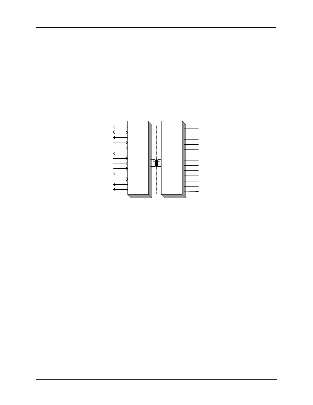
The 73M1922 MicroDAA chipset co nsists of a 73M1902 and a 73M1912. The 73M1902 is the Host
Interface Chip ( HIC) providi ng a host microprocessor or DS P in terface by a synchronous serial port
(Modem Analog Front En d ( M AFE ) ) and the 73M1912 is the Line Interfac e C hip ( LIC) t o connect to a
telephone line.
The 73M1922 chipset is packaged in two 20-pin TSSOP or two 32-pin QFN pack ages for a v ery small
ph ysical dimension and offers l ow cost global DA A design.
The 73M1922 performs a modem codec funct i on that interfac es a Host/ D SP and the PSTN (Pu blic
Switc hed Telephone Network). The codec suppor ts data rat es up t o V.92 with cal l progress signal i ng. In
add i tion to the c odec functi o n, t he 73M192 2 Mic r oD AA ch ipset also performs other necessary DAA
functions, such as CI D (caller i dentification) , rin g detection, tip/ring polar ity reversal detecti on, on/off hook
switch contr ol, p ulse di al ing , regu l ation of loop current (DC-I V), l ine impedance matching, line in use and
parall el p ickup det ection.
All data and control inform ation between the LIC and the HIC is transferred across a low cost pulse
transformer barrier. Also all clock and synchronization information needed in LIC is embedded in this
data and control bit stream acros s the b ar r ier transfor mer rec eived from H IC an d recons tructed within
LIC. The LIC interface to tip/ring of the PSTN significantly lowers the number of external components and
their cost.
The DAA feature integrated in this chipset offers a configurable US, ETSI ES 203 021-2, or other World
Wide DAA capability to t he tel ephone line interface an d an auxiliary DAC with gain con trol for line
monitoring during the call pr ogress period.
Rev. 5.1 5
Figure 1: MicroDAA System Block Diagram

73M1922 Demo Board User M anual UM_1922_006
1.1 Package Contents
The 73M1922 Demo Board Kit includes:
• A 73 M 1922 D em o Board ( R ev. D1)
• The follo wing documents on CD:
• 73M1922 Demo Board User Manual (this document)
• 73M1822/73M1922 Data Sheet
• 73M1822/73M1922 Layout Guideline
• 73M 1x2 2 Wor ldwide Design Guide
1.2 Safety an d ES D Notes
Connecting live voltag es to the Demo Board syst em will result in potential l y hazard ous volt ages on the
boards.
Extreme caution should be taken when handling the Demo Boards after connection to
live voltages!
The Demo Boards are ESD sensitive! ESD precautions should be taken when handling
these boards!
1.3 Demo Board Options
The 73M1922 Demo Board has 20-pin right angle connect or s to plug on to a target DSP or CPU system.
Each has a 3 .3 V power recep tacle for powering on-b oar d cir cuits from target system or ext er nal p ower
supply, or power can be supplied through the 20-pin connector along with the other signals. The
73M1922 Demo Boar d allows the evaluat ion of the 73M1922 chipset for un iversal mod em , voice
app l icati on and inter fac e to a general DSP or C PU system use.
6 Rev. 5.1

UM_1922_006 73M1922 Demo Board User Manual
2 Connectors
Table 1 shows all the connectors and jumper s available on 73M192 2 M i croDAA Demo Board. JS1 is the
main connector for i nterfacing to a host proces sor or DSP b oar d. Li ne mon i tor/C al l progress mon it or
speaker and dri ver c ircu i ts are also on board. J1 is a mod ular connector for phone li ne connec tion and J4
is for power connection from the main board or an external power supply.
Table 1: 73M1922 Demo Board Connectors
Sche matic and PCB
Reference
JS1 3M CONN.
Name Description
20-pin connect or to interface 73M1922 Demo Boar d to a
10X2
HOS T controller m ai n boar d.
J1 RJ-11 Telephone l ine connector.
J2 3.3 V suppl y Plug for connectin g external 3.3 V DC power supply.
Table 2: 73M1922 Demo Board Configuration Settings
Sche matic and PCB
Reference
Name Description
R54 (20 TSSOP DB), TYPE Fram e Sync Type:
0 Ω population: Late FSB (Default for Samsung ARM9
Interface).
None: Early FSB.
R64 (32 QFN DB only) MODE SCLK mode:
0 Ω population: 32 Clock.
None: Continuous SCLK. (Default for Samsung ARM9
Interface)
* NOTE: Due to the packag e r estrictions, the MODE pin i s not available in a 20-pin TSSOP package.
And neither the Mode pin nor the TYP E pi n is avail able in 42-pin QFN package. User should choose the
right device opti on when or dering parts depending on th e clock m ode (32 clock or continuous ) and Frame
sync type (early or l ate frame sync) required. Refer to the ordering information section of the
73M1822/73M1922 Data Sheet.
Table 3: JS1 Host Interface Connector
PIN Number Name Description PIN Number Name Description
1
2
NC
VCC 3.3V power
11
12
RINGD Ring Det.out
NC
supply
3
4
5
6
7
8
9
10
NC
RESET Reset Input
NC
NC
NC
NC
RINGD Ring Det.out
NC
13
14
15
16
17
18
19
20
NC
NC
AFEIN Serial Data In
AFEOUT Serial Data Out
SCLK Serial Clock
FS Frame Sync
NC
GND Ground
Rev. 5.1 7

R4
100K, 1%
R2
10M
C7
1uF
R6
100K, 1%
C12
0.1uF
U2
73M1912
OFH
4
VND/VNX
5
SCP
6
MID
7
VPX
8
SRE
9
SRB
10
VBG
11
ACS
12
VNS
13
VPS
14
RXP
15
RXM
16
TXM
17
DCD
18
DCE
19
DCB
20
DCI
1
RGN
2
RGP
3
L1 2kOhm
R5
8.2
-+
BR1
HD04
4
1
3
2
C43
1nF
Q4
MMBTA92
1
3 2
C26 1nF
C48
0.01uF
J1
RJ-11
1
2
3
4
5
6
C38
0.1uF
C24
NC (1nF, 3kV)
C41
220pF
R12 5.1K
TP15
VPS
1
C37
0.01uF
C35
220pF, 3KV
C9
0.47uF
L2 2kOhm
C13
15pF
F1
TRF600-150
R8
100K, 1%
Q7
MMBTA42
1
32
TP14
OFH
1
R58 1K
C50
100pF
R3 412K, 1%
Q3
MMBTA42
1
3
2
R65 200
C47
1nF
C34
3,3uF
C28
1nF
C30
1nF
C31
1nF
VCC
VCC
C46
1nF
TP1
GND
1
C1
0.022uF, 250V
C3
0.022uF, 250V
NOTE: GND f or C 35 and C 36 c onnec t
to GND on t he H OST side of t he barrier
TB3100H
GND
C14
15pF
T1
Pulse TFR
1 4
2 3
D1
MMSZ4710
1
2
VCCVCCVCC
C29
3,3uF
VCCVCC
C22
3,3uF
R67 1M, 1%
R53
49.9
R52 49.9
R11
3K
GND
R66 1M, 1%
C21
3.3uF
GND
VCC
TP16
FSBD
1
R51
49.9
U1
73M1902
FSBD
1
AOUT
8
VPT/VPD
15
TYPE
9
OSCIN
5
OSCOUT
6
VPA/VPM
10
VNM/VNT
11
SCLK
17
SDOUT
20
SDIN
19
VND
3
FS
2
VPD
4
VNPLL
7
M/S
12
PRM
13
PRP
14
INT
16
VND
18
VCCVCC
U3
NJM#2135M
CD
1
-VIN
4
V+
6
GND
7
VOUT1
5
VOUT2
8
VREF1
2
VREF2
3
R50
49.9
8DMP
R48 20K
LS2
Projects U nlim it ed
AST-2308MR-R
C27
1uF
R46 120K
R49
20K
C25
3,3uF
C45 0.1uF
VCCVCCVCC
VCCVCCVCC
C19
27pF
C17
0.1uF
C18
27pF
C33
0.1uF
C15
0.1uF
J4
3.3V POWER
3
3
1
1
2
2
R54 0
JS1
CONN SOC KET 10X2
2
4
6
8
10
12
14
16
18
20
1
3
5
7
9
11
13
15
17
19
R61 1K
C32
3.3uF
R9 100K, 1%
C10 0.47uF
R10
255, 1%
C8
4.7uF
C4
2.2uF
VCC
Q5
MMBTA06
1
32
TP10
TXM
1
C36
220pF, 3KV
Y2
24.576MHz
13
24
Q6
BCP56
1
2
3
4
TP18
VNS
1
C49
0.1uF
E1
P3100SBRP
C6
1uF
73M1922 Demo Board User Manual UM_1x22_006
3 Demo Board Schematics, PCB Layouts and Bill of Materials
3.1 Schematic
8 Rev. 5.0
Figure 2: 73M1922 MicroDAA 20-Pin TSSOP Demo Board Schematic Diagram

UM_1922_006 73M1922 Demo Board User Manual
3.2 73M1922 20-Pin TS SOP Demo Board Lay out
Figure 3: 73M1922 20-Pin TSSOP Demo Board: Top Signal Layer
Figure 4: 73M1922 20-Pin TSSOP Demo Board: Layer 2, Ground Plane
9 Rev. 5.0

73M1922 Demo Board User Manual UM_1922_006
Figure 5: 73M1922 20-Pin TSSOP Demo Board: Layer 3, Supply Plane
Figure 6: 73M1922 20-Pin TSSOP Demo Board: Bottom Signal Layer
10 Rev. 5.0

UM_1922_006 73M1922 Demo Board User Manual
Figure 7: 73M1922 20-Pin TSSOP Demo Board: Silk Screen Top
Figure 8: 73M1922 20-Pin TSSOP Demo Board: Silk Screen Bottom
Rev. 5.0 11

73M1922 Demo Board User Manual UM_1922_006
3.3 Demo Board P hy sica l Dimensions
PCB Dimensions
• Size
73M1922DB 3.16 x 2.05” (80.20 x 52.50 mm)
Height w/ components and solder
73M1922DB 0.65” (16.5 mm)
Environmental
• Operating Temperature °-40 to +85°C
(function of crystal oscillator affected outside –10°C to +60°C)
• Storage Temperature -65 to 150°C
Power Supply
• DC Input Voltage (powered from DC supply) 3.3 VDC ±10%
• Supply Current 25 mA (off-hooked at room temperature) typical
12 Rev. 5.0

UM_1922_006 73M1922 Demo Board User Manual
Qty
Reference
Part
DigikeyPN
MFRPN
MFR
1
BR1
HD04
HD04DICT-ND
HD04-T
DIOD E S In c.
2
C1,C3
0.022uF, 250V
399-1242-1-ND
C1206C223K5RACTU
Kemet
1
C4
10uF
399-3522-1-ND
C0805C225K8RACTU
Kemet
2
C6,C7
1uF
587-1241-1-ND
EMK107BJ105KA-TR
Taiyo Yuden
1
C8
4.7uF
PCC2176CT-ND
ECJ-2FB0J475M
Panasonic
2
C10,C9
0.47uF
PCC1911CT-ND
ECJ-1VB0J474K
Panasonic
6
C12,15,17,33,38,49
0.1uF
399-1095-1-ND
C0603C104K8RACTU
Kemet
2
C14,C13
15pF
445-1271-1-ND
C1608COG1H150J
TDK
2
C19,C18
27pF
PCC270ACVCT-ND
ECJ-1VC1H270J
Panasonic
4
C21,C22,C32,C34
3.3uF
PCC1925CT-ND
ECJ-2YB0J335K
Panasonic
2
C35,C36
220pF, 3KV
445-2380-1-ND
C4532COG3F221K
TDK
8
C26,28,30,31,39,43,46,47
1nF
PCC1772CT-ND
ECJ-1VB1H102K
Panasonic
2
C37,C48
0.01uF
478-1227-1-ND
06035C103KAT2A
AVX
1
C50
100pF
311-1069-1-ND
CC0603JRNP09BN101
Yageo
1
C51
220pF, 630V
445-2338-1-ND
C3216COG2J221J
TDK
1
E1
TB3100H
TB3100H-FDICT
TB3100H-13-H
DIODES
1
F1
TRF600-150
576-04611.25ER
04611.25ER
Littlefuse
1
JS1
CONN 10X2
517-8520-4500
8520-4500JL
3M 1 J1
RJ-11
A31420-ND
5555163-1
AMP/Tyco
1
J4
POWER CONN
SC237-ND
RAPC712X
Switchcraft Inc.
2
L1,L2
100MHz, 200mA
240-2396-1-ND
HZ0805C202R-10
Steward
2
Q3,Q7
MMBTA42
863-MMBTA42LT1G
MMBTA42LT1G
ON Semi.
1
Q4
MMBTA92
863-MMBTA92LT1G
MMBTA92LT1G
ON Semi.
1
Q5
MMBTA06
863-MMBTA06LT1G
MMBTA06LT1G
ON Semi.
1
Q6
BCP56
568-1639-1-ND
BCP56
Philips
1
R2
10M
541-10.0MCCT-ND
CRCW080510M0FKEA
Vishay
1
R3
412K, 1%
P412KHTR-ND
ERJ-3EKF4123V
Panasonic
4
R4,R6,R8,R9
100K, 1%
P100KHCT-ND
ERJ-3EKF1003V
Panasonic
1
R5
8.2
541-8.20CCT-ND
CRCW08058R20FNEA
Vishay
1
R10
255, 1%
311-255HRCT-ND
RC0603FR-07255RL
Yageo
1
R11
3K
311-3.00KHRCT-ND
RC0603FR-073K0L
Yageo
1
R12
5.1K
311-5.10KHRCT-ND
RC0603FR-075K1L
Yageo
4
R50,R51,R52,R53
49.9
P49.9HCT-ND
ERJ-3EKF49R9V
Panasonic
1
R54 0 P0.0GCT-ND
ERJ-3GEY0R00V
Panasonic
2
R58,R61
1K
P1.00KHCT-ND
ERJ-3EKF1001V
Panasonic
1
R65
200
P200HCT-ND
ERJ-3EKF2000V
Panasonic
2
R67,R66
1M, 1%
311-1.00MCRCT-ND
RC0805FR-071ML
Yageo
2
TP1,10, 14, 15,16,18
Test Points
5002K-ND
5002
Keystone
1
T1
Pulse TFR
ESMIT-4180/750110001
Sumida//Midcom
1
U1
73M1902
73M1902
Teridian
1
U2
73M1912
73M1912
Teridian
1
Y2
24.576MHz
815-ABMM2-24.576-E2T
ABRACON
3.4 Bill of Materials
Table 4: 73M1922 20-Pin TSSOP Dem o Board Bill of Materials
2kOhm@
Rev. 5.0 13
ABMM2-24.576MHZ-E2-T

73M1922 Demo Board User Manual UM_1922_006
3.5 Pin Descriptions
Table 5 shows the 73M1902 20-pin TSSOP package pin names and Table 6 s hows the 73M1912 20-pin
TSSO P package pin definitions.
Table 5: 73M1902 HIC 20-Pin TSSOP Package Pin Definitions
Pin Name Pin Name
1 FSD 11 VNM/VNT
2 FS 12 M/S
3 VND 13 PRM
4 VPD/VPPLL 14 PRP
5 OSCIN 15 VPT/VPD
6 OSOUT 16 INT/RGDT
7 VNPLL/VNA 17 SCLK
8 AOUT 18 VND
9 TYPE 19 SDIN
10 VPA/VPM 20 SDOUT
Table 6: 73M1912 LIC 20-Pin TSSOP Package Pin Definitions
Pin Name Pin Name
1 DCI 11 VBG
2 RGN 12 ACS
3 RGP 13 VNS
4 OFH 14 VPS
5 VNX/VNS 15 RXP
6 SCP 16 RXM
7 MID/LEV 17 TXM
8 VPX 18 DCD
9 SRE 19 DCE
10 SRB 20 DCB
14 Rev. 5.0

UM_1922_006 73M1922 Demo Board User Manual
73M1902
1
2
3
4
5
6
7
8
9
10 11
12
13
14
15
16
17
18
19
20
FSD
FS
VND
VPD/VPPLL
OSCIN
OSCOUT
VNPLL/VNA
AOUT
VPA/VPM VNM/VNT
SDIN
SCLK
INT
VND
VPT/VPD
M/S
PRM
PRP
SDOUT
TYPE
73M1912
1
2
3
4
5
6
7
8
9
10 11
12
13
14
15
16
17
18
19
20
DCI
RGN
RGP
OFH
VND/VNX
SCP
MID
VPX
SRE
SRB VBG
DCE
DCD
TXM
RXM
RXP
ACS
VNS
VPS/VPD
DCB
3.5.1 731922 Micr oDAA Pinout
Figure 9 shows the pinout top views of the 73M1902/73M1912 TSSOP packages.
Figure 9: 73M1902/73M1912 20-Pin TSSOP Packages: Pinout (top view)
4 Related Documentation
The following 73M1x22 documents ar e availab le from Teridian Semiconductor Corp or ation:
73M1822/73M1922 Dat a Sheet
73M1922 Demo Board User Manual (this document)
73M1822/73M1922 Layout Guideline
73M1x22 Worldw ide Design G uide
73M1822/73M1922 Evaluation System with Linux Softmodem User’s Guide
73M1x22/73M1x66B MicroDAA DC Control Loop Operation
73M1x22/ 73 M 1x 6 6 Mi cr oDAA Hy bri d O p er ation
5 Contact Information
For m or e i nform ation about Teridian Sem i conductor p r oduct s or to c heck the availability of the 73M1922,
contact us at:
644 0 Oak Canyon Road
Suite 100
Irvin e, CA 92618-5201
Telephone: (714) 508-8800
FAX: (714) 508-8878
Email: modem.support@teridian.com
For a complete list of worldwid e sales offices, go to http://www.teridian.com.
Rev. 5.0 15
 Loading...