


Simplifying System IntegrationTM
73M1822
Keychain Demo Board Us er Manual
March 9, 2010
Rev. 5.0
UM_1822_007

73 M1 822 Keych ai n Demo Board User M anual UM_1822_007
© 2010 Teridian Semi conductor Corporati on. Al l r ights r eserved.
Terid i an Semiconductor Corporation is a registered trademark of Terid ian Semiconductor Corporation.
Simplifying System Integration is a trademark of Terid i an Semiconductor Corporation.
MicroDAA is a register ed trad emark of Teridian Semiconduct or Corporati on.
Micros oft is a registered trad emark of Microsoft Corporation.
Windows is a regi stered tradem ar k of Microsoft Corporation.
All other trademark s are the propert y of t heir respective owners .
Terid i an Semiconductor Corporation makes no warranty for the use of its products, other t han expressly
contained in the Company’s warranty detailed in the Teridian S emiconductor C or poration stan dard Term s
and C onditions. The company assumes no responsibilit y fo r any errors which may appear in this
document, reserves the right to change devices or specifications det ai led herei n at any t ime with out
notice and does not make any commitment to updat e the information contained her ein. A ccordingly, the
reader is caut i oned to verify that th i s document is cur r ent by comparing it to the l atest versi on on
http://www.teridian.com or by checki ng with you r sales representative.
Terid i an Semiconductor Corp., 6440 Oak Canyon, Sui te 100, Irvine, CA 92618
TEL (714) 508-8800, FAX (714) 508-8877, http://www.teridian.com
2 Rev. 5.0

UM_1822_007 73M1822 Keychain D emo Board User Manual
Table of Contents
1
Introduction ................................................................................................................................... 5
1.1 Pack age Contents.................................................................................................................... 6
1.2 Safety and E SD Notes ............................................................................................................. 6
1.3 Demo Board Options................................................................................................................ 6
2 Connectors .................................................................................................................................... 7
3 Software Description ..................................................................................................................... 8
3.1 System Initialization ................................................................................................................. 8
3.2 73M1822 Sys te m Ini ti aliz a ti o n .................................................................................................. 9
3.3 Off-H ook Procedure ............................................................................................................... 11
3.4 Dialing ................................................................................................................................... 12
3.4.1 DTMF Dialing .............................................................................................................. 12
3.4.2 Pulse Dialing ............................................................................................................... 12
3.4.3 Adapt ive Dialing .......................................................................................................... 14
3.5 LINE Sensing ......................................................................................................................... 15
3.5.1 Line-In-Use (LI U) - Prior to the Modem Goi ng Off-Hook............................................... 16
LIU Check Procedure ............................................................................................................. 17
3.5.2 Parallel Pick Up (PPU) - While the Modem is Off-Hook................................................ 17
3.5.3 PPU Check Pr ocedure ................................................................................................ 18
3.6 Ring Detect ............................................................................................................................ 18
3.6.1 Ring Detection Setup with Hardware Ring Qualifier ..................................................... 19
3.6.2 Ring Detection Using Coarse Ring Output ................................................................... 20
3.7 Line Polarity Reversal Detection............................................................................................. 20
3.8 Line Snoop / Type I Caller ID Detection .................................................................................. 21
4 Demo Board Schematics, PCB Layouts and Bill of Materials ................................................... 24
4.1 Schematic .............................................................................................................................. 24
4.2 73 M1 822 Mic r oDAA Demo Board PCB Layout ....................................................................... 25
4.2.1 73M1822 42-Pin QFN Keychain Demo Board L ayout .................................................. 25
4.2.2 Keych ain Dem o Board Physical Di mensions ............................................................... 27
4.3 Bill of Materials ...................................................................................................................... 28
4.4 Pin Descriptions ..................................................................................................................... 28
4.4.1 731822 Pinout............................................................................................................. 30
5 Related Documentation ............................................................................................................... 31
6 Contact Information ..................................................................................................................... 31
Rev. 5.0 3

73 M1 822 Keych ai n Demo Board User M anual UM_1822_007
Figures
Figure 1: Mic r oDAA System Block Diagr am
Figure 2: 73 M 1822 Register Polling
Figure 3: Off-Hook Procedure
Figure 4: Pulse Dialing Sequence
Figure 5: Dialing
Figure 6: Adapt ive Dialing
Figure 7: Line-In-Use Det ection
Figure 8: On-Hook TIP-RING DC Reading
Figure 9: Par allel Ph one Off-Hook Detection
Figure 10: Ring Qualifier
Figure 11: R ing Detec tor
Figure 12: Line Polarity Reversal Detection
Figure 13: C aller ID Detection Path
Figure 14: 73M1822 K eyc hain Demo Board Schematic
Figure 15: 73M1822 K eyc hain Demo Board : Top Signal Layer and Silk Screen
Figure 16: 73M1822 K eyc hain Demo Board : Layer 2, Ground Plane
Figure 17: 73M1822 Keychain Demo Board: Layer 3, Supply Plane
Figure 18: 73M1822 K eyc hain Demo Board : Bottom Signal Layer and Silk Screen
Figur e 19: 73M1822 QFN 42-Pin Package: Pinout (top view)
............................................................................................. 5
......................................................................................................... 8
................................................................................................................ 12
.......................................................................................................... 13
.................................................................................................................................... 14
...................................................................................................................... 15
............................................................................................................. 16
............................................................................................. 17
.......................................................................................... 18
........................................................................................................................ 19
........................................................................................................................ 20
............................................................................................ 20
........................................................................................................ 21
.......................................................................... 24
..................................... 25
...................................................... 25
....................................................... 26
................................ 26
................................................................. 30
Tables
Table 1: Host Interface JP2 Connector Pinout
Table 2: Lin e Interface JP1Connector Pinout
Table 3: 73M 1822 Keych ai n Demo Board Bi ll of Materia ls
Table 4: 73M1822 42-Pin QFN Package Pin Definitions
.......................................................................................... 7
........................................................................................... 7
..................................................................... 28
......................................................................... 29
4 Rev. 5.0
GPIO
FS
FSD
SCLK
SDIN
SDOUT
M/S
INT/RGDT
OSCIN
OSCOUT
H
O
S
T
I
N
T
E
R
F
A
C
E
L
I
N
E
I
N
T
E
R
F
A
C
E
RGP
RGN
OFH
DCI
DCB
DCE
TXN
RXM
RXP
SRE
ACS
SRB
DCD
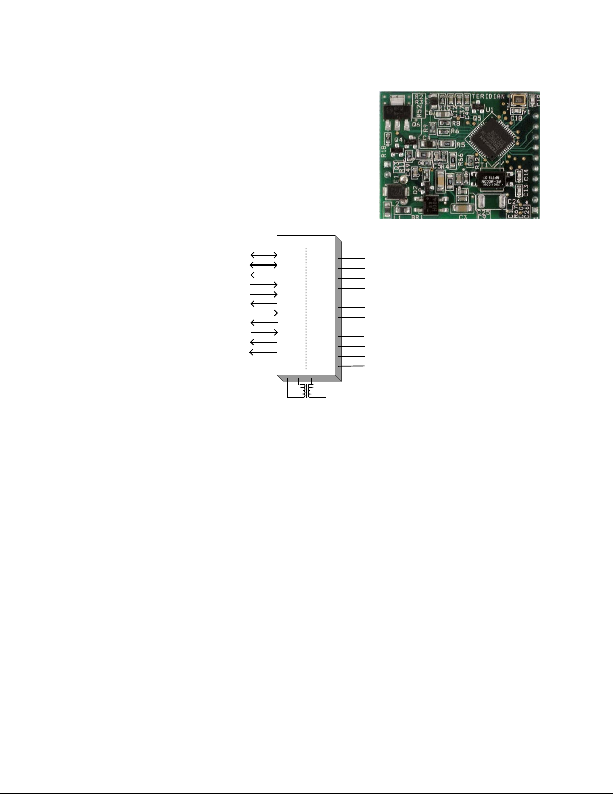
73M1822
PULSE
TRANSFORMER
73M1822
Line Interface
Circuitry
Host Interface
Circuitry
AOUT
UM_1822_007 73M1822 Keychain D emo Board User Manual
1 Introduction
The 73M1822 Keychain Demo Board integrates silicon Data
Acc ess Arrangemen t (DAA) fun ction al ong with Analog Front End
functions chipsets for worldwide com pliance.
The 73M1822 MicroDAA is the world’s first single chip silicon DAA
IC t hat perform the ad vanced si licon Data Access Arrangement
(DAA) function along with Analog Front End functions.
The 73M 1822 MicroDAA i s available in a 42 pi n QFN pac kage for a
very small physical dimension and offers low cost global DAA
design.
Figure 1: MicroDAA System Block Diagram
The 73M1822 performs a modem codec function that interfaces a Host/DSP and the PSTN (Publ ic
Switc hed Telephone Network). The codec supports data rates up to V.92 with call progress si gnaling. In
add i tion t o the codec f unc t ion, the 73M1822 MicroDAA also performs other necessary DAA functions,
such as CID (caller identification), r i ng d etection, tip/ring polari ty reversal detection , on/off hook swit ch
control, p ulse dialing, r egulation of loop current ( D C-IV), line impedanc e m atching, line in use and parallel
pickup detection.
All dat a and control information between t he LIC an d the HIC is trans ferr ed across a low cost pulse
tran sformer b ar r ier. Also all cl ock and synchr onizati on information needed in LIC is embedded in this
data and control bit stream across the barrier transfor mer received from HIC and reconstructed within
LIC. The LIC interface to tip/ring of the PSTN significantly lowers the number of external components and
their cost.
The DAA feature integr ated in this device offers a config urable U S, TBR21, or other World Wide DAA
capability t o the telephon e l ine interface and an auxili ary DAC with gain contr ol for lin e monitoring during
the call progress p er i od.
Rev. 5.0 5

73 M1 822 Keych ai n Demo Board User M anual UM_1822_007
1.1 Package Contents
The 73M1822 Keychain Demo Boar d Kit in cludes:
• A 73 M 1822 Keychain Demo Board ( R ev. D1)
• The following documents on CD:
• 73M1822 Keychain Demo Board User Manual (this document)
• 73M1822/73M1922 Data Sheet
• 73M1822/73M1922 Schematic and Layout Guidelines
• 73M 1x2 2 Wor ldwide Design Gui de
1.2 Safety an d ES D Notes
Connecting live voltages to the Demo Board system will result in potentially h azardous voltages on the
boards.
Extreme caution should be taken when handling the Demo Boards after connection to
live voltages!
The Demo Boards are ESD sensitive! ESD precautions should be taken when handling
these boards!
1.3 Demo Board Options
The 73M1822 Keychain Demo Board has 20-pin right angle connect or s to plug on to a target DSP or
CPU system. Each has a 3. 3 V power receptacle for power i ng on -board cir cuits from target system or
external power supply, or power can be supplie d t hr o u gh the 20-pin connector along with the oth er
signals. The 73M1822 Keychain D emo Board allows the evaluat ion of t he 73M1822 device for universal
modem, voice ap plicat i on and i nterface to a general D SP or CPU system use.
6 Rev. 5.0
UM_1822_007 73M1822 Keychain D emo Board User Manual
2 Connectors
Table 1 and Table 2 show all the connectors and jumpers available on 73M1822 Keychain Demo B oar d.
JP2 is the mai n connec tor for int er facing to a host processor or DSP board. JP1 is a connector for ph one
line connec tion. Be aware that there is no high voltage and current protection circuit included in any
Keych ain Dem o Boards. Make sur e these protection circuit components ar e placed i n between t he
telephone li ne and JP1 connector for a practical design. Line monitor/Call pr ogress monit or speaker and
driver circuits are not available on the Keychai n Demo Boards. Refer to the 73M1822 Keychain Demo
Board schematics for t he protection circui t and Call Progress Monit or circui t referen ces.
Table 1: Host Interface JP2 Connector Pinout
PIN Number Name Description
1
2
3
4
5
6
7
8
9
10
FSBD Delayed FS
RINGD Interrupt Output
VCC 3.3V Su ppl y
RESET Reset Input
AOUT Call progress Monitor ou t
GND Power Signal GND
FS Fram e Sync
SCLK S erial Clock
AFEIN Serial Data In
AFEOUT Serial Data Ou t
Table 2: Line Interface JP1Connector Pinout
PIN Number Name Description
1
2
TIP Phone Line Connection
RING Phone Line Connection
Rev. 5.0 7
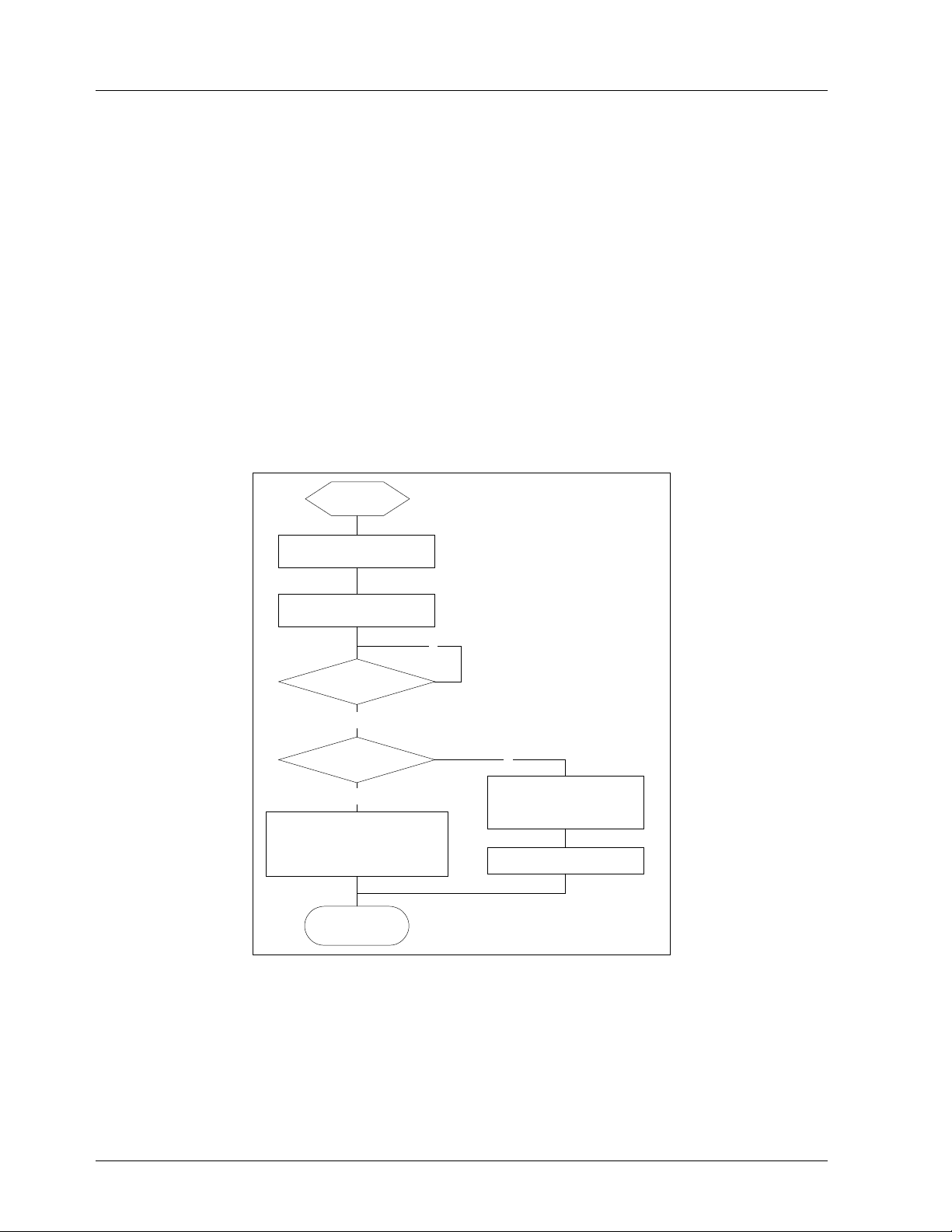
LIC ADD -> INDX3:0
(Reg19:3-0)
1-> POLL (Reg 19:7)
POLL(Reg19:7)=0?
MATCH(Reg19:6)=1?
Both HIC and LIC registers
specified by the ADD are
synchronized
Read POLLVAL(Register1F)
END
y
y
n
START
The HIC and LIC registers
specified by the ADD are
different
n
Error Handling
73 M1 822 Keych ai n Demo Board User M anual UM_1822_007
3 Software Description
3.1 System Initialization
This s ection describes softwar e that is not provided with the 73M1822 Keychain Demo Board but must be
provid ed by the Host sys tem.
Once the system starts initialization, the system controll er al so needs to initialize the 73M1822 device set
as one of its peripheral. Some register s contain both control and status bits which are read only. When
using READ-MODIFY-W RITE to update an HIC regis ter, care must be taken not to modify the status and
control bits unintentionally.
Upon power on reset, the HIC registers that contains the copy of the LIC reg isters (Register 0x12
to Register 0x1F) will be initialized to the default reset value. When the power of LIC is fed from
the HIC by setting the ENFEF bit (Register 0x0F Bit 7), LIC will be initialized with the default
register value that are identical to the values in register copy in LIC. Form this point, Any host
control to the LIC register bits by wri ting to an HIC register which is copy of the LIC register will
change both HIC and LIC maintaining images of each other unless data errors occur. In this
situation, there is a LIC register polling mechanism to regain this synchronization by host control.
Figure 2 illustrates how to re-synchronize the HIC and LIC registers by polling.
8 Rev. 5.0
Figure 2: 73M1822 Register Polling

UM_1822_007 73M1822 Keychain Demo Board User Manual
3.2 73M1822 System Initialization
The following exampl e shows the sequ ence to bri ng the 73M18 2 2 MicroDAA out of reset and to s tart up
after power up.
NOTE: The 73M1822 MicroDAA does n ot have a power on reset c ircuit. For p r oper operation, a reset
signal shall be asserted from the host by pulling the reset pin of 73M1822 low ap proximately for 100 ns or
longer after the power is stabil i zed. The 73M1822 device will be ready to use within 100 μs after the
remov al of reset pulse from th e r eset pin.
Resetting the 73M1822
The 73M1822 package does not have a dedicated res et pin due to pin restriction. An alternative reset
can be assert ed through the M/S pin (pi n 21 of 73M1 822 42-pin QFN).
Any low-to-high or high-to-low transition at this pin will r esult i n int er nal reset block to initiat e the reset
process. So if the MA FE needs to be in MASTER configuration, the h ost needs to generate an active low
reset signal as a reset si gnal at this pi n. Use act ive high res et signal for SLAVE mode of MAFE
applications.
• Power up the system.
• Wait for 3.3V power to be stable
• Pull M/S pin low for 100 ns then let it go high if the 73M1822 is in Master configuration. (Pull M/S pin
high for 100 ns or longer then l et it go low in case of slave configuration)
• Wait for 100 μs for PLL, OS C to be stabilized
Initializing MicroDAA
A. Frame Synchronization
• RESET HC bit (Register 0x01 bit 0) in a frame sequence.
• RESET HC bit (Register 0x01 bit 0) in next frame sequence.
• Then the HIC is guaranteed t o be i n software controlled con trol frame mod e, now. All the MAFE
serial data sh all be data only unless host req uest by setting bit 0 of data.
B. Control Frame Generation
Software Controlled Control Frame
• MAS K C TL (TXD Bit 0) as 1 to request a subsequ ent cont r ol frame.
• Write or read t he 73M18 22 HIC regi ster using the MAFE control data form at.
• Make sure to MASK CTL (TXD bit 0) as 0 if the control frame is not needed.
Hardware Controlled Control Frame
• MAS K TX D Bit 0 as 1 to request a subsequent c ontrol frame.
• SET HC bit (Register 0x01 bit0) using the MAFE control dat a format in the next frame.
• From now on, there will be data and control frames alternating. Make sure not to miss this sequence.
Rev. 5.0 9

73 M1 822 Keych ai n Demo Board User M anual UM_1822_007
C. 73M1822 HIC Initialize
• Disable daisy chain by writin g 00H to HIC Register 0x01.
• Configure eit her Hardware con trol frame or software control frame by sel ecting the HC bit (Register
0x02:0).
• Configure GPIOs by s el ecting GPIO Data (Regis ter 0x03), GPIO Direction (Register 0x04), GPIO
Interrupt Enable (Register 0x05) and Interrupt Polarity (Register 0x06).
• Timing Chain setup ( R egister 0x08 - - Regi ster 0x0 D). Register 0x0D value shall be written the last.
An y ot her writes to Register 0x08 to Regi ster 0x0C are not r eal ly affec ting to the PLL until Register
0x0D is being written . It is also recommended to set CHNG FS (Register 0x0D:3) bit in case further
sample rate c hanges are r equired for such as V.90 appli cations.
• En able Analog Front End blocks by setting ENFEH bit (Register 0x0F:7). And put device active by
clearing SLEEP bit (Register 0x0F:5).
• Select system clock driven from PLL by setting FRCVCO bi t of Register 0x0E bit 7. (The FR C VCO
bit shall be s et at least 2 sample period aft er writi ng t o R egister 0x0D.)
D. LIC Init
73M1822 LIC initialization shall beg in aft er the73M1822 LIC part is fully powered up and initialized. From
the HIC Initialization above, setting ENFE then the FRVCO bits will start powering the 73M1822 LIC.
From this moment, the Host shall wait for 10 0 to 200m s for t he 73 M1 822 LIC t o be ready.
• Enable Front End functional blocks by setting ENFE bit (Register 0x12:2)
• Write 0x01 t o Regist er 0x18.
• Select prop er fi l ter setting per each sample rat e setting FSCTR b its (Register 0x16:3-0)
• Select prop er AC impedance termination by setting AC Z31,0 (Register 0x17: 4, 3)
• Enable receiver path by setti ng RXEN bit ( Regis ter 0x16:6)
Example 1. Using Software Controlled Control Frame:
static const U16 init_afe_config[] = // Must have Data(LSB=1) , Control,
// Data(LSB=1), Control,.. FRAMES
{
REG02|0x00, REG02|0x00, // Forc e to Software controlled c ontrol frame (HC=0)
CTRL_FRAME, REG04|0x00, // GPIO 7,6,5,4 = outputs
CTRL_FRAME, REG03|0x00, // GPIO 7,6,5,4 output data =0000
CTRL_FRAME, REG05|0x00,
CTRL_FRAME, REG06|0x00,
CTRL_FRAME, REG07|0x00,
CTRL_FRAME, REG08|AFE_CTRL08, // Timi ng chain set up (Smaple Rate)
CTRL_FRAME, REG09|AFE_CTRL09,
CTRL_FRAME, REG0A|AFE_CTRL0A,
CTRL_FRAME, REG0B|AFE_CTRL0B,
CTRL_FRAME, REG0C|AFE_CTRL0C,
CTRL_FRAME, REG0D|AFE_CTRL0D,
CTRL_FRAME, RW B|REG03, // Del ay for 2 sample cycl e time t o
CTRL_FRAME, RW B|REG03, / / let PLL settle before Lockdet by dummy read
GPIO
CTRL_FRAME, REG0F|0x8C / / Set ENF E Bit, Reset Sleep Bit
CTRL_FRAME, REG0E|0x80 // Set FrVCO bit
};
note: CTRL_FRAME = 0x0001
10 Rev. 5.0

UM_1822_007 73M1822 Keychain Demo Board User Manual
Example 2. Using Automatic Control Frame (Hardware Controlled Control Frame):
static const U16 init_afe_config[] = // MUST HAVE Dummy Data, Control, .. FRAMES
{
REG02|0x00, REG02|0x00, // F or ce to Software cont r olled control frame
CTRL_FRAME, REG02|HC, // Enable Hardware contr ol led con trol frame
0x0000, REG04|0x00, // GPIO Direction
0x0000, REG03|0x00, // GPIO Data
0x0000, REG05|0x00, // GPIO interrupt control
0x0000, REG06|0x00, // GPIO
0x0000, REG07|0x00,
0x0000, REG08|AFE_CTRL08, // Timing chain set up
0x0000, REG09|AFE_CTRL09,
0x0000, REG0A|AFE_CTRL0A,
0x0000, REG0B|AFE_CTRL0B,
0x0000, REG0C|AFE_CTRL0C,
0x0000, REG0D|AFE_CTRL0D,
0x0000, RWB|REG03, // Dum my Data, D elay for 2 sampl e cycle time to
0x0000, RWB|REG03, // let PLL set tle before Lockdet by dummy read GPI O
0x0000, REG0F|0x8C // Set ENFE Bit, Reset S l eep Bit
0x0000, REG0E|0x80 // Set FrVCO bit
};
3.3 Off-Hoo k Proce dure
Off-ho ok control in MicroDAA is d ifferent fr om th at of a t r aditional DAA GPIO control m echanism. Due to
the commun i cation del ay between host and MAFE through the barrier interface, and poss ible error ov er
the channels, the O ff-hook control of silicon DAA is quite complic at ed. The host controller need s to go
thr ough many steps starting from initiating a Off-hook command by setting the OFH bit and waiting for the
status responses from the LIC and based on this s tatus deter mine the next step to proc eed.
The hos t cont r oller has to manage all of the Normal On/Off hook sequ ence as shown in the following flow
chart in Figure 3.
Off-Hook Procedure
• The MicroDAA system is in Barri er Power Mode. ( E NLPW bit (Register 0x02:2) =0)
• Go off-h ook by setting OFH (Reg ister 0x12:7) to turn the DC path to the DCgm and Acgm and Shunt
regulator bl ocks.
• En able DCgm that provid es appropriate DC curren t/voltage contr ol to the l i ne by setting E NDC
(Register 0x12: 6) bit.
• En able ACgm to provide a AC i mpedance mat ching to the line by setting ENAC (Register 0x12: 5) bi t.
• Enable Shunt loading ENSHL (Register 0x12:4) by writing 0xF6 to Register 0x12.
• Wait for 3 ms.
• Chec k if the volt age is too l ow by mon itoring UVDET (Register 0x1E: 6) is set by interrupt or polling.
• If there is no abnormality (UV DET=1) d etected, then go to nominal mode b y setting ENNOM bit
(Register 0x12:0) (Transition to NOMINAL Mode) Done/Ready
• If the UVDET bit (Register 0x1E: 6) was set, then power down the Shunt Regulator by resetting
ENSHL (Register 0x12: 4).
• Wait for 3 ms.
• Check if UVDET (Register 0x1E: 6) is set by interrupt or polling.
• If no abnormality detected, then go to nomin al mode by setting En NOM bit (Register 0x12:0)
(Tran sition to NOMINAL Mode) Done/Ready.
• If there is an abnorm al ity still , then determ ine the cause such as phone line is unplugged.
Rev. 5.0 11

Yes
No
AC,DC, Shunt Loading = Off
DLL, FSM, LSBI, BG = On
Disable UVDT INT (EnDT= 0)
Disable EnNOM(=0)
On Hook State
Mixed Mode
Go Off-hook
OFH=1,EnDC=1
EnAC=1,EnShl=1
Wait 3ms
Yes
No
EnNOM =1;
Enter Nominal mode;
Enable DT INT (EnDT=1)
Ready
Disable DT INT (EnDT=0)
Disable DT INT (EnDT=0)
Continue to Seize the Line
Wait 3ms
Enable DT INT(EnDT=1)
Yes
No
EnShl=0
Shunt Loading
EnShl=0
Go Off-hook?
INT?
INT?
*CP
NOTE: *CP for Call progres and dialing
73 M1 822 Keych ai n Demo Board User M anual UM_1822_007
Figure 3: Off-Hook Procedure
3.4 Dialing
3.4.1 DT MF Dialing
DTMF is c onsider ed to be a part of the mod em signal. The DTMF signals can be generated by th e host
DSP in a way simi lar to the other modem sig nals and transmi tted to the line through a ser ies of TBS data
frames sent from HIC t o LIC. After the syst em going to off-hook, call progress monitoring and dialing can
be execu ted as s hown in Figure 5.
3.4.2 Pulse Dia ling
Pu l se dialing can be performed by a host control . Figure 4 and Figure 5 show the control pr ocedure of
pu l se dialing with MicroDAA . A tone dial ing can follow a normal off-h ook procedure. An altern ative offhook sequence is shown in Figure 6 with pulse dialing mode enabled. After dialing the last pulse digit,
and j ust before going to an on-line (data) mode, setting the ENLPW bit (Register 0x12: 2) would bring the
line p ower to the 73M1822 LIC. The ENNOM (Register 0x12:0) bit setting will end the Pulse dialing to get
into the normal data m ode. There is delay from an OFH software bit control to actual out of the OFH
hardware pin due to th e barrier interfac e.
12 Rev. 5.0

LLM
EnNOM
Low BW
High BW
OFH
(REG12:B7)
On-hook
EnLPW
Normal 2 Wire Mode
PLDm (from Host)
Pulse Diagling Mode
Tone Dialing
Off-hook
OFH
(pin 2)
2ms
Off-hook
UM_1822_007 73M1822 Keychain Demo Board User Manual
Figure 4: Pulse Dialing Sequence
Rev. 5.0 13

73 M1 822 Keych ai n Demo Board User M anual UM_1822_007
*CP
Off-hook State
Dial tone detected
Inter-digit
Delay
Pulse Dialing?
PLDm=1
OFH=0
Wait for break time period
OFH=1
Wait for make time period
No
Yes
Is Pulse digit done?
More digit to dial?
No
Yes
Yes
No
PLDm=0
DTMF Tone on
Wait for On ti me
DTMF Tone off
Wait for Off time
more digit to dial
Yes
No
Done
Figure 5: Dialing
3.4.3 Adaptive Dialing
Adaptive dialing is a combination of DTMF and Pulse dialing. The MicroDAA system goes into an offhook condition without setting the EnNOM bit. First the dial tone detection is used to see if the line
supports DTMF by starting with DTMF dialing. After dialing the first digit using DTMF, if the dial tone
dis appears, cont in ue on tone dialin g. If the d ial tone is still p r esent after sending a DTMF tone, the li ne
cannot supp or t tone dialing so the system will di al in pulse mode from th e fir st digi t again. The host sets
the EnNOM bit after th e dialin g and call progress process i ng are done, but before the modem c onnection.
14 Rev. 5.0

Yes
Yes
Off-hook State
Dial tone detected
No
Dial Tone exist?
Done
PLDm=0
DTMF dial
PLDm=1
PULSE dial
DTMF dial
UM_1822_007 73M1822 Keychain Demo Board User Manual
Figure 6: Adaptive Dialing
3.5 LINE Sensing
For m odems used in set-top boxes and fax applicati ons, th e modem lines are t ypicall y bridg ed onto the
same phone line that provides t elephone service to the household. In this type of install ation, the mod em
is required to determine whether som eone is using the shared phone line or not. Th er e ar e two types of
shared ph one l ine acti vity detection. While the target system (MicroDAA) i s on-hook and the line is being
used by another device such as telephone, the target system should not go off-hook and interrupt the
other device. Thi s featu r e is called lin e in use (LIU) detection. The other feature is called parallel pick-up
detection ( PPU). While the target system is using the phone line (off-hook) , if another d evice sharing the
same line goes off-hook, the target system should free up the line by going on-hook immediat el y and
releasing the line to the other device. In most cases the 73M1822-based product will have the lowest
priority. In cases where the pr oduct is an alarm , it may have t he highest p r i or ity and other devices should
give up the line. The MicroDAA is capab l e of supporting this feature without additional external
components.
The line-sensing task is shared by HIC and LIC. The LIC, continuously, monitor s the lin e with integrated
auxiliary A/D and sends the r aw A /D measu r ement samples to the HIC over the barr ier. The HI C
interprets this d ata for decisions under host control.
There ar e three user mon itor outputs available from the auxiliary A/D: The first one is from RNG+/RNGoutput specifically designated for ri ng d etection. The sec ond one is from th e D CI pin that m onitors the Tip
and Ring lin e DC voltage for Line-In-Use (LIU) and Parallel P hone P i ck-Up (PPU) detection. The last one
is from DCS p in m onitoring the voltage drop across the Re t o observe th e DC current during off hook.
Rev. 5.0 15

VBat
Rs
TELCO MicroDAA
Vdaa
hook
Parallel Phone
Iphone
V
Rp
73 M1 822 Keych ai n Demo Board User M anual UM_1822_007
3.5.1 Line-In-Use (LIU) - Prior t o the Mod em G oing Off -Hook
Befor e the m odem goes to off-hook to occupy the ph one line, modem need s to check wh ether the phon e
line i s already in use for a voice c al l. The timing of t he modem’s off-hook transition can be delayed until
the m odem det er mines that the phone line is availabl e. Monit or ing t he TIP can do the LIU detection and
RING voltage indirectly by meas uring the DV voltage at DC I pin with the Aux A/D integrated in 73M1822
LIC.
Both line in use (LIU) and parallel phone pick up ( PPU) det ection ar e r equired feature s et of most
embedded modem app lications that share the phone line with h ousehold phone. A line DC voltage
monitoring of the Tip and Ring before goi ng off-hook enables detecting LIU, preventing human
conversation being disturbed by modem to go off-hook when someone else in the household is already
usi ng the phone.
Monitoring the Tip and Ring voltag e can also be used to indi cate an extension pickup while off-hook. The
voltage will drop lo wer by the phone DC impedance (Rp) p ar al lel to the MicroDA A DC resistanc e R daa,
indicating another extension has gone off-hook on the same line.
There ar e alternative methods to detect LI U an d PPU, suc h as line energy det ection. But the reli ability
and qualificat ion time required to detect these, th e l ine voltag e measur ement m ethod described here is
better than others and availab l e at no cos t with easi er software implementation.
As shown in Figure 7, the Vd aa measur ed by the MicroDAA will be Vbat while the MicroDAA is on–hook
condition and the parallel phone is on-hook, too. But th e Vdaa will d r op to a following level wh en the
parall el phone goes to off-hook stage.
Vdaa = Vbat * Rp / (Rs + Rp)
Where Rp = the Parallel phone DC r esistance, Rs = DC Source resistance of Telc o.
The following is a recommended procedure for LIU implementat i on.
16 Rev. 5.0
Figure 7: Line-In-Use Detection

UM_1822_007 73M1822 Keychain Demo Board User Manual
LIU Check Procedure
• 73M1822 system i s in barrier power mode ready to go Off-hook.
• Read the AD c onverter sample from Register 0x1B. Then, calculate Tip/Ri ng voltage with
TRV=LV*11mV *101+1.4V.
• Wait for 400 μs for Register 0x1B to be updated with new sample.
• Read the AD c onverter sample from Register 0x1B. Then, calculate the TIP and Ring volt age.
• Average these multiple TRV sam ples an d compar e with the LIU thres hold value set. (i .e. 15 V).
• If t he TRV is lower than the threshold, then the Line is in use and do not go off-hook.
• If the TRV is ab ove the threshold and almost at 48V, then th e line is i dle to p r oceed to go off-hook.
Figure 8: On-Hook TIP-RING DC Reading
3.5.2 Parallel Pick Up (PPU) - While the Modem is Off-Hook
If the modem is off-hook and engaged in a dat a call, it is desirable for the modem to detect the off-hook
tran sition of the paral lel phone and to immediately yield the phone line by going on-hook. Parallel phone
pic kup sen sing is done by measuring the Tip and R ing DC voltage changes resu l ted from the DC loading
changes to the line through the DCIN pin with the Aux A/D. As with Line-In-Use detection, the actual
deter mination on PPU is done by the host. The 73M1822 simply relays the activity on the line.
Rev. 5.0 17

VBat
Rs
TELCO
MicroDAA™
Vdaa
hook
Parallel Phone
Iphone
V
Rp
off-hook
Rdaa
Idaa
73 M1 822 Keych ai n Demo Board User M anual UM_1822_007
Figure 9: Parallel Phone Off-Hook Detection
As shown in Figure 9
, the Vdaa measured by the MicroDAA will be Vbat * Rdaa /(Rs + Rdaa) whil e the
MicroDAA is off–hook condition and the parallel phone is on-hook, too. But the Vdaa will drop lower to a
following level when the par allel ph one goes to off-hook stage.
Vdaa = Vbat * (Rp//Rdaa) / (Rs + (Rp//Rdaa))
Where Rp = the Parallel phone DC r esistance, Rdaa = MicroDAA DC resistance and R s = DC Sourc e
resistance of Telco.
3.5.3 PPU Check Procedure
• 73M1822 system is Off-hook in D ata mod e.
• Measur e the TRV v oltage b y reading Regi ster 1B by TRV=LV*11mV *5+1.4V. Average the multip l e
samples after the voltage settl ed do wn .
• Save this value for as a 7 3M1822 off-hook vol tage re ference.
• Periodically monitor the Tip and Ring DC voltage changes by reading the AD value from Register
0x1B and calc ulate t he Tip and Ring voltage by TRV=LV*11mV *5+1.4V
• If there is a significant voltage change occurring suddenly, take multiple samples with 400 μs intervals
for d e -bouncing.
• Compare the average of these multip l e TRV samples with the stored off-hook voltage reference.
• If the TRV is si gnifican tly lower than the reference off-hook voltage, t hen the parallel p hone is off-
hoo ke d and 73M1822 will go on-hook immedi ately if req uired.
• If the TRV is n ear ly the same as th e stored off-hook voltage, t hen the ext ension phone is not off
hooked. Then m odem can stay on for off-hook.
3.6 Ring Detect
Ring detection is done through ci r cuitry c onnected to LI C pins RGP+ and RGN-. Any p ossible voltage
tran sition will be a sour ce for the “Wake up” signal to HIC. The 73M1822 then looks for a ringing
frequency (typically 20 Hz). The ring qualification is done in 73M1822 by validating both the am plitude
and frequency. The ring amplitude appears at RNG+ and RNG- pins is attenuated by 1/100 from the
value at tip and ring by external 1M ohm r esistor and inter nal circ uit. The actual ring voltage can be
calculated with the value of Au x A/D data appears in Rng7- Rng0 (Reg ister 0 x1A:7-0).
18 Rev. 5.0

time
Threshold
Threshold
Qualification
Time
UM_1822_007 73M1822 Keychain Demo Board User Manual
Both the Ring and Polar i ty Revers al Detect ion cases, the actual de ci s i o n is ma de within 73M1822 by
qualifying the activities on the line against the amplitude and period threshold provided by the Host.
Typical ring signal is in a sine wave format between 16 Hz to 60 Hz. (Typically 20 Hz).
The amplitude varies by country specifications. Ther e are countries r equire to detec t the min imum levels,
and not to detect the maximum levels. The ring sensitivity can be controlled by setting the RGTH1,0 bits
in Register 0x0E.
A p r ecision r i ng detection can be done by a CPU reading each r i ng samples app earing at Register 0x1A
and determine voltage and frequency of the ring. Note: 1LSB = 1.31/128 = ~10.23mV. Equivalent
voltage at Tip and Ring = 100 * 10. 23mV =1.02V. Magnitude only. If this regis ter value read is 0x34,
then the voltage at Aux A/D (Vad) is 0x34*10mv=52*10.23mV =532mV. The ring voltage at Tip and ring
is 1 00*Vad=53.2V.
Given these condit ions, the proper method for measuri ng the Tip and Ring voltage is :
• Input select ion—Reset OFH bit
• Read the AuxAD C value from Register 0x1A
• The 8-bit i nteger r epresents an ADC in put voltage between 0 V and 263 V (full scale).
Figure 10: Ring Qualifie r
3.6.1 Ring Detection Setup with Hardware R i ng Qualifier
The ring qualifier output RGDT (Register 0x02:1) bit reflects the current status of ring. When this bit is
set, there is a valid ring signal present at the tip and ri ng pin. The host can monitor t he output of the ring
qualifier by polling this bit periodically or by an interrupt by setting ENRGDT (Register 0x04:0) bit. The
ring qualifier examines the ring signal both by the ring amplitude which is set by Rgth1 and Rgth0 bits
(Register 0x0F:1-0) and by the ring frequency (time). The RGTH setti ng allows 3 different ring detection
threshold settings at 15V, 30V and 45V with 1/100 ring divider setting by the hardware.
Rev. 5.0 19

time
Line Voltage
Threshold
Qualification Time
>30msec
ignore polarity reversal
in this band
T
RING RING
TIP/
RING
RGDT
73 M1 822 Keych ai n Demo Board User M anual UM_1822_007
Figure 11: Ring Detec tor
3.6.2 Ring Detection Using Coarse Ring Output
The hos t CPU c an run its own ring qualifier algorithm with the Rng7-0 samples. The Rng7-0 value
repres ents the voltag e of ring samples at th e m om ent. The host softwa r e shall h andling all the voltage
and timing measurement. Host can take the ring signals up to every 400 μs which is the MicroDAA HIC
refresh rate on the Rn g7-0 register.
3.7 Line Polarit y R ev ersal Det ection
The Polarity Reversal d etection during on-h ook is associated wit h caller ID protocols in Japan and some
Eu r opean countries. In these countries, th e caller ID signal s are sent prior to the start of n or mal ringing.
A p ol ar ity reversal is used to indicate to the modem that transmission of cal ler ID in formation is about to
beg i n. The det ection of a polarity reversal takes place whil e the m odem is in the On-hook state. The
detection of on-hook polarity reversals i s required for full com pliance with the spec i fi ed Caller I D protocol s
in th ese countries. Pol ar ity re versal d etection is done at pins RG+ & RG- thru the Aux A/D. As described
earli er both this and Ring Detec tion cases, the actual decision is made within 73M1822 by qualifying the
activities on the line against th e threshold provided by the Host.
Figure 12: Line Polarity Reversal Detection
Polarity Reversal Detection Procedure
Line polarity Reversal can be checked from the ring qualifier output RGDT (Register 0x02:1) bit. When
this bit is set , and if the RGDB is reset, then th er e i s a LPR detected. The host can moni tor RGDT b y
polling this bit periodically or by an interrupt by setting ENRGDT (Register 0x04:0) bit.
20 Rev. 5.0

Ring
Q4
Q3
OFH
Tip
RNG+
RNG-
10M
73M1822 LIB/
73M1922
CID
Vd
Vd
CID
0.022u
10K
0.022u
CID/100
10K
1M
1M
Ring
Detector
412K
100K
DCI
CID
RXM
TXM
RXP
20dB
Gain
RxPath
RingPath
UM_1822_007 73M1822 Keychain Demo Board User Manual
3.8 Line Snoop / Type I Caller ID Detection
Line Snoop is for monitoring the signals such as DTMF, Speec h, Tone or Cal ler ID carrier either fr om
local or the remote en d appearing at TIP and RING terminal s for system interacting wit h external devices
such as DTAM, Telephone set et c. The MicroDAA su pports two snoop modes. One is throu gh the RING
detector path and the other is RXP path. In case of u sing RXP path for snoopin g, there will be abou t
600 uA (48V/5K) current sinking from the phone line, which is small enough not to cause the line to go
off-hook. The Caller ID signal will be routed thru the normal path via Rxp pin and proces sed just as d ata.
Using the ring detector path does not draw any current for snooping. Through the ring detection path, an
optional 20 dB gain bl ock can be activated to compensat e the 20 dB l oss insert ed for ring detec tion.
There ar e three possible scenarios for detect i ng caller ID. Type 1 Caller ID (w/Snoop), Type II while
system in off-hook and Type II while the syst em is on hook but attached device is off-hooked. In al l
cases, it is assumed that Call er ID is p r eceded by a trigger signal such as a Ringing, line Polarity
Reversal, or a CAS tone.
Figure 13: Caller ID Detection Path
Caller ID Detection Scenario:
Type I caller ID while system On-Hook – Snoop Caller I D detection.
Type II caller ID is with the modem Off-Hook.
Type II with ot her parall el modem or Telep hone d evice Off-Hook. – Snoop Caller ID detection.
Type I Caller ID Detection Procedure (Snoop via Ring Path)
MicroDAA system is On-hook in barrier p ow er mode.
A valid ring, line polar ity re versal or other trigger signaling is detected.
En able receiv e path by setting RxEn bit (Register 0x16:6).
Reset SNPac bit of Regis ter 0x 0x14:4 to disable snoop via signal path.
Reset R xbst0 bit of Regis ter 0x14:3.to restore ac path gain.
Set SNPm bit of Register 0x15:4 to enable ring path snoop.
Set R xbst1 bi t of Register 0x15: 5 to add a 20 dB gain for CID.
Process the CID signals appears.
Reset SNPm bit of Register 0x15:4.
Reset R xbst1 bit of Regis ter0x 15:5.
Disable receive path by resetting RxEn bit (Register 0x16:6).
Rev. 5.0 21

73 M1 822 Keych ai n Demo Board User M anual UM_1822_007
Type I C a ller ID Detection Procedure (Snoop via Rx p ath )
MicroDAA system is on-hook by resetting OH bit. (Register 0x12:7)
A valid ring, line polarity reversal or other trigger signaling is detected
MicroDAA system goes to a low current off-hook ( =< 600 µA) state by setting OH bit only. (Register
0x12:7). Other bits such as ENDC,ENAC and ENSHL shall be turned off by resetting these bits.
En able receiv e path by setting RxEn bit. (Register 0x16:6)
Reset SNPm bit of Register 0x15:4 to disable ring path snoop.
Reset R xbst1 bit of Regis ter 0x15:5 to disable ring path snoop.
Set SNPac bi t of Register 0x14:4 to enable signal path snoop.
Set R xbst0 bi t of Register 0x14:3 to add additional gain for CID.
Process the CID signals appears.
Reset SNPac bit of Regis ter 0x14:4 to disable snoop via signal path.
Reset R xbst0 bit of Regis ter0x14:3.to res tore ac path gain.
Disable recei ve path by resetting RxEn bit (Register 0x16:6).
Type II C a ller ID Snoop Pr oce dure
MicroDAA system is on-hook.
Parallel phone off-hook detected (LIU)
Waiting for CID continuously by monitoring the line signal by snooping via ring path or Rx path until
the parallel phone goes back to on hook.
Call Progr ess/ Line Monitoring
The call progress audio m onitoring such as on-hook dialing can be implemented using the monitor DAC.
The 73M1822 HIC is with integrated DAC with independently programmable gain for TX and Rx signals.
An Audio power am plifier i s requi r ed for driving l oudspeak er s. Since the gain can be adjusted with
CP_Mon Reg i ster (Regis ter 0x10), level control in the s peaker diver is not r equired. This analog output
can be used for following applications;
Call Progress Monitoring
Driving aud i o output for telep hone line signals such as dial tone, dialing, ring back, busy tone
monitoring and modem signals throu gh the speaker.
On-Hook Dialing
Same as call progress monitor.
Ringer Tone Output
Using the ring detector output status, Host D SP may generate ant tone or signal t o the speaker by
tran smit d ata stream.
Key Beep/System Alarm
Gener ating a beep or key tone is ver y useful f or a certai n types of keypad as a user input. The
availability of this feature is limited by while the modem is idle. While the modem is active, this
feature is not avail able.
Worldwide DAA Configuration
The 73M1822 offers a configurable global compliance with Line DC VI c ontrol, A C term ination impedance
control and r ing detection threshol d adjustment features under software cont r ol . These parameters can
be set durin g the system initialization and can be change at any time when needed.
The AC Termination Impedance can be configured by selecting the ACZ(1:0) settings in Register
0x17:4-3.
The DC mask configuration is by selecting DCIV(1:0) settings in Register 0x13:7-6.
Ring detector threshold configuration is by selecting RGTH(1:0) in Register 0x0E:1-0. The precision
ring voltage s ensing can be done by poll i ng the r ing signal sampl es read from the auxiliary ADC
from Register 0x1A. The hos t shall cal culate the peak and frequency under software control.
22 Rev. 5.0

UM_1822_007 73M1822 Keychain Demo Board User Manual
The foll owing example shows the LIC initialization using US impedance and DC mask setting.
static const U16 init_LIC_config[] = // MUST HAVE Data, Control, Data, Control,.. FRAMES */
{
CTRL_FRAME, (REG12<<8)|0x04, // Reset offhook control register. Register12=0x04, Set ENFE bit
CTRL_FRAME, (REG13<<8)|0x10, // Register13=0x10, DCIV=00, ILM=0, THDCEN=1, PLDM=0,OVDTH=0,
// IDPD=0
CTRL_FRAME, (REG14<<8)|0x20, // Register14=0x80, Set to 0db Gain in Tx path by DAA1,0=01
CTRL_FRAME, (REG15<<8)|0x08, // Register 15=0x00
CTRL_FRAME, (REG16<<8)|0xD0, // Register16=0xD0, TXEN=1, RXEN=1, RLPNEN=0, ATEN=1,
// FSCTR(3:0) =0000
CTRL_FRAME, (REG17<<8)|0x00, // Register17=0x00, ACZ(1:0)=00.
CTRL_FRAME, (REG18<<8)|0x01, // Set Register18 =01
CTRL_FRAME, (REG19<<8)|0x81 // Register19=81, POLL=1, INDX(3:0)=1.
};
Rev. 5.0 23

AOUT
RESET
VNS
JP1
HEADER 2
1
2
VCC
C13
15pF
C14
15pF
R12 5.1K
-+
BR1
HD04
4
1
3
2
C1
0.022uF (200V, 1206)
C36
220pF, 3k V
R3
412K, 1%
R11
3K
C25
1nF
R18 1K
L1 2k Ohm@100MHz
F1
TRF600-150
L2 2k Ohm@100MHz
Q3
MMBTA42
1
32
Q6
BCP56
1
2
3
4
Q4
MMBTA92
1
3 2
E1
P3100SBRP
R8
100K, 1%
R10
255, 1%
R4
100K, 1%
R6
100K, 1%
Q5
MMBTA06
1
32
VPS
AFEOUT
Q2
MMBTA42
1
3
2
Y1
24.576MHz
1
3
2 4
R52
200
C49
0.1uF
+
C4
10uF
NOTE: GND for C24, C35,
and C36 should be on the
host side of the barrier
C33
0.1uF
+
C21
3.3uF
T1
1 4
2 3
C35
220pF, 3k V
+
C32
3.3uF
C19
27pF
JP2
HEADER 10
1
2
3
4
5
6
7
8
9
10
C15
0.1uF
+
C22
3.3uF
C37
0.01uF
SCLK
AFEIN
R66 1M
RINGD
C31
1nF
Isolation Barr ier
+
C7
1uF
C12
0.1uF
C38
0.1uF
C43
1nF
+
C8
4.7uF
U1
73M1822
PRM
1
PRP
2
VPD
3
INT
4
SCLK
5
SDIN
6
SDOUT
7
FSBD
8
FS
9
VND
10
GPIO6
11
VND
12
VPD
13
OSCIN
14
OSCOUT
15
VNPLL
16
VNA
17
AOUT
18
VPA
19
VNM/VNT
20
M/S
21
SRE22SRB
23
VBG
24
ACS
25
VNS
26
VPD/VPS
27
RXP
28
RXM
29
TXM
30
DCD
31
DCE
32
DCB
33
DCI
34
RGN
35
RGP
36
OFH
37
n/c
38
VND/VNX
39
SCP
40
MID
41
VPX
42
C3
0.022uF (200V, 1206)
C28
1nF
C48
0.01uF
R67 1M
C9
0.47uF
VCC
C24
NC (1nF, 3kV)
R5
8.2
C17
0.1uF
C5
100pF
C30
1nF
FSB
C10
0.47uF
C18
27pF
R2
10M
FSBD
R9
100K, 1%
VNS
VNS
C26
1nF
C42
220pF, 300V
GND
VCC
73 M1 822 Keych ai n Demo Board User M anual UM_1822_007
4 Demo Board Schematics, PCB Layouts and Bill of Materials
4.1 Schematic
Figure 14 shows the schematic diagram of 73M1822 42-pin QFN Keychain Demo Board.
Figure 14: 73M1822 Keychain Demo Board Schematic
24 Rev. 5.0

UM_1822_007 73M1822 Keychain Demo Board User Manual
4.2 73M1822 Micr o DA A Demo Board PCB Layout
4.2.1 73M1822 42-Pin QFN Keychain Demo Board Layout
Figure 15: 73M1822 Keychain Demo Board: Top Signal Layer and Silk Screen
Figure 16: 73M1822 Keychain Demo Board: Layer 2, Ground Plane
Rev. 5.0 25

73M1822 Keychain Demo Board User M anual UM_1822_007
Figure 17: 73M1822 Keychain Demo Board: Layer 3, Supply Plane
Figure 18: 73M1822 Keychain Demo Board: Bottom Signal Layer and Silk Screen
26 Rev. 5.0

UM_1822_007 73M1822 Keychain Dem o Board Us er M anual
4.2.2 73M1822 Keychain Demo Board Physical Dimensions
PCB Dimensions
• Size 1.54 x 1.27” (39.10 x 32.10 mm)
• Height with components and solder 0.46” (11.75 mm)
Environmental
• Operating Temperature °-40 to +85°C
(function of crystal oscillator affected outside –10°C to +60°C)
• Storage Temperature -65 to 150°C
Power Supply
• DC Input Voltage (powered from DC supply) 3.3 VDC ±10%
• Supply Current 25 mA (off-hooked at room temperature) typical
Rev. 5.0 27

Qty
Reference
Part
Digikey Pin
Manufacturer Pin
Manufacturer
1
BR1
2
C1,C3
0.022uF, 250V
399-1242-1-ND
C1206C223K5RACTU
Kemet
1
C4
1
C5
100pF
311-1069-1-ND
CC0603JRNP09BN101
Yageo
1
C7
1uF
587-1241-1-ND
EMK107BJ105KA-TR
Taiyo Yuden
1
C8
4.7uF
PCC2176CT-ND
ECJ-2FB0J475M
Panasonic
2
C9,C10
0.47uF
PCC1911CT-ND
ECJ-1VB0J474K
Panasonic
C12,C15,C17,C33,C38,
2
C13,C14
15pF
445-1271-1-ND
C1608COG1H150J
TDK
2
C18,C19
27pF
PCC270ACVCT-ND
ECJ-1VC1H270J
Panasonic
3
C21,C22,C32
3.3uF
PCC1925CT-ND
ECJ-2YB0J335K
Panasonic
1
C24
NC
6
C25,C26,C28,C30,C31,
C43
1000pF
PCC1772CT-ND
ECJ-1VB1H102K
Panasonic
2
C35,C36
220pF, 3KV
445-2380-1-ND
C4532COG3F221K
TDK
2
C37,C48
0.01uF
478-1227-1-ND
06035C103KAT2A
AVX
1
C42
220pF, 630V
445-2338-1-ND
C3216COG2J221J
TDK
1
E1
P3100SBRP
P3100SBLRPCT-ND
P3100SBLRP
Teccor Electronics
1
F1
TRF600-150
TRF600-150-ND
TR600-150
Rachem
J1
HEADER 2
S1011E-36-ND
PBC36SAAN
Sullin
J2
2
L1,L2
2K Ohm
240-2396-1-ND
HZ0805C202R-10
Steward
2
Q2,Q3
1
Q4
MMBTA92
863-MMBTA92LT1G
MMBTA92LT1G
ON Semi.
1
Q5
MMBTA06
863-MMBTA06LT1G
MMBTA06LT1G
ON Semi.
1
Q6
BCP56
568-1639-1-ND
BCP56
Philips
1
R2
10M
541-10.0MCCT-ND
CRCW080510M0FKEA
Vishay
1
R3
412K, 1%
P412KHTR-ND
ERJ-3EKF4123V
Panasonic
4
R4,R6,R8,R9
100K, 1%
P100KHCT-ND
ERJ-3EKF1003V
Panasonic
1
R5
8.2, 1%
541-8.20CCT-ND
CRCW08058R20FNEA
Vishay
1
R10
1
R11
3K
311-3.0KHRCT-ND
RC0603FR-073KL
Yageo
1
R11,12
1
R18
1K
P1.00KHCT-ND
ERJ-3EKF1001V
Panasonic
1
R52
200
P200HCT-ND
ERJ-3EKF2000V
Panasonic
2
R66,R67
1M
311-1.00MCRCT-ND
RC0805FR-071ML
Yageo
1
T1
ESMIT-4180/750110001
Sumida//Midcom
1
U1
73M1822
NA
73M1822
Teridian
1
Y1
24.576MHz
815-ABM8-24.576-B2-T
ABM8-24.576MHZ-B2-T
ABRACON
73M1822 Keychain Demo Board User M anual UM_1822_007
4.3 Bill of Materials
Table 3: 73M1822 Keychain Demo Board Bill of Materials
HD04 HD04DICT-ND HD04-T DIOD E S In c.
10uF 399-3138-2-ND C0805C106K9PACTU Kemet
6
C49
0.1uF 399-1095-1-ND C0603C104K8RACTU Kemet
HEADER 10 S1011E-36-ND PBC36SAAN Sullin
MMBTA42 863-MMBTA42LT1G MMBTA42LT1G ON Semi.
255, 1% 311-255HRCT-ND RC0603FR-07255RL Panasonic
5.1K 311-5.10KHRCT-ND RC0603FR-075K1L Yageo
Pulse TFR NA
28 Rev. 5.0

Pin
Name
Pin
Name
Pin
Name
6
SDIN
20
VNM/VNT
34
DCI
UM_1822_007 73M1822 Keychain Dem o Board Us er M anual
4.4 Pin Descriptions
Table 4 shows the 73M1822 42-pin QFN pac kage pin definit ion s .
Table 4: 73M1822 42-Pin QFN Package Pin Definitions
1 PRM 15 OSCOUT 29 RXM
2 PRP 16 VNA/VNPLL 30 TXM
3 VPD/VPT 17 VNA 31 DCD
4 INT 18 AOUT 32 DCE
5 SCLK 19 VPA/VPM 33 DCB
7 SDOUT 21 M/S 35 RGN
8 FSD 22 SRE 36 RGP
9 FS 23 SRB 37 OFH
10 VND 24 VBG 38 M20BP
11 GPIO6 25 ACS 39 VNX/VNS
12 VND 26 VNS 40 SCP
13 VPD/VPPLL 27 VPS 41 MID
14 OSCIN 28 RXP 42 VPX
Rev. 5.0 29

73M1822
PRM 1
PRP 2
VPD/VPT 3
INT 4
SCLK 5
SDIN 6
SDOUT 7
FSD 8
FS 9
VND 10
GPIO 11
VND 12
VPD/VPPLL 13
OSCIN 14
OSCOUT 15
VNA 17
VNA/VNPLL 16
AOUT 18
VPA/VPM 19
VNA 20
M/S 21
22 SRE
23 SRB
24 VBG
25 ACS
26 VNS
27 VPS
28 RXP
29 RXM
30 TXM
31 DCD
32 DCE
33 DCB
34 DCI
35 RGN
36 RGP
37 OFH
38 M20BP
40 SCP
41 MID
42 VPX
39 VNX
73M1822 Keychain Demo Board User M anual UM_1822_007
4.4.1 731822 Pinout
Figure 21 shows the 73M1822 42-pin QFN package pinout top view.
Figure 19: 73M1822 QF N 42-Pin Package: Pinout (top view)
30 Rev. 5.0

UM_1822_007 73M1822 Keychain Dem o Board Us er M anual
5 Related Documentation
The following 73M1x22 documents are av ai lable from Terid ian Semiconductor Cor poration:
73M1822/73M1922 Data Sh eet
73M1822 Keychain Demo Board User Manual (this document)
73M1822/73M1922 Layout Guidelines
73M1x22 Worl dw ide Desig n G uide
6 Contact Information
For m or e i nformat ion about Teridian Semicond uctor pr oducts or to check the availability of the 73M 1822,
contact u s at :
644 0 Oak Canyon Road
Suite 100
Irvin e, CA 9 2618-5201
Telephone: (714) 508-8800
FAX: (714) 508-8878
Email: modem.support@teridian.com
For a complete list of worldwide sales of fi ces, go to http://www.teridian.com.
Rev. 5.0 31
 Loading...