

Page 1

USER MANUAL
INSTALLATION AND OPERATION
HF/VHF/UHF DSP RECEIVER
MODEL RX-400A
TEN-TEC, INC.
1185 DOLLY PARTON PARKWAY
SEVIERVILLE, TN 37862
THIS MANUAL WAS PREPARED IN ACCORDANCE WITH MIL-HDBK-1221
1ST PRINTING – 3/10
PRINTED IN U.S.A.
PART NO. 74446
Page 2

RECORD OF CHANGES
CHANGE NO. DATE TITLE OR DESCRIPTION ENTERED BY
001 7/26/10 para 4.3, page 4-1, add Mission J. Andem
Download feature notation
002 7/27/10 para 5.2.5, page 5-5, add AGC mode J. Andem
description
003 7/27/10 para 7.6.1, page 7-22, add Mission J. Andem
Download command word listing
P/N 74446
Page 3

WARNING
HIGH VOLTAGE
Is used in the operation of this equipment.
DEATH ON CONTACT
may result if personnel fail to observe safety precautions.
Learn the areas containing high voltage within the equipment.
Be careful not to contact high voltage connections when installing,
operating or maintaining this equipment.
Before working inside the equipment, turn power OFF and
ground points of high potential before touching them.
P/N 74446
Page 4

TABLE OF CONTENTS
PARAGRAPH PAGE
LIST OF ILLUSTRATIONS……………………………………………………….. iii
LIST OF TABLES…………………………………………………………………… iv
1.0 INTRODUCTION
1.1 Purpose, Scope and Content………………………………………………………….. 1-1
2.0 GENERAL INFORMATION
2.1 RX-400A Purpose and Function………………………………………………………… 2-1
2.2 Specifications……………………………………………………………………………….. 2-4
2.3 Environmental Conditions………………………………………………………………. 2-6
2.4 Mechanical……………………………………………………………………………………. 2-6
2.5 Electrical………………………………………………………………………………………. 2-8
3.0 PREPARATION FOR USE AND INSTALLATION
3.1 Unpacking and Inspection……………………………………………………………… 3-1
3.2 Mounting……………………………………………………………………………………… 3-1
3.3 Power………………………………………………………………………………………….. 3-1
3.4 RF,IF, Ext. Reference and Audio Connections………………….………………. 3-2
3.5 Remote Control Connections………………………………………………………….. 3-2
3.6 Connection to RCU-400A Receiver Control Unit………………………………… 3-2
3.7 Configuration Dip Switch……………………………………………………………….. 3-5
3.8 Fuse…………………………………………………………………………………………….. 3-5
3.9 Front Panel Controls………………………………………………………………………. 3-5
3.10 Headphones Jack…………………………………………………………………………… 3-5
3.11 Front Panel Indicators……………………………………………………………………. 3-5
3.12 Cooling Fan…………………………………………………………………………………… 3-5
3.13 Chassis Ground……………………………………………………………………………… 3-5
4.0 OPERATION
4.1 Power ON/OFF………………………………………………………………………………. 4-1
4.2 Headphones Volume………………………………………………………………………. 4-1
4.3 Status Indicators……………………………………………………………………………. 4-1
PN 74446
i
Page 5

TABLE OF CONTENTS, cont’d
PARAGRAPH PAGE
5.0 THEORY OF OPERATION
5.1 Overview…………………………………………………………………………………….. 5-1
5.2 Circuit Descriptions………………………………………………………………………. 5-2
5.2.1 Low Band Preselector…………………………………………………………. 5-2
5.2.2 Mid Band Preselector………………………………………………………….. 5-3
5.2.3 First Converter……………………………………………………………………. 5-3
5.2.4 Second Converter……………………………………………………………….. 5-3
5.2.5 Third Converter…………………………………………………………………… 5-4
5.2.6 First Local Oscillator……………………………………………………………. 5-5
5.2.7 Second Local Oscillator……………………………………………………….. 5-6
5.2.8 Third Local Oscillator………………………………………………………….. 5-6
5.2.9 Logic/DSP Section………………………………………………………………. 5-7
5.2.10 Power Supply……………………………………………………………………… 5-7
6.0 FIRMWARE LOAD AND UPDATE PROCEDURES
6.1 Introduction…………………………………………………………………………………. 6-1
6.2 Required Application Tools…………………………………………………………….. 6-1
6.3 Firmware Load/Update Steps…………………………………………………………. 6-1
7.0 RECEIVER REMOTE CONTROL
7.1 Introduction…………………………………………………………………………………. 7-1
7.2 Serial Interface Description……………………………………………………………. 7-1
7.2.1 Communications Protocols……………………………………………………. 7-1
7.3 Command Message Formatting………………………………………………………. 7-2
7.4 Terminators for Commands and Queries………………………………………….. 7-2
7.5 Query Response Formats……………………………………………………………….. 7-3
7.6 Control Parameters……………………………………………………………………….. 7-3
7.6.1 Command Descriptions………………………………………………………… 7-5
8.0 AUDIO STREAMING
8.1 Radio Over IP (RIP) Data Format……………………………………………………. 8-1
9.0 MAINTENANCE
9.1 Factory Service……………………………………………………………………………… 9-1
9.2 Cleaning and Lubrication……………………………………………………………….. 9-1
9.3 Inspection…………………………………………………………………………………….. 9-2
9.4 Performance Verification and Fault Isolation…………………………………….. 9-2
9.5 Fan Speed…………………………………………………………………………………….. 9-2
10.0 PREPARATION FOR SHIPMENT OR STORAGE
10.1 Storage…………………………………………………………………………………………. 10-1
10.2 Shipment………………………………………………………………………………………. 10-1
ii PN 74446
Page 6

LIST OF ILLUSTRATIONS
FIGURE PAGE
2-1 RX-400A Front View 2-1
2-2 RX-400A Rear View 2-2
2-3 RX-400A/RCU-400A Rack Assembly, Front View 2-3
2-4 RX-400A/RCU-400A Rack Assembly, Rear View 2-3
2-5 RX-400A Receiver 3-View Drawing 2-7
2-6 RX-400A Electrical Block Diagram 2-8
3-1 RX-400A/RCU Installation Drawing 3-3
5-1 RX-400A Functional Block Diagram 5-1
9-1 Cooling Fan Filter Removal 9-1
iii PN 74446
Page 7

LIST OF TABLES
TABLE PAGE
2-1 RX-400A Specifications 2-4
2-2 Environmental Conditions 2-6
2-3 Receiver Power Requirements 2-8
3-1 Rack Mount Kit Contents 3-1
3-2 RX-400A Audio Connections 3-4
7-1 Baud Rate Settings 7-1
7-2 Command Parameters 7-3
iv PN 74446
Page 8

CHAPTER 1
1.0 INTRODUCTION
1.1 PURPOSE, SCOPE AND CONTENT OF USER MANUAL
This manual provides installation and operation instructions as well as pertinent technical data
for the RX-400A HF/VHF/UHF DSP Receiver. The manual was prepared using MIL-STD-1221,
Department of Defense Handbook for Evaluation of Commercial Off-The-Shelf (COTS) Manuals
as a guideline. It is organized into Chapters along with a Table of contents, List of Illustrations,
and List of Tables.
Chapter 2 presents general information about the RX-400A Receiver including functional
capabilities, performance specifications and physical characteristics.
Chapter 3 provides information concerning the unpacking, inspection and mounting of the
Receiver. This chapter also provides instructions for making connections to the Receiver as well
as identifying the use and location of chassis mounted components.
Chapter 4 provides detailed descriptions of all the front panel operating controls, rear panel
configuration switch and purpose of front panel status indicators.
Chapter 5 provides a brief theory of operation to provide the User with a working knowledge of
the Receiver.
Chapter 6 contains the information and steps required to initially load or update the Receiver
Firmware.
Chapter 7 Provides the User and System Manager with the data necessary to effect remote
control of the Receiver to include interface description, message formatting and command
descriptions.
Chapter 8 describes the Audio Streaming function.
Chapter 9 provides maintenance information.
Chapter 10 gives instructions to prepare the Receiver for storage or shipment
1-1 PN 74446
Page 9
CHAPTER 2
2.0 GENERAL INFORMATION
2.1 RX-400A RECEIVER PURPOSE AND FUNCTION
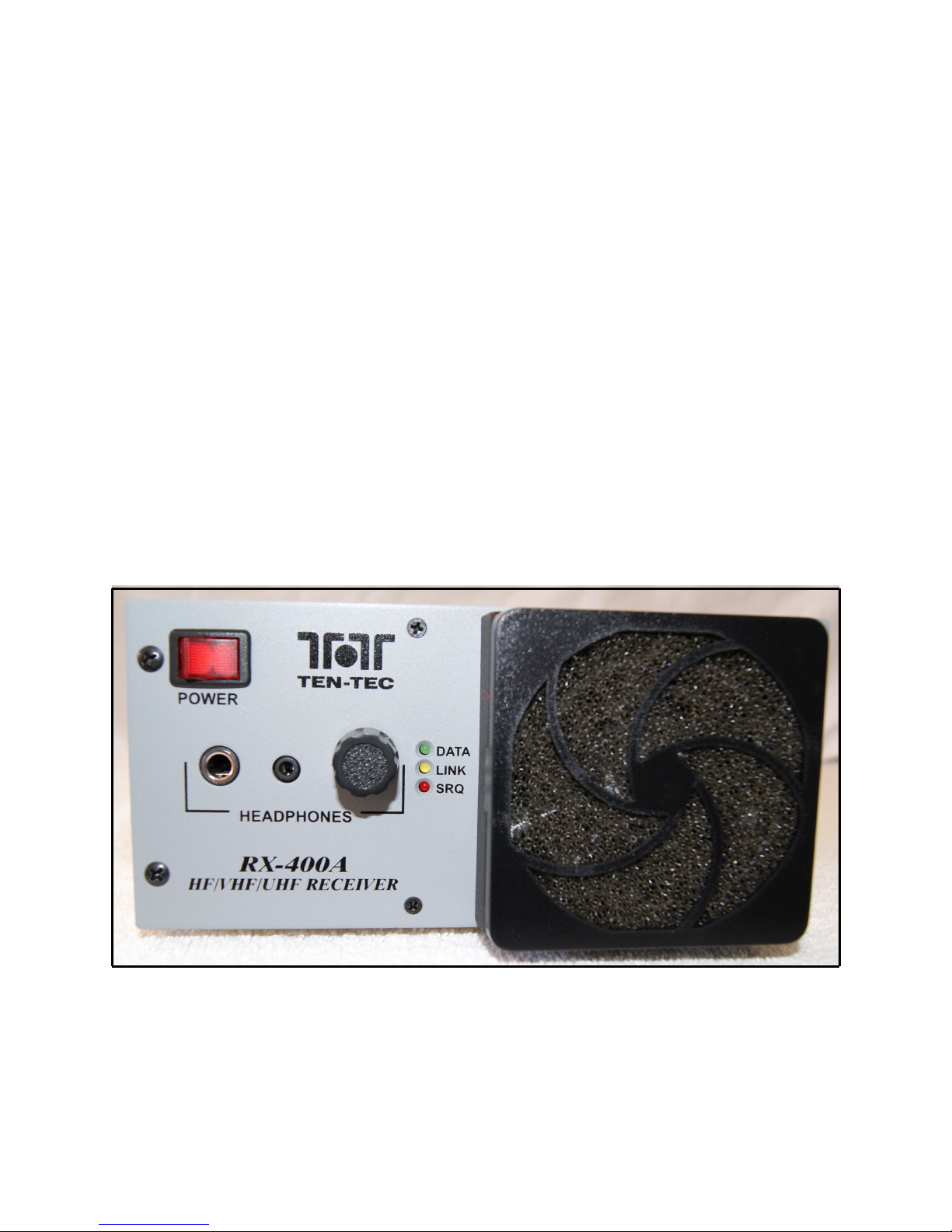
The TEN-TEC RX-400A is an all mode, wide RF coverage, HF/VHF/UHF receiver that
delivers military-grade performance in a Commercial-Off-The-Shelf (COTS) product. The
unit is designed to provide signal acquisition, monitoring and collection functions using
manual tuning, frequency scan or directed search memory channel modes of operation.
The RX-400A covers the frequency range of 100kHz to 3000 MHz using a mix of high
performance analog circuitry for the RF to IF conversion path coupled to a digital backend comprised of the latest digitizer and DSP techniques to provide a software defined
receiver. The DSP section provides 27 digital IF filters from 100Hz to 300kHz and AM,
FM, USB, LSB and CW detection modes. Other than a power ON/OFF switch,
headphone jacks, volume control and status indicators, the receiver has a blank front
panel, thus is designed for remote control operation. Remote control is via a
companion RCU-400A Receiver Control Unit or via a host/PC using an optional Graphical
User Interface (GUI) software package.
All interface to the Receiver is via rear panel connectors for power, RF input, IF outputs,
line audio output, external reference input and remote control. The rear panel also
contains a dip-switch to set the receiver configuration to operational or firmware update
modes.
2-1 PN 74446
Figure 2-1 RX-400A, Front View
Page 10
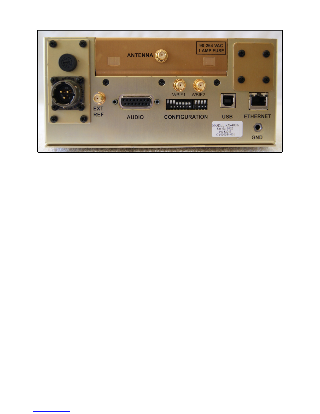
Figure 2-2 RX-400A, Rear Panel View
The RX-400A contains separate signal paths for HF and VHF/UHF frequency bands. The
HF section covers the 100kHz to 88 MHz range. The VHF/UHF front-end covers the
range from 88 MHz to 3000 MHz. A single RF input connector is used to cover both
ranges. Internal firmware commands automatically switch between the HF and
VHF/UHF pre-selector sections based on tuned frequency.
During HF operation signals entering the HF converter section first pass through a user
adjustable step attenuator to enhance receiver performance by reducing interference
caused by receive overload in the presence of extremely large signal levels encountered
in the HF frequency domain. The attenuator is followed by multiple pole RF filters (preselector) to eliminate potential interference from out-of-band signals.
For VHF/UHF operation the received signals are routed to the high band pre-selector
which contains switched filter sets to cover sub-octave ranges between 88 and 3000
MHz. For other than U.S. Government, U.S. Military or approved foreign government
use the RX-400A will not provide coverage of the various cellular telephone bands.
The 2 Receiver IF outputs, WBIF 1 and WBIF 2, provide wideband IF signals for use
with auxiliary analysis equipment such as IF pan signal monitors and IF-Tape
converters. The IF center frequency is 21.4 MHz with a bandwidth of 2 MHz below a
tuned frequency of 20 MHz. From a tuned frequency of 20 to 3000 MHz the IF
bandwidth is 6 MHz.
2-2 PN 74446
Page 11
The RX-400A contains two (2) command and control ports, an Ethernet IP RJ-45
connector, and a standard USB connector. Both interfaces support the same command
set, with the exception of the digital audio streaming which is only available on the
Ethernet IP interface. Generally the USB interface is used as the firmware update port
or for connection to an external host PC for receiver control using the optional GUI
package, while the Ethernet interface is used for connection to the RCU-400A Receiver
Control Unit, for control/status and audio streaming. This port can also be used for
connection directly to a host PC with the added benefit of audio streaming capability,
providing the host has the optional GUI software installed.
Internal RX-400A receiver firmware establishes the operating features and parameters
such as tuned frequency, gain, AGC mode, IF filter bandwidth, detection mode, BFO
and all the functions associated with frequency and memory channel scan modes. This
firmware can be updated in the field using a laptop computer or the system host
PC/workstation with the appropriate drivers. See Chapter 6 for details.
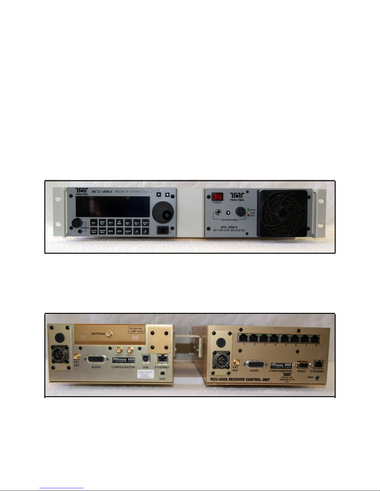
Figure 2-3
RX-400A Receiver Mounted Side-By-Side with RCU-400A Receiver Control Unit
Front View
Figure 2-4
RX-400A Receiver Mounted Side-By-Side with RCU-400A Receiver Control Unit
Rear View
2-3 PN 74446
Page 12

2.2 SPECIFICATIONS
TABLE 2-1
Parameter Performance
Frequency Range……………………………….100 kHz to 3000 MHz
Tuning Resolution………………………………1 Hz steps (10kHz steps at WB IF output)
Operating Modes……………………………… Manual Tune,F1-F2 Scan and Memory
Channel directed search
Detection Modes………………………………..AM, FM, USB, LSB and CW
Frequency Stability…………………………….TCXO, +/-20Hz below 30 MHz,
+/- 0.5ppm above 30 MHz
Frequency Accuracy…………………………..All oscillators locked to int./ext. reference
External Reference…………………………….1,2,5 or 10 MHz @ -10dBm nominal,
receiver automatically switches to this
reference upon application
Spurious Responses…………………………..All spurious less than –105 dBm, equivalent
input max., except with approx. 6 spurs @ less
than –80 dBm
Image Rejection………………………………..80 dB typical, 2-3000 MHz
IF Rejection………………………………………80 dB typical, 2-3000 MHz
BFO…………………………………………………Tunable in CW mode only, +/- 8 kHz in 10 Hz
steps, fixed offset in USB/LSB modes, disabled
in AM, FM modes
Memory Channels…………………………….1000 each, full receiver parameter set-up
Scan Rate………………………………………..100 channels per second or faster, adjustable
Gaze, Dwell and Dead times
Synthesizer Lock Time………………………. Approximately 1 millesecond
Squelch……………………………………………Adjustable, 0-127 dB
Selectivity………………………………………..Std. 27 IF bandwidth set, 100 Hz to 300 kHz,
independent of detection mode, 1.5:1 shape
factor or better, DSP derived, 3 dB ripple, max.
Sensitivity………………………………………..Mode S/N BW dBm
USB/LSB 10 dB 3 kHz -117
AM (50%) 10 dB 6 kHz -108
FM-NB 16 dB 15 kHz -107
FM-WB 16 dB 50 kHz -102
FM-WB 16 dB 200 kHz -96
Dynamic Range………………………………. Freq. NF(typ) In-band IIP (typ)
2-88 MHz 12 dB -2 dBm
89-1650 MHz 13 dB -3 dBm
1651-3000 MHz 14 dB -3 dBm
2nd Order Intercept Point………………….50 dBm, minimum
2-4 PN 74446
Page 13

TABLE 2-1, Cont’d
SPECIFICATIONS
Parameter Performance
AGC…………………………………………………..Fast, Medium, Slow & Programmable, Manual
Gain (MGC) setting provided in all 4 modes,
120 dB range, AGC DUMP in all 4 modes
Mode Attack Hang Decay
Fast 0.8 dB/ms 0 1200 dB/Sec
Medium 0.8 dB/ms 0 100 dB/Sec
Slow 0.8 dB/ms 0 25 dB/Sec
Prog. .01-1.0 dB/ms .01-99.9 .01-99.9
Sec. dB/Sec.
Wideband IF Output…………………………..Analog, 21.4 MHz CF, fixed gain, 6 MHz BW,
10 kHz tuning steps, 2 MHz BW below 20 MHz
receiver tuned frequency
S-Meter……………………………………………..Reports signal level to host in dBm on request
Control Interface(s)……………………………2, Ethernet TCP/IP (RJ-45), and USB, std. 2.0
Firmware…………………………………………..Can be updated remotely into Flash ROM
Antenna (RF) Input…………………………….50 ohms, unbalanced, SMA connector, 2.5:1
VSWR max.
Line Audio Output(s)..…………………………2 each, 0 dBm, +/- 3 dBm, 600 ohms, One
AC coupled, one DC coupled, 15 pin-D
Headphone(s) Output………………………….2 stereo jacks, one std ¼ inch, one std. 1/8,
10 mW into 600 ohms, front panel volume
control
BITE………………………………………………….Reports pass/fail status to host on request
MTTR………………………………………………..Less than 30 minutes for replacement of any
of 9 major sub-assemblies
PN 74446
2-5
Page 14

2.3 ENVIRONMENTAL CONDITIONS
The RX-400A Receiver is a rugged design intended for commercial, government and
military applications. The unit is specifically suitable for fixed site, vehicle or shelterized
installations, shipboard service and cabin-class turbo-prop/jet aircraft if appropriate
shock and vibration isolation is provided. The RX-400A is a COTS product and as such
is not certified to MIL-STD-810 standards, however the unit is designed to meet shock
and vibration levels associated with procedure 514 for cabin-class aircraft environments.
With regard to RFI/EMI the RX-400A is designed to meet, although not factory tested,
to MIL-STD-461F for CE02, CE03, RS01, RS02 and RS03.
The RX-400A is designed to operate under the conditions in Table 2-2.
TABLE 2-2
ENVIRONMENTAL CONDITIONS
Parameter Specification
Operating Temperature……………………………..0 to 50 degrees C, full specification
Operating Limits……………………………………….Functional, -10 to +60 degrees C
Storage Temperature………………………………..-40 to +85 degrees C
Humidity…………………………………………………..10-95%, without condensation
Altitude…………………………………………………….+15,000 feet MSL, un-pressurized
2.4 MECHANICAL
The RX-400A Receiver is housed in a standard 2U high EIA half-rack chassis. It has a
behind the panel depth of 16.00 inches (407mm), excluding connectors.
Construction is all aluminum with wrapped corners and a thick front panel to
accommodate rack mounting. Top and bottom covers are affixed using flat head
screws. 10-32 threaded inserts are installed in the chassis sides to accommodate user
slides. The rear panel has a 10-32 threaded insert to accept a chassis ground
connection. The chassis is chem.-treated to resist corrosion and the front panel is
painted gray with black silk screening.
The RX-400A weighs 10.25 lbs. (4.65 kG)
Figure 2-5 depicts a 3-view drawing for the RX-400A Receiver.
2-6 PN 74446
Page 15
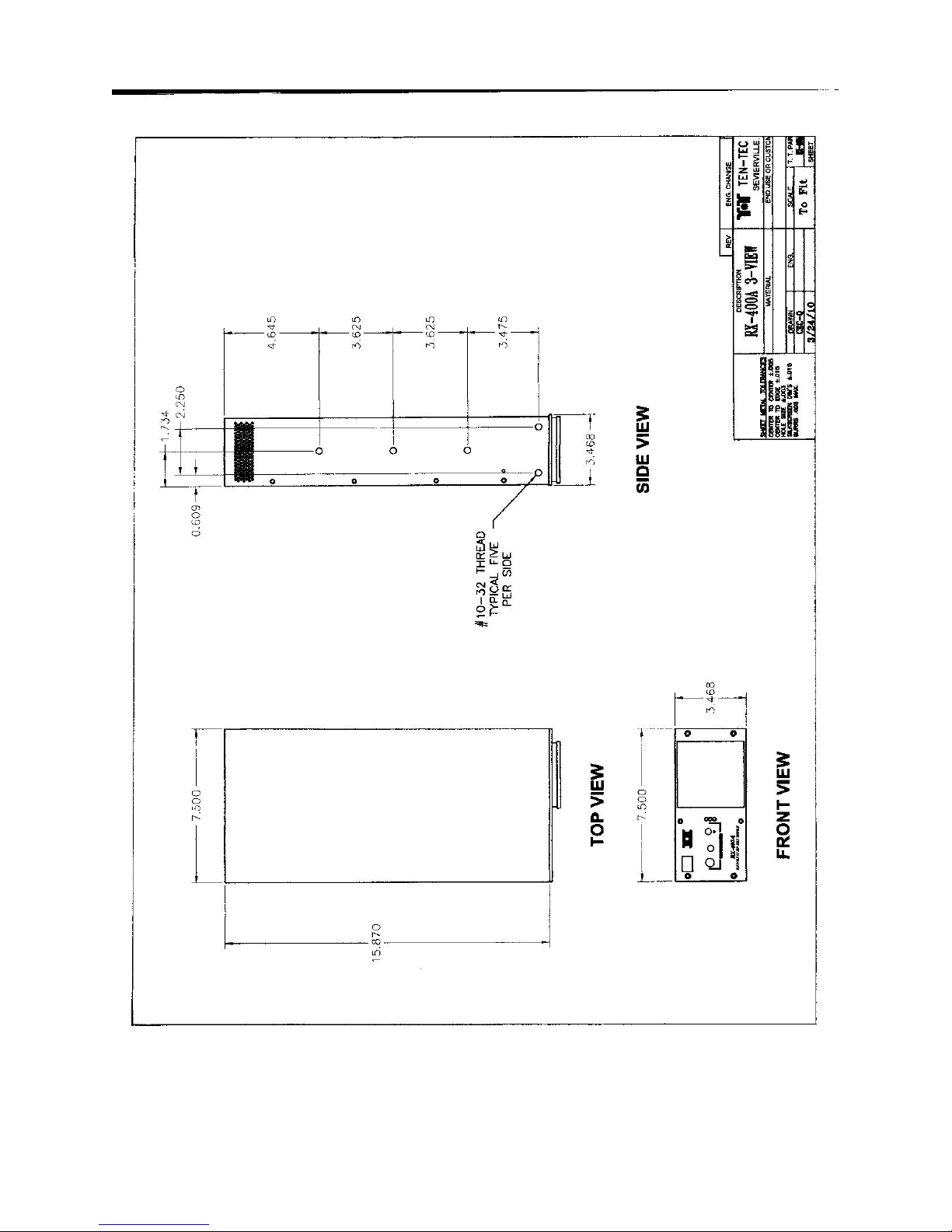
FIGURE 2-5 RX-400A RECEIVER, 3-VIEW DRAWING
PN 74446
2-7
Page 16
2.5 ELECTRICAL
Power requirements for the RX-400A are presented in Table 2-3.
TABLE 2-3
RX-400A POWER REQUIREMENTS
Parameter Specification
Line Voltage……………………………………………..90 to 264 VAC
Frequency………………………………………………..48-440 Hz, single phase
Power Consumption………………………………….36 Watts, nominal
Power Connector.……………………………………..Circular MS type connector, 3-pin, male
Spikes and Noise……………………………………….Designed to meet MIL-STD-704,
but not tested at factory
Power Connection……………………………………..Pin-A, AC High; Pin-B, AC Low; Pin-C,
AC Ground
Phones 1
Phones 2
Status Indicators
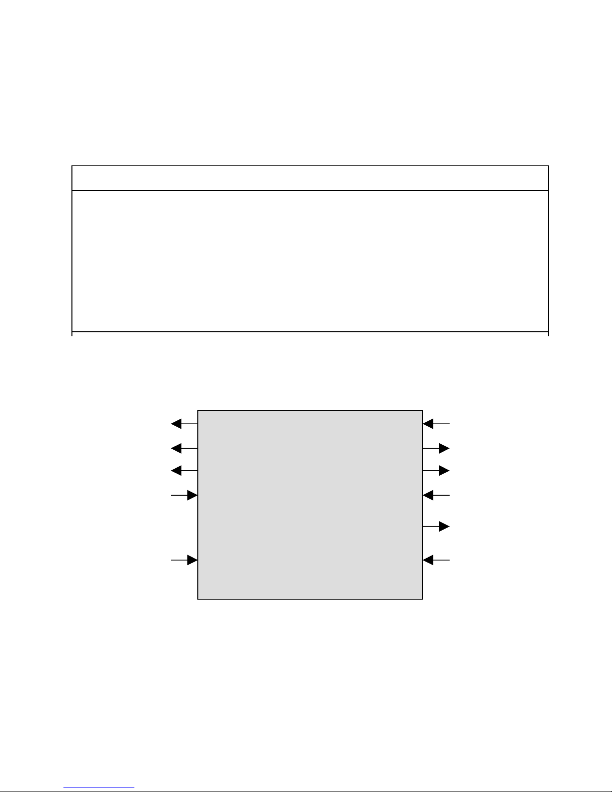
RX-400A HF/VHF/UHF
RECEIVER
Volume Control
Power Switch
FIGURE 2-6 RX-400A ELECTRICAL INTERFACE
2-8
3.0 PREPARATION FOR USE AND INSTALLATION
RF Input 100kHz-3000MHz
IF 1, 21.4 MHz
IF 2, 21.4 MHz
External Reference
Line Audio
90-260 VAC Power
PN 74446
Page 17
3.1 UNPACKING AND INSPECTION
Examine the shipping carton for damage before unpacking the unit. If the carton is
damaged, attempt to open it in the presence of the shipping agent. If this is not
possible then document or photograph the carton damage for a matter of record. If
undamaged then retain the carton and packing material for future use.
Remove the packing material from the top of the unit and lift the RX-400A Receiver free
of the carton. Next remove the clear plastic bag from the unit. Inspect the unit for
external damage with particular attention to dents or bent sheet metal. Also inspect
front panel components and rear panel connectors for damage. If external damage is
evident then remove top and bottom covers of the RX-400A Receiver by removing
multiple screws along the cover edges, then inspect all the internal assemblies for
damage such as cracked circuit cards or broken or loose components. DO NOT
ATTEMPT TO OPERATE THE EQUIPMENT IF INTERNAL DAMAGE IS NOTED. Upon
finding any damage contact the shipping agent and contact the TEN-TEC factory to
arrange for unit repair.
3.2 MOUNTING
The RX-400A may be mounted as a single unit or side-by-side with another 2U half-rack
piece of equipment in a standard EIA 19” rack enclosure. For single unit rack
installation please contact TEN-TEC to secure the correct rack mount kit. For most
common mounting arrangements the RX-400A will be installed side-by-side with
another RX-400A Receiver or companion RCU-400A Receiver Control Unit to fill a 2U
rack opening. Side-by-side mounting is accomplished by using the RM-400-2 Rack
Mount Kit. The RX-400A has 3 threaded inserts on each side of the chassis to accept
10-32 x 0.50” long screws for use with customer furnished chassis slides. The hole
pattern is compatible with Jonathan model 375QD or equivalent.
The rack mount kit contains 4 pieces as listed in Table 3-1.
Item Description Quantity
001 U-Channel Bracket 1
002 Front Panel Center Bracket 1
003 Rack Mount Ears (R & L) 2
004 10-32, Hex Head Attachment Screws 12
To use the RM-400-2 rack mount kit, first attach the U-channel bracket to the ‘inside’
side of one of the chassis using the rear 2 mounting holes out of the set of 3, with the
furnished screws. Then attach the front panel bracket to the chassis with the flat side
TABLE 3-1
RM-400-2 Rack Mount Kit Contents
3-1 PN 74446
Page 18

toward the front panel surface. Next, position the second chassis so the U-channel and
front panel brackets can be attached to the second chassis. Now the 2 units are
secured together with about a 2 inch gap between the chassis. Next attach the left
hand and right hand brackets (rack mount ears) using the furnished screws. The ears
are attached using 2 threaded 10-32 inserts at the front of the RX-400A chassis. Refer
to Figure 3-1 for parts orientation.
3.3 POWER
Ensure the Power Switch is in the OFF position on The RX-400A Receiver (left side of
switch depressed toward front panel). Connect a customer furnished power cable with
a female MS-type 3-pin plug to the power connector on the rear of the RX-400A. Pin
wiring for the cable must be identical to that listed in Table 2-3. Next plug the other
end of the cable into a 90-260 VAC, single phase power source.
3.4 RF, IF, EXTERNAL REFERENCE AND AUDIO CONNECTIONS
The RF (Antenna) connection is made to Receiver via a SMA connector. Both WBIF
outputs are connected to external devices using SMA connectors/cables. Likewise an
external reference signal can be connected with a SMA cable. Balanced Line Audio is
available on a rear panel 15-pin D connector where connections are made via a
customer furnished mating connector and cable assembly. Pin assignments are listed in
Table 3-2.
3.5 REMOTE CONTROL CONNECTION
RX-400A Receiver control is via two (2) interface connectors on the rear panel. One is
a USB 2.0 interface using the standard USB type connector. The other is ETHERNET
using a RJ-45 type jack. Either interface can be used to control the receiver and the
command sets are identical, however, only the ETHERNET interface provides the digital
audio streaming capability. Please see Chapter 7 for detailed information for command
words.
3.6 CONNECTION TO THE RCU-400A RECEIVER CONTROL UNIT
For operator manual control of the Receiver it can be connected to a companion RCU400A Receiver Control Unit, either co-located with the Receiver or at a different position
from that of the Receiver. In this case use the ETHERNET interface on the Receiver
and connect a cable to port 1 through port 7 on the RCU-400A.
PN 74446
3-2
Page 19
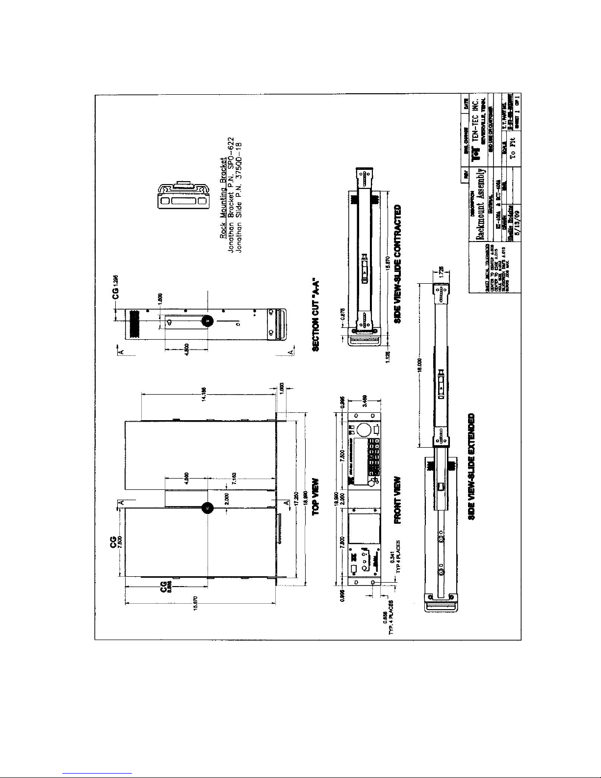
FIGURE 3-1 RX-400A and RCU-400A INSTALLATION
PN 74446
3-3
Page 20
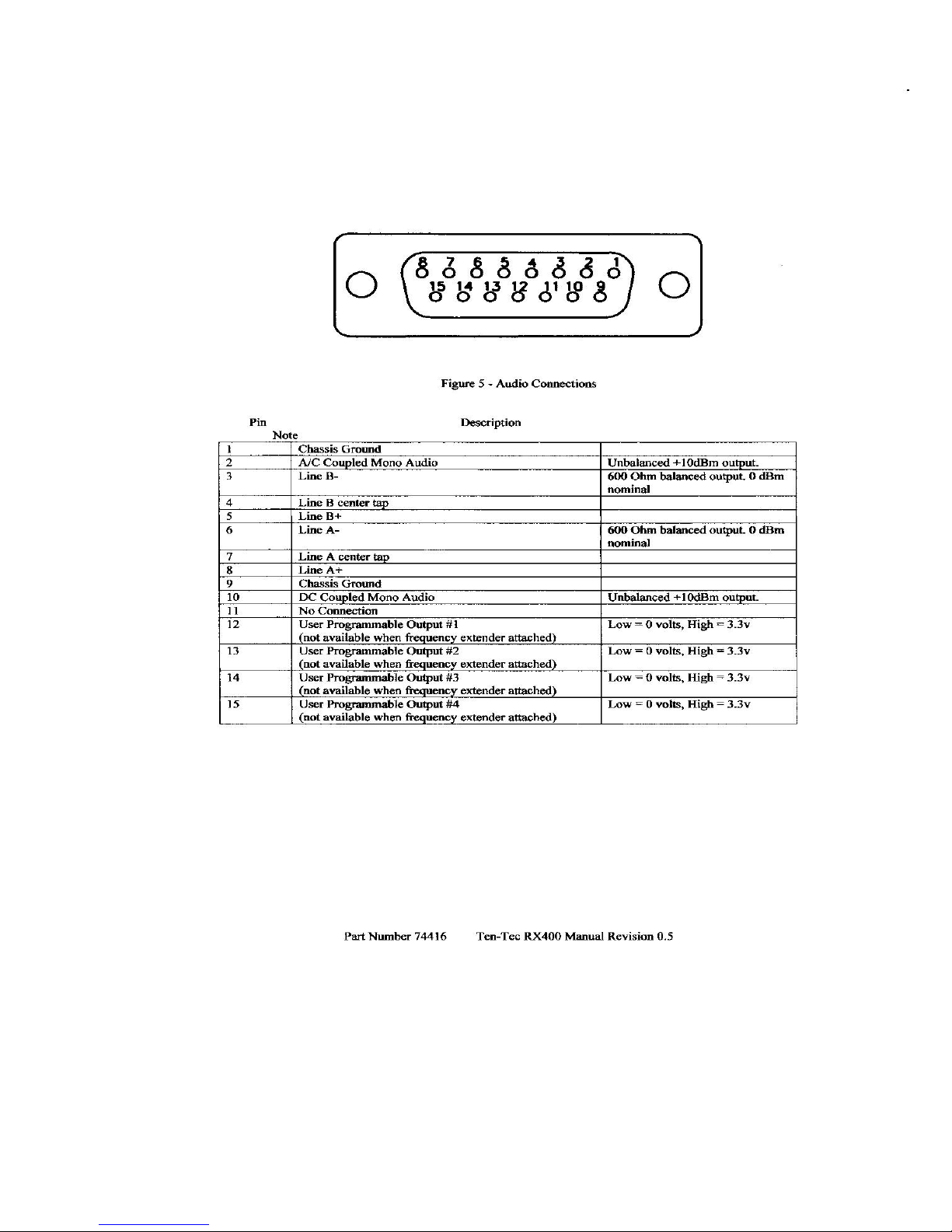
TABLE 3-2
RX-400A AUDIO CONNECTIONS
PN 74446
3-4
Page 21
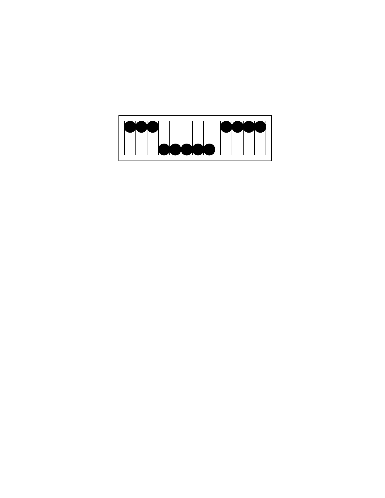
3.7 CONFIGURATION DIP SWITCH
The rear panel contains a recessed two section Dip Switch used to set the operating
configuration for the Receiver. The first section contains 8 switches and the second
contains 4 switches. For normal Receiver operation, place the first section with
switches 1, 2 and 3 in the UP position and 4 through 8 in the DOWN position. All four
switches (1 through 4) are placed in the UP position for the second switch section.
1 2 3 4 5 6 7 8 1 2 3 4
3.8 FUSE
A replaceable fuse is located above the power connector on the rear panel. The fuse is
removed and replaced using a small (1/8”) wide common blade screwdriver. Replace it
with a 5x20 mm, 1 Amp, 250VAC, time delay fuse.
3.9 FRONT PANEL CONTROLS
The RX-400A is designed for remote operation so the front panel controls are limited. A
switch is provided to control the unit power ON/OFF.
3.10 HEADPHONE JACKS
Two headphone jacks are provided, one for 1/4 inch, and one for 1/8 inch stereo plugs.
3.11 FRONT PANEL INDICATORS
The power switch has a built-in indicator that glows red when the unit is turned ON.
Data, Link and SRQ LEDS are provided to provide the status of the Receiver.
3.12 COOLING FAN
A quiet running fan/filter assembly is mounted to the front panel to provide cooling air
flow to the Receiver.
3.13 CHASSIS GROUND
A chassis ground connection should be made on the rear panel using a 10-32 x ½ inch
screw and terminal lug. The ground wire should be AWG #16 or larger.
PN 74446
3-5
Page 22

4.0 OPERATION
Since the RX-400A is intended for remote control, operation is limited to power
ON/OFF, audio volume control and viewing of status indicators. It is assumed the
Receiver will be connected to either a RCU-400A Receiver Control Unit or host PC using
the optional Graphical User Interface (GUI) software package. Connections are to be
made per paragraphs 3.5 and 3.6.
4.1 POWER ON/OFF
The Receiver power is turned ON by depressing the right side of the toggle switch
toward the front panel. A built-in red lamp will illuminate to indicate power has been
applied.
4.2 HEADPHONES VOLUME
The headset audio level may be adjusted by rotating the VOLUME control, minimum at
full CCW position, full volume at full CW position.
4.3 STATUS INDICATORS
Three LED indicators are provided to indicate the operating status of the Receiver. The
green DATA LED blinks or is on-steady when data is being transferred to/from the
Receiver to the RCU-400A Receiver Control Unit or host PC. The yellow LINK LED is on
when the link between the Receiver and an external device has been established. The
SRQ LED illuminates when service requests are received.
Refer to Figure 2-1 for the Receiver front panel component locations.
NOTES
1.Full receiver operation descriptions for Manual Tuning, F1-F2 Frequency Scan and
Memory Channel Scan modes as well as other control parameters such as Gain Control,
Squelch, Bandwidth, Detection Mode, BFO and AGC is provided in the RCU-400A
Receiver Control Unit User Manual
2. Directed Search, using host workstation loaded optional software package, provides
Mission Download capability via the RCU-400A Receiver Control Unit
PN 74446
4-1
Page 23
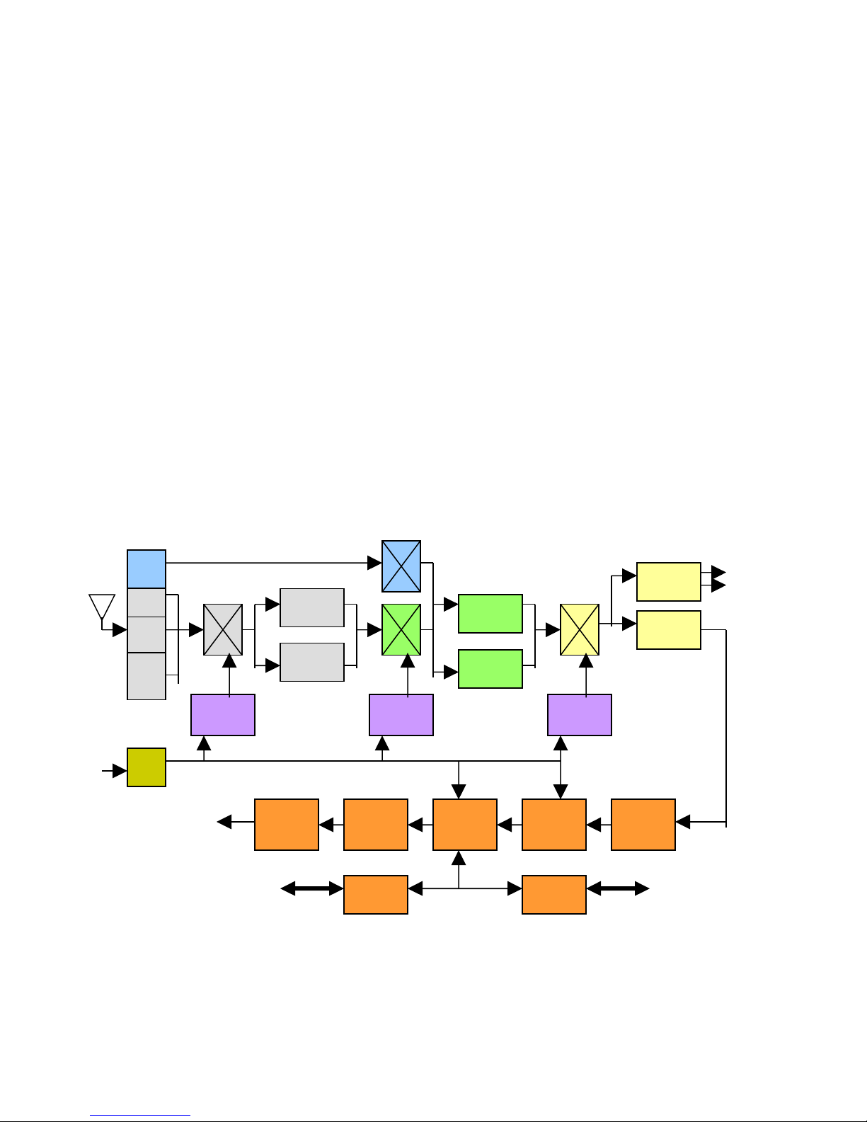
5.0 THEORY OF OPERATION
nverter
5.1 OVERVIEW
The Ten-Tec model RX-400A is a DSP-based receiver with a wide-band IF output
available at 21.4MHz. The superhetrodyne architecture is triple-conversion to the IF
output for received frequencies of 88 MHz to 3GHz, and double conversion when tuned
below 88 MHz. The IF output bandwidth is 6 MHz for tuned frequencies of 20 MHz to 3
GHz, and 2 MHz when tuned below 20 MHz receive frequency. Tuning step size is 10
kHz (1 kHz optional) at the 21.4 MHz IF output. Conversion gain from antenna to IF
output is 3 dB nominal. The block diagram in Figure 5-1 outlines the signal path and
major functions throughout the RX-400A architecture.
The 21.4 MHz 3rd IF is bandpass filtered to 300 kHz bandwidth in the 3RD CONVERTER
module, AGC leveled, and presented to the DSP board. On the DSP board, a high-speed
A/D converter drives an AD6620 Digital Down Converter which applies fine tuning,
further bandpass filtering, and decimation to the digitized IF signal to prepare the data
for a Digital Signal Processor. Final selectivity filtering and mode-specific detection
functions are accomplished by the DSP.
Audio/Video outputs are available via connectors on either rear or front panel. The
outputs are designed for a nominal 600-ohm load.
HF Converter
Second Converter
BPF 6 MHz
BW
140 MHz
BPF
BPF
RF Input
Low Band
Mid 1
Mid 2
First Converter
4090 MHz
BPF
2528 MHz
WBIF 1
WBIF 2
High
Preselector
Ref.
Ext. Ref.
BPF
1st LO 2nd LO 3rd LO
AUDIO
COMMAND &
STATUS DATA
Reconstr.
USB Interface ETHERNET
BPF 2 MHz
BW
950 MHz
FIGURE 5-1 RX-400A BLOCK DIAGRAM
5-1
DDC DSPD/A CONVANALOG
Interface
Third Converter
117-119
MHz
A/D
CONV
COMMAND &
STATUS DATA
21.4 MHz IF2528-4090 MHz 2300 MHz
PN 74446
Page 24

Six modules located on the bottom chassis deck accomplish the analog frequency
conversion functions. These interconnected modules are the FIRST, SECOND, and
THIRD CONVERTERS and the FIRST, SECOND, and THIRD LOCAL OSCILLATORS.
Signal interconnection between modules is by miniature semi-rigid coax.
Two interconnected PRESELECTOR BOARDS located on the top foldout chassis deck
perform frequency band pre-selection and signal pre-amplification between the antenna
input and the FIRST CONVERTER module.
The DSP BOARD located on the inner chassis deck performs all digital signal
conditioning, detection algorithms, and logic control functions. The DSP BOARD also
contains the audio/video output amplifiers and the TCXO master frequency reference.
Distribution of control signals and power to the various radio modules and boards is via
connectorized ribbon cable between the DSP BOARD and the target board/module.
All DC power is supplied by a shielded universal AC input switching supply located on
the inner chassis deck. The DSP BOARD receives the outputs from this main power
supply for post-regulation and distribution to the other radio modules.
A front-mounted fan supplies forced-air ventilation. Cooling air enters at the frontmounted filter and exits through vent holes around the rear perimeter of the chassis.
The front panel board provides both high-speed and low-speed fan connections. To
change fan speed from fast to slow, see paragraph 9.5 of this manual.
5.2 CIRCUIT DESCRIPTIONS
The rear panel antenna input is protected by a spark gap and filtered by a 3 GHz lowpass filter on the MID/HIGH BAND PRESELECTOR board, then routed to the common
terminal of a 4-position switch. Below a 88 MHz receive frequency the RF signal from
the antenna is connected to the LOW BAND PRESELECTOR board, either directly or
through a 20 dB resistive pad.
5.2.1 Low Band Preselector
Dual PIN diodes on the LOW BAND PRESELECTOR select one of eight sub-octave
bandpass filters. Each of the eight filters selects a frequency band approximately 2/3
octave wide to cumulatively cover the Low Band range of 2 to 88 MHz (slightly over 5
1/3 octaves). After bandpass filtering, the selected fractional-octave band is amplified
by and passed through a 140 MHz band-reject filter. This band-reject filter provides
additional attenuation of the Low Band 1st IF frequency. Buffers pass serial data to a
PIN diode driver Commands enables power to the RF preamplifier.
PN 74446
5-2
Page 25

5.2.2 Mid/High Band Preselector
Position 3 of the switch on the MID/HIGH BAND PRESELECTOR board routes the
antenna signal through a bank of seven mid-band filters selected by switches. Logic
lines determine complimentary switch positions. The first mid band filter is dedicated to
the US FM broadcast band of 88-108 MHz. The remaining six filters have approximate
2/3 octave pass-bands to cover 108 to 1650 MHz. The selected filter output is
amplified and low-pass filtered, then routed to the Mid Band / High Band switch.
Position 4 on the MID/HIGH BAND PRESELECTOR board routes the High Band antenna
signals through one of two high-pass/low-pass filter cascades selected by switches.
Complimentary switch positions are determined by a logic line. This arrangement
creates two half-octave sub-bands of 1650-2200 MHz and 2200-3000 MHz. The
selected portion of the High Band is further conditioned by an amplifier and high-pass
filter before being presented, along with the Mid Band sub-band to a switch. Based on
a logical AND combination, the switch routes the selected sub-band through another
amplifier to the MID/HIGH BAND PRESELECTOR board output.
5.2.3 First Converter
The FIRST CONVERTER module contains the first mixer and first IF amplifier for all
receive frequencies above 88 MHz. The first local oscillator, moving in 2 MHz steps
from 2528 to 4090 MHz, is high-pass filtered, then amplified and applied as high side
injection to the first mixer. On the Mid Band receive frequencies of 88-1650 MHz, the
mixer produces a 2440 MHz first IF which is filtered and amplified by the cascade first
IF filters. This 2440 MHz IF has approximately 80 MHz bandwidth determined by SAW
filters.
On the High Band receive frequencies of 1651-3000 MHz, the first mixer produces a
1090 MHz first IF filtered and then amplified. The 1090 MHz IF has approximately 14
MHz bandwidth determined by two dielectric filters.
5.2.4 Second Converter
The SECOND CONVERTER module contains the second mixer for all receive frequencies
above 88 MHz. It also contains the first mixer for receive frequencies below 88 MHz.
Each mixer, selected by a switch, drives a common 140 MHz IF amplifier. Switches
select an IF filter of either 6 MHz bandwidth for receive frequencies above 20 MHz, or 2
MHz bandwidth for use below 20 MHz.
PN 74446
5-3
Page 26

The input Mid Band and High Band first IF frequencies of 2440 or 1090 MHz are mixed
with fixed Second LO injection frequencies of 2300 or 950 MHz respectively. Each
injection signal is provided by the SECOND LOCAL OSCILLATOR module, which is
filtered and amplified, then applied to the LO port of the mixer.
On Low Band, the LOW BAND PRESELECTOR board supplies the100 kHz-88 MHz signal
to the RF port of HF Mixer. The Low Band injection signal is developed in the FIRST
LOCAL OSCILLATOR module by dividing a 2272-3648 MHz VCO by 16 to produce 142228 MHz in 250 kHz steps. This frequency-divided first LO is routed through the FIRST
CONVERTER module then applied to the LO port of the HF mixer.
The 140 MHz IF output from a switch is low-pass/high-pass filtered, then amplified and
routed to the THIRD CONVERTER module.
5.2.5 Third Converter
In the THIRD CONVERTER module, the third mixer is for receive frequencies above 88
MHz (Mid/High bands) and acts as the second mixer for receive frequencies below 88
MHz (Low Band). The LO injection signal, developed in the THIRD LOCAL OSCILLATOR
module, tunes a 2 MHz range from 117.71 to 119.7 MHz in 10 kHz steps (1 kHz
optional). Low Band receive frequencies use a 240 kHz segment of this range from
118.48 to 118.72 MHz to fill in the 250 kHz tuning steps produced by the divided-down
first LO. The third LO injection signal is amplified and applied to the LO port of the
mixer. A 159 MHz trap attenuates a potential image frequency response.
The 21.4 MHz IF resulting from this low-side mix provides two outputs from the THIRD
CONVERTER module: The Wideband IF Output is sampled by a directional coupler and
then low-pass filtered. This output is either 2 MHz or 6 MHz wide, depending on the
receiver tuned frequency, and has 10 kHz (1 kHz optional) tuning resolution. The
Narrowband Output is filtered to 300 kHz bandwidth, amplified and AGC leveled, then
delivered to the DSP BOARD.
Double-resonator filters along with an amplifier provide a 21.4 MHz tuned IF stage
which delivers a 300 kHz sub-band of the mixer output to a variable gain amplifier.
Additional fixed gain amplifiers boost the signal to a maximum of 1 volt peak-to-peak
which is then low-pass filtered before being fed to the AGC detector.
A balanced diode detector samples the IF signal at the output of an amplifier and
provides a rectified signal envelope to the AGC amplifier. Components in the AGC loop
determine the circuit time constants. Buffers for the AGC node voltage complete the
AGC loop. The active region of the VGA control input is 0.25 to 1.5 volts with a positive
slope of 32 dB/V establishing a 40 dB control range.
PN 74446
5-4
Page 27

A Manual Gain Control buffer and window comparator provide a means for the DSP
processor to modify the analog AGC function. When a digital-to-analog converter on
the DSP BOARD reduces the MGC voltage below the existing analog AGC voltage,
feedback regulates the AGC voltage to the new set value. The ANALOG and DIGITAL
outputs inform the DSP which driving source is asserting analog AGC gain reduction,
the analog envelope detector or the digital-to-analog converter. This mechanism allows
software implementation of both manual gain control and slower analog AGC decay
rates.
Another function enabled by this circuit arrangement, useful in narrowband detection
modes, is DSP correction of analog AGC action caused by strong signals located outside
the digitally implemented selectivity bandwidth. Because the analog AGC detector
samples the entire 300 kHz analog IF bandwidth, some signals causing AGC action may
be invisible to the DSP when narrow selectivity filtering (partially implemented in a
AD6620 Digital Down Converter) precedes the digital detection algorithm. The
information provided to the DSP by the AGC, ANALOG, and DIGITAL outputs allow the
software to identify and compensate for the effects of these strong "out-of-band"
signals. As a result, signal strength calculation and overall AGC action is based only on
those signals that are inside the chosen selectivity bandwidth. Fast, Medium and Slow
AGC modes with fixed, pre-determined, attack and decay times are provided, along with
a Programmed AGC mode where the operator can select the attack, hang and decay
times in milliseconds.
5.2.6 First Local Oscillator
The FIRST LOCAL OSCILLATOR module contains a single-loop fractional-N frequency
synthesizer producing 2272-4090 MHz in 2 MHz steps. Serial data from the DSP board
configures synthesizer to divide the provided 100 MHz reference by five and the
selected VCO by a MODULO 10 fractional N-number of 113.6 to 204.5 for phase
comparison. Integrated phase pulses from the synthesizer chip develop a DC tuning
voltage for the active VCO. The tuning voltage output is sampled and delivered to the
DSP board for possible charge pump gain calibration based on VCO tuning voltage slope
variation. A loop filter reduces reference and phase-correction ripple on the tuning
voltage before it is applied to the VCO control input. The active VCO output selected by
a switch splits to two buffer amplifiers. One amplifier provides feedback to the
synthesizer chip, completing the loop. The second amplifier develops the Mid/High
Band First LO output which splits between the module output and MODULO 16 divider
to provide the Low Band First LO of 142-228 MHz.
The 100 MHz master frequency reference signal is developed on the DSP board and is
delivered through this module to the SECOND LOCAL OSCILLATOR module.
PN 74446
5-5
Page 28

5.2.7 Second Local Oscillator
The SECOND LOCAL OSCILLATOR module contains a single-loop fractional-N frequency
synthesizer producing a fixed frequency of 2300 or 950 MHz. Serial data from the DSP
board configures the synthesizer to divide the provided 100 MHz reference by 5 or 10
and the selected VCO by a MODULO 10 fractional N-number of 115.0 or 95.0 for phase
comparison. Integrated phase pulses from the synthesizer chip develop the DC tuning
voltage for the active VCO. A loop filter reduces reference and phase-correction ripple
on the tuning voltage before it is applied to the VCO control input. The active VCO
output selected by a switch that drives the module output through a buffer amplifier.
A sample of the output provides feedback to the synthesizer chip, completing the loop.
The 100 MHz master frequency reference signal from the FIRST LOCAL OSCILLATOR
module is delivered through this module to the THIRD LOCAL OSCILLATOR module.
5.2.8 Third Local Oscillator
The THIRD LOCAL OSCILLATOR module contains a single-loop integer-N frequency
synthesizer driving an N=1 mixing loop to develop a 117.71 to 119.7 MHz output tuning
in 10 kHz (or optionally 1 kHz) steps.
Serial data from the DSP board configures the synthesizer to divide the provided 100
MHz reference by 250 (or optionally 2500) and VCO by 1771 to 1970 (or optionally
17701 to 19700). Additional circuitry modifies the (nominally 400 kHz) loop filter for
the optional 40 kHz reference frequency when the fine tuning option is selected.
The VCO delivers 708.4 to 788 MHz in 400 kHz (or optionally 40 kHz) steps to the RF
input of the PLL which is programmed to divide by 40 producing a 17.71 to 19.7 MHz
reference in 10 kHz (or optionally 1 kHz) steps at the phase comparator. A VCO
driving buffer develops the module output. The mixing loop is closed via a mixer which
subtracts 100 MHz from the VCO output of 117.71 to 119.7 MHz to provide 17.71 to
19.7 MHz directly to the phase comparator (R=1) through a low-pass filter.
When the receiver is tuning the Low Band (2-88 MHz), the Third LO output frequency is
restricted to the range 118.48 to 118.72 (or optionally 118.471 to 118.720) to fill in the
250 kHz stepping of the divided-down First LO.
PN 74446
5-6
Page 29

5.2.9 Logic/DSP System
The RX-400A Logic/DSP assembly incorporates Digital down Conversion, Signal
Processing, Control & Interface, Power and Master Clock Reference circuitry on a single
circuit board. The Logic/DSP board controls all Preselector, RF Converter and Local
Oscillator (LO) boards over ribbon cables. The RF/LO and Preselector boards are
programmed by the DSP processor via the attached ribbon cables to achieve the correct
RF tuning. In addition, the DSP board monitors LOCK DETECT (LD) signals from the LO
boards to be reported to the controller as status information.
The processor is an Analog Devices ADSP-21364 DSP processor. The DSP processor
communicates with various other on-board components to implement a unified signal
processing and control system. In addition top the DSP processor the system includes
an Analog Devices AD6620 digital down converter. a 16C500 RS-232 UART, 10/100
Ethernet interface chip, FLASH memory components, an A/D and a D/A. System bus
management and I/O are contained in a Xilinx Programmable Logic Device (PLD).
An AD6620 down-converter accepts the 3rd IF signal via a coax connector. The 3rd IF
center frequency is 21.4 MHz. The Digital down Converter (DDC), comprised of two A/D
converters, converts the signal to base band for further processing inside the DSP. The
sample rate between the AD6620 and the DSP is dependent on the selected IF
bandwidth. During power-up the DDC is initialized via its parallel control interface. After
initialization of the DSP processing system the DDC is controlled via the serial control
interface.
The DSP processor provides user control through USB or Ethernet Interfaces. Digital
audio is provided on the Ethernet Interface only. Please see the RX-400A Control
Interface Command Set in Chapter 7 of this manual for command interface details.
5.2.10 Power
The system power supply delivers +/-12V and +/-5V to the Logic/DSP board via an onboard connector. On-board power regulators provide the proper +1.2 and +3.3 volt
supply for the DSP core and I/O system. Additional regulators develop +24 and +9
volts which are provided to other boards via the same ribbon cables which provide
control and monitoring. A connector provides a user-selectable +5 or +12 volts for the
cooling fan depending on application requirements.
PN 74446
5-7
Page 30

6.0 FIRMWARE LOAD AND UPDATE PROCEDURES
6.1 INTRODUCTION
The RX-400A Receiver is delivered from the factory with operating firmware installed.
While the firmware is the latest version available at time of manufacture, updates may
become available at the time of Receiver installation or periodically over the life of the
equipment.
Firmware is available from the TEN-TEC, Inc. by contacting the factory.
6.2 REQUIRED APPLICATION TOOLS
To load firmware updates into the RX-400A Receiver requires the TEN-TEC Flash
Update Utility tool. This tool is available by contacting the factory. Upon receipt load
the utility onto the desktop screen of the laptop or PC. This update utility will run on
Windows 2000, XP or Vista operating systems.
The RX-400A firmware updates are loaded via the Receiver’s USB port. Loading the
firmware requires a USB-to-Serial-Converter driver installed in the laptop or PC being
used to perform the download. This driver is available on the Internet at
FDTIchip.com. Click on ‘Drivers’ and select VCP Driver version 2.0-6.00. Download and
install this driver into the laptop or PC.
6.3 FIRMWARE LOAD/UPDATE STEPS
To load firmware into the RX-400A Receiver perform the following steps:
1. Turn RX-400A power to OFF.
2. With reference to paragraph 3.7 of this manual, place the #1 switch of the left
hand Configuration Dip Switch section to the ‘down’ position.
3. Connect a USB cable from the Receiver USB connector to a USB port on the
laptop or PC.
4. Turn the Receiver power ON.
5. Click and open the Update utility icon on the laptop or PC desktop.
6. Click ‘Settings’, then click ‘Setup’.
7. On the setup window ‘check’ the serial port box.
8. Select the COM port you want to use.
9. Note the IP address, UDP port and radio pass-code entries.
10. Click OK. PN 74446
6-1
Page 31

Firmware Load/Update Steps (cont’d)
11. Now click ‘Process’ on the Flash Utility window.
12. Click on ‘Update Radio’.
13. A ‘select Firmware Update File’ window appears.
14. Select ‘Look In:’ Desktop.
15. Scroll down through the listing until the desired ‘*ruf’ file is located.
16. Highlight the file, then click ‘Open’
17. The load preamble text will be displayed, then the ‘Erase’ steps will occur and
the firmware will then load 4096 lines of new firmware code.
18. Upon completion of download a ‘successfully loaded’ window will appear.
19. Close the application.
20. Place the Receiver power to OFF.
21. Disconnect the USB cable.
22. Return the #1 configuration switch to the ‘UP’ position.
23. Turn Receiver power ON. This concludes the firmware update procedure.
PN 74446
6-1
Page 32
7.0 RECEIVER REMOTE CONTROL
7.1 INTRODUCTION
This chapter describes the RX-400A control interfaces and the associated command set.
All features of the Receiver are controllable through the interfaces. In addition, the
Ethernet interface provides audio streaming from the receiver to a RCU-400A Receiver
Control Unit or PC or any device that can process variable sample rate PCM data
delivered via UDP packets.
7.2 USB INTERFACE DESCRIPTION
The RX-400A Digital HF/VHF/UHF Receiver has the built-in capability of being controlled
remotely by a computer or other controller that is equipped with a USB interface or an
Ethernet port and capable of transmitting and receiving ASCII-standard encoded characters.
A baud rate hardware configuration can be selected via switches 2 and 3 of the
Configuration DIP switch.
The USB interface of the RX-400A is physically implemented on a rear panel standard
USB connector. This interface has a full duplex operation, meaning that it can transmit
and receive data simultaneously.
The baud rates are selectable via configuration dip switches SW2 and SW3. Refer to
Table 7-1.
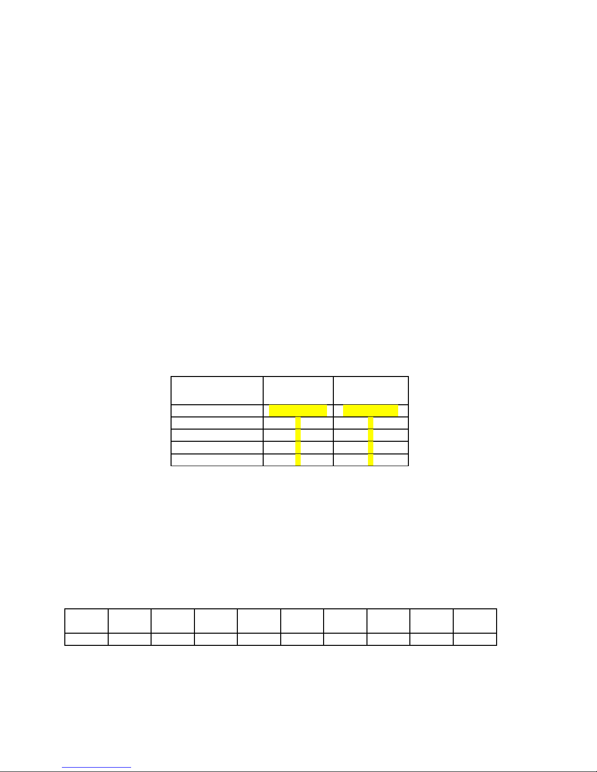
Baud Rate
Sw1/Switch 2 Sw1/Switch3
1200 0 0
9600 0 1
19200 1 0
57600 default 1 1
Table 7-1 Baud Rate Switch Settings
The RX-400A is set up with a fixed data word frame format consisting of ten bits, and
comprised of the following:
• one start bit,
• an eight-bit character
• no parity,
• one stop bit
An example illustration of the fixed data word format is shown below.
Start
Bit
Bit 0 Bit 1 Bit 2 Bit 3 Bit 4 Bit 5 Bit 6 Bit 7 Stop
Bit
PN 74446
7-1
Page 33

It is important in serial data transmissions that the receiving device knows when data is
being transferred and when data being transferred is about to stop. This information is
conveyed by the above start and stop bits. The start bit synchronizes the receiving
device so it reads the data properly. The stop bit notifies the receiving device that the
data frame has ended. The RX-400A’s fixed data word frame format does not contain a
parity bit.
7.2.1 Communications Protocols
Data transfers are handled via input and output buffers. The input buffer is handled in
circular fashion allowing simultaneous inputting and processing of data. The input
buffer accepts up to 256 bytes before overflowing. As data in the buffer is being
processed, up to 16 additional characters can be accepted by the unit. Upon receiving
a terminator character, the RX-400A processes any previous messages in the buffer.
The input buffer processing starts on the receipt of a terminator (CR). If the
communications error flag is set, the buffer contents from the end of the last processed
message thru the message terminator are discarded. In the event the buffer is
overrun, its contents are discarded. All other incoming data is buffered and processed
in the order in which it was received. If the radio does not understand a command
sequence or the command is badly formatted, the radio will respond with a ‘Z’ followed
by a carriage return.
The output buffer is handled in circular fashion allowing simultaneous additions and
outputting.
7.3 COMMAND MESSAGE FORMATTING
Command messages for the RX-400A are exclusively ASCII-encoded data, consisting of
command headers and arguments. Command headers consist of a two character
(letter-digit) mnemonics. All queries consist of a question mark (?) followed by a
command header. All set commands consist of an asterisk (*) followed by a command
header.
7.4 TERMINATORS FOR COMMANDS AND QUERIES
Terminators are used to signal the end of a command or string. When a properly
formatted message is ready to be sent, a CR (carriage return) character should be
entered. The CR character instructs the receiver to process the preceding messages.
The RX-400A also transmits a terminator when responding to queries. After the query
response is transmitted the receiver issues a CR (carriage return) indicating the end of
the response.
7-2
PN 74446
Page 34
7.5 FORMATS OF QUERY RESPONSES
The RX-400A transmits responses to queries in a fixed-field format. Query responses
begin with the letter-digit mnemonic of the query in upper-case characters, followed by
an alphanumeric argument. Numeric arguments are represented by the least number
of digits possible, while still representing the entire range of the value. If a negative
value is allowed for the argument, a positive or negative sign is always given. Multiple
responses to a query are valid but are separated by a CR character.
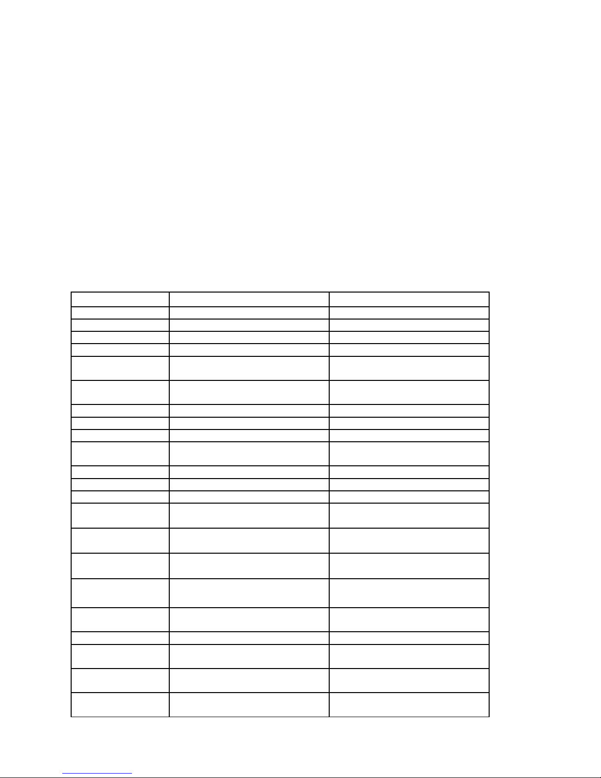
7.6 CONTROL PARAMETERS
Various receiver parameters can be controlled and /or monitored over the USB or
Ethernet interface. See Table 7-2 below for supported control commands. Note: All
commands are 2 ASCII characters.
TABLE 7-2 COMMAND PARAMETERS
Description Set Command Query Command
Set Attenuator *A0 ?A0
BITE Level 1 *B1 Not Applicable
BITE Level 2 *B2 Not Applicable
BITE level 3 *B3 Not Applicable
Store Memory
Channel
Set Manual
Attenuation
BFO *C2 ?C2
Bandwidth *C3 ?C3
Store Sweep Range *C4 ?C4
Automatic Gain
Control
Detection Mode *C7 ?C7
Memory Recall *C8 Not Applicable
Software Reset *C9 Not Applicable
Load EEprom
Defaults
Reset AGC Settings *D2 Not Applicable
*C0 Not Applicable
*C1 ?C1
*C5 ?C5
*D1 Not Applicable
Stop Ethernet Audio
RIP
Start Ethernet
Audio RIP
Set Ethernet IP
Address
Set Base UDP Port *E3 ?E3
Set Gateway Router
IP Address
Disable Ethernet
Communications
Enable Ethernet
Communications
*E0 Not Applicable
*E1 Not Applicable
*E2 ?E2
*E4 ?E4
*E5 Not Applicable
*E6 Not Applicable
7-3
Page 35
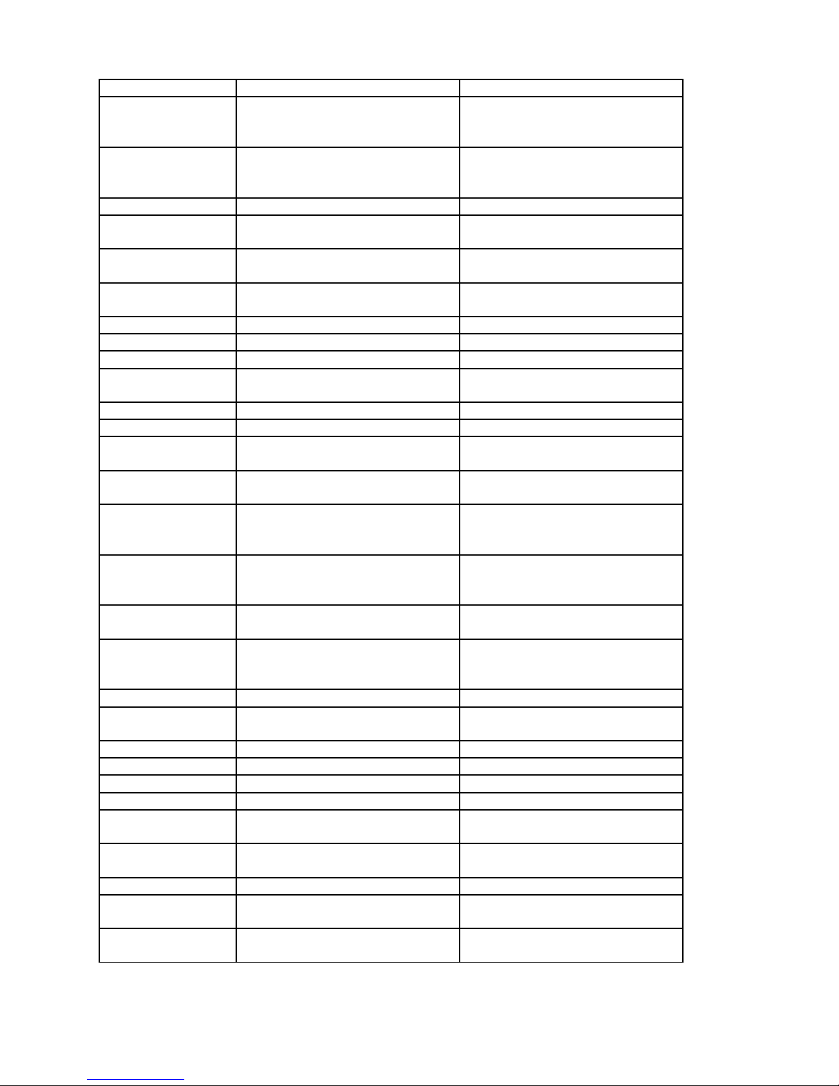
Table 7-2, Continued
Tune Frequency *F1 ?F1
Start /End
Frequency Range
for Frequency Scan
Start/Halt/Pause/Re
sume Frequency
Scan
Frequency Step *F5 ?F5
Add/Delete Lockout
Frequency
Add/Delete Lockout
Frequency Range
Add Lockout
Frequency Range
Set Attack Rate *G1 ?G1
Set Decay Rate *G2 ?G2
Set Hang Time *G3 ?G3
Unit Serial
Number
Firmware Version Not Applicable ?I2
Fault Status Not Applicable ?I3
Extended Firmware
Info
Recall Memory
Channel
Store current
parameters in
Memory Channel
Memory Scan
Channel Range
Start/Stop
Memory Scan
Channel Skip/Add
Memory-Scan
Channel
Halt/Pause/Resume
Set Squelch Level *S1 ?S1
Report Signal
Strength
Squelch Status Not Applicable ?S4
Dwell Timer *T1 ?T1
Dead Time *T2 ?T2
Gaze Time *T3 ?T3
S-Meter Hold off
Time
Set Carrier Loss
Time
Set Transient Time *T6 ?T6
Disable Multi
Address mode
Enable Multi
Address Mode
*F2 ?F2
*F3 ?F3
*F6 ?F6
*F7 ?F7
*F8 ?F8
Not Applicable ?I1
Not Applicable ?I4
*P0 ?P0 (report only)
*P1 Not Applicable
*P2 ?P2
*P3 ?P3
*P4 Not Applicable
*S3 ?S3
*T4 ?T4
*T5 ?T5
*U1 ?U1
*U2 ?U2
7-4
Page 36
7.6.1 Command Descriptions
The following will define a functional description of each control command or query
command supported in the RX-400A Receiver.
Hardware HF Attenuator On/Off
Controls the hardware attenuator. This attenuator is active in the HF bands only.
Format : (Set command) *A0n<cr>
(Get command) ?A0<cr> Response: A0n<cr>
1)
Definitions:
BITE, System Self-Test (B1, B2, B3)
N= 1 or 0, where 1 turns the attenuator on and 0 turns the attenuator off.
Where 1= 20dB and 0= 0dB
BITE, System Self Test (B!,B2,B3)
Initiates the BITE process. When completed, the system will report PASS or FAIL.
Store Memory Channel (C0)
Format : (Set command) *Bn<cr>
1) The system will run internal diagnostics and report PASS or FAIL.
Definitions:
N= 1,2 or 3,
Store Memory Channel
Stores current operating Frequency and Detection Mode to the indicated memory channel
Format : (Set command) *C0nnn<cr>
Definitions:
1) n=3 digit memory channel 0 to 999.
7-5
Page 37

Set Manual AGC Attenuation
Sets the amount of AGC attenuation to apply. Adjusts from 000-120 dB range with 0.10 dB
resolution. Can be set in any mode. Receiver gain is reduced and AGC threshold is increased
by the number of dB indicated.
Format : (Set command) *C1AAAD<cr>
(Get command) ?C1<cr> Response: C1AAAD<cr>
1)
Definitions:
AAA= 000-120 represents the amount of attenuation in db. Range 000-120
D=represents .10 resolution for the attenuation. Example: 107.8 dB attenuation will
be entered as 1078. Decimal point is not allowed.
BFO (C2)
Format: (Set command) *C2nnnn<cr>
(Get command) ?C2nnnn<cr>
Definitions:
For CW detection mode operations, The Beat Frequency Oscillator (BFO) capability is available. The
BFO is adjustable over a +/- 8192 Hz range in 1Hz steps. The BFO frequency can be applied to the
received CW signal to alter its audio pitch as a detection aid. The BFO frequencies are selected by the
BFO commands.
7-6
Page 38
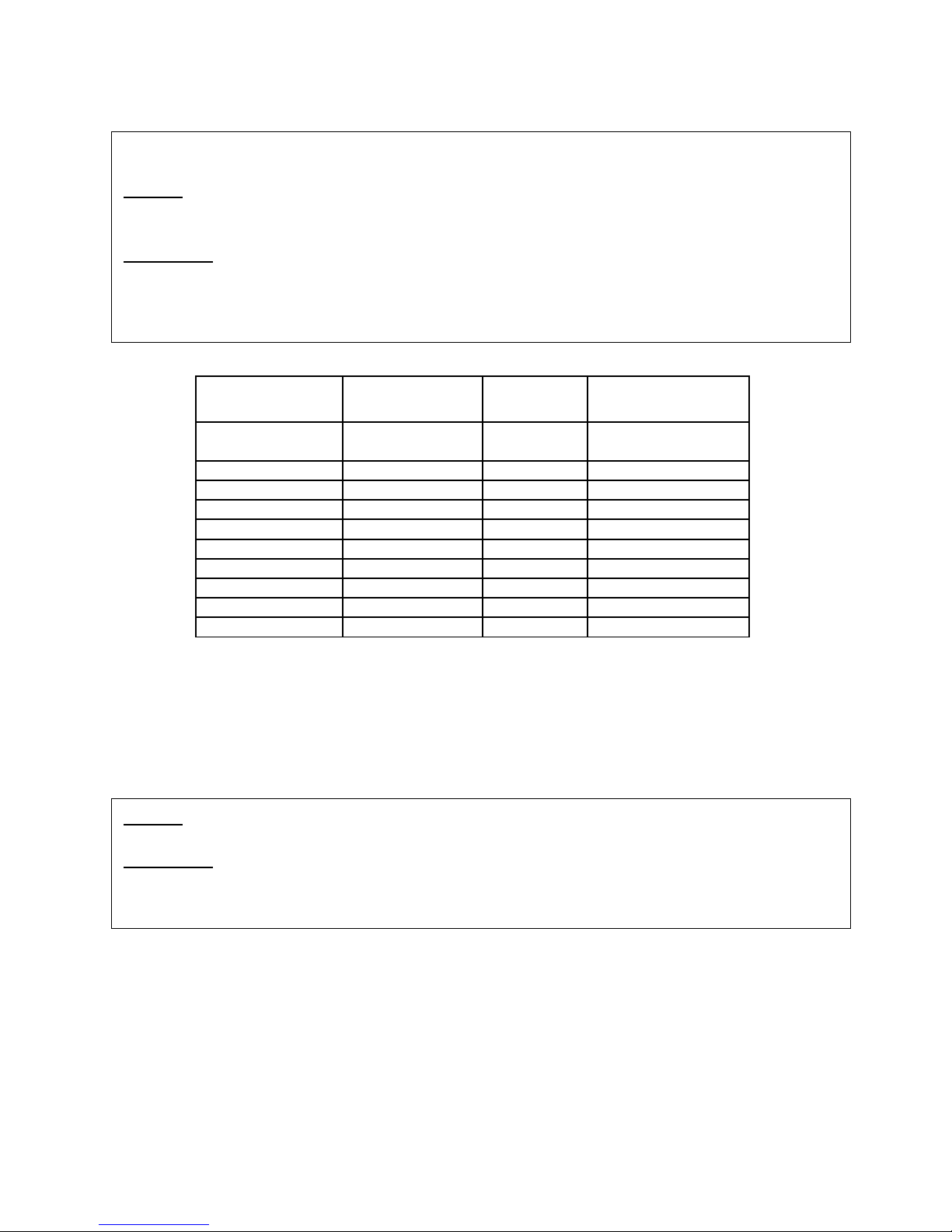
Bandwidth (C3)
The operator may select one of 18 available IF bandwidth filters.
Format: (Set command) *C3BB<cr>
(Get command) ?C3<cr> Response: C3BB<cr>
Definitions:
BB selects the desired bandwidth using 2 ASCII decimal digits. See Table 7-3 for Filter
selections. Note: Filter numbers are 2 ASCII digits. Example <0><0> for filter number 0.
Filter Number Bandwidth Filter
Number
00 300khz 10 20khz
01 240khz 11 15khz
02 180khz 12 10khz
03 150khz 13 6khz
04 100khz 14 5khz
05 60khz 15 3khz
06 50khz 16 2khz
07 35khz 17 1khz
08 30khz 18-27 900-100hz
09 25khz
Table 7-1 Bandwidth Filters
Store Current Parameters in Sweep Range A-H (C4)
Format: (Set command) * C4<cr>
(Get command) ?C4<cr>
Definitions:
Automatic Gain Control (C5)
Bandwidth
7-7
Page 39
Automatic Gain Control (C5)
The receiver provides 3 preset Automatic Gain Control rates and a programmable AGC mode. The
operator may select Slow, Medium, Fast or Programmable via the C5 command. The three modes are
selected as defined:
Format: (Set command) *C5X<cr>
(Get command) ?C5<cr> Response: C5X<cr>
Definitions:
X =<S>-- select SLOW mode <M>--selects MEDIUM mode <F>--selects FAST mode
<P>--Programmable Mode
Default--<M> MEDIUM setting
If programmable mode is selected, the radio will use the value entered via the G1, G2 and G3 (Set
Attack, Decay and Hang Rate) command.
Detection Mode (C7)
Format: (Set Command) *C7M<cr>
(Get Command) ?C7<cr>
Definitions:
M=<A>=AM, <U>=USB, <L>=LSB, <C>=CWU, <W>=CWL, <F>=FM, <K>=FSK
The detection mode command determines how the signal is to be demodulated. The Receiver
Supports AM, USB, LSB, CWU, CWL, FM and FSK detection modes.
Memory Recall ( C8)
Format: (Set command) * C8nnn<cr>
(Get command) ?C8nnn<cr> Where nnn is value between 0 and 999
Definitions: Command used to recall memory channel contents. If memory empty, then no
action is taken.
Format: (Set command) *C7M<cr>
(Get command) ?C7<cr> Response: C7M<cr>
7-8
Definitions:
M= <A>=AM, <U>=USB, <L>=LSB, <C>=CWU, <F>=FM , <W>=CWL, <K>-= FSK
The detection mode command determines how the signal is to be demodulated. The receiver
supports AM, USB, LSB, CWU, FM, CWL, FSK detection modes. The detection mode will be
selected for the current frequency selected by the receiver. AUTO MODE??
Page 40
Software Reset (Reboot) Unit (C9)
Format: (Set command) *C9<cr>
(Get command) (Not applicable)
Definitions:
This command will perform a soft reboot to the receiver. The unit will be initialized as if the
power were removed. The ASCII string “RADIO START” will be transmitted by the radio
when reset is complete.
Software Reset (Reboot) Unit (C9)
Load EEprom Defaults (D1)
Format: (Set command) *D1PPPPP<cr>
(Get command) (Not applicable)
Definitions:
PPPPP is the 5 ASCII digit pass code that must be entered to download default values to EEprom and is
defined as:
AGC DUMP (D2)
12461
This command will load all defaults settings to EEPROM. A valid five character password
must enter with this command before the command will be accepted.
NOTE: This command could take up to 10 seconds to complete. The user should wait for the
ASCII string “RADIO START” that will be transmitted by the radio when the download is
complete.
AGC Dump (D2)
Format: (Set command) *D2<cr>
(Get command) (Not applicable)
Definitions:
This command will terminate the current AGC state and refresh the AGC system. This will
cancel HANG or DECAY in process. This is most effective for canceling a long AGC recovery
delay that may be suppressing the receiver gain and reducing sensitivity.
7-9
Page 41
Stop Ethernet Audio Rip (E0)
This command stops the transmission of RIP (Radio over IP) audio via Ethernet UDP protocol.
Format: (Set command) * E0<cr>
(Get command) (Not applicable)
Definitions:
Start Ethernet Audio Rip (E1)
Start Ethernet Audio Rip (E1)
This command starts the transmission of RIP audio ethernet packets. This command must be
sent out a minimum of every 5 seconds for the unit to continue to send rip packets via ethernet.
Format: (Set command) * E1<cr>
(Get command) (Not applicable)
Definitions:
Set Ethernet IP Address (E2)
Format: (Set command) *E2AAA<dot>BBB<dot>CCC<dot>DDD<cr>
Set Gateway Router IP address (E4)
(Get command) ?E2<cr>
Response: E2AAA<dot>BBB<dot>CCC<dot>DDD<cr>
Definitions:
AAA—The 1st octet of the IP address. Range 0-255
BBB—The 2nd octet of the IP address Range 0-255
CCC—The 3rd octet of the IP address Range 0-255
DDD—The 4th octet of the IP address Range 0-255
Disable Ethernet Communications Port (E5)
The octet addresses can be specified using 1, 2, or 3 digits. If less than 3 digits are specified
for the octet address, a “dot” character<0x2E> must sent between the octets to differentiate
between address values.
7-10
Page 42
Set Base UDP Port (E3)
Format: (Set command) * E3NNNNN<cr>
(Get command) ?E3<cr> Response: E3NNNNN<cr>
Definitions:
This command will set the 5 digit UDP port value for the radio.
NNNNN- valid range 0-65520.
Set Gateway Router IP Adress (E4)
Format: (Set command) * E4AAA<dot>BBB<dot>CCC<dot>DDD<cr>
(Get command) ?E4<cr>
Response: E4AAA<dot>BBB<dot>CCC<dot>DDD<cr>
Definitions:
AAA—The 1st octet of the gateway IP address. Range 0-255
BBB—The 2nd octet of the gateway IP address Range 0-255
CCC—The 3rd octet of the gateway IP address Range 0-255
DDD—The 4th octet of the gateway IP address Range 0-255
The octet addresses can be specified using 1, 2, or 3 digits. If less than 3 digits are specified
Enable Ethernet Communications Port (E6)
for the octet address, a “dot” character<0x2E> must sent between the octets to differentiate
between address values.
Disable Ethernet Communications Port (E5)
Format : (Set command) *E5<cr>
(Get command) (Not applicable)
Definitions:
This command will disable Ethernet communications.
7-11
Page 43
Enable Ethernet Communications Port (E6)
To tune a value of 2 MHz 2000000 can be entered.
Format: (Set command) *E6<cr>
(Get command) (Not applicable)
Tune Frequency ( F1)
Definitions:
This command will enable Ethernet communications.
Tune Frequency (F1)
.
The F1 command allows the tuned frequency of the RX-400A to be set to any value between
100kHz and 3 Gigahertz in 1-Hz increments.
Format : (Set command) * F1FFFFFFFFFF<cr>
(Get command) ?F1<cr> Response:
F1FFFFFFFFFF<cr>
Definitions:
FFFFFFFFFF-Selects the frequency to tune in hertz entered as10 ASCII/decimal format. Leading zeros can
be omitted. Range 2 MHz to 3 GHz
Example:
To tune a frequency of 235.67 MHz the value 235670000 will be entered.
Start/End Frequency (F2)
This command is used to select the start and end frequency range for P-SCAN mode which
allows the radio to search for activity in a given frequency range.
Format: (Set command) * F2SSSSSSSSSS<dot>EEEEEEEEEE<cr>
(Get command) ?F2<cr>
Response: F2SSSSSSSSSS<dot>EEEEEEEEEE<cr>
Definitions:
SSSSSSSSSS --Selects the starting frequency in hertz. The value entered in 10 ASCII
/decimal format. Leading zeros can be omitted but the <dot> character must be transmitted to
differentiate between the start and end frequency values. Range 100kHz-3 GHz
EEEEEEEEEE-- Selects the ending frequency in hertz. The value entered in 10 ASCII
/decimal format. Leading zeros can be omitted. Range 100kHz-3 GHz
7-12
Page 44
Start/Halt/Pause/Resume Frequency Scan ( F3)
Format: (Set command) * F3X<cr>
(Get command) ?F3<cr> Response: F3X<cr>
Definitions:
X = <S> start programming frequencies for the specified range using command F2. If no range has been
specified using command F2, the receiver, the valid range will be from 0-3Ghz in 1hz increments if no step
size is specified via command F5. If command F5 has been received, the receiver will use the step size
specified in that command.
<H> halts or stops frequency scanning and returns to manual mode. The receiver will remain
tuned to frequency it is currently set to when receiving this command.
<P> Scanning will pause scanning if currently in scan mode. This command is ignored if not
currently in scan mode.
<R> resumes frequency scanning if currently in “paused” mode. Ignores this command if not
`
currently in paused mode
Frequency Step (F5)
Add Lockout Frequency (F6)
Frequency Step (F5)
Sets the step size of frequency scan (1 Hz steps) in P-SCAN mode
Format: (Set command) *F5FFFFFFFFFF<cr>
(Get command) ?F5<cr> Response:
F5FFFFFFFFFF<cr>
Definitions:
Delete Lockout Frequency (F7)
FFFFFFFFFF-Selects the step size in hertz entered in ASCII/decimal format. Leading zero’s
can be omitted. Range 1 Hz-3 GHz
7-13
Page 45
Add Lockout Frequency (F6)
BBBBBB=specifies the 6 digit ASCII/decimal bandwidth to add/subtract from the specified
EEEEEEEEEE- Specifies the ending frequency for the lockout range entered in ASCII/decimal format.
Format: (Set command) *F6NNFFFFFFFFFF<dot>BBBBBB<cr>
(Get command) ?F6NN<cr>
Response: F6NNFFFFFFFFFF<dot>BBBBBB<cr>
Definitions:
NN= Specifies the record number where the lockout frequency is stored. Valid record numbers
0-49.
Note: If NN value is 00 the radio will respond with all the record numbers and values that are
programmed in the following format:
Set Attack Rate (G1)
F6NNFFFFFFFFFF<dot>BBBBBB<cr>
F6NNFFFFFFFFFF<dot>BBBBBB<cr>
F6NNFFFFFFFFFF<dot>BBBBBB<cr> …..etc.
:
FFFFFFFFFF=specifies the 10 digit ASCII/decimal frequency value to lock out when tuning.
Leading zeros can be omitted but the <dot> character must be transmitted to differentiate
between the frequency and the bandwidth values.
Delete Lockout Frequency (F7)
Format: (Set command) *F7NN<cr>
(Get command) (Not applicable)
Definitions:
NN= Specifies the record number in which to delete the lockout frequency value that is stored
Add Lockout Frequency Range (F8)
Format: (Set command) *F8NNSSSSSSSSSS<dot>EEEEEEEEEE<cr>
1) (Get command) ?F8NN<cr>
1) Response:
F8NNSSSSSSSSSS<dot>EEEEEEEEEE<cr>
Definitions:
NN—specifies the record number 0-24
Note: If NN value is 00 the radio will respond with all the record numbers and values that are
programmed in the following format:
*F8NNSSSSSSSSSS<dot>EEEEEEEEEE<cr>
*F8NNSSSSSSSSSS<dot>EEEEEEEEEE<cr>
1) *F8NNSSSSSSSSSS<dot>EEEEEEEEEE<cr>
SSSSSSSSSS- Specifies the starting frequency for the lockout range entered in ASCII/decimal
format. . Leading zeros can be omitted but the <dot> character must be transmitted to
differentiate between the leading frequency and the ending frequency values.
Range 0-3Ghz
7-14
Page 46
Set Attack Rate (G1)
Format: (Set command) *G1NNNN<cr>
(Get command) ?G1<cr>
Response: G1NNNN<cr>
Definitions:
NNNN=Valid range 0001-9999 in ASCII decimal format. Leading zeros can be omitted.
The attack rate is used in automatic gain control (AGC) to select the rate to raise the volume for weak signals to try to maintain
an approximately constant average output level of varying signal levels.
Set Hang Time (G3
)
Unit Fault/Error Status (I1)
Set Decay Rate (G2)
Format: (Set command) *G2NNNN<cr>
(Get command) ?G2<cr> Response:
G2NNNN<cr>
NNNN=Valid range 0001-9999 in ASCII decimal format. Leading zeros can be omitted.
Firmware Version (I2)
The attack rate is used in automatic gain control (AGC) to select the rate to lower the volume for strong signals to try to
maintain an approximately constant average output level of varying signal levels.
Set Hang Time (G3)
Format: (Set command) *G3NNNN<cr>
(Get command) ?G3<cr> Response: G3NNNN<cr>
NNNN=Valid range 0001-9999 in ASCII decimal format. Leading zeros can be omitted.
7-15
Page 47
Unit fault Status (I1)
Format: (Set command) *I1KKKKKKKKKK<cr>
( Get Command) ?I1<cr>
Response: By single character letter code
KKKKKKKKKK – This will be a key code used in the set command to clear out all error
codes logged in the unit. The key code will be a 10 character hard coded value used by TenTec Service to clear out the error codes.
Error Code Definitions:
This command will report error codes and fault conditions via one alphabetic character that are
logged by the firmware. They are defined as follows:
A=
B=
C=
D=
Firmware Version (I2)
Format: (Set Command) Not Applicable
(Get Command) ?I2<cr> Response: CCCCCCCCCCCCC<cr>
Definitions:
This command will report the firmware version number. The following strings are defined
and will be reported for the specific unit model numbers.
RX-400A Model:
VER<0x20>XXXX<0x5f>400<cr> Note: XXXX represents 4 digits that will increment
with each Firmware version release.
Format: (Set command) (Not applicable)
(Get command) ?I2<cr> Response:
CCCCCCCCCCCCC<cr>
Definitions:
This command will report the firmware version number. The following strings are defined and
will be reported for the specific unit model numbers:
RX400 model:
VER< 0x20>XXXX< 0x5f>400<cr> Note: XXXX represent 4 digits that will increment with each
Firmware version release.
7-16
Page 48
Unit Serial Number (I3)
Format: (Set command) (Not applicable)
(Get command) ?I3<cr> Response:
I3SSSSSSSS<cr>
Definitions:
This command will report the serial number assigned to each unit by Ten-Tec. The following
format is defined:
To be determined
Extended Firmware Info (I4)
Format: (Set command) (Not applicable)
(Get command) ?I4<cr> Response: to be determined
Store To Memory Channel (P0)
Stores current operating Frequency and Detection Mode to the indicated memory channel
Format : (Set command) *P0nnn<cr>
(Get command) ?P0nnn<cr> reports contents of memory channel without
recalling the data.
Definitions:
1) n=3 digit memory channel 0 to 999.
7-17
Page 49
Store Current Parameters in Memory Channel (P1)
Format: (Set command) *P1CCCBBMSSRFFFFFFFFFF<cr>
1) (Get command) ?P1CCC<cr> Response:
P1CCCBBMSSRFFFFFFFFFF<cr>
Definitions:
CC=Channel Number to assign parameters. Range 00-999 in ASCII/decimal format
BB=Selected IF Bandwidth filter number assigned to the specified channel number. Range: (See Table 5)
M=Selected detection mode assigned to the specified channel <A>=AM, <F>=FM, <U>=USB,
<L>=LSB,
<C>=CWU, <W>=CWL, <K>=FSK
SS=Selects the desired squelch mode settings. Multiple squelch modes can be selected.
R=<A>=channel specified in command is added to the channel ring.
=<D>=channel specified in command is deleted from the channel ring.
FFFFFFFFFF=Frequency to tune assigned to specified channel number. Range 100kHz-3
GHz Leading zero’s can be omitted.
Memory-Scan Channel Start-Stop Range (P2)
Format: (Set command) *P2SSSEE<cr>
1) (Get command) ?P2<cr> Response:
P2SSSEE<cr>
Definitions:
SS= Specifies the starting channel for the memory scan via two ASCII digits. Range 0-999.
EE= Specifies the ending channel for the memory scan via two ASCII digits. Range 0-999.
Memory Channel Skip/Add (P3)
Format: (Set command) *P3CCCX<cr>
1) (Get command) ?P3CCC<cr> Response:
P3CCCX<cr>
Definitions:
CC=specifies the channel to be added or deleted to the memory list when scanning. Range 0999
X= <A> adds the specified channel to the memory list when scanning.
= <S> removes the specified channel from the memory list when scanning.
7-18
Page 50

Start/Halt Pause/Resume Memory Scan (P4)
Format: (Set command) *P4X<cr>
(Get command) (Not applicable)
Definitions:
X = <S> start scanning for activity on pre-programmed memory channels. The receiver will use the specified
channel range via command P4. If no range has been specified using command P4, the valid channel range
will be from 0-999.
NOTE: if no channels are found to be programmed, an error will be returned when the “S” is
transmitted to start scanning.
NOTE: the time between scanning uses the time set in the Gaze Time (T3) command.
<H> halts or stops program scanning and returns to manual mode. The receiver will remain tuned to
the channel it is currently set to when receiving this command.
<P> pauses channel scanning if currently in scan mode. Ignored if receiver not currently in scan
mode.
<R> resumes channel scanning if currently in “paused” mode. Ignores this command if not currently
in paused mode
Squelch Notes:
Unlike HF receivers, VHF/UHF receivers need noise squelch, window squelch and signal
level squelch. It is not sufficient to rely on carrier to noise ratio alone to determine if
signal is present in a channel.
Set Signal Strength Squelch (S1)
Format: (Set command) *S1LLL<cr>
(Get command) ?S1<cr> Response: S1LLL<cr>
Definitions:
LLL—the level that will be compared to the current signal strength level used to determine if a
valid signal is present. If the current signal strength is found to be less than this value, the
signal is found to be invalid and the audio will be muted. Valid ranges 0-127. Leading zero’s
can be omitted.
7-19
Page 51
Current Signal Strength (S3)
Format: (Set command) (Not applicable)
(Get command) ?S3<cr>
Response: S3NNN<cr>
NNN= Current measurement of signal strength. Valid ranges 0-127
This command will report the current signal strength value that is updated in the firmware. This is the value
that is compared to the squelch level set in the S1 command. If this value goes below the squelch level, the
audio will be muted.
Squelch Status (S4)
Squelch Status (S4)
Format: (Set Command) (Not applicable)
(Get command) ?S4<cr>
Definitions: TBD
Dwell Timer (T1)
Format: (Set command) *T1TTTTTTTT<cr>
(Get command) ?T1<cr> Response: T1TTTTTTTT<cr>
1)
Definitions:
TTTTTTTT= represents the time in ASCII/decimal format. Value = number of
milliseconds. Valid ranges are 0-99999999.
The dwell time feature sets the duration of time the receiver will remain on an active channel.
An infinite dwell time can also be selected. Setting the Dwell Time to 0 activates the
INFINATE DWELL which forces the radio to remain on the frequency or memory channel as
long as it is active (SQUELCH open).
7-20
Page 52

Dead Time (T2)
Format: (Set command) *T2TTTTTTTT<cr>
(Get command) ?T2<cr> Response:
T2TTTTTTTT<cr>
TTTTTTTT= represents the time in ASCII/decimal format. Value = number of milliseconds.
Valid ranges are 0-99999999.
Dead time refers to the time the radio will remain on a channel after activity has ended. The
factory default is 8 seconds. If the DWELL TIME setting is less than the DEAD TIME setting
the radio will resume scanning when the DWELL TIME timer runs out. If the DWELL TIME
setting exceeds the DEAD TIME setting, scanning will resume when the DEAD TIME timer
runs out.
Gaze Time (T3)
Format: (Set command) *T3TTTTTTTT<cr>
(Get command) ?T3<cr> Response: T3TTTTTTTT<cr>
TTTTTTTT= represents the time in ASCII/decimal format. Value = number of milliseconds.
Valid ranges are 0-99999999.
Gaze time is the time the radio will spend waiting for activity on each new channel or
frequency. The factory setting is 50Ms. This time can be adjusted to control the rate of scan.
S-Meter Hold Off Time (T4)
Format: (Set command) *T4TTTTTTTT<cr>
(Get command) ?T4<cr> Response:
T4TTTTTTTT<cr>
TTTTTTTT= represents the time in ASCII/decimal format. Value = number of milliseconds.
Valid ranges are 0-99999999.
This feature determines how long the radio will wait before checking channel activity after moving to
a new frequency or channel. This time is necessary to allow the AGC system to settle down so an
accurate measure of channel activity can be made. Factory defaults to 50ms.
7-21
Page 53

Disable Multi-Addressing Switch Override (U1)
This command disables the Multi addressing override mode. The firmware will set/clear multi
addressing mode via Dip Switch SW1, switches 4-8. If all the switches are set to the ON
position, multi addressing is disabled and the unit will respond to all commands. If the dip
switches are set to any other position, multi address mode is enabled and the unit will respond
only to commands that have the binary address selected via the dip switches of the unit. Switch
4 = MSB, Switch 8 = LSB.
Format: (Set command) *U1<cr>
(Get command) (Not applicable)
Description:
Enable Multi-Addressing Switch Override (U2)
Format: (Set command) *U2<cr>
(Get command) (Not applicable)
Description:
When this command is received, the multi addressing mode is ignored and all the units
connected on the serial or Ethernet bus assumes non multi addressing mode. The units will
respond to all commands until they have been reset via the C9 command, power reset, or the
U1 command.
Mission Download (M0)
Format: (Set command) *M0<cr>
(Get command) (Not applicable)
Description:
Command set passed from system host/workstation through RCU-400A to RX-400A to set
fstart, fstop, fstep, filterBW, detection mode, rfgain, squelch, AGC mode, attack, decay, hang,
gaze, dwell, deadtime, memory channel group<cr. Where CC=Mission Memory Channel
and MT=Memory Type is ( R) range or ( C) channel. Example: *M01,02,R,0088000000,
0108000000,0000100000,10,F,0,040,F,99,88,77,10,50,90,21
7-22
Page 54

8.0 AUDIO STREAMING
8.1 RADIO OVER IP (RIP) DATA FORMAT
RIP is the system by which the RX-400A provides real time streaming audio. The RIP
packets are sent from the radio via standard UDP packets. With each UDP packet
containing a descriptive header and audio data block. The RIP UDP Packet is based on
the Real Time Protocol (RTP). RTP is the format utilized by various commercial Voice
Over IP systems. The format of the data packet used for RIP is as follows:
Octet 0 Header Information 0x80 = RTP Format
Octet 1 Header Information Continued 0x50
Octet 2-3 RTP Sequence 0xnn 0xnn
Packet Counter (=last+1) used for verification of service
Octet 4-7 RTP TimeStamp 0xnn 0xnn 0xnn 0xnn
Time Counter (=last+64)
Octet 8-11 RTP Sync Source 0x45 0xmm 0xnn 0xoo
ID of the Radio (last 4 MAC digits)
The above octets were arranged so that a third party program that supports RTP audio
protocol could already use the packets from the RX-400A.
Additional header information is included that is specific to the RX-400A.
Octet 12-15 Sampling Frequency 0x00 0xmm 0xnn 0xoo
MSB first. e.g. if sampling frequency is 54081
the value returned would be 0x00 0x00 0xd3 0x41.
Because the RX400 sample rate is related to filter
selection this will change when filters are changed.
128 octets Audio Data 0xnn…
The audio data samples are two octets long and there are 64 of
them.
Format is 2 octets per sample MSB first.
There are two commands to start and stop the RIP process.
Stop Ethernet RIPing *E0<cr>
Start Ethernet RIPing *E1<cr>
9.0 MAINTENANCE
PN 74446
8-1
Page 55
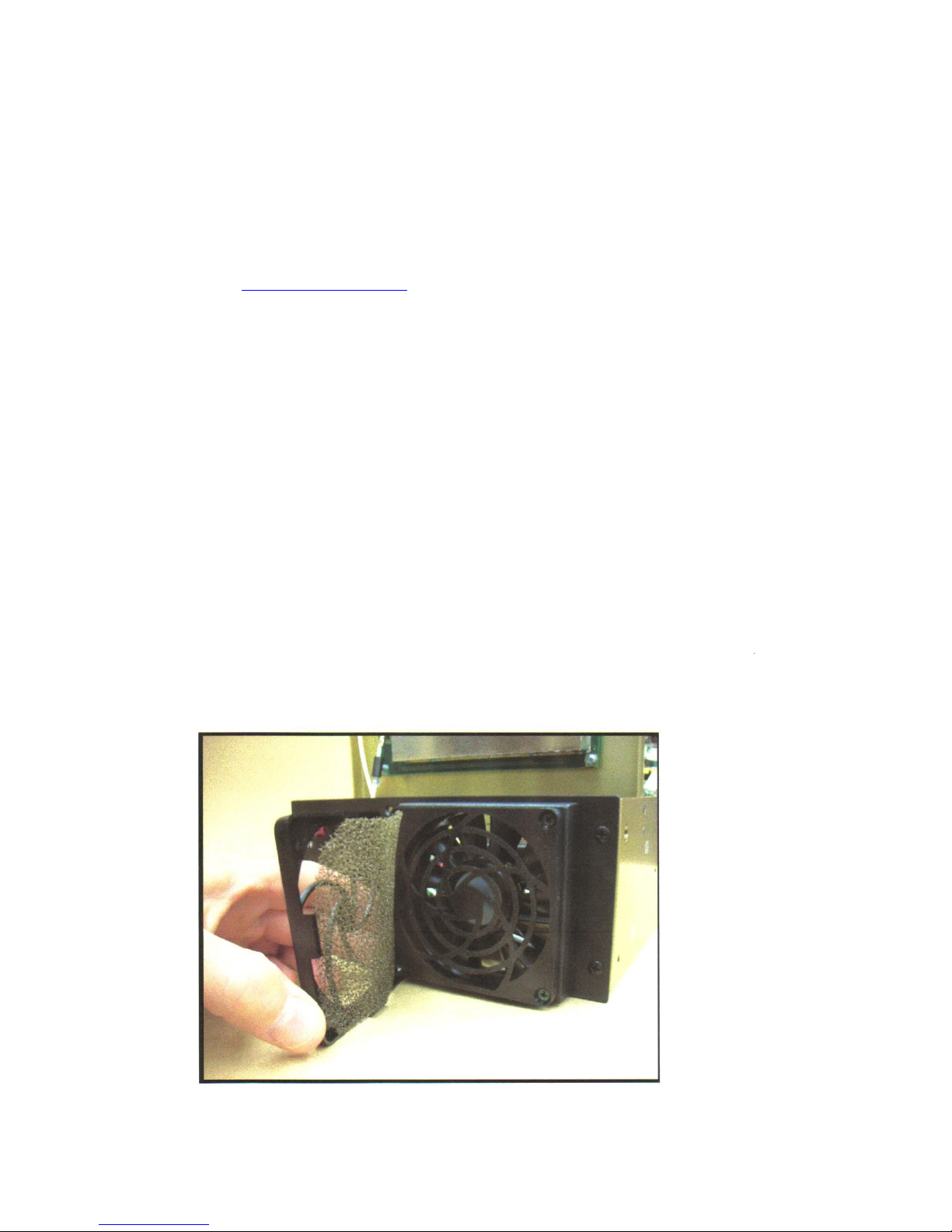
9.1 FACTORY SERVICE
The RX-400A Receiver is designed to provide reliable service, however, should nonrecoverable faults or equipment failure occur it is recommended the unit be returned to
TEN-TEC, Inc. for repair. The TEN-TEC Service Department provides quick turn-around
for most repairs. RMA numbers are not required. You may contact TEN-TEC to arrange
for service at: (865) 428-0364. Hours are 8:00AM-5:00PM, Monday through Friday. Or
send e-mail to: [email protected]
If known please indicate the nature of the fault or defect. Also include return shipping
address and any special instructions related to marking or packing.
9.2 CLEANING AND LUBRICATION
Panel surfaces may be cleaned using a soft damp cloth and a mild detergent solution.
Never use caustic cleaners or any type of solvent as this may damage painted and
chem-treated surfaces and plastic parts and knobs.
The Receiver cooling fan filter will require periodic cleaning or replacement dependent
on the operating environment. The filter can be removed and replaced by grasping the
edges of the fan bezel and pulling straight back. Wash the filter in a mild detergent
solution, then let air dry. Wipe the fan housing with a damp soft cloth.
solvents of any kind as this may damage or dissolve the filter element.
Never use
Replace the
filter element into the fan housing and snap on the fan bezel (see Figure 9-1).
9.3 INSPECTION
FIGURE 9-1 FAN ELEMENT REMOVAL
PN 74446
9-1
Page 56

The RX-400A Receiver should be checked for external damage or component wear
periodically. This should include inspection of the front panel phone jacks for
looseness, proper power switch operation with illuminated red indicator with power ON,
volume control knob tight on it’s shaft and intact cooling fan bezel and filter element.
Any time the unit is out of the rack console or if access is available to the rear of the
Receiver, the rear panel connectors should be checked for damage or looseness.
9.4 PERFORMANCE VERIFICATION AND FAULT ISOLATION
User level maintenance is limited to those tests that can be made at the operator
position. Performance verification consists of normal operation of the unit, that is, the
receiver seems to exhibit adequate signal sensitivity through out the unit’s frequency
tuning range, detection mode selections match the signal demodulation, IF bandwidth
selections result in expected audio response results without distortion and that audio
outputs are present. It is also useful to check for proper operation of manual tuning,
F1-F2 scan mode and memory channel scan mode along with RF gain, squelch and BFO
function. Since the RX-400A is a ‘blank panel, no manual controls unit’, it is anticipated
these checks will be made using the companion RCU-400A Receiver Control Unit.
Fault isolation is also accomplished using the RCU-400A Receiver Control Unit. This is
done by depressing the RCU Menu Key and scrolling through to the RX BITE screen.
The BITE routine checks the RF-to-IF-to-Audio paths as well as communication between
the RX and RCU. The indication is either PASS or FAIL. Instructions are provided in the
RCU-400A User Manual.
9.5 FAN SPEED
The fan speed may be changed by the end user. The factory default is ‘Fast’. To
change the fan speed to ‘Slow’ first disconnect the AC power cord, then remove the fan
bezel and filter element as in paragraph 9.2 above. Then remove the four (4) screws
securing the fan to the front panel and let the fan lay on bench surface by its leads.
Looking through the fan opening in the front panel there is a 3-pin connector plugged
into a 4-pin circuit board connector on the left-hand side. Note that connector is
plugged into the forward most 3 pins. With needle nose pliers gently lift up the
connector off the 3 forward pins and move backwards and pug onto the rear most set
of 3 pins. This is the ‘Slow’ speed fan position. Replace the fan by the 4 screws
previously removed, then put in the filter element and snap on the fan bezel. This
completes the steps required to change the fan speed.
9-2 74446
10.0 PREPARATION FOR SHIPMENT OR STORAGE
Page 57

10.1 STORAGE
If the RX-400A Receiver is not going to be used for an extended period of time (in
excess of 30 days) it should be stored in its sealed shipping carton or equivalent
container. The unit is rated for storage temperatures from –40 to +85 degrees C. To
prepare the unit for storage perform the following steps:
1. Remove all cords or cables attached to the unit.
2. Ensure there is sufficient bubble wrap or packing material in the container.
3. Place the unit in the center of the packing material.
4. Place packing material on top of the unit and seal the container.
5. Fasten labels or stamps and with indelible ink, write the word FRAGILE on all
sides of the container. Also write the model number, nomenclature, quantity and
serial number on the top of the container.
10.2 PREPARATION FOR SHIPMENT
If the RX-400A is required to be shipped to another location or back to the factory for
service, perform the steps in 10.1 above. Also include a packing slip, any pertinent
instructions or purchase order paperwork inside the container on top of the packing
material. Affix a shipping label to the outside of the container.
10-1
PN 74446
Page 58

This Page Intentionally Left Blank
PN 74446
 Loading...