

Page 1
74477
No. 1254
COMPLETE KIT WITH CASE,
HARDWARE
SSB-CW-AM
RECEIVER
Microprocessor-controlled,
15 Memories, dual conversion,
tunes 100 kHz to 30 MHz
KIT
by TEN-TEC
INSTRUCTION
MANUAL
America’s Best!
Page 2
Table of Contents
Section l: GETTING STARTED
A. General Introduction to Receiver Design and Features
B. About this Manual and T-KIT
C. Working with the Kit Parts Before Assembly
D. Detailed Kit Parts List
E. Checklist of supplies and tools needed for assembly
F. Component Identification Information
G. Building Electronic Kits: The Essent ials
H. Overview of Kit Assembly Phases
Section ll: Kit Assembly and Alignment
Detailed Table of Contents
Installing Parts on the Boards
Phase 1.0 Display Board Assembly
Notes on Main Board Assembly
Phase 2.0 Logic Section and Display Drivers
Phase 3.0 VCO's and PLL ("Phase-Locked Loop")
Phase 4.0 Receiver Audio, AM and Product Detectors,
455 kHz IF Amplifier, AGC system
Phase 5.0 2nd Mixer, 2nd LO, Clarifier control
Phase 6.0 RF Input, 1st Mixer, 1st LO amplifier
Phase 7.0 Final Assembly and Alignment
Section III: Reference Information
Detailed Table of Contents
Specifications: T-KIT Model 1254
Model 1254 Operating Instructions
Primary Controls
Circuit Description
Model 1254 Receiver Block Diagram
Practical Operating Information
GLOSSARY: Terms and Abbreviations
Component Reference Index
Troubleshooting Guide
including Chart of Significant Test Voltages
Checking for Solder Bridges
Page 3

Table of Contents
Primary Controls
Circuit Description
Model 1254 Receiver Block Diagram
Section l: GETTING STARTED
A. General Introduction to Receiver Design and Features
B. About this Manual and T-KIT
C. Working with the Kit Parts Before Assembly
D. Detailed Kit Parts List
E. Checklist of supplies and tools needed for assembly
F. Component Identification Information
G. Building Electronic Kits: The Essent ials
H. Overview of Kit Assembly Phases
Section ll: Kit Assembly and Alignment
Detailed Table of Contents
Installing Parts on the Boards
Phase 1.0 Display Board Assembly
Notes on Main Board Assembly
Phase 2.0 Logic Section and Display Drivers
Phase 3.0 VCO's and PLL ("Phase-Locked Loop")
Phase 4.0 Receiver Audio, AM and Produc t Detectors,
455 kHz IF Amplifier, AGC system
Phase 5.0 2nd Mixer, 2nd LO, Clarifier control
Phase 6.0 RF Input, 1st Mixer, 1st LO amplifier
Phase 7.0 Final Assembly and Alignment
4
5
6
8-13
14
15-17
18-19
20
1
2
3-10
11-12
14-24
26-35
36-46
48-55
56-63
64-72
Section III: Reference Information
Detailed Table of Contents
Specifications: T-KIT Model 1254
Model 1254 Operating Instructions
1 . Functions of
2. Storing Frequencies in Memory
3. Recalling or Tuning Memory Frequencies
4. Tuning AM signals
5. Tuning SSB signals
6. Tuning CW signals
7. Microprocessor RESET
8. Memory Battery Te st
Practical Operating Information
DC Power Supply, Audio, Antennas,
Special installations, SWL basics and more
GLOSSARY: Terms and Abbreviations
Component Reference Index
Troubleshooting Guide
including Chart of Significant Test Voltages
Checking for Solder Bridges
1254 - Getting Started – 2
1
2
3-5
6-14
8
15-23
24-28
25-35
36-39
40
Page 4

Table of Illustrations, Charts and Diagrams
ic details
Fig. 7.2: Functions of the chassis brackets
Fig. 1R: Frequency Display exam ple
Building one's own receiver from a kit has launched countless thousands
of people into communications careers or the hobbies of amateur radio
and shortwave listening ("SWLing"). The Model 1254 combines the
satisfaction of the kit-building experience with the performance features
expected in a modern shortwave receiver. You will build a true dual-
conversion superhet with precise microprocessor-controlled frequency
synthesizer. Alignment is surprisingly easy and does not require
complicated test equipment. Building this receiver yourself also gives you
the assurance that you can maintain it in perfect working order for years to
come.
General Features:
You will build the Model 1254 in seven sections or phases, testing your
work after completing each phase. We encourage you to study this entire
manual before beginning const ruction.
A. Introduction to Model 1254
Receiver Features and Design
1 . Getting Started Section
Selected Component Illust rations
16-18
2. Assembly Section
Phase 1.0 schemat
Phase 1.0 circuit board illustration
Fig. 1.1 : LED alignment
Fig. 1.2: Installation of J1 , J2
Fig. 1.3: Encoder wiring
Phase 2.0 schematic details
Phase 2.0 circuit board illustration
Fig. 2.1: Installation of P1, P2
Fig. 2.2: DC Power Input section
Phase 3.0 schematic details
Phase 3.0 circuit board illustration
Fig. 3.1: VCO-1 assembly
Fig. 3.2: VCO 2 assembly
Phase 4.0 schematic details
Phase 4.0 circuit board illustration
Fig. 4.1 : Headphone jack wiring
Phase 5.0 schematic details
Phase 5.0 circuit board illustration
Fig. 5.1: balun transformer details
Fig. 5.2: Installation of Q4, C63, Q7
Phase 6.0 schematic details
Fig. 6.1: RF Input Bandpass Filter Assembly
Fig. 6.2: First Mixer Assembly
Fig. 6.2b: Alignment Preview
Phase 6.0 Full circuit board illustration
Fig.7.1: Chassis and panel assembly overview
Table 7. 1: Small hardware preview
14
15
17
20
26
27
30
31
36
37
41
48
49
51
53
56
58
60
61
62
62
66
67
4
5
7
8
9
3. Reference Section
Fig. 2R: Spectrum plot examples
Fig. 3R: Block Diagram of Circuit Stages
Fig. 4R: PLL Block Diagram
Fig. 5R: A simple outdoor SWL antenna
Fig. 6R: DC power connector polarity
Fig 7R: Headphone jack wiring
Foldout Pages (after "Getting Started" section):
Mechanical Assembly Details
X-Ray View of Circuit Boards (color-coded)
1254 - Getting Started – 3
16
19
21
4
7
8
9
Page 5
Building one's own receiver from a kit has launched countless thousands
A. Introduction to Model 1254
Receiver Features and Design
of people into communications careers or the hobbies of amateur radio
and shortwave listening ("SWLing"). The Model 1254 combines the
satisfaction of the kit-building experience with the performance features
expected in a modern shortwave receiver. You will build a true dualconversion superhet with precise microprocessor-controlled frequency
synthesizer. Alignment is surprisingly easy and does not require
complicated test equipment. Building this receiver yourself also gives you
the assurance that you can maintain it in perfect working order for years to
come.
General Features:
Frequency coverage: 100 kHz to 30 MHz
Choice of normal or fast tuning (2.5 kHz SSB, 5 kHz AM
or 100 kHz in either mode)
Fifteen programmable m emories
Convenient default or "empty" memory: 15 MHz (WWV)
Synthesized 45-75 MHz local oscillator
45 MHz firs t IF
455 kHz second IF
4 kHz filter bandwidth combines good AM audio response
with excellent SSB-CW selectivity
Semiconductors: 10 IC 's, 26 transistors, 16 diodes
Antenna connector can supply DC voltage for active antenna
1.5W audio output, built-in speaker, headphone jack
Includes a wall-type 15VDC power supply but will operates from
any 1 2-16 VDC 500 mA power source
You will build the Model 1254 in seven sections or phases, testing your
work after completing each phase. We encourage you to study this entire
manual before beginning const ruction.
A detailed circuit description and block diagrams are provided
in the Reference Section, Part 3 of this manual.
If you have never built an electronics kit before,
please see pages 18-19.
See page 14 for tools and supplies required
to build the kit and use the r eceiver.
1254 - Getting Started – 4
Page 6
This T-KIT Manual has THREE sections:
Electronic kit-building has changed dramatically during the 50 years since
TEN-TEC's founder (Al Kahn, K4FW) gave a boxcar loaded with war
surplus parts to some friends who started a company which became
known as Heathkit™, so, the s everal generations of "the hams at TEN-
TEC" are very aware of the standards remembered by all of us who
enjoyed building major kit projects in decades gone by. Be assured that we
refer to a large library of the most respected manuals of yesteryear as well
as T-KIT customer comments in continuing to provide you with today's best
in electronic kit projects.
Today's electronic parts are much smaller and more delicate than they
were a few decades ago. This fact challenges today's kit-builders to
become much more careful than in the past when identifying and installing
circuit board components.
Those nice double-sided boards with the plated-through holes should be a
further mot ivation for close attention to directions and parts identification.
while soldering is fairly easy, the "desoldering" process is extremely
tedious, often requiring the purchase of replacement parts.
On the other hand, we know you will appreciate the clas sic precision and
sturdiness of your kit's metal enclosure hardware custom designed and
manufactured here at TEN-TEC.
B. About This Manual and T
-
KIT
We understan
d you may be anxious to get going!
Before trying ANY soldering to the circuit boards!
This book is the key to your success with the
And we now count on
you to follow it.
C. Working with the Kit Parts
BEFORE beginning Assembly
1. Getting Started
(This one, which includes the KIT PARTS information prior to any
soldering.)
2. Kit Assembly
(Presented in seven step-by-step illustrated "Phases".)
3. Reference Information
(Such as operating instructions, circuit description, troubleshooting
guide and much more.)
When you are ready to do something instead of read,
Go straight to the KIT PARTS LIST,
Starting on Page 8. Use the check boxes
To make SURE you have every single part listed.
But, PLEASE READ
At least this very short “Getting Started” chapter
ALL of us "build kits" of many kinds. We do it every time we bring home a
new box marked "some assembly required"! And most of us love to use
our own Common Sense first to see how
quickly we can put together that new bike, computer desk or some gadget
before we ever look at the instruction sheets! This approach is fine for
mechanical assembly projects, but it is disas trous for modern electronic kit
projects.
Model 1254 Receiver Kit project you are starting.
It's a TWO-WAY D E A L.
You count on the information in this manual
You just invested serious dollars in a box containing electronic and sheet
metal parts plus this book. The same money could have gotten you a
comparable receiver, maybe pre-owned, very nice and ready to use. But
you still chose to build this kit. The main reason to build equipment such as
the Model 1254 is usually the building experience itself . Plus some new
electronics know-how and understanding which can come with such
experience. The purposes of this manual are to help you have a kitbuilding experience which is both successful and enjoyable!
1254 - Getting Started - 5
Page 7
Electronic kit-building has changed dramatically during the 50 years since
C. Working with the Kit Parts
BEFORE beginning Assembly
TEN-TEC's founder (Al Kahn, K4FW) gave a boxcar loaded with war
surplus parts to some friends who started a company which became
known as Heathkit™, so, the s everal generations of "the hams at TENTEC" are very aware of the standards remembered by all of us who
enjoyed building major kit projects in decades gone by. Be assured that we
refer to a large library of the most respected manuals of yesteryear as well
as T-KIT customer comments in continuing to provide you with today's best
in electronic kit projects.
Today's electronic parts are much smaller and more delicate than they
were a few decades ago. This fact challenges today's kit-builders to
become much more careful than in the past when identifying and installing
circuit board components.
Those nice double-sided boards with the plated-through holes should be a
further mot ivation for close attention to directions and parts identification.
while soldering is fairly easy, the "desoldering" process is extremely
tedious, often requiring the purchase of replacement parts.
On the other hand, we know you will appreciate the clas sic precision and
sturdiness of your kit's metal enclosure hardware custom designed and
manufactured here at TEN-TEC.
1. Read the terms of the T-Kit Limited warranty Now! It explains
both our responsibilities and yours.
2. The success of your project depends on your willingness to study
this manual. Check your kit package Now for any update sheet(s)
to supplement this manual.
3. The bag containing the Display Board includes ALL parts used for
the Display Board, Assembly phase 1.0. After checking the
contents of the Display Board bag, keep those parts together
and separate from all other kit parts.
1254 - Getting Started – 6
Page 8
4. Check and organize ALL Main Board parts per the Kit parts
A. Model 1254 Front Display Board Kit
(These are packed together in one bag. Keep them together, separate
from the other kit parts.)
Quantity
8
1
4
3
6
4
4
2
1
1
1
1
1
1
There are a few VERY Small Parts . . .
● setscrew for main Tuning Knob
HARDWARE ITEMS
D. T-KIT Model 1254 Receiver
KIT PARTS LIST
List before you start soldering. Electronics hobbyists have many
different ways of sorting and organizing small parts: standing them
on a block of styrofoam or in the holes along the edge of
corrugated cardboard, arranging them in an egg carton or muffin
tin, or making logical piles in a small tray.
5. This kit manual offers you the further opportunity to "PREORGANIZE" the parts exactly needed for each of the five Main
Board Assembly Phases 2.0 through 6.0. After the sectional board
drawings and schematics introducing each Assembly Phase, see
the Quick Reference List of parts (with circuit functions) used for
that phase.
The main goal, of course is to locate these and not to lose them!
● ferrite beads for C63 and Q7 (2)
● plastic crystal base insulators for Y1, Y3 (2)
Please refer as needed to the "Model 1254 Mechanical Details"
foldout page at the end of this section to see how all major parts and
sections of your receiver go together. Sizes and descriptions of
smaller hardware items such as screws are specified clearly in
instruction steps.
6. If you believe any parts are missing from your kit package,
the warranty explains how to contact us for replacement
parts.
7. We encourage you just to take your time with this project. Build it
for the sake of the building experience. You'll use the receiver for
years, but you'll only build it once. It really is worth your time to
learn about it as you build it!
1254 - Getting Started - 7
Page 9
D. T-KIT Model 1254 Receiver
KIT PARTS LIST
1. Check and or ganize all parts before starting construction.
2. See T-KIT Warranty if you believe any parts are missing. The
Warranty explai ns how to contact us.
3. If “***” appears in the "Schematic" column for a common part
value, please refer to the Component Reference Index (in
"Reference" section) to see all uses of that value.
A. Model 1254 Front Display Board Kit
(These are packed together in one bag. Keep them together, separate
from the other kit parts.)
Quantity
8
1
4
2
3
6
4
4
2
1
1
1
1
1
1
Description and Value
Resistor: 33 ohm (orange-orange-black) 1/4watt...........
Resistor: 1K (brown-black-red) 1/8 watt.........................
1N4148 silicon diode …....................................................
Green LED …..................................................................
LED Display …......................................................
Mini pushbutton switches, momentary ….........................
Switch button keycap ….....................................
8 position pin header socket …........................................
Rotary Encoder …............................................................
3-wire plug assembly ( for encoder ) …...........................
SPDT toggle switch …......................................................
2-wire (red) plug assembly (power switch) …................
Insulating sleeve (for power switch, phone jack) 5”Piece
Display circuit board, 2-sided, plated-through h
..............
oles …....
Schematic
R1-R8
R9
D1-D4
D5-D6
D5-D7
U1-U6
SW1-4
for SW1-4
J1, J2
EN1
DC power
….............
.................
Part No.
30120
30138
28001
28082
28201
32113
38235
35277
32122
86085-02
32121
86085-01
......44035
78092D
1254 - Getting Started – 8
Page 10
B. Main Receiver Circuit Board Parts
Quantity
1
14
8
26
Quantity
2
1
2
1
1
Quantity
1
2
4
8
4
Quantity
1
1
2
2
3
1
1
1
1
4
1
2
1
2
1
3
2
3
2
See page 16 for help in identifying molded inductors!
SORTING THE SHIELDED COILS
See Page 17 for VCO
coil details (L2, L3)
Fixed Res istors
The 3 color bands denote resistance value. The 4th band (gold) denotes 5% tolerance.
All resistors are l/4-watt unless specified otherwise.
Quantity
4
2
3
12
2
6
5
5
2
4
5
18
1
5
12
1
1
1
1
Description and Value
“zero ohm” jumper (single black band) …....................
4.7 ohm (yellow-violet-gold) …....................................
47 ohm (yellow-violet-black) …....................................
100 ohm (brown-black-brown) ….................................
150 ohm (brown-green-brown)….................................
220 ohm (red-red-brown)…..........................................
470 ohm (yellow-violet-brown) …................................
1K (brown-black-red) …..................................
.............
1.5K (brown-green-red) …............................................
2.2K (red-red-red)….....................................................
4.7K (yellow-violet-orange) ….....................................
10K (brown-black-orange)…........................................
15K (brown-green-orange) ….......................................
22K (red-red-orange)…................................................
47K (yellow-violet-orange) …......................................
150K (brown-green-yellow) ….....................................
220K (red-red-yellow) …............
..................................
1 megohm (brown-black-green)…................................
10 megohm (brown-black-blue)…................................
Schematic
JMP1-3, R66
R1, R45
R28, 34, 40
***
R20, R21
***
***
***
R16, R17
R47, 61, 85, 87
***
***
R15
***
***
R44
R49
R48
R2
Disc Ceramic Capacitors
Quantity
1
1
1
1
3
1
1
2
1
4
1
4
1
2
2
1
4
Description and Value
1 pF
2 pF
3 pF
8 pF
10 pF
15 pF
18 pF
20 pF
27 pF
33 pF (wider lead spacing)
33 pF (narrow lead spacing)
47 pF
56 pF
75 pF
100 pF (marked 101)
150 pF (marked 151)
180 pF (marked 181)
Schematic
C55
C30
C23
C57
C24, 27, 28
C52
C31
C94, C95
C19
C21, 22, 77, 78
C5
C54, 56, 70, 73
C83
C39, C84
C91, C92
C37
C37, 40, 71 72
Part No.
30353
30 111
30122
30126
30128
30130
30134
30138
30140
30142
30146
30150
30076
30154
30157
30163
30077
30173
30185
Part No.
23247
23301
23248
23250
23251
23253
23302
23254
23375
23376
23246
23378
23379
23382
23385
23388
23389
1254 - Getting Started – 9
Page 11
Disc capacitors cont.
See page 16 for help in identifying molded inductors!
SORTING THE SHIELDED COILS
See Page 17 for VCO
coil details (L2, L3)
Quantity
1
14
8
26
Description and Value
220 pF (marked 221) …................................................
.001 μF (marked 102) …................................................
.01 μF (marked 103) ….................................................
0.1 μF (marked 104) ….................................................
Film Capacitors (5% tolerance)
Quantity
2
1
2
1
1
Description and Value
.0022 μF (marked 221) ….............................................
.0068 μF (marked 68
.047 μF (marked 473) …...............................................
.01 μF (marked 103) ….................................................
0.47 μF (marked 474) …...............................................
2) ….............................................
Other Capacitors
Quantity
1
2
4
8
4
Description and Value
Trimmer capacitor, 5-40 pF …......................................
1 μF electrolytic …........................................................
10 μF elec
33 μF electrolytic …......................................................
470 μF electrolytic …....................................................
trolytic …......................................................
Inductors
Quantity
1
1
2
2
3
1
1
1
1
4
1
2
1
2
1
3
2
3
2
Description and Value
0.12 μH unshielded adjustable coil…..........................
Shield can for L11 ….....................................................
0.25 μH unshield
Shield cans for L9, L10 ….............................................
Shielded 455 kHz adjustable coil….............................
0.1 μH coil shielded (5 pins, no marking) …...............
VCO coil, 48-58 MHz (white, 3 wires, more turns) …
VCO coil, 58-75 MHz (white, 3 wires, fewer turns) …
0.27 μH molded inductor (red-violet-silver-gold) …...
0.39 μH molded inductor (orange-white-silver-gold)...
0.47 μH
molded inductor (yellow-violet-silver-gold) ..
0.56 μH molded inductor (green-blue-silver-gold) …...
1.0 μH molded inductor (brown-black-gold-gold) …....
4.7 μH molded inductor (yellow-violet-gold-gold) …..
6.8 μH molded inductor (blue-gray-gold-gold) …........
100 μH molded choke (brown-black-brown-gold) …...
Balun transformer, bifilar …..........................................
Balun transformer, trifilar ….........................................
Ferrite bead (.120X.060X.085) ….................................
ed adjustable coil…..........................
Schematic
C36
***
***
***
Schematic
C89, C90
C74
C10, 12
C11
C9
Schematic
C2
C8, C93
C18, 32, 45, 98
***
C1, 43, 51, 106
Schematic
L11
(L11)
L9, L10
(L9, L10)
T2, T3, T7
T6
L3
L2
L4
L5, 13, 14, 17
L8
L7, L15
L18
L6, L19
L16
L1, L12, L20
T1, T8
T4, T5, T9
at Q4, Q7
Part No.
23396
23245
23260
23261
Part No.
23286
23338
23291
23340
23330
Part No.
23413
23264
23266
23308
23228
Part No.
21180
38131
21059
38226
21093
21194
85421-01
85421-02
21105
21107
21108
21109
2111 2
21120
21122
21164
21152
21153
21090
1. T2, T3, T7: 455 kHz transformers (3) are factory-shielded
2. T6 is the pre-shielded coil larger than T2, T3, T7.
3. L9 and L10 are identical; add shield “cans” during assembly.
4. L11 is the small adjustable coil, shield added during assembly.
1254 - Getting Started – 10
Page 12
Integrated Circuits
Quantity
1
1
2
1
1
1
1
1
1
2
2
1
1
2
2
4
2
1
1
About IC Sockets: T
-
KIT s include DIP sockets for ICs only if we consider a
See page 17 for help in identifying diodes!
LOOK AHEAD . . .
To the “Component Reference Index”!
Quantity
1
1
2
1
1
1
1
1
1
Description and Value
PIC16C57-XT/P microcontroller IC (pre-programmed) ….............
MC7805CT (or LM340T-5) 5-volt regulator IC ….........................
MC1350P IF Amp IC ….................................................................
MC145170P1 PLL synthesizer IC ….............................................
NE612AN (orSA612AN) mixer-oscillator ..................................
SN74LS47N BCD decoder IC …...................................................
BA618 LED display driver IC .....................................................
NJM7810FA voltage regulator IC ..............................................
NTE 1852 audio amplifier IC …...........................................
Mounting hardware for U10 (packed with IC's):
Quantity
1
1
1
Description and Value
#4-40 3/8” screw, phillips (zinc) …...............................................
#4 lock washer, internal tooth …..................................................
#4-40 hex nut …............................................................................
........
Schematic
U2
U1
U8, U9
U3
U7
U4
U5
U10
U6
Part No.
98394-1.0
Part No.
socket essential for that kit design, such as the U2 microprocessor in this
receiver. Out technicians find that sockets can cause more problems than
permanently installed IC's.
Transistors and Diodes
Quantity
15
3
6
1
1
8
2
2
1
Description and Value
2N4124 NPN transistor …........................................................
2N5087 PN
J310 JFET transistor …............................................................
BF988 dual-gate MOSFET transistor …................................
MPSA14 transistor …...............................................................
IN4148 silicon diode …............................................................
BA479 PIN diode ….................................................................
1N7
1N748A zener diode, 3.9 volt ................................................
P transistor …........................................................
53A zener diode, 6.2 volt …..............................................
Schematic
***
Q10, Q17, Q18
***
Q4
Q19
D1,4,5,10,11,12
,15,16
D13, D14
D6, D7
D17
Part No.
25095
25062
25296
25319
25336
25341
25400
25356
60003
51002
54002
25258
25001
25115
25388
25253
28001
28062
28055
28021
1254 - Getting Started – 11
Page 13
Other Components, Boa rd-Mounted Hardware:
LOOK AHEAD . . .
Quantity
1
1
2
1
1
1
1
1
1
2
2
1
1
2
2
4
2
1
1
Description and Value
Circuit Board for Model 1254 …................................................
28 pin IC socket for microprocessor U2 …................................
10K potentiometer (volume, clarifier controls) …......................
NOTE: (The mounting nuts and washers for the volume and clarifier
controls may be pre-attached or included with other hardware.)
100 ohm trimmer potentiometer (1st mixer balance) …............
Crystal, 3.579545 MHz ….........................................................
Cryst
al, 44.545 MHz ….............................................................
455 kHz ceramic resonator {marked 4558K) …........................
45 MHz crystal filter (crystal case, 3 leads) …..........................
455 kHz lF filter (Murata CFR455I) ….......................................
2-pin PC-mount terminal (DC switch, speaker) …....................
3-pin PC-mount terminal (encoder, phone jack) …...................
RCA phono ja
Coaxial DC power jack ….........................................................
Right-angle 8 pin header ..........................................................
Crystal base insulator …...........................................................
RF shield main enclosure ….....................................................
RF shield top cover …...............................................................
9-volt battery snap (for memory backup battery) ….................
Insulator pad HC-45U
ck (antenna) …....................................................
To the “Component Reference Index”!
Schematic
(U2)
R73, R82
R70
Y1
Y3
Y2
FL1
FL2
J2, J5
J4, J6
J3
J1
P1, P2
for YI, Y3
….....................
….....................
.
….....................
Part No.
78138
27021
30267
30856
48079
48235
48228
48339
48284
35065
35066
35238
35266
35276
38229
91744
91745
35174
38262
This Parts List shows the quality of each type of part supplied in your kit. The
Component Reference Index in the Reference Section, Part 3 of this manual, keyed
To the schematic diagram, identifies the assembly step for each part as well as
Descriptive information about each part. This Index is your assurance (and ours!)
That every component is accounted for in the Assembly Steps, cross-checked to the
Full schematic and sectional schematic diagrams.
EXAMPLE:
C1 470/16v el. 2-30 23228 Filter Cap for display driver
C2 5-40 pF var. 2-33 23413 Master clock (adjust to 3.5800 MHz)
C3 0.11tF 2-23 23261 Bypass o n PLL chip
C4 33/16v el. 2-31a 23308 Bypass on PLL chip
1254 – Getting Started - 12
Page 14
C. Chassis Parts and 0ther Hardware
REQUIRED, NOT SUPPIIED
RECOMMENDED, NOT SUPPLIED:
MINIMUM TOOLS FOR KIT ASSEMBLY:
MINIMUM TEST EOUIPMENT:
OPTIONAL TEST EOUIPMENT:
HELPFUL ADDITIONAL TOOLS
See Foldout titled "Mechanical Assembly Details" inserted at the end of this
section. This drawing will help you identify major mechanical parts.
Quantity
1
1
1
1
1
1
1
1
1
Description and Value
Front panel assembly for Model 1254 …..................................
Plastic insert for front panel headphone jack …........................
Rear panel …............................................................................
Left side chassis panel ….........................................................
Right side chassis panel ….......................................................
Speaker/
battery shelf …............................................................
Steel bottom shell cover ….......................................................
Steel top shell cover ….............................................................
3" round speaker …..................................................................
Hardware Parts Bag:
Quantity
1
1
4
4
8
4
8
4
1
2
1
1
1
1
1
Description and Value
1/8" panel-mount phone jack …....................
.050" hex allen wrench (for front panel knobs) ….....................
Rubber bumper feet (self-adhesive) ….....................................
#4 lock washer (split style) …....................................................
#4-40 1/4" screw, phillips (zinc) …............................................
#4-40 1/4" screw, phillip, (black) …...........................................
#4-40 3/16" undercut ("countersink") screw ..........................
#4 self-threading screw (to secure front panel) …..
#4-40 Setscrew (for Tuning knob - SEE NOTE BELOW) ….....
Control knob ….........................................................................
3-wire plug assembly (headphone jack) …...............................
2-wire plug assembly (speaker) …............................................
Tuning knob …..........................................................................
TEN-TEC logo …......................................................................
Tinted, screened display lens …................
D. Standard Accessories
Quantity
1
1
1
1
Description and Value
Model 1254 instruction manual ….............................................
Mo
del 1254 Quick Reference Guide and SWL Log …..............
Model 1254 full schematic/construction overview sheet ….......
15VDC @800mA wall-plug power supply ….............................
............................
..................
...............................
Schematic Part No.
93341-1A
93367
93342-CN1A
93116
93109
93110
93 111-CN
93112-CN
47011
Schematic
J8
….....................
….....................
….....................
….....................
….....................
….....................
….....................
….....................
….....................
….....................
….....................
….....................
….....................
….....................
Schematic
…..................
…..................
…..................
…..................
Part No.
35298
38040
42001
51058
60001
60032
60080
65009
65015
81559
86085-3
86085-4
93029
98228
98393
Part No.
74477
74353
74354
21195
Suggestion: Use the allen wrench supplied to install the No. 65015 setscrew
into the Tuning Knob NOW, so it will not be lost!
1254 – Getting Started - 13
Page 15
E. What YOU provide
to build and operate
this T-KIT M odel 1254 Receiver
REQUIRED, NOT SUPPIIED
9-volt battery (memory backup)
Antenna(s) for bands of interest
thin-diameter rosin core solder
contact cement (to secure panel jack insert, speaker and logo)
RECOMMENDED, NOT SUPPLIED:
masking tape (to protect front panel during final assembly)
headphones with 1/8" stereo plug
MINIMUM TOOLS FOR KIT ASSEMBLY:
25 to 35 watt soldering iron
diagonal cutters or wire "nippers"
needle-nose pliers
utility (household) pliers
adjustable wire stripping tool
insulated alignment tools (may be home made from plastic stirrer, etc.)
medium phillips and slotted screwdrivers
MINIMUM TEST EOUIPMENT:
VOM or DVM for DC voltage measurements
OPTIONAL TEST EOUIPMENT:
Frequency counter
RF signal generator
HELPFUL ADDITIONAL TOOLS
miniature alligator clip jumper leads
desoldering tool
illuminated magnifier
1254 – Getting Started - 14
Page 16
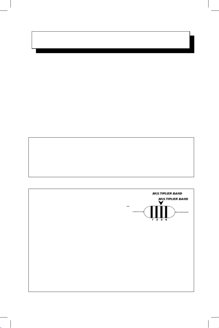
Table 1-C
Diode Identification Guide
The main board uses eight 1N 4 148 diodes easily recognized as identical
to the four diodes installed on the Display Board. The Zener, and Varactor
diodes must be identified exactly. Here's some help:
TYPE Body Type/Color Cathode Band
1N4148 (8) Glass, copper-color inside Black
Zener (3) Silver-gray Grayish black
BA479 (2) Glass Black Grey
Table 1-D
F. Model 1254 Receiver
Parts ldentification Notes
We r ely on you to know already what a resistor, transistor, lC
"chip" and other common electronic parts "look like."
REMINDER: Both the back and inside front covers of this manual
provide some light-hear ted help on basic parts identification.
Each assembly step provides useful help in identifying any part,
whether by shape, color-code, manufacturer's markings, or other
description.
Since correct parts installation is the key to this Receiver working
perfectly, we encourage you to refer to the following Parts
Identification Notes whenever you feel it necessary.
Table 1-A
RESISTORS:
The Main Board uses only 1/4-watt resistors, while the Display Board uses
smaller 1/8-watt resistors packed in the bag with the Display Board itself.
Each instruction step lists the first THREE color bands, assuming the fourth
band to be gold (5% tolerance). Just be careful about that third "multiplier"
band. For example, your kit uses 4.7, 47, 470, 4.7K and 47K resistors, each
for very different purposes.
Table 1-B
MOLDED INDUCTORS
(also c al l ed "CH0KES").
These parts are readily recognized because:
1. They are packed with other coils, transformers,
etc.
2. W hile similar to resistors, they have "bullet"-shaped ends.
3. The body consistently has a green-bluish color.
While these parts follow the resistor color code chart for value identification, we
will be the first to agree with you that these color bands really can be HARD to
read. EXAMPLE: red, orange and brown can each look like some shade of mud.
NO, your eyesight is NOT the problem!
We suggest:
1. Sort all the inductors by quantity required in the Parts List.
2. Set aside (and mark on paper) those which are completely clear to you.
3. Compare PAIRS of bands and pay close attention to the 3rd (multiplier) band
4. A "Process of Elimination" is the easiest way to resolve questions .
1254 – Getting Started – 15
Page 17
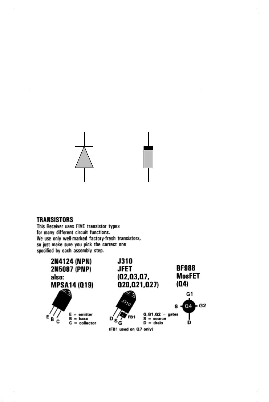
Table 1-C
Diode Identification Guide
The main board uses eight 1N 4 148 diodes easily recognized as identical
to the four diodes installed on the Display Board. The Zener, and Varactor
diodes must be identified exactly. Here's some help:
TYPE Body Type/Color Cathode Band
1N4148 (8) Glass, copper-color inside Black
Zener (3) Silver-gray Grayish black
6.2V marked “1N 75 3A- nnn” (D6, D7)
3.9V marked “1N 74 8A- nnn” (D17)
BA479 (2) Glass Black Grey
Cathode
Table 1-D
1254 Getting Started – 16
Page 18
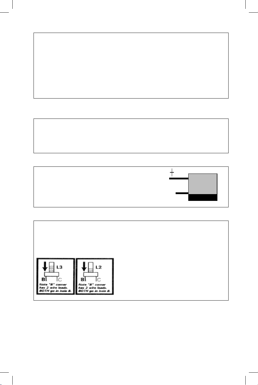
Table 1-E
protocol is to identify those in picofarads up to 99 pF simply as 1 pF or 33 pF, etc.
characteristics (e.g. 33J = 33 pF.)
If you've never built an electronics kit before, you are a GOOD
candidate for successful construction of this receiver - because
we think you'll rely on this instruction manual very diligently.
("Experienced" builders tend to be more inclined to shortcuts
which can lead to mistakes!)
Both this manual and the engineering discipline for this receiver
were done with YOU very much in mind. We won't insult you
by claiming that "anybody" can build this receiver: you'll
certainly need the knowledge and skills you gained by working
for your ham license or studying electronics theory, and you'll
want to allow for a little more assembly tim e than may he
needed by those with more building experience"
Aside from the willingness to follow the directions in this manual,
the main skill you need is that of soldering. Here, it's a ver y
good idea to get s ome practice before working on the receiver
circuit boards. Building some simpler T-KlT projects is, of
course, a great way to get into kit building. Another way is to
take a circuit board from any discarded radio or other electronics
device and then remove a number of parts by melting their solder
connections. Re-install some or all of the parts, doing so until
your solder connections look as clean and professional as the
factory work. Don't hesitate to ask an electronics repair
technician to critique your work or show you a few tips.
Kit-Building Tips . . .
1 . Please USE the bits of knowledge and wisdom capsulized on
the back c over of your T-KIT Instruct ion Manual! You'll find
resistor color-codes, soldering tips and more!
2. Unfamiliar Words: We try to use plain language throughout
this manual, but electronics does have its special terms and
abbreviations. A "glossary" useful to this receiver pr oject is
printed in the REFERENCE SECTION (Part 3) of this manual.
G. Building Electronic Kit Projects:
THE ESSENTIALS
CERAMIC DISC CAPACITORS
The vast majority of capacitors in this circuit are the ceramic disc type. Our
There may be one letter to identify temperature
From 100 pF (marked 101) on up to capacitors in the μF range, we provide the
exact part marking (101, 102, 103, 151, 181, etc.) minus any letter. All disc
capacitors are specified to fit the exact lead spacing on the board: if a
capacitor seems too big or too little for the spacing, you have selected the
wrong part!
Table 1-F
MYLAR FILM CAPACITORS
These capacitors have shiny, thick, rectangular bodies with value markings jus t
like on the ceramic disc capacitors. In this kit design, the mylar film parts (used in
the PLL filter and RF bandpass filter) have values different from any of the disc
capacitors, with the sole exception of C11, .01 μF.
Table 1-G
ELECTROLYTIC CAPACITORS
These cylinder shaped parts are easy to recognize
from their longer (+) leads and clearly marked wide
negative band. In this kit, just be sure to identify an
install correctly those smallest 1μF and 10μF
capacitors as specified in the directions.
Table 1-H
“SPECIAL” PARTS
“Special” parts include crystals, filters, balun transformers which are identified
clearly by a manufacturer's number on the part itself OR by detailed description in
a k i t assembly step. We give you plenty of help in the assembly ins tructions for
identifying and installing these parts correctly.
The VCO coils (Phase 3.0) are wound
on WHITE forms easily identified:
L3 (VCO-1): BROWN paint dot
L2 (VCO-2): RED paint dot
1254 – Getting Started – 17
Page 19
If you've never built an electronics kit before, you are a GOOD
G. Building Electronic Kit Projects:
THE ESSENTIALS
candidate for successful construction of this receiver - because
we think you'll rely on this instruction manual very diligently.
("Experienced" builders tend to be more inclined to shortcuts
which can lead to mistakes!)
Both this manual and the engineering discipline for this receiver
were done with YOU very much in mind. We won't insult you
by claiming that "anybody" can build this receiver: you'll
certainly need the knowledge and skills you gained by working
for your ham license or studying electronics theory, and you'll
want to allow for a little more assembly tim e than may he
needed by those with more building experience"
Aside from the willingness to follow the directions in this manual,
the main skill you need is that of soldering. Here, it's a ver y
good idea to get s ome practice before working on the receiver
circuit boards. Building some simpler T-KlT projects is, of
course, a great way to get into kit building. Another way is to
take a circuit board from any discarded radio or other electronics
device and then remove a number of parts by melting their solder
connections. Re-install some or all of the parts, doing so until
your solder connections look as clean and professional as the
factory work. Don't hesitate to ask an electronics repair
technician to critique your work or show you a few tips.
Kit-Building Tips . . .
1 . Please USE the bits of knowledge and wisdom capsulized on
the back c over of your T-KIT Instruct ion Manual! You'll find
resistor color-codes, soldering tips and more!
2. Unfamiliar Words: We try to use plain language throughout
this manual, but electronics does have its special terms and
abbreviations. A "glossary" useful to this receiver pr oject is
printed in the REFERENCE SECTION (Part 3) of this manual.
1254 – Getting Started – 18
Page 20
3. SOLDERING: If you are inexperienced, ask any electronics
WORTH REPEATING
Let the heated connection itself melt the solder, NOT the iron tip!
H. Model 1254 SWL Receiver
Kit Assembly OVERVIEW
technician to show you how it's done, then do practice
soldering/de-soldering on a junked circuit board before working
on your kit. Here's what is important:
Keep the soldering iron tip CLEAN, using a damp sponge
Let the heated connection itself melt the solder, not the iron tip
Use a thin diameter of rosin-core solder
Use VERY good lighting; NEVER be embarrassed to use a
magnifier!
4. DE-SOLDERING is the opposite of soldering and is a more
tedious procedure. Again, a repair technician can show you the
best technique. Take care not to damage circuit board pads or
traces - save yourself f rom desoldering agony by installing the
right part the right way the first time!
5. Except for P1 , P2 and J5 mounted on the bottom ("solder
side") of the board, ALL Main Board parts are inserted into the
top silkscreened side, with leads passing through the holes to t he
bottom solder side. (This advice m ay seem insulting, but some
folks DO carefully mount and solder all parts on the copper side
of the board and wonder why the kit won't work!)
6. Insert all parts as close to the board surface as possi ble before
soldering and trimming. Excess wire length above the board can
cause unwanted oscillations.
7. Reminder about your Kit Manual: NEVER "Solder first and ask
questions later" ! The Success of your project depends on your
willingness to study our published directions attentively. Check
your kit package for any update sheet(s) to supplement this
manual. Use the double check blocks to review your work
(ideally with someone else) before connecting voltage.
8. TOOLS: Page 14 lists the "minimum" tools needed f or this
particular project. However, you'll appreciate owning a more
varied collection of small tools for electronics work: the selection
at Radio Shack'" is good, with the lower-priced versions being
quite sufficient. If buying your first voltmeter ("multitester"), you
may find the "analog" meter type easier to use at first than the
digital type.
1254 – Getting Started - 19
Page 21
You will build the Display Board first and then occasionally plug it into
H. Model 1254 SWL Receiver
Kit Assembly OVERVIEW
the Main Board for further testing. To get a good fit of the LED's and 3digit displays, you'll be handling the front panel and display lens - be
VERY careful not to touch these with your soldering iron!
After finishing PHASE 2.0 (Logic and DC Power Input sections), the
powered-up Display Board plugged to the Main Board (via P1, P2) can
now simulate all receiver functions or features described in the Operating
Instructions in the Reference section, though not executing them.
Finishing PHASE 3.0 requires VCO coil adjustments done with a simple
voltmeter measurement at "VCO TP." Individual board drawings are
provided as a help for correct assembly of the two shielded VCO sections.
Completing Phase 4.0 lets you verify that the audio amplifier, product
detector and Second IF amplifier work properly. This Phase also includes
the AGC and uses the largest number of parts of any of the assembly
sections.
Phase 5.0: Finishing this section results in a non-tuneable receiver with
full s ensitivity capable of receiving a 45 MHz test signal , with the Clarifier
control operational. Mixing the 45 MHz 1st output with the 44.545 2nd LO
produces the 455 kHz signal detected and amplified in the Phase 4.0
circuitry. The receiver is designed to generate its own 45 M Hz test signal.
Phases 6.0 and 7:0: (RF Input and First Mixer sections, Final
Assembly): You're ALMOST ready to start using your receiver, so
don't rush these building phases! This work brings in the antenna
signals through the shielded Bandpass Filter circuitry to the First Mixer
(also s hi el ded), where received signals are mixed with the tuneable 45-75
MHz LO si gnal from the VCO's. This mixing results in a 45 MHz 1st IF
signal fed to the input of the circuitry you built in Phase 5.0. Very simple
alignment is done in Phase 7,0 with the receiver mostly assembled. The
result is a frequency-synthesized dual-conversion receiver rivaling radio
sets costing much more.
See following foldout page for details on the major
mechanical parts used to finish your receiver in Phase 7.0.
►
1254 – Getting Started – 20
Page 22
Before you do ANY soldering,
we remind you again to do the following:
Installing Parts on the Circuit Boards:
When we say "INSTALL" a part, this is what we mean:
Model 1254 Receiver
USE ROSIN.CORE SOLDER ONLY.
Kit Assembly
Steps and Illustrations
Installing parts on the boards
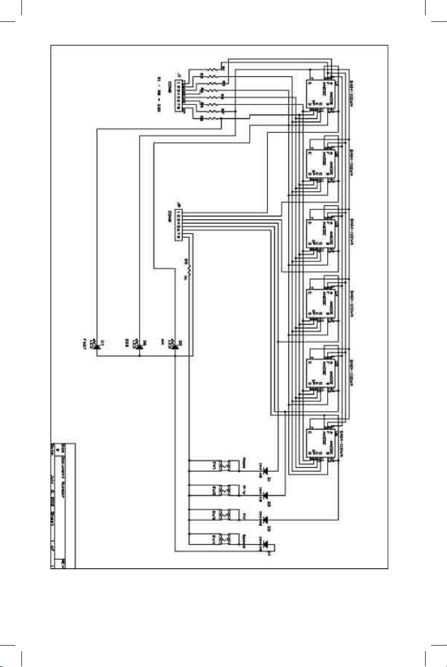
Preview of Display Board Assembly
Phase 1.0: Display Board Assembly
Sectional Schematic
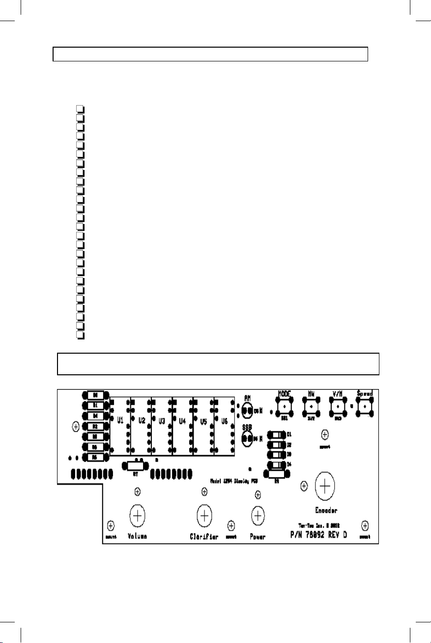
Parts Quic k-Reference and Display Board P ictorial
Step -by-Step Assembly
Notes on Main Board Assembly
Phase 2.0: Logic Section and Display Drivers
Sectional Schematic and Ci rcuit Board Pictorial
Quick-Reference Parts List
Step -by-Step Assembly
Note on Circuit Function Demonstrations
Phase 2.O Progress Test
Phase 3.0: VCO's and PLL ("Phase-Locked Loop")
Sectional Schematic and Ci rcuit Board Pictorial
Quick-Reference Parts List
Step -by-Step Assembly
Phase 3.0 Progress Test:
Phase 4.0: Receiver Audio, AM and Product Detectors,
455 kHz IF Amplifier, AGC circuit
Sectional Schematic and Ci rcuit Board Pictorial
Quick-Reference Parts List
Step -by-Step Assembly
Progress Tests: Audio, p. 41, IF amplifier, p. 45-46
Phase 5.0: 2nd Mixer, 2nd LO, Clarifier control
Sectional Schematic and Ci rcuit Board Pictorial
Quick-Reference Parts List
Step -by-Step Assembly
Progress Test:
Phase 6.0: RF Input, 1st Mi xer, 1st LO amplifier
Sectional Schematic
Quick-Reference Parts List
Bandpass filt er pictorial and assembly steps
First mixer pictorial and assembly steps
Installation of rem aining parts
6-10
11-12
14-15
16
17-20
21-22
23-24
26-27
28-29
30-33
34-35
36-37
38-39
40-45
48-49
50
51-53
54-55
56
57
58-59
60-61
62-63
2
3
4
5
Phase 7.0: Final Assembly and Alignment
Model 1254 Receiver Alignment
64-72
68-69
1254 – Assembly - 1
Page 23
Before you do ANY soldering,
USE ROSIN.CORE SOLDER ONLY.
we remind you again to do the following:
Check and or ganize your kit parts in whatever way
Is most convenient for you. A special IDENTIFICATION
GUIDE is provided after the Parts List.
Go through this ent ire manual: familiarize yourself
with its organization and illustrations.
Prepare a clean, well-lighted work space.
Study the ASSEMBLY OVERVIEW
(Getting Started Section, Page 20)
Build the Display Board FIRST. All its parts are packed
with the board itself, and it is a good orientation project.
Installing Parts on the Circuit Boards:
When we say "INSTALL" a part, this is what we mean:
Choose correct part value
Insert in correct PC Board location
Insert correctly, if there is a r ight way and wrong way
such as f or diodes, IC's,
electrolytic capacitors, transistors etc.
Insert the part as far as it can go into the board.
Solder all wires or pins
Trim or "nip" excess wire lengths
of a type intended for el ectronic PC-board assembly.
(Available at electronics distributors or Radio Shack" stores.)
DO NOT use hardware store solder, paste or flux,
Solder contains LEAD: wash hands before eating!
1254 – Assembly - 2
Page 24
Model 1254 SWL Receiver
PREVIEW of
Phase 1.0 Display Board Assembly
The Display Board is a useful "warmup" project before getting
started on the more complex Main Board. It will be plugged in
temporarily for Progress Tests in Phases 2.0 through 5.0 and
installed permanently at the end of Phase 6.0.
To help you make a good beginning, this Preview and Phase 1.0
assembly directions provide a bit more detail than will be needed
for most Main Board assembly steps. This board appears simple,
using only a handful of parts. However, correct construction is vital
to the success of this kit project and the reliability of your Model
1254 Receiver.
All parts used for the Display Board are packed together with the
board itself . Except for the common 1N4148 diode, all parts in the
Display Board kit are unique to this assembly phase, even the
resistors! (The display board uses 1/8 watt resistors, while all other
resistors are 1/4 watt.)
KIT PARTS REOUIRED for Phase 1.0:
Display Board Parts Kit
Model 1254 Front Panel
Model 1254 Front Panel Display Lens
PROCEDURES REOUIRED:
Installing all Display Board parts, with special attention to
directions for Display LED's U1-U6, LED's (D5-D7) and J1 , J2
Wiring and mounting of the ENCODER
Wiring and mounting of the D C Power Switch
(D5-D6)
1254 – Assembly - 3
Page 25
1254 – Assembly – 4
Page 26
PHASE 1.0: Display Board
All parts used for the Display Board are packed together with the
board itself . Except for the common 1N4148 diode, all parts in
the Display Board kit bag are unique to this assembly phase,
even the resistors! (The display board uses 1/8 watt resistors,
while all other resistors are 1/4 watt.)
All parts except J1 and J2 are mounted on what we will refer to
as the FRONT or silkscreened side of the display board, with
soldering done on the back side. J1 and J2 are mounted on the
back, soldered on the front.
INSTALLING U1-U6 DISPLAY LED MODULES:
one possible orientation on the board. Insert U1 in its board
position, making very sure all four support legs are squarely
seated on the board. Solder ONE pin in each row. Before further
soldering, CHECK carefully to make sure the display is squarely
against the board. If necessary, reheat and adjust the two
connections. Because of the length of the pins, you will
probably find it easiest to nip excess length after soldering each
pin, to provide clearance to s older the next connection. Solder
and nip all pins of U1.
Lay the receiver's molded front panel fac e down on a clean, non-
abrasive surface. (A dry wash cloth works nicely, or use the
packing foam from your kit.)
QUICK REFERENCE SUMMARY
PHASE 1.0
Display Board Assembly
CAUTION: To install the LED indicators, you will be working
with the receiver's front panel to get a good fit. Be VERY careful
with your soldering iron tip during these processes so as not to
scar (melt) the front panel!
EN1
D1
D2
D3
D4
D5
D6
D7
U1-U6
R1
R2
R3
R4
R5
R6
R7
R8
R9
SW1
SW2
SW3
SW4
S1
J1
J2
Encoder
1N4148
1N4148
1N4148
1N4148
Green LED
Green LED
Green LED
Display LED
33 ohm, 1/4watt
33 ohm, 1/4 watt
33 ohm, 1/4 watt
33 ohm, 1/4 watt
33 ohm, 1/4 watt
33 ohm, 1/4 watt
33 ohm, 1/4 watt
33 ohm, 1/4 watt
1K, 1/4 watt
momentary
“
“
“
SPDT Toggle
8-pin socket
8-pin socket
Phase 1.0: Display Board
Freq/Memory TUNE
pushbutton switch multiplexing diode
“
“
“
AM mode indicator
SSB mode indicator
FAST tuning mode indicator
frequency dis play
LED display current limiting
“
“
“
“
“
“
“
multiplexing resistor
MODE
MW
V/M
Tuning SPEED
DC power
mates P1 on main board
mates P2 on main board
1254 – Assembly – 5
Page 27
PHASE 1.0
Display Board Assembly
CAUTION: To install the LED indicators, you will be working
All parts used for the Display Board are packed together with the
board itself . Except for the common 1N4148 diode, all parts in
the Display Board kit bag are unique to this assembly phase,
even the resistors! (The display board uses 1/8 watt resistors,
while all other resistors are 1/4 watt.)
All parts except J1 and J2 are mounted on what we will refer to
as the FRONT or silkscreened side of the display board, with
soldering done on the back side. J1 and J2 are mounted on the
back, soldered on the front.
INSTALLING U1-U6 DISPLAY LED MODULES:
1-1. The pin arrangements of U1-U6 permit only
one possible orientation on the board. Insert U1 in its board
position, making very sure all four support legs are squarely
seated on the board. Solder ONE pin in each row. Before further
soldering, CHECK carefully to make sure the display is squarely
against the board. If necessary, reheat and adjust the two
connections. Because of the length of the pins, you will
probably find it easiest to nip excess length after soldering each
pin, to provide clearance to s older the next connection. Solder
and nip all pins of U1.
1-2. Install U2-U6 exactly as explained in 1-1 for U1.
with the receiver's front panel to get a good fit. Be VERY careful
with your soldering iron tip during these processes so as not to
scar (melt) the front panel!
1-3a. Preparation to install LED's:
Lay the receiver's molded front panel fac e down on a clean, nonabrasive surface. (A dry wash cloth works nicely, or use the
packing foam from your kit.)
1254 – Assembly – 6
Page 28
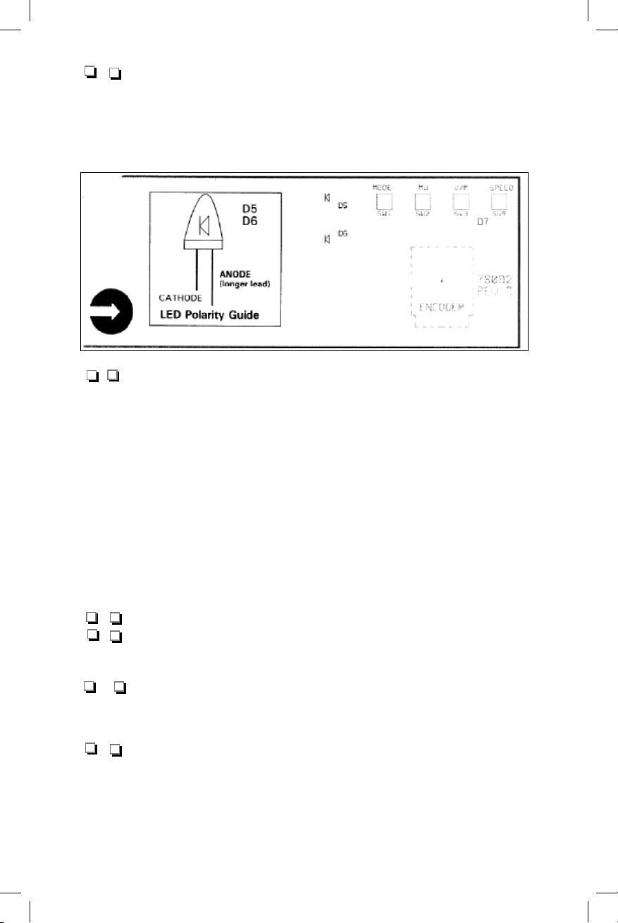
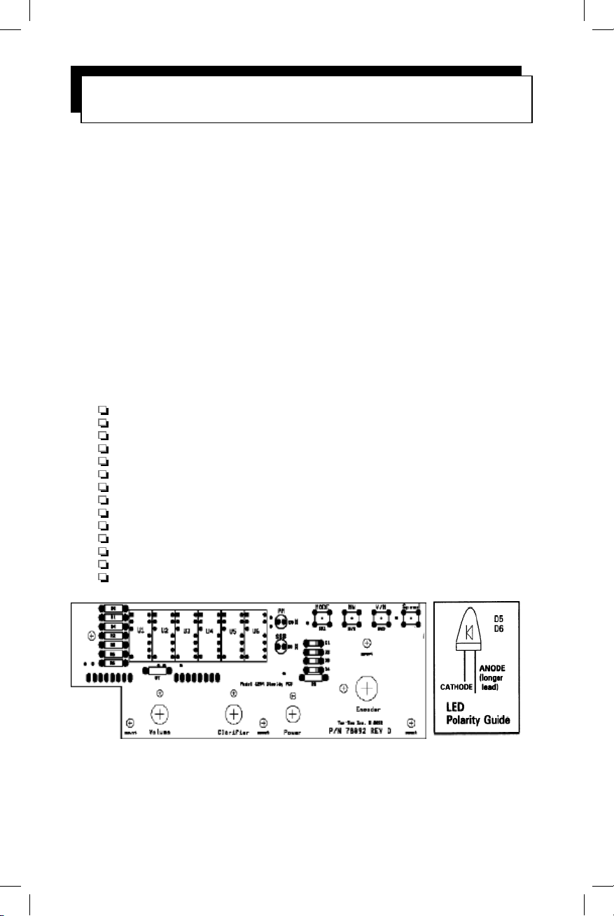
1-3b. Examine one of the small LEDs and the LED outlines
IMPORTANT: Examine these sockets and notice the row of
openings and tiny metal tabs on one side. These tabs will
protrude when the sockets are mated to plugs. Ther efore install
the sockets with the tab rows facing UP, so there is no chance
that extended spring tabs can short against the main board.
for squareness and resolder if necessary. Then solder the
remaining 6 pins; no trimming is required.
Install the following 1/8 watt resistors:
Install the following diodes, type 1N4148, making sure to
position the banded ends (cathodes) as outlined on the board:
but insert them carefully so as not to crumple any of the mount-
ing legs. Each switch must rest flush against t he surface of the
board. Solder all four pins for each switch.
illustrated in Figure 1.1 Notice that the anode and cathode ends
of the LED's are clearly silkscreened on the board. The anode is
the LONGER of the two LED leads.
Figure 1.1
1-4. LED Installation Procedure. First, insert all 3 LED's with
correct anode orientation per Step 1-3 and Fig. 1.1. Don't push
them in very far, because they need to extend into the front
panel for a good fit.
Seat the plastic lens for the 6-digit display in its panel position
and then lay the display board into the panel. (Remove the
protective paper from the lens.) While holding the board and
panel face down, slide all 3 LED's into their panel positions as far
as they can go. Solder ONE side of each LED and check front
panel for a good fit. Resolder any LED which needs adjusting
and then solder all remaining wires. Before trimming, check to
make s ure that all the longer anode leads are oriented in the
same direction per Fig. 1.1.
1-5. Green LED D5 installed per Steps 1-3 and 1-4.
1-6. Green LED D6 installed per Steps 1-3 and 1-4.
1-7. Green LED D7 installed per Steps 1-3 and 1-4.
1-8. Set aside the front panel and display lens
carefully so they will not be scratched.
INSTALLING SOCKETS J1 and J2:
1-9. Read First: Sockets J1 and J2 ar e inserted on the back
(non-screened) side of the display board and soldered on the
front. It is important that the edges of J1 and J2 be squarely
against the rear of the board to ensure a good fit to the rightangle pin plugs on the main board.
1254 – Assembly - 7
Page 29
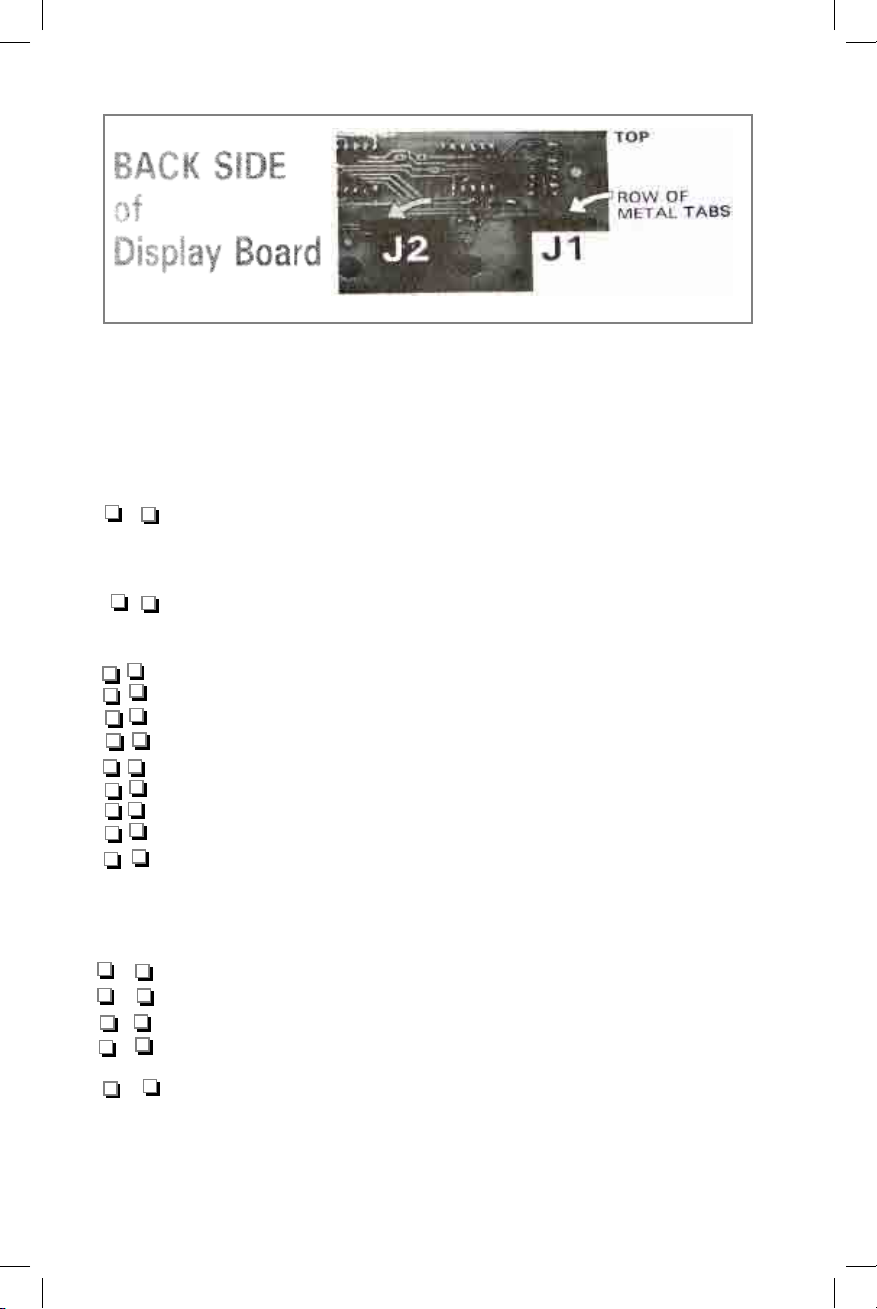
Figure 1.2
IMPORTANT: Examine these sockets and notice the row of
openings and tiny metal tabs on one side. These tabs will
protrude when the sockets are mated to plugs. Ther efore install
the sockets with the tab rows facing UP, so there is no chance
that extended spring tabs can short against the main board.
1-10. Insert socket J1 and solder the two end pins. Check
for squareness and resolder if necessary. Then solder the
remaining 6 pins; no trimming is required.
1-11. Install socket J2 exactly as explained in steps 1-9,10.
Install the following 1/8 watt resistors:
1-12. Resistor R1, 33 ohm (orange-orange-black).
1-13. Resistor R2, also 33 ohm.
1-14. Resistor R3, also 33 ohm.
1-15. Resistor R4, also 33 ohm.
1-16. Resistor R5, also 33 ohm.
1-17. Resistor R6, also 33 ohm.
1-18. Resistor R7, also 33 ohm.
1-19. Resistor R8, also 33 ohm.
1-20. Resistor R9, 1K (brown-black-red).
Install the following diodes, type 1N4148, making sure to
position the banded ends (cathodes) as outlined on the board:
1-21. Diode D1, type 1N4148.
1-22. Diode D2, type 1N4148.
1-23. Diode D3, type 1N4148.
1-24. Diode D4, type 1N4148.
1-25. The four push-button switches snap into place neatly,
but insert them carefully so as not to crumple any of the mounting legs. Each switch must rest flush against t he surface of the
board. Solder all four pins for each switch.
1254 – Assembly - 8
Page 30
1-26. Install switch SW1 (MODE) per Step 1-25.
on each of the two switch wires.
The bottom lug is identified per mounting done in step 1 -34.
connections.
aside until it is needed for various tests. It will be mounted
permanently after completion of the work in Phase 6.0. Do not
attempt to mount the fr ont panel to the display board until
instructed to do so in Phase 7.0.
1-27. Install switch SW2 (MW) per Step 1-25.
1-28. Install switch SW3 (V/M) per Step 1 -25.
1-29. Install switch SW4 (SPEED) per Step 1-25.
IMPORTANT SOLDERING TIP! Examine the Rotary Encoder:
regardless of whether the 3 silver terminals appear to you to be
tarnished, rub them anyway with a clean p encil eraser. This will
make for much easier soldering.
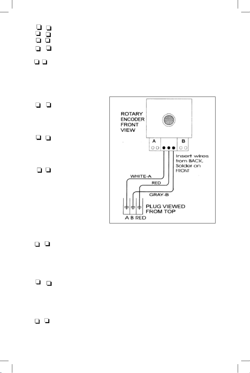
Figure 1.3. Encoder cable
connections
1-30. Strip 1/8" of
insulation from each of
the 3 wires of the
cable/plug assembly.
1-31. Study the
A-B markings on the
encoder and compare
to Figure 1.3.
1-32. The 3 wires
should be inserted from
the back and soldered
on the front side.
Insert the red wire and
the white A and gray B
wires EXACTLY how
Figure 1.3 depicts the
front of the encoder
and design of the plug.
1-33. Mount the rotary encoder to the display board with the
lock washer and nut provided. The washer goes on the front
side of the board. (If you wish, the large tuning knob may be
mounted temporarily to the encoder shaft for easy tuning dur ing
progress tests).
1-34. Mount the SPDT power switch on the display board.
Both the tabbed "alignment" washer and the lock washer should
be on the FRONT side of the display board. Be sure to get this
switch mounting and wiring done c orrectly, because you will be
instructed in Phase 5.0 to cut off the un-used switch lug.
1-35. Strip 1/8" insulation from the ends of both red wires of
the pre-assembled power switch cable.
1254 – Assembly - 9
Page 31

1-36. Cut two 1/2" lengths of insulating sleeve and slip one
on each of the two switch wires.
1-37. Solder one wire to the center lug of the SPDT switch.
1-38. Solder the other red wire to the bottom switch lug.
The bottom lug is identified per mounting done in step 1 -34.
1-39. Slide the insulating sleeves over t he completed switch
connections.
1-40. Double-check all your work and set the display board
aside until it is needed for various tests. It will be mounted
permanently after completion of the work in Phase 6.0. Do not
attempt to mount the fr ont panel to the display board until
instructed to do so in Phase 7.0.
1254 – Assembly – 10
Page 32
● About the Circuit Board Drawings:
The sectional circuit board drawings are adapted directly from
the silk-screening on the board itself, but they have been
modified in two important ways:
1. Component "designators" (C1, R1, Q1, etc.) are consistently
within the outline of the part for maximum convenience in
identifying a part's real location. On the board itself, many such
designators are off to the side , tor two reasons. First, screening
over plated holes is not good manufacturing practice. Second, it
helps to see some clear designators AFTER parts-installation is
finished.
2. USEFUL NOTES AND SKETCHES have been added to the
sectional board drawings. As needed, we ref er to these in the
Assembly Instructions.
● The Quick-Reference Summaries
A Quick Reference Summary of the parts used in each Assembly
Phase is printed at the beginning of the instructions for that
phase. It may be used first as a guide to gathering parts for this
phase. It is pr ovided as an extra help in double-checking
correctness of parts values with brief notes on the function of
each part. These summaries are adapted from the complete
Component Reference Index in the Reference Section of this
manual.
● Main Board Soldering Hints
In addition to all our nagging about avoiding solder bridges,
here's a tip about working with this double-sided board with
plated-through holes. Many of the solder pads are elongated
with two or more holes. W hen soldering a part to such a multi -
connection pad or connected group of pads, just be careful to
use the minimum solder needed for a good connec tion, because
it is VERY easy for excess solder to flow into an empty hole.
Such extra solder must be "de-soldered" before using that
mounting hole.
We discourage those "l know best" marathons in which "board-
stuffing" for t his whole receiver might be done in a long evening.
BUT we do NOT expect you to insert, solder and trim just one
part at a time. We suggest inserting 3-5 parts, bending the leads
to hold them well, double-check, then solder and trim. In
choosing the kit-building experience, we are not trying to
outpace the robotic manufacturing processes used at TEN-TEC
and worldwide!
Model 1254
Main Circuit Board Assembly
NEVER GUESS about the identification or orientation of a
part if it is not absol utely clear on the board silkscreen.
In discussing the Display Board, we referred to the "front" and
"back" sides of the board. In the Main Board assembly steps,
we will refer to the silkscreened side as the TOP and the solder
side as the BOTTOM. However, when the display board is
plugged in and facing you correctly, the component or top side
of the main board actually faces downward!
VERY IMPORTANT: Ta ke the time to s tudy the board itself and
all board drawings in this manual . Some silkscreened component
outlines or identifications may be obscured by the space required
for the plated-through pads. Therefore, you must consult the
circuit board outline drawings printed in this manual.
Conventions used
in this Instruction Manual
Our primary goal is accuracy of parts selection and correct
installation, NOT the fastest possible "stuffing" of the board.
That's why a numbered instruction is provided for each part, and
why we follow a specific pattern for listing instruction sequences
for similar groups of parts such as resistors or disc capacitors.
● Groups of similar parts:
Our assembly lists of similar parts begin with the lowest value of
resistance or capacitance, etc., and go up in value, grouping
identical values together, starting with the lowest designator
number. For example:
Install the following 1/4-watt resistors:
2-1. Resistor R1, 4.7 ohm (yellow-violet-gold).
2-2. Resistor R10, 470 ohm (yellow-violet-brown).
2-3. Resistor R4, 10K, (brown-black-orange).
2-5. Resistor R9, also 10K.
2-8. Resistor R5, 47K (yellow-violet-orange).
2-9. Resistor R6, also 47K.
2-10. Resistor R2, 10 megohm (brown-black-blue).
1254 – Assembly - 11
Page 33

● About the Circuit Board Drawings:
The sectional circuit board drawings are adapted directly from
the silk-screening on the board itself, but they have been
modified in two important ways:
1. Component "designators" (C1, R1, Q1, etc.) are consistently
within the outline of the part for maximum convenience in
identifying a part's real location. On the board itself, many such
designators are off to the side , tor two reasons. First, screening
over plated holes is not good manufacturing practice. Second, it
helps to see some clear designators AFTER parts-installation is
finished.
2. USEFUL NOTES AND SKETCHES have been added to the
sectional board drawings. As needed, we ref er to these in the
Assembly Instructions.
● The Quick-Reference Summaries
A Quick Reference Summary of the parts used in each Assembly
Phase is printed at the beginning of the instructions for that
phase. It may be used first as a guide to gathering parts for this
phase. It is pr ovided as an extra help in double-checking
correctness of parts values with brief notes on the function of
each part. These summaries are adapted from the complete
Component Reference Index in the Reference Section of this
manual.
● Main Board Soldering Hints
In addition to all our nagging about avoiding solder bridges,
here's a tip about working with this double-sided board with
plated-through holes. Many of the solder pads are elongated
with two or more holes. W hen soldering a part to such a multi connection pad or connected group of pads, just be careful to
use the minimum solder needed for a good connec tion, because
it is VERY easy for excess solder to flow into an empty hole.
Such extra solder must be "de-soldered" before using that
mounting hole.
We discourage those "l know best" marathons in which "boardstuffing" for t his whole receiver might be done in a long evening.
BUT we do NOT expect you to insert, solder and trim just one
part at a time. We suggest inserting 3-5 parts, bending the leads
to hold them well, double-check, then solder and trim. In
choosing the kit-building experience, we are not trying to
outpace the robotic manufacturing processes used at TEN-TEC
and worldwide!
1254 – Assembly - 12
Page 34

● This space is for your notes
Phase 2.0 Schematic Diagram Details
1254 – Assembly - 13
Phase 2.0 Assembly
begins on page 14 ►
Page 35
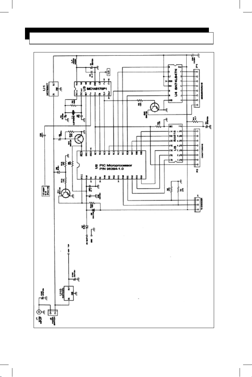
Phase 2.0 Schematic Diagram Details
1254 – Assembly - 14
Page 36
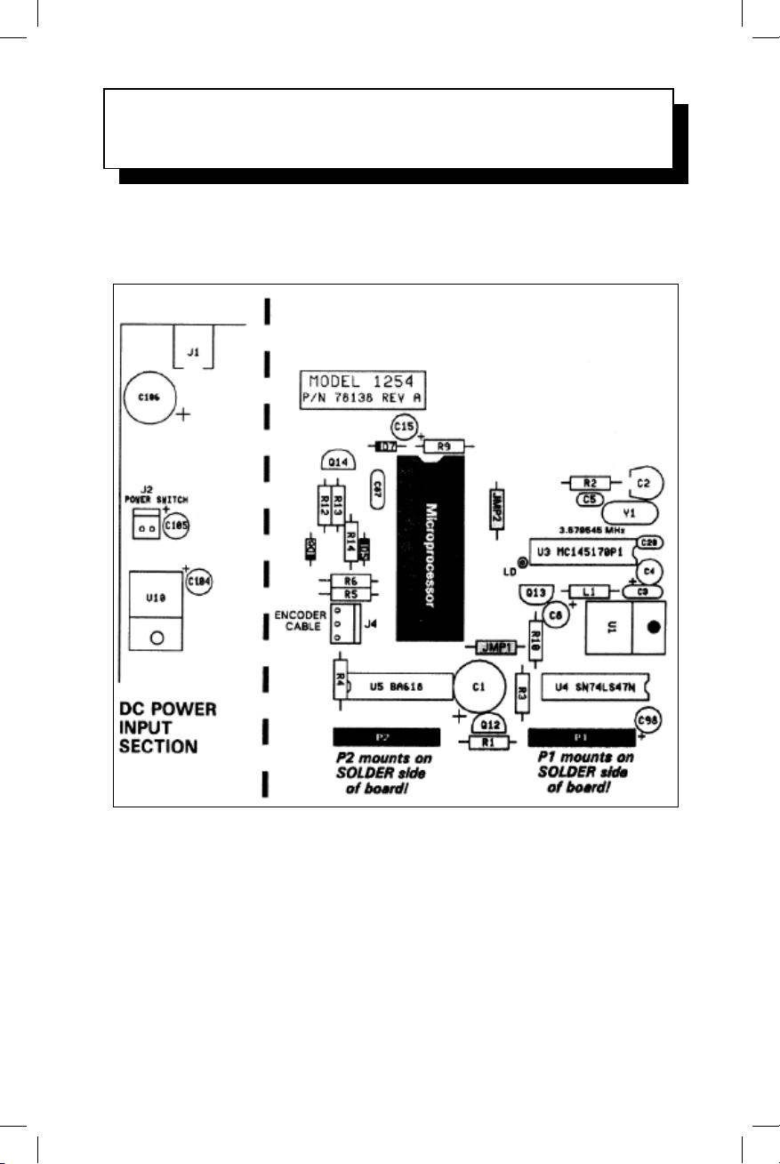
Phase 2.0: Frequency Synthesizer and DC Input
Phase
2.0
and DC Power Input Circuits
QUICK REFERENCE SUMMARY
Display Driver, Microprocessor
PLL synthesizer IC U3 and some of its supporting parts are
included, in this phase because its 3.580 MHz reference oscillator
also supplies the microprocessor clock signal.
1254 – Assembly - 15
Page 37
QUICK REFERENCE SUMMARY
Phase 2.0: Frequency Synthesizer and DC Input
470/16v el.
C1
5-40 pF var.
C2
0.1μF
C3
33/16v el.
C4
33pF
C5
1/50v el.
C8
33/16v el.
C15
.001μF
C20
.01μF
C87
10/25v el.
C98
33/16v el.
C104
33/16v el.
C105
470μf/16v el.
C106
1N4148
D5
6.2V zener
D6
6.2V zener
D7
DC jack
J1
2-pin
J2
3-pin
J4
100 μH
L1
8-pin header
P1
8-pin header
P2
2N4124
Q12
2N4124
Q13
2N4124
Q14
4.7 ohms
R1
10 megohm
R2
10K
R3
10K
R4
47K
R5
47K
R6
10K
R9
470
R10
10K
R12
10K
R13
10K
R14
MC7805CT
U1
(U1 also may be LM340T-5)
PIC16C57
U2
28-pin DIP socket for U2
(U2)
Microprocessor
MC145170P
U3
SN74LS47N
U4
BA618
U5
NJM7810A
U10
3.579546 MHz
Y1
“zero ohm resistor“ (black band)
JMP1
“zero ohm resistor” (black band)
JMP2
Filter Cap for display driver
Trimcap for master clock (adjust to 3.58 MHz)
Bypass on PLL chip
Bypass on PLL chip
Shunt cap on clock crystal
Reset coupling cap
Vdd supply bypass for μP
Couples PLL to VCO circuits
Supply bypass for U2
Supply bypass on U4
Bypass on output of U10
Bypass on input of U10
Main DC input bypass
Supply summing diode for U2
Supply turn-off detector
Backup battery summing diode
Coaxial DC power connection
DC power switch connection
Encoder cable connection
RFC for U3 DC supply
Mates Display Board J1 (install on solder side!)
Mates Display Board J2 (install on solder side!)
Decimal point current sink
Power-on reset transistor
Power-down detector
Supply lead to U5
Clock oscillator for U3
Display decimal point
Pull-down for pushbuttons
Pull-down for encoder
“ “
Pull-up for reset pin
Pull-down for Q13
Power-off detector
Power-off detector
Pull-up on RTCC pin
5V regulator for synthesizer circuitry
8-bit microprocessor (P/N 98384)
PLL synthesizer
LED segment driver
Digit driver
10V voltage regulator
Synthesizer clock set to 3.58 MHz (use base
insulator)
1254 – Assembly – 16
Page 38
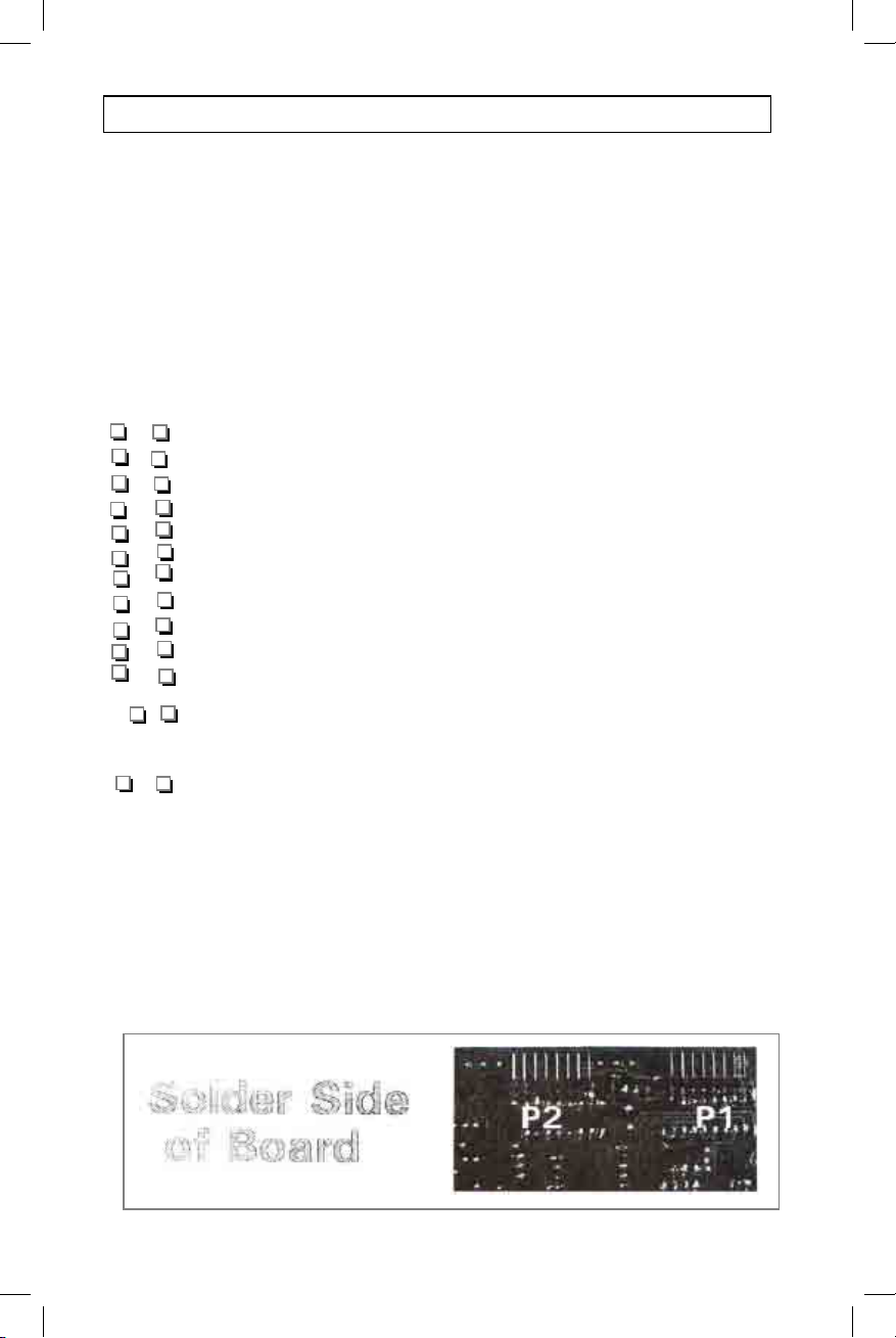
microprocessor, with the notched end aligned per the notch
outlined on the board. Insert carefully, making sure all pins mate
their holes with no pin bent back under the socket. Use good
lighting and a clean solder tip to avoid making solder bridges.
Do NOT insert U2 until instructed to do so.
or dotted end is oriented toward the right-side edge of the board
as designated by the notch outlined on the board.
dotted end is oriented as outlined on the board.
notched or dotted end is oriented as outlined on the board.
Solder U5 directly to the board; do not use a socket.
5), into its position as far as you can push it. Then bend it back
so that its heatsink and hole line up with the groundplane area
and m ounting hole in the board. Later, a screw will be secured
through U1 to the aluminum side panel.
Install the following ceramic disc capacitors:
Review Table 1-C in “Getting Started” as needed before
installing diodes D5, D6, and D7 in the following steps:
polarity as outlined on the board.
cathode polarity as outlined on the board.
cathode polarity as outlined on the board.
Phase 2.0 Assembly Steps
Before You Start: A Quick Referen ce Summary of the parts used
in Phase 2.0 is printed on page 16. It may be used first as a
guide to gathering parts for this phase. It is provided as an extra
help in double-checking correctness of parts values with brief
notes on the function of each part.
CAUTION!
Do NOT at tempt to install P1 and P2 until instructed to do so
and you understand the directions thoroughly.
Install the following ¼-watt resistors:
2-1. Resistor R1, 4.7 ohm (yellow-violet-gold)
2-2. Resistor R10, 470 ohm (yellow-violet-brown)
2-3. Resistor R3, 10K (brown-black-orange)
2-4. Resistor R4, also 10K.
2-5. Resistor R9, also 10K.
2-6. Resistor R12, also 10K.
2-7. Resistor R13, also 10K.
2-8. Resistor R14, also 10K.
2-9. Resistor R5, 47K (yellow-violet-orange).
2-10a. Resistor R6, also 47K.
2-10b. Resistor R2, 10 megohm (brown-black-blue).
2-11. Install electrolytic capacitor C98, 10 μF, being sure to
insert the longer ( + ) lead as shown on the board.
2-12. READ FIRST : When installing the right-angle headers
(P1 and P2), it is important that they sit squarely against the
board for a good fit to the display board. VERY IMPORTANT:
P1 and P2 are MOUNTED on the BOTTOM side of the board
as illustrated below and should be soldered from the top side.
Installing P1 at this time presumes that R3 and C 9 8 are already
installed, making the holes used for P1 perfectly clear w hen
viewed from the bottom side of the board.
Fig. 2.1: Installation of P1 and P2 on solder side of board
1254 – Assembly – 17
Page 39
2-13. Ins tall right-angle header P1 per Step 2-12.
2-14. Ins tall right-angle header P2 per Step 2-12.
2-15. Ins tall the 28-pin DIP socket s uppl i ed for the U2 PIC
microprocessor, with the notched end aligned per the notch
outlined on the board. Insert carefully, making sure all pins mate
their holes with no pin bent back under the socket. Use good
lighting and a clean solder tip to avoid making solder bridges.
Do NOT insert U2 until instructed to do so.
2-16. Ins tall U4, type 74LS47N, making sure that its notched
or dotted end is oriented toward the right-side edge of the board
as designated by the notch outlined on the board.
2-17. Ins tall U5, type BA618, making sure that its notched or
dotted end is oriented as outlined on the board.
2-18. Ins tall U3, type MC145170P1, making sure that its
notched or dotted end is oriented as outlined on the board.
Solder U5 directly to the board; do not use a socket.
2-19. Slide voltage regulator U1, type 7805CT (or LM340T-
5), into its position as far as you can push it. Then bend it back
so that its heatsink and hole line up with the groundplane area
and m ounting hole in the board. Later, a screw will be secured
through U1 to the aluminum side panel.
2-20. Solder and trim the 3 leads of voltage regulator U1.
Install the following ceramic disc capacitors:
2-21. Capacitor C5, 33 pF.(narrow lead spacing,
NOT the 33 pF capacitors used tor C21 ,C22, etc.).
2-22. Capacitor C20, .001 μF (marked 102).
2-23. Capacitor C3, 0.1 μF (marked 104).
2-24. Capacitor C87, also 0.1 μF.
Review Table 1-C in “Getting Started” as needed before
installing diodes D5, D6, and D7 in the following steps:
2-25. Ins tall diode D5, type 1N4148, with correct cathode
polarity as outlined on the board.
2-26. Ins tall 6.2V zener diode D6, type 1N753A, with correct
cathode polarity as outlined on the board.
2-27. Ins tall 6.2V zener diode D7, type 1N753A, with correct
cathode polarity as outlined on the board.
1254 – Assembly – 18
Page 40
2-28. Ins tall JMP1 , a "zero ohm resistor" (one black band.)
28. DC Power Circuitry
The following parts are installed near the left rear of the board.
side toward the back end of the board as outlined and illustrated
in Figure 2.2.
Figure 2.2
goes between the nut and bottom side of board. ) NOTE: the stiffness of
the leads will make it almost impossible for the part to lay perfectly flat on
the board. This is OK
Solder all three leads and trim away the excess lengths.
2-29. Ins tall JMP2 per step 2-28.
2-30. Ins tall electrolytic capacitor C1,470 μF, being sure to
insert the longer ( + ) lead as shown on the board.
2-31a. Ins tall electrolytic C4, 33 μF per Step 2-30.
2-31b. Ins tall electrolytic C15, also 33 μF.
2-32. Ins tall electrolytic C8, 1μF per Step 2-30. (Be careful
not to mix up the small 1 μF and 10 μF electrolytics.)
2-33. Ins tall trimmer capacitor C2; its flat side faces R2 as
shown on the board. Insert the part gently so as not to bend its
mounting terminals.
2-34. Slip a crystal base insulator over the leads of crystal
Y1, 3.579545 MHz. This insulator is white or clear plastic in the
shape of the crystal base.
2-35. Ins tall crystal Y1, making sure you select the 3.579
MHz crystal and not Y3 to be used in the 1st IF section.
2-36. Ins tall transistor Q12, type 2N4124, with the flat side
toward R1 as outlined on the board.
2-37. Ins tall transistor Q13, type 2N4124, with the flat side
toward U3 as outlined on the board.
2-38. Ins tall transistor Q14, type 2N4124, with the flat side
oriented as outlined on the board.
2-39. Ins tall the three-pin terminal J4 with the vertical locking
tab toward the socket for U2 as outlined on the board.
2-40. Ins tall L1 , 100 μH RF choke (brown-black-brown-gold).
2-41. Double-chec k all work you have done so far.
2-42. Remove the PIC microprocessor from its protective
Foam, check al l 28 pins for straightness, and straighten any pin
which appears to need it. Insert U2 into its socket with the
notched end toward D7 as plainly outlined on all drawings and
the board silksc reen.
1254 – Assembly – 19
Page 41
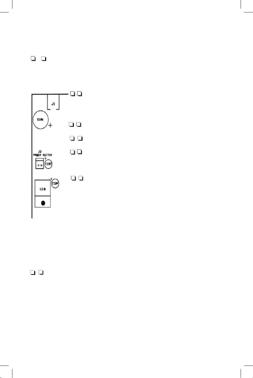
28. DC Power Circuitry
The following parts are installed near the left rear of the board.
2-43. Install the two-pin terminal J2 with the vertic al locking
side toward the back end of the board as outlined and illustrated
in Figure 2.2.
Figure 2.2
2-44. Install electrolytic capacitor C106, 470 μF,
being sure to insert the l onger ( + ) lead as
shown on the board.
2-45. Install electrolytic C104, 33 μF per Step 2-44.
2-46. Install electrolytic C105, 33 μF per Step 2-44.
2-47. Install coaxial DC connector J1: use sufficient
soldering heat to ensure a solid, shiny mechanical
bond from each lug to the plated circuit board holes.
2-48. Voltage regulator U10, typeNJM7810A,
resembles U1 in style, but the lead dimensions
differ. Using needle-nose pliers as needed, shape the
wide parts of the three leads so that U10's mounting
hole lines up with the hole in the board. After shaping
the leads, mount U10 to the board using the 3/8" #440 screw, lockwasher and #4-40 nut. (This is the
longest screw used in the kit and the lock washer
goes between the nut and bottom side of board. ) NOTE: the stiffness of
the leads will make it almost impossible for the part to lay perfectly flat on
the board. This is OK
2-49. Install the 10 volt regulator U10 as explained in 2-48.
Solder all three leads and trim away the excess lengths.
1254 – Assembly - 20
Page 42
OPTIONAL: For Educators and Experimenters
Phase 4.0: 455 kHz 2nd IF
An RF signal generator tuned to 455 kHz can be coupled to
the input of U7 at C40 after completing Phase 4B.
A nearby general coverage HF receiver or transceiver can be tuned to 455 kHz to
confirm oscillation of ceramic resonator Y2. NO adjustment on the 1254 b oard is
required or provided for.
An RF signal generator tuned to 455 kHz can used as a short-range "transm itter" (1
to 3 feet) after completing Phase 4C. Connect a foot or two of wire to serve as
its "transmitting antenna."
Find the CENTER pad for T7 (not yet installed) in the row of 3 pads nearest J5/J6.
Here, you will simply touch a test probe from your meter to serve as a "receiving
antenna." lt does not matter whether the test lead is connected to your meter.
With this set-up, the 1254 shoul d easily detect the nearby 455 kHz test signal.
(Coincidentally, the T-KIT Model 1050 "Universal BFO', with its tuneable 452-457
kHz output, works very nicely for such demonstrations.)
Phase 5.0: 45 MHz 1st IF
At this point the receiver can easily detect the output of an RF signal generator
tuned to 45 MHz.
REMINDER: This is the ONLY discussion in this manual of what
we consider to be optional circuit section demonstrations for
those builders or educators who wish them. They are not
needed in the Progress Tests.
Circuit Stage Demonstrations
Each Phase of the receiver construction process adds several related circuit stages.
In most cases, these circuit sections are capable of "doing something" of possible
interest to you if connected to external test equipment of some kind. For example,
you can hear an oscillator signal using another receiver, 0r use a signal generator to
hear that an IF section is working.
Each Assembly Phase for your recei ver kit includes "Progress Test" procedures. Our
goal in such tests is to verify that the completed circuit section simply "works" as
engineered. We specify the simplest possible testing to do this, such as a meter
reading. From experience, we find it best not to include nonessential circuit
performance demonstrations as part of kit building Progress Tests.
Setting up a useful circuit demonstration may require more external equipment than
you have on hand or is really needed. The following testing suggestions are provided
for those builders who enjoy observing or dem onstrating what various sections of the
receiver can "do." These possible demonstrations ar e NOT mentioned in the Progress
Tests: it is up to YOU to return to this section of the manual after each Progress
Test and determine whether you want to try out these suggestions.
Phase 2.0: Frequency Synthesi zer
The 3.58 MHz clock oscillator may be heard using another receiver tuned to that
frequency. C2 may be adjusted to exactly 3.5800 MHz using this method. The real
adjustment of C2 is done with the receiver completed and tuned to WWV.
Phase 3.0: 45-75 MHz local Oscillator and PLL
The synthesized LO tunes 45 MHz above the frequency indicated on the display, i.e.
45-75 MHz. In addition to the option of checking the LO output with a frequency
counter, the LO signal may be heard with any receiver capable of tuning in the 45-75
MHz range. Even an ordinary TV set can be used. simply run a jumper wire fro m
the "FREQ TIP" to the VHF antenna input and tune the 1254 per the following table:
Display
0.000.0
0.100.0
5.000.0
10.250.0
14.750.0
16.250.0
21.750.0
22.250.0
26.750.0
LO Output (MHz)
45.000
45.100
50.000
55.250
59.750
61.250
65.750
67.250
71.750
NOTES
Test signal: 1
st
IF (Phase 5.0)
6 m eter ham band (50-54 MHz)
TV channel 2 video
TV channel 2 audio
TV channel 3 video
TV channel 3 audio
TV channel 4 video
TV channel 4 audio
1254 – Assembly - 21
Page 43

Phase 4.0: 455 kHz 2nd IF
An RF signal generator tuned to 455 kHz can be coupled to
the input of U7 at C40 after completing Phase 4B.
A nearby general coverage HF receiver or transceiver can be tuned to 455 kHz to
confirm oscillation of ceramic resonator Y2. NO adjustment on the 1254 b oard is
required or provided for.
An RF signal generator tuned to 455 kHz can used as a short-range "transm itter" (1
to 3 feet) after completing Phase 4C. Connect a foot or two of wire to serve as
its "transmitting antenna."
Find the CENTER pad for T7 (not yet installed) in the row of 3 pads nearest J5/J6.
Here, you will simply touch a test probe from your meter to serve as a "receiving
antenna." lt does not matter whether the test lead is connected to your meter.
With this set-up, the 1254 shoul d easily detect the nearby 455 kHz test signal.
(Coincidentally, the T-KIT Model 1050 "Universal BFO', with its tuneable 452-457
kHz output, works very nicely for such demonstrations.)
Phase 5.0: 45 MHz 1st IF
At this point the receiver can easily detect the output of an RF signal generator
tuned to 45 MHz.
REMINDER: This is the ONLY discussion in this manual of what
we consider to be optional circuit section demonstrations for
those builders or educators who wish them. They are not
needed in the Progress Tests.
1254 – Assembly - 22
Page 44
Phase 2.0 Progress Test
At this point, further testing of this circuitry consists simply of
just playing with it as much as You care to! For example, you
can turn to the Operating Instructions in the Reference Section
and try out the [MW] and [V/M] f unctions.
You can use the [MW] (Memory Write) function to store
frequencies in memory, but keep in mind that the stored
information will be lost when power is turned off, because the
memory backup battery is not yet in use.
DO NOT install the 9-volt memory battery snap until instructed to
do so in Phase 7.0. Its wires will not withstand all the boar d
handling yet to be done.
beginning Phase 3.0.
2-50. Carefully plug the Display board into the sockets on the
solder side of the board. With the display facing you correctly,
the solder side of the main board faces up.
2-51. Plug the encoder cable into J4.
2-52. Plug the power switch cable into J2.
2-53. Connect the 1 SVDC power supply module to J1.
2-54. Turn on DC power: the display should read 15.000.0
(MHz), and only the [AM] or [SSB] LED should be lit. If the
display reads differently, perform the Microprocessor Reset (also
explained in the Operating Instructions) as follows:
Turn off DC power
Press and hold both the [Mode] and [MW] switch buttons
Turn on DC power
Release the switch buttons
2-55. Press the [MODE] button to select SSB mode and turn
the encoder shaft or knob slightly clockwise: the display should
advance to 15.002.5, 15.005.0, 15.007.5 and so forth in 2.5
kHz steps. lf the displayed frequency went DOWN (i.e. to
14.997.5, etc.), this means that the A and B wires to the
encoder are reversed. lf this is so, t urn off DC power and fix
that problem before proceeding.
2-56. Press the IMODE] button to s elect AM mode; turning
the encoder shaft should advance the display in 5 kHz steps,
such as 15.010.0, 15.015.0, 15.020.0, etc.
2-57. Press the [SPEED] switch button. The "FAST" LED
below it should light up, and you should observe tuning in 100
kHz steps such as 15.100.0, 15.200.0, etc. You will notice that
only a few gentle turns of the tuning control shaft easily moves
you several MHz in either direction.
2-58. Set your VOM or DVM to read DC voltage. Locate the
"10V TP" test point and measure the voltage between that pad
and ground. Any of the four mounting holes on the boar d is a
convenient ground. The reading should be about 10 volts DC.
1254 – Assembly - 23
Page 45

At this point, further testing of this circuitry consists simply of
just playing with it as much as You care to! For example, you
can turn to the Operating Instructions in the Reference Section
and try out the [MW] and [V/M] f unctions.
You can use the [MW] (Memory Write) function to store
frequencies in memory, but keep in mind that the stored
information will be lost when power is turned off, because the
memory backup battery is not yet in use.
DO NOT install the 9-volt memory battery snap until instructed to
do so in Phase 7.0. Its wires will not withstand all the boar d
handling yet to be done.
2-60. Unplug and set aside the front display board before
beginning Phase 3.0.
1254 – Assembly - 24
Page 46

This space is for your notes
Phase 3.0 Schematic Details
1254 – Assembly - 25
Phase 3.0 Assembly
begins on page 26 ►
Page 47
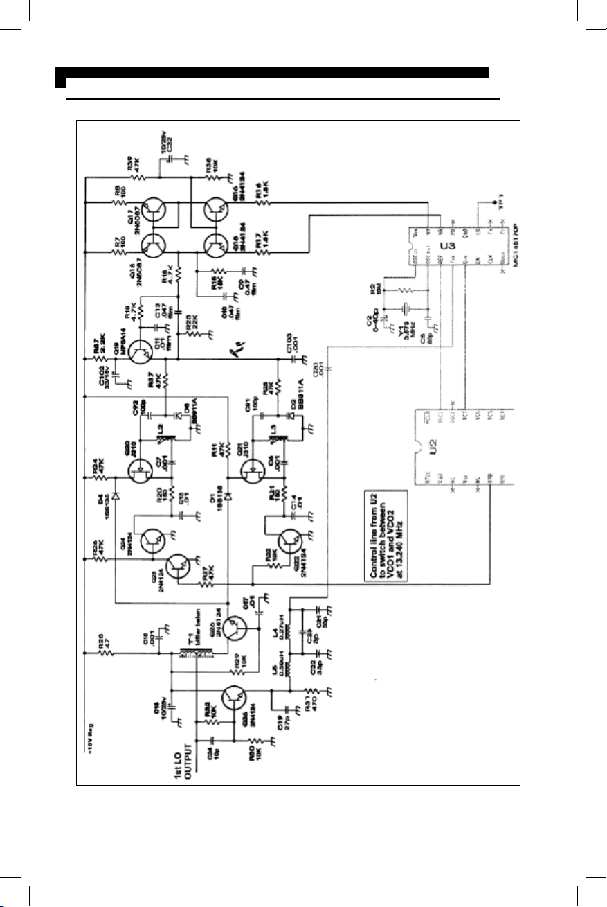
Phase 3.0 Schematic Details
1254 – Assembly - 26
Page 48
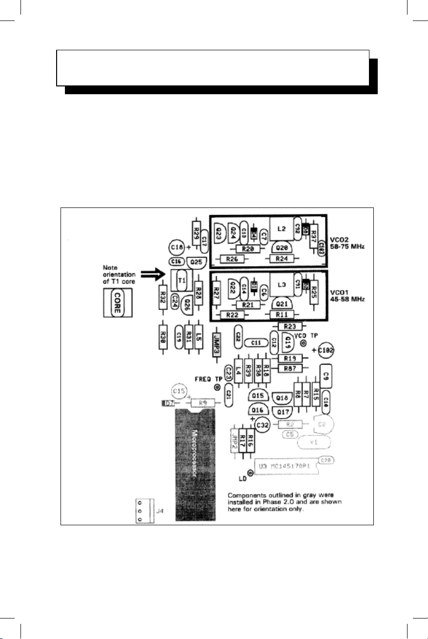
QUICK REFERENCE SUMMARY
Phase 3.0: VCO's and PLL Circuit
Phase
3.0
VCO's and PLL Circuit
The VCO's (Voltage Controlled Oscillators) will be permanently
enclosed in metal shields only after their operation is thoroughly
verified in Phase 7.0. Four different transistor types are used in
Phase 3.0: be sure to identify them correctly and to orient them
as outlined on the board. Consult Figures 3.1 and 3.2 carefully
as you work on the VCO's, which we'll do first.
1254 – Assembly - 27
Page 49
QUICK REFERENCE SUMMARY
Phase 3.0: VCO's and PLL Circuit
C6
C7
C9
C10
C11
C12
C13
C14
C16
C17
C18
C19
C20
C21
C22
C23
C24
C32
C91
C92
C102
C103
D1
D2
D4
D8
JMP3
L2
L3
L4
L5
Q15
Q16
Q17
Q18
Q19
Q20
Q21
Q22
Q23
Q24
Q25
Q26
R7
R8
R11
R15
R16
R17
R18
R19
R20
.001μF
.001μF
0.47μF film
.047μF film
.01μF film
.047μF film
.01μF
.01μF
.001μF
.01μF
10/25v el.
27 pF
.001μF
33 pF
33 pF
3 pF
10 pF
10 μF el.
100 pF
100 pF
33/16v el.
.001μF
1N4148
Factory Installed
1N4148
Factory Installed
“0 ohm”
VCO coil
VCO coil
0.27μH
0.39μH
2N4124
2N4124
2N5087
2N5087
MPSA14
J310
J310
2N4124
2N4124
2N4124
2N4124
2N4124
100
100
47K
15K
1.5K
1.5K
4.7K
4.7K
150
DC block on VCO
“ “
PLL loop filter
“ “ “
PLL active filer
“ “ “
VCO bypass cap
“ “ “
Supply bypass for Q25
Base bypass for Q25
Supply bypass for Q25
VCO bypass filter
VCO coupli ng cap to PLL
VCO lowpass filter
VCO lowpass filter
VCO lowpass filter
Coupling cap into Q26
Base bypass on charge pump
VCO varactor coupling cap
“ “ “ “
Collector bypass on Q19
RF bypass on VCO tuning line
VCO switching diode
VCO switching diode
circuit board jumper
VCO-2 coil
VCO-1 coil
PLL feedback lowpass filter
“ “ “ “
PLL charge pump
“ “
“
“ “ “
“ “ “
PLL active loop filter
VCO-2
VCO-1
VCO enable transistor
“ “
“ “
First LO amplifier
VCO buffer for PLL
PLL Charge pump
PLL Charge pump
Pull-up for VCO
PLL damping resistor
Charge pump input
Charge pump input
Active loop filter input
Active loop filter
VCO source resistor
1254 – Assembly - 28
Page 50
Phase 3.0 QUICK REFERENCE SUMMARY, cont.
This receiver uses two voltage-controlled oscillator (VCO) circuits
to cover the total tuning range. We'll begin with VCO-1 which
uses adjustable coil L3 to tune the 45-58 MHz 1st LO range.
3A. VCO-1 Com ponents
is the VCO c oil with the gr eater number of windings. The "B"
corner has two wire leads, as indicated in Figure 3.1.
3.1. Before soldering, make sure the coil base is seated FIR MLY
against the board. A solid mechanical fit is needed for these VCO
coils to minimize vibration.
Refer to PARTS IDENTIFICATION GUIDE for help in identifying
diode D1
R21
R22
R23
R24
R25
R26
R27
R28
R29
R30
R31
R32
R37
R38
R39
R87
T1
150
10K
22K
47K
47K
47K
47K
47
10K
10K
470
10K
47K
10K
47K
2.2K
bifilar bal un
VCO source resistor
VCO select
Active loop filter emitter
VCO pull-up resistor
Varactor bias resistor
VCO switching
VCO switching
Supply resistor for Q25
Base bias for Q25
Bias for Q26
Emitter resistor for Q26
Bias resistor for Q26
Varactor bias resistor
Charge pump bias
Charge pump bias
Collector feed for Q19
LO output
1254 – Assembly – 29
Page 51
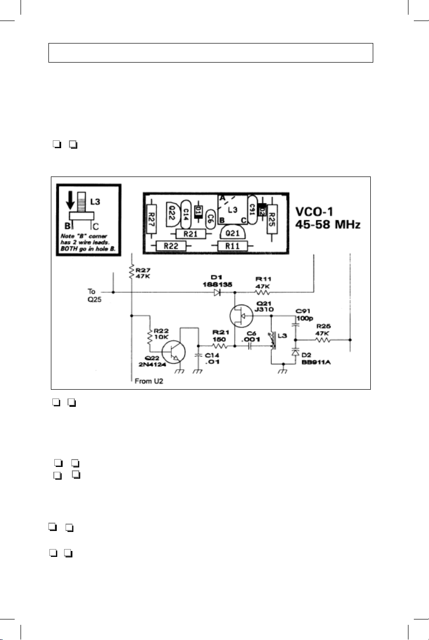
Phase 3.0 Assembly
This receiver uses two voltage-controlled oscillator (VCO) circuits
to cover the total tuning range. We'll begin with VCO-1 which
uses adjustable coil L3 to t une the 45-58 MHz 1st LO ran ge.
3A. VCO-1 Com ponents
Adjustable coil L3 is marked with a brown paint dot and
is the VCO c oil with the gr eater number of windings. The "B"
corner has two wire leads, as indicated in Figure 3.1.
3-2. Identify and install VCO coil L3 per step 3-1 and Fig.
3.1. Before soldering, make sure the coil base is seated FIR MLY
against the board. A solid mechanical fit is needed for these VCO
coils to minimize vibration.
3-3. Identify and install JFET transistor Q21, type J310.
3-4. Identify and install NPN transistor Q22, type 2N4124.
Refer to PARTS IDENTIFICATION GUIDE for help in identifying
diode D1
3-5. Diode D2 is factory installed.
3-6. Identify and install PIN diode D1, type 1N4148.
1254 – Assembly – 30
Page 52
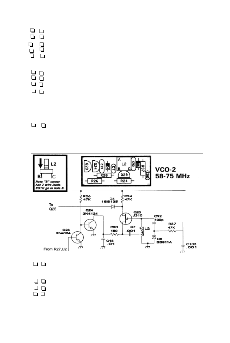
Install the following resistors:
Install the following resistors:
Install the following disc capacitors:
parts within the shield enclosures . Recheck component selection
and the quality of solder connections before proceeding. Do NOT
install the shielding until instructed to do so.
3C. PLL Circuit Completion
and its silkscreen outline on the board. The oblong ferrite core of
T1 must be or iented as outlined on the board and noted in the
drawing on page 27.
Install the following 1/4 watt resistors:
1/4-watt resistors, cont.
3-7. Resistor R21, 150Ω (brown-green-brown).
3-8. Resistor R22, 10K (brown-black-orange).
3-9. Install R11, 47K (yellow-violet-orange).
3-10. Install R25, also 47K.
3-11. Install R27, also 47K.
Install the following disc capacitors:
3-12. Capacitor C91,100 pF.(marked 101).
3-13. Capacitor C6, .001 μF (marked 102).
3-14. Capacitor C14, .01 μF (marked 103).
3-15, 16. reserved
38. VCO-2 Components
3-17. Adjustable coil L2 is the VCO coil with the fewer
number of windings and marked with a RED paint dot. The "B"
corner has two wire leads, as indicated in Fig ure 3.2.
Figure 3.2
3-18. Identify and install VCO coil L2 per step 3-17 and Fig.
3.2. Make sure the coil base is seated FIRMLY against th e board.
3-19. Identify and install JFET transistor Q20, type J310.
3-20. Identify and install NPN transistor Q24, type 2N4124.
3-21. Identify and install NPN transistor Q23, type 2N4124.
1254 – Assembly – 31
Page 53
3-22. Diode D8, is factory installed.
3-23. Identify and install PIN diode D4, type 1N4148.
Install the following resistors:
3-24. Resistor R20, 150Ω (brown-green-brown).
3-25. Resistor R24, 47K (yellow-violet-orange).
3-26. Resistor R26, also 47K.
3-27. Resistor R37, also 47K.
Install the following disc capacitors:
3-28. Capacitor C92, 100 pF.(marked 101).
3-29. Capacitor C7, .001 μF (marked 102).
3-30. Capacitor C103, also .001 μF.
3-31. Capacitor C13, .01 μF (marked 103).
3-32. The preceding steps complete installation of all VCO
parts within the shield enclosures . Recheck component selection
and the quality of solder connections before proceeding. Do NOT
install the shielding until instructed to do so.
3C. PLL Circuit Completion
3-33. Install PNP transistor Q17, type 2N5087.
3-34. Install PNP transistor Q18, also type 2N5087.
3-35. Install NPN transistor Q15, type 2N4124.
3-36. Install NPN transistor Q16, also type 2N4124.
3-37. Install transistor Q19, type MPSA14.
3-38a. Install NPN transistor Q25, type 2N4124.
3-38b. Install NPN transistor Q26, also type 2N4124.
3-39. Examine tr ansformer T1, the pre-ass embled bifilar balun
and its silkscreen outline on the board. The oblong ferrite core of
T1 must be or iented as outlined on the board and noted in the
drawing on page 27.
3-40. Install bifilar transformer T1 per 3-39.
Install the following 1/4 watt resistors:
3-41. Resistor R28, 47 ohm (yellow-violet-black).
3-42. Resistor R7, 100 ohm (brown-black-brown).
3-43. Resistor R8, also 100 ohm.
3-44. Resistor R31, 470 ohm (yellow-violet-brown).
3-45. Resistor R16, 1.5K (brown-green-red).
3-46. Resistor R17, also 1.5K.
3-47. Resistor R87, 2.2K (red-red-red).
1254 – Assembly - 32
1/4-watt resistors, cont.
Page 54
3-48. Resistor R18, 4.7K (yellow-violet-red).
which you will connect your voltmeter to do the L2 and L3 VCO
coil adjustments. lf more convenient for your test leads, you can
also solder a length of insulated hookup wire instead, and tr im it
shorter after c ompleting the adjustment.
already installed) to the pad marked "FREQ TP".
Adjustment of VCO c oils L2 and L3 r equires an alignment blade
of the CORRECT SIZE to fit the slot in the slug. A blade that is
too small can easily crack the slug. If you cannot find the right
size tool, use sandpaper to shape carefully the tip of a plastic
beverage stirrer or wooden kabob stick.
plug to J4 as in Phase 2.0 test ing.
switch plug to J2, and rec onnect the wall transformer power
supply t o J1.
the VCO test point and ground. You will be observing voltages
in the 2.5 to 8 volt range.
should read 15.000.0 MHz. If not, perform the Processor Reset
explained in the Operating Instructions (Reference Section) and
in the Phase 2.0 test.
L3 for a reading of 2.0 VDC at the VCO TP.
the VCO test point, there is a problem. Turn off DC power and
thoroughly recheck your work.
upward in frequency. You should observe a gradual rise in
voltage: about 4.5 volts at 7.000 MHz. The maximum will be
about 8.5 volts ± .5 volt at 13 .235 MHz.
3-49. Resistor R19, also 4.7K.
3-50a. Resistor R29, 10K, (brown-black-orange).
3-50b. Resistor R30, also 10K.
3-51. Resistor R32, also 10K.
3-52. Resistor R38, also 10K.
3-53. Resistor R15, 15K, (brown-green-orange).
3-54. Resistor R23, 22K (red-red-orange).
3-55. Resistor R39, 47K (yellow-violet-orange).
3-56. Install inductor L4, 0.27 μH (red-violet-silver-gold).
3-57. Install inductor L5, 0.39 μH (orange-white-silver-gold).
3-58. Install C9, the large mylar film 0.47 μF capacitor
(marked 474).
3-59. Install C10, the mylar film .047 μF capacitor (marked
473).
3-60. Install capacitor C12, also mylar film .047 μF.
3-61. Install C11, .01 pF mylar film (marked 103). [Be sure
to use a f ilm type capacitor, not ceramic disc for C11.]
3-62. Install electrolytic capacitor C32, 10 μF, with correct
(+ ) polarization as outlined on the board.
3-63. Install electrolytic capacitor C18, 10μF, per step 3-62.
3-64. Install electrolytic capacitor C102, 33μF, per step 3-62.
Install the following disc ceramic capacitors:
3-65. Capacitor C 23 , 3 pF.
3-66. Capacitor C24, 10 pF.
3-67. Capacitor C19, 27 pF.
3-68. Capacitor C21, 33 pF.
3-69. Capacitor C22, 33 pF.
3-70. reserved
3-71. Capacitor C16, .001 μF {marked 102).
3-72. Capacitor C17, .01 μF (marked 103).
3-73. Install "0 ohm" jumper JMP3.
3-74. Read entire text before soldering: Solder a 1/2" length
of bare wire (trimmed from a part already installed) to the pad
marked "VCO TP" near 019. This is the VCO Test Point to
1254 - Assembly - 33
Page 55
which you will connect your voltmeter to do the L2 and L3 VCO
coil adjustments. lf more convenient for your test leads, you can
also solder a length of insulated hookup wire instead, and tr im it
shorter after c ompleting the adjustment.
3-75. Solder a 1/2" length of bare wire (trimmed from a part
already installed) to the pad marked "FREQ TP".
VCO Test and Alignment
Adjustment of VCO c oils L2 and L3 r equires an alignment blade
of the CORRECT SIZE to fit the slot in the slug. A blade that is
too small can easily crack the slug. If you cannot find the right
size tool, use sandpaper to shape carefully the tip of a plastic
beverage stirrer or wooden kabob stick.
3-76. Re-attach the Display Board and reconnect the encoder
plug to J4 as in Phase 2.0 test ing.
3-77. With power switch turned off, reconnect the red wire
switch plug to J2, and rec onnect the wall transformer power
supply t o J1.
3-78. Connect your meter's red + lead (DC volts range) to
the VCO test point and ground. You will be observing voltages
in the 2.5 to 8 volt range.
3-79. Turn on DC power. Again, the frequency display
should read 15.000.0 MHz. If not, perform the Processor Reset
explained in the Operating Instructions (Reference Section) and
in the Phase 2.0 test.
3-80. Tune down to 100 kHz. (Use FAST tuning mode!)
3-81. Using the proper size of alignment tool, adjust VCO coil
L3 for a reading of 2.0 VDC at the VCO TP.
3-82. If you do NOT observe at least 2 volts DC present at
the VCO test point, there is a problem. Turn off DC power and
thoroughly recheck your work.
3-83. With 2.0 VDC at the VCO TP for 100 kHz, start tuning
upward in frequency. You should observe a gradual rise in
voltage: about 4.5 volts at 7.000 MHz. The maximum will be
about 8.5 volts ± .5 volt at 13 .235 MHz.
1254 – Assembly – 34
Page 56
3-84. Tune from 13.235 MHz to 13.240 MHz. You will likely
Phase 4.0 Schematic Details
observe a sharp downward shift in DC voltage at the VCO Test
Point, indicating that VCO-2 has been switched in.
3-85. Adjust VCO-2 coil L2 as needed for a DC voltmeter
reading of 2.5 volts at 13.240 MH z. As you tune higher, you
should observe a gradual rise in voltage: about 5.5 volts at
19.000 MHz. The maximum will be about 8.0 volts ± .5 volt at
30.000 MHz.
3-86. If you have a frequency counter, connect it to "FREQ
TP. " Tune to several of the sample frequencies shown in Table
3.1 to confirm that the selected display frequency res ults in the
corresponding LO output frequency.
Table 3.1
Displayed Frequency vs. Local Oscillator Output
Display LO Output (MHz) NOTES
0.000.0 45.000 Test signal: 1st IF (Phase 5.0)
0.100.0 45.100
1.000.0 46.000
2.000.0 47.000
5.000.0 50.000 6 meter ham band (50-54 MHz)
10.000.0 55.000
15.000.0 60.000
20.000.0 65.000
30.000.0 75.000
The preceding is all that is needed to do basic VCO alignment.
A slight touchup will be done after installing the VCO shield
assembly, done in Phase 7.0, as part of final alignment.
3-87. Turn off DC power; unplug and set aside the display
board.
Phase 4.0 Assembly
begins on page 36 ►
1254 – Assembly - 35
Page 57
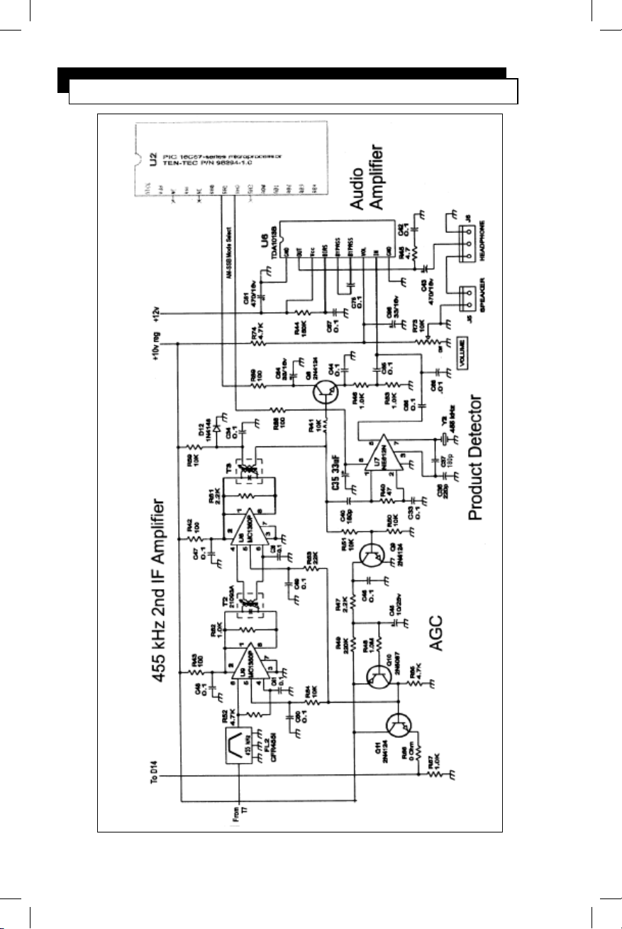
Phase 4.0 Schematic Details
1254 – Assembly - 36
Page 58
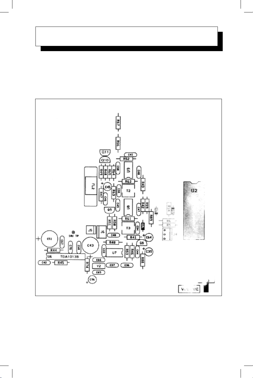
Phase 4.0 QUICK-REFERENCE SUMMARY
Before You Start: The f ollowing Quick Reference Summary of
the parts used in Phase 4.0 may be used first as a guid e to
gathering parts for this phase. lt is provided as an extra help in
double-checking correctness of parts values with brief notes on
the function of each part.
Phase 4.0
Audio Section, AGC, 455 kHz 2nd IF
After part 4A this phase is completed, we can test for audio
output and proper operat ion of the volume control. When this
phase is completed, the receiver also can detect a 455 kHz
signal such as from its 2nd mixer (Phase 5.0) in either AM or
SSB mode.
1254 – Assembly - 37
Page 59
Phase 4.0 QUICK-REFERENCE SUMMARY
Before You Start: The f ollowing Quick Reference Summary of
the parts used in Phase 4.0 may be used first as a guid e to
gathering parts for this phase. lt is provided as an extra help in
double-checking correctness of parts values with brief notes on
the function of each part.
C33
C34
C35
C36
C37
C38
C40
C41
C42
C43
C44
C45
C46
C47
C48
C49
C50
C51
C64
C65
C66
C67
C68
C75
C98
D12
T2
T3
U6
U7
U8
U9
Q8
Q9
Q10
Q11
R40
R41
R42
R43
R44
R45
0.1μF
0.1μF
33/16v el.
220 pF
180 pF
0.1μF
180 pF
0.1μF
0.1μF
470/16v el.
0.1μF
10/25v el.
0.1μF
0.1μF
0.1μF
0.1μF
0.1μF
470/16v el.
33/16v el.
0.1μF
0.1μF
0.1μF
.01μF
0.1μF
33/16v el.
1N4148
455 kHz coil
455 kHz coil
NTE1852
NE612N
MC1350P
MC1350P
2N4124
2N4124
2N5087
2N4124
47
10K
100
100
150K
4.7
Input bypass on U7
Bypass on output of T3
Supply bypass on U7
Oscillator cap on U7
“ “ “
Bypass on input of U8
Coupling cap into U7
Input bypass on U9
High frequency shunt on U8
Audio output coupling cap
RF bypass on Q8 base
AGC time cons tant cap
RF bypass on Q9
Supply bypass on U8
Supply bypass on U9
RF bypass on U8
RF bypass on U9
Supply bypass on U6 audio lC
Collector bypass on Q8
Output coupling from Q8 AM detector
Output coupling from product detector
Turn-on cap for U6
Bypass on input to U6
Interstage coupling on U6
Filter cap on volume control
Forward bias for AM detector
455 kHz lF amplifier
“ “
Audio amplifier
Product detector
IF amplifier
IF amplifier
AM detector
AGC rectifier
AGC integrator
AGC voltage follower
Input resistor to U7 product detector
Input resistor to AM detector
Supply to U8
Supply to U9
Power-on bias to U6
High frequency shunt on U6
1254 – Assembly - 38
Page 60
Phase 4.0 Quick Reference, cont.
Phase 4.0 Assembly Steps
Section 4A. Audio Amplifier Circuit
U6 is a self-contained audio amplifier SIP (single inline pin) IC,
using only a volume control and a very few resistors and
capacitors to complete a 1.5 wat t audio amplifier. We will
assemble this circuitry plus the speaker/headphone connections
now, then test their functioning, to confirm audio amplifier
performance before adding further stages to the receiver.
notched/ banded end is similar to other IC's used in the circuit.
Insert this end per the notched end on the silkscreen (nearest t he
space for C79) . Sol der carefully to avoid bridges, because shorts
can permanently damage U6!
jack cable. Align the locking end as outlined on the board, just as
you did when installing the jack for the enc oder cable.
the board, insert J5, the 2-pin header (just like the power switch
connector) for connecting the built-in speaker. Soldering is done
on the top (component) side. Align the locking end of J5 as
outlined on the top side. This header must be on the solder-side
for proper connection to the speaker when installed permanently.
Install the following electrolytic capacitors with correct polarity:
Install these supporting parts for U6:
making sure that all three solder tabs are squarely into the board
as far as they can go, to ensure a proper fit to the display board.
R46
R47
R48
R49
R50
R51
R52
R53
R59
R61
R62
R63
R64
R65
R66
R67
R73
R74
R88
R89
FL2
J5
J6
Y2
1.0K
2.2K
1.0 M
220K
10K
10K
4.7K
1.0K
10K
2.2K
1.0K
22K
10K
4.7K
0 ohm
1.0K
10K var
4.7K
100
100
CFR455I
2-pin header
3-pin header
455 kHz
AM detector emitter resistor
AGC discharging resistor
AGC time cons tant
AGC charging resistor
AGC rectifier pull-down
AGC input resistor
IF amp input load
AM detector emitter resistor
Forward bias for AM detector
IF amp output load, U8
IF amp output load, U9
AGC input resistor, U8
AGC input resistor, U9
AGC pull-down resistor
Front end AGC voltage divider
Front end AGC pull-down
Front panel volume
Volume control pull-up
Power feed for product detector
Power feed for AM detector
455 kHz filter
Internal speaker cable connector
Headphone jack cable connector
0scillator for product detector
1254 – Assembly - 39
Page 61
Phase 4.0 Assembly Steps
Section 4A. Audio Amplifier Circuit
U6 is a self-contained audio amplifier SIP (single inline pin) IC,
using only a volume control and a very few resistors and
capacitors to complete a 1.5 wat t audio amplifier. We will
assemble this circuitry plus the speaker/headphone connections
now, then test their functioning, to confirm audio amplifier
performance before adding further stages to the receiver.
4-1a. Examine amplifier IC U6, type TDA1013B and not ice its
notched/ banded end is similar to other IC's used in the circuit.
Insert this end per the notched end on the silkscreen (nearest t he
space for C79) . Sol der carefully to avoid bridges, because shorts
can permanently damage U6!
4-1b. Install audio IC U6, type NTE1852 per 4-1a.
4-2. Install J6, the three-pin connector for the headphone
jack cable. Align the locking end as outlined on the board, just as
you did when installing the jack for the enc oder cable.
4-3. READ before soldering: on the BOTTOM solder-side of
the board, insert J5, the 2-pin header (just like the power switch
connector) for connecting the built-in speaker. Soldering is done
on the top (component) side. Align the locking end of J5 as
outlined on the top side. This header must be on the solder-side
for proper connection to the speaker when installed permanently.
Install the following electrolytic capacitors with correct polarity:
4-4. Capacitor C96, 33 μF.
4-5a. Capacitor C43, 470 μF.
4-5b. Capacitor C51, also 470 μF.
Install these supporting parts for U6:
4-6. Resistor R45, 4.7 ohms (yellow-violet-gold).
4-7. Resistor R74, 4.7K (yellow-violet-red).
4-8. Resistor R44, 150K (brown-green-yellow)
4-9. Ceramic disc capacitor C42, 0.1 μF (marked 104).
4-10. Capacitor C67 , also 0.1 μF.
4-11. Capacitor C75, also 0.1 μF.
4-12. Install 10K potentiometer R73, the volume control,
making sure that all three solder tabs are squarely into the board
as far as they can go, to ensure a proper fit to the display board.
1254 – Assembly - 40
Page 62
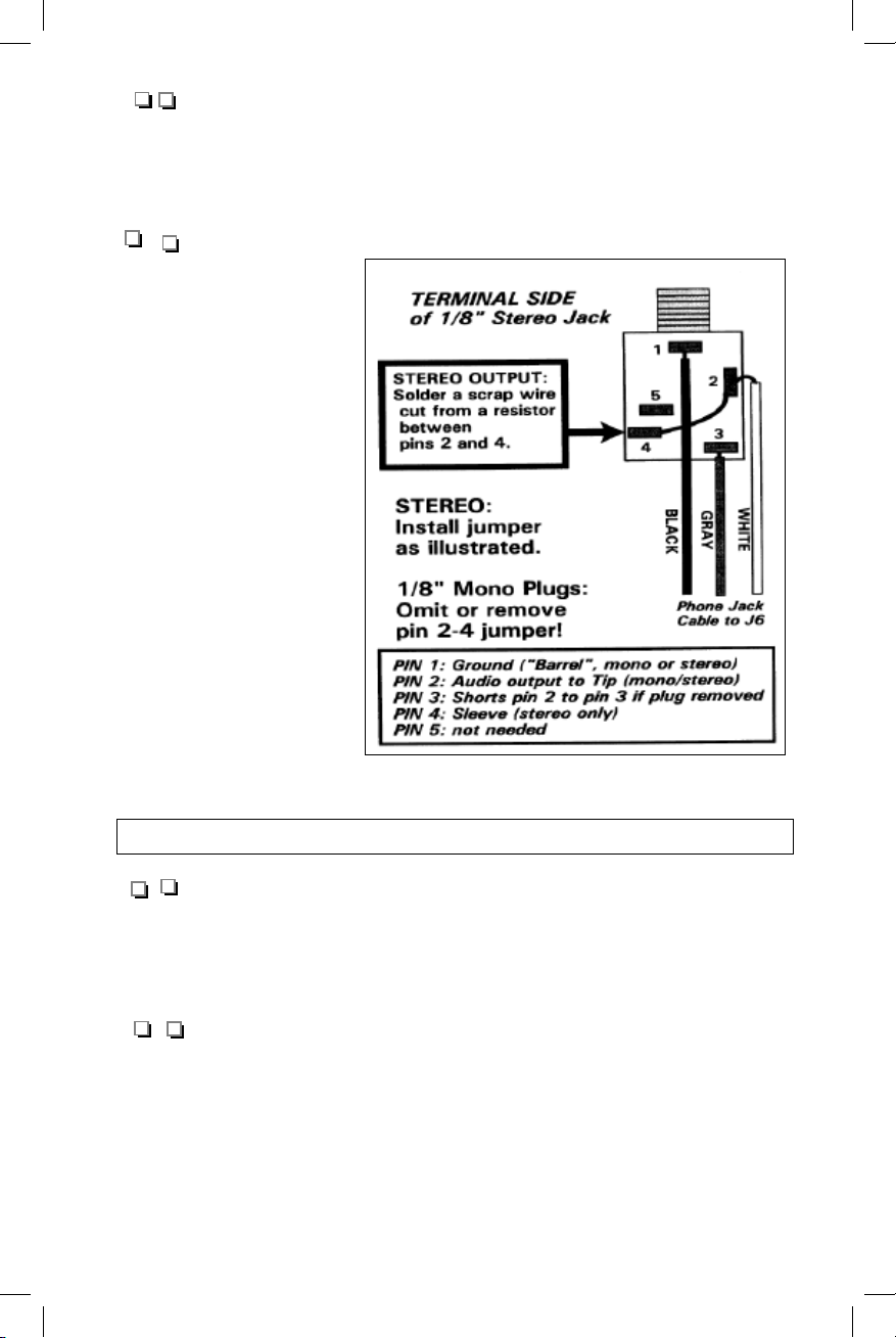
4-13. Strip 1/8" insulation from the ends of the black and
3.0 VCO tests. For this test, re-attaching the Display Board is
optional, but DO connect the power switch plug to J2. If you do
attach the display board, handle the volume control gently.
You should hear only a faint hiss which grows stronger with the
turning of the volume control. Hold a small screwdriver by its
shaft and touch the pad for C66 (not yet installed) which is
nearest audio IC U6. Your body contact with this input to U8
should produce a fairly loud hum (60 Hz AC house wiring).
correct your work before proceeding. The intentional AC hum
and the soft background hiss are the only sounds you should
hear. i.e., there must be no squeals or "putt-putt" motorboating
sounds.
During further assembly, handle the hoard carefully so that the
Volume Control leads are not bent hack and forth. The Clarifier
control will be mounted in Phase 5.0 and will require similar
carefulness.
Section 4B.
Product Detector and AM Detector Section
aligning the notched or dotted end as outlined on the board.
resonator, rectangular plastic case, 2 pins, marked 455BK).
Install the following 1/4-watt resistors:
white wires of the 2-conductor speaker cable. Solder the
stripped ends to the two terminals of t he 3" speaker supplied in
the kit. (White is "+", black is "-", but speaker polarity is not
critical in this application.)
4-14. Strip F
1/8" insulation
from all three
ends of the wires
of the 3-wire
headphone jack
cable. Solder the
stripped ends to
the 1/8" jack as
illustrated in
Figure 4.1.
Decide NOW if
this jack should
be wired for
stereo (normal) or
mono 1/8" plugs.
(A mono plug will
short out the jack
if wired for
stereo.)
igure 4.1: Headphone Jack Wiring Options
Progress Test 4A: Audio Amplifier
4-15. Connect the headphone jack cable assembly to J6.
This connection MUST be made regardless of whether you have
headphones or plan to tr y them out later. This is because the
stereo jack 's internal switching routes the amplifier output to the
J6 speaker connection with no plug inserted in the stereo jack.
4-16. Connect the r eceiver speaker to J5 on the solder-side
on the board and turn the volume control fully counter-clockwise.
1254 – Assembly - 41
Page 63
4-17. Reconnect the 15 volt DC supply to J1 as for the phase
3.0 VCO tests. For this test, re-attaching the Display Board is
optional, but DO connect the power switch plug to J2. If you do
attach the display board, handle the volume control gently.
4-18. Turn on DC power, then advance the volume control.
You should hear only a faint hiss which grows stronger with the
turning of the volume control. Hold a small screwdriver by its
shaft and touch the pad for C66 (not yet installed) which is
nearest audio IC U6. Your body contact with this input to U8
should produce a fairly loud hum (60 Hz AC house wiring).
4-19. If you do NOT obtain these test results, recheck and
correct your work before proceeding. The intentional AC hum
and the soft background hiss are the only sounds you should
hear. i.e., there must be no squeals or "putt-putt" motorboating
sounds.
During further assembly, handle the hoard carefully so that the
Volume Control leads are not bent hack and forth. The Clarifier
control will be mounted in Phase 5.0 and will require similar
carefulness.
Section 4B.
Product Detector and AM Detector Section
4-20. Install U7, the NE612AN or SA612AN 8-pin DIP IC,
aligning the notched or dotted end as outlined on the board.
4-21 . Install transistor Q8, NPN type 2N4124.
4-22. Install Y2, the 455 kHz oscillator device (ceramic
resonator, rectangular plastic case, 2 pins, marked 455BK).
Install the following 1/4-watt resistors:
4-23. Resistor R40, 47 ohm (yellow-violet-black).
4-24. Resistor R88, 100 ohms (brown-black-brown).
4-25. Resistor R89, also 100 ohms.
4-26. Resistor R46, 1K ( brown-black-red).
4-27. Resistor R53, also 1K.
4-28. Resistor R41, 10K ( brown-black-orange).
1254 – Assembly - 42
Page 64
Install the following ceramic disc capacitors:
Section 4C: IF Amplifier and AGC
the notched or dotted end as outlined on the board.
the notched or dotted end as outlined on the board.
band orientation as outlined on the board.
arrangement permits only one possible orientation. Simply ignore
the group of small circuit board holes covered by the filter case.
arrangement permits only one possible orientation. (While the
markings may vary, these transformers have 5 pins, 2 shield tabs
and are the only parts in the kit which will fit here.)
information in t he preceding step.
Install the following 1/4-watt resistors:
4-29. Capacitor C37, 150 pF (marked 151).
4-30. Capacitor C36, 220 pF (marked 221).
4-31. Capacitor C40, 180 pF (marked 181).
4-32. Capacitor C33, 0.1μF (marked 104).
4-33. Capacitor C44, also 0.1 μF.
4-34. Capacitor C46, also 0.1 μF.
4-35. Capacitor C65, also 0.1 μF.
4-36. Capacitor C66, also 0.1 μF.
4-37. Capacitor C68, 0.01 μF.
Install the following electrolytic capacitors with correct p olarity:
4-38. Capacitor C35, 33 μF.
4-39. Capacitor C64, 33 μF.
Progress Test 4B
PROCEDURE:
4-40. Reconnect the speaker Headphone jack cable
power switch plug, and DC power supply
4-41. Reconnect the Display Board as in Phase 2.0 testing.
4-42. Find the pad f or R41 (not yet installed) nearest to C40,
180 pF, very close to the headphone jack connector. This pad is
common to C40, the input coupling capacitor for U7.
4-43. Turn on DC power to the 1254 board. Adjust the
volume control to maximum. Set [MODE] t o SSB.
4-44. Touc h one end of a test lead to the pad for R41 nearest
C40. In SSB mode, you will hear a very slight increase in hiss
level. Place the other end of the test wire next to the 6-digit LED
display. You should hear low-level musical tones, which are
harmonics of the LED multiplexing circuit.
4-46. If you get the above-described result, turn off DC
power, disconnect all cables from the 1254 board, and proceed
to part 4C of Phase 4.0. If not, the first thing to do is to
review all parts installed in part 4B.
4-46-49. reserved
1254 – Assembly – 43
Page 65
Section 4C: IF Amplifier and AGC
4-50. Install U8, a MC1350P 8-pin DIP IC, being
the notched or dotted end as outlined on the board.
4-51. Install U9, a MC1350P 8-pin DIP IC, being
the notched or dotted end as outlined on the board.
4-52. Install transistor Q9, NPN type 2N4124.
4-53. Install transistor Q11, NPN type 2N4124.
4-54. Install transistor Q10, PNP t ype 2N5087.
4-55. Install diode D12, type 1N4148, with correct cathode
band orientation as outlined on the board.
4-56. Install the 455 kHz filter FL2 (labeled CFR455-I). Its pin
arrangement permits only one possible orientation. Simply ignore
the group of small circuit board holes covered by the filter case.
4-57. Install T2, a 455 kHz shielded transformer. Its pin
arrangement permits only one possible orientation. (While the
markings may vary, these transformers have 5 pins, 2 shield tabs
and are the only parts in the kit which will fit here.)
4-58. Install T3, a 455 kHz shielded transformer, per the
information in t he preceding step.
Install the following 1/4-watt resistors:
4-59. Resistor R66, "0 ohm" (one black band).
4-60. Resistor R42, 100 ohms (brown-black-brown).
4-61 . Resistor R43, also 100 ohms.
4-62. Resistor R62, 1K (brown-black-red).
4-63. Resistor R67, also 1K.
4-64. Resistor R47, 2.2K (red-red-red).
4-65. Resistor R61, also 2.2K.
4-66. Resistor R52, 4.7K (yellow-violet-red).
4-67. Resistor R65, also 4.7K.
4-68. Resistor R50, 10K ( brown-black-orange).
4-69. Resistor R51, also 10K.
4-70. Resistor R59, also 10K.
4-71 . Resistor R64, also 10K.
4-72. Resistor R63 , 22K (red-red-orange).
4-73. Resistor R49, 220K (red-red-yellow).
4-74. Resistor R48, 1 meg ohm (brown-black-green).
1254 – Assembly - 44
Page 66
Install these 0.1 μF disc capacitors (marked 104):
a problem in the circuitry associated with U7, the Product
Detector.
power, disconnect all cables from the 1254 board, set aside the
display board, and proceed to Phase 5.0! If not, please read on.
In this receiver project, it is impossible to say which is the most
important or critical phase. That's because EVERY circuit section
must perform correctly if this R e ceiver is to work as designed.
Hopefully, you found Phases 1.0 and 2.0 easy and fun: the
microprocessor and front panel display do their thing, and we
were off to a great start, thanks to digital technology.
The VCO/PLL circuitry in Phase 3.0 generates the RF tuning
signal ("LO") essential for mixing and converting signal from
your antenna, first to 45 MHz and then again to 455 kHz and
then again to intelligible audio.
Phase 4.0 is very important simply because it is the meeting
ground between your ear and all other "superheterodyne"
activity converging on it f rom the other circuit phases. If you did
not obtain the lest results explained for Phase 4.0, go over all
parts installed in this phase, using the double-check blocks for
the assembly steps, Then review the work using the Quick-
Reference list of Phase 4.0 parts at the beginning of this section.
If you know for sure that Phases 2.0, 3.0, and 4.0 work exactly
as explained in their Progress tests, then the upc oming work of
building up two mixer sections and RF input should make clearer
sense to you now.
4-75. Capacitor C34, 0.1 μF.
4-76. Capacitor C38, 0.1 μF.
4-77. Capacitor C41, 0.1 μF.
4-78. Capacitor C47, 0.1 μF.
4-79. Capacitor C48, 0.1 μF.
4-80. Capacitor C49, 0.1 μF.
4-81. Capacitor C50, 0.1 μF.
4-82. reserved
4-83. Install electrolytic capacitor C45, 10 μF with correct
( + ) polarity.
Final (4C) Phase 4.0 Progress Test
Some technicians may feel the only way to fully prove to all your
senses that all the circuitry built in Phase 4.0 is worki ng properly
is to see if a nearby 455 kHz signal can be detected. An RF
signal generator is the usual source for such a signal.
HOWEVER, this circuit is eng ineered to permit an extremely
SIMPLE test at this point!
If this section of the receiver has problems, no further amount of
work on the mixers or 45 MHz 1st IF can f ix problems in THIS
section.
PROCEDURE:
4-84. Reconnect: speaker headphone jack cable, power
switch plug DC power supply and the Display Board
4-85. Turn on DC power to the 1254 board. Adjust the
volume control to its midway point. If you can recall what you
heard in previous tests, you should notice a shar p increase in
background noise level introduced by adding the IF amplifier
section.
4-86. Touc h a meter test probe or even a screwdriver as you
did for the audio amplifier to the lead of R52 nearest Q1O. You
should note a sharp increase in background noise. This indicates
that the IF amplifiers are working correctly.
4-87. Switch the [MODE] button back and forth between AM
and SSB while still holding a probe at R52. In AM mode, you
should hear mainly a loud hum. In SSB mode, the sound
changes to a his s.
1254 – Assembly - 45
Page 67

4-88. If there is NO or very little sound in SSB mode, there is
a problem in the circuitry associated with U7, the Product
Detector.
4-89. If you get the above-described result, turn off DC
power, disconnect all cables from the 1254 board, set aside the
display board, and proceed to Phase 5.0! If not, please read on.
Building the T-KIT Model 1254 Receiver:
An “INTERMISSION”
In this receiver project, it is impossible to say which is the most
important or critical phase. That's because EVERY circuit section
must perform correctly if this R e ceiver is to work as designed.
Hopefully, you found Phases 1.0 and 2.0 easy and fun: the
microprocessor and front panel display do their thing, and we
were off to a great start, thanks to digital technology.
The VCO/PLL circuitry in Phase 3.0 generates the RF tuning
signal ("LO") essential for mixing and converting signal from
your antenna, first to 45 MHz and then again to 455 kHz and
then again to intelligible audio.
Phase 4.0 is very important simply because it is the meeting
ground between your ear and all other "superheterodyne"
activity converging on it f rom the other circuit phases. If you did
not obtain the lest results explained for Phase 4.0, go over all
parts installed in this phase, using the double-check blocks for
the assembly steps, Then review the work using the QuickReference list of Phase 4.0 parts at the beginning of this section.
If you know for sure that Phases 2.0, 3.0, and 4.0 work exactly
as explained in their Progress tests, then the upc oming work of
building up two mixer sections and RF input should make clearer
sense to you now.
1254 – Assembly - 46
Page 68

Phase 5.0 Schematic Details
This space is for your notes
1254 – Assembly – 47
Page 69
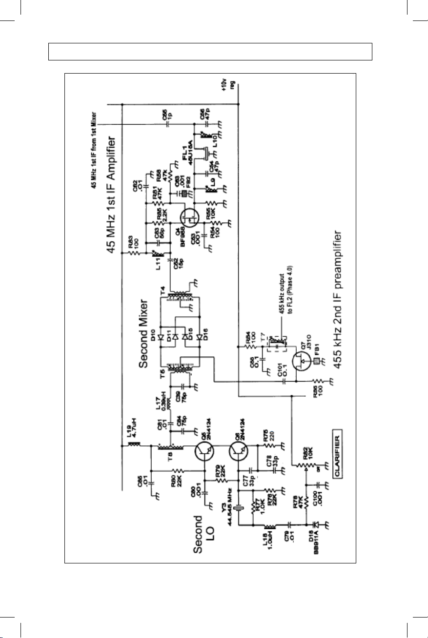
Phase 5.0 Schematic Details
1254 – Assembly - 48
Page 70
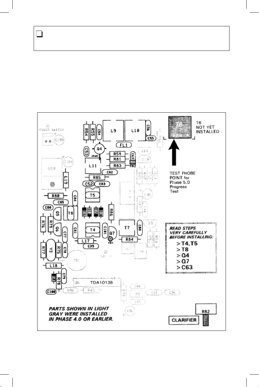
Phase 5.0
Phase 5.0 QUICK-REFERENCE INFORMATION
Second Mixer and 45 MHz First IF
The result of successful completion of this assembly phase will
be a receiver circuit capable of detect ing very strong nearby 45
MHz signals in either AM or SSB-CW mode. The Model 1254
has a built-in 45.000 MHz test signal capability.
1254 – Assembly – 49
Page 71
Phase 5.0 QUICK-REFERENCE INFORMATION
C39
C52
C53
C54
C55
C56
C63
C77
C78
C79
C80
C81
C82
C83
C84
C85
C88
C100
C101
D10
D11
D15
D16
D18
L9
L10
L11
L17
L18
L19
T4
T5
T7
T8
Q4
Q5
Q6
Q7
R54
R55
R58
R75
R76
R77
R78
R79
R80
R81
R82
R83
R84
R85
R86
FL1
Y3
FB1
FB2
75 pF
15 pF
.001μF
47 pF
1 μF
47 pF
.001μF
33 pF
33 pF
.01μF
.001μF
.01μF
.01μF
56 pF
75 pF
.01μF
0.1μF
.001μF
0.1μF
1N4148
1N4148
1N4148
1N4148
Factory Installed
0.25μH
0.25μH
0.12μH
0.39μH
1.0μH
4.7μH
trifilar balun
trifilar balun
455 kHz coil
bifilar bal un
BF988
2N4124
2N4124
J310
100
10K
47K
220
22K
1.0K
47K
22K
22K
47K
10K variable
100
100
2.2K
100
45U1A
44.545 MHz
ferrite bead
ferrite bead
Second LO output filter
Output coupling cap from Q4
Source bypass cap on Q4
Resonating cap on input of Q4
Input cap to FL1
Resonating cap on input to FL1
Gate-2 bypass on Q4
Second LO capacitor at Q6 base
" ""
Coupling cap to clarifier varicap
Base bypass on Q5
Second LO output coupling cap
Supply bypass for Q4
Output resonating cap for Q4
Second LO output filter
Supply bypass for Q5
Supply bypass for Q7
Bypass cap on clarifier control
Coupling capintoQ7
Second mixer diode
Second mixer diode
Second mixer diode
Second mixer diode
45 MHz filter
45 MHz filter
Mixer circuit
Mixer out
Y3 crystal tuning network
DC power RF choke
2nd mixer transformer
2nd mixer transformer
455 kHz output from mixer to 2nd IF
2nd LO output transformer
First IF amplifier
Second LO buffer
Second LO oscillator
455 kHz IF preamplifier
Source resistor for Q4
Gate load for Q4
Gate 2 bias for Q4
Second LO emitter resistor
Second LO bias
Crystal shunt resistor
Clarifier varactor bias
Second LO bias
Second LO bias
Gate 2 bias for Q4
Front panel Clarifier control
Supply feed for Q4
Supply feed for Q7
Drain load for Q4
Source resistor for Q7
45 MHz crystal filter
Second LO
put on gate lead of Q7
put on lead closest to "FB2" on board
1254 – Assembly - 50
Page 72
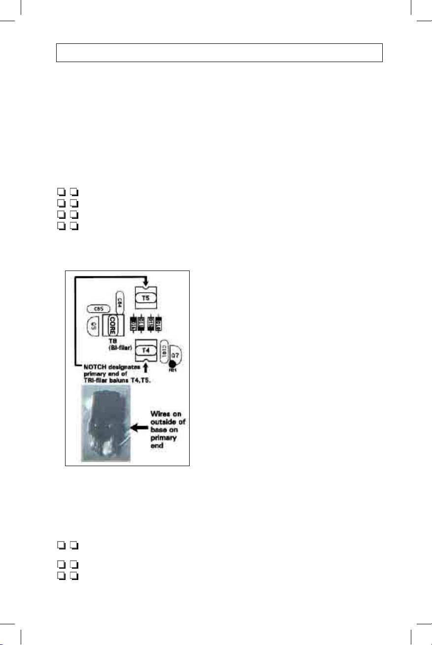
Phase 5.0 Assembly Steps
Install the following 1/4-watt resistors:
Install these ceramic disc capacitors:
Install these molded inductors:
installed in Phase 4.0).
is seated squarely on the hoard before soldering. (L11 is similar
to but smaller than coils L9 and L10).
Before You start: The preceding Quick Reference Summary of
the parts used in Phase 5.0 may be used first as a guide to
gathering parts for this phase. It is provided as an extr a help in
double-checking correctness of parts values with brief notes on
the function of each part.
Install mixer diodes D10-11, D1 5-16, type 1N4148, making sure
to align the black cathode bands exactly as outlined on the
board:
5-1. Diode D10, type 1N4148.
5-2. Diode D11, type 1N4148.
5-3. Diode D15, type 1N4148.
5-4. Diode D16, type 1N4148.
5-5. Select T4 and T5, the pre-
Figure 6.1
assembled trifilar (3 winding) balun
transformers, noting that they have
SIX pins. Notice carefully which
end of the plastic base has the two
yellow/gold primary wires coming
from the ferrite core over the base
to two pins. These two
transformers must be installed with
these primary ends furthest from
the mixer diodes as indicated by
the notches in the board silkscreen
and Figure 5.1.
5-6. Install trifilar balun
transformer T4 per 5-5.
5-7. Install trifilar balun
transformer T5 per 5-5.
5-8a. Examine tr ansformer T8,
the pre-assembled bifilar balun (4
pins) and its silkscreen outline on
the board. The ferrite core of T8
must be or iented as outlined on the
board and noted in Figure 5.1.
5-8b. Install transformer T8 per 5-8a.
5-9. Install transistor Q5, NPN type 2N4124.
5-10. Install transistor Q6, NPN type 2N4124.
1254 - Assembly – 51
Page 73
Install the following 1/4-watt resistors:
5-11. Resistor R54, 100 ohms (brown-black-brown).
5-12. Resistor R83, also 100 ohms.
5-13. Resistor R84, also 100 ohms.
5-14. Resistor R86, also 100 ohms.
5-15. Resistor R60, 220 ohms (red-red-brown).
5-16. Resistor R75, also 220 ohms.
5-17 Resistor R77, 1K (brown-black-red).
5-18. Resistor R85, 2.2K (red-red-red).
5-19. Resistor R55, 10K ( brown-black-orange).
5-20. Resistor R76, 22K (red-red-orange).
5-21. Resistor R79, also 22K.
5-22. Resistor R80, 22K.
5-23. Resistor R58, 47K (yellow-violet-orange).
5-24. Resistor R78, also 47K.
5-25. Resistor R81, also 47K.
Install these ceramic disc capacitors:
5-26. Capacitor C 55 , 1 pF.
5-27. Capacitor C52, 15 pF.
5-28. Capacitor C77,33 pF.
5-29. Capacitor C78, 33 pF.
5-30a. Capacitor C54, 47 pF.
5-30b. Capacitor C56, 47 pF.
5-31. Capacitor C83, 56 pF.
5-32. Capacitor C39, 75 pF.
5-33. Capacitor C84, 75 pF.
5-34. Capacitor C53, .001 μF (marked 102).
5-35. DO NOT install C63, .00l μF, until instructed.
5-36. Capacitor C80, also .001 μF.
Capacitor C100, also .001 μF.
Capacitor C79, .01 μF (marked 103).
Capacitor C81, also .01 μF.
Capacitor C82, also .01 μF.
Capacitor C85, also .01 μF.
Capacitor C88, 0.1 μF (marked 104).
Capacitor C101, also 0.1 μF.
Install these molded inductors:
5-44. Coil L17, 0.39 μH (orange-white-silver-gold).
5-45. Coil L18, 1.0 μH {brown-black-gold-gold).
5-46. Coil L19, 4.7 μH (yellow-violet-
5-47. Install 455 kHz transformer T7 (identical to T2 and T3
installed in Phase 4.0).
5-48. Install the unshielded slug-tuned coil L11, being sure it
is seated squarely on the hoard before soldering. (L11 is similar
to but smaller than coils L9 and L10).
1254 - Assembly - 52
gold-gold).
Page 74
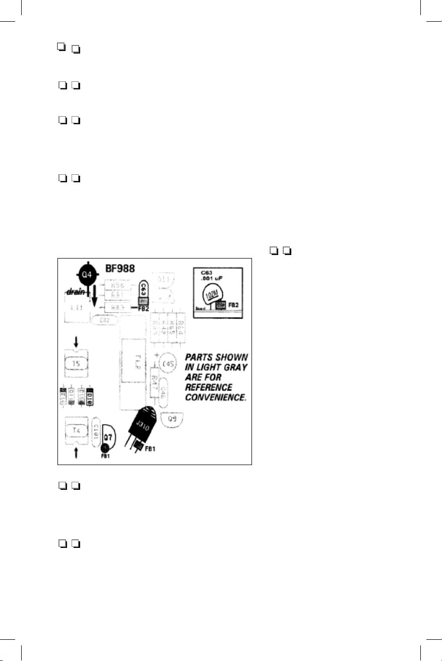
5-49. Install the unshielded slug-tuned coil L9, being sure it is
looks like a small crystal but with three leads.
44.545 MHz, then install Y3 in the normal manner.
Before soldering, make sure the control is mounted squarely
against the board, to assure proper mating to the display board.
several times for previous Progress Tests, you should be satisfied
that the DC on-off power switch is wired correctly. This means
one red wire to the center terminal, and the other to the bottom
when the display board faces you correctly.
REMOVE the unused (UPPER) lug of the power switch. Doing so
will prevent the unneeded lug from pushing into the nearest parts
on the main board when mounted permanently.
Phase 5.0 Progress Test
At this point in the project, we have a complete signal path from
the input of the 45 MHz IF out to the speaker. We cannot tune
the receiver because there is no mixer stage Yet. However, we
can tune the synthesizer output down to 45.000 MHz to
generate a built-in test signal.
Volume and Clar ifer controls and set them aside. Reconnect the
display board, being gentle with the controls as the shafts are
passed through their holes.
the power switch and adjust the volume control for moderate
background noise. Set the Mode switch to SSB.
LEFT pad in the row of three pads within the outline for trans-
former T6. This has t he effect of connecting a short "antenna"
directly to the input of the 45 MHz 1st IF through C55.
seated squarely on the board before soldering.
5-50. Install the unshielded slug-tuned coil L10, being sure it
is seated squarely on the board before soldering.
5-51. Slip the smallest shield c an over L11 and the two larger
shield cans over L9 and L10. These cans fit snugly over the
inductors. Make sure all three are seated squarely on the board,
then solder all six mounting tabs.
5-52. Diode D18, Is factory installed.
Correct installation of Q4, Q7 and C63
require careful attention to the following directions
while referring to Figure 5.2.
Figure 5.2: Q4, Q7, C63
type BF988, noting
that the tab for the
drain is longer than the
other three. It must be
aligned as illustrated in
Figure 5.2. If you live
in a dry climate,
discharge static
electricity from your
hands and tools before
handling Q4. The
imprinted side of Q4
faces up. Bend all four
tabs straight down
from the transistor
body, insert, then
solder all four
connections.
5-53. Examine Q 4,
5-54. Capacitor C63, .001 μF (marked 102), requires a ferrite
bead on the lead nearest the "FB2" label on the board. Simply
slip the bead on the lead, seat the capacitor as far as both leads
can go down, and solder both leads in the normal way.
5-55. JFET transistor of, type J310, is installed in the
normal manner but with a ferrite bead slipped over the gate
(grounded) lead as illustrated in Figure 5.2.
1254 - Assembly – 53
Page 75
5-56. Install FL1, the 45 MHz crystal filter (45U1A), which
looks like a small crystal but with three leads.
5-57. Slip a base insulator over the leads of crystal Y3.
44.545 MHz, then install Y3 in the normal manner.
5-58. Install 10K potentiometer R82, the Clarifier control.
Before soldering, make sure the control is mounted squarely
against the board, to assure proper mating to the display board.
5-59a. Now that you have connected the Display Board
several times for previous Progress Tests, you should be satisfied
that the DC on-off power switch is wired correctly. This means
one red wire to the center terminal, and the other to the bottom
when the display board faces you correctly.
5-59b. If all is well per 5-59a, use your cutter or nipper to
REMOVE the unused (UPPER) lug of the power switch. Doing so
will prevent the unneeded lug from pushing into the nearest parts
on the main board when mounted permanently.
Phase 5.0 Progress Test
At this point in the project, we have a complete signal path from
the input of the 45 MHz IF out to the speaker. We cannot tune
the receiver because there is no mixer stage Yet. However, we
can tune the synthesizer output down to 45.000 MHz to
generate a built-in test signal.
5-60. Remove any m ounting nuts and washers from the
Volume and Clar ifer controls and set them aside. Reconnect the
display board, being gentle with the controls as the shafts are
passed through their holes.
5-61. Reconnect these cables: Encoder Headphone jack
Internal Speaker DC power switch
5-62. Reconnect the 15VDC power supply to J1. Turn on
the power switch and adjust the volume control for moderate
background noise. Set the Mode switch to SSB.
5-63. Touc h the probe of one of your voltmeter leads to the
LEFT pad in the row of three pads within the outline for transformer T6. This has t he effect of connecting a short "antenna"
directly to the input of the 45 MHz 1st IF through C55.
1254 – Assembly - 54
Page 76
5-64. Touc hing the pr obe as explained above should cause a
Phase 6.0 Schematic Details
very dis tinct increase in background noise level. Adjust coils L9
and L10 for maximum noise level. If you can do this, you have
confirmed that there is a functioning signal path from C55
through all the circuitry you installed in Phase 4.0 and 5.0 to the
audio amplifier. (If there is any local noise or static which would
cause interference in any other radio, you will hear that too! for
example: lightning, noise from appliances, power lines, etc.)
5-65. Lay your test lead wire so that it is near the LED
frequency display. With the probe touching the left T6 pad, you
should hear a strong music-like blend of tones which are
harmonics of the multiplexing signals which illuminate the
display, as explained in the Circuit Description" Rotating the
clarifier control should change the pitch of the tone(s) you are
hearing. Rotating the tuning control will cause audible clicks.
5-66. Press the [SPEED] button for FAST (100 kHz) tuning
steps as indicated by the LED below the switch button. Tune
down until the display reads 0.000.0. The synthesizer is now
programmed to a frequency of 45.000 MHz, and the output level
is strong enough t o be picked up by the Q4 circuitry. (NOTE: the
synthesizer cannot be tuned below the 100 kHz limit using 2.5 or
5 kHz steps.) The 45.000 MHz LO signal should be very strong,
and you can adjust its pitch with the clar ifier control.
If you have observed the test results explained here, you can
proceed with confidence to the RF input and First Mixer sections
which will combine the signals from an antenna with the LO
output of the 45- 75 MHz frequency synthesizer, feeding the 45
MHz IF, resulting in a completed receiver!
5-67. Disconnect the DC supply, disconnect all cables and
set aside the display board.
Phase 6.0 Assembly
begins on page 56 ►
1254 - Assembly - 55
Page 77
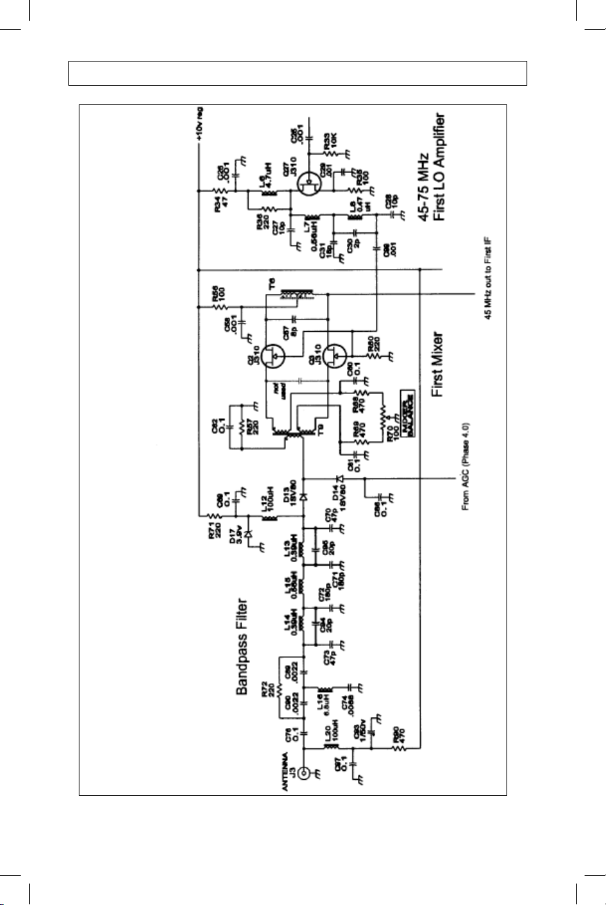
Phase 6.0 Schematic Details
1254 – Assembly - 56
Page 78
Phase 6.0 QUICK-REFERENCE INFORMATION
For your convenience, the complete hoard drawing for Phase 6.0
is presented on Page 62 after we finish the two shielded sections
for which separat e drawings are provided.
Before You Start: The preceding Quick Reference Summary of
the parts used in Phase 6.0 may be used first as a guide to
gathering parts for this phase. It is provided as an extr a help in
double-checking correctness of parts values with brief notes on
the function of each part.
6A. Shielded RF Input Bandpass Filter
This circuitry will be enclosed within a shield just like the VCO's.
Therefore, careful attention to correct parts selection is especially
important. Figure 6.1 is provided for your convenience.
Figure 6.1
Phase
6.0
RF Input Circuit and First Mixer
C25
C26
C27
C28
C29
C30
C31
C57
C58
C60
C61
C62
C69
C70
C71
C72
C73
C74
C76
C86
C89
C90
C93
C94
C95
C97
C99
D13
D14
D17
L6
L7
L8
L12
L13
L14
L15
L16
L20
T6
T9
Q2
Q3
Q27
R33
R34
R35
R36
R56
R57
R60
R68
R69
R70
R71
R72
R90
.001μF
.001μF
10 pF
10 pF
.001μF
2 pF
18 pF
8 pF
.001μF
0.1μF
0.1μF
0.1μF
0.1μF
47 pF
180 pF
180 pF
47 pF
.0068μF film
0.1μF
0.1μF
.0022μF film
.0022μF film
1/50v el.
20 pF
20 pF
0.1μF
.001μF.
BA479G
BA479G
3.9V zener
4.7μH
0.56μH
0.47μH
100 μH
0.39μH
0.39μH
0.56μH
6.8μH
100μH
1μH w/CT
trifilar balun
J310
J310
J310
10K
47
100
220
100
220
220
470
470
100 trimmer
220
220
470
Coupling cap into Q27
Supply bypass for Q27
1st LO output filter
" ""
Source bypass on Q27
1st LO output filter
“ “ “
Resonating cap on mixer T6
Supply bypass on first mixer
RF bypass on mixer transformer
" " ""
" " ""
" " ""
RF Input lowpass filter
" ""
" ""
RF Input lowpass filter
AM broadcast notch
Antenna input coupling cap
RF bypass on AGC diode Q14
AM broadcast input filter
“ “ “
Supply bypass for active antenna DC
Antenna input lowpass filter
“ “ “ “
Supply bypass for antenna DC
First LO output coupling cap
Front end AGC series diode
Front end AGC shunt diode
Front end AGC bias
LO amplifier DC supply choke
LO output lowpass network
“ “
Front-end AGC RFC
RF input bandpass filter
"" "
"" "
AM broadcast notch with C74
RFC for active antenna DC supply
First mixer input
First mixer output
First Mixer with Q3
First Mixer with Q2
First LO output amplifier
Gate pull-down tor Q27
Supply resistor tor Q27
Source resistor tor Q27
Drain load tor Q27
Supply resistor for first mixer
Front end AGC return
Output load for first LO
First mixer balance
First mixer balance
Mixer balance adjustment
Front end AGC forward bias
AM broadcast attenuator
Source resistor fol antenna DC
“
Page 79
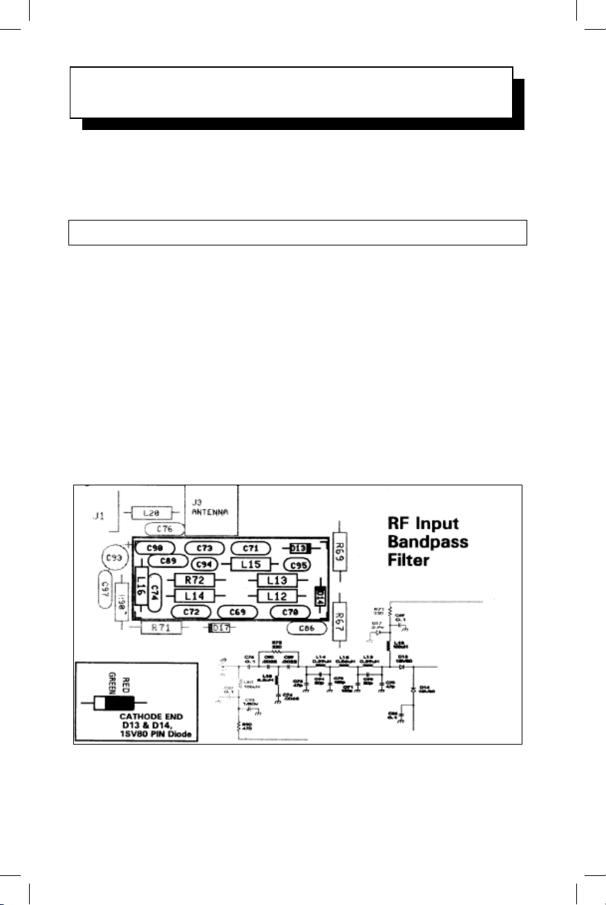
Phase
6.0
RF Input Circuit and First Mixer
For your convenience, the complete hoard drawing for Phase 6.0
is presented on Page 62 after we finish the two shielded sections
for which separat e drawings are provided.
Phase 6.0 Assembly
Before You Start: The preceding Quick Reference Summary of
the parts used in Phase 6.0 may be used first as a guide to
gathering parts for this phase. It is provided as an extr a help in
double-checking correctness of parts values with brief notes on
the function of each part.
6A. Shielded RF Input Bandpass Filter
This circuitry will be enclosed within a shield just like the VCO's.
Therefore, careful attention to correct parts selection is especially
important. Figure 6.1 is provided for your convenience.
Figure 6.1
1254 – Assembly - 58
Page 80
Install these mylar film capacitors:
68. Shielded First Mixer Section
This circuitry will be enclosed within a shield just like the VCO's.
Therefore, careful attention to correct parts selection is especially
important. Figure 6.2 is provided for your convenience. The
complete Phase 6.0 parts placement drawing is on page 58.
Figure 6.2
Be careful not to damage the mounting legs when inserting.
Correctly installed, it is normal to have some space between the
the board and the base of the trimmer.
but larger than the 455 kHz transformers installed in Phase 4.0.
with SIX pins, (identical to T4 and T5 installed in Phase 5.0).
Notice carefully which end of the plastic base has the two
copper-colored primary wires coming from the ferrite core over
the base to two pins . This transformer must be installed with
this primary end nearest trimmer R70 as indicated by the notches
in the board silkscreen and Figure 6.2.
6-1. Capacitor C89, .0022 μF (marked 222).
6-2. Capacitor C90, also .0022 μF.
6-3. Capacitor C74, .0068 μF (marked 682).
Install these ceramic disc capacitors:
6-4. Capacitor C94, 20 pF.
6-5. Capacitor C95, 20 pF.
6-6. Capacitor C70, 47 pF.
6-7 Capacitor C73, 47 pF.
6-8. Capacitor C71, 180 pF (marked 181).
6-9. Capacitor C72, also 180 pF.
6-10. Capacitor C69, 0.1 μF (marked 104).
6-11. Install resistor R72 220 ohms (red-red-brown).
6-12. Carefully identify PIN diode D13, type BA479G (Black
body, red cathode band, middle green band) and install
with correct cathode polarity.
6-13. Install diode D14, also type BA479G per 6-12.
Install the following molded inductors:
6-14. L13, 0.39 μH (orange-white-silver-gold).
6-15. L14, also 0.39 μH.
6-16. L15, 0.56 μH (green-blue-silver-gold)
6-17 L16, 6.8 μH (blue-gray-gold-gold).
6-18. L12, 100 μH (brown-black-brown-gold).
6-19. After carefully double-checking the parts just installed
for correct values, install a shield enclosure, soldering all four
mounting tabs. It is not necessary to bend these tabs before
soldering. No top cover is used on this shield or on the 1st
Mixer section to be built next.
REMINDER: Handle the board carefully to prevent damage to the
mounting lugs of the Volume and Clarifier controls.
1254 - Assembly - 59
Page 81
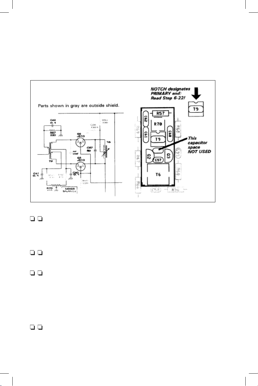
68. Shielded First Mixer Section
This circuitry will be enclosed within a shield just like the VCO's.
Therefore, careful attention to correct parts selection is especially
important. Figure 6.2 is provided for your convenience. The
complete Phase 6.0 parts placement drawing is on page 58.
Figure 6.2
6-20. Install the 100 ohm trimmer potentiometer R70.
Be careful not to damage the mounting legs when inserting.
Correctly installed, it is normal to have some space between the
the board and the base of the trimmer.
6-21 . Install the shielded adjustable coil T6, similar in style
but larger than the 455 kHz transformers installed in Phase 4.0.
6-22. Install T9, a pre-ass embled trifilar balun transformer,
with SIX pins, (identical to T4 and T5 installed in Phase 5.0).
Notice carefully which end of the plastic base has the two
copper-colored primary wires coming from the ferrite core over
the base to two pins . This transformer must be installed with
this primary end nearest trimmer R70 as indicated by the notches
in the board silkscreen and Figure 6.2.
6-23. Install resistor R57, 220 ohms (red-red-brown).
1254 - Assembly - 60
Page 82
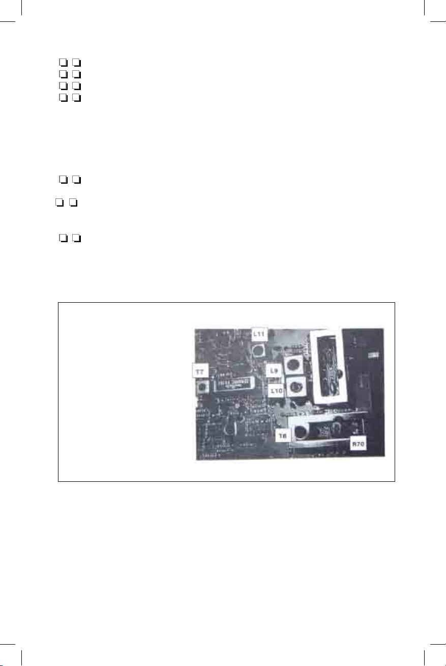
Install the following ceramic disc capacitors:
6C. Components Outside
Figure 6.3
Install these 1/4-watt resistors:
Install these ceramic disc capacitors:
6-24. Capacitor C57, 8pF.
6-25. Capacitor C60, 0.1 μF (marked 104).
6-26. Capacitor C61, also 0.1 μF.
6-27. Capacitor C62, also 0.1 μF.
NOTE: Ther e is an unlabeled outlined for a capacitor next to C57
which would serve as a shunt across trifilar balun T9. However,
further engineering determined no capacitor is needed here, and
this is the-only such "vacancy" on the entire 1254 circuit board.
6-28. Install transistor Q2, JFET type J310, being sure to
orient the flat side as outlined.
6-29. Install transistor Q3, JFET type J 310, being sure to
orient the flat side as outlined
6-30. After carefully double-checking the parts just installed
for correct values, install a shield enclosure, soldering all four
mounting tabs. No top cover is used here.
Figure 6.2b
Alignment Preview
After Phase 6.0 is finished
and panel/chassis sections
installed, the Model 1254
is aligned simply by adjusting
these coils for peak signal
strength.
T6
T9
L10
T7
R70 is adjusted for
minimum background
noise at 300 kHz
1254 - Assembly - 61
Page 83
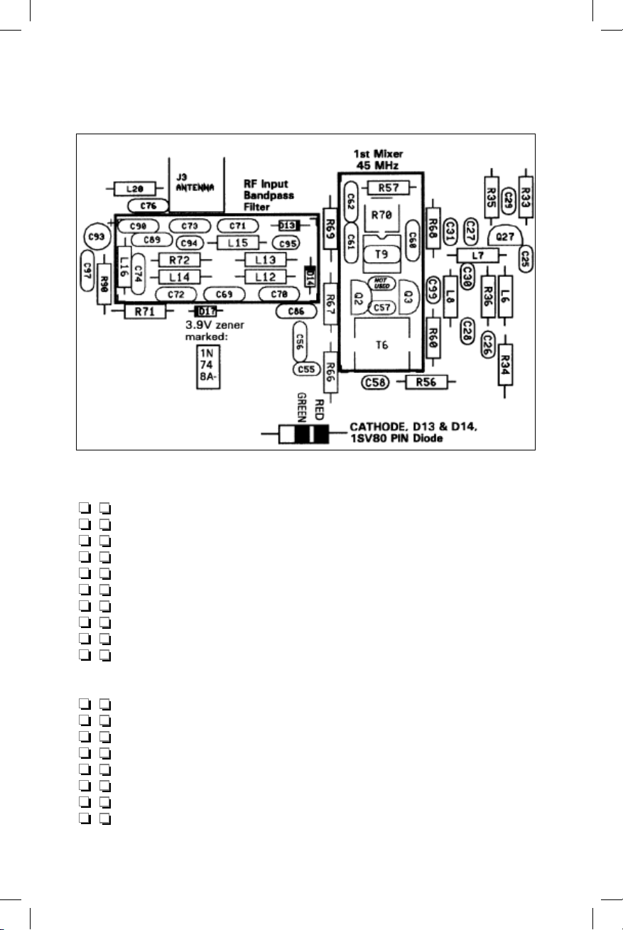
6C. Components Outside
the Shielded Enclosures
Figure 6.3
Install these 1/4-watt resistors:
6-31. Resistor R34, 47 ohms (yellow-violet-black).
6-32. Resistor R35, 100 ohms (brown-black-brown).
6-33. Resistor R56, also 100 ohms.
6-34a. Resistor R36, 220 ohms (red-red-brown).
6-35. Resistor R71, also 220 ohms.
6-36. Resistor R68, 470 ohms (yellow-violet-brown).
6-37. Resistor R69, also 470 ohms.
6-38. Resistor R90, also 470 ohms.
6-39. Resistor R33, 10K (brown-black-orange).
Install these ceramic disc capacitors:
6-40. Capacitor C 30 , 2 pF.
6-41 . Capacitor C27, 10 pF.
6-42. Capacitor C28, 10 pF.
6-43. Capacitor C31, 18 pF.
6-44. Capacitor C25, .001 μF (marked 102).
6-45. Capacitor C26, also .001 μF.
6-46. Capacitor C29, also .001 μF.
6-47. Capacitor C58, also .001 μF.
1254 - Assembly - 62
Page 84
Ceramic disc capacitors, cont .
Final Assembly of Model 1254 Receiver
The completed Model 1254 Receiver can indeed be fully aligned
and tested NOW while still in "board form" before adding the
front panel and other hardware. Doing it this way seems
advisable ONLY if you have nagging doubts about a previous
circuit phase test and if you feel t he added har dware might
interfere with testing and possible parts replacement in confined
areas, especially near the front panel. However, if all previous
"Progress Tests" have worked well for you, you'll probably prefer
the satisfaction of doing the final checkout of a mostly-
assembled receiver, nearly ready to use -- for real!
If you prefer the conservative approach, perform Step 7-1a, then
perform all Final Alignment instructions in Part 7B. If all goes
well, return to step 7-1b to continue Final Assembly.
both the Volume and Clarifier controls to the Display Board with
the flat washers and mounting nuts supplied. Reconnect the
Power Switch and Encoder Cables.
7A: Front Panel and Chassis Installation
Suggestion: Read over all the following panel assembly directions
and see Figures 7.1 and 7.2 BEFORE starting. Also, you may
wish to wrap the outer sides of the font panel with masking
tape to prevent scuffing during further assembly.
and notice the 5 support posts for the mounting screws.
Mounting the panel to the display board may be easier if you first
"exercise" the 5 mounting holes in the posts simply by screwing
in and removing a #4 self-tapping ("sheet metal") screw. Do this
for each post .
board controls.
6-48. Capacitor C99, also .00l μF.
6-49. Capacitor C76, 0.1 μF (marked 104).
6-50. Capacitor C86, also 0.1 μF.
6-51. Capacitor C97, also 0.1 μF.
6-52. Install electrolytic capacitor C93, 1 μF with correct
polarity.
6-53. Install 3.9v zener diode D17 , type 1N748A. (Review
p. 62 if you have any question about identifying this diode.)
Install these molded inductors:
6-54. Coil L8, 0.47 μH (yellow-violet-silver-gold.)
6-55. Coil L7, 0.56 μH (green-blue-silver-gold.)
6-56. Coil L6, 4.7 μH (yellow-violet-gold-gold.)
6-57. Coil L20*, 100 μH (brown-black-brown-gold.)
*Note: L20 supplies DC voltage to the antenna jack to power a remote
active antenna circuit. It is not essential to the receiver circuit and may be
omitted.
6-58. Install transistor Q27, JFET type J310.
Please Read First
6-59. The RCA-type antenna jack J3 will be subjected to
considerable stress over the life of the receiver as different
connectors or adapters are used. Therefore, we recommend that
its installation be as solid as possible, which means t hat it must
be flush against the board with strong solder connections.
6-60. Install antenna jack J3 per 6-59. Make sure that solder
flows generously around the pins and solder pads.
6-61. Your 1254 Receiver is "built," now needing only the
adjustment of a few coils and the addition of cabinet hardware to
make it useful and attractive. This remaining work should be
pure fun, so we encourage you to take your time and enjoy the
results.
1254 - Assembly - 63
Page 85
Phase 7.0
Final Assembly of Model 1254 Receiver
ALIGNMENT SUGGESTION:
The completed Model 1254 Receiver can indeed be fully aligned
and tested NOW while still in "board form" before adding the
front panel and other hardware. Doing it this way seems
advisable ONLY if you have nagging doubts about a previous
circuit phase test and if you feel t he added har dware might
interfere with testing and possible parts replacement in confined
areas, especially near the front panel. However, if all previous
"Progress Tests" have worked well for you, you'll probably prefer
the satisfaction of doing the final checkout of a mostlyassembled receiver, nearly ready to use -- for real!
If you prefer the conservative approach, perform Step 7-1a, then
perform all Final Alignment instructions in Part 7B. If all goes
well, return to step 7-1b to continue Final Assembly.
7-1a. Plug the Display Board into the Main Board and secure
both the Volume and Clarifier controls to the Display Board with
the flat washers and mounting nuts supplied. Reconnect the
Power Switch and Encoder Cables.
7A: Front Panel and Chassis Installation
Suggestion: Read over all the following panel assembly directions
and see Figures 7.1 and 7.2 BEFORE starting. Also, you may
wish to wrap the outer sides of the font panel with masking
tape to prevent scuffing during further assembly.
7-1b. Lay the front panel face down on a protective cloth,
and notice the 5 support posts for the mounting screws.
Mounting the panel to the display board may be easier if you first
"exercise" the 5 mounting holes in the posts simply by screwing
in and removing a #4 self-tapping ("sheet metal") screw. Do this
for each post .
7-2. Remove any knobs you may have attached to the display
board controls.
7-3. Check all control and switch nuts for normal tightness.
1254 - Assembly - 64
Page 86
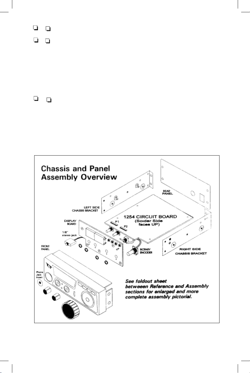
7-4. Make sur e none of the LED wires have been bent.
you are waiting, we again encourage you to read the remaining
instructions and study the drawings. Glue is also used to secure
the TEN-TEC logo and t o mount the speaker to its aluminum
support shelf. You may wish to study those instructions and
take care of those chores now.
panel hole created by the special insert. The body of the jack
should be parallel to the top and bottom of the front panel.
Tighten the jack's mounting nut very carefully to avoid
scratching surrounding areas.
switches on the Dis play Board.
Table 7.1: SMALL HARDWABE PREVIEW
# Description P/N Function
8 #4-40 1/4” screw,
4 #4-40 1/4” screw,
8 #4-40 3/16”
4 #4 split
5 #4 self-threading
NOTE: a #4-40 screw, phillips, #4 i nternal tooth lock washer, and #4-40 hex nut were
included in the Semiconductor package and should have been used already to mount Voltage
Regulator U10.
handy, fit the panel to the display board, gently guiding the
SPEED LED as needed. W hile holding everything together, ins tall
the screw in the center mounting hole near t he Clarifier control.
four mounting holes in whatever order is most convenient.
7-5. Set the display lens in position, making sure that the
"AM-SSB" lettering is facing correctly. The lens is locked into
place by carefully melting with your soldering tip the 6 molded
posts inside the panel along t he sides and bottom of the lens.
(If you are reluctant to do it this Way, you have the option of
securing the lens to the panel with very small drops of contact
cement at the edges.) Wipe the inside of the lens clean of any
fingerprints.
7-6a. Glue the front panel headphone jack insert in place.
This is a custom-molded washer-like plastic part. (The large hole
in the front panel is designed to accept connector s of various
types using the proper insert.) Use just a drop or two of any
fast-drying glue such as contact cement dried properly on both
surfaces. Do not use "superglue" here -- there is too much risk
of damaging the front panel surface.
Figure 7.1
1254 – Assembly - 65
Page 87
7-6b. Let the glue for the jack insert dry as needed. While
you are waiting, we again encourage you to read the remaining
instructions and study the drawings. Glue is also used to secure
the TEN-TEC logo and t o mount the speaker to its aluminum
support shelf. You may wish to study those instructions and
take care of those chores now.
7-7. Mount the 1/8" stereo jack (cable unplugged) to the
panel hole created by the special insert. The body of the jack
should be parallel to the top and bottom of the front panel.
Tighten the jack's mounting nut very carefully to avoid
scratching surrounding areas.
7-8. Press the four "key cap" buttons onto the button
switches on the Dis play Board.
Table 7.1: SMALL HARDWABE PREVIEW
# Description P/N Function
8 #4-40 1/4” screw,
phillips [zinc]
4 #4-40 1/4” screw,
phillips, [black]
8 #4-40 3/16”
undercut (“counter-
sink”) screw
4 #4 split
lockwasher
5 #4 self-threading
(“sheet metal”)
screw
NOTE: a #4-40 screw, phillips, #4 i nternal tooth lock washer, and #4-40 hex nut were
included in the Semiconductor package and should have been used already to mount Voltage
Regulator U10.
60001 Circuit board mounting (4)
Mount rear panel ends
of chassis brackets (4)
60032 Mount top and bottom shells to chassis
brackets in final assembly
60080 Mount front panel to chassis ends (4)
Mount Speaker/Battery shelf to chassis (4)
51058 Use between #60001 screws and top of
board to mount circuit board.
65009 Mount Display Board to front panel
7-9. Keeping a #4 self-threading screw and small screwdriver
handy, fit the panel to the display board, gently guiding the
SPEED LED as needed. W hile holding everything together, ins tall
the screw in the center mounting hole near t he Clarifier control.
7-10. Install additional #4 self-threading screws in the other
four mounting holes in whatever order is most convenient.
1254 – Assembly - 66
Page 88
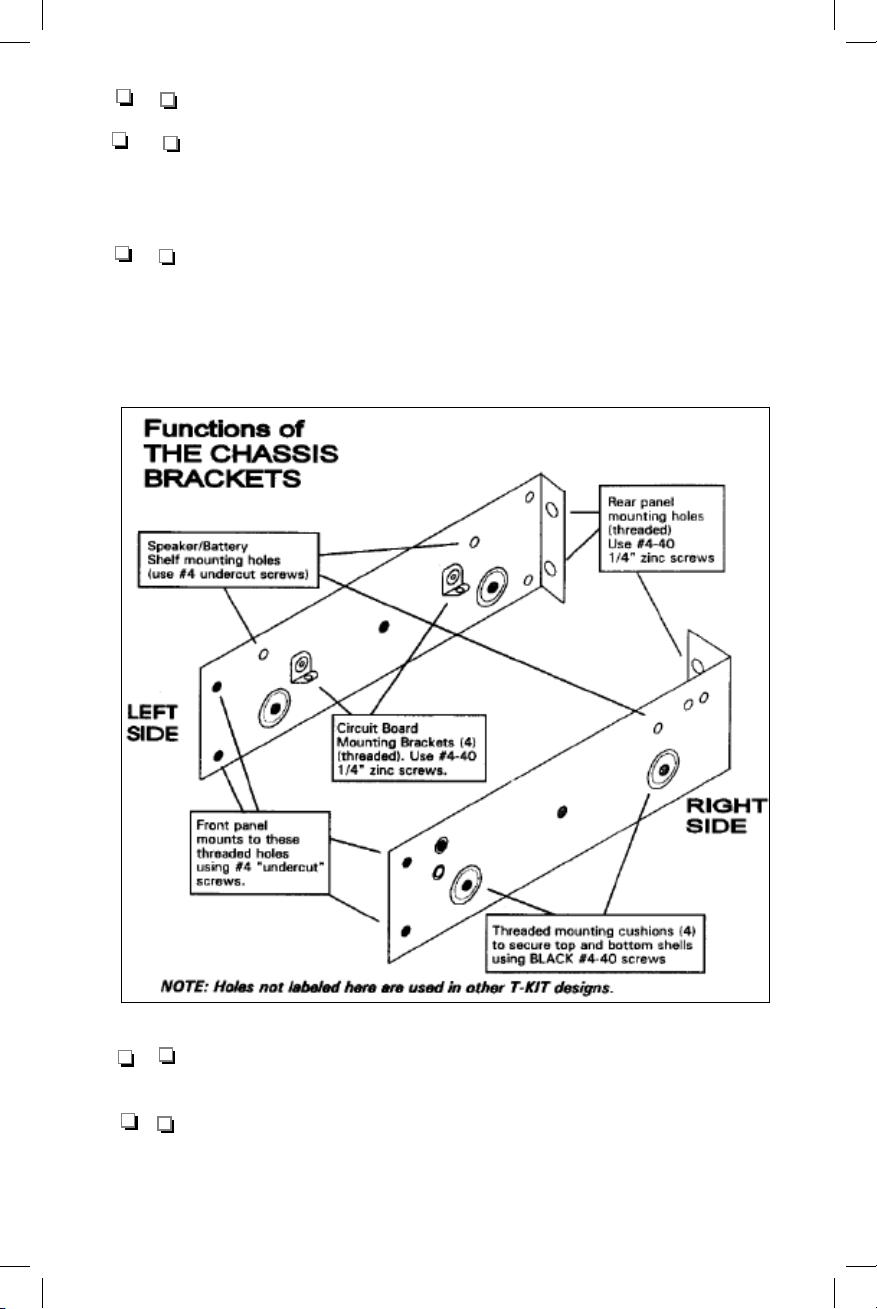
7-11. Tighten all 5 Display Board mounting screws.
1/4" #4-40 screws and two #4 lock washers.
#4-40 undercut screws.
panels, using four 1/4" #4-40 screws.
of the board.
mounting legs on the bottom side, leaving them straight (i.e.,
there is no need to bend them). Use a minimal amount of solder
to get good connections to the groundplane.
of the board and solder the mounting legs as for VCO-1.
if the primary use of your receiver will be vehicle-mounted.
To assure maximum VCO stability, you can do exactly what we do in factory -
built equipment. Use a hot-melt glue gun to flow glue liberally around the
outside of each VCO coil. it's OK if glue also covers some of the nearby parts.
The idea is to increase the body weight and mass of the coil itself , further
securing i t to the board. Be sure not to get any glue inside the coil, which would
interfere with any further adjustment. Again, this procedure is NOT NECESSARY
for ordinary receiver operation.
accessible through the hole. Solder the cover to the main shield.
Soldering each of the 4 corners is sufficient.
that the Power Switch and Encoder cables are plugged in.
your DC voltmeter to the VCO test point and ground as you did
in Phase 2.0.
7-12. Install the the Volume and Clarifier control knobs.
Before tightening the s etscrews, line up the index stripes
correctly in reference to the silkscreened dot markings on the
panel.
7-13. The large Tuning knob can be mounted to the encoder
shaft in any way convenient to you. Allow enough clearance so
the back of the knob does not scrape against the panel.
Figure 7.2
7-14. Attach the Left Side chassis panel bracket to the circuit
board using two 1/4" #4- 40 screws and two #4 lock washers.
7-15. Secure the front panel to the left side panel us ing two
#4-40 undercut screws.
1254 - Assembly - 67
Page 89
7-16. Mount the RIGHT side panel to the board using two
1/4" #4-40 screws and two #4 lock washers.
7-17. Secure the front panel to the right side panel using two
#4-40 undercut screws.
7-18. Mount the rear panel to the ends of the two side
panels, using four 1/4" #4-40 screws.
7-19. Set the VCO-1 shield enc losure in place on the top side
of the board.
7-20. While holding the shield in place, solder all four
mounting legs on the bottom side, leaving them straight (i.e.,
there is no need to bend them). Use a minimal amount of solder
to get good connections to the groundplane.
7-21 . Set the VCO-2 shield enclosure in place on the top side
of the board and solder the mounting legs as for VCO-1.
7-22. The following procedure is OPTIONAL but is suggested
if the primary use of your receiver will be vehicle-mounted.
To assure maximum VCO stability, you can do exactly what we do in factory built equipment. Use a hot-melt glue gun to flow glue liberally around the
outside of each VCO coil. it's OK if glue also covers some of the nearby parts.
The idea is to increase the body weight and mass of the coil itself , further
securing i t to the board. Be sure not to get any glue inside the coil, which would
interfere with any further adjustment. Again, this procedure is NOT NECESSARY
for ordinary receiver operation.
7-23a. Set the VCO-1 top cover in plac e so that L3 remains
accessible through the hole. Solder the cover to the main shield.
Soldering each of the 4 corners is sufficient.
7-23b. Install the VCO-2 top cover per 7-23.
7-24. Reconnect the headphone jack cable to J6 and be sure
that the Power Switch and Encoder cables are plugged in.
7B: Model 1254 Receiver Alignment
7-25. Reconnect DC power and turn on the receiver. Connect
your DC voltmeter to the VCO test point and ground as you did
in Phase 2.0.
7-26. Turn on the receiver and tune to 100 kHz.
1254 – Assembly – 68
Page 90
7-27. If needed, re-adjust L3 f or a VCO voltage of 2.5 volts
the speaker in its mounting hole. If you wish, pencil a circle
around the outer rim to indicate gluing area.
speaker to the shelf . ("Super glue" is NOT at all useful for this
procedure") We suggest contact cement, coating both surfaces,
because it is commonly available, very handy for other jobs and
fast-drying. A bit of silicone caulk also can be used. While you
are waiting for the glue to dry, there are other little things that
can be done.
bottom cabinet shell.
the front panel in the corner above the microphone jack. Use a
bit of contact cement on the back of the logos and between the
two mounting holes. D O NOT USE SUPERGLUE: discoloration or
other damage may result.
underside of the speaker shelf, using several turns of electrical
tape through the slots.
(-black) polarity. These wires are installed on the solder trace
side of the board and may be soldered on either side of the
board.
shelf to the side panels using four #4-40 undercut screws.
encoder cables are plugged in securely.
front of the shell is the end with no folded seam.
DC at 100 kHz. As you observed in Phase 3.0, increasing the
frequency will increase the VCO voltage to a maximum of about
8.0 volts at 13.2 MHz.
7-28. If needed, re-adjust L2 f or a VCO voltage of 2.5 volts
DC at 13.240 MHz. As you observed in Phase 3.0, increasing
the frequency will increase the VCO voltage to a maximum of
about 8.0 volts at 30.000 MHz.
7-29. Connect an antenna to the receiver and tune anywhere
between 5 and 15 MHz where your own experience would
expect to find signals at this time of day or night. If shortwave
is new to you, tune between 8 and 15 MH z during daylight and
between 5 and 10 MHz at night.
7-30. Tune in any signal, any mode, which you would like to
use as a test signal. Choose one you can hear well enough, but
not too strong.
7-31. Adjust the following coils for maximum signal strength
T6 L9 L10 L11 T7
7-32. In AM Mode, tune in the strongest WWV signal for the
time of day and your location, most typically at 5, 10, 15 or 20
MHz. Make sure the display indicates the WWV exactly, such as
15.000.0 MHz. Follow this procedure to set trimmer capacitor
C2 correctly (3.58 MHz synthesizer clock):
TOOL: jeweler's screwdriver or alignm ent tool
Select SSB Mode
Set the Clarifier control to its midpoint or 12:00 position
Slowly rotate trimmer C2 until t he carrier tone {whistle)
of WWV is at lowest musical pitch ("null").
Rotating the Clarifier control in either direction should
result in a higher pitch s ound of the WWV carrier.
7-33. Use FAST Tuning to go down to 300 kHz and select
SSB mode. Adjust trimmer potentiometer R70 for lowest
background noise level.
7-34. At this stage of receiver completion, no useful
adjustment of 455 kHz transformers T2 and T3 makes any
performance difference. If you noted any signal strength
increase during Phase 4.0 tests, let those settings stand.
Otherwise, just s et the T2 and T3 slugs about one turn below
being flush with the t op of the coil form.
1254 – Assembly – 69
Page 91
7-35. Turn off and disconnect DC power.
7C: Final Assembly Procedure
7-36. With the bracket ends of the speaker facing down, set
the speaker in its mounting hole. If you wish, pencil a circle
around the outer rim to indicate gluing area.
7-37. Use any glue which you like working with to secure the
speaker to the shelf . ("Super glue" is NOT at all useful for this
procedure") We suggest contact cement, coating both surfaces,
because it is commonly available, very handy for other jobs and
fast-drying. A bit of silicone caulk also can be used. While you
are waiting for the glue to dry, there are other little things that
can be done.
7-38. Mount the four self-adhesive rubber bumper feet to the
bottom cabinet shell.
7-39. Recheck all screws for reasonable tightness.
7-40. With considerable pride, attach the TEN-TEC logo t o
the front panel in the corner above the microphone jack. Use a
bit of contact cement on the back of the logos and between the
two mounting holes. D O NOT USE SUPERGLUE: discoloration or
other damage may result.
7-41. The 9-volt memory backup battery is secured to the
underside of the speaker shelf, using several turns of electrical
tape through the slots.
7-42. Solder the battery snap wires with correct (+ red)
(-black) polarity. These wires are installed on the solder trace
side of the board and may be soldered on either side of the
board.
7-43. Plug in the speaker cable to J5 and mount the speaker
shelf to the side panels using four #4-40 undercut screws.
7-44. Recheck that the power switch, headphone jack and
encoder cables are plugged in securely.
7-45. Set the receiver into the bottom shell, noting that the
front of the shell is the end with no folded seam.
1254 - Assembly - 70
Page 92
7-46. Place the top shell in position and complete the
assembly with the four black #4-40 screws, Note that the
screws go through both cabinet sections into the side chassis
panels for excellent mechanical durability.
This completes construction
of the T-KIT Model 1254 SWL Receiver.
We thank you very much for
your trust in T-KIT products by TEN-TEC!
See REFERENCE SECTION,
Part III of this Manual,
For all Model 1254 Operating Instructions,
Discussion of features
And troubleshooting guide
1254 – Assembly – 71
Page 93
This space is for your notes
1254 – Assembly - 72
Page 94
Section 3:
Model 1254 Receiver
Specifications and Features
Mode Select, Memory Write (MW),
VFO/Memory tuning select (V/M), Tuning Rate Select (SPEED)
signal present; 15VDC @ 800 mA wall transformer supply included
with kit.
phone jack for standard personal headphones or direct feed to 4-8
ohm external speaker, data inter face or both.
molded front panel.
REFERENCE INFORMATION
for T-KIT Model No. 1254
SSB-CW-AM
Microprocessor-Controlled
100 kHz - 30 MHz Receiver
Specifications: T-KlT Model 1254
Model 1254 Operating Instructions
1. Functions of Primary Controls
2. Tuning AM signals
3. Storing Frequencies in Memory
4. Recalling or Tuning Memory Frequencies
5. Tuning SSB signals
6. Tuning CW signals
7. Microprocessor RESET
8. Memory Battery Test
Circuit Description
Block Diagram
Practical Information for Receiver Use
Connecting Antennas
"Active Antenna" Notes
DC Power Supply Considerations
"Mobile SWLing"
External Audio Connections
Receiving Digital/SSTV modes
SWL basics and Communications Applications
Beyond 30 MHz . . . and Below 100 kHz
Terms & Abbreviations
Component Reference Index
Troubleshooting Guide
Chart of Significant Voltages
Modification Notes
Checking for Solder Bridges:
(right-reading view of solder-trace side, main board)
6-14
15-18
17
19
20
21
21
22
23
24 28
28-35
36-38
38
39
40
2
3
3
4
4
5
5
5
5
8
1254 - Reference – 1
Page 95
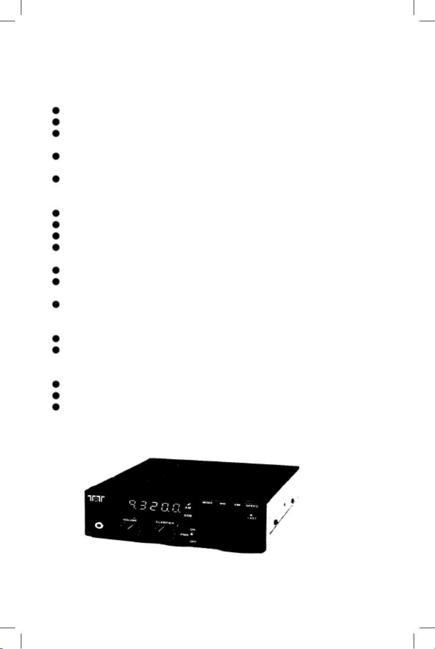
Model 1254 Receiver
Specifications and Features
Frequency coverage: 100 kHz to 30 MHz
Modes: AM, SSB/CW
Main Tuning: Normal or Fast tuning
(2.5 kHz SSB, 5.0 kHz AM, or 100 k Hz steps for either mode)
"Clarifier" Control: for ± 1.5 kHz SSB/CW fine tuning
between 2.5 kHz steps.
Front panel controls: On/off switch, Tuning, Volume, Clarifier,
Mode Select, Memory Write (MW),
VFO/Memory tuning select (V/M), Tuning Rate Select (SPEED)
Memories: 15 programmable memories
Circuit: Synthesized 45-75 MHz local oscillator
45 MHz first I-F, 455 kHz second I-F
Sensitivity: AM mode: 2.5 μV for 10 dB SNR at 30% modulation
SSB/CW mode: 0.5 μV for 10 dB SNR
Selectivity: 4 kHz @ -6 dB
Frequency/Memory Display: 6-digit green LED with mode indicators
Power supply: 12-15 VDC, 250 mA current consumption with no
signal present; 15VDC @ 800 mA wall transformer supply included
with kit.
Antenna connector: 50 ohm input, RCA-style phono jack
Audio: 1.5 watts audio output t o internal speaker, plus 1/8" stereo
phone jack for standard personal headphones or direct feed to 4-8
ohm external speaker, data inter face or both.
Semiconductors: 10 IC's, 26 transistors, 16 diodes
Compact Size: 2.25" x 6.5" x 6.5" ( HW D)
Construction: Steel clamshell case, aluminum chassis, custom-
molded front panel.
1254 - Reference - 2
Page 96
Model 1254 Receiver
3. Storing Frequencies in Memory
To place the currently displayed frequency and reception mode in
memory, do the following:
4. Recalling and Tuning Memory Frequencies
To scroll through or listen to the frequencies in memory:
Operating Instructions
1. Control Functions
The TUNE control performs two functions:
Direct frequency tuning
Memory Tuning (Memories 01 through 15)
The VOLUME control sets the rec eiver audio gain.
The CLARIFIER control permits fine-tuning of SSB and CW
signals within the 2.5 kHz tuning steps in SSB mode.
The POWER switch simply turns on the receiver on and off .
The [MODE] pushbutton selects between AM and CW-SSB
reception modes. The current mode is always shown in the
frequency display window.
The [MW] ("Memory write") button stores the current frequency
and reception mode in any memory location you choose. See
"storing Frequencies in Memory" for detailed instructions.
The [V/M] switch toggles between Frequency Tuning ("VFO")
and Memory Tuning. See "Tuning Mode Indicator" below.
When [V/M] is in Memory Tune mode, the Tuning Control is used
to select the desired memory.
The Tuning Mode Indicator is the LED decimal point to the right
of the last digit of the display. It is ON for direct frequency
tuning and OFF for memory tuning.
The [SPEED] button toggles the [FAST] 100 kHz step tuning
mode on and off as indicated by the FAST LED indicator.
2. Tuning AM Signals
Set the Clarifer control to its 12:00 position. Select AM with the
[MODE] button. The receiver will tune in 5 kHz steps unless
[FAST] 100 kHz tuning is selected. Adjusting the Clarifier
control may have a slight effect on signal quality but this control
is intended primarily for SSB-CW fine tuning.
1254 - Reference - 3
Page 97
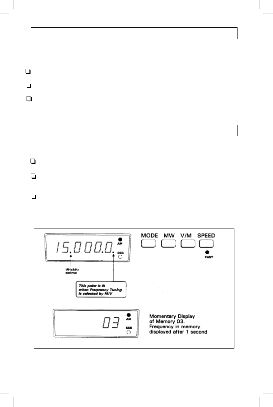
3. Storing Frequencies in Memory
To place the currently displayed frequency and reception mode in
memory, do the following:
Press [MW ]: the most-recently addressed memory
location will be displayed.
Rotate the TUNE control to the memory you wish to use,
either an empty location or to replace an unneeded frequency.
Press [MW ] again to store the frequency and return the
receiver to normal tuning mode.
4. Recalling and Tuning Memory Frequencies
To scroll through or listen to the frequencies in memory:
Press [V/M] to enter Memory Tune mode as indicated by the
Tuning Mode Indicator being toggled OFF by.
Rotate the tuning knob to selec t a memory location. The
display will momentarily indicate the location, then display the
stored frequency and reception mode.
Press [V/M] again to exit the memory tune mode and return to
the original VFO frequency
Figure 1R: Model 1254 Display and Mode Selection
1254 - Reference - 4
Page 98
5. Tuning SSB Signals
Model 1254 Receiver
Circuit Description
Before we begin a stage by stage description of the circuitry in
this receiver, let's take a broader view of how shortwave
receivers are designed in general. This should help show how
signals actually make their way from the antenna to the speaker.
Depending on their intended function, radio receivers can be
designed using several different electronic architectures. Very
simple receivers can be built from kits or your own parts using
classic autodyne, TRF, regenerative or direct-conversion designs.
Such receiver projects continue to provide t he fun of discovering
how radio originated and how simple it can be.
However, the most common approach used in short wave
receivers is called the superheterodyne method, usually referred
to as "superhet." In this approach, incoming signals from the
antenna are translated in frequency by a s pecial stage of circuitry
called a mixer. A radio frequency (RF) mixer is es sentially a high
speed switching circuit that combines the incoming signals with
a local oscillator ( LO) which is generated within the receiver.
This mixing process results in a frequency conversion to an
Intermediate Frequency (IF). A superhet receiver typically may
be single, double or triple conversion: the Model 1254 is a
double-conversion receiver with a 45 MHz first IF and a 455 kHz
second IF.
The simple receiver most closely related to the superhet is the
direct conversion design in which a variable LO is mixed with
incoming signals from the antenna. The resulting "IF" is in the
audio spectrum range and is amplified directly for listening.
The local oscillator must be a very clean and stable sinewave
because any undesirable characteristics on this signal would be
transferred to the rec eived signal by the mixing process. Most
modern receivers use a "synthesizer" to generate this signal. The
synthesizer circuit is able to tune the local oscillator in very
accurate steps and also hold the oscillator on frequency with
very little drift.
Mathematically, the mixer multiplies the instantaneous values of
the LO and the input together. The result is a pair of output
bands that are the sum and difference, in f requency, of t he input
and the LO. The LO frequency range is chosen so that one of
these bands can be separated out for further amplification and
Set the Clarifier control to its 12:00 position. Select SSB Mode
and tune to a signal of interest. Use the Clarifier control to adjust
for intelligible voice audio. Tune up (clockwise) for USB s ignals
and down for LSB signals. If you are tuning the Clarifier clockwise and the signal s till seems "out of reach," turn the Main
Tuning one step higher and then re-tune the desired signal.
Similarly, if you are tuning lower, then turn Main Tuning one step
lower.
6. Tuning CW and RTTY/Data Signals
Set the Clarifier control to its 12:00 position. Select SSB Mode
and tune to a signal of interest. Use the Clarifier control to
adjust for desired audio pitch. If you are tuning the Clarifier
clockwise and the signal still seems "out of reach," turn the Main
Tuning one step higher and then re-tune the desired signal with
the Clarifier. Similarly, if you are tuning lower, turn Main Tuning
one step lower"
7. Microprocessor RESET
A "power-on reset" is a quick way to clear all the memories. This
procedure can also be us ed to recover from fault conditions
caused perhaps by power supply line noise. The symptom or
evidence that somet hing is not right with the microprocessor can
be an unusual or blank frequency display or locked-up tuning. To
RESET the micr oprocessor, do the following:
Turn off the front panel DC power switch
Press and hold down both [MODE] and [MW]
Turn ON the power switch
Release [MODE] and [MW ] pushbuttons
Expect to see the 15.000 MHz default display
Reprogram the memory channels as desired
8. Memory Battery Test
At intervals comfortable to you, at least once a year, check the
condition of the memory backup battery with your VOM/DVM or
a reliable battery tester. To pres erve stored memories, the
battery removal, test and replacement should be done (carefully!)
while the receiver is TURNED ON.
1254 - Reference - 5
Page 99

Model 1254 Receiver
Circuit Description
Before we begin a stage by stage description of the circuitry in
this receiver, let's take a broader view of how shortwave
receivers are designed in general. This should help show how
signals actually make their way from the antenna to the speaker.
Depending on their intended function, radio receivers can be
designed using several different electronic architectures. Very
simple receivers can be built from kits or your own parts using
classic autodyne, TRF, regenerative or direct-conversion designs.
Such receiver projects continue to provide t he fun of discovering
how radio originated and how simple it can be.
However, the most common approach used in short wave
receivers is called the superheterodyne method, usually referred
to as "superhet." In this approach, incoming signals from the
antenna are translated in frequency by a s pecial stage of circuitry
called a mixer. A radio frequency (RF) mixer is es sentially a high
speed switching circuit that combines the incoming signals with
a local oscillator ( LO) which is generated within the receiver.
This mixing process results in a frequency conversion to an
Intermediate Frequency (IF). A superhet receiver typically may
be single, double or triple conversion: the Model 1254 is a
double-conversion receiver with a 45 MHz first IF and a 455 kHz
second IF.
The simple receiver most closely related to the superhet is the
direct conversion design in which a variable LO is mixed with
incoming signals from the antenna. The resulting "IF" is in the
audio spectrum range and is amplified directly for listening.
The local oscillator must be a very clean and stable sinewave
because any undesirable characteristics on this signal would be
transferred to the rec eived signal by the mixing process. Most
modern receivers use a "synthesizer" to generate this signal. The
synthesizer circuit is able to tune the local oscillator in very
accurate steps and also hold the oscillator on frequency with
very little drift.
Mathematically, the mixer multiplies the instantaneous values of
the LO and the input together. The result is a pair of output
bands that are the sum and difference, in f requency, of t he input
and the LO. The LO frequency range is chosen so that one of
these bands can be separated out for further amplification and
1254 - Reference - 6
Page 100
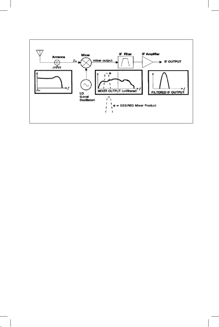
processing. This is illustrated with some example spectrum plots
Figure 3R: Model 1254 Block Diagram
in Figure 2R.
Fig. 2R: Spectrum Plot examples
The stage of selectivity and gain that follows the mixer is called
the intermediate frequency (IF) amplifier. Notice how the
position of the loc al oscillator determines which part of the
incoming spectrum falls within the bandwidth of the IF amplifier.
As the LO is tuned, individual signals can be separated out for
amplification and detection.
The typical receiver will use at least two mixers and two of these
intermediate frequency stages to convert an incom ing signal
down to audio. The desired tuning range of the receiver and the
availability of certain standard filter frequencies is usually what
determines the selection of the IF frequencies.
Let's now study the Block Diagram of the Model 1254 receiver
shown in Figure 3R. We will follow the signal path from antenna
to speaker, and explain the reasoning behind the design of each
stage.
1254 – Reference - 7
 Loading...