

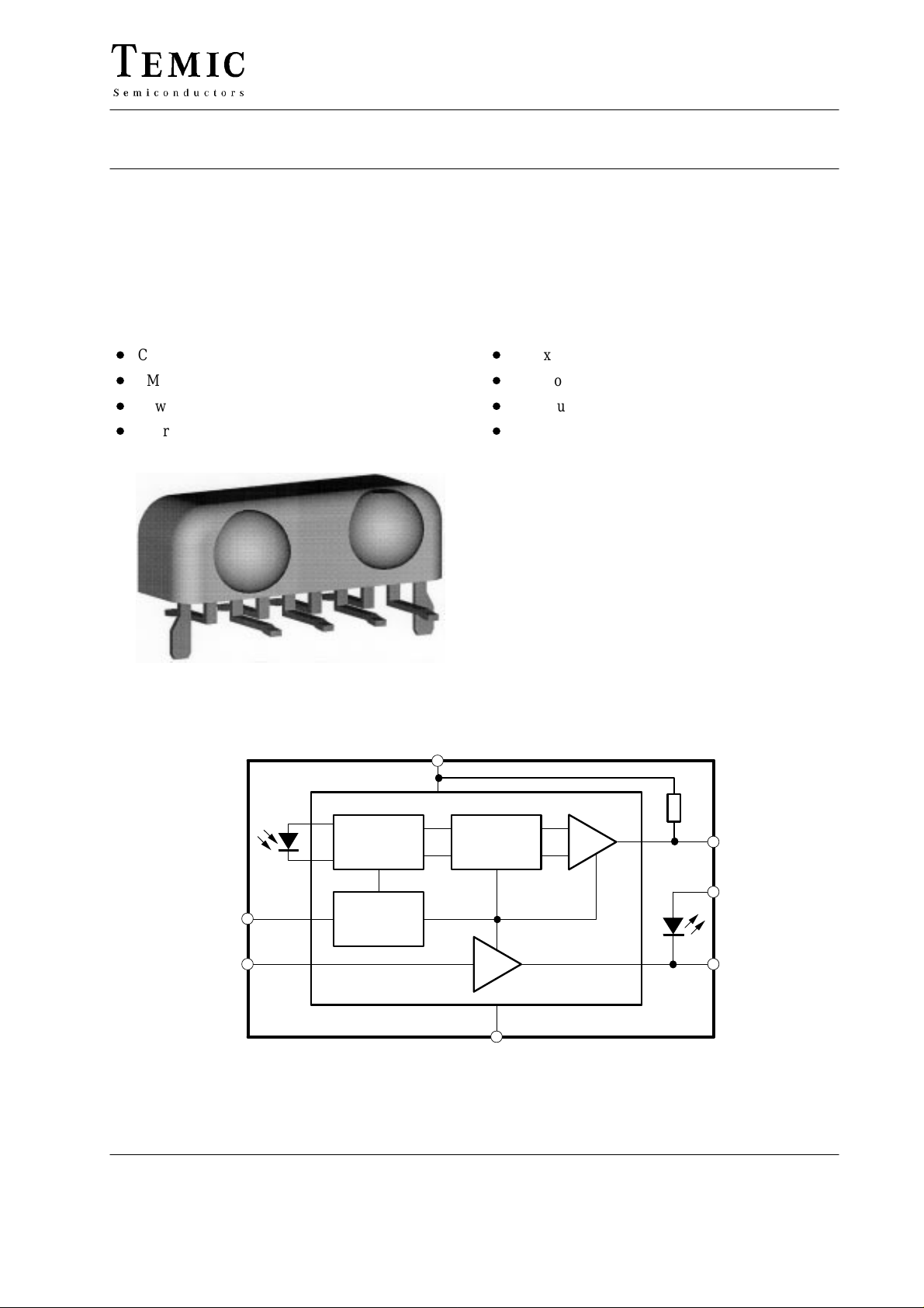
TFDS3000
Integrated Infrared Transceiver Module IrDA (SIR)
Description
The TFDS3000 is an infrared transceiver for data communication systems. The transceiver is compatible to the
IrDA standard which allows data rates up to 115 kB/s.
Features
D
Compatible to IrDA standard
D
SMD side view
D
Low profile (height = 5.6 mm max.)
D
Microcomputer compatible
An internal AGC (Automatic Gain Control) ensures
proper operation under EMI conditions.
D
No external components
D
Low power consumption
D
Wide supply voltage range (3 to 5.5 V)
D
AGC for EMI immunity
Pin description:
1: IRED cathode
2: Rxd (output)
3: V
4: Ground
5: NC
6: **)
7: Txd (input)
8: IRED anode
Guide pins internally connected to ground
(supply voltage)
CC
*)
SD
Txd
*) optional sensitivity control for OEMs only
**) shut-down, not for new development
V
cc
3
Driver
ComparatorAmplifier
6
7
Control
logic
Driver
4
GND
Figure 1. Block diagram
95 11227
2
Rxd
8
1
TELEFUNKEN Semiconductors
Rev . A6, 15-Aug-96
1 (10)
Preliminary Information
TFDS3000
Absolute Maximum Ratings
Reference point Pin 4, unless otherwise specified
Parameter Test Conditions Symbol Value Unit
Supply voltage range V
CC
Input currents All pins, exept 8:see IRED 10 mA
Output sinking current 25 mA
Power dissipation See figure 3 P
Junction temperature T
Ambient temperature range
T
tot
j
amb
(operating)
Storage temperature range T
stg
Soldering temperature See figure 11 introductory text
IrDA Design Guide
Average IRED current I
Repetitive pulsed IRED current < 90 ms, ton < 20% I
Peak IRED current < 2 ms, ton < 10% I
IRED anode voltage V
Transmitter data input voltage V
Receiver data output voltage V
(DC) 100 mA
IRED
(RP) 500 mA
IRED
(PK) 1 A
IRED
IREDA
Txd
Rxd
–0.5 to 6 V
200 mW
125 °C
0 to70 °C
–25 to +85 °C
230 (typ. 215)
–0.5 to V
–0.5 to V
–0.5 to V
+0.5 V
CC
+0.5 V
CC
+0.5 V
CC
_
C
Basic Characteristics
T
= 25_C, VCC = 5 V, unless otherwise specified
amb
Parameter Test Conditions Symbol Min. Typ. Max. Unit
T ransceiver
Supported data rates 2.4 115.2 kBit/s
Supply voltage range
reduced function down
to 2.6 V
Supply current I
Receiver
Min. detection threshold
irradiance
**)
Max. detection threshold
irradiance
**)
a
= "15° E
a
= "90° E
Logic low receiver input
irradiance
Max. DC irradiance
a
= "90° E
Output voltage Rxd Active,
C = 15 pF, R = 2.2 k
W
Output voltage Rxd Non-active,
C = 15 pF, R = 2.2 k
W
Output current VOL < 0.5 V
C = 15 pF, R = 2.2 k
Rise and fall time C = 15 pF, R = 2.2 k
Rxd signal, electrical
2.4 kB/s 1 20
W
W
output pulse width
Rxd signal, electrical
115.2 kB/s 1 8
output pulse width
**) BER = 10–8 is target of IrDA specification, defined sensitivities not related to BER = 10
V
emin
emax
E
emaxlow
edcmax
V
V
OH
tr, t
CC
S
3 5 5.5 V
1.3 2.5 mA
0.025 0.035 W/m
3300 5000 W/m
400 W/m
OL
0.5 0.8 V
VCC–0.5 V
4 mA
f
20 200 ns
–8
0.004 W/m
m
m
2
2
2
2
s
s
2 (10)
TELEFUNKEN Semiconductors
Rev . A6, 15-Aug-96
Preliminary Information
TFDS3000
Parameter Test Conditions Symbol Min. Typ. Max. Unit
Output delay time (Rxd)
Max. delay of leading
edge of output signal
related to leading edge
of optical input signal
Jitter, leading edge of
output signal
Output delay time (Rxd)
Max. delay of trailing
edge of output signal
related to trailing edge
of optical input signal
Latency Recovery from last
Transmitter
Supply voltage
switching specs only
cover 4.5 to 5.5 V
Driver Current IRED
I
can be adjusted by
d
variation of R
S
Logic low transmitter
input voltage
Logic high transmitter
input voltage
Output radiant intensity
= "15°
Angle of half intensity
Peak wavelength of
emission
Halfwidth of emission
spectrum
Optical rise / fall time 115.2 kHz square wave
Output radiant intensity Logic LOW level 0.4
Overshoot, optical 25 %
Rising edge peak-to-peak
jitter
Output level = 0.5 V
@ Ee = 0.040 W/m
CC
2
Over a period of 10 bit,
115.2 kB/s
Output level = 0.5 V
CC
transmitted pulse to
1.1 threshold sensitivity
Current limiting resistor in
series to IRED:
R
= 10
S
5 V
Max. input current
I
< 100 A
in
Current limiting resistor in
series to IRED: R
V
= 5 V
CC
= 10 ,
S
signal (1:1)
Over a period of 10 bits,
independent of information
content
1 2
2
6.5
t
L
V
CC
I
d
3 5.5 V
100 800
0.3 0.5 A
VIL(Txd) 0 0.8 V
VIH(Txd) 2.4 V
CC
40 60 200 mW/sr
p
850 870 900 nm
"
24 °
60 nm
200 600 ns
W/sr
t
j
0.2
s
s
s
s
V
s
TELEFUNKEN Semiconductors
Rev . A6, 15-Aug-96
3 (10)
Preliminary Information

TFDS3000
Recommended SMD Soldering Pads for TFDS3000
Dimensions in mm
11.75
5.08
2.54
8765
2.54
1.8
600
500
400
300
200
IF = 500 mA
IF = 400 mA
IF = 300 mA
+0.1
1
(2 )
0.63 1.0
1 234
94 8731
2.54 2.54
0.63
8.25
5.08
Figure 2.
Current derating as a
function of the maximum
forward current of IRED,
max. duty cycle
Peak operating current ( mA )
100
IF = 100 mA
0
0 20 40 60 80 100 120 140
Temperature ( °C )95 10103
Figure 3. Current derating as a function of ambient
temperature, condition: duty cycle v20%
4 (10)
Preliminary Information
TELEFUNKEN Semiconductors
Rev . A6, 15-Aug-96

TFDS3000
120
110
100
90
80
70
60
50
40
30
Relative output intensity (%)
20
10
0
–60–50–40–30–20–10 0 10 20 30 40 50 60
Angle (deg)96 11747
Figure 4.
120
110
100
90
80
70
60
50
40
30
Relative sensitivity (%)
20
10
0
–60–50–40–30–20–10 0 10 20 30 40 50 60
Angle (deg)96 11748
120
110
Vcc = 5 V, Rs = 10
100
90
80
Vcc=4V,Rs=10
70
60
50
40
Intensity (mW/sr)
30
Vcc = 3 V, Rs = 10
20
10
0
0 102030405060708090100
W
W
W
Temperature ( °C )96 11745
Figure 6.
30
25
2
20
15
10
5
Threshold irradiance (mW/m )
0
0 102030405060708090100
Vcc = 3 V
Vcc = 4 V
Vcc = 5 V
Temperature ( °C )96 11746
Figure 5.
TELEFUNKEN Semiconductors
Rev . A6, 15-Aug-96
Figure 7.
5 (10)
Preliminary Information

TFDS3000
TFDS3000 Recommended Circuit Diagram
V
S
Rxd
100
R
2
W
1
2
TFDS3000
IRED
Cathode
Rxd
IRED
Anode
Txd
R
3
5
W
8
7
Txd
GND
220 nF
C
3
2.2 k
C
R
4
W
1
4.7 mF
220 nF
Figure 8.
Txd is recommended to be dc-coupled to the driving
circuitry. R4 and C3 are only necessary if the input signal
is active for longer periods. This might occur under
certain conditions when the circuit is conncted to the NSC
or SMC Super I/OsTM. See National Semiconductors
application note.
R3 is used for controlling the current through the IR
emitter. To increase the output power, reduce the value.
V
3
CC
C
2
4
GND
SD
NC
6
5
95 11800
To reduce the output power, increase the value as
described in the TEMIC IrDA Design Guide.
The load resistor R1 is optional when longer cables must
be driven. Internally, RxD is connected to V
by a 20 k
CC
load.
C1 and C2 are dependent on the quality of the supply
voltage. A combination of 6.8 mF with 100 nF will also
work in most cases.
W
Pin Pin Name Description I/O Active
1 IRED cathode IRED cathode, internally connected to driver transistor
2 Rxd Received data O LOW
3 Vcc Supply voltage
4 GND Ground
5 NC No connection
6 NC No connection
7 Txd Data to be transmitted I HIGH
8 IRED anode IRED anode
– 2 guide pins Internally connected to ground
6 (10)
TELEFUNKEN Semiconductors
Rev . A6, 15-Aug-96
Preliminary Information

Shape and Dimensions of Reel
2.5
1.5
TFDS3000
W
1
A
N
95 10518
Figure 9. Shape and dimensions of reel
12.90
12.75
TFDS3000
Version Tape Width “W” A N W
C1 24 ± 1 330 ± 1 100 ± 1.5 24.4 (+2/–0) 30.4
21.5
20.5
W
2
1
W
2 max
TELEFUNKEN Semiconductors
Rev . A6, 15-Aug-96
7 (10)
Preliminary Information

TFDS3000
Dimensions of Tape
8 (10)
12402
Figure 10. Dimensions of tape TFDS3000
TELEFUNKEN Semiconductors
Rev . A6, 15-Aug-96
Preliminary Information

Dimensions in mm
TFDS3000
96 11749
TELEFUNKEN Semiconductors
Rev . A6, 15-Aug-96
9 (10)
Preliminary Information

TFDS3000
Ozone Depleting Substances Policy Statement
It is the policy of TEMIC TELEFUNKEN microelectronic GmbH to
1. Meet all present and future national and international statutory requirements.
2. Regularly and continuously improve the performance of our products, processes, distribution and operating systems
with respect to their impact on the health and safety of our employees and the public, as well as their impact on
the environment.
It is particular concern to control or eliminate releases of those substances into the atmosphere which are known as
ozone depleting substances (ODSs).
The Montreal Protocol ( 1987) and its London Amendments (1990 ) intend to severely restrict the use of ODSs and
forbid their use within the next ten years. Various national and international initiatives are pressing for an earlier ban
on these substances.
TEMIC TELEFUNKEN microelectronic GmbH semiconductor division has been able to use its policy of
continuous improvements to eliminate the use of ODSs listed in the following documents.
1. Annex A, B and list of transitional substances of the Montreal Protocol and the London Amendments respectively
2. Class I and II ozone depleting substances in the Clean Air Act Amendments of 1990 by the Environmental
Protection Agency (EPA) in the USA
3. Council Decision 88/540/EEC and 91/690/EEC Annex A, B and C (transitional substances) respectively.
TEMIC can certify that our semiconductors are not manufactured with ozone depleting substances and do not contain
such substances.
We reserve the right to make changes to improve technical design and may do so without further notice.
Parameters can vary in different applications. All operating parameters must be validated for each customer
application by the customer. Should the buyer use TEMIC products for any unintended or unauthorized
application, the buyer shall indemnify TEMIC against all claims, costs, damages, and expenses, arising out of,
directly or indirectly, any claim of personal damage, injury or death associated with such unintended or
unauthorized use.
10 (10)
TEMIC TELEFUNKEN microelectronic GmbH, P.O.B. 3535, D-74025 Heilbronn, Germany
Telephone: 49 (0)7131 67 2831, Fax number: 49 (0)7131 67 2423
TELEFUNKEN Semiconductors
Rev . A6, 15-Aug-96
Preliminary Information
 Loading...