

Telit Communications S p A LN931NAG User Manual
LN931-NAG
Hardware Specification
- 1 -

1.
1.1
1.2
1.3
1.4
2.
CONTENTS
GENERAL DESCRIPTION....................................................................4
SYSTEM MAIN FEATURE ....................................................................5
SYSTEM BLOCK DIAGRAM ................................................................8
PIN DEFINITION .....................................................................................9
PLATFORM CONNECTION DESIGN ............................................... 14
HARDWARE FEATURES ................................................................... 22
2.1 MOBILE DATA MODEM ............................................................................ 22
2.2 RF TRANSCEIVER ..................................................................................... 23
2.3 POWER MANAGEMENT IC ...................................................................... 23
2.4 ANTENNA DESIGN .................................................................................... 24
3.
MECHANICAL SPECIFICATIONS .................................................... 27
3.1 OVERVIEW .................................................................................................. 27
3.2 MECHANICAL CONSTRAINTS ................................................................ 27
3.3 M.2 CARD ASSEMBLY .............................................................................. 28
3.4 CONNECTOR ASSEMBLY ....................................................................... 29
4.
ELECTRICAL SPECIFICATIONS ...................................................... 30
4.1 RECOMMENDED OPERATING CONDITIONS ...................................... 30
4.2 POWER CONSUMPTION .......................................................................... 30
5.
RF PERFORMANCE SPECIFICATIONS .......................................... 31
- 2 -

5.1 RF MAXIMUM TX POWER SPECIFICATIONS ...................................... 31
5.2 RF MIN. RX SENSITIVITY SPECIFICATIONS ........................................ 32
6.
SOFTWARE REQUIREMENTS.......................................................... 33
- 3 -

1. General Description
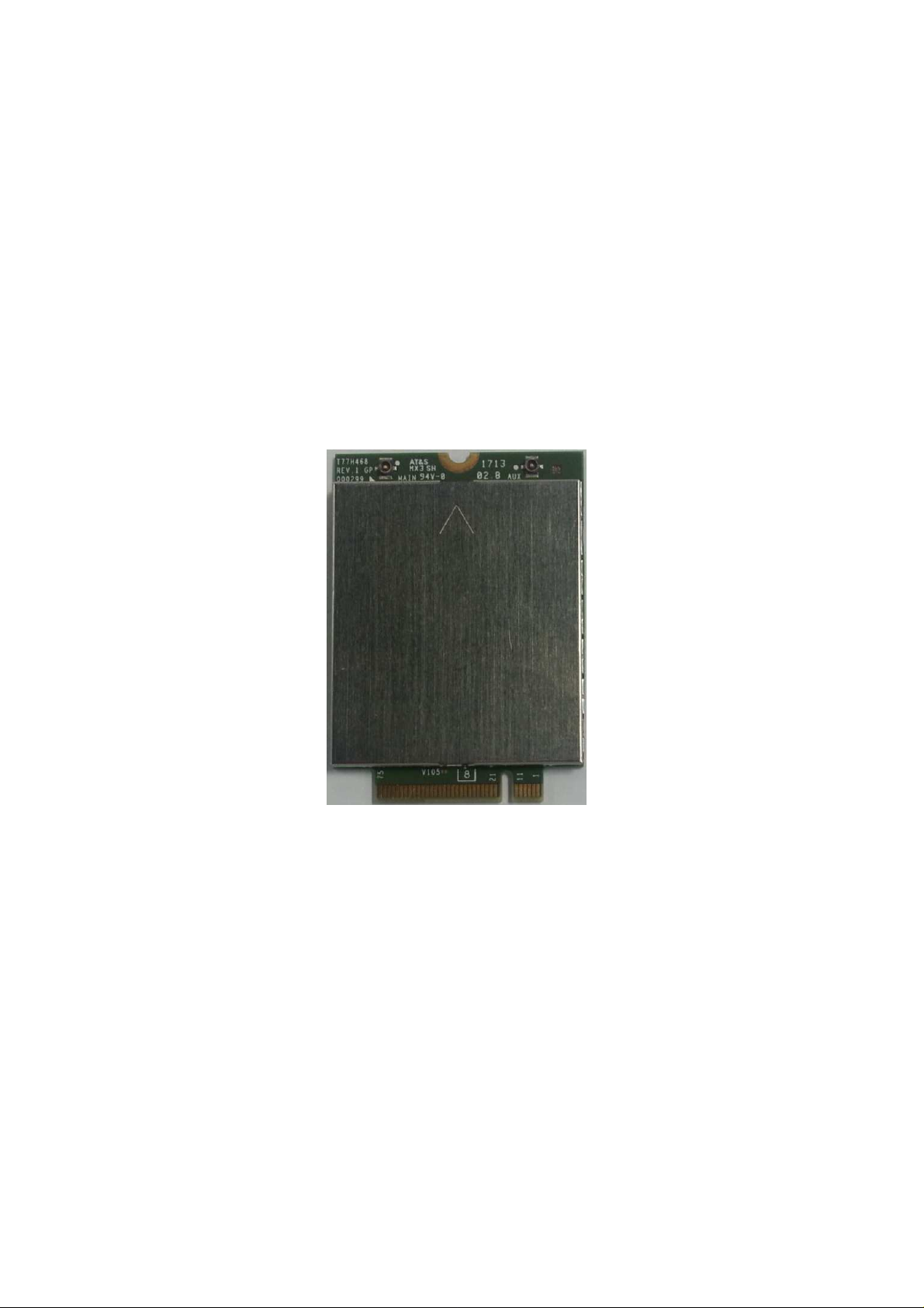
T77H468 is designed to enable wireless data connectivity for notebook computer or any
other device compatible with the PCI Express M.2 Specification 3042 type slot. T77H468 is
the data card solution that delivers wireless wide-area network (WWAN) connectivity for the
LTE, UMTS (HSDPA/HSUPA/HSPA+/DC-HSPA+), CDMA 1xRTT/CDMA EV-DOrA/ CDMA
EVDO-rB, GSM/GPRS/EDGE and GPS/Glonass protocols in one hardware configuration.
SKU NA-1-S3
WTR1605L
QUAD BAND BC 0,1 Band 1,2,4, 5,8 Band 2,4,5,13,17,25
TX_LB1 17
TX_LB2 850/900
TX_LB3 13
TX_LB4 0 5,8 5, 8r
TX_MB1 4 4
TX_MB2 1800/1900
TX_MB3 1 1,2 1r, 2,25
TX_MB4
TX_HB
PRX_LB1 13,17
PRX_LB2 850/900 8
PRX_LB3 0 5 5
PRX_MB1 1800/1900
PRX_MB2 1 2 2
PRX_MB3 1
PRX_HB 4 4
DRX_LB1 0 5,8 5
DRX_LB2 17
DRX_LB3 13
DRX_MB 1 2 2,25
DRX_HB 1,4 4
G C W L
4
Approximately
All
All CDMA 1X/CDMA EVDO
All
Antenna connectors
1.1 System Main Feature
Feature Description
Physical PCI express M.2 module, size 3042, 75Pin golden finger
Electrical Single VCC supply (3.3V+/-5% follow M.2 standard)
Dimension
Shielding design
Weight
Dimensions (L × W × H): 42 mm × 30 mm × 2.3 mm,
maximum height=2.38mm (add PCB tolerance=0.08mm)
Shield case on board design, no additional shielding
requirement
6.2g
USIM Off-board USIM connector supported
WCDMA/HSDPA/HSUPA/HSPA+ operating bands:
Band 1: 1920 to 1980 MHz (UL), 2110 to 2170 MHz (DL)
Band 2: 1850 to 1910 MHz (UL), 1930 to 1990 MHz (DL)
Band 4: 1710 to 1755 MHz (UL), 2110 to 2155 MHz (DL)
Band 5: 824 to 849 MHz (UL), 869 to 894 MHz (DL)
Band 8: 880 to 915 MHz (UL), 925 to 960 MHz (DL)
GSM operating bands:
GSM850: 824 to 849 MHz (UL), 869 to 894 MHz (DL)
E-GSM900: 880 to 915 MHz (UL), 925 to 960 MHz (DL)
DCS1800: 1710 to 1785 MHz (UL), 1805 to 1880 MHz (DL)
Operating Bands
PCS1900: 1850 to 1910 MHz (UL), 1930 to 1990 MHz (DL)
LTE FDD operating bands:
Band 2: 1850 to 1910 MHz (UL), 1930 to 1990 MHz (DL)
Band 4: 1710 to 1755 MHz (UL), 2110 to 2155 MHz (DL)
Band 5: 824 to 849 MHz (UL), 869 to 894 MHz (DL)
Band 13: 777 to 787 MHz (UL), 746 to 756 MHz (DL)
Band 17: 704 to 716 MHz (UL), 734 to 746 MHz (DL)
Band 25: 1850 to 1915 MHz (UL), 1930 to 1995 MHz (DL)
CDMA 1X/CDMA EV-DOrB operating bands:
BC0: 824 to 849 MHz (UL), 869 to 894 MHz (DL)
BC1: 1850 to 1910 MHz (UL), 1930 to 1990 MHz (DL)
WCDMA/HSDPA/HSUPA/HSPA+ operating bands
Diversity/2nd Rx
operating bands
LTE operating bands
GNSS
USIM Voltage Support 1.8V and 2.85V, and auto detects follow SIM card type
5
GPS: L1 (1575.42MHz)
GLONASS: L1 (1602MHz)
MAIN and AUX(supports Diversity and GPS simultaneously)

GPRS: DL 85.6 kbps /UL 85.6 kbps
EDGE: DL 236.8 kbps/UL 236.8 kbps
WCDMA CS: DL 64 kbps /UL 64 kbps
WCDMA PS: DL 384 kbps /UL 384 kbps
Throughput
HSPA+: DL 21.6 Mbps /UL 5.76 Mbps
DC-HSPA+ :DL 42 Mbps/UL 5.76 Mbps
CDMA 1x: DL 153.6 kbps/UL 153.6 kbps
EVDO Rev.A: DL 3.1 Mbps /UL 1.8 Mbps
EVDO Rev.B: DL 14.7 Mbps/UL 5.4 Mbps
LTE FDD:DL:100 Mbps/UL 50 Mbps @20M BW cat3
LTE air interface
LTE R9, Cat3, 20MHz BW (FDD: up to 100 Mbps downlink, 50 Mbps uplink)
FDD: up to 100 Mbps downlink, 50 Mbps uplink
1.4 to 20 MHz RF bandwidth
1X2 MISO (1Tx and 2Rx for two downlinks simultaneously)
IPv6, QoS
WCDMA/HSPA air interface
R99:
All modes and data rates for WCDMA FDD
R5 HSDPA
PS data speeds up to 7.2 Mbps on the downlink
R6 HSUPA
E-DCH data rates of up to 5.76 Mbps for 2 ms TTI (UE category 6) uplink
R7 HSPA+
Downlink 64 QAM; up to 21 Mbps
1X2 MISO (1Tx and 2Rx for two downlinks simultaneously)
2Rx with 16 QAM; up to 28 Mbps
Uplink 16 QAM; up to 5.76 Mbps
R8 DC-HSPA+
Downlink dual carrier with 64 QAM; up to 42 Mbps
CDMA air interface
1xRTT
153.6 kbps forward link, 153.6 kbps reverse link
1xEV-DOr0
High-speed peak data rates – 2.4 Mbps forward link; 153 kbps reverse link
1xEV-DOrA
High-speed peak data rates – 3.1 Mbps forward link; 1.8 Mbps reverse link
1xEV-DOrB
6

High-speed peak data rates – 14.7 Mbps forward link; 5.4 Mbps reverse link
GSM / GPRS / EDGE air interface
R99
Circuit-switched data: 9.6 k; 14.4 k
GPRS
Packet-switched data:
DTM (simple class A) operation
Multi-slot class 12 data services
CS schemes – CS1, CS2, CS3, and CS4
GEA1, GEA2, and GEA3 ciphering
Maximum of four Rx timeslots per frame
EDGE
E2 power class for 8 PSK
DTM (simple class A), multislot class 12
Downlink coding schemes – CS 1-4, MCS 1-9
Uplink coding schemes – CS 1-4, MCS 1-9
BEP reporting
SRB loopback and test mode B
8-bit and 11-bit RACH
PBCCH support
One-phase/two-phase access procedures
Link adaptation and IR
NACC, extended UL TBF
GNSS
GPS
Standalone, MS-A, MS-B, and XTRA GPS
Glonass
GLONASS standalone mode
GLONASS capability increases the number of satellites available to the positioning
engine, resulting in an expanded area of coverage over traditional GPS receivers
7

1.2 System Block Diagram
Figure 1-1 System block diagram
Chipsets: MDM9615+WTR1605L+PM8018
8
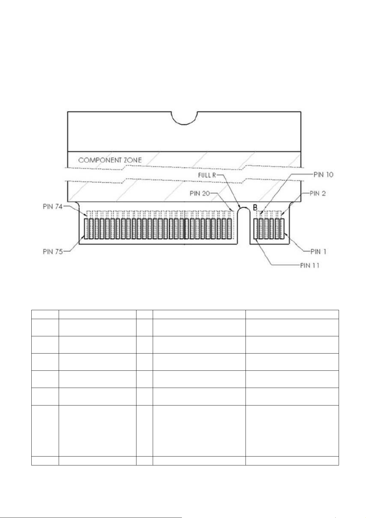
1.3 Pin definition
1.3.1 Golden finger Pin sequence
Figure 1-2 shows the sequence of pins on the 75-pin signal interface of M.2 3042.
1.3.2 Pin definition
Table 1-1 M.2 Pin definition
No. M.2 Pin name I/O Description Platform connection
1 CONFIG_3 O Connected to Ground
internally.
Refer to section ‘1.4.1
Configuration Pins ’
2 3.3V PI Power supply (3.3V+/-5%) Refer to section ‘1.4.2
Power and ground’
3 GND PI Ground Refer to section ‘1.4.2
Power and ground’
4 3.3V PI Power supply (3.3V+/-5%) Refer to section ‘1.4.2
Power and ground’
5 GND PI Ground Refer to section ‘1.4.2
Power and ground’
6 Full_Card_Power_Off
(0/1.8V or 0/3.3V)
I When it is Low, M.2 card
powers off.
Refer to section ‘1.4.3
Full_Card_Power_Off’
When it is High, M.2 card
powers on.
Pull down on card, should
be tolerant of 3.3V
7 USB_D+ IO USB Data+ defined in the Refer to section ‘1.4.4
9

USB 2.0 Specification. USB interface’
8 W_DISABLE#1
(0/3.3V)
I Active low signal used by
the host to turn on/off
Refer to section ‘1.4.5
W_DISABLE#’
radio operation.
When it is Low, radio off.
When it is High, radio on.
9 USB_D- IO USB Data- defined in the
USB 2.0 Specification.
10 LED#1 O Active low signal, used to
allow the M.2 card to
Refer to section ‘1.4.4
USB interface’
Refer to section ‘1.4.6
LED Indication’
provide status indicators
via LED devices that will
be provided by the
system.
11 GND PI Ground Refer to section ‘1.4.2
Power and ground’
12~19 Notch - Notch
20 AUDIO_0 - Don’t need to connect to
platform;
Connect to MDM9xxx
PRIM_PCM_CLK
21 CONFIG_0 O Not connect internally.
22 AUDIO_1 - Don’t need to connect to
platform;
Connect to MDM9xxx
PRIM_PCM_SYNC
23 WoWWAN (0/1.8V) O WWAN to wake up the
host, It is active low.
24 AUDIO_2 - Don’t need to connect to
platform;
Connect to MDM9xxx
PRIM_PCM_DIN
25 DPR (0/1.8V) I Hardware pin for
Reserve for future
extension, please contact
with us if need to use
these Pins
Refer to section ‘1.4.1
Configuration Pins ’
Reserve for future
extension, please contact
with us if need to use
these Pins
Refer to section ‘1.4.7
WoWWAN’
Reserve for future
extension, please contact
with us if need to use
these Pins
Refer to ‘1.4.8 DPR’
BodySAR Detection
H: No TX power backoff
(default)
L: TX power backoff
26 W_Disable2 I GPS disable:
H:Turn on
Refer to section ‘1.4.5
W_DISABLE#’
GPS/GLONASS (default)
L: Turn off
GPS/GLONASS
27 GND PI Ground Refer to section ‘1.4.2
Power and ground’
28 AUDIO_3 - Don’t need to connect to
platform;
Connect to MDM9xxx
PRIM_PCM_DOUT
Reserve for future
extension, please contact
with us if need to use
these Pins
10

29 SSIC-TxN - Don’t need to connect to
platform;
Connect to MDM9xxx
SPI_MOSI
Reserve for future
extension, please contact
with us if need to use
these Pins
30 UIM-RESET O UIM-RESET Refer to section ‘1.4.9
USIM’
31 SSIC-TxP - Don’t need to connect to
platform;
Connect to MDM9xxx
SPI_MISO
Reserve for future
extension, please contact
with us if need to use
these Pins
32 UIM-CLK O UIM-CLK Refer to section ‘1.4.9
USIM’
33 GND PI Ground Refer to section ‘1.4.2
Power and ground’
34 UIM-DATA IO UIM-DATA Refer to section ‘1.4.9
USIM’
35 SSIC-RxN - Don’t need to connect to
platform;
Connect to MDM9xxx
SPI_CS_N
Reserve for future
extension, please contact
with us if need to use
these Pins
36 UIM-PWR O UIM-PWR Refer to section ‘1.4.9
USIM’
37 SSIC-RxP - Don’t need to connect to
platform;
Connect to MDM9xxx
SPI_CLK
Reserve for future
extension, please contact
with us if need to use
these Pins
38 N/C - Not connect N/A for WWAN
39 GND PI Ground Refer to section ‘1.4.2
Power and ground’
40 GNSS_SCL (0/1.8V*) IO I2C_CLK, Don’t need to
connect to platform
Reserve for future
extension, please contact
with us if need to use
these Pins
41 NC - Don’t need to connect to
platform;
Connect to MDM9xxx
UART_CTS_N
42 GNSS_SDA
(0/1.8V*)
IO I2C_DATA, Don’t need to
connect to platform
Reserve for future
extension, please contact
with us if need to use
these Pins
Reserve for future
extension, please contact
with us if need to use
these Pins
43 NC - Don’t need to connect to
platform;
Connect to MDM9xxx
UART_RFR_N
44 GNSS_IRQ (0/1.8V*) IO I2C_IRQ, Don’t need to
connect to platform
Reserve for future
extension, please contact
with us if need to use
these Pins
Reserve for future
extension, please contact
with us if need to use
these Pins
11

45 GND PI Ground Refer to section ‘1.4.2
Power and ground’
46 SYSCLK (0/1.8V*) IO Don’t need to connect to
platform;
Connect to PMIC XO
Reserve for future
extension, please contact
with us if need to use
these Pins
47 NC - Don’t need to connect to
platform;
Connect to MDM9xxx
MDM_UART_TX
48 TX_BLANKING - Don’t need to connect to
platform;
Reserve for future
extension, please contact
with us if need to use
these Pins
Reserve for future
extension, please contact
with us if need to use
these Pins
49 NC - Don’t need to connect to
platform;
Connect to MDM9xxx
MDM_UART_RX
Reserve for future
extension, please contact
with us if need to use
these Pins
50 NC - Not connect N/A for WWAN
51 GND PI Ground Refer to section ‘1.4.2
Power and ground’
52 NC - Not connect N/A for WWAN
53 NC - Not connect N/A for WWAN
54 NC - Don’t need to connect to
platform;
Foxconn use internally to
separate different SKus
Connect to MDM9xxx
GPIO# internally
55 NC - Not connect N/A for WWAN
56 NC - Don’t need to connect to
platform;
Foxconn use internally to
separate different SKus
Connect to MDM9xxx
GPIO# internally
57 GND PI Ground Refer to section ‘1.4.2
Power and ground’
58 NC - Don’t need to connect to
platform;
Foxconn use internally to
separate different SKus
Connect to MDM9xxx
GPIO# internally
59 ANTCTL0 (0/1.8V) O Tunable antenna control
signal, bit 0
60 COEX3 (0/1.8V) - For LTE/WLAN
co-existence;
Refer to section ‘1.4.10
Antenna Control’
Refer to section ‘1.4.11
Coexistence’
LTE_WLAN_PRIORITY
61 ANTCTL1 (0/1.8V) O Tunable antenna control
signal, bit 1
62 COEX2 (0/1.8V) - For LTE/WLAN
co-existence;
Refer to section ‘1.4.10
Antenna Control’
Refer to section ‘1.4.11
Coexistence’
LTE_FRAME_SYNC
63 ANTCTL2 (0/1.8V) O Tunable antenna control Refer to section ‘1.4.10
12

signal, bit 2 Antenna Control’
64 COEX1 (0/1.8V) - For LTE/WLAN
co-existence;
Refer to section ‘1.4.11
Coexistence’
LTE_ACTIVE
65 ANTCTL3 (0/1.8V) O Tunable antenna control
signal, bit 3
Refer to section ‘1.4.10
Antenna Control’
66 SIM Detect I SIM_SWP Refer to section ‘1.4.9
USIM’
67 Reset# (0/1.8V) I System reset Refer to section ‘1.4.12
RESET#’
68 SUSCLK(32kHz)
(0/3.3V)
I Reserve Qualcomm MDM9xxx
solution don’t need
external SUSCLK
69 CONFIG_1 O Connected to Ground
internally.
Refer to section ‘1.4.1
Configuration Pins ’
70 3.3Vaux PI Power supply (3.3V+/-5%) Refer to section ‘1.4.2
Power and ground’
71 GND PI Ground Refer to section ‘1.4.2
Power and ground’
72 3.3Vaux PI Power supply (3.3V+/-5%) Refer to section ‘1.4.2
Power and ground’
73 GND PI Ground Refer to section ‘1.4.2
Power and ground’
74 3.3Vaux PI Power supply (3.3V+/-5%) Refer to section ‘1.4.2
Power and ground’
75 CONFIG_2 O Connected to Ground
internally.
Refer to section ‘1.4.1
Configuration Pins ’
13

1.4 Platform connection design
1.4.1 Configuration Pins
The M.2 module provides 4 configuration pins. T77H468 is configured as WWAN-SSIC 0,
refer to PCIe M.2_Rev0.7a.
Item Module configuration decodes Module type Port configuration
Config Config_0 Config_1 Config_2 Config_3
WWAN-SSIC 0 Pin No. 21 69 75 1
State NC GND GND GND
1.4.2 Power and ground
(1) Power Rail Parameters
Parameter Min Type Max Units
Operating voltage 3.135 3.3 3.465 Vdc
The operating voltage was defined in PCIe M.2_Rev0.7a standard as 3.3V+/-5%.
(2) 3.135 V is the minimum voltage supplied to LTE M.2 card by the host platform, and VCC
must never be under 3.135 V in any case. As our experiment, if we set the VCC=3.0V, the
M.2 card will power off when M.2 card working at +23dBm continue mode.
(3) Whenever the M.2 module works at 2G mode, the module transmits at the maximum
power (like +33dBm), the transient peak current may reach to 2.5 A.
We recommended design the VCC supply of host as below:
Remark: When the system power restarts, reserve R1 to discharge power.
(4) The LTE M.2 module provides 5 power pins and 11 Ground pins. To ensure that the LTE
module works normally, all the pins must be connected.
14
 Loading...