

Telit Communications S p A LN930 User Manual
xN930 M.2 Hardware User Guide
1VV0301078 Rev.6 – 2013-11-12
xN930 M.2 Hardware User Guide
APPLICABILITY TABLE
PRODUCT
LN930
LN930-AP
HN930
1VV0301078 Rev.6 – 2013-11-12
Reproduction forbidden without written authorization from Telit Communications S.p.A. - All Rights Reserved. Page 2 of 77

xN930 M.2 Hardware User Guide
1VV0301078 Rev.6 – 2013-11-12
SPECIFICATIONS SUBJECT TO CHANGE WITHOUT NOTICE
Notice
While reasonable efforts have been made to assure the accuracy of this document, Telit
assumes no liability resulting from any inaccuracies or omissions in this document, or from
use of the information obtained herein. The information in this document has been carefully
checked and is believed to be entirely reliable. However, no responsibility is assumed for
inaccuracies or omissions. Telit reserves the right to make changes to any products described
herein and reserves the right to revise this document and to make changes from time to time
in content hereof with no obligation to notify any person of revisions or changes. Telit does
not assume any liability arising out of the application or use of any product, software, or
circuit described herein; neither does it convey license under its patent rights or the rights of
others.
It is possible that this publication may contain references to, or information about Telit
products (machines and programs), programming, or services that are not announced in your
country. Such references or information must not be construed to mean that Telit intends to
announce such Telit products, programming, or services in your country.
Copyrights
This instruction manual and the Telit products described in this instruction manual may be,
include or describe copyrighted Telit material, such as computer programs stored in
semiconductor memories or other media. Laws in the Italy and other countries preserve for
Telit and its licensors certain exclusive rights for copyrighted material, including the
exclusive right to copy, reproduce in any form, distribute and make derivative works of the
copyrighted material. Accordingly, any copyrighted material of Telit and its licensors
contained herein or in the Telit products described in this instruction manual may not be
copied, reproduced, distributed, merged or modified in any manner without the express
written permission of Telit. Furthermore, the purchase of Telit products shall not be deemed
to grant either directly or by implication, estoppel, or otherwise, any license under the
copyrights, patents or patent applications of Telit, as arises by operation of law in the sale of a
product.
Computer Software Copyrights
The Telit and 3rd Party supplied Software (SW) products described in this instruction manual
may include copyrighted Telit and other 3rd Party supplied computer programs stored in
semiconductor memories or other media. Laws in the Italy and other countries preserve for
Telit and other 3rd Party supplied SW certain exclusive rights for copyrighted computer
programs, including the exclusive right to copy or reproduce in any form the copyrighted
computer program. Accordingly, any copyrighted Telit or other 3rd Party supplied SW
computer programs contained in the Telit products described in this instruction manual may
not be copied (reverse engineered) or reproduced in any manner without the express written
permission of Telit or the 3rd Party SW supplier. Furthermore, the purchase of Telit products
shall not be deemed to grant either directly or by implication, estoppel, or otherwise, any
license under the copyrights, patents or patent applications of Telit or other 3rd Party supplied
SW, except for the normal non-exclusive, royalty free license to use that arises by operation
of law in the sale of a product.
Reproduction forbidden without written authorization from Telit Communications S.p.A. - All Rights Reserved. Page 3 of 77

xN930 M.2 Hardware User Guide
1VV0301078 Rev.6 – 2013-11-12
Usage and Disclosure Restrictions
License Agreements
The software described in this document is the property of Telit and its licensors. It is
furnished by express license agreement only and may be used only in accordance with the
terms of such an agreement.
Copyrighted Materials
Software and documentation are copyrighted materials. Making unauthorized copies is
prohibited by law. No part of the software or documentation may be reproduced, transmitted,
transcribed, stored in a retrieval system, or translated into any language or computer language,
in any form or by any means, without prior written permission of Telit
High Risk Materials
Components, units, or third-party products used in the product described herein are NOT
fault-tolerant and are NOT designed, manufactured, or intended for use as on-line control
equipment in the following hazardous environments requiring fail-safe controls: the operation
of Nuclear Facilities, Aircraft Navigation or Aircraft Communication Systems, Air Traffic
Control, Life Support, or Weapons Systems (High Risk Activities"). Telit and its supplier(s)
specifically disclaim any expressed or implied warranty of fitness for such High Risk
Activities.
Trademarks
TELIT and the Stylized T Logo are registered in Trad em ark Office. All other product or
service names are the property of their respective owners.
Copyright © Telit Communications S.p.A. 2011.
Reproduction forbidden without written authorization from Telit Communications S.p.A. - All Rights Reserved. Page 4 of 77

xN930 M.2 Hardware User Guide
1 Introduction ......................................................................................................... 10
2 M.2 Overview ........................................................................................................ 13
3 M.2 Module Interface Details ............................................................................... 26
Contents
1VV0301078 Rev.6 – 2013-11-12
1.1 Scope .......................................................................................................................... 10
1.2 Purpose ...................................................................................................................... 10
1.3 Audience ..................................................................................................................... 10
1.4 Contact Information, Support .................................................................................... 10
1.5 Document Organization ............................................................................................. 11
1.6 Text Conventions ........................................................................................................ 11
1.7 Related Documents ................................................................................................... 11
2.1 SKUs - 2G/3G/LTE M.2 Modules ................................................................................ 13
2.2 M.2 Module – Block Diagrams ................................................................................... 17
2.2.1 M.2 HN930 Module ......................................................................................................... 17
2.2.2 M.2 LN930-AP Module ................................................................................................... 19
2.2.3 M.2 LN930 Module ......................................................................................................... 20
2.3 Host Interface Signals ............................................................................................... 21
3.1 USB 2.0 High-Speed – IPC Interface ......................................................................... 26
3.2 (U)SIM Interface ......................................................................................................... 27
3.3 GNSS Interface ........................................................................................................... 27
3.4 System Control Interface ........................................................................................... 30
3.4.1 Power On & Reset .......................................................................................................... 31
3.4.2 Host Radio Disable Operation ........................................................................................ 31
3.4.3 LED Interface – Status Indicator .................................................................................... 33
3.4.4 Wake on WWAN Signal ................................................................................................... 34
3.4.5 Dynamic Power Reduction ............................................................................................. 35
3.5 Tunable Antenna Control Interface ........................................................................... 37
3.6 In-Device Coexistence Interface ................................................................................ 38
3.7 Power Supply Interface .............................................................................................. 40
3.8 Trace & Debug Interface ............................................................................................ 40
Reproduction forbidden without written authorization from Telit Communications S.p.A. - All Rights Reserved. Page 5 of 77

xN930 M.2 Hardware User Guide
4 Development Tools ............................................................................................... 44
5 Windows Software Components ........................................................................... 49
6 Modem Configuration on Linux Based PC ............................................................. 51
7 Operating Environment ........................................................................................ 55
8 Power Delivery Requirements .............................................................................. 56
1VV0301078 Rev.6 – 2013-11-12
3.9 Configuration Pins ..................................................................................................... 41
3.10 Reserved Pins ............................................................................................................ 41
3.11 No Connect Pins ......................................................................................................... 42
3.12 Antenna Interface ...................................................................................................... 42
4.1 Carrier Board ............................................................................................................. 44
4.1.1 FlashTool........................................................................................................................ 45
4.1.2 PhoneTool ...................................................................................................................... 45
4.1.3 System Trace Tool .......................................................................................................... 46
4.1.4 RF Calibration ................................................................................................................ 46
4.1.5 Noise Profiling Scan Tool ............................................................................................... 47
4.1.6 GNSS Tools .................................................................................................................... 48
5.1 MBIM Toolkit .............................................................................................................. 50
5.1.1 Windows® 7 MBIM driver .............................................................................................. 50
5.1.2 GNSS UMDF driver for Windows® 7 and
5.1.3 M.2 module Firmware Update ....................................................................................... 50
5.1.4 End User Trace Tool....................................................................................................... 50
Windows® 8
................................................. 50
6.1 Overview ..................................................................................................................... 51
6.2 CMUX Multiplexer ...................................................................................................... 52
6.3 USB 2.0 HS Features .................................................................................................. 53
6.4 USB Configuration ..................................................................................................... 53
6.4.1 Modem Connection ........................................................................................................ 53
6.4.2 Network Connection ...................................................................................................... 53
6.4.3 Default Configuration ..................................................................................................... 54
6.5 LPM ............................................................................................................................ 54
6.5.1 Suspend/Resume and Remote Wake-up ....................................................................... 54
8.1 Electrical Parameters – 3.3 V Power Supply ............................................................. 56
Reproduction forbidden without written authorization from Telit Communications S.p.A. - All Rights Reserved. Page 6 of 77

xN930 M.2 Hardware User Guide
9 Other Information ................................................................................................ 60
10 WWAN Card Type 3042-S3-B ............................................................................. 64
11 Safety Recommendations .................................................................................. 69
12 Conformity assessment issues.......................................................................... 70
13 FCC/IC Regulatory notices ................................................................................ 74
14 Document History ............................................................................................. 76
1VV0301078 Rev.6 – 2013-11-12
8.2 Electrical Parameters - Host Interface Signals ........................................................ 57
8.3 Power Consumption ................................................................................................... 58
9.1 EMI/EMC and Platform Noise .................................................................................... 60
9.2 Platform Noise Mitigation - Adaptive Clocking ......................................................... 60
9.3 Thermal Monitoring ................................................................................................... 60
9.4 Seamless Roaming / Wifi Offload .............................................................................. 61
9.5 Conducted Transmit Power ....................................................................................... 61
9.6 Conducted Receiver Sensitivity .................................................................................. 61
9.7 Antenna Recommendations ...................................................................................... 62
10.1 Mechanical Dimensions ............................................................................................. 64
10.2 Land Pattern .............................................................................................................. 66
10.3 Antenna Connector Locations ................................................................................... 68
12.1 1999/5/EC Directive ................................................................................................... 70
12.2 CE RF Exposure Compliance ..................................................................................... 72
12.3 R&TTE Regulation:..................................................................................................... 73
13.1 Modification statement .............................................................................................. 74
13.2 Interference statement .............................................................................................. 74
13.3 FCC Class B digital device notice .............................................................................. 74
13.4 Radiation Exposure Statement .................................................................................. 75
13.5 End Product Labeling ................................................................................................ 75
Reproduction forbidden without written authorization from Telit Communications S.p.A. - All Rights Reserved. Page 7 of 77

xN930 M.2 Hardware User Guide
1VV0301078 Rev.6 – 2013-11-12
Figure 1 M.2 HSPA+ Block Diagram ................................................................................................................ 18
Figure 3
Figure 4 M.2 LTE Module Block Diagram........................................................................................................ 20
Figure 5 Detailed Interconnection of M.2 LTE Modem RF Engine .................................................................. 21
Figure 6 PCI Express M.2 Module Interface ..................................................................................................... 22
Figure 7
Figure 8 Typical LED Connection ..................................................................................................................... 34
Figure 9 Antenna Control – Connections Detail ................................................................................................ 37
Figure 10 In-Device Coexistence Architecture .................................................................................................. 38
Figure 11 RF Antenna – Coaxial Connector Location ....................................................................................... 43
Figure 12
Figure 13
Figure 14 Linux Software Architecture ............................................................................................................. 51
Figure 15
Figure 16
Figure 17 WWAN Card Type 3042 Top-Side Mounting Land Pattern with Key Removed ............................. 66
Figure 18 WWAN Card 3042 Mid-plane Land Pattern with Key Removed ..................................................... 67
Figure 19 Antenna Connector Location ............................................................................................................. 68
M.2 LTE Module Block Diagram
GNSS Connections and Interface
M.2 Carrier Board
Windows Software Architecture
WWAN Card 3042 Top/Bottom-View
WWAN Card 3042 Edge-View
.............................................................................................................................. 45
........................................................................................................ 19
........................................................................................................ 29
........................................................................................................ 49
.............................................................................................. 64
......................................................................................................... 65
Reproduction forbidden without written authorization from Telit Communications S.p.A. - All Rights Reserved. Page 8 of 77

xN930 M.2 Hardware User Guide
1VV0301078 Rev.6 – 2013-11-12
Table 1 M.2 Module - General Feature .............................................................................................................. 14
Table 2. M.2 Module - RF Band Support ......................................................................................................... 15
Table 3. M.2 Module - Data Services ............................................................................................................... 17
Table 4
Table 5 USB HS Interprocessor Communications In
Table 6
Table 7 X-GOLD™ Baseband to GNSS Interface Signals ................................................................................ 30
Table 8
Table 9
Table 10
Table 11 Host Radio Disable Interface (W_DISABLE#) .................................................................................. 33
Table 12
Table 13
Table 14
Table 15
Table 16
Table 17 Coexistence – Hardware Synchronization Signals .............................................................................. 39
Table 18
Table 19
Table 20
Table 21
Table 22
Table 23
Table 24 M.2 Module Power Delivery Requirements - Ultrabook .................................................................... 56
Table 25 VBAT Power Delivery Requirements – Direct Connections (Tablet) ................................................ 56
Table 26 Electrical Parameters – Host Interface Signals ................................................................................... 57
Table 27
Table 28
Table 29
Table 30 Conducted Transmit Power ................................................................................................................. 61
Table 31 Antenna Recommendation .................................................................................................................. 62
Table 32 Antenna Recommendation - Bandwidth of Main & Diversity Antenna ............................................. 62
M.2 Host Interface Signals
(U)SIM Interface Signals
GNSS Module Interface Signals
Power-on & Reset Signals
Radio Disable Signal
LED#1 Signal
LED State Indicator
Wake on WWAN Signal
DPR#/ SAR Support Signal
Tunable Antenna Control Signals
Power & Ground Signals
M.2 Configuration Pins
Reserved Pins
No Connect Pins
Antenna Requirements
Operating Environment
LTE Power Consumption
UMTS Power Consumption
GSM Power Consumption
...................................................................................................................................... 33
...................................................................................................................................... 41
................................................................................................................................. 42
.................................................................................................................... 22
ter
face .............................................................................. 26
...................................................................................................................... 27
........................................................................................................... 30
.................................................................................................................... 31
........................................................................................................................... 32
............................................................................................................................ 34
..................................................................................................................... 35
................................................................................................................ 36
....................................................................................................... 37
.................................................................................................................... 40
....................................................................................................................... 41
........................................................................................................................ 42
....................................................................................................................... 55
.................................................................................................................... 58
................................................................................................................ 58
.................................................................................................................. 58
Reproduction forbidden without written authorization from Telit Communications S.p.A. - All Rights Reserved. Page 9 of 77
xN930 M.2 Hardware User Guide
1
Introduction
1.1 Scope
1.2 Purpose
1.3 Audience
1.4 Contact Information, Support
This document is a technical specifi cat ion for Telit’s next generation form factor M.2 module
family. The next generation form factor M.2 module family is a natural transition from the
PCI Express Mini Card and Half Mini Card to a smaller form factor size.
The M.2 Card Type 3042 offers single sided component mounting, 75 pins (8 dedicated for
key), in a compact size (30 mm x 42 mm). A range of 2G/3G/4G (LTE) M.2 modules
supporting multiple operating systems and unique features in the WWAN Card Type 3042
form factor are available.
1VV0301078 Rev.6 – 2013-11-12
The document will cover the features of the M.2 modules presently available. It will also
identify the M.2 module application interface along with hardware, software, reliability, and
mechanical specifications.
The intent of this document is to provide design guidelines and information for each M.2
module.
In addition to the M.2 module family features and performance metrics, this document
describes the interface signals, operating conditions, physical and mechanical requirements of
the M.2 cards.
This document is intended for editors who are about to write or edit documentation for Telit.
For general contact, technical support, to report documentation errors and to order manuals,
contact Telit Technical Support Cent er ( TTSC) at:
TS-EMEA@telit.com
TS-NORTHAMERICA@telit.com
TS-LATINAMERICA@telit.com
TS-APAC@telit.com
Alternatively, use:
http://www.telit.com/en/products/technical-support-center/contact.php
For detailed information about where you can buy the Telit modules or for recommendations
on accessories and components visit:
Reproduction forbidden without written authorization from Telit Communications S.p.A. - All Rights Reserved. Page 10 of 77
xN930 M.2 Hardware User Guide
1.5 Document Organization
1.6 Text Conventions
1.7 Related Documents
http://www.telit.com
To register for product news and announcements or for product questions contact Telit
Technical Support Center (TTSC).
Our aim is to make this guide as helpful as possible. Keep us informed of your comments and
suggestions for improvements.
Telit appreciates feedback from the users of our information.
This document contains the following chapters (sample):
1VV0301078 Rev.6 – 2013-11-12
“Chapter 1: “Introduction”
support information, and text conventions.
“Chapter 2: “Chapter two” gives an overview of the features of the product.
“Chapter 3: “Chapter thr ee ” describes in details the characteristics of the product.
“Chapter 6: “Conformity Assessment Issues” provides some fundamental hints about the
conformity assessment that the final application might need.
“Chapter 7: “Safety Recommendation” provides some safety recommendations that must be
follow by the customer in the design of the application that makes use of the AA99-XXX.
Danger – This information MUST be followed or catastrophic equipment failure or bodily
injury may occur.
Caution or Warning – Alerts the user to important points about integrating the module, if
these points are not followed, the module and end user equipment may fail or malfunction.
provides a scope for this document, target audience, contact and
Tip or Information – Provides advice and suggestions that may be useful when
integrating the module.
All dates are in ISO 8601 format, i.e. YYYY-MM-DD.
• TBA
Reproduction forbidden without written authorization from Telit Communications S.p.A. - All Rights Reserved. Page 11 of 77

xN930 M.2 Hardware User Guide
1VV0301078 Rev.6 – 2013-11-12
.
Reproduction forbidden without written authorization from Telit Communications S.p.A. - All Rights Reserved. Page 12 of 77

xN930 M.2 Hardware User Guide
2
M.2 Overview
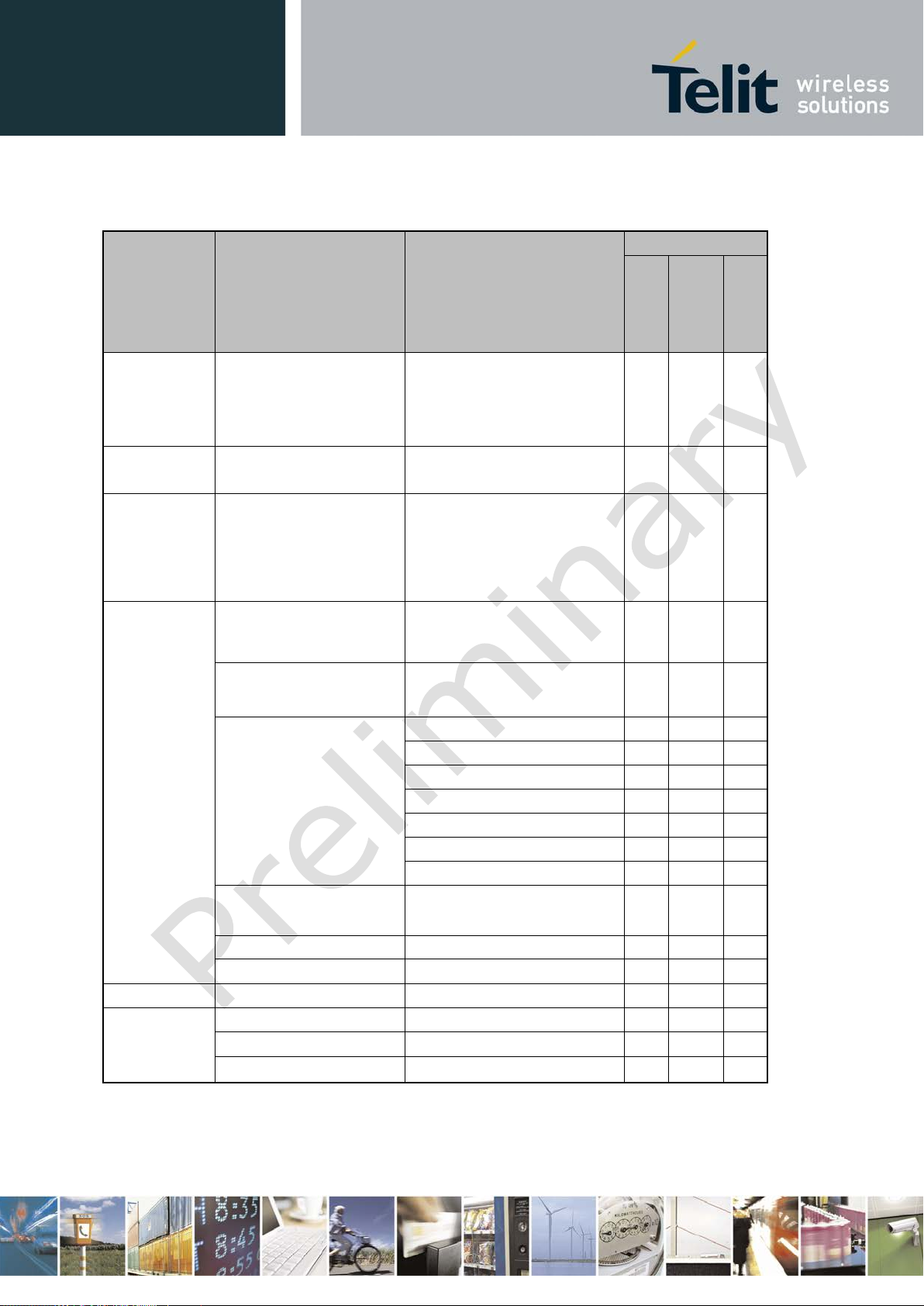
2.1 SKUs - 2G/3G/LTE M.2 Modules
This section will provide an overview of the standard features of a M.2 Card, information on
the various SKUs of 2G/3G/4G (LTE) M.2 modules along with a respective functional block
diagram of each SKU.
There are five different M.2 modules available in the M.2 C ard Type 3042 form factor:
• HN930 - HSPA+
• LN930-AP - APAC LTE
1VV0301078 Rev.6 – 2013-11-12
• LN930 - LTE
A comparison of the features, RF band Support, and data rates for the various M.2 modules is
shown in Table 1 through Table 3
Reproduction forbidden without written authorization from Telit Communications S.p.A. - All Rights Reserved. Page 13 of 77
xN930 M.2 Hardware User Guide
Feature
Description
Additional Information
M.2 module
Mechanical
M.2 Card Type 3042
30 mm x 42 mm
Operating
3.3 V Typical
-
Operating
-10˚C to +55˚C – Normal
xtreme - T his is the
Application
USB 2.0 High-speed
Interprocessor
USIM w/ Card Detect
SIM_CLK, SIM_RESET,
SIM_DETECT
M.2 Control
Full_Card_Power_On_Off
Reset#
x x x
W_DISABLE#
LED #1
x x x
DPR (Body SAR)
Wake on WWAN
x x x
GNSS Disable
Global Positioning
I2C_SCL, I2C_SDA, I2_IRQ,
Antenna Tuning
(4) GPO (RF Transceiver)
RF Coexistence
(3) GPIO
- x x
RF Antenna
Main & Diversity/ GNSS
Separate coax connectors
Debug
JTAG
-
x x x
ETM11
-
- x x
MIPI PTI
-
1VV0301078 Rev.6 – 2013-11-12
Table 1 M.2 Module - General Feature
Voltage
Temperature
Interface
(75 pin card)
Slot B
+55˚C to +70˚C –
Extended
Pin count: 75
(67 usable, 8 slot)
E
surrounding air temperature of
the module inside the platform
when the card is fully operating
at worst case condition
Communications
SIM_IO, SIM_PWR,
HN930
x x x
x x x
x x x
x x x
x x x
x x x
LN930-AP
LN930
Reproduction forbidden without written authorization from Telit Communications S.p.A. - All Rights Reserved. Page 14 of 77
(GPS/ GLONASS)
CLKOUT, TX_BLANKING
x x x
x x x
x x x
x x x
- x x
x x x
- x X
xN930 M.2 Hardware User Guide
RF Band
UE Transmit
UE Receive
M.2 Module
HN930
LN930-AP
LN930
001 I
1920 MHz -
2110 MHz -
002 II
1850 MHz -
1930 MHz -
003 III
1710 MHz -
1805 MHz -
004 IV
1710 MHz -
2110 MHz -
005 V
824 MHz -
869 MHz -
006 VI
830 MHz -
875 MHz -
007 VII
2500 MHz -
2620 MHz -
008 VIII
880 MHz -
925 MHz -
009 IX
1749.9 MHz -
1844.9 MHz -
010 X
1710 MHz -
2110 MHz -
011 XI
1427.9 MHz -
1475.9 MHz -
1VV0301078 Rev.6 – 2013-11-12
Table 2. M.2 Module - RF Ba n d Support
1980 MHz
1910 MHz
1785 MHz
1755 MHz
849 MHz
840 MHz
2170 MHz
1990 MHz
1880 MHz
2155 MHz
894 MHz
885 MHz
GSM
LTE
UMTS
GSM
LTE
UMTS
GSM
UMTS
x x x x x
x x x x x
x x x
x x x
x x
x
x x x
LTE
x
2570 MHz
915 MHz
1784.9 MHz
1770 MHz
1447.9 MHz
2690 MHz
960 MHz
1879.9 MHz
2170 MHz
1495.9 MHz
x
x x x x x x x
x x
x x
Reproduction forbidden without written authorization from Telit Communications S.p.A. - All Rights Reserved. Page 15 of 77
xN930 M.2 Hardware User Guide
012 XII
699 MHz -
729 MHz -
013 XIII
777 MHz -
746 MHz -
014 XIV
788 MHz -
758 MHz -
017 XVII
704 MHz -
7734 MHz -
018 XVIII
815 MHz -830
860 MHz -875
019 XIX
830 MHz -
875 MHz -
020 XX
832 MHz -
791 MHz -
021 XXI
1447.9 MHz -
1495.9 MHz -
022 XXII
3410 MHz -
3510 MHz -
023 XXIII
2000 MHz -
2180 MHz -
024 XXIV
1626.5 MHz -
1525 MHz -
025 XXV
1850 MHz -
1930 MHz 026 XXVI
814 MHz -
859 MHz -
027 XXVII
806 MHz -
851 MHz -
1VV0301078 Rev.6 – 2013-11-12
716 MHz
787 MHz
798 MHz
716 MHz
MHz
845 MHz
862 MHz
746 MHz
756 MHz
768 MHz
746 MHz
MHz
890 MHz
821 MHz
x
x
x x
x
x
x
1462.9 MHz
3490 MHz
2020 MHz
1660.5 MHz
1915 MHz
849 MHz
824 MHz
1510.9 MHz
3590 MHz
2200 MHz
1559 MHz
1995 MHz
894 MHz
869 MHz
x
x
Reproduction forbidden without written authorization from Telit Communications S.p.A. - All Rights Reserved. Page 16 of 77
xN930 M.2 Hardware User Guide
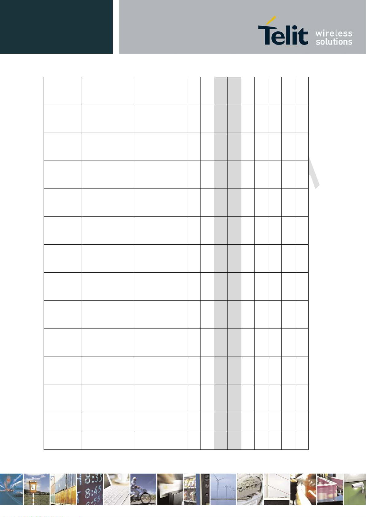
028 XXVIII
703 MHz -
758 MHz -
029 XXIX
1850 MHz -
716 MHz -
001 I
1920 MHz -
2110 MHz -
Data Service
M.2 module
GPRS Class 33: DL 85.6 kbps, UL 85.6 kbps
x - x
EDGE Class 33: DL 236.8 kbps, UL 236.8 kbps
x - x
WCDMA: DL 384 kbps, UL 384 kbps
x x x
HSPA+: DL 21 Mbps, UL 5.7 Mbps
x x x
HSPA+: DL 42 Mbps, UL 5.7 Mbps
- x x
LTE FDD: DL: 100 Mbps, UL 50 Mbps
- x x
2.2 M.2 Module – Block Diagrams
2.2.1 M.2 HN930 Module
1VV0301078 Rev.6 – 2013-11-12
748 MHz
1910 MHz
or
1710 MHz 1755 MHz
1980 MHz
803 MHz
728 MHz
2170 MHz
Table 3. M.2 Module - Data Services
HN930
LN930
LN930-AP
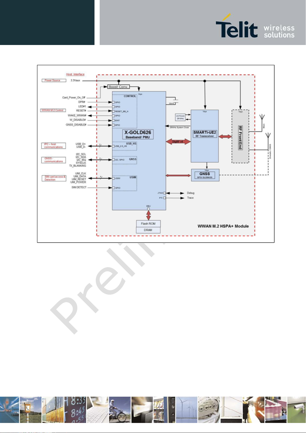
The M.2 HSPA+ module is Intel’s Next Generation Form Factor design based on Intel’s
XMM™6260 modem platform. The M.2 HSPA+ card is a dual-mode (UMTS/GSM) 3GPP
release 7 HSPA+ modem.
The M.2 HSPA+ module includes support at the 75 pin application interface for
Reproduction forbidden without written authorization from Telit Communications S.p.A. - All Rights Reserved. Page 17 of 77
M.2 Control, USB 2.0 HS, GNSS, and USIM. Antenna Tuning is not supported.
A block diagram of the M.2 HSPA+ module is shown in
Figure 1.
xN930 M.2 Hardware User Guide
1VV0301078 Rev.6 – 2013-11-12
Figure 1 M.2 HSPA+ Block Diagram
Reproduction forbidden without written authorization from Telit Communications S.p.A. - All Rights Reserved. Page 18 of 77

xN930 M.2 Hardware User Guide
2.2.2 M.2 LN930-AP Module
The M.2 APAC LTE module is another Intel design based on the XMM™7160 modem
platform. The module has a targeted area of operation in the Asia Pacific rim and offers 3G
and LTE datacard functionality, 2G Functionality is not supported.
The M.2 APC LTE module includes support at the 75 pin application interface for M.2
Control, USB 2.0 HS, GNSS, USIM and Antenna Tuning.
A block diagram of the M.2 APAC LTE module is shown in
1VV0301078 Rev.6 – 2013-11-12
Figure 2.
Figure 2
M.2 APAC LTE Module Block Diagram
Reproduction forbidden without written authorization from Telit Communications S.p.A. - All Rights Reserved. Page 19 of 77
xN930 M.2 Hardware User Guide
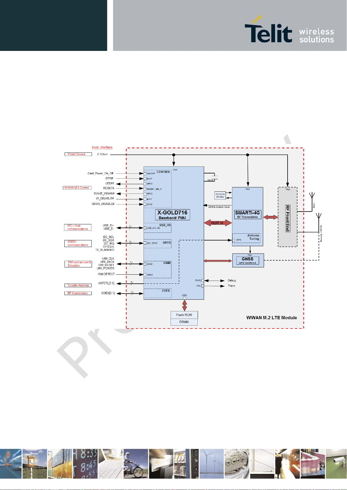
2.2.3 M.2 LN930 Module
The M.2 LTE module is based on Intel’s XMM™7160 modem platform. The M.2 LTE
module is a triple-mode (2G, 3G, and 4G) 3GPP release 9 modem providing datacard
functionality.
The M.2 LTE module includes support at the 75 pin application interface for
M.2 Control, USB 2.0 HS, GNSS, USIM and Antenna Tuning.
A block diagram of the M.2 LTE module is shown in
1VV0301078 Rev.6 – 2013-11-12
Figure 3.
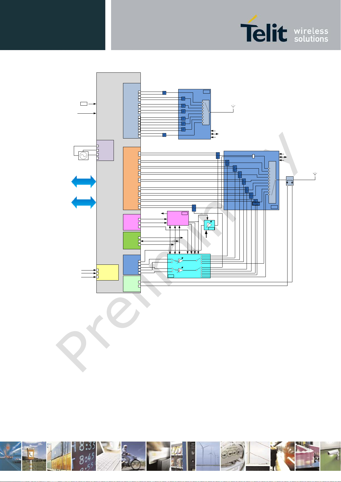
Figure 3 M.2 LTE Module Block Diagram
A more detailed interconnect diagram of the RF Engine utilized on the M.2 LTE Module is
shown in Figure 4.
Reproduction forbidden without written authorization from Telit Communications S.p.A. - All Rights Reserved. Page 20 of 77
xN930 M.2 Hardware User Guide
SMARTiTM 4G
PMB5740
RD_H1
RD_H1X
RD_H3
RD_H3X
RD
_M1
RD_M1
X
RD_L1
RD
_L
1X
RD_L2
RD_L2X
RD_L4
RD
_L
4X
Clock and
Control
DigRF
VBAT
SD
2
_1
V
8
AFC_DAC
REF OSC
XO_SUP
XO
VCTCXO
Measurement Unit
M1
M2
M3
Battery
RFE_NTC
RFE_PADCDC_MI
XOX
Diversity
Receiver
Combined
Receiver
RX_H2
RX
_H
2X
RX_H3
RX_H3X
RX
_H
4
RX_H4X
RX_M1
RX_
M1
X
RX_M2
RX
_M
2X
RX
_
L1
RX_
L1X
RX_L2
RX_L
2X
RX_
L4
RX_
L4X
RFFE
RFFE_
VIO
RFFE_SDATA
RFFE_SCLK
Transmitter
TQ_X
TQ_H
TQ_L
TP_H
TP_L
PA Control
PADACS
PADACF
PADACF
_P
FBR
FBR_RF1
FBR_RF2
XGOLDTM 716
B7
B1/B4
Diversity Switch &
Filter Module
Diversity
Antenna
RFE_RFFE_VIO
RFE_RFFE_SDATA
RFE_RFFE_SCLK
RFE_RFFE_VIO
RFE_RFFE_
SCLK
RFE_RFFE_
SDATA
Main Switch &
Duplexer Module
B7 Duplexer
B7 Div Filter
B
20 Div Filter
Coupler
Main
Antenna
RFE_RFFE_VIO
RFE_RFFE_SCLK
RFE_RFFE_SDATA
PA
DCDC
RFE
_TQ_
H
RFE_TP_H
RFE_TP_L
RFE_TQ_L
B2/B25
VBAT
VBAT
VBAT
RFE_VCC1_ET
RFE_VDD_ET
B7 PA
RFE
_PADCDC_
MI
SCPA
RD_M2
RD_M2X
RD_
L
3
RD_L3X
B
20
RX_
L3
RX_L
3X
B2/B25
B3
B
5/
B
26
B13/B17
B8
B20 Duplexer
B7
B20
B1
B4
B2/B25
B
3
B5/B26
B8
B13/
B17
B1
B
4
B3
GSM_HB
GSM_LB
B8
B5/B26
B20
B17
B13
RFE_PADACS
VBAT
RFFE CONTROL
VBAT
RFE_VBATAMP
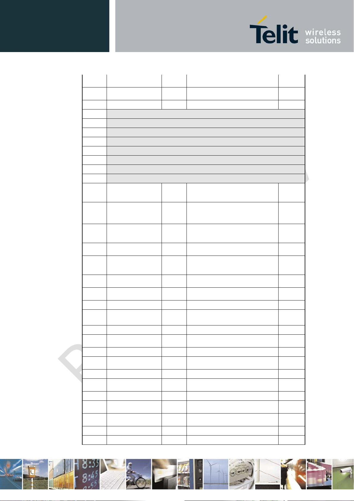
2.3 Host Interface Signals
1VV0301078 Rev.6 – 2013-11-12
Reproduction forbidden without written authorization from Telit Communications S.p.A. - All Rights Reserved. Page 21 of 77
Note that the M.2 module has all components mounted on the top side. Odd pin numbers are on the top
side while even pins on the bottom side.
Figure 4 Detailed Interconnection of M.2 LTE Modem RF Engine
This section describes the signals available to the host processor at the 75 pin application
interface. Eight signals are eliminated by the notch on the host connector, leaving 67 usable
signals. A diagram of the M.2 module identifying the 75 pin interface is shown in Figure 5.
xN930 M.2 Hardware User Guide
Pin
Signal Name
I/O
Description
Supply
1
2
3.3V
P
M.2 Supply Pin 3.3 V
3.3 V
3
GND
P
Ground
- 4 3.3V
P
M.2 LTE Supply Pin 3.3 V
3.3 V
5
GND
P
Ground
-
6
Card_Power_On_Off
I
Control signal to power On/Off
1.8 V
7
USB D+
IO
USB 2.0 HS DPLUS Signal
1.8
Pin
Signal Name
I/O
Description
Supply
8
W_DISABLE#
I
Active low signal to Disable Radio
3.3 V
1VV0301078 Rev.6 – 2013-11-12
Figure 5 PCI Express M.2 Module Interface
A complete description of all interface signals available at the host interface is listed in Table
4. Some features, such as GNSS and Antenna Tuning, are not available on every M.2 module.
On those modules, the signals at the application interface are not connected on the M.2
module.
Table 4
CONFIG_3 O Presence Indication:
M.2 Host Interface Signals
WWAN M.2 Connects to GND
internally
-
Reproduction forbidden without written authorization from Telit Communications S.p.A. - All Rights Reserved. Page 22 of 77
M.2.
V/2.9 V
Operation
xN930 M.2 Hardware User Guide
9
USB D–
IO
USB 2.0 HS DMINUS Signal
1.8
V/2.9 V
10
LED#1
O
Open Drain, active low signal used
3.3 V
11
GND
P
Ground
-
12
SLOT KEY
13
SLOT KEY
14
SLOT KEY
15
SLOT KEY
16
SLOT KEY
17
SLOT KEY
18
SLOT KEY
19
SLOT KEY
20
21
-
22
23
WAKE_WWAN#
O
Wake On WWAN
Use by M.2 to wake up host.
1.8 V
24
25
DPR#
I
Dynamic Power Reduction - Body
1.8 V
26
GNSS_DISABLE#
I
Disable GNSS function
1.8 V
27
GND
P
Ground
-
28
29
N/C - Not connected internally on M.2
-
30
UIM-RESET
O
SIM Reset (I)
1.8
V/2.9 V
31
N/C - Not connected internally on M.2
-
32
UIM-CLK
O
SIM Clock (I)
1.8
V/2.9 V
33
GND
-
Ground
-
34
UIM-DATA
IO
SIM Data (I/O)
1.8
V/2.9 V
35
N/C - Not connected internally on M.2
-
Pin
Signal Name
I/O
Description
Supply
36
UIM-PWR
O
SIM power (1.8 V/2.9 V)
1.8
37
N/C - Not connected internally on M.2
-
38
N/C - Not connected internally on M.2
-
1VV0301078 Rev.6 – 2013-11-12
for add-in card to provide status
AUDIO0 IO PCM Clock (I2S_CLK) - Future
development
CONFIG_0 O Configuration Status. Presently
not connected on WWAN M.2
module.
AUDIO1 I PCM In (I2S_RX) - Future
development
AUDIO2 O PCM Out (I2S_TX) - Future
development
SAR control signal
AUDIO3 IO PCM Sync (I2S_WA0) - Future
development
1.8 V
1.8 V
1.8 V
1.8 V
Reproduction forbidden without written authorization from Telit Communications S.p.A. - All Rights Reserved. Page 23 of 77
V/2.9 V
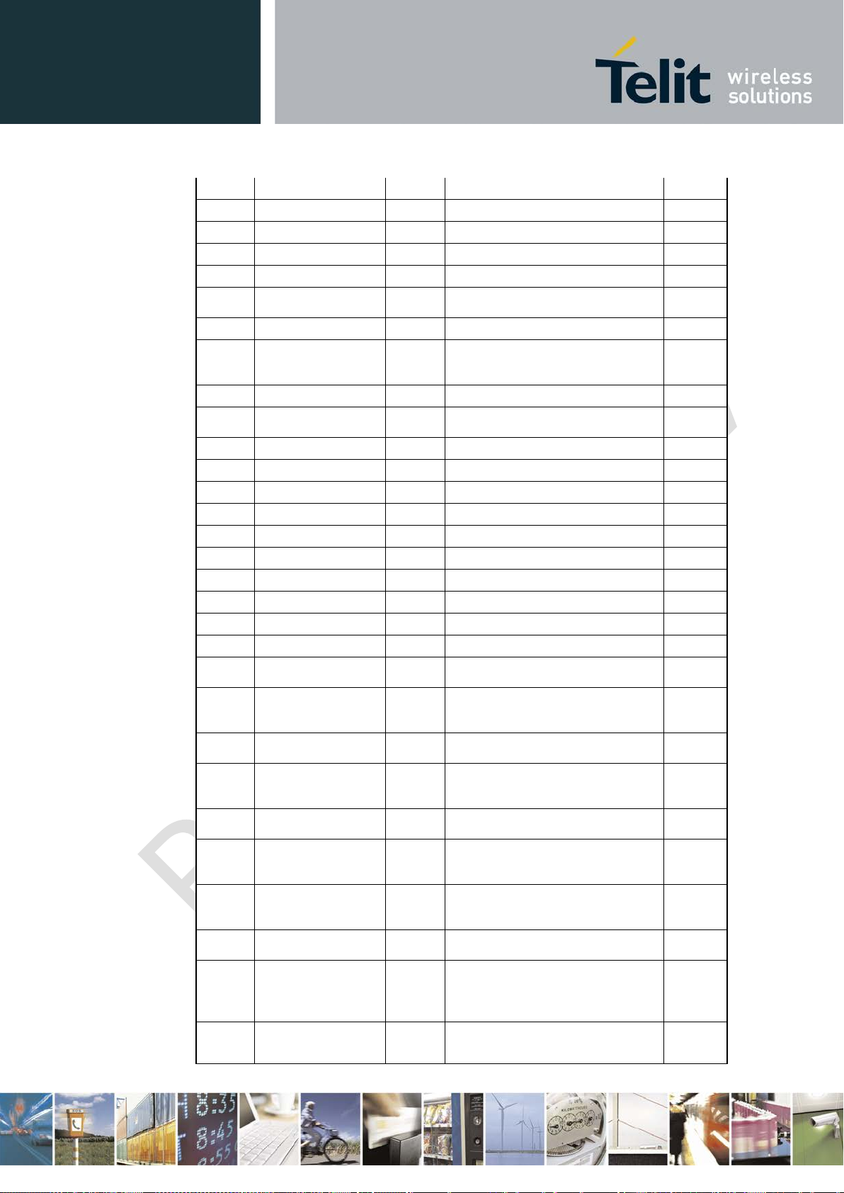
xN930 M.2 Hardware User Guide
39
GND
P
Ground
-
40
I2C_SCL
IO
I2C Clock – GNSS Support
1.8 V
41
N/C - Not connected internally on M.2
-
42
I2C_SDA
IO
I2C Data – GNSS Support
1.8 V
43
N/C - Not connected internally on M.2
44
I2C_IRQ
I
GNSS Interrupt Request – GNSS
1.8 V
45
GND
P
Ground
-
46
SYSCLK
O
26 MHz reference Clock output for
1.8 V
47
N/C - Not connected internally on M.2
-
48
TX_BLANKING
O
GNSS Blanking Signal used to
indicate 2G Tx burst.
1.8 V
49
N/C - Not connected internally on M.2
-
50
N/C - Not connected internally on M.2
-
51
GND
P
Ground
-
52
N/C - Not connected internally on M.2
-
53
N/C - Not connected internally on M.2
-
54
N/C - Not connected internally on M.2
-
55
N/C - Not connected internally on M.2
-
56
N/C - Not connected internally on M.2
-
57
GND
P
Ground
-
58
N/C - Not connected internally on M.2
-
59
ANTCTL0
I
RF Antenna Tuning Control Signal
1.7 V -
60
COEX0
-
Wireless Coexistence between
61
ANTCTL1
I
RF Antenna Tuning Control Signal
1
1.7 V -
2.6 V
62
COEX1
-
Wireless Coexistence between
63
ANTCTL2
I
RF Antenna Tuning Control Signal
1.7 V -
64
COEX2
Wireless Coexistence between
-
Pin
Signal Name
I/O
Description
Supply
65
ANTCTL3
I
RF Antenna Tuning Control Signal
3
1.7 V -
2.6 V
66
SIM DETECT
I
SIM Card Detection (I) (low
1.8 V
67
RESET#
I
Single control to reset WWAN (O)
designs)
1.8 V
1VV0301078 Rev.6 – 2013-11-12
Support
external GNSS
module
0
WWAN and WiFi/BT
modules
WWAN and WiFi/BT
modules
2
WWAN and WiFi/BT
modules
active).
• Pull-up resistor on WWAN M.2
module
(*not used on ULTRABOOK
2.6 V
2.6 V
Reproduction forbidden without written authorization from Telit Communications S.p.A. - All Rights Reserved. Page 24 of 77
 Loading...