

Telit Communications S p A LE940B6NA User Manual

LE940B6
Hardware User Guide
1VV0301331 Rev. 1.8 - 2017-03-15
LE940B6 Hardware User Guide
1VV0301331 Rev. 1.8 - 2017-03-15
This documentation applies to the following products:
Table 1: Applicability Table
Module Name Description
LE940B6-NA AUTO North America regional variant (AT&T and T-Mobile)
LE940B6-NV AUTO North America region variant (Verizon, AT&T and T-Mobile)
LE940B6-RW AUTO Rest of World variant (Europe, APAC, Latin America and more)
LE940B6-CN AUTO China variant
Note: NV variant - to be developed
Reproduction forbidden without written authorization by Telit Communications S.p.A. - All Rights Reserved
Telit Confidential Information, provided under NDA Page
2 of 104

LE940B6 Hardware User Guide
1VV0301331 Rev. 1.8 - 2017-03-15
SPECIFICATIONS SUBJECT TO CHANGE WITHOUT NOTICE
Notice
While reasonable efforts have been made to assure the accuracy of this document, Telit assumes
no liability resulting from any inaccuracies or omissions in this document, or from use of the
information obtained herein. The information in this document has been carefully checked and is
believed to be entirely reliable. However, no responsibility is assumed for inaccuracies or omissions.
Telit reserves the right to make changes to any products described herein and reserves the right to
revise this document and to make changes from time to time in the content hereof with no
obligation to notify any person of revisions or changes. Telit does not assume any liability arising
out of the application or use of any product, software, or circuit described herein; neither does it
convey any license under its patent rights or the rights of others.
It is possible that this publication may contain references to, or information about Telit products
(machines and programs), programming, or services that are not announced in your country. Such
references or information must not be construed to mean that Telit intends to announce such Telit
products, programming, or services in your country.
Copyrights
This instruction manual and the Telit products described in this instruction manual may be, include,
or describe copyrighted Telit material, such as computer programs stored in semiconductor
memories or other media. Laws in Italy and other countries preserve for Telit and its licensors
certain exclusive rights for copyrighted material, including the exclusive right to copy, reproduce in
any form, distribute, and make derivative works of the copyrighted material. Accordingly, any
copyrighted material of Telit and its licensors contained herein or in the Telit products described in
this instruction manual may not be copied, reproduced, distributed, merged, or modified in any
manner without the express written permission of Telit. Furthermore, the purchase of Telit
products shall not be deemed to grant either directly or by implication, estoppel, or otherwise, any
license under the copyrights, patents or patent applications of Telit, as arises by operation of law
in the sale of a product.
Computer Software Copyrights
Telit and third-party software (SW) products described in this instruction manual may include
copyrighted Telit and other third-party computer programs stored in semiconductor memories or
other media. Laws in Italy and other countries preserve for Telit and other third-party SW certain
exclusive rights for copyrighted computer programs, including the exclusive right to copy or
reproduce in any form the copyrighted computer program. Accordingly, any copyrighted Telit or
other third-party SW computer programs contained in the Telit products described in this
instruction manual may not be copied (reverse engineered) or reproduced in any manner without
the express written permission of Telit or the third-party SW supplier. Furthermore, the purchase
of Telit products shall not be deemed to grant either directly or by implication, estoppel, or
otherwise, any license under the copyrights, patents or patent applications of Telit or other thirdparty SW, except for the normal non-exclusive, royalty free license to use that arises by operation
of law in the sale of a product.
Reproduction forbidden without written authorization by Telit Communications S.p.A. - All Rights Reserved
Telit Confidential Information, provided under NDA Page
3 of 104

LE940B6 Hardware User Guide
1VV0301331 Rev. 1.8 - 2017-03-15
Usage and Disclosure Restrictions
License Agreements
The software described in this document is the property of Telit and its licensors. It is furnished by
an express license agreement only and may be used only in accordance with the terms of such an
agreement.
Copyrighted Materials
Software and documentation are copyrighted materials. Making unauthorized copies is prohibited
by law. No part of the software or documentation may be reproduced, transmitted, transcribed,
stored in a retrieval system, or translated into any language or computer language, in any form or
by any means, without prior written permission of Telit.
High Risk Materials
Components, units, or third-party products used in the product described herein are NOT faulttolerant and are NOT designed, manufactured, or intended for use as on-line control equipment in
the following hazardous environments requiring fail-safe controls: the operation of nuclear
facilities, aircraft navigation or aircraft communication systems, air traffic control, life support, or
weapons systems (“high risk activities"). Telit and its supplier(s) specifically disclaim any expressed
or implied warranty of fitness for such high risk activities.
Trademarks
TELIT and the stylized T logo are trademarks and/or registered trademarks of Telit Communications
S.p.A. in the Unites States and/or other countries. All other product or service names are the
property of their respective owners.
Copyright © 2016 Telit Communications S.p.A.
Reproduction forbidden without written authorization by Telit Communications S.p.A. - All Rights Reserved
Telit Confidential Information, provided under NDA Page
4 of 104

LE940B6 Hardware User Guide
1VV0301331 Rev. 1.8 - 2017-03-15
Contents
1.
Introduction ..................................................................................................... 12
2.
1.1. Scope ................................................................................................................ 12
1.2. Audience .......................................................................................................... 12
1.3. Contact Information, Support .......................................................................... 12
1.4. Text Conventions ............................................................................................. 13
1.5. Related Documents .......................................................................................... 14
1.6. Abbreviations ................................................................................................... 14
1.7. Document Organization ................................................................................... 15
General Product Description ............................................................................ 17
2.1. Overview .......................................................................................................... 17
2.2. Applications ..................................................................................................... 17
2.3. General Functionality and Main Features ....................................................... 18
2.4. Environmental Requirements .......................................................................... 19
2.4.1. Temperature Range .............................................................................. 19
2.4.2. RoHS Compliance.................................................................................. 19
3.
4.
2.5. Operating Frequency Bands............................................................................. 20
2.5.1. RF Bands per Regional Variant ............................................................. 20
2.5.2. Reference Table of RF Bands Characteristics ....................................... 21
2.6. Sensitivity ......................................................................................................... 24
2.7. LE940B6 Mechanical Specifications ................................................................. 25
2.7.1. Dimensions ........................................................................................... 25
2.7.2. Weight .................................................................................................. 25
LE940B6 Module Connections .......................................................................... 26
3.1. Pin-out .............................................................................................................. 26
3.2. LE940B6 Signals That Must Be Connected ...................................................... 36
3.3. LGA Pads Layout ............................................................................................... 38
Electrical Specifications .................................................................................... 39
4.1. Absolute Maximum Ratings – Not Operational ............................................... 39
Reproduction forbidden without written authorization by Telit Communications S.p.A. - All Rights Reserved
Telit Confidential Information, provided under NDA Page
5 of 104

LE940B6 Hardware User Guide
1VV0301331 Rev. 1.8 - 2017-03-15
5.
4.2. Recommended Operating Conditions ............................................................. 39
4.3. Logic Level Specifications ................................................................................. 40
4.3.1. 1.8V Standard GPIOs ............................................................................ 40
4.3.2. 1.8V I2C Pads ........................................................................................ 41
4.3.3. 1.2V EMIC Pads ..................................................................................... 41
4.3.4. 1.8V/2.9V SIM Pads .............................................................................. 42
4.3.5. USB........................................................................................................ 42
4.3.6. 2.5V/3.3V EMAC Interface for RMII and RGMII ................................... 43
Hardware Commands ....................................................................................... 44
5.1. Turning on the LE940B6 Module ..................................................................... 44
5.2. Initialization and Activation State .................................................................... 44
5.3. Turning off the LE940B6 Module ..................................................................... 48
5.3.1. Shutdown by Software Command ....................................................... 48
5.3.2. Hardware Shutdown ............................................................................. 50
6.
7.
5.3.3. Unconditional Hardware Reset (RESET_N)........................................... 51
5.3.4. Unconditional Hardware Shutdown ..................................................... 52
Power Supply ................................................................................................... 54
6.1. Power Supply Requirements............................................................................ 54
6.2. General Design Rules ....................................................................................... 57
6.2.1. Electrical Design Guidelines .................................................................. 57
6.2.1.1. + 5V Input Source Power Supply – Design Guidelines ......... 57
6.2.1.2. + 12V Input Source Power Supply – Design Guidelines ....... 58
6.2.1.3. Battery Source Power Supply – Design Guidelines .............. 60
6.2.2. Thermal Design Guidelines ................................................................... 61
6.2.3. Power Supply PCB Layout Guidelines ................................................... 61
Antenna(s) ....................................................................................................... 63
7.1. GSM/WCDMA/TD-SCDMA/LTE Antenna Requirements ................................. 63
7.2. GSM/WCDMA/TD-SCDMA/LTE Antenna – PCB Line Guidelines ..................... 63
7.3. GSM/WCDMA/TD-SCDMA/LTE Antenna – Installation Guidelines ................. 65
7.4. Secondary Antenna Requirements .................................................................. 65
Reproduction forbidden without written authorization by Telit Communications S.p.A. - All Rights Reserved
Telit Confidential Information, provided under NDA Page
6 of 104

LE940B6 Hardware User Guide
1VV0301331 Rev. 1.8 - 2017-03-15
8.
7.5. PCB Guidelines in case of FCC certification ..................................................... 65
7.5.1. Transmission line design....................................................................... 65
7.5.2. Transmission line measurements ......................................................... 66
Hardware Interfaces......................................................................................... 69
8.1. USB Port ........................................................................................................... 70
8.2. Serial Ports ....................................................................................................... 71
8.2.1. Modem Serial Port 1 ............................................................................. 72
8.2.2. Modem Serial Port 2 ............................................................................. 73
8.2.3. Modem Serial Port 3 ............................................................................. 73
8.2.4. RS232 Level Translation ........................................................................ 74
8.3. Peripheral Ports ............................................................................................... 76
8.3.1. SPI – Serial Peripheral Interface ........................................................... 76
8.3.2. I2C - Inter-integrated Circuit ................................................................ 77
8.4. Ethernet Interface ............................................................................................ 77
9.
8.5. Audio Interface ................................................................................................ 78
8.5.1. Analog Audio ........................................................................................ 78
8.5.2. Digital Audio ......................................................................................... 79
8.6. General Purpose I/O ........................................................................................ 79
8.6.1. Using a GPIO Pad as Input .................................................................... 80
8.6.2. Using a GPIO Pad as Output ................................................................. 80
Miscellaneous Functions .................................................................................. 82
9.1. Indication of Network Service Availability ....................................................... 82
9.2. RTC – Real Time Clock ...................................................................................... 83
9.3. VAUX Power Output ........................................................................................ 83
9.4. ADC Converter ................................................................................................. 83
9.4.1. Description............................................................................................ 83
9.4.2. Using the ADC Converter ...................................................................... 83
9.5. Using the Temperature Monitor Function ...................................................... 84
9.6. Fuel Gauge (TBD) ............................................................................................. 84
9.7. eFuse ................................................................................................................ 84
Reproduction forbidden without written authorization by Telit Communications S.p.A. - All Rights Reserved
Telit Confidential Information, provided under NDA Page
7 of 104

LE940B6 Hardware User Guide
1VV0301331 Rev. 1.8 - 2017-03-15
10. Mounting the Module on your Board ............................................................... 85
10.1. General ............................................................................................................. 85
10.2. Finishing & Dimensions .................................................................................... 85
10.3. Recommended Footprint for the Application ................................................. 86
10.4. Stencil ............................................................................................................... 87
10.5. PCB Pad Design ................................................................................................ 87
10.6. Recommendations for PCB Pad Dimensions (mm) .......................................... 88
10.7. Solder Paste ..................................................................................................... 89
10.7.1. Solder Reflow ........................................................................................ 89
11. Application Guide ............................................................................................ 91
11.1. Debug of the LE940B6 Module in Production ................................................. 91
11.2. Bypass Capacitor on Power Supplies ............................................................... 92
11.3. SIM Interface .................................................................................................... 93
11.3.1. SIM Schematic Example ........................................................................ 93
11.4. EMC Recommendations ................................................................................... 94
11.5. Download and Debug Port ............................................................................... 94
11.6. Antenna Detection ........................................................................................... 95
12. Packing System ................................................................................................ 96
12.1. Tray Drawing .................................................................................................... 98
12.2. Moisture Sensitivity ......................................................................................... 98
13. Conformity Assessment Issues ......................................................................... 99
13.1. FCC/IC Regulatory Notices ............................................................................... 99
14. Safety Recommendations ................................................................................ 101
15. Document History ........................................................................................... 102
Reproduction forbidden without written authorization by Telit Communications S.p.A. - All Rights Reserved
Telit Confidential Information, provided under NDA Page
8 of 104

LE940B6 Hardware User Guide
1VV0301331 Rev. 1.8 - 2017-03-15
List of Tables
Table 1: Applicability Table ................................................................................................................. 2
Table 2: Related Documents ............................................................................................................ 14
Table 3: Document Structure ........................................................................................................... 15
Table 4: RF Bands per Regional Variant ............................................................................................ 20
Table 5: RF Bands Characteristics ..................................................................................................... 21
Table 6: LE940B6 Pin-out .................................................................................................................. 26
Table 7: Mandatory Signals .............................................................................................................. 36
Table 8: Absolute Maximum Ratings – Not Operational .................................................................. 39
Table 9: Recommended Operating Conditions ................................................................................ 39
Table 10: Absolute Maximum Ratings – Not Functional .................................................................. 40
Table 11: Operating Range – Interface Levels (1.8V CMOS) ............................................................ 40
Table 12: Operating Range – 1.8V I2C Pads ..................................................................................... 41
Table 13: Operating Range – 1.2V EMIC Pads .................................................................................. 41
Table 14: Operating Range – 1.8V SIM Pads .................................................................................... 42
Table 15: Operating Range – 2.9V SIM Pads .................................................................................... 42
Table 16: Operating Range – USB_D+, USB_D- Pads ........................................................................ 42
Table 17: Absolute Maximum Ratings – 3.3V EMAC Interface......................................................... 43
Table 18: Operating Range – 2.5V EMAC Interface .......................................................................... 43
Table 19: Operating Range – 3.3V EMAC Interface .......................................................................... 43
Table 20: Power Supply Requirements ............................................................................................ 54
Table 21: LE940B6 Current Consumption ........................................................................................ 54
Table 22: Primary Antenna Requirements ...................................................................................... 63
Table 23: Antenna Line on PCB Requirements ................................................................................. 64
Table 24: LE940B6 Hardware Interfaces .......................................................................................... 69
Table 25: USB Interface Signals ........................................................................................................ 70
Table 26: Modem Serial Port 1 Signals ............................................................................................. 72
Table 27: Modem Serial Port 2 Signals ............................................................................................. 73
Table 28: Modem Serial Port 3 Signals ............................................................................................. 73
Table 29: SPI Signals ......................................................................................................................... 76
Table 30: Ethernet Interface ............................................................................................................. 77
Table 31: Analog Audio Signals ......................................................................................................... 78
Table 32: Digital Audio Interface (DVI) Signals ................................................................................. 79
Table 33: GPIOs ................................................................................................................................ 79
Table 34: Network Service Availability Indication ............................................................................ 82
Table 35: Operating Range – VAUX Power Supply ........................................................................... 83
Table 36: ADC Parameters ................................................................................................................ 83
Table 37: Recommendations for PCB Pad Surfaces ......................................................................... 88
Table 38: Solder Profile Characteristics ............................................................................................ 90
Table 39: SIM Interface – C1 Range .................................................................................................. 93
Reproduction forbidden without written authorization by Telit Communications S.p.A. - All Rights Reserved
Telit Confidential Information, provided under NDA Page
9 of 104

LE940B6 Hardware User Guide
1VV0301331 Rev. 1.8 - 2017-03-15
Table 40: EMC Recommendations ................................................................................................... 94
Table 41: Tray Packing ...................................................................................................................... 96
Table 42: Packing Quantities ............................................................................................................ 96
Table 43: Document Revision History ............................................................................................ 102
Reproduction forbidden without written authorization by Telit Communications S.p.A. - All Rights Reserved
Telit Confidential Information, provided under NDA Page
10 of 104

LE940B6 Hardware User Guide
1VV0301331 Rev. 1.8 - 2017-03-15
List of Figures
Figure 1: LE940B6 High-level Functionality ...................................................................................... 18
Figure 2: LGA Pads Layout LE940B6 334 Pads Top View .................................................................. 38
Figure 3: Power-on Circuit ................................................................................................................ 44
Figure 4: LE940B6 Initialization and Activation ................................................................................ 45
Figure 5: Power-up Flow Chart ......................................................................................................... 46
Figure 6: AT Command Managing Flow Chart .................................................................................. 47
Figure 7: Shutdown by Software Command ..................................................................................... 49
Figure 8: Hardware Shutdown .......................................................................................................... 50
Figure 9: Circuit for Unconditional Hardware Reset ........................................................................ 51
Figure 10: Circuit for Unconditional Hardware Shutdown ............................................................... 52
Figure 11: Turn Off Procedure .......................................................................................................... 53
Figure 12: Example of Linear Regulator with 5V Input ..................................................................... 58
Figure 13: Example of Switching Regulator with 12V Input – Part 1 ................................................ 59
Figure 14: Example of Switching Regulator with 12V Input – Part 2 ................................................ 59
Figure 15: ESD Protection for USB2.0 ............................................................................................... 71
Figure 16: RS232 Level Adaption Circuitry Example ......................................................................... 75
Figure 17: RS232 Serial Port Lines Connection Layout ..................................................................... 75
Figure 18: SPI Signal Connectivity ..................................................................................................... 76
Figure 19: GPIO Output Pad Equivalent Circuit ................................................................................ 81
Figure 20: Status LED circuit example .............................................................................................. 82
Figure 21: Fuel Gauge Connectivity Example ................................................................................... 84
Figure 22: Application Module Top View ......................................................................................... 86
Figure 23: PCB Pad Design ................................................................................................................ 87
Figure 24: PCB Pad Dimensions ........................................................................................................ 88
Figure 25: Inhibit Area for Micro-via ................................................................................................ 88
Figure 26: Solder Reflow Profile ....................................................................................................... 89
Figure 27: SIM Schematics ................................................................................................................ 93
Figure 28: Tray Packing ..................................................................................................................... 97
Figure 29: Tray Drawing .................................................................................................................... 98
Reproduction forbidden without written authorization by Telit Communications S.p.A. - All Rights Reserved
Telit Confidential Information, provided under NDA Page
11 of 104
LE940B6 Hardware User Guide
1VV0301331 Rev. 1.8 - 2017-03-15
1. Introduction
1.1. Scope
This document introduces the Telit LE940B6 module and presents possible and recommended
hardware solutions for developing a product based on the LE940B6 module. All the features and
solutions detailed in this document are applicable to all LE940B6 variants, where “LE940B6”
refers to the variants listed in the applicability table.
If a specific feature is applicable to a specific product only, it will be clearly marked.
NOTE:
LE940B6 refers to all modules listed in the Applicability Table.
This document takes into account all the basic functions of a wireless module; suggests a valid
hardware solution for each function, and points out incorrect solutions and common errors to be
avoided.
Obviously, this document cannot embrace every hardware solution or every product that can be
designed. Obviously, avoiding invalid solutions must be considered mandatory. Where the
suggested hardware configurations need not be considered mandatory, the information given
should be used as a guide and a starting point for properly developing your product with the Telit
LE940B6 module.
NOTE:
The integration of the GSM/GPRS/EGPRS/WCDMA/HSPA+/LTE LE940B6 cellular module within a
user application must be done according to the design rules described in this manual.
1.2. Audience
This document is intended for Telit customers, especially system integrators, about to implement
their applications using the Telit LE940B6 module.
1.3. Contact Information, Support
For general contact, technical support, to report documentation errors and to order manuals,
contact Telit’s Technical Support Center (TTSC) at:
• TS-EMEA@telit.com
• TS-NORTHAMERICA@telit.com
• TS-LATINAMERICA@telit.com
• TS-APAC@telit.com
Reproduction forbidden without written authorization by Telit Communications S.p.A. - All Rights Reserved
Telit Confidential Information, provided under NDA Page
12 of 104
LE940B6 Hardware User Guide
1VV0301331 Rev. 1.8 - 2017-03-15
Alternatively, use:
http://www.telit.com/en/products/technical-support-center/contact.php
For detailed information about where you can buy the Telit modules or for recommendations on
accessories and components, visit:
http://www.telit.com
To register for product news and announcements or for product questions contact Telit’s
Technical Support Center (TTSC).
Our aim is to make this guide as helpful as possible. Keep us informed of your comments and
suggestions for improvements.
Telit appreciates feedback from the users about the information provided.
1.4. Text Conventions
The following conventions are used to emphasize specific types of information:
Danger:
This information MUST be followed or catastrophic equipment failure or bodily injury may
occur.
Caution or Warning:
Alerts the user to important points about integrating the module. If these points are not
followed, the module and end user equipment may fail or malfunction.
NOTE:
Tip or Information – Provides advice and suggestions that may be useful when integrating the
module.
All dates are in ISO 8601 format, that is, YYYY-MM-DD.
Reproduction forbidden without written authorization by Telit Communications S.p.A. - All Rights Reserved
Telit Confidential Information, provided under NDA Page
13 of 104

LE940B6 Hardware User Guide
1VV0301331 Rev. 1.8 - 2017-03-15
1.5. Related Documents
Table 2: Related Documents
Document Title Document Number
Ref 1: LE940B6 AT Command Reference Guide 80514ST10767A
Ref 2: LE940B6 SW User Guide 1VV0301296
Ref 3: Telit EVK2 User Guide 1vv0300704
Ref 4: SIM Integration Design Guide 80000NT10001A
1.6. Abbreviations
Table 3: Table of Abbreviations
Term Definition
ADC Analog-to-digital converter
AE Application-enabled
DAC Digital-to-analog converter
FDD Frequency division duplex
GLONASS Global orbiting navigation satellite system
GNSS Global navigation satellite system
GPIO General-purpose input/output
GPRS General packet radio services
GPS Global positioning system
GSM Global system for mobile communications
I2C Inter-integrated circuit
LTE Long term evolution
SD Secure digital
Reproduction forbidden without written authorization by Telit Communications S.p.A. - All Rights Reserved
Telit Confidential Information, provided under NDA Page
14 of 104

LE940B6 Hardware User Guide
1VV0301331 Rev. 1.8 - 2017-03-15
Term Definition
RGMII Reduced Gigabit media-independent interface
SIM Subscriber identity module
SOC System-on-Chip
SMX SmartMX
SPI Serial peripheral interface
UART Universal asynchronous receiver transmitter
UMTS Universal mobile telecommunications system
USB Universal serial bus
WCI Wireless Coexistence Interface
WCDMA Wideband code division multiple access
1.7. Document Organization
This document contains the following chapters:
Table 3: Document Structure
Chapter#
1 Introduction Provides the scope of this document, target
2 General Product Description An overview of the product features
3 LE940B6 Module
Connections
Chapter Title Description
audience, contact and support information, and text
conventions
Pinout configuration and layout
4 Electrical Specifications Specifies electrical values of logic levels for this
module
5 Hardware Commands Instructs how to control the module via hardware
6 Power Supply Supply lines and current consumption
Reproduction forbidden without written authorization by Telit Communications S.p.A. - All Rights Reserved
Telit Confidential Information, provided under NDA Page
15 of 104

LE940B6 Hardware User Guide
1VV0301331 Rev. 1.8 - 2017-03-15
Chapter#
Chapter Title Description
7 Antenna(s) Describes the antenna connections and related
aspects of board layout design, which are most
critical for the overall product design
8 Hardware Interfaces Specifies the peripheral and audio interfaces
9 Miscellaneous Functions
10 Mounting the Module on
your Board
11 Application Guide
12 Packing System
13 Conformity Assessment
Issues
14 Safety Recommendations
15 Document History
Reproduction forbidden without written authorization by Telit Communications S.p.A. - All Rights Reserved
Telit Confidential Information, provided under NDA Page
16 of 104

LE940B6 Hardware User Guide
1VV0301331 Rev. 1.8 - 2017-03-15
2. General Product Description
2.1. Overview
LE940B6 is Telit’s platform for automotive telematics on-board units (OBU's) for applications,
such as automotive telematics and eCall, based on the following technologies:
• 4G cellular for voice and data communication
• GNSS (optional) - GPS, GLONASS, BeiDou, Galileo, QZSS, for positioning service
• Embedded security
• Designed for automotive markets
In its most basic use case, LE940B6 can be applied as a wireless communication front-end for
telematics products, offering GNSS and mobile communication features to an external host CPU
through its rich interfaces.
1
quality needs
LE940B6 can further support customer software applications and security features. LE940B6 is
based on a Yocto Linux system running on an application processor. Thanks to a dedicated
application processor and embedded security resources, product developers and manufacturers
can create products that guarantee fraud prevention and tamper evidence without extra effort
for additional security precautions.
LE940B6 can be self-sufficient and serve as a fully integrated solution for applications, such as
location-based cellular telematics, navigation, road pricing and eCall. In such a case, the customer
would simply complement the module with a power supply, speaker amplifier, microphone,
antennas, and an HMI (if applicable).
LE940B6 is offered with different regional variants according to the list in Table 1: Applicability
Table.
2.2. Applications
LE940B6 can be used for telematics applications where tamper-resistance, confidentiality,
integrity, and authenticity of end-user information are required, for example:
• Emergency call
• Telematics services
• Road pricing
• Pay-as-you-drive insurance
• Stolen vehicles tracking
• Internet connectivity
1
In accordance with Telit’s Robustness Validation, using AEC-Q100-defined qualification tests
Reproduction forbidden without written authorization by Telit Communications S.p.A. - All Rights Reserved
Telit Confidential Information, provided under NDA Page
17 of 104
LE940B6 Hardware User Guide
1VV0301331 Rev. 1.8 - 2017-03-15
2.3. General Functionality and Main Features
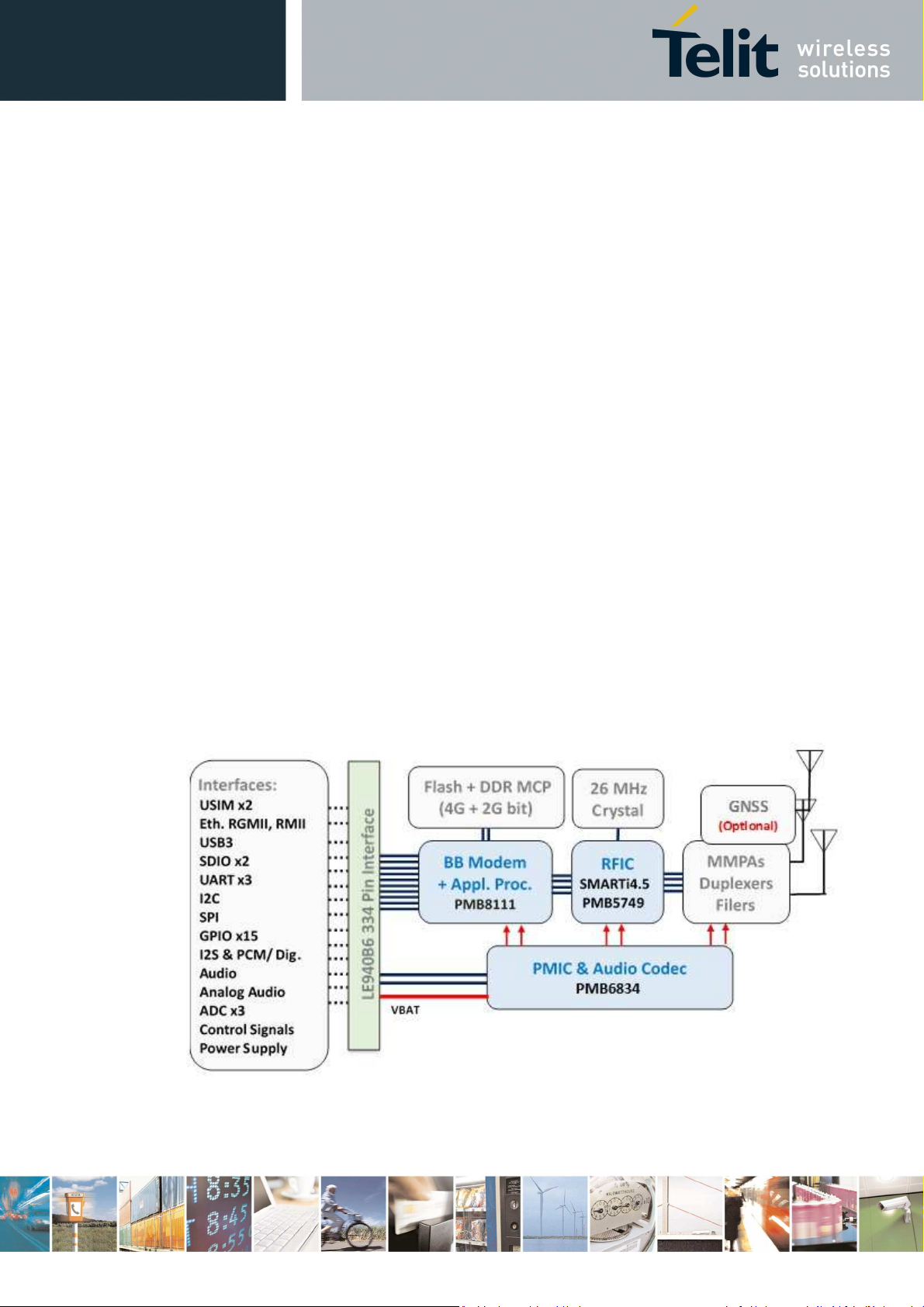
The LE940B6 family of automotive cellular modules features an LTE and multi-RAT modem
together with a powerful on-chip application processor and a rich set of interfaces.
The major functions and features are listed below:
• Multi-RAT with LTE carrier aggregation (Rel. 10, Cat. 6)
• Flash + DDR large enough to allow the space for customer’s own software applications
• Advanced security features
• FOTA (optional)
• Several region variants with optimal choice of RF bands in each for worldwide coverage of
countries and MNOs
• Well-designed form factor (40x40mm), accommodating the multiple RF bands in each region
variant
• Digital audio and analog audio codec
• A GNSS function is not included within the module, but can be supported with the proper
interface while mounted on the customer board
• The entire module is designed by Telit for satisfying the environment and quality
requirements of the automotive market
Figure 1 shows the high-level functionality of the LE940B6 module.
Figure 1: LE940B6 High-level Functionality
Reproduction forbidden without written authorization by Telit Communications S.p.A. - All Rights Reserved
Telit Confidential Information, provided under NDA Page
18 of 104

LE940B6 Hardware User Guide
1VV0301331 Rev. 1.8 - 2017-03-15
2.4. Environmental Requirements
2.4.1. Temperature Range
Operating
temperature range
Storage and nonoperating
temperature range
-20 ~ +55°C.
This range is defined by 3GPP (the global standard for wireless
mobile communication). Telit guarantees its modules to comply with
all the 3GPP requirements and to have full functionality of the
module with in this range.
-40 ~ +85°C.
Telit guarantees full functionality within this range as well. However,
there may possibly be some performance deviations in this
extended range relative to 3GPP requirements, which means that
some RF parameters may deviate from the 3GPP specification in the
order of a few dB. For example: receiver sensitivity or maximum
output power may be slightly degraded.
Even so, all the functionalities, such as call connection, SMS, USB
communication, UART activation etc., will be maintained, and the
effect of such degradations will not lead to malfunction.
–40°C ~ +95°C.
eCall must be functional (until the module is broken)
–40°C ~ +95°C
2.4.2. RoHS Compliance
As a part of the Telit corporate policy of environmental protection, the LE940B6 complies with the
RoHS (Restriction of Hazardous Substances) directive of the European Union (EU directive
2011/65/EU).
Reproduction forbidden without written authorization by Telit Communications S.p.A. - All Rights Reserved
Telit Confidential Information, provided under NDA Page
19 of 104
LE940B6 Hardware User Guide
1VV0301331 Rev. 1.8 - 2017-03-15
2.5. Operating Frequency Bands
The operating frequencies in WCDMA and LTE modes conform to the 3GPP specifications.
2.5.1. RF Bands per Regional Variant
Table 4 summarizes all region variants within the LE940B6 family, showing the supported band
sets in each variant and the supported band pairs for 2x carrier aggregation.
Table 4: RF Bands per Regional Variant
Region
LTE FDD LTE TDD HSPA+ TD-
Variant
LE940B6-NA
LE940B6-NV
LE940B6-RW
LE940B6-CN
2, 4, 5, 7, 12, 29(DL) - 2, 4, 5
LTE Carrier Aggregation 2+5, 2+12, 2+29, 4+4, 4+5, 4+12, 4+29
2, 4, 5, 7, 12, 13, 29(DL) - 2, 4, 5 - 2, 5
LTE Carrier Aggregation 2+5, 2+12, 2+13, 2+29, 4+4, 4+5, 4+12, 4+13, 4+29,
1, 2, 3, 4, 5, 7, 8, 19, 20,
21, 26, 28, 32(DL)
LTE Carrier Aggregation 1+5, 1+8, 1+19, 1+21, 1+26, 3+3, 3+5, 3+7, 3+19, 3+20,
1, 3, 5, 8, 26 38, 39, 40, 41M 1, 3, 5, 8 34, 39 3, 8
LTE Carrier Aggregation 1+26, 3+3, 3+5, 3+26, 39+41, 40+40, 41+41
Band 41M for China: 2,555 - 2,655 MHz
2G
SCDMA
- 1, 2, 3, 4, 5, 8, 19 - 2, 3, 5, 8
3+26, 3+28, 4+4, 7+20, 7+28, 19+21, 20+32
- 2, 5
Reproduction forbidden without written authorization by Telit Communications S.p.A. - All Rights Reserved
Telit Confidential Information, provided under NDA Page
20 of 104

LE940B6 Hardware User Guide
1VV0301331 Rev. 1.8 - 2017-03-15
2.5.2. Reference Table of RF Bands Characteristics
Table 5: RF Bands Characteristics
Mode Freq. Tx (MHz) Freq. Rx (MHz)
PCS 1900 1850.2 ~ 1909.8 1930.2 ~ 1989.8 512 ~ 810 80 MHz
DCS 1800 1710.2 ~ 1784.8 1805.2 ~ 1879.8 512 ~ 885 95 MHz
GSM 850 824.2 ~ 848.8 869.2 ~ 893.8 128 ~ 251 45 MHz
EGSM 900 880.2 ~ 914.8 925.2 ~ 959.8 975 ~ 1023, 1 ~ 124 45 MHz
WCDMA 2100 – B1 1920 ~ 1980 2110 ~ 2170 Tx: 9612 ~ 9888
WCDMA 1900 – B2 1850 ~ 1910 1930 ~ 1990 Tx: 9262 ~ 9538
WCDMA 1800 – B3 1710 ~ 1785 1805 ~ 1880 Tx: 937 ~ 1288
WCDMA AWS – B4 1710 ~ 1755 2110 ~ 2155 Tx: 1312 ~ 1513
Channels Tx-Rx Offset
190 MHz
Rx: 10562 ~ 10838
80 MHz
Rx: 9662 ~ 9938
95 MHz
Rx: 1162 ~ 1513
400 MHz
Rx: 1537 ~ 1738
WCDMA 850 – B5 824 ~ 849 869 ~ 894 Tx: 4132 ~ 4233
Rx: 4357 ~ 4458
WCDMA 900 – B8 880 ~ 915 925 ~ 960 Tx: 2712 ~ 2863
Rx: 2937 ~ 3088
WCDMA 1800 –B9 1750 ~ 1784.8 1845 ~ 1879.8 Tx: 8762 ~ 8912
Rx: 9237 ~ 9387
WCDMA 800 – B19 830 ~ 845 875 ~ 890 Tx: 312 ~ 363
Rx: 712 ~ 763
TDSCDMA 2000 –
B34
2010 ~ 2025 2010 ~ 2025 Tx: 10050 ~ 10125
Rx: 10050 ~ 10125
45 MHz
45 MHz
95 MHz
45 MHz
0 MHz
Reproduction forbidden without written authorization by Telit Communications S.p.A. - All Rights Reserved
Telit Confidential Information, provided under NDA Page
21 of 104
LE940B6 Hardware User Guide
1VV0301331 Rev. 1.8 - 2017-03-15
Mode Freq. Tx (MHz) Freq. Rx (MHz)
TDSCDMA 1900 –
B39
1880 ~ 1920 1880 ~ 1920 Tx: 9400 ~ 9600
Channels Tx-Rx Offset
Rx: 9400 ~ 9600
LTE 2100 – B1 1920 ~ 1980 2110 ~ 2170 Tx: 18000 ~ 18599
Rx: 0 ~ 599
LTE 1900 – B2 1850 ~ 1910 1930 ~ 1990 Tx: 18600 ~ 19199
Rx: 600 ~ 1199
LTE 1800 – B3 1710 ~ 1785 1805 ~ 1880 Tx: 19200 ~ 19949
Rx: 1200 ~ 1949
LTE AWS – B4 1710 ~ 1755 2110 ~ 2155 Tx: 19950 ~ 20399
Rx: 1950 ~ 2399
LTE 850 – B5 824 ~ 849 869 ~ 894 Tx: 20400 ~ 20649
Rx: 2400 ~ 2649
0 MHz
190 MHz
80 MHz
95 MHz
400 MHz
45 MHz
LTE 2600 – B7 2500 ~ 2570 2620 ~ 2690 Tx: 20750 ~ 21449
Rx: 2750 ~ 3449
LTE 900 – B8 880 ~ 915 925 ~ 960 Tx: 21450 ~ 21799
Rx: 3450 ~ 3799
LTE 1800 – B9 1749.9 ~ 1784.9 1844.9 ~ 1879.9 Tx: 21800 ~ 2149
Rx: 3800 ~ 4149
LTE AWS+ – B10 1710 ~ 1770 2110 ~ 2170 Tx: 22150 ~ 22749
Rx: 4150 ~ 4749
LTE 700a – B12 699 ~ 716 729 ~ 746 Tx : 23010 ~ 23179
Rx : 5010 ~ 5179
LTE 700c – B13 777 ~ 787 746 ~ 756 Tx : 23180 ~ 23279
Rx : 5180 ~ 5279
LTE 700b – B17 704 ~ 716 734 ~ 746 Tx: 23730 ~ 23849
120 MHz
45 MHz
95 MHz
400 MHz
30 MHz
-31 MHz
30 MHz
Rx: 5730 ~ 5849
Reproduction forbidden without written authorization by Telit Communications S.p.A. - All Rights Reserved
Telit Confidential Information, provided under NDA Page
22 of 104

LE940B6 Hardware User Guide
1VV0301331 Rev. 1.8 - 2017-03-15
Mode Freq. Tx (MHz) Freq. Rx (MHz)
LTE 800 – B19 830 ~ 845 875 ~ 890 Tx: 24000 ~ 24149
Channels Tx-Rx Offset
45 MHz
Rx: 6000 ~ 6149
LTE 800 – B20 832 ~ 862 791 ~ 821 Tx: 24150 ~ 24449
-41 MHz
Rx: 6150 ~ 6449
LTE 1500 – B21 1447.9 ~ 1462.9 1495.9 ~ 1510.9 Tx: 24450 ~ 24599
48 MHz
Rx: 6450 ~ 6599
LTE 850+ – B26 814 ~ 849 859 ~ 894 Tx: 26690 ~ 27039
45 MHz
Rx: 8690 ~ 9039
LTE 700 – B28 703 ~ 748 758 ~ 803 Tx : 27210 ~ 27659
45 MHz
Rx : 9210 ~ 9659
LTE 700d – B29 Downlink only 717 ~ 728 Rx: 9660 ~ 9769 0 MHz
LTE 1500 – B32 Downlink only 1452 ~ 1496 Rx: 9920 ~ 10359 0 MHz
LTE TDD 2600 – B38 2570 ~ 2620 2570 ~ 2620 Tx: 37750 ~ 38249
Rx: 37750 ~ 38249
LTE TDD 1900 – B39 1880 ~ 1920 1880 ~ 1920 Tx: 38250 ~ 38649
Rx: 38250 ~ 38649
LTE TDD 2300 – B40 2300 ~ 2400 2300 ~ 2400 Tx: 38650 ~ 39649
Rx: 38650 ~ 39649
LTE TDD 2500 – B41 2496 ~ 2690 2496 ~ 2690 Tx: 39650 ~ 41589
Rx: 39650 ~ 41589
0 MHz
0 MHz
0 MHz
0 MHz
Reproduction forbidden without written authorization by Telit Communications S.p.A. - All Rights Reserved
Telit Confidential Information, provided under NDA Page
23 of 104

LE940B6 Hardware User Guide
1VV0301331 Rev. 1.8 - 2017-03-15
2.6. Sensitivity
LE940B6 maximum sensitivity levels are as follows (exact performance figures will be specified at
a later stage):
• < 3GPP @ 2G
• < 3GPP @ 3G
• < 3GPP @ 4G FDD (BW=5 MHz)
• < 3GPP @ 4G TDD (BW=5 MHz)
Reproduction forbidden without written authorization by Telit Communications S.p.A. - All Rights Reserved
Telit Confidential Information, provided under NDA Page
24 of 104

LE940B6 Hardware User Guide
1VV0301331 Rev. 1.8 - 2017-03-15
2.7. LE940B6 Mechanical Specifications
2.7.1. Dimensions
The LE940B6 module’s overall dimensions are:
• Length: 40 mm, +/- 0.20 mm tolerance
• Width: 40 mm, +/- 0.20 mm tolerance
• Thickness: 3.0 mm, +/- 0.15 mm tolerance (with label)
2.7.2. Weight
The nominal weight of the LE940B6 module is 11 gram.
Reproduction forbidden without written authorization by Telit Communications S.p.A. - All Rights Reserved
Telit Confidential Information, provided under NDA Page
25 of 104

Power sense for the internal USB
Input for Request To Send signal
Output for Clear To Send signal
Output for Data Set Ready signal
Input for Data Terminal Ready
Output for
Data Carrier Detect
Output for Ring Indicator signal (RI)
Input for Request To Send (RTS)
Output for Clear To Send (CTS) to
LE940B6 Hardware User Guide
1VV0301331 Rev. 1.8 - 2017-03-15
3. LE940B6 Module Connections
3.1. Pin-out
Table 6: LE940B6 Pin-out
PAD Signal I/O
USB HS 2.0 Communication Port
A18 USB_VBUS AI
D19 USB_D+ I/O USB differential Data (+)
F19 USB_D- I/O USB differential Data (-)
AH19 C103/TXD I Serial data input (TXD) from DTE 1.8V
AF19 C104/RXD O Serial data output (RXD) to DTE 1.8V
AA18 C105/RTS I
AK19 C106/CTS O
AG18 C107/DSR O
AC18 C108/DTR I
AE18 C109/DCD O
AJ18 C125/RING O
AB19 TXD_AUX O Auxiliary UART (Tx Data to DTE) 1.8V
AD19 RXD_AUX I Auxiliary UART (Rx Data from DTE) 1.8V
AM9 UART3_TXD I Serial data input (TXD) from DTE 1.8V
AM11 UART3_RXD O Serial data output (RXD) to DTE 1.8V
transceiver
Asynchronous UART
(RTS) from DTE
(CTS) to DTE
(DSR) to DTE
signal (DTR) from DTE
signal (DCD) to DTE
to DTE
Asynchronous Auxiliary UART
Asynchronous UART3
Function Type COMMENT
1.8V
1.8V
1.8V
1.8V
1.8V
1.8V
AM13 UART3_RTS I
AM15 UART3_CTS O
E4 JTAG_TDI I JTAG_TDI 1.8V
F3 JTAG_RESOUT_N O JTAG_RESOUT* 1.8V
F5 JTAG_TRIGOUT - JTAG_TRIGOUT 1.8V
G2 JTAG_RTCK O JTAG_RTCK 1.8V
Reproduction forbidden without written authorization by Telit Communications S.p.A. - All Rights Reserved
Telit Confidential Information, provided under NDA Page
from DTE
DTE
JTAG – Joint Test Action Group
1.8V
1.8V
26 of 104

External SIM signal
– Power supply
External SIM signal
– Power supply
External SIM signal
– Presence
Digital Voice interface (CLK master
Digital Voice interface (WA0 master
LE940B6 Hardware User Guide
1VV0301331 Rev. 1.8 - 2017-03-15
H3 JTAG_TCK I JTAG_TCK 1.8V
J2 JTAG_TRST_N I JTAG_TRST* 1.8V
K3 JTAG_TDO O JTAG_TDO 1.8V
L2 JTAG_TMS I JTAG_TMS 1.8V
M3 JTAG_TRIGIN - JTAG_TRIGIN 1.8V
JTAG - MiPi 34 Interface
L4 JTAG_PTI_CLK O MiPi Clock 1.8V
N4 JTAG_PTI_DATA0 I/O MiPi Data 0 1.8V
R4 JTAG_PTI_DATA1 I/O MiPi Data 1 1.8V
T4 JTAG_PTI_DATA2 I/O MiPi Data 2 1.8V
V4 JTAG_PTI_DATA3 I/O MiPi Data 3 1.8V
SIM Card Interface
A8 SIMVCC1 -
for the SIM
A10 SIMCLK1 O External SIM signal – Clock 1.8/2.9V
1.8/2.9V
B7 SIMIN1 I External SIM signal – Presence 1.8V Active Low
B9 SIMIO1 I/O External SIM signal – Data I/O 1.8/2.9V
B11 SIMRST1 O External SIM signal – Reset 1.8/2.9V
SIM Card Interface 2
D15 SIMVCC2 -
for the SIM
C16 SIMCLK2 O External SIM signal – Clock 1.8/2.9V
C18 SIMIN2 I
(active low)
E16 SIMIO2 I/O External SIM signal – Data I/O 1.8/2.9V
D17 SIMRST2 O External SIM signal – Reset 1.8/2.9V
1.8/2.9V
1.8V Active Low
Analog Audio Interface
B5 EAR1_MT+ AO Earphone signal output, phase +
A4 EAR1_MT- AO Earphone signal output, phase -
B3 MIC1_MT+ AI Microphone input, phase +
A2 MIC1_MT- AI Microphone input, phase -
G6 MIC_BIAS AO Microphone Bias Power
Digital Voice Interface (DVI)
C8 DVI_RX I Digital Voice interface (Rx) 1.8V
C10 DVI_CLK O
D9 DVI_TX O Digital Voice interface (Tx) 1.8V
D11 DVI_WA0 O
K19 SPI_MOSI O SPI data Master output Slave input 1.8V
M19 SPI_MISO I SPI data Master input Slave output 1.8V
Reproduction forbidden without written authorization by Telit Communications S.p.A. - All Rights Reserved
Telit Confidential Information, provided under NDA Page
output)
output)
SPI – Serial Peripheral Interface
1.8V
1.8V
27 of 104

RGMII Transmit Enable / Error or
LE940B6 Hardware User Guide
1VV0301331 Rev. 1.8 - 2017-03-15
N18 SPI_CS O SPI Chip select output 1.8V
P19 SPI_CLK O SPI Clock output 1.8V
I2C Interface
C14 I2C_SCL I/O I2C Clock 1.8V
D13 I2C_SDA I/O I2C Data 1.8V
Digital I/O
F9 GPIO_01 I/O GPIO_01 1.8V
E10 GPIO_02 I/O GPIO_02 1.8V
F11 GPIO_03 I/O GPIO_03 1.8V
E12 GPIO_04 I/O GPIO_04 1.8V
F13 GPIO_05 I/O GPIO_05 1.8V
E14 GPIO_06 I/O GPIO_06 1.8V
R18 GPIO_07 I/O GPIO_07 1.8V
S19 GPIO_08 I/O GPIO_08 1.8V
U19 GPIO_09 I/O GPIO_09 1.8V
W19 GPIO_10 I/O GPIO_10 1.8V
L18 GPIO_11 I/O GPIO_11 1.8V
J18 GPIO_12 I/O GPIO_12 1.8V
AN4 GPIO_20 I/O GPIO_20 1.8V
H1 GPIO_21 I/O GPIO_21 1.8V
K1 GPIO_22 I/O GPIO_22 1.8V
Analog to Digital Converter
D5 ADC_IN1 AI Analog to Digital Converter Input 1 Analog
E6 ADC_IN2 AI Analog to Digital Converter Input 2 Analog
F7 ADC_IN3 AI Analog to Digital Converter Input 3 Analog
Ethernet MAC/PHY Signals
G14 MAC_MDC O Management Data Clock 2.5/3.3V
G12 MAC_MDIO I/O Management Data I/O 2.5/3.3V
V16 MAC_TXD[0] O RGMII or RMII TXD[0] 2.5/3.3V
T16 MAC_TXD[1] O RGMII or RMII TXD[1] 2.5/3.3V
R16 MAC_TXD[2] O RGMII TXD[2] 2.5/3.3V
N16 MAC_TXD[3] O RGMII TXD[3] 2.5/3.3V
L16 MAC_GTX_CLK O RGMII Transmit Clock 2.5/3.3V
G16 MAC_TXEN_ER O
AL16 MAC_RXD[0] I RGMII or RMII RXD[0] 2.5/3.3V
AJ16 MAC_RXD[1] I RGMII or RMII RXD[1] 2.5/3.3V
AG16 MAC_RXD[2] I RGMII RXD[2] 2.5/3.3V
AE16 MAC_RXD[3] I RGMII RXD[3] 2.5/3.3V
AC16 MAC_RX_CLK I RGMII Receive Clock 2.5/3.3V
Reproduction forbidden without written authorization by Telit Communications S.p.A. - All Rights Reserved
Telit Confidential Information, provided under NDA Page
RMII Transmit Enable
2.5/3.3V
28 of 104
RGMII Receive Data Available/Error
Indicates that the boot sequence
Supply output for external
Main Power Supply (RF Transmit
Ma
in Power Supply (RF Transmit
Main Power Supply (RF Transmit
Main Power Supply (RF Transmit
Main Power Supply (RF Transmit
Main Power Supply (RF Transmit
LE940B6 Hardware User Guide
1VV0301331 Rev. 1.8 - 2017-03-15
X16 MAC_RXDV_ER I
or RMII Receive Error
G10 ETH_INT_N I Ethernet PHY Interrupt 2.5/3.3V
G8 ETH_RST_N O Ethernet PHY Reset Output 2.5/3.3V
2.5/3.3V
RF Section
AD1 ANT_1 I/O Primary Antenna 1 RF
AU9 ANT_DIV_1 I Diversity Antenna 1 RF
S1 ANT_GPS I GPS Antenna RF
Miscellaneous Functions
F17 VRTC AI VRTC Backup capacitor -
K17 VIO_1.8V O VIO_1.8V for reference voltage 1.8V
AN8 RESET_N I Reset Input Active low
AN10 SW_RDY O
completed successfully
1.8V
AN12 SHDN_N I Unconditional Shutdown Input Active low
AS1 ON_OFF_N I Power ON/OFF Input Active low
AU3 STAT_LED O Status Indicator LED 1.8V
P17 VAUX/PWRMON O
accessories / Power ON Monitor
1.8V
H17 VPP I Vpp for eFuse
Power Supply
AP17 VBATT - Main Power Supply (Digital Section) Power
AP19 VBATT - Main Power Supply (Digital Section) Power
AR18 VBATT - Main Power Supply (Digital Section) Power
AR20 VBATT - Main Power Supply (Digital Section) Power
AS17 VBATT_PA -
AS19 VBATT_PA -
AT18 VBATT_PA -
AU17 VBATT_PA -
AU19 VBATT_PA -
AT20 VBATT_PA -
Power Section)
Power Section)
Power Section)
Power Section)
Power Section)
Power Section)
Power
Power
Power
Power
Power
Power
Ground
A6 GND - Ground Ground
A12 GND - Ground Ground
B13 GND - Ground Ground
B15 GND - Ground Ground
Reproduction forbidden without written authorization by Telit Communications S.p.A. - All Rights Reserved
Telit Confidential Information, provided under NDA Page
29 of 104

LE940B6 Hardware User Guide
1VV0301331 Rev. 1.8 - 2017-03-15
B17 GND - Ground Ground
C4 GND - Ground Ground
C6 GND - Ground Ground
D3 GND - Ground Ground
D7 GND - Ground Ground
E18 GND - Ground Ground
F1 GND - Ground Ground
G18 GND - Ground Ground
H19 GND - Ground Ground
M1 GND - Ground Ground
N2 GND - Ground Ground
P1 GND - Ground Ground
P3 GND - Ground Ground
R2 GND - Ground Ground
T2 GND - Ground Ground
T18 GND - Ground Ground
U1 GND - Ground Ground
V18 GND - Ground Ground
W1 GND - Ground Ground
X2 GND - Ground Ground
X18 GND - Ground Ground
Y1 GND - Ground Ground
Y19 GND - Ground Ground
AA2 GND - Ground Ground
AB1 GND - Ground Ground
AC2 GND - Ground Ground
AE2 GND - Ground Ground
AF1 GND - Ground Ground
AG2 GND - Ground Ground
AH1 GND - Ground Ground
AJ2 GND - Ground Ground
AK1 GND - Ground Ground
AK17 GND - Ground Ground
AL18 GND - Ground Ground
AM17 GND - Ground Ground
AM19 GND - Ground Ground
AN16 GND - Ground Ground
AN18 GND - Ground Ground
AP3 GND - Ground Ground
AP5 GND - Ground Ground
Reproduction forbidden without written authorization by Telit Communications S.p.A. - All Rights Reserved
Telit Confidential Information, provided under NDA Page
30 of 104
 Loading...