

Telit Communications S p A LE920NA User Manual

L
LE920
Hardware User Guide
(Preliminary)
H
1vv0301026 Rev.0 - draft4 – 2013-05-21 (

LE920 Hardware User Guide
1vv0301026 Rev.0 - draft4 – 2013-05-
APPLICABILITY TABLE
PRODUCT
LE920--EU
LE920--NA
L
Reproduction forbidden without written authorization from Telit Communications S.p.A. - All Rights Reserved. Page 2 of 76

L
LE920 Hardware User Guide
1vv0301026 Rev.0 - draft4 – 2013-05-
SPECIFICATIONS SUBJECT TO CHANGE WITHOUT NOTICE
Notice
While reasonable efforts have been made to assure the accuracy of this document, Telit
assumes no liability resulting from any inaccuracies or omissions in this document, or from
use of the information obtained herein. The information in this document has been carefully
checked and is believed to be entirely reliable. However, no responsibility is assumed for
inaccuracies or omissions. Telit reserves the right to make changes to any products described
herein and reserves the right to revise this document and to make changes from time to time
in content hereof with no obligation to notify any person of revisions or changes. Telit does
not assume any liability arising out of the application or use of any product, software, or
circuit described herein; neither does it convey license under its patent rights or the rights of
others.
It is possible that this publication may contain references to, or information about Telit
products (machines and programs), programming, or services that are not announced in your
country. Such references or information must not be construed to mean that Telit intends to
announce such Telit products, programming, or services in your country.
Copyrights
This instruction manual and the Telit products described in this instruction manual may be,
include or describe copyrighted Telit material, such as computer programs stored in
semiconductor memories or other media. Laws in the Italy and other countries preserve for
Telit and its licensors certain exclusive rights for copyrighted material, including the
exclusive right to copy, reproduce in any form, distribute and make derivative works of the
copyrighted material. Accordingly, any copyrighted material of Telit and its licensors
contained herein or in the Telit products described in this instruction manual may not be
copied, reproduced, distributed, merged or modified in any manner without the express
written permission of Telit. Furthermore, the purchase of Telit products shall not be deemed
to grant either directly or by implication, estoppel, or otherwise, any license under the
copyrights, patents or patent applications of Telit, as arises by operation of law in the sale of a
product.
Computer Software Copyrights
The Telit and 3rd Party supplied Software (SW) products described in this instruction manual
may include copyrighted Telit and other 3rd Party supplied computer programs stored in
semiconductor memories or other media. Laws in the Italy and other countries preserve for
Telit and other 3rd Party supplied SW certain exclusive rights for copyrighted computer
programs, including the exclusive right to copy or reproduce in any form the copyrighted
computer program. Accordingly, any copyrighted Telit or other 3rd Party supplied SW
computer programs contained in the Telit products described in this instruction manual may
not be copied (reverse engineered) or reproduced in any manner without the express written
permission of Telit or the 3rd Party SW supplier. Furthermore, the purchase of Telit products
shall not be deemed to grant either directly or by implication, estoppel, or otherwise, any
license under the copyrights, patents or patent applications of Telit or other 3rd Party supplied
SW, except for the normal non-exclusive, royalty free license to use that arises by operation
of law in the sale of a product.
Reproduction forbidden without written authorization from Telit Communications S.p.A. - All Rights Reserved. Page 3 of 76

L
LE920 Hardware User Guide
1vv0301026 Rev.0 - draft4 – 2013-05-
Usage and Disclosure Restrictions
License Agreements
The software described in this document is the property of Telit and its licensors. It is
furnished by express license agreement only and may be used only in accordance with the
terms of such an agreement.
Copyrighted Materials
Software and documentation are copyrighted materials. Making unauthorized copies is
prohibited by law. No part of the software or documentation may be reproduced, transmitted,
transcribed, stored in a retrieval system, or translated into any language or computer language,
in any form or by any means, without prior written permission of Telit
High Risk Materials
Components, units, or third-party products used in the product described herein are NOT
fault-tolerant and are NOT designed, manufactured, or intended for use as on-line control
equipment in the following hazardous environments requiring fail-safe controls: the operation
of Nuclear Facilities, Aircraft Navigation or Aircraft Communication Systems, Air Traffic
Control, Life Support, or Weapons Systems (High Risk Activities"). Telit and its supplier(s)
specifically disclaim any expressed or implied warranty of fitness for such High Risk
Activities.
Trademarks
TELIT and the Stylized T Logo are registered in Trademark Office. All other product or
service names are the property of their respective owners.
Copyright © Telit Communications S.p.A. 2012.
Reproduction forbidden without written authorization from Telit Communications S.p.A. - All Rights Reserved. Page 4 of 76

LE920 Hardware User Guide
Contents
1. Introduction ........................................................................................................... 9
2. General Product Description ................................................................................ 12
2.5.1.1.
2.5.1.2.
2.5.1.3.
2.5.1.4.
2.5.1.5.
2.5.1.6.
2.5.1.7.
3. LE920 Module Connections .................................................................................. 17
4. Hardware Commands .......................................................................................... 25
L
1vv0301026 Rev.0 - draft4 – 2013-05-
1.1. Scope ............................................................................................................................ 9
1.2. Audience ....................................................................................................................... 9
1.3. Contact Information, Support ...................................................................................... 9
1.4. Document Organization ............................................................................................. 10
1.5. Text Conventions ........................................................................................................ 11
1.6. Related Documents ................................................................................................... 11
2.1. Overview ..................................................................................................................... 12
2.2. LE920 Mechanical Dimensions .................................................................................. 13
2.3. Weight ........................................................................................................................ 13
2.4. Environmental requirements .................................................................................... 14
2.4.1. Temperature range ........................................................................................................ 14
2.4.2. RoHS compliance ........................................................................................................... 14
2.5. Operating Frequency ................................................................................................. 15
WCDMA1700 – B4 .................................................................................................. 15
(LE920-NA only) ...................................................................................................... 15
1710 ~ 1755 .............................................................................................................. 15
2110 ~ 2155 .............................................................................................................. 15
Tx: 1312 ~ 1513 ........................................................................................................ 15
Rx: 9662 ~ 9938 ....................................................................................................... 15
400 MHz .................................................................................................................. 15
3.1. PIN-OUT ..................................................................................................................... 17
3.1.1. LGA Pads Layout ............................................................................................................ 24
4.1. Turning ON the LE920 ................................................................................................ 25
4.2. Initialization and Activation state ............................................................................... 25
4.3. Turning OFF the LE920 .............................................................................................. 27
4.3.1. Shutdown by Software Command .................................................................................. 28
Reproduction forbidden without written authorization from Telit Communications S.p.A. - All Rights Reserved. Page 5 of 76

L
LE920 Hardware User Guide
5. Power Supply ....................................................................................................... 33
6. Antenna(s) ........................................................................................................... 42
7. Logic Level Specifications .................................................................................... 48
8. USB Port .............................................................................................................. 49
9. Serial Ports .......................................................................................................... 50
10. Audio Section Overview ..................................................................................... 54
1vv0301026 Rev.0 - draft4 – 2013-05-
4.3.2. Hardware Shutdown ...................................................................................................... 29
4.3.3. Hardware Unconditional Restart ................................................................................... 30
4.3.4. Hardware Unconditional Shutdown ............................................................................... 31
4.4. Summary of Turning ON and OFF the module .......................................................... 32
5.1. Power Supply Requirements ..................................................................................... 33
5.2. General Design Rules ................................................................................................ 35
5.2.1. Electrical Design Guidelines .......................................................................................... 35
5.2.1.1. + 5V Input Source Power Supply Design Guidelines .............................................. 35
5.2.1.2. + 12V Input Source Power Supply Design Guidelines............................................. 36
5.2.1.3. Battery Source Power Supply Design Guidelines ................................................... 38
5.2.2. Thermal Design Guidelines............................................................................................ 39
5.2.3. Power Supply PCB Layout Guidelines ........................................................................... 40
6.1. GSM/WCDMA/LTE Antenna Requirements ............................................................... 42
6.2. GSM/WCDMA/LTE Antenna – PCB line Guidelines ................................................... 43
6.3. GSM/WCDMA/LTE Antenna – Installation Guidelines ............................................... 44
6.4. Antenna Diversity Requirements............................................................................... 44
6.5. GPS/GNSS Antenna Requirements ........................................................................... 45
6.5.1. Combined GPS/GNSS Antenna ...................................................................................... 45
6.5.2. Linear and Patch GPS/GNSS Antenna ........................................................................... 46
6.5.3. Front End Design Considerations .................................................................................. 46
6.5.4. GPS/GNSS Antenna - PCB Line Guidelines ................................................................... 46
6.5.5. GPS/GNSS Antenna – Installation Guidelines ............................................................... 47
9.1. Modem Serial Port 1 .................................................................................................. 51
9.2. Modem Serial Port 2 .................................................................................................. 52
9.3. RS232 Level Translation ............................................................................................ 52
Reproduction forbidden without written authorization from Telit Communications S.p.A. - All Rights Reserved. Page 6 of 76

L
LE920 Hardware User Guide
11. General Purpose I/O .......................................................................................... 56
12. ADC section ...................................................................................................... 61
13. Mounting the module on your board .................................................................. 62
14. Application guide .............................................................................................. 68
1vv0301026 Rev.0 - draft4 – 2013-05-
10.1. Digital Audio ........................................................................................................... 54
11.1. Logic Level Specifications ...................................................................................... 57
11.2. Using a GPIO Pad as Input ...................................................................................... 57
11.3. Using a GPIO Pad as Output ................................................................................... 58
11.4. Using the Temperature Monitor Function ............................................................. 59
11.4.1. Short Description ........................................................................................................... 59
11.5. Indication of Network Service Availability .............................................................. 59
11.6. RTC Bypass Out ...................................................................................................... 60
11.7. VAUX Power Output ................................................................................................ 60
12.1. ADC Converter ........................................................................................................ 61
12.1.1. Description ..................................................................................................................... 61
12.1.2. Using ADC Converter ..................................................................................................... 61
13.1. General ................................................................................................................... 62
13.2. Finishing & Dimensions ......................................................................................... 62
13.3. Recommended foot print for the application ......................................................... 63
13.4. Stencil ..................................................................................................................... 64
13.5. PCB Pad Design ...................................................................................................... 64
13.6. Recommendations for PCB Pad Dimensions (mm)............................................... 64
13.7. Solder Paste ........................................................................................................... 66
13.7.1. Solder Reflow ................................................................................................................. 66
14.1. Debug of the LE920 in production .......................................................................... 68
14.2. Bypass capacitor on Power supplies ..................................................................... 69
14.3. SIM interface........................................................................................................... 69
14.4. EMC recommendations (TBD) ................................................................................ 70
14.5. Download and Debug Port ...................................................................................... 71
Reproduction forbidden without written authorization from Telit Communications S.p.A. - All Rights Reserved. Page 7 of 76

L
LE920 Hardware User Guide
15. Packing system ................................................................................................. 72
16. Safety Recommendations .................................................................................. 75
17. Document History ............................................................................................. 76
1vv0301026 Rev.0 - draft4 – 2013-05-
15.1. Tray Drawing........................................................................................................... 73
15.2. Moisture Sensibility ................................................................................................ 74
Reproduction forbidden without written authorization from Telit Communications S.p.A. - All Rights Reserved. Page 8 of 76
LE920 Hardware User Guide
1.
Introduction
1.1.
Scope
1.2.
Audience
1.3.
Contact Information, Support
The aim of this document is the description of some hardware solutions useful for developing
a product with the Telit LE920-EU/NA module. All the features and solutions detailed are
applicable to all LE920, whereas “LE920” is intended the modules listed in the applicability
table.
When a specific feature is applicable to a specific product, it will be clearly highlighted.
This document is intended for Telit customers, who are integrators, about to implement their
applications using our LE920
module.
L
1vv0301026 Rev.0 - draft4 – 2013-05-
For general contact, technical support, to report documentation errors and to order manuals,
contact Telit’s Technical Support Center (TTSC) at:
TS-EMEA@telit.com
TS-NORTHAMERICA@telit.com
TS-LATINAMERICA@telit.com
TS-APAC@telit.com
Alternatively, use:
http://www.telit.com/en/products/technical-support-center/contact.php
For detailed information about where you can buy the Telit modules or for recommendations
on accessories and components visit:
http://www.telit.com
To register for product news and announcements or for product questions contact Telit’s
Technical Support Center (TTSC).
Our aim is to make this guide as helpful as possible. Keep us informed of your comments and
suggestions for improvements.
Telit appreciates feedback from the users of our information.
Reproduction forbidden without written authorization from Telit Communications S.p.A. - All Rights Reserved. Page 9 of 76

LE920 Hardware User Guide
1.4.
Document Organization
L
1vv0301026 Rev.0 - draft4 – 2013-05-
This document contains the following chapters:
Chapter 1: “Introduction”
support information, and text conventions.
Chapter 2: “General Product Description”
Chapter 3: “LE920 Module Connections”
Chapter 4: “Hardware Commands”
Chapter 5: “Power Supply”
Chapter 6: “Antenna”
parts in the full product design
Chapter 7: “Logic Level specifications”
logic levels for this module.
Chapter 8: “USB Port”
Chapter 9: “Serial Ports”
Chapter 10: “Audio Section Overview”
Chapter 11: “General Purpose I/O”
Chapter 12 “DAC and ADC Section”
Chapter 13: “Mounting the module on your board”
Chapter 14: “Application Guides”
Chapter 15: “Packing System”
Chapter 16: “Conformity Assessments”
Chapter 17: “Safety Recommendations”
Chapter 18: “Document History”
provides a scope for this document, target audience, contact and
gives an overview of the features of the product.
deals with the pin out configuration and layout.
How to control the module via hardware
deals on supply and consumption.
The antenna connection and board layout design are the most important
Specific values adopted in the implementation of
How the general purpose I/O pads can be configured.
Deals with these two kind of converters.
Reproduction forbidden without written authorization from Telit Communications S.p.A. - All Rights Reserved. Page 10 of 76

LE920 Hardware User Guide
1.5.
Text Conventions
1.6.
Related Documents
L
1vv0301026 Rev.0 - draft4 – 2013-05-
Danger – This information MUST be followed or catastrophic equipment failure or bodily
injury may occur.
Caution or Warning – Alerts the user to important points about integrating the module, if
these points are not followed, the module and end user equipment may fail or malfunction.
Tip or Information – Provides advice and suggestions that may be useful when
integrating the module.
All dates are in ISO 8601 format, i.e. YYYY-MM-DD.
x LE920-EU/NA Product Description, 80407ST10118A
x LE920-EU/NA AT command reference guide, 80407ST10116A
x Telit EVK2 User Guide, 1vv0300704
Reproduction forbidden without written authorization from Telit Communications S.p.A. - All Rights Reserved. Page 11 of 76
LE920 Hardware User Guide
2.
General Product Description
2.1.
Overview
The aim of this document is the description of some hardware solutions useful for developing
a product with the Telit LE920 module.
In this document all the basic functions of a mobile phone will be taken into account; for each
one of them a proper hardware solution will be suggested and eventually the wrong solutions
and common errors to be avoided will be evidenced. Obviously this document cannot
embrace the whole hardware solutions and products that may be designed. The wrong
solutions to be avoided must be considered as mandatory, while the suggested hardware
configurations must not be considered mandatory, instead the information given must be used
as a guide and a starting point for properly developing your product with the Telit LE920
module.
L
1vv0301026 Rev.0 - draft4 – 2013-05-
.
NOTICE:
The integration of the GSM/GPRS/EGPRS/WCDMA/HSPA+/LTE LE920 cellular module
within user application must be done according to the design rules described in this manual.
The information presented in this document is believed to be accurate and reliable. However,
no responsibility is assumed by Telit Communication S.p.A. for its use, such as any
infringement of patents or other rights of third parties which may result from its use. No
license is granted by implication or otherwise under any patent rights of Telit Communication
S.p.A. other than for circuitry embodied in Telit products. This document is subject to change
without notice.
Reproduction forbidden without written authorization from Telit Communications S.p.A. - All Rights Reserved. Page 12 of 76

LE920 Hardware User Guide
2.2.
LE920 Mechanical Dimensions
2.3.
Weight
L
1vv0301026 Rev.0 - draft4 – 2013-05-
The Telit LE920 module overall dimensions are:
Length: 34 mm
Width: 40 mm
Thickness: 2.9 mm
The module weight of LE920-EU/NA is about 9.0 gram.
Reproduction forbidden without written authorization from Telit Communications S.p.A. - All Rights Reserved. Page 13 of 76
LE920 Hardware User Guide
2.4.
Environmental requirements
2.4.1.
Temperature range
2.4.2.
RoHS compliance
L
1vv0301026 Rev.0 - draft4 – 2013-05-
Note
–20°C ~ +55°C The module is fully functional (*) in all the
temperature range, and it fully meets the ETSI
specifications.
Operating Temperature
Range
Storage and non-operating
Temperature Range
(*)Functional: the module is able to make and receive voice calls, data calls and SMS.
As a part of Telit corporate policy of environmental protection, the LE920 complies with the
RoHS (Restriction of Hazardous Substances) directive of the European Union (EU directive
2002/95/EG).
–40°C ~ +85°C The module is fully functional (*) in all the
temperature range. Temperatures outside of
the range –20°C ÷ +55°C might slightly
deviate from ETSI specifications.
–40°C ~ +85°C
Reproduction forbidden without written authorization from Telit Communications S.p.A. - All Rights Reserved. Page 14 of 76
L
LE920 Hardware User Guide
2.5.
Operating Frequency
1vv0301026 Rev.0 - draft4 – 2013-05-
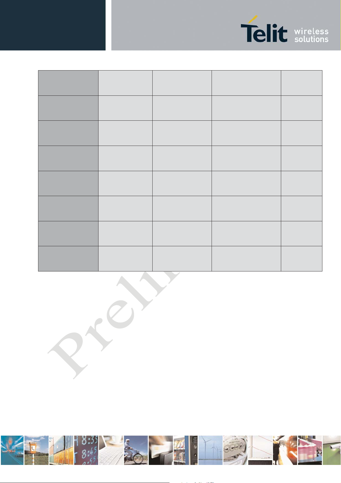
Mode Freq. TX (MHz) Freq. RX (MHz) Channels TX - RX
GSM850 824 ~ 849 869 ~ 894 128 ~ 251 45 MHz
EGSM900
DCS1800 1710 ~ 1785 1805 ~ 1880 512 ~ 885 95MHz
PCS1900 1850 ~ 1910 1930 ~ 1990 512 ~ 810 80MHz
The operating frequencies in GSM850, EGSM900, DCS1800, PCS1900, WCDMA & LTE
modes are conformed to the 3GPP specifications.
offset
890 ~ 915 935 ~ 960 0 ~ 124 45 MHz
880 ~ 890 925 ~ 935 975 ~ 1023 45 MHz
WCDMA2100 – B1
(LE920 both models)
WCDMA1900 – B2
(LE920-NA only)
WCDMA1800 – B3
(LE920-EU only)
WCDMA1700 – B4
(LE920-NA only)
WCDMA850 – B5
(LE920-NA only)
WCDMA800 – B6
(LE920-NA only)
WCDMA900 – B8
(LE920-EU only)
Tx: 9612 ~ 9888
1920 ~ 1980 2110 ~ 2170
1850 ~ 1910 1930 ~ 1990
1710 ~ 1785 1805 ~ 1880 Tx: 937 ~ 1288
1710 ~ 1755 2110 ~ 2155
824 ~ 849 869 ~ 894
830 ~ 840 875 ~ 885
880 ~ 915 925 ~ 960
Rx: 10562 ~ 10838
Tx: 9262 ~ 9538
Rx: 9662 ~ 9938
Rx: 1162 ~ 1513
Tx: 1312 ~ 1513
Rx: 9662 ~ 9938
Tx: 4132 ~ 4233
Rx: 4357 ~ 4458
Tx: 4162 ~ 4188
Rx: 4387 ~ 4413
Tx: 2712 ~ 2863
Rx: 2937 ~ 3088
190MHz
80MHz
95MHz
400 MHz
45MHz
45MHz
45MHz
LTE2100 – B1
1920 ~ 1980 2110 ~ 2170
(LE920 both models)
Reproduction forbidden without written authorization from Telit Communications S.p.A. - All Rights Reserved. Page 15 of 76
Tx: 18000 ~ 18599
190MHz
Rx: 0 ~ 599
L
LE920 Hardware User Guide
1vv0301026 Rev.0 - draft4 – 2013-05-
LTE1900 – B2
(LE920-NA only)
LTE1800 – B3
(LE920-EU only)
LTE1700 – B4
(LE920-NA only)
LTE850 – B5
(LE920-NA only)
LTE2600 – B7
(LE920-EU only)
LTE900 – B8
(LE920-EU only)
LTE700 – B17
(LE920-NA only)
1850 ~ 1910 1930 ~ 1990
Tx: 18600 ~ 19199
Rx: 600 ~ 1199
1710 ~ 1785 1805 ~ 1880 Tx: 19200 ~ 19949
Rx: 1200 ~ 1949
Tx: 19950 ~ 20399
1710~ 1755 2110 ~ 2155
Rx: 1950 ~ 2399
Tx: 20400 ~ 20649
824 ~ 849 869 ~ 894
Rx: 2400 ~ 2649
Tx: 20750 ~ 21449
2500 ~ 2570 2620 ~ 2690
Rx: 2750 ~ 3449
Tx: 21450 ~ 21799
880 ~ 915 925 ~ 960
Rx: 3450 ~ 3799
Tx: 23730 ~ 23849
704 ~ 716 734 ~ 746
Rx: 5730 ~ 5849
80MHz
95MHz
400MHz
45MHz
120MHz
45MHz
30MHz
LTE800 – B20
(LE920-EU only)
832 ~ 862 791 ~ 821
Tx: 24150 ~ 24449
-41MHz
Rx: 6150 ~ 6449
Reproduction forbidden without written authorization from Telit Communications S.p.A. - All Rights Reserved. Page 16 of 76
L
LE920 Hardware User Guide
3.
LE920 Module Connections
3.1.
PIN-OUT
1vv0301026 Rev.0 - draft4 – 2013-05-
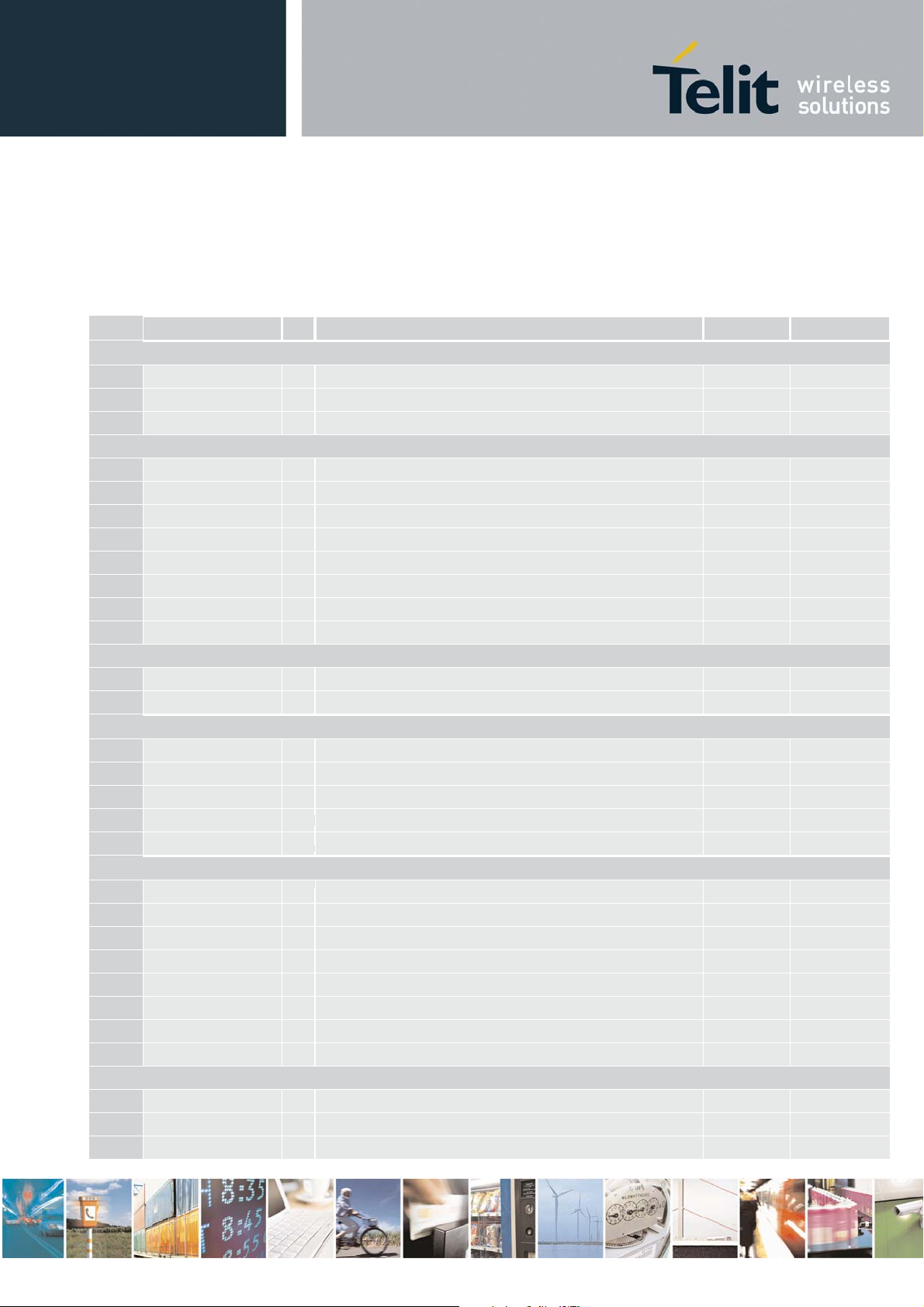
PAD Signal I/O Function Type COMMENT
USB HS 2.0 Communication Port
D19
F19
A18
Asynchronous UART – Prog. / data +HW Flow Control
AH19
AF19
AC18
AA18
AK19
AE18
AG18
AJ18
Asynchronous Auxiliary UART
AB19
AD19
SIM Card Interface 1
A10
B11
B9
B7
A8
Audio
B5
A4
B3
A2
E2
D1
C2
B1
Digital Voice interface (DVI)
D11
C8
D9
USB_D+ I/O USB differential Data(+)
USB_D- I/O USB differential Data(+)
USB_VBUS AI Power sense for the internal USB transceiver Power
C103/TXD I Serial data input (TXD) from DTE 1.8V
C104/RXD O Serial data output to DTE 1.8V
C108/DTR I Input for Data terminal ready signal (DTR) from DTE 1.8V
C105/RTS I Input for Request to send signal (RTS) from DTE 1.8V
C106/CTS O Output for Clear to send signal (CTS) to DTE 1.8V
C109/DCD O Output for Data carrier detect signal (DCD) to DTE 1.8V
C107/DSR O Output for Data set ready signal (DSR) to DTE 1.8V
C125/RING O Output for Ring indicator signal (RI) to DTE 1.8V
TXD_AUX O Auxillary UART (TX Data to DTE) 1.8V
RXD_AUX I Auxillary UART (RX Data from DTE) 1.8V
SIMCLK1 O External SIM signal – Clock 1.8/2.85V
SIMRST1 O External SIM signal – Reset 1.8/2.85V
SIMIO1 I/O External SIM signal - Data I/O 1.8/2.85V
SIMIN1 I External SIM signal - Presence (active low) 1.8V
SIMVCC1 - External SIM signal – Power supply for the SIM 1.8/2.85V
EAR1_MT+ AO Earphone signal output1, phase + Audio
EAR1_MT- AO Earphone signal output1, phase - Audio
MIC1_MT+ AI Mic signal input1, phase + Audio
MIC1_MT- AI Mic signal input1, phase - Audio
EAR2_MT+ AO Earphone signal output2, phase + Audio
EAR2_MT- AO Earphone signal output2, phase - Audio
MIC2_MT+ AI Mic signal input2, phase + Audio
MIC2_MT- AI Mic signal input2, phase - Audio
DVI_WA0 O Digital Voice interface (WA0 master output) 1.8V
DVI_RX I Digital Voice interface (RX) 1.8V
DVI_TX O Digital Voice interface (TX) 1.8V
Reproduction forbidden without written authorization from Telit Communications S.p.A. - All Rights Reserved. Page 17 of 76

L
LE920 Hardware User Guide
1vv0301026 Rev.0 - draft4 – 2013-05-
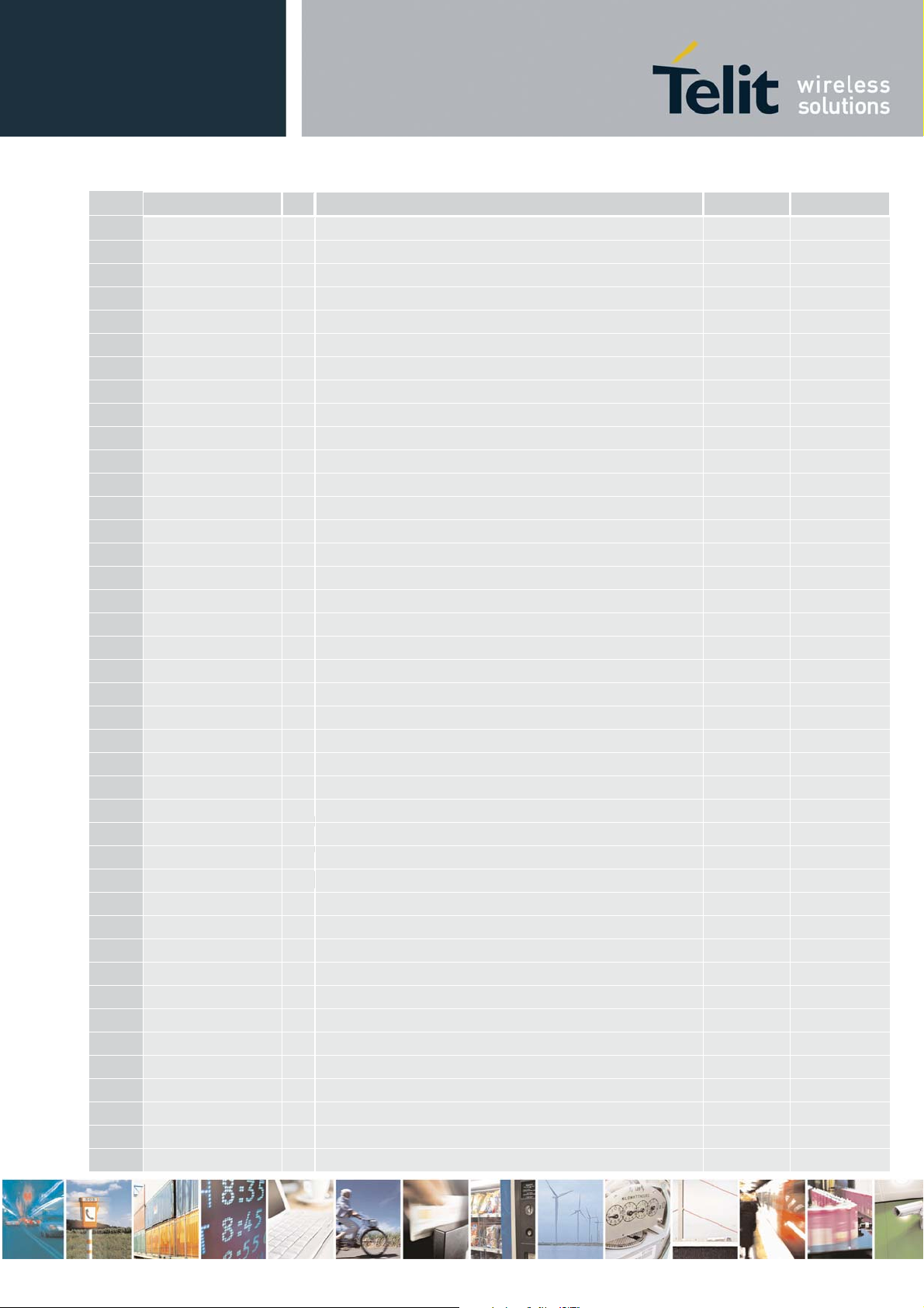
PAD Signal I/O Function Type COMMENT
C10
DVI_CLK O Digital Voice interface (CLK master output) 1.8V
Digital I/O
F9
E10
F11
E12
F13
E14
R18
S19
U19
W19
GPIO_01
GPIO_02
GPIO_03
GPIO_04
GPIO_05
GPIO_06
GPIO_07
GPIO_08
GPIO_09
GPIO_10
I/O
I/O
I/O
I/O
I/O
I/O
I/O
I/O
I/O
I/O
GPIO_01
GPIO_02
GPIO_03
GPIO_04
GPIO_05
GPIO_06
GPIO_07
GPIO_08
GPIO_09
GPIO_10
1.8V
1.8V
1.8V
1.8V
1.8V
1.8V
1.8V
1.8V
1.8V
1.8V
RF Section
AD1
AU9
Antenna I/O GSM/EDGE/UMTS/LTE Antenna (50 Ohm) RF
ANT_DIV I UMTS/LTE Antenna Diversity Input (50 Ohm) RF
GPS Section
S1
ANT_GPS I GPS Antenna (50 Ohm) RF
Miscellaneous Function
AP1
AS1
AN12
RESET# I Reset Input Active Low
ON_OFF# I Input Command for Power ON Active Low
SHDN_N I Unconditional Shut down Input Active Low
To be used to
F17
VRTC AI VRTC Backup Capacitor Power
back up the
RTC section
P17
D5
E6
F7
AU3
AN10
VAUX/PWRMON O
ADC_IN1 AI Analog/Digital Converter Input 1 Analog
ADC_IN2 AI Analog/Digital Converter Input 2 Analog
ADC_IN3 AI Analog/Digital Converter Input 3 Analog
STAT_LED O Status Indicator LED 1.8V
SW_RDY O Indicates that the boot sequence completed successfully 1.8V
Supply Output for External Accessories / Power ON
Monitor
1.8V
Power Supply
AP17
AP19
AR18
AS17
AS19
AT18
AU17
AU19
A6
VBATT - Main Power Supply (Digital Section)
VBATT - Main Power Supply (Digital Section)
VBATT - Main Power Supply (Digital Section)
VBATT_PA - Main Power Supply (RF Transmit Power Section)
VBATT_PA - Main Power Supply (RF Transmit Power Section)
VBATT_PA - Main Power Supply (RF Transmit Power Section)
VBATT_PA - Main Power Supply (RF Transmit Power Section)
VBATT_PA - Main Power Supply (RF Transmit Power Section)
GND - Ground
Power
Power
Power
Power
Power
Power
Power
Power
Reproduction forbidden without written authorization from Telit Communications S.p.A. - All Rights Reserved. Page 18 of 76
L
LE920 Hardware User Guide
1vv0301026 Rev.0 - draft4 – 2013-05-
PAD Signal I/O Function Type COMMENT
A12
B13
B15
B17
C4
C6
D3
D7
E18
F1
G18
H19
M1
N2
P1
P3
R2
T2
T18
U1
V18
W1
X2
X18
Y1
Y19
AA2
AB1
AC2
AE2
AF1
AG2
AH1
AJ2
AK1
AK17
AL18
AM17
AM19
AN16
AN18
GND - Ground
GND
GND
- Ground
- Ground
GND - Ground
GND - Ground
GND
- Ground
GND - Ground
GND - Ground
GND
- Ground
GND - Ground
GND - Ground
GND - Ground
GND - Ground
GND
GND
- Ground
- Ground
GND - Ground
GND Ground
GND Ground
GND - Ground
GND - Ground
GND - Ground
GND
GND
- Ground
- Ground
GND - Ground
GND - Ground
GND Ground
GND - Ground
GND - Ground
GND
GND
- Ground
- Ground
GND - Ground
GND - Ground
GND - Ground
GND - Ground
GND - Ground
GND - Ground
GND - Ground
GND - Ground
GND - Ground
GND - Ground
GND - Ground
Reproduction forbidden without written authorization from Telit Communications S.p.A. - All Rights Reserved. Page 19 of 76

L
LE920 Hardware User Guide
1vv0301026 Rev.0 - draft4 – 2013-05-
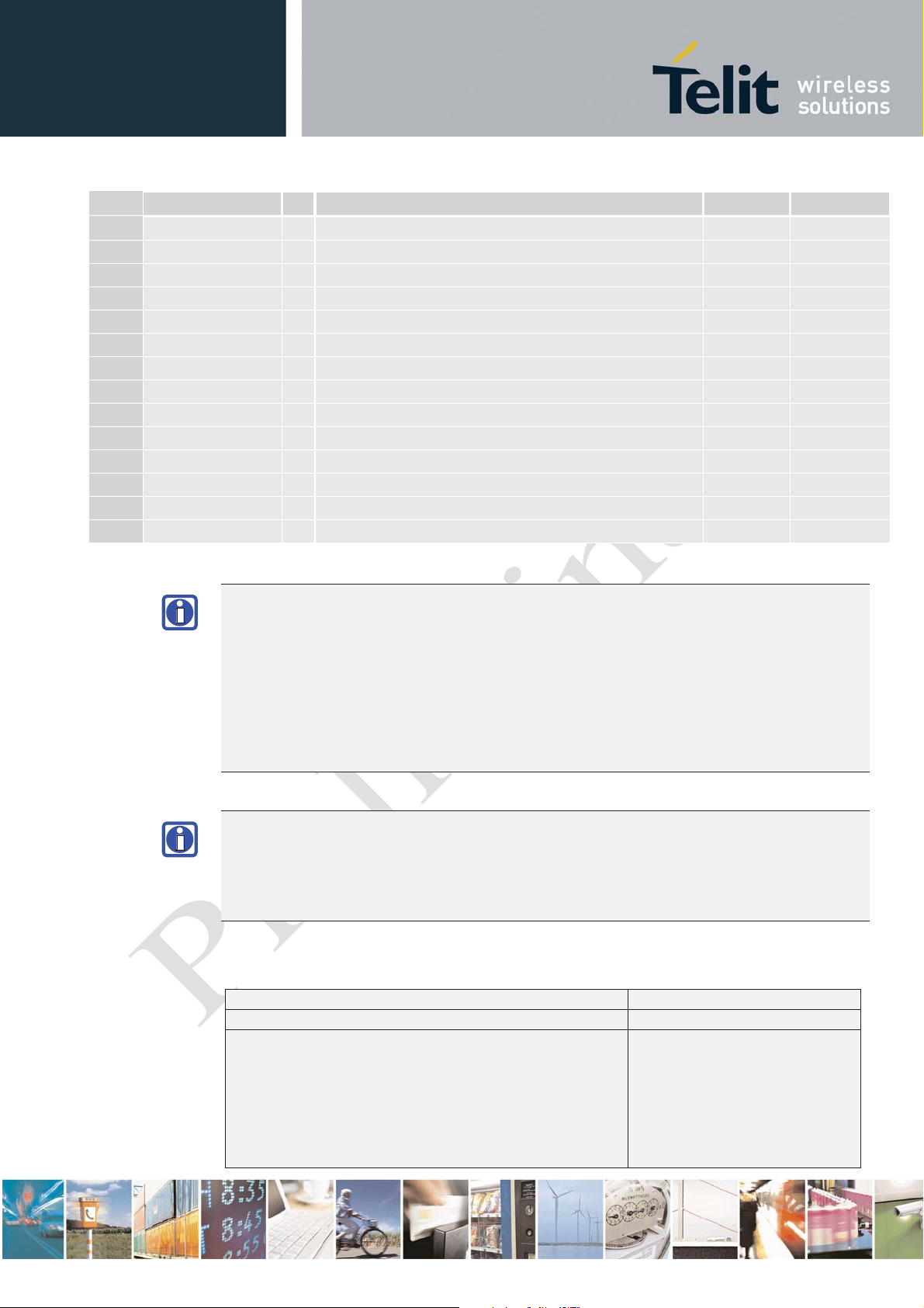
PAD Signal I/O Function Type COMMENT
AP3
AP5
AP7
AP9
AP11
AP13
AP15
AR2
AR4
AR6
AR8
AR10
AR12
AR14
AR16
AS5
AS7
AS9
AS11
AS13
AS15
AT4
AT6
AT8
AT10
AT12
AT14
AT16
AU1
AU5
AU7
AU11
AU15
GND - Ground
GND - Ground
GND - Ground
GND - Ground
GND - Ground
GND - Ground
GND - Ground
GND - Ground
GND - Ground
GND - Ground
GND - Ground
GND - Ground
GND - Ground
GND - Ground
GND - Ground
GND - Ground
GND - Ground
GND - Ground
GND - Ground
GND - Ground
GND - Ground
GND - Ground
GND - Ground
GND - Ground
GND - Ground
GND - Ground
GND - Ground
GND - Ground
GND - Ground
GND - Ground
GND - Ground
GND - Ground
GND - Ground
Reserved
C12
A14
A16
M17
AN6
V2
C14
Reserved - Reserved
Reserved - Reserved
Reserved - Reserved
Reserved - Reserved
Reserved - Reserved
Reserved - Reserved
Reserved - Reserved
Reproduction forbidden without written authorization from Telit Communications S.p.A. - All Rights Reserved. Page 20 of 76

L
LE920 Hardware User Guide
1vv0301026 Rev.0 - draft4 – 2013-05-
PAD Signal I/O Function Type COMMENT
D13
C16
D17
E16
C18
D15
F15
E4
E8
F3
F5
G2
H1
H3
H17
J2
J18
K1
K3
K17
K19
L2
L18
M3
M19
N18
P19
S3
S17
U3
U17
W3
W17
Y3
Y17
AB3
AB17
AD3
AD17
AF3
AF17
Reserved - Reserved
Reserved - Reserved
Reserved - Reserved
Reserved - Reserved
Reserved - Reserved
Reserved - Reserved
Reserved - Reserved
Reserved - Reserved
Reserved - Reserved
Reserved - Reserved
Reserved - Reserved
Reserved - Reserved
Reserved - Reserved
Reserved - Reserved
Reserved - Reserved
Reserved - Reserved
Reserved - Reserved
Reserved - Reserved
Reserved - Reserved
Reserved - Reserved
Reserved - Reserved
Reserved - Reserved
Reserved - Reserved
Reserved - Reserved
Reserved - Reserved
Reserved - Reserved
Reserved - Reserved
Reserved - Reserved
Reserved - Reserved
Reserved - Reserved
Reserved - Reserved
Reserved - Reserved
Reserved - Reserved
Reserved - Reserved
Reserved - Reserved
Reserved - Reserved
Reserved - Reserved
Reserved - Reserved
Reserved - Reserved
Reserved - Reserved
Reseved - Reserved
Reproduction forbidden without written authorization from Telit Communications S.p.A. - All Rights Reserved. Page 21 of 76
L
LE920 Hardware User Guide
1vv0301026 Rev.0 - draft4 – 2013-05-
PAD Signal I/O Function Type COMMENT
AH3
AH17
AK3
AL2
AM1
AM3
AN2
AN4
AN8
AN14
AS3
AT2
B19
AU13
Reserved - Reserved
Reserved - Reserved
Reserved - Reserved
Reserved - Reserved
Reserved - Reserved
Reserved - Reserved
Reserved - Reserved
Reserved - Reserved
Reserved - Reserved
Reserved - Reserved
Reserved - Reserved
Reserved - Reserved
Reserved - Reserved
Reserved - Reserved
NOTE:
When the UART signals are used as the communication port between the Host to the Modem:
- DTR pin must be connected in order to enter LE920’s power saving mode.
- RI pin must be connected in order to wake up the host when a call is coming in sleep
mode of host.
- RTS must be connected to the GND (on the module side) if flow control is not used
In case UART port isn’t used, all UART signals may be left disconnected
NOTE:
RESERVED pins must not be connected
NOTE:
If not used, almost all pins must be left disconnected. The only exceptions are the following:
PAD Signal
AP17,AP19,AR18,AS17,AS19,AT18,AU17,AU19 VBATT & VBATT_PA
A6,A12,B13,B15,B17,C4,C6,D3,D7,E18,F1,G18,H19,
M1,N2,P1,P3,R2,T2,T18,U1,V18,W1,X2,X18,Y1,Y19,
AA2,AB1,AC2,AE2,AF1,AG2,AH1,AJ2,AK1,AK17,
AL18,AM17,AM19,AN16,AN18,AP3,AP5,AP7,AP9,
GND
AP11,AP13,AP15,AR2,AR4AR6,AR8,AR10,AR12,
AR14,AR16,AS5,AS7,AS9,AS11,AS13,AS15,AT4,
AT6,AT8,AT10,AT12,AT14,AT16,AU1,AU5,AU7,
Reproduction forbidden without written authorization from Telit Communications S.p.A. - All Rights Reserved. Page 22 of 76

L
LE920 Hardware User Guide
1vv0301026 Rev.0 - draft4 – 2013-05-
AU11,AU15
AS1 ON/OFF*
Reproduction forbidden without written authorization from Telit Communications S.p.A. - All Rights Reserved. Page 23 of 76
 Loading...