

Telit Communications S p A LE910NA, LE910NV, LE910SV User Manual

PRODUCT
LE910-EUG
LE910-NAG
LE910-NVG
LE910-SVG
LE910-SKG
LE910 Hardware User Guide
1vv0301089 Rev.3 – 09-06-2014
Applicability Table
Reproduction forbidden without Telit Communications S.p.A. written authorization - All Rights Reserved page 2 of 79

LE910 Hardware User Guide
1vv0301089 Rev.3 – 09-06-2014
SPECIFICATIONS SUBJECT TO CHANGE WITHOUT NOTICE
Notice
While reasonable efforts have been made to assure the accuracy of this document, Telit assumes
no liability resulting from any inaccuracies or omissions in this document, or from use of the
information obtained herein. The information in this document has been carefully checked and is
believed to be entirely reliable. However, no responsibility is assumed for inaccuracies or
omissions. Telit reserves the right to make changes to any products described herein and
reserves the right to revise this document and to make changes from time to time in content
hereof with no obligation to notify any person of revisions or changes. Telit does not assume
any liability arising out of the application or use of any product, software, or circuit described
herein; neither does it convey license under its patent rights or the rights of others.
It is possible that this publication may contain references to, or information about Telit products
(machines and programs), programming, or services that are not announced in your country.
Such references or information must not be construed to mean that Telit intends to announce
such Telit products, programming, or services in your country.
Copyrights
This instruction manual and the Telit products described in this instruction manual may be,
include or describe copyrighted Telit material, such as computer programs stored in
semiconductor memories or other media. Laws in the Italy and other countries preserve for Telit
and its licensors certain exclusive rights for copyrighted material, including the exclusive right
to copy, reproduce in any form, distribute and make derivative works of the copyrighted
material. Accordingly, any copyrighted material of Telit and its licensors contained herein or in
the Telit products described in this instruction manual may not be copied, reproduced,
distributed, merged or modified in any manner without the express written permission of Telit.
Furthermore, the purchase of Telit products shall not be deemed to grant either directly or by
implication, estoppel, or otherwise, any license under the copyrights, patents or patent
applications of Telit, as arises by operation of law in the sale of a product.
Computer Software Copyrights
The Telit and 3rd Party supplied Software (SW) products described in this instruction manual
may include copyrighted Telit and other 3rd Party supplied computer programs stored in
semiconductor memories or other media. Laws in the Italy and other countries preserve for Telit
and other 3rd Party supplied SW certain exclusive rights for copyrighted computer programs,
including the exclusive right to copy or reproduce in any form the copyrighted computer
program. Accordingly, any copyrighted Telit or other 3rd Party supplied SW computer programs
contained in the Telit products described in this instruction manual may not be copied (reverse
engineered) or reproduced in any manner without the express written permission of Telit or the
3rd Party SW supplier. Furthermore, the purchase of Telit products shall not be deemed to grant
either directly or by implication, estoppel, or otherwise, any license under the copyrights,
patents or patent applications of Telit or other 3rd Party supplied SW, except for the normal
non-exclusive, royalty free license to use that arises by operation of law in the sale of a product.
Reproduction forbidden without Telit Communications S.p.A. written authorization - All Rights Reserved page 3 of 79

LE910 Hardware User Guide
1vv0301089 Rev.3 – 09-06-2014
Usage and Disclosure Restrictions
License Agreements
The software described in this document is the property of Telit and its licensors. It is furnished
by express license agreement only and may be used only in accordance with the terms of such
an agreement.
Copyrighted Materials
Software and documentation are copyrighted materials. Making unauthorized copies is
prohibited by law. No part of the software or documentation may be reproduced, transmitted,
transcribed, stored in a retrieval system, or translated into any language or computer language,
in any form or by any means, without prior written permission of Telit
High Risk Materials
Components, units, or third-party products used in the product described herein are NOT faulttolerant and are NOT designed, manufactured, or intended for use as on-line control equipment
in the following hazardous environments requiring fail-safe controls: the operation of Nuclear
Facilities, Aircraft Navigation or Aircraft Communication Systems, Air Traffic Control, Life
Support, or Weapons Systems (High Risk Activities"). Telit and its supplier(s) specifically
disclaim any expressed or implied warranty of fitness for such High Risk Activities.
Trademarks
TELIT and the Stylized T Logo are registered in Trademark Office. All other product or service
names are the property of their respective owners.
Copyright © Telit Communications S.p.A. 2014
Reproduction forbidden without Telit Communications S.p.A. written authorization - All Rights Reserved page 4 of 79
LE910 Hardware User Guide
1vv0301089 Rev.3 – 09-06-2014
1 INTRODUCTION ......................................................................................................................................................... 7
1.1 SCOPE ................................................................................................................................................................................ 7
1.2 AUDIENCE ........................................................................................................................................................................... 7
1.3 CONTACT INFORMATION, SUPPORT .......................................................................................................................................... 7
1.4 DOCUMENT ORGANIZATION ................................................................................................................................................... 8
1.5 TEXT CONVENTIONS .............................................................................................................................................................. 9
1.6 RELATED DOCUMENTS ........................................................................................................................................................... 9
1.7 DOCUMENT HISTORY .......................................................................................................................................................... 10
2 OVERVIEW .............................................................................................................................................................. 11
3 LE910 MODULE CONNECTIONS................................................................................................................................ 12
3.1 PIN-OUT ......................................................................................................................................................................... 12
3.1.1 LGA Pads Layout ..................................................................................................................................................... 17
4 HARDWARE COMMANDS ........................................................................................................................................ 18
4.1 TURNING ON THE LE910 .................................................................................................................................................... 18
4.2 INITIALIZATION AND ACTIVATION STATE................................................................................................................................... 20
4.3 TURNING OFF THE LE910 ................................................................................................................................................... 21
4.3.1 Shutdown by Software Command .......................................................................................................................... 21
4.3.2 Hardware Shutdown .............................................................................................................................................. 22
4.4 LE910 UNCONDITIONAL SHUTDOWN ..................................................................................................................................... 23
4.5 SUMMARY OF TURNING ON AND OFF THE MODULE ................................................................................................................. 26
5 POWER SUPPLY ....................................................................................................................................................... 27
5.1 POWER SUPPLY REQUIREMENTS ............................................................................................................................................ 27
5.2 POWER CONSUMPTION ....................................................................................................................................................... 28
5.3 GENERAL DESIGN RULES ...................................................................................................................................................... 29
5.3.1 Electrical Design Guidelines ................................................................................................................................... 29
5.3.2 Thermal Design Guidelines ..................................................................................................................................... 33
5.3.3 Power Supply PCB layout Guidelines ...................................................................................................................... 34
6 GSM/WCDMA/LTE RADIO SECTION......................................................................................................................... 36
6.1 LE910 PRODUCT VARIANTS ................................................................................................................................................. 36
6.2 TX OUTPUT POWER ............................................................................................................................................................ 36
6.3 GSM/WCDMA/LTE ANTENNA REQUIREMENTS .................................................................................................................... 37
6.4 GSM/WCDMA/LTE - PCB LINE GUIDELINES ......................................................................................................................... 40
6.5 GSM/WCDMA/LTE ANTENNA - INSTALLATION GUIDELINES .................................................................................................... 41
6.6 ANTENNA DIVERSITY REQUIREMENTS ..................................................................................................................................... 41
7 GNSS RECEIVER ....................................................................................................................................................... 43
7.1 GNSS SIGNALS PINOUT ....................................................................................................................................................... 43
7.2 GPS/GLONASS ANTENNA REQUIREMENTS ............................................................................................................................ 43
7.2.1 GNSS Antenna - PCB Line Guidelines ...................................................................................................................... 44
7.2.2 RF Trace Losses....................................................................................................................................................... 44
7.2.3 GNSS Antenna - Installation ................................................................................................................................... 45
8 LOGIC LEVEL SPECIFICATIONS .................................................................................................................................. 46
Reproduction forbidden without Telit Communications S.p.A. written authorization - All Rights Reserved page 5 of 79

LE910 Hardware User Guide
1vv0301089 Rev.3 – 09-06-2014
9 UNCONDITIONAL SHUTDOWN ................................................................................................................................ 47
10 USB PORT ................................................................................................................................................................ 48
10.1 USB 2.0 HS DESCRIPTION ................................................................................................................................................. 48
11 SERIAL PORTS .......................................................................................................................................................... 49
11.1 MODEM SERIAL PORT 1 ............................................................................................................................................... 50
11.2 MODEM SERIAL PORT 2 (USIF1) ................................................................................................................................... 51
11.3 RS232 LEVEL TRANSLATION ................................................................................................................................................ 52
12 AUDIO SECTION OVERVIEW .................................................................................................................................... 54
12.1 ELECTRICAL CHARACTERISTICS ............................................................................................................................................. 54
13 GENERAL PURPOSE I/O ........................................................................................................................................... 55
13.1 GPIO LOGIC LEVELS .......................................................................................................................................................... 56
13.2 USING A GPIO PAD AS INPUT ........................................................................................................................................... 56
13.3 USING A GPIO PAD AS OUTPUT ........................................................................................................................................ 56
13.4 INDICATION OF NETWORK SERVICE AVAILABILITY ..................................................................................................................... 57
13.5 RTC BYPASS OUT ............................................................................................................................................................. 58
13.6 VAUX POWER OUTPUT ..................................................................................................................................................... 58
13.7 ADC CONVERTER ............................................................................................................................................................. 59
13.7.1 Description ........................................................................................................................................................... 59
13.7.2 Using ADC Converter ............................................................................................................................................ 59
14 MOUNTING THE LE910 ON THE APPLICATION ......................................................................................................... 60
14.1 GENERAL ........................................................................................................................................................................ 60
14.2 MODULE FINISHING & DIMENSIONS ..................................................................................................................................... 60
14.3 RECOMMENDED FOOT PRINT FOR THE APPLICATION ................................................................................................................. 62
14.4 STENCIL .......................................................................................................................................................................... 63
14.5 PCB PAD DESIGN .............................................................................................................................................................. 63
14.6 PCB PAD DIMENSIONS ....................................................................................................................................................... 64
14.7 SOLDER PASTE .................................................................................................................................................................. 66
14.7.1 LE910 Solder reflow .............................................................................................................................................. 66
14.8 PACKING SYSTEM (TRAY) .................................................................................................................................................... 68
14.9 PACKING SYSTEM (REEL) .................................................................................................................................................... 70
14.9.1 Carrier Tape Detail ............................................................................................................................................... 70
14.9.2 Reel Detail ............................................................................................................................................................ 71
14.9.3 Packaging Detail .................................................................................................................................................. 72
14.10 MOISTURE SENSITIVITY .................................................................................................................................................... 72
15 SAFETY RECOMMANDATIONS ................................................................................................................................. 73
16 CONFORMITY ASSESSMENT ISSUES ......................................................................................................................... 74
16.1 1999/5/EC DIRECTIVE ..................................................................................................................................................... 74
16.2 FCC/IC REGULATORY NOTICES ............................................................................................................................................ 77
Reproduction forbidden without Telit Communications S.p.A. written authorization - All Rights Reserved page 6 of 79
LE910 Hardware User Guide
1vv0301089 Rev.3 – 09-06-2014
The aim of this document is the description of some hardware solutions useful for developing a
product with the Telit LE910 module.
This document is intended for Telit customers, who are integrators, about to implement their
applications using our LE910 modules.
For general contact, technical support, to report documentation errors and to order manuals,
contact Telit’s Technical Support Center (TTSC) at:
TS-EMEA@telit.com
TS-NORTHAMERICA@telit.com
TS-LATINAMERICA@telit.com
TS-APAC@telit.com
Alternatively, use:
http://www.telit.com/en/products/technical-support-center/contact.php
For detailed information about where you can buy the Telit modules or for recommendations on
accessories and components visit:
http://www.telit.com
To register for product news and announcements or for product questions contact Telit’s
Technical Support Center (TTSC).
Our aim is to make this guide as helpful as possible. Keep us informed of your comments and
suggestions for improvements.
Telit appreciates feedback from the users of our information.
Reproduction forbidden without Telit Communications S.p.A. written authorization - All Rights Reserved page 7 of 79
LE910 Hardware User Guide
1vv0301089 Rev.3 – 09-06-2014
This document contains the following chapters:
Chapter 1: “Introduction” provides a scope for this document, target audience, contact and
support information, and text conventions.
Chapter 2: “Overview” provides an overview of the document.
Chapter3: “LE910 Module Connections” deals with the pin out configuration and layout.
Chapter 4: “Hardware Commands” How to operate on the module via hardware.
Chapter 5: “Power supply” Power supply requirements and general design rules.
Chapter 6: “GSM/WCDMA Radio” The antenna connection and board layout design are the
most important parts in the full product design.
Chapter 7: “GNSS Receiver” This section describes the GNSS receiver.
Chapter 8: “Logic Level specifications” Specific values adopted in the implementation of logic
levels for this module.
Chapter 9: “USB Port” The USB port on the Telit LE910 is the core of the interface between the
module and OEM hardware
Chapter 10: “SPI port” Refers to the SPI port of the Telit LE910
Chapter 11: “Serial ports” Refers to the serial ports of the Telit LE910
Chapter 12: “Audio Section overview” Refers to the audio blocks of the Base Band Chip of the
LE910 Telit Modules.
Chapter 13: “General Purpose I/O” How the general purpose I/O pads can be configured.
Chapter 14: “Mounting the LE910 on the application board” Mechanical dimensions and
recommendations on how to mount the module on the user’s board.
Chapter 15: “Safety Recommendations” Information related to the Safety topics.
Chapter 16: “Conformity Assessment Issues” Information related to the Conformity
Assessments.
Reproduction forbidden without Telit Communications S.p.A. written authorization - All Rights Reserved page 8 of 79

LE910 Hardware User Guide
1vv0301089 Rev.3 – 09-06-2014
Danger – This information MUST be followed or catastrophic equipment failure or bodily
injury may occur.
Caution or Warning – Alerts the user to important points about integrating the module, if
these points are not followed, the module and end user equipment may fail or malfunction.
Tip or Information – Provides advice and suggestions that may be useful when integrating
the module.
All dates are in ISO 8601 format, i.e. YYYY-MM-DD.
LE910 Product description 80421ST10587a
SIM Holder Design Guides 80000NT10001a
AT Commands Reference Guide 80421ST10585A
Telit EVK2 User Guide 1vv0300704
Reproduction forbidden without Telit Communications S.p.A. written authorization - All Rights Reserved page 9 of 79
RReevviissiioonn
DDaattee
CChhaannggeess
ISSUE#0
2013-11-07
Preliminary Version
ISSUE#1
2013-12-20
Updated schematics & tray drawing;
ISSUE#2
2014-05-12
Added LE910-SVG and LE910-SKG; LE910-EUG now Dual Band 2G
(900/1800); added B5 WCDMA on LE910-EUG.
ISSUE#3
2014-06-19
Added Conformity assessment issues section for LE910-NVG, SVG and
NAG; updated chapter 10 (USB).
LE910 Hardware User Guide
1vv0301089 Rev.3 – 09-06-2014
Reproduction forbidden without Telit Communications S.p.A. written authorization - All Rights Reserved page 10 of 79
LE910
LE910 Hardware User Guide
1vv0301089 Rev.3 – 09-06-2014
The aim of this document is the description of some hardware solutions useful for developing a
product with the Telit LE910 module.
In this document all the basic functions of a mobile phone will be taken into account; for each
one of them a proper hardware solution will be suggested and eventually the wrong solutions
and common errors to be avoided will be evidenced. Obviously this document cannot embrace
the whole hardware solutions and products that may be designed. The wrong solutions to be
avoided shall be considered as mandatory, while the suggested hardware configurations shall not
be considered mandatory, instead the information given shall be used as a guide and a starting
point for properly developing your product with the Telit LE910 module. For further hardware
details that may not be explained in this document refer to the Telit LE910 Product Description
document where all the hardware information is reported.
NOTICE:
(EN) The integration of the GSM/GPRS/WCDMA/LTE LE910 cellular module within user application
shall be done according to the design rules described in this manual.
(IT) L’integrazione del modulo cellulare GSM/GPRS/WCDMA/LTE LE910 all’interno dell’applicazione
dell’utente dovrà rispettare le indicazioni progettuali descritte in questo manuale.
(DE) Die Integration des LE910 GSM/GPRS/WCDMA/LTE Mobilfunk-Moduls in ein Gerät muß gemäß
der in diesem Dokument beschriebenen Kunstruktionsregeln erfolgen.
(SL) Integracija GSM/GPRS/WCDMA/LTE LE910 modula v uporabniški aplikaciji bo morala upoštevati
projektna navodila, opisana v tem priročniku.
(SP) La utilización del modulo GSM/GPRS/WCDMA/LTE LE910 debe ser conforme a los usos para los
cuales ha sido deseñado descritos en este manual del usuario.
(FR) L’intégration du module cellulaire GSM/GPRS/WCDMA/LTE LE910 dans l’application de
l’utilisateur sera faite selon les règles de conception décrites dans ce manuel.
(HE)
The information presented in this document is believed to be accurate and reliable. However, no
responsibility is assumed by Telit Communications S.p.A. for its use, nor any infringement of patents or
other rights of third parties which may result from its use. No license is granted by implication or
otherwise under any patent rights of Telit Communications S.p.A. other than for circuitry embodied in
Telit products. This document is subject to change without notice.
Reproduction forbidden without Telit Communications S.p.A. written authorization - All Rights Reserved page 11 of 79
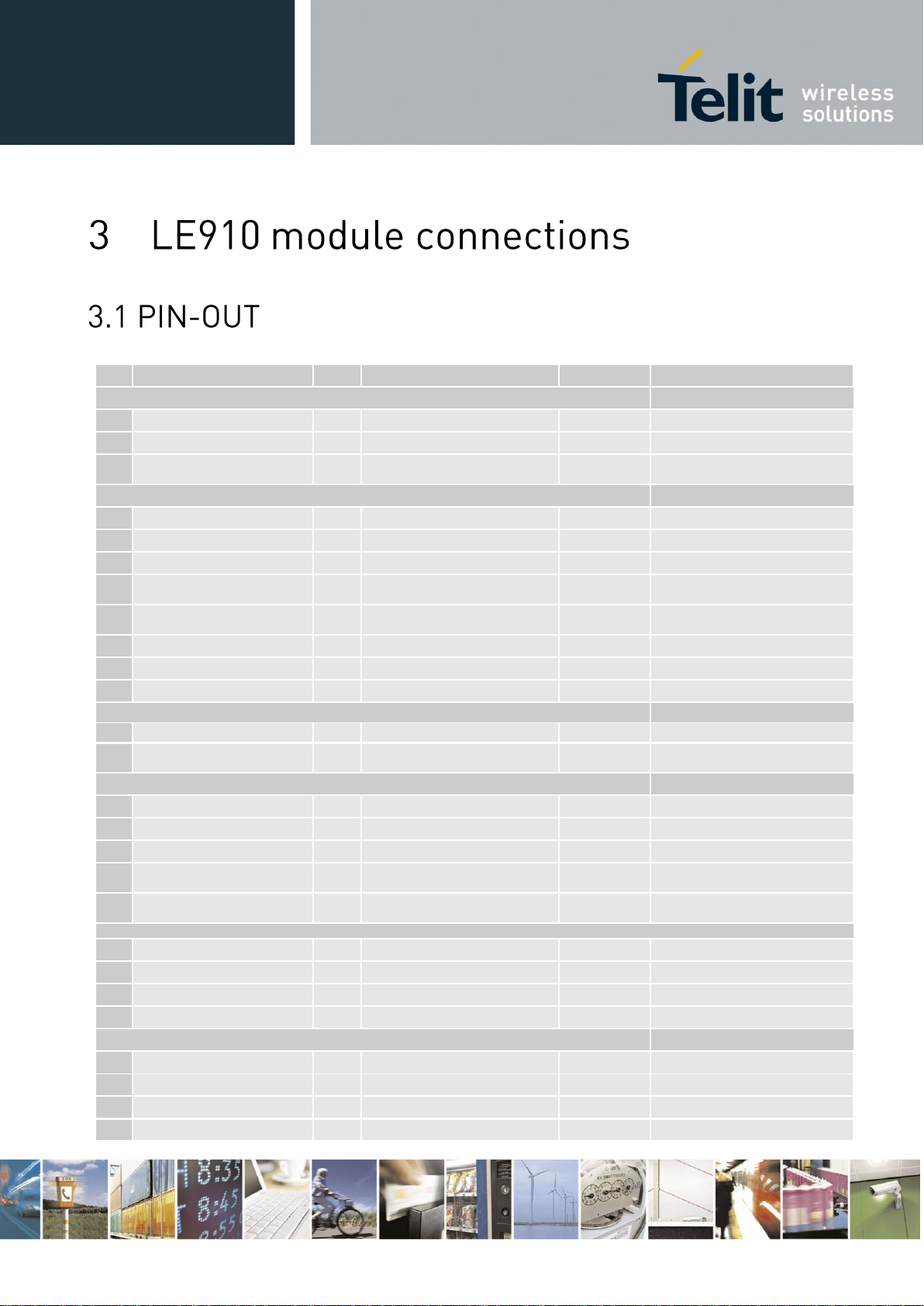
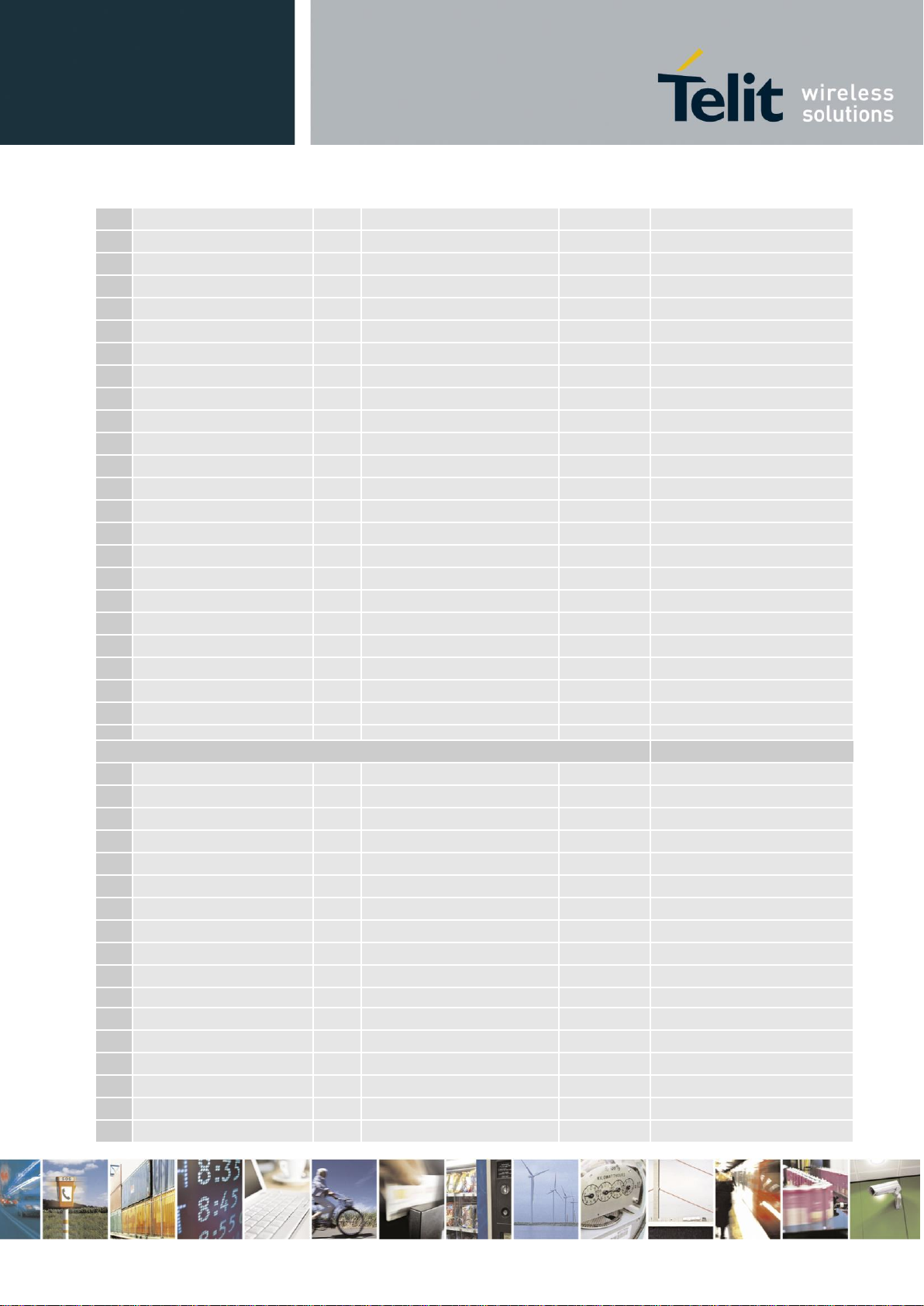
PAD
Signal
I/O
Function
Type
COMMENT
USB HS 2.0 COMMUNICATION PORT
B15
USB_D+
I/O
USB differential Data (+)
C15
USB_D-
I/O
USB differential Data (-)
A13
VUSB
I
Power sense for the internal USB
transceiver.
Asynchronous Serial Port (USIF0) – Prog. / Data + HW Flow Control
N15
C103/TXD
I
Serial data input from DTE
CMOS 1.8V
M15
C104/RXD
O
Serial data output to DTE
CMOS 1.8V
M14
C108/DTR
I
Input for (DTR) from DTE
CMOS 1.8V
L14
C105/RTS
I
Input for Request to send signal
(RTS) from DTE
CMOS 1.8V
P15
C106/CTS
O
Output for Clear to Send signal
(CTS) to DTE
CMOS 1.8V
N14
C109/DCD
O
Output for (DCD) to DTE
CMOS 1.8V
P14
C107/DSR
O
Output for (DSR) to DTE
CMOS 1.8V
R14
C125/RING
O
Output for Ring (RI) to DTE
CMOS 1.8V
Asynchronous Auxiliary Serial Port (USIF1)
D15
TX_AUX
O
Auxiliary UART (TX Data to DTE)
CMOS 1.8V
E15
RX_AUX
I
Auxiliary UART (RX Data from
DTE)
CMOS 1.8V
SIM card interface
A6
SIMCLK
O
External SIM signal – Clock
1.8 / 3V
A7
SIMRST
O
External SIM signal – Reset
1.8 / 3V
A5
SIMIO
I/O
External SIM signal – Data I/O
1.8 / 3V
A4
SIMIN
I
External SIM signal – Presence
(active low)
CMOS 1.8
A3
SIMVCC
-
External SIM signal – Power supply
for the SIM
1.8 / 3V
Digital Voice Interface (DVI)
B9
DVI_WA0
I/O
Digital Audio Interface (WA0)
1.8V
B6
DVI_RX
I
Digital Audio Interface (RX)
1.8V
B7
DVI_TX
I/O
Digital Audio Interface (TX)
1.8V
B8
DVI_CLK
I/O
Digital Audio Interface (CLK)
1.8V
DIGITAL IO
C8
GPIO_01
I/O
GPIO_01 /STAT LED
CMOS 1.8V
Alternate Function STAT LED
C9
GPIO_02
I/O
GPIO_02
CMOS 1.8V
C10
GPIO_03
I/O
GPIO_03
CMOS 1.8V
C11
GPIO_04
I/O
GPIO_04
CMOS 1.8V
LE910 Hardware User Guide
1vv0301089 Rev.3 – 09-06-2014
Reproduction forbidden without Telit Communications S.p.A. written authorization - All Rights Reserved page 12 of 79
B14
GPIO_05
I/O
GPIO_05
CMOS 1.8V
C12
GPIO_06
I/O
GPIO_06
CMOS 1.8V
C13
GPIO_07
I/O
GPIO_07
CMOS 1.8V
K15
GPIO_08
I/O
GPIO_08
CMOS 1.8V
L15
GPIO_09
I/O
GPIO_09
CMOS 1.8V
G15
GPIO_10
I/O
GPIO_10
CMOS 1.8V
ADC
B1
ADC_IN1
AI
Analog / Digital converter input
A/D
RF SECTION
K1
ANTENNA
I/O
GSM/EDGE/UMTS Antenna
(50 ohm)
RF
F1
ANT_DIV
I
Antenna Diversity Input
(50 ohm)
RF
GNSS SECTION (see NOTE1)
R9
ANT_GNSS
I
GNSS Antenna (50 ohm)
RF
R7
GNSS_LNA_EN
O
Output enable for External LNA
supply
CMOS 1.8V
Miscellaneous Functions
R13
HW_SHUTDOWN*
I
HW Unconditional Shutdown
1.8V
Active low
R12
ON_OFF*
I
Input command for power ON
1.8V
Active low
C14
VRTC
I
VRTC Backup capacitor
Power
backup for the embedded RTC supply
R11
VAUX/PWRMON
O
Supply Output for external
accessories / Power ON Monitor
1.8V
Power Supply
M1
VBATT
-
Main power supply (Baseband)
Power
M2
VBATT
-
Main power supply (Baseband)
Power
N1
VBATT_PA
-
Main power supply (Radio PA)
Power
N2
VBATT_PA
-
Main power supply (Radio PA)
Power
P1
VBATT_PA
-
Main power supply (Radio PA)
Power
P2
VBATT_PA
-
Main power supply (Radio PA)
Power
E1
GND - Ground
Power
G1
GND - Ground
Power
H1
GND - Ground
Power
J1
GND - Ground
Power
L1
GND - Ground
Power
A2
GND - Ground
Power
E2
GND - Ground
Power
F2
GND - Ground
Power
G2
GND - Ground
Power
H2
GND - Ground
Power
J2
GND - Ground
Power
K2
GND - Ground
Power
L2
GND - Ground
Power
R2
GND - Ground
Power
LE910 Hardware User Guide
1vv0301089 Rev.3 – 09-06-2014
Reproduction forbidden without Telit Communications S.p.A. written authorization - All Rights Reserved page 13 of 79
M3
GND - Ground
Power
N3
GND - Ground
Power
P3
GND - Ground
Power
R3
GND - Ground
Power
D4
GND - Ground
Power
M4
GND - Ground
Power
N4
GND - Ground
Power
P4
GND - Ground
Power
R4
GND - Ground
Power
N5
GND - Ground
Power
P5
GND - Ground
Power
R5
GND - Ground
Power
N6
GND - Ground
Power
P6
GND - Ground
Power
R6
GND - Ground
Power
P8
GND - Ground
Power
R8
GND - Ground
Power
P9
GND - Ground
Power
P10
GND - Ground
Power
R10
GND - Ground
Power
M12
GND - Ground
Power
B13
GND - Ground
Power
P13
GND - Ground
Power
E14
GND - Ground
Power
RESERVED
C1
RESERVED
-
RESERVED
D1
RESERVED
-
RESERVED
B2
RESERVED
-
RESERVED
C2
RESERVED
-
RESERVED
D2
RESERVED
-
RESERVED
B3
RESERVED
-
RESERVED
C3
RESERVED
-
RESERVED
D3
RESERVED
-
RESERVED
E3
RESERVED
-
RESERVED
F3
RESERVED
-
RESERVED
G3
RESERVED
-
RESERVED
H3
RESERVED
-
RESERVED
J3
RESERVED
-
RESERVED
K3
RESERVED
-
RESERVED
L3
RESERVED
-
RESERVED
B4
RESERVED
-
RESERVED
C4
RESERVED
-
RESERVED
LE910 Hardware User Guide
1vv0301089 Rev.3 – 09-06-2014
Reproduction forbidden without Telit Communications S.p.A. written authorization - All Rights Reserved page 14 of 79

B5
RESERVED
-
RESERVED
C5
RESERVED
-
RESERVED
C6
RESERVED
-
RESERVED
C7
RESERVED
-
RESERVED
N7
RESERVED
-
RESERVED
P7
RESERVED
-
RESERVED
N8
RESERVED
-
RESERVED
N9
RESERVED
-
RESERVED
A10
RESERVED
-
RESERVED
N10
RESERVED
-
RESERVED
N11
RESERVED
-
RESERVED
P11
RESERVED
-
RESERVED
B12
RESERVED
-
RESERVED
D12
RESERVED
-
RESERVED
N12
RESERVED
-
RESERVED
P12
RESERVED
-
RESERVED
F14
RESERVED
-
RESERVED
G14
RESERVED
-
RESERVED
H14
RESERVED
-
RESERVED
J14
RESERVED
-
RESERVED
K14
RESERVED
-
RESERVED
N13
RESERVED
-
RESERVED
L13
RESERVED
-
RESERVED
J13
RESERVED
-
RESERVED
M13
RESERVED
-
RESERVED
K13
RESERVED
-
RESERVED
H13
RESERVED
-
RESERVED
G13
RESERVED
-
RESERVED
F13
RESERVED
-
RESERVED
A11
RESERVED
-
RESERVED
A12
RESERVED
-
RESERVED
B11
RESERVED
-
RESERVED
B10
RESERVED
-
RESERVED
A9
RESERVED
-
RESERVED
A8
RESERVED
-
RESERVED
D14
RESERVED
-
RESERVED
A14
RESERVED
-
RESERVED
D13
RESERVED
-
RESERVED
E13
RESERVED
-
RESERVED
F15
RESERVED
-
RESERVED
H15
RESERVED
-
RESERVED
J15
RESERVED
-
RESERVED
LE910 Hardware User Guide
1vv0301089 Rev.3 – 09-06-2014
Reproduction forbidden without Telit Communications S.p.A. written authorization - All Rights Reserved page 15 of 79
PAD
Signal
Notes
M1,M2,N1,N2,P1,P2
VBATT & VBATT_PA
E1,G1,H1,J1,L1,A2,E2,F2,G2,H2,
J2,K2,L2,R2,M3,N3,P3,R3,D4,M4,
N4,P4,R4,N5,P5,R5,N6,P6,R6,P8,
R8,P9,P10,R10,M12,B13,P13,E14
GND
R12
ON/OFF*
R13
HW_SHUTDOWN*
B15
USB_D+
If not used should be connected to a
Test Point or an USB connector
C15
USB_D-
If not used should be connected to a
Test Point or an USB connector
A13
VUSB
If not used should be connected to a
Test Point or an USB connector
N15
C103/TXD
If not used should be connected to a
Test Point
M15
C104/RXD
If not used should be connected to a
Test Point
D15
TXD_AUX
If not used should be connected to a
Test Point
E15
RXD_AUX
If not used should be connected to a
Test Point
K1
MAIN ANTENNA
F1
ANT_DIV
R9
ANT_GNSS
If the GNSS is not used it could be
left unconnected
LE910 Hardware User Guide
1vv0301089 Rev.3 – 09-06-2014
WARNING:
Reserved pins must not be connected.
If not used, almost all pins should be left disconnected. The only exceptions are the following
pins:
Reproduction forbidden without Telit Communications S.p.A. written authorization - All Rights Reserved page 16 of 79
RTS pin should be connected to the GND (on the module side) if flow control is not used.
The above pins are also necessary to debug the application when the module is assembled on it so we
recommend connecting them also to dedicated test point.
A B C D E F
G H J K L M N P R
1 ADC_IN1
RES
RES
GND
ANT_DIV
GND
GND
GND
ANT
GND
VBATT
VBATT_
PA
VBATT_
PA
2
GND
RES
RES
RES
GND
GND
GND
GND
GND
GND
GND
VBATT
VBATT_
PA
VBATT_
PA
GND
3
SIMVC
C
RES
RES
RES
RES
RES
RES
RES
RES
RES
RES
GND
GND
GND
GND
4
SIMIN
RES
RES
GND GND
GND
GND
GND
5
SIMIO
RES
RES GND
GND
GND
6
SIMCLK
DVI_RX
RES GND
GND
GND
7
SIMRS
T
DVI_TX
RES RES
RES
GNSS_L
NA_EN
8
RES
DVI_CLK
GPIO_01 RES
GND
GND
9
RES
DVI_WA
0
GPIO_02 RES
GND
ANT_GN
SS
10
RES
RES
GPIO_03 RES
GND
GND
11
RES
RES
GPIO_04 RES
RES
VAUX/P
WRMON
12
RES
RES
GPIO_06
RES GND
RES
RES
ON_OFF
*
13
VUSB
GND
GPIO_07
VDD_IO
1
1V8_SEL
RES
RES
RES
RES
RES
RES
RES
RES
GND
HW_SH
UTDOW
N*
14
RES
GPIO_05
VRTC
RES
GND
RES
RES
RES
RES
RES
C105/RTS C108/DT
R
C109/DCD C107/DSR C125/RI
NG
15 USB_D+
USB_D-
TX AUX
RX AUX
RES
GPIO_10
RES
RES
GPIO_08
GPIO_09
C104/RX
D
C103/TXD C106/CT
S
LE910 Hardware User Guide
1vv0301089 Rev.3 – 09-06-2014
NOTE:
The pin defined as RES has to be considered RESERVED and not connected on any pin in the
application.
Reproduction forbidden without Telit Communications S.p.A. written authorization - All Rights Reserved page 17 of 79
LE910 Hardware User Guide
1vv0301089 Rev.3 – 09-06-2014
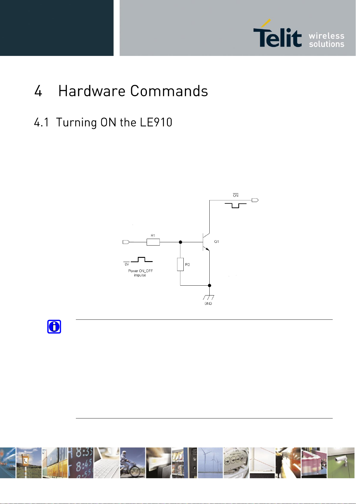
To turn on the LE910 the pad ON_OFF* must be tied low for at least 1 seconds and then
released.
The maximum current that can be drained from the ON_OFF* pad is 0,1 mA.
A simple circuit to do it is:
NOTE:
Don’t use any pull up resistor on the ON_OFF* line, it is internally pulled up. Using pull up
resistor may bring to latch up problems on the LE910 power regulator and improper power
on/off of the module. The line ON_OFF* must be connected only in open collector or open
drain configuration.
NOTE:
In this document all the lines that are inverted, hence have active low signals are labelled with a
name that ends with”#”,”*” or with a bar over the name.
TIP:
To check if the device has powered on, the hardware line PWRMON should be monitored.
Reproduction forbidden without Telit Communications S.p.A. written authorization - All Rights Reserved page 18 of 79
LE910 Hardware User Guide
1vv0301089 Rev.3 – 09-06-2014
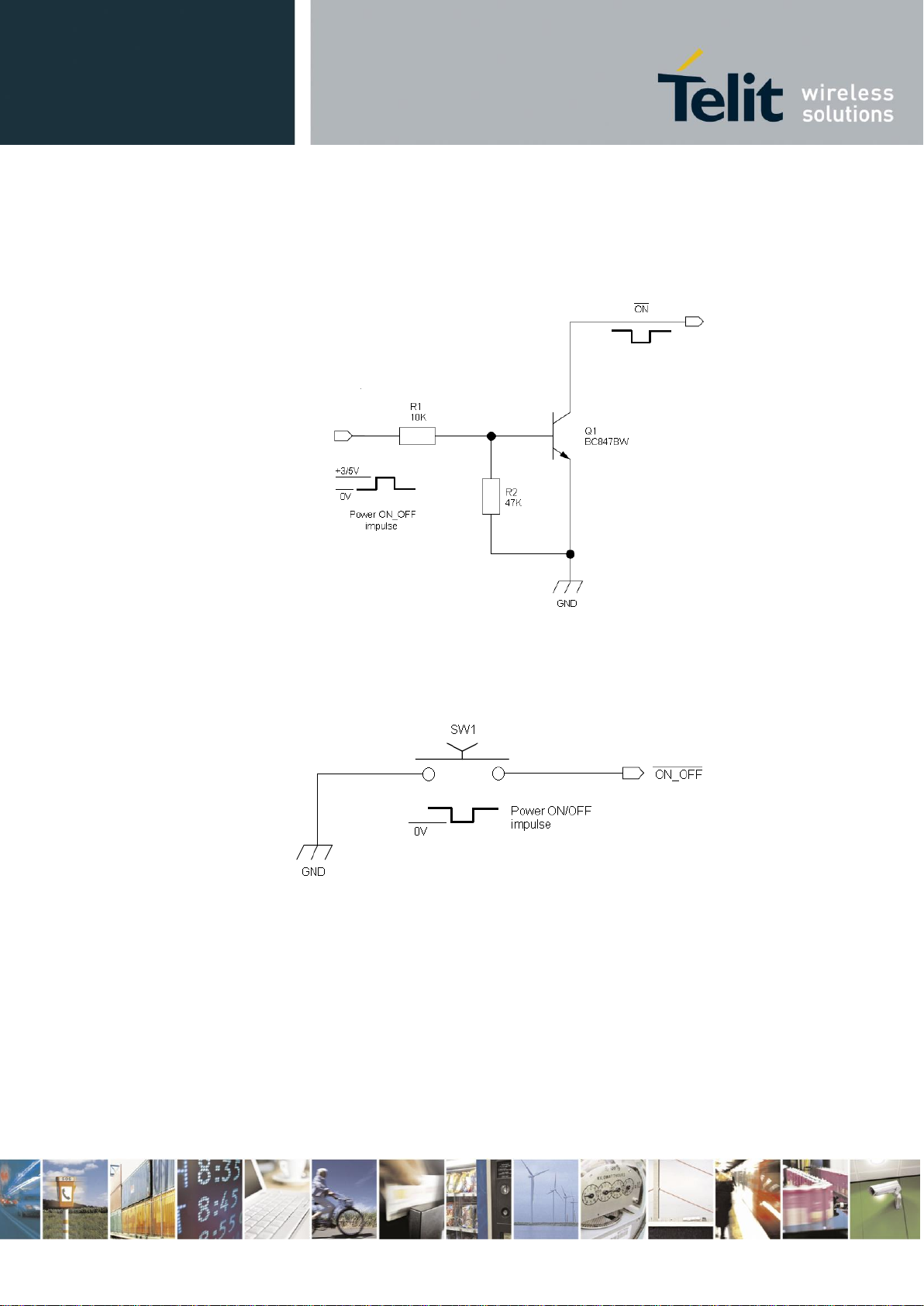
For example:
1- Let’s assume you need to drive the ON_OFF* pad with a totem pole output of a +3/5 V
microcontroller (uP_OUT1):
2- Let’s assume you need to drive the ON_OFF* pad directly with an ON/OFF button:
Reproduction forbidden without Telit Communications S.p.A. written authorization - All Rights Reserved page 19 of 79
LE910 Hardware User Guide
1vv0301089 Rev.3 – 09-06-2014
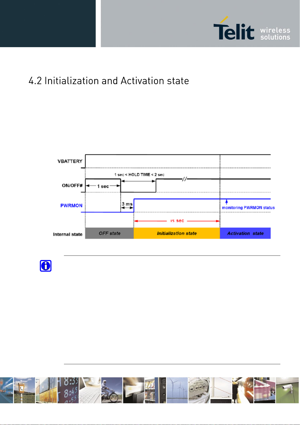
Upon turning on LE910 module, The LE910 is not activated yet because the boot sequence of
LE910 is still going on internally. It takes about 10 seconds to complete the initializing the
module internally.
For this reason, it would be useless to try to access LE910 during the Initialization state as
below.
To get the desirable stability, the LE910 needs at least 15 seconds after the PWRMON goes high
to become operational by reaching the activation state.
NOTE:
Don’t use any pull up resistor on the ON_OFF* line, it is internally pulled up. Using pull up
resistor may bring to latch up problems on the LE910 power regulator and improper power
on/off of the module. The line ON_OFF* must be connected only in open collector or open
drain configuration.
In this document all the lines that are inverted, hence have active low signals are labelled with a
name that ends with”#”,”*” or with a bar over the name.
During the Initialization state, any kind of AT-command is not available. DTE must be waiting
for the Activation state to communicate with LE910.
To check if the device has powered on, the hardware line PWRMON should be monitored.
Reproduction forbidden without Telit Communications S.p.A. written authorization - All Rights Reserved page 20 of 79
LE910 Hardware User Guide
1vv0301089 Rev.3 – 09-06-2014
Turning off of the device can be done in two ways:
via AT command (see LE910 Software User Guide, AT#SHDN)
by tying low pin ON_OFF*
Either ways, the device issues a detach request to network informing that the device will not
be reachable any more.
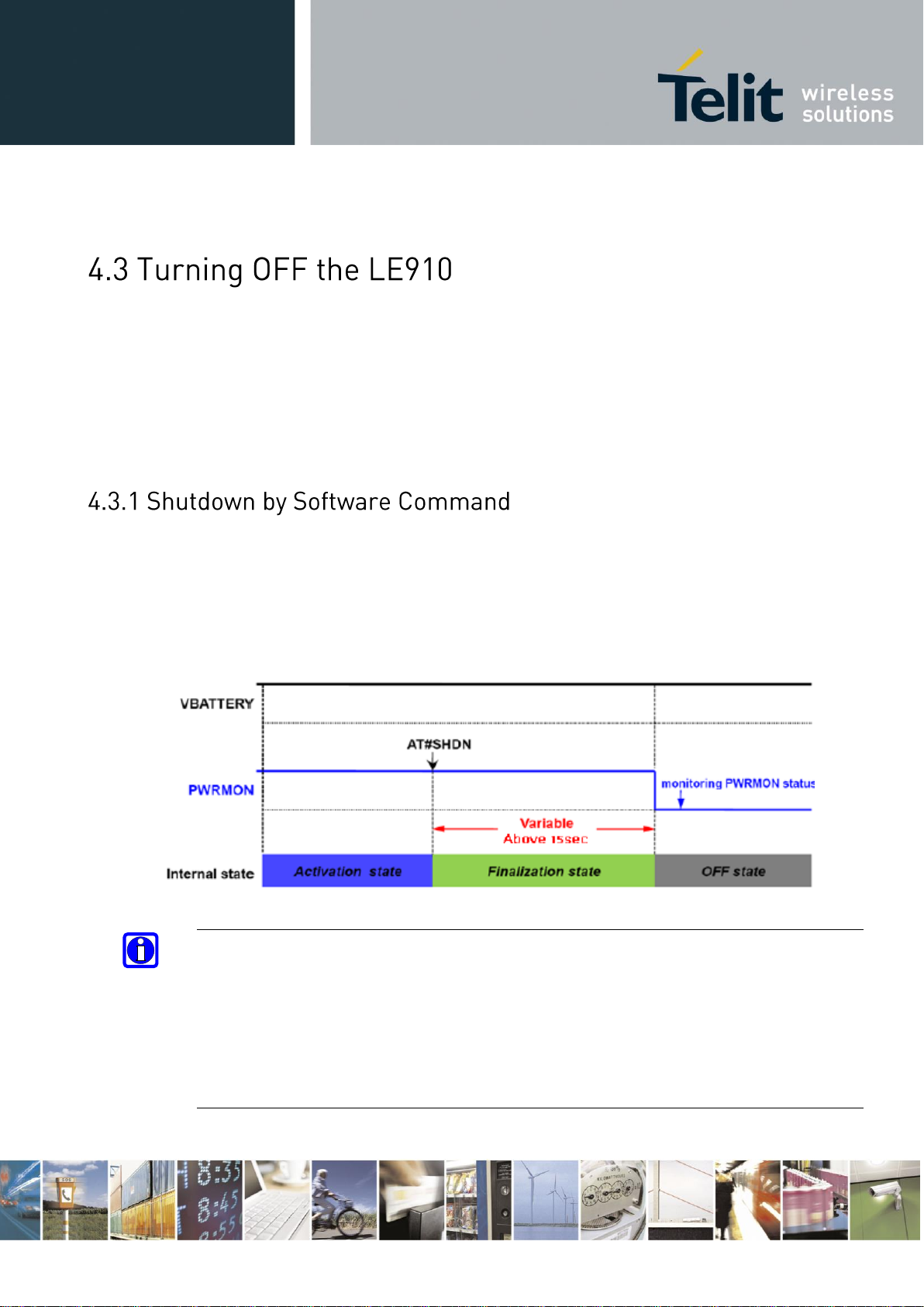
LE910 can be shut down using the AT#SHDN command.
When a shutdown command is sent, LE910 goes into the finalization state and finally will shut
down PWRMON at the end of this state.
The period of the finalization state can differ according to the situation in which the LE910 is so
it cannot be fixed definitely.
Normally it will be above 15 seconds later from sending a shutdown command and DTE should
monitor the status of PWRMON to see the actual power off.
TIP:
To check if the device has been powered off, the hardware line PWRMON must be monitored.
The device is powered off when PWRMON goes low.
NOTE:
In order to avoid a back powering effect it is recommended to avoid having any HIGH logic
level signal applied to the digital pins of the LE910 when the module is powered off or during
an ON/OFF transition.
Reproduction forbidden without Telit Communications S.p.A. written authorization - All Rights Reserved page 21 of 79
LE910 Hardware User Guide
1vv0301089 Rev.3 – 09-06-2014
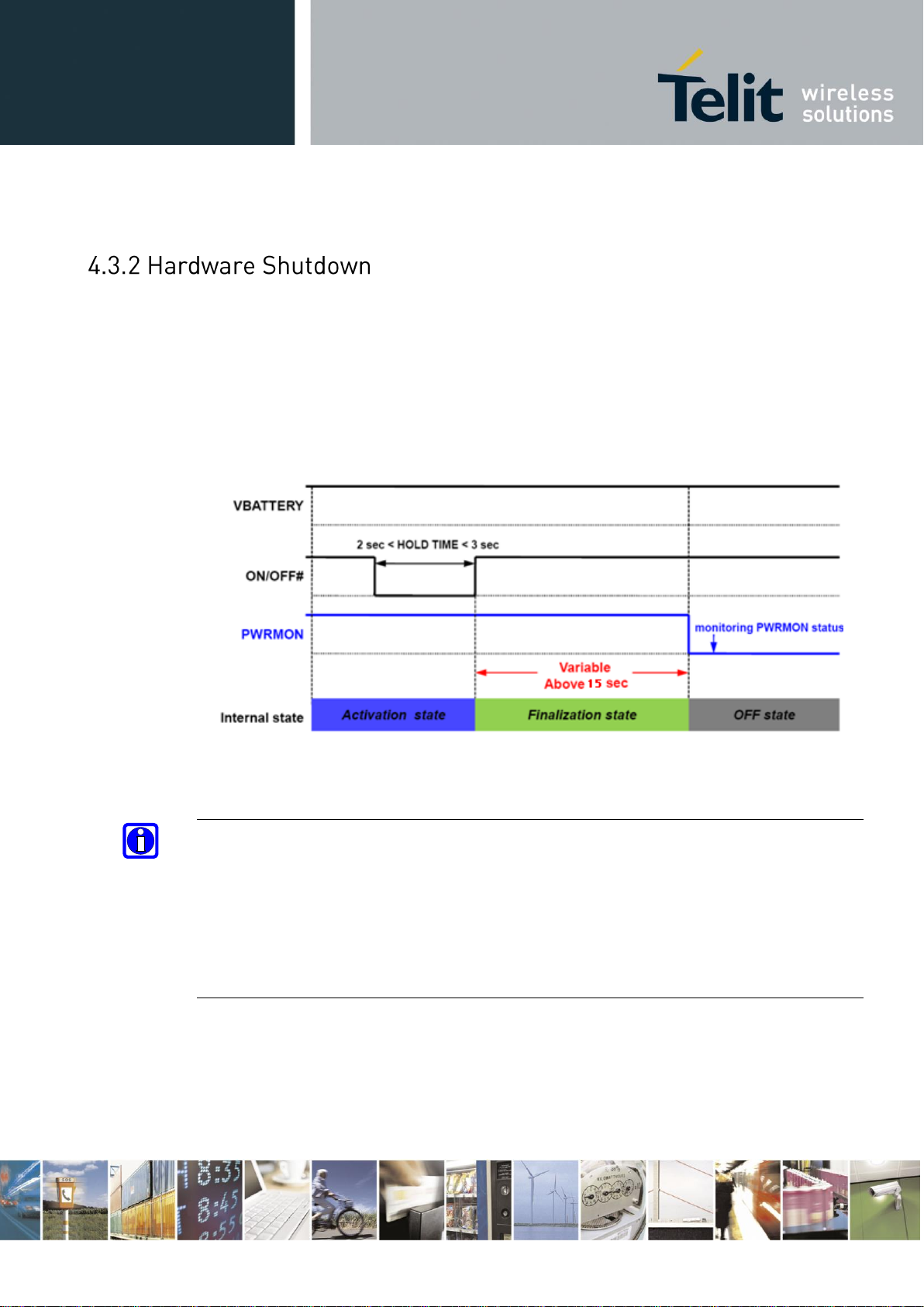
To turn OFF LE910 the pad ON/OFF# must be tied low for at least 2 seconds and then
released. Same circuitry and timing for the power on must be used.
When the hold time of ON/OFF# is above 2 seconds, LE910 goes into the finalization state
and finally will shut down PWRMON at the end of this state.
The period of the finalization state can differ according to the situation in which the LE910 is
so it cannot be fixed definitely.
Normally it will be above 15 seconds later from releasing ON/OFF# and DTE should monitor
the status of PWRMON to see the actual power off.
TIP:
To check if the device has been powered off, the hardware line PWRMON must be monitored.
The device is powered off when PWRMON goes low.
NOTE:
In order to avoid a back powering effect it is recommended to avoid having any HIGH logic
level signal applied to the digital pins of the LE910 when the module is powered off or during
an ON/OFF transition.
Reproduction forbidden without Telit Communications S.p.A. written authorization - All Rights Reserved page 22 of 79
LE910 Hardware User Guide
1vv0301089 Rev.3 – 09-06-2014
The Unconditional Shutdown of the module could be activated using the
HW_SHUTDOWN* line (pad R13).
WARNING:
The hardware unconditional Shutdown must not be used during normal operation of the device
since it does not detach the device from the network. It shall be kept as an emergency exit
procedure.
To unconditionally shutdown the LE910, the pad HW_SHUTDOWN* must be tied low for at
least 200 milliseconds and then released.
NOTE:
Do not use any pull up resistor on the HW_SHUTDOWN* line nor any totem pole digital
output. Using pull up resistor may bring to latch up problems on the LE910 power regulator and
improper functioning of the module. The line HW_SHUTDOWN* must be connected only in
open collector configuration.
The HW_SHUTDOWN* is generating an unconditional shutdown of the module without an
automatic restart.
The module will shutdown, but will NOT perform the detach from the cellular network.
To proper power on again the module please refer to the related paragraph (“Powering ON the
HE910”)
TIP:
The unconditional hardware shutdown must always be implemented on the boards and should be
used only as an emergency exit procedure.
Reproduction forbidden without Telit Communications S.p.A. written authorization - All Rights Reserved page 23 of 79
LE910 Hardware User Guide
1vv0301089 Rev.3 – 09-06-2014
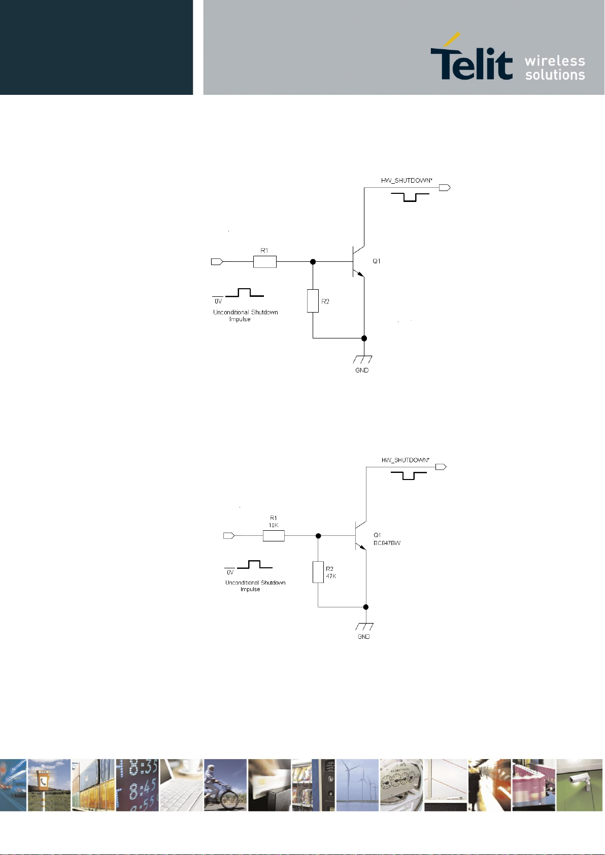
A typical circuit is the following:
For example:
1- Let us assume you need to drive the HW_SHUTDOWN* pad with a totem pole output of
a +3/5 V microcontroller (uP_OUT2):
Reproduction forbidden without Telit Communications S.p.A. written authorization - All Rights Reserved page 24 of 79
 Loading...