

Telit Communications S p A GM862 User Manual

T
elliitt
T
e
G
M
G
M
8
8
6
6
2--
2
Q
Q
U
U
Telit GM862-QUAD/-QUAD-PY
Hardware User Guide
1vv0300692, Rev. ISSUE#0, - 04/10/2005
A
D
A
D
G
M
G
M
H
arr
H
a
8
8
d
d
6
6
w
w
2--
2
arr
a
Q
Q
e
e
U
U
A
A
U
U
D--
D
s
err
s
e
P
P
Y
Y
G
G
uii
u
d
d
e
e
Telit Communications S.p.A. 2005
Reproduction forbidden without DAI Telecom written authorization – All Right reserved – Right of modification reserved page 1 of 69

Telit GM862-QUAD/-QUAD-PY
Hardware User Guide
1vv0300692, Rev. ISSUE#0, - 04/10/2005
Contents
1 OVERVIEW 4
2 HARDWARE COMMANDS 5
2.1 Turning ON the GM862-QUAD 5
2.2 Turning OFF the GM862-QUAD 7
2.2.1.1 Hardware shutdown 7
2.2.1.2 Hardware Unconditional Reset 7
3 POWER SUPPLY 9
3.1 Power Supply Requirements 9
3.2 General Design Rules 9
3.2.1 Electrical design Guidelines 10
3.2.1.1 + 5V input Source Power Supply Design Guidelines 10
3.2.1.2 + 12V input Source Power Supply Design Guidelines 11
3.2.1.3 Battery Source Power Supply Design Guidelines 12
3.2.1.4 Battery Charge control Circuitry Design Guidelines 12
3.2.2 Thermal Design Guidelines 14
3.2.3 Power Supply PCB layout Guidelines 15
4 SERIAL PORT 17
4.1 RS232 level translation 19
4.2 5V UART level translation 21
5 MICROPHONE 23
5.1 Microphone line Characteristic and requirements 23
5.2 General Design Rules 26
5.3 Microphone Biasing 26
5.3.1 Balanced Microphone biasing 27
5.3.2 Unbalanced Microphone biasing 28
5.4 Microphone buffering 29
5.4.1 Buffered Balanced Mic. 29
5.4.2 Buffered Unbalanced (Single Ended) Mic. 31
Reproduction forbidden without DAI Telecom written authorization – All Right reserved – Right of modification reserved page 2 of 69

Telit GM862-QUAD/-QUAD-PY
Hardware User Guide
1vv0300692, Rev. ISSUE#0, - 04/10/2005
6 SPEAKER 34
6.1 Speaker lines characteristics and requirements 34
6.2 General Design rules 36
6.2.1 Noise Filtering 36
6.3 Handset earphone design 36
6.4 Hands Free earphone (low power) design 38
6.5 Car Kit speakerphone design 38
7 GENERAL PURPOSE I/O 40
7.1 Using a GPIO pin as INPUT 40
7.2 Using a GPIO pin as OUTPUT 40
7.3 Using the Alarm Output GPIO6 41
7.4 Using the Buzzer Output GPIO7 41
8 CAMERA 42
8.1 Agilent Camera 42
8.1.1 Camera interface connectors 42
8.1.2 EVB for camera support 44
8.2 Camera Transchip 45
8.2.1 Camera interface connectors 45
8.2.2 EVB for Agilent and Transchip camera support 47
8.2.3 Block Diagram for supported cameras 48
8.2.4 Schematic Diagrams for supported cameras 49
8.2.5 Example usage script for camera 51
9 DOCUMENT CHANGE LOG 52
10 ANNEX A - EVK SCHEMATICS 53
11 ANNEX B - CAMERA EVB SCHEMATICS 65
Reproduction forbidden without DAI Telecom written authorization – All Right reserved – Right of modification reserved page 3 of 69

Telit GM862-QUAD/-QUAD-PY
Hardware User Guide
1vv0300692, Rev. ISSUE#0, - 04/10/2005
1 Overview
The aim of this document is the description of some hardware solutions useful for developing a
product with the Telit GM862-QUAD/-QUAD-PY modules.
In this document all the basic functions of a mobile phone will be taken into account; for each one
of them a proper hardware solution will be suggested and eventually the wrong solutions and
common errors to be avoided will be evidenced. Obviously this document can not embrace the
whole hardware solutions and products that may be designed. The wrong solutions to be avoided
shall be considered as mandatory, while the suggested hardware configurations shall not be
considered mandatory, instead the information given shall be used as a guide and a starting point for
properly developing your product with the Telit GM862-QUAD/-QUAD-PY modules. For further
hardware details that may not be explained in this document refer to the GM862-QUAD/-QUADPY Product Description document where all the hardware information is reported.
NOTE: In this document all the hardware solution are referenced to the GM862-QUAD.
As a general rule, since all the product line GM862-QUAD, GM862-QUAD-PY is pin to pin
hardware compatible, all these solutions apply also to the GM862-QUAD-PY.
NOTE
The information presented in this document is believed to be accurate and reliable. However, no responsibility is
assumed by DAI Telecom for its use, nor any infringement of patents or other rights of third parties which may result
from its use. No license is granted by implication or otherwise under any patent rights of DAI Telecom other than for
circuitry embodied in Telit products. This document is subject to change without notice
.
Reproduction forbidden without DAI Telecom written authorization – All Right reserved – Right of modification reserved page 4 of 69
Telit GM862-QUAD/-QUAD-PY
Hardware User Guide
1vv0300692, Rev. ISSUE#0, - 04/10/2005
2 Hardware Commands
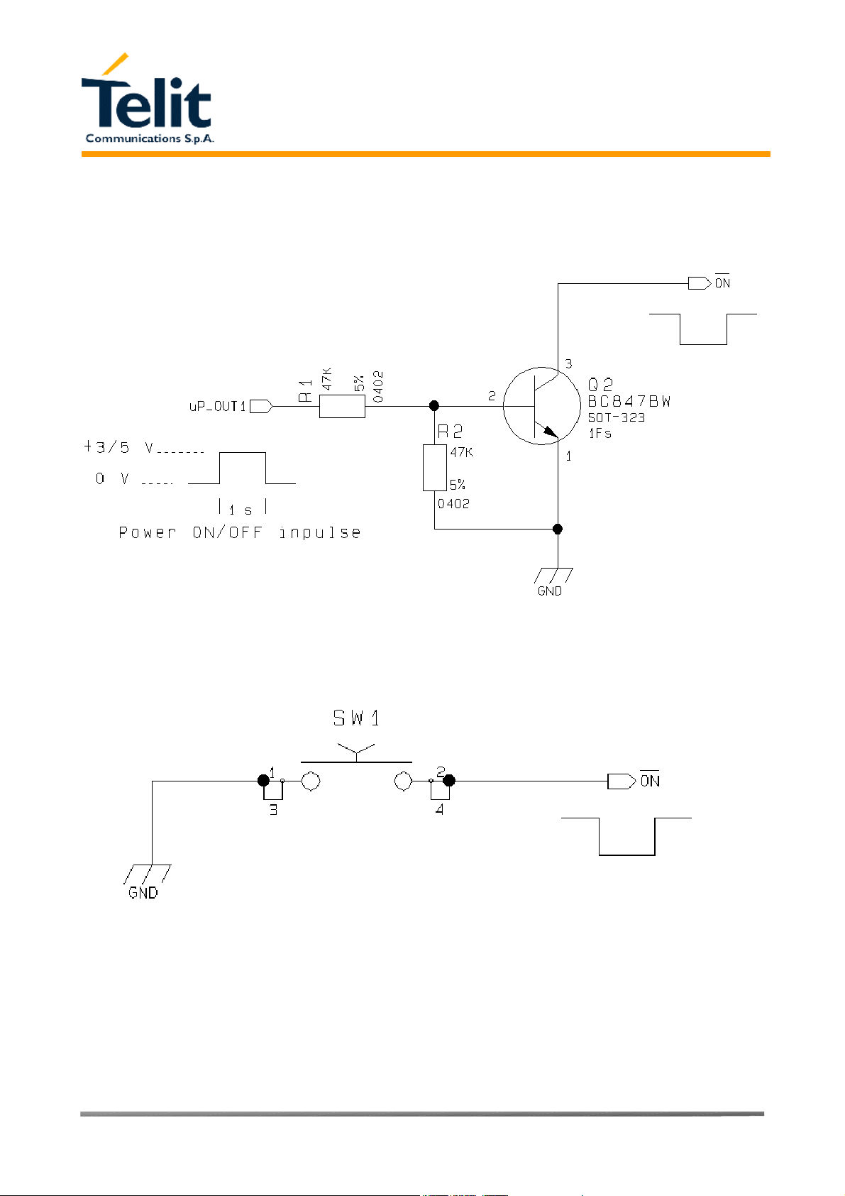
2.1 Turning ON the GM862-QUAD
To turn on the GM862-QUAD the pin ON# must be tied low for at least 1 second and then released.
The maximum current that can be drained from the ON# pin is 0,1 mA.
A simple circuit to do it is:
ON#
R1
Q1
Power ON impulse
R2
GND
NOTE: don't use any pull up resistor on the ON# line, it is internally pulled up. Using pull up resistor
may bring to latch up problems on the GM862-QUAD power regulator and improper power on/off of the
module. The line ON# must be connected only in open collector configuration.
NOTE: In this document all the lines that are inverted, hence have active low signals are labeled with a
name that ends with a "#" or with a bar over the name.
TIP: To check if power has raised it is possible to monitor the START line, when this line goes high the
module is powered on, but before it remains on the device needs other 900 ms for software startup.
Hence check the PWRCTL line and 900 ms after its transition to high it is possible to release the ON#
pin.
Reproduction forbidden without DAI Telecom written authorization – All Right reserved – Right of modification reserved page 5 of 69
Telit GM862-QUAD/-QUAD-PY
Hardware User Guide
1vv0300692, Rev. ISSUE#0, - 04/10/2005
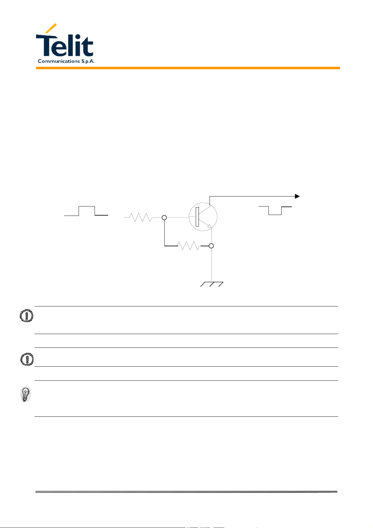
For example:
1- Let's assume you need to drive the ON# pin with a totem pole output of a +3/5 V microcontroller
(uP_OUT1):
2- Let's assume you need to drive the ON# pin directly with an ON/OFF button:
Reproduction forbidden without DAI Telecom written authorization – All Right reserved – Right of modification reserved page 6 of 69

Telit GM862-QUAD/-QUAD-PY
Hardware User Guide
1vv0300692, Rev. ISSUE#0, - 04/10/2005
2.2 Turning OFF the GM862-QUAD
The turning off of the device can be done in three ways:
• by software command (see GM862-QUAD Software User Guide)
• by hardware shutdown
• by hardware unconditional shutdown
When the device is shut down by software command or by hardware shutdown, it issues to the
network a detach request that informs the network that the device will not be reachable any more.
The hardware unconditional shutdown does not issue this request and shuts down immediately the
device.
The hardware unconditional shutdown must not be used during normal operation of the device
since it does not detach the device from the network. It shall be kept as an emergency exit
procedure to be done in the rare case that the device gets stucked waiting for some network or SIM
responses.
If device does not respond to a command in the timeout window, retry issuing the command and if
still no response is received a hardware unconditional shutdown shall be issued and then a restart.
2.2.1.1 Hardware shutdown
To turn OFF the GM862-QUAD the pin ON# must be tied low for at least 1 second and then
released.
The same circuitry and timing for the power on shall be used.
The device shuts down after the release of the ON# pin.
TIP: To check if the device has powered off, the hardware line PWRCTL should be monitored. When
PWRCTL goes low, the device has powered off.
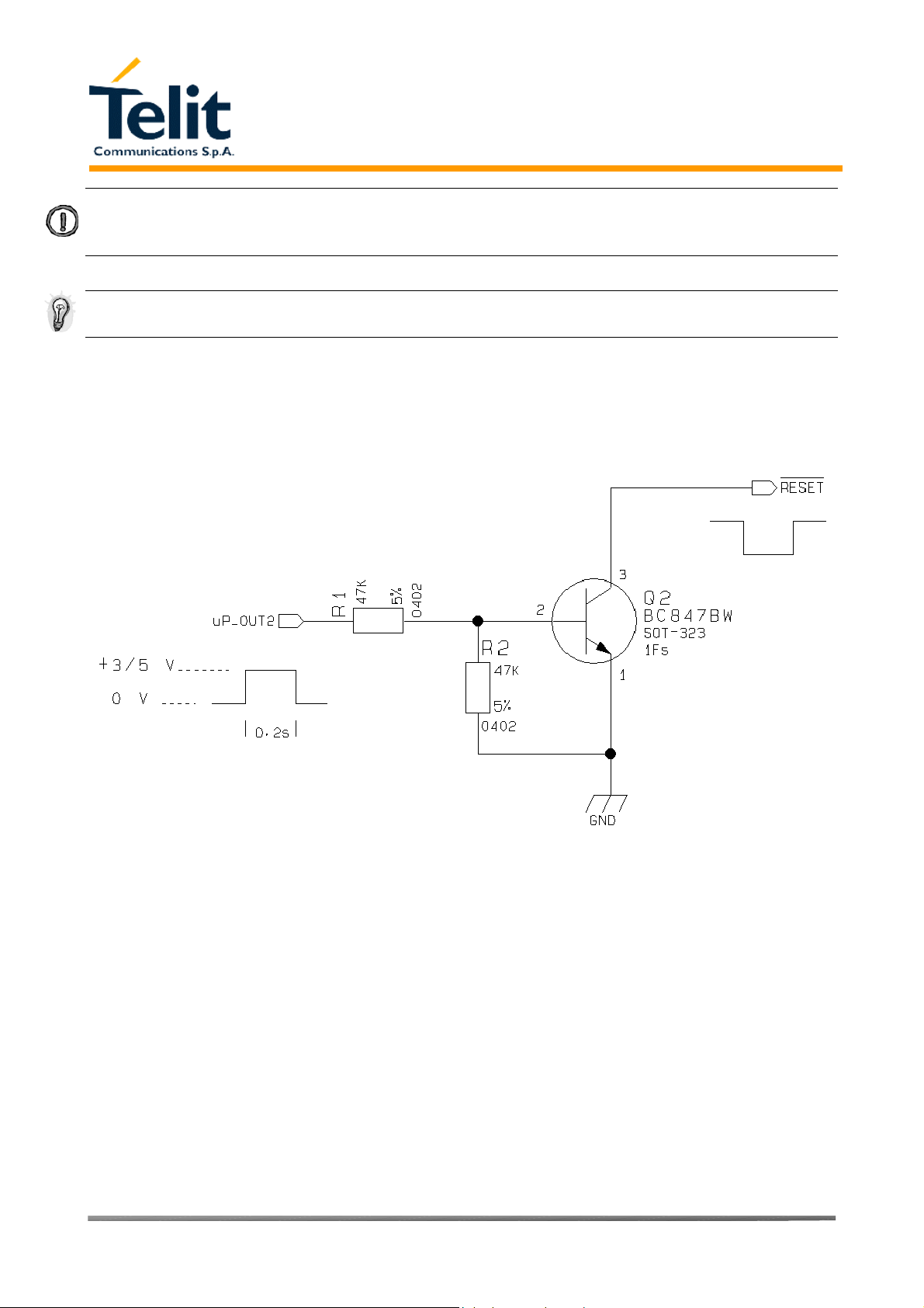
2.2.1.2 Hardware Unconditional Reset
To unconditionally turn OFF the GM862-QUAD the pin RESET# must be tied low for at least 200
milliseconds and then released.
The maximum current that can be drained from the ON# pin is 0,15 mA.
A simple circuit to do it is:
RESET#
Reproduction forbidden without DAI Telecom written authorization – All Right reserved – Right of modification reserved page 7 of 69
Unconditional Power OFF
impulse
GND
Telit GM862-QUAD/-QUAD-PY
Hardware User Guide
1vv0300692, Rev. ISSUE#0, - 04/10/2005
NOTE: don't use any pull up resistor on the RESET# line nor any totem pole digital output. Using pull
up resistor may bring to latch up problems on the GM862-QUAD power regulator and improper
functioning of the module. The line RESET# must be connected only in open collector configuration.
TIP: The unconditional hardware reset should be always implemented on the boards and software
should use it as an emergency exit procedure.
For example:
1- Let's assume you need to drive the RESET# pin with a totem pole output of a +3/5 V
microcontroller (uP_OUT2):
Unconditional Reset
impulse
Reproduction forbidden without DAI Telecom written authorization – All Right reserved – Right of modification reserved page 8 of 69

Telit GM862-QUAD/-QUAD-PY
Hardware User Guide
1vv0300692, Rev. ISSUE#0, - 04/10/2005
3 Power Supply
The power supply circuitry and board layout are the most important part in the full product design
and they strongly reflect on the product overall performances, hence read carefully the requirements
and the guidelines that will follow for a proper design.
3.1 Power Supply Requirements
The GM862-QUAD power requirements are:
• Nominal Supply Voltage: 3.8 V
• Max Supply Voltage: 4.2 V
• Supply voltage range: 3.4 V - 4.2 V
• Max Peak current consumption (impulsive): 1.9 A
• Max Average current consumption during transmission (rms): 350 mA
• Average current during Power Saving: ≈ 4 mA
• Average current during idle (Power Saving disabled) ≈ 17 mA
The GSM system is made in a way that the RF transmission is not continuous, else it is packed into
bursts at a base frequency of about 216 Hz, the relative current peaks can be as high as about 2A.
Therefore the power supply has to be designed in order to withstand with these current peaks
without big voltage drops; this means that both the electrical design and the board layout must be
designed for this current flow.
If the layout of the PCB is not well designed a strong noise floor is generated on the ground and the
supply; this will reflect on all the audio paths producing an audible annoying noise at 216 Hz; if the
voltage drop during the peak current absorption is too much, then the device may even shutdown as
a consequence of the supply voltage drop.
TIP: The electrical design for the Power supply should be made ensuring it will be capable of a peak
current output of at least 2 A.
3.2 General Design Rules
The principal guidelines for the Power Supply Design embrace three different design steps:
- the electrical design
- the thermal design.
- the PCB layout.
Reproduction forbidden without DAI Telecom written authorization – All Right reserved – Right of modification reserved page 9 of 69
Telit GM862-QUAD/-QUAD-PY
Hardware User Guide
1vv0300692, Rev. ISSUE#0, - 04/10/2005
3.2.1 Electrical design Guidelines
The electrical design of the power supply depends strongly from the power source where this power
is drained. We will distinguish them into three categories:
• +5V input (typically PC internal regulator output)
• +12V input (typically automotive)
• Battery
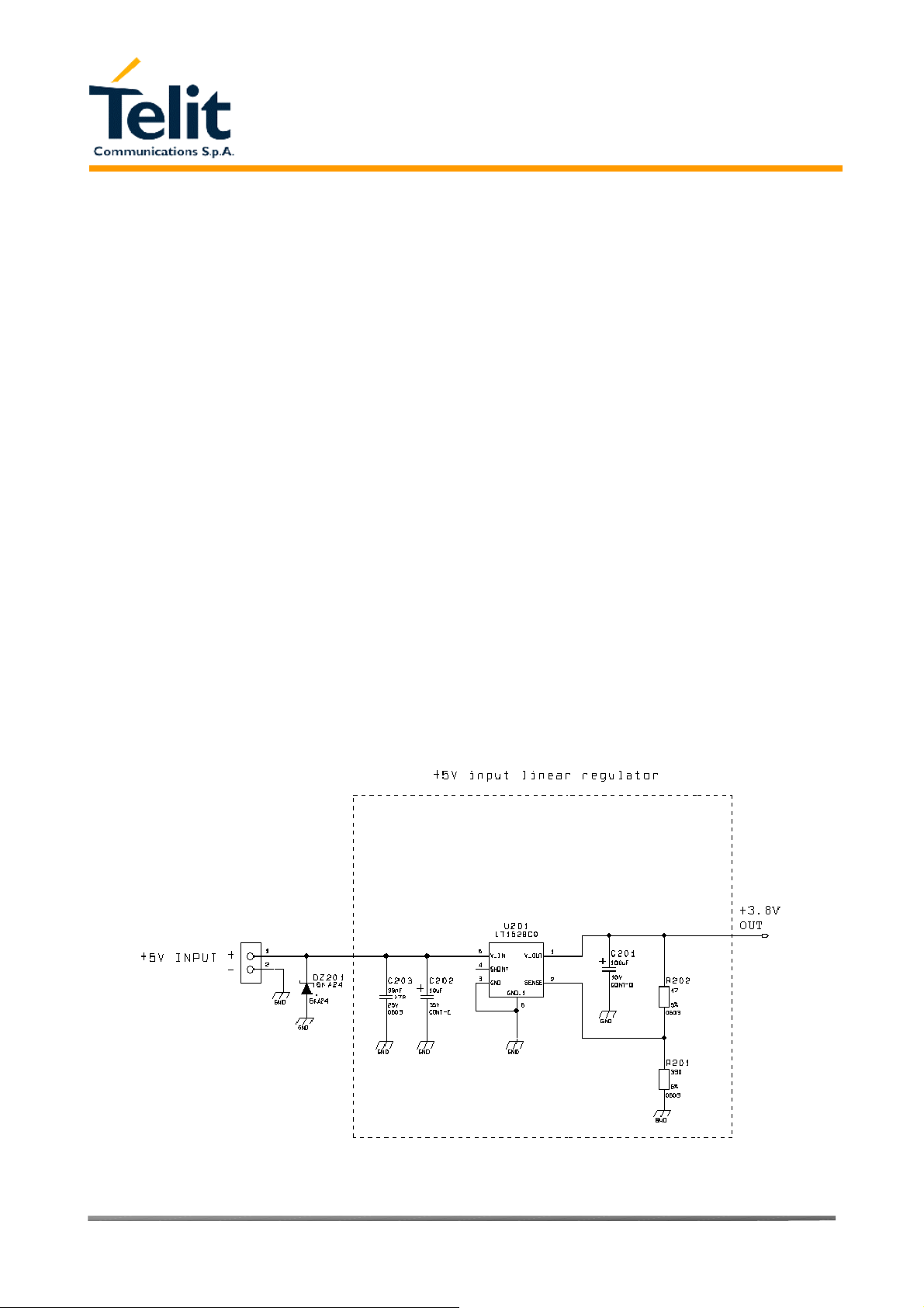
3.2.1.1 + 5V input Source Power Supply Design Guidelines
• The desired output for the power supply is 3.8V, hence there's not a big difference between the
input source and the desired output and a linear regulator can be used. A switching power
supply will not be suited because of the low drop out requirements.
• When using a linear regulator, a proper heat sink shall be provided in order to dissipate the
power generated.
• A Bypass low ESR capacitor of adequate capacity must be provided in order to cut the current
absorption peaks close to the GM862-QUAD, a 100μF tantalum capacitor is usually suited.
• Make sure the low ESR capacitor on the power supply output (usually a tantalum one) is rated
at least 10V.
• A protection diode should be inserted close to the power input, in order to save the GM862QUAD from power polarity inversion.
An example of linear regulator with 5V input is:
Reproduction forbidden without DAI Telecom written authorization – All Right reserved – Right of modification reserved page 10 of 69
Telit GM862-QUAD/-QUAD-PY
Hardware User Guide
1vv0300692, Rev. ISSUE#0, - 04/10/2005
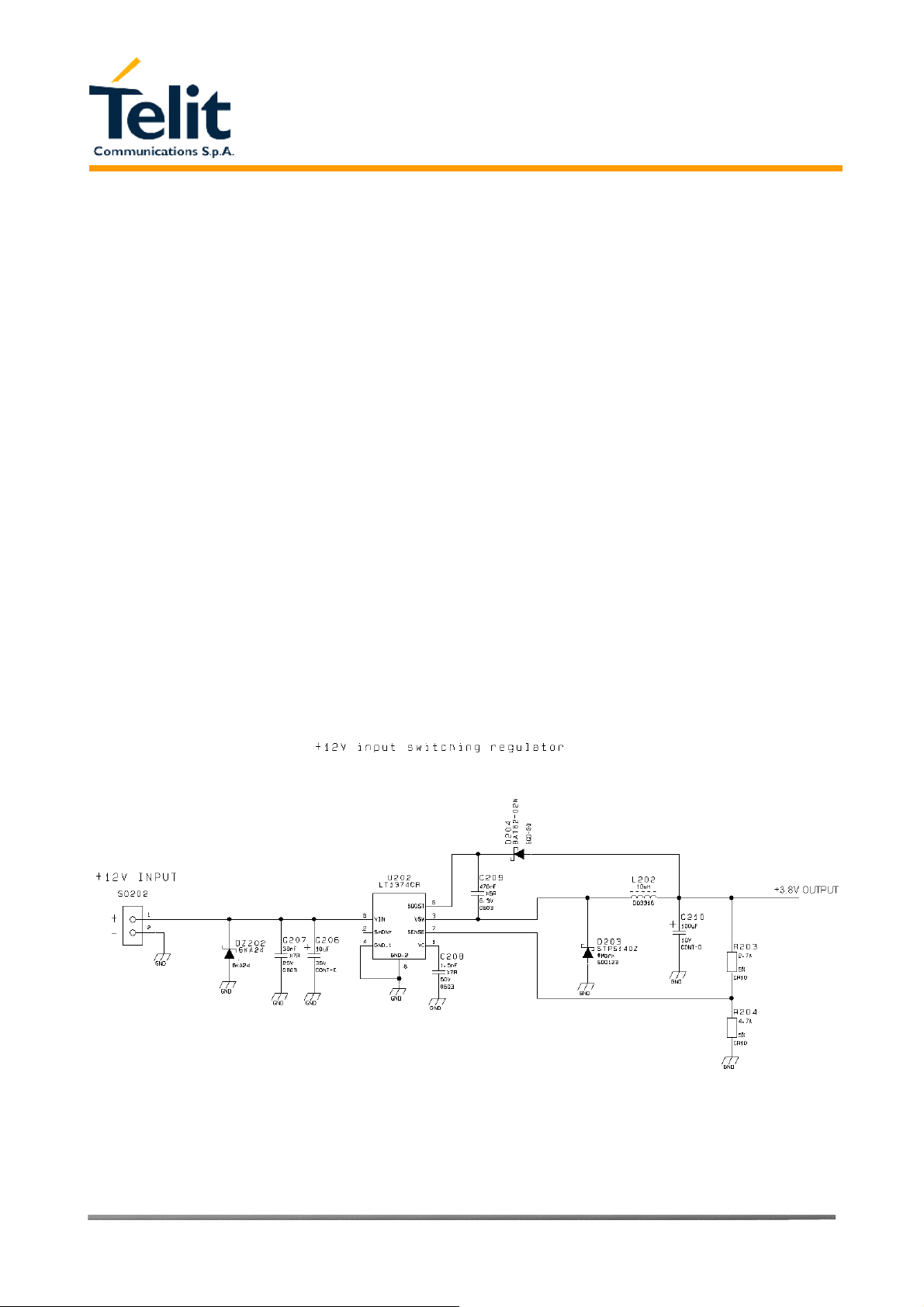
3.2.1.2 + 12V input Source Power Supply Design Guidelines
• The desired output for the power supply is 3.8V, hence due to the big difference between the
input source and the desired output, a linear regulator is not suited and shall not be used. A
switching power supply will be preferable because of its better efficiency especially with the 2A
peak current load represented by the GM862-QUAD.
• When using a switching regulator, a 500Khz switching frequency regulator is preferable
because of its smaller inductor size and its faster transient response. This allows the regulator to
respond quickly to the current peaks absorption.
• For car PB battery the input voltage can rise up to 15,8V and this should be kept in mind when
choosing components: all components in the power supply must withstand this voltage.
• A Bypass low ESR capacitor of adequate capacity must be provided in order to cut the current
absorption peaks, a 100μF tantalum capacitor is usually suited.
• Make sure the low ESR capacitor on the power supply output (usually a tantalum one) is rated
at least 10V.
• For Car applications a spike protection diode should be inserted close to the power input, in
order to clean the supply from spikes.
• A protection diode should be inserted close to the power input, in order to save the GM862QUAD from power polarity inversion. This can be the same diode as for spike protection.
An example of switching regulator with 12V input is:
Reproduction forbidden without DAI Telecom written authorization – All Right reserved – Right of modification reserved page 11 of 69

Telit GM862-QUAD/-QUAD-PY
Hardware User Guide
1vv0300692, Rev. ISSUE#0, - 04/10/2005
3.2.1.3 Battery Source Power Supply Design Guidelines
• The desired nominal output for the power supply is 3.8V and the maximum voltage allowed is
4.2V, hence a single 3.7V Li-Ion cell battery type is suited for supplying the power to the Telit
GM862-QUAD module.
The three cells Ni/Cd or Ni/MH 3,6 V Nom. battery types or 4V PB types MUST NOT BE
USED since their maximum voltage can rise over the absolute maximum voltage for the
GM862-QUAD and damage it.
NOTE: DON'T USE any Ni-Cd, Ni-MH, and Pb battery types. Their use can lead to overvoltage on the
GM862-QUAD and damage it. USE ONLY Rechargeable Li-Ion battery types.
• A Bypass low ESR capacitor of adequate capacity must be provided in order to cut the current
absorption peaks, a 100μF tantalum capacitor is usually suited.
• Make sure the low ESR capacitor (usually a tantalum one) is rated at least 10V.
• A protection diode should be inserted close to the power input, in order to save the GM862-
QUAD from power polarity inversion. Otherwise the battery connector should be done in a way
to avoid polarity inversions when connecting the battery.
• The battery capacity must be at least 500mAh in order to withstand the current peaks of 2A; the
suggested capacity is from 500mAh to 1000mAh.
3.2.1.4 Battery Charge control Circuitry Design Guidelines
The charging process for Li-Ion Batteries can be divided into 4 phases:
• Qualification and trickle charging
• Fast charge 1 - constant current
• Final charge - constant voltage or pulsed charging
• Maintenance charge
The qualification process consists in a battery voltage measure, indicating roughly its charge status.
If the battery is deeply discharged, that means its voltage is lower than the trickle charging
threshold, then the charge must start slowly possibly with a current limited pre-charging process
where the current is kept very low with respect to the fast charge value: the trickle charging.
During the trickle charging the voltage across the battery terminals rises; when it reaches the fast
charge threshold level the charging process goes into fast charge phase.
During the fast charge phase the process proceeds with a current limited charging; this current limit
depends on the required time for the complete charge and from the battery pack capacity. During
this phase the voltage across the battery terminals still raises but at a lower rate.
Reproduction forbidden without DAI Telecom written authorization – All Right reserved – Right of modification reserved page 12 of 69

Telit GM862-QUAD/-QUAD-PY
Hardware User Guide
1vv0300692, Rev. ISSUE#0, - 04/10/2005
Once the battery voltage reaches its maximum voltage then the process goes into its third state:
Final charging. The voltage measure to change the process status into final charge is very
important. It must be ensured that the maximum battery voltage is never exceeded, otherwise the
battery may be damaged and even explode. Moreover for the constant voltage final chargers, the
constant voltage phase (final charge) must not start before the battery voltage has reached its
maximum value, otherwise the battery capacity will be highly reduced.
The final charge can be of two different types: constant voltage or pulsed.
The constant voltage charge proceeds with a fixed voltage regulator (very accurately set to the
maximum battery voltage) and hence the current will decrease while the battery is becoming
charged. When the charging current falls below a certain fraction of the fast charge current value,
then the battery is considered fully charged, the final charge stops and eventually starts the
maintenance.
The pulsed charge process has no voltage regulation, instead the charge continues with pulses.
Usually the pulse charge works in the following manner: the charge is stopped for some time, let's
say few hundreds of ms, then the battery voltage will be measured and when it drops below its
maximum value a fixed time length charging pulse is issued. As the battery approaches its full
charge the off time will become longer, hence the duty-cycle of the pulses will decrease. The
battery is considered fully charged when the pulse duty-cycle is less than a threshold value,
typically 10%, the pulse charge stops and eventually the maintenance starts.
The last phase is not properly a charging phase, since the battery at this point is fully charged and
the process may stop after the final charge. The maintenance charge provides an additional charging
process to compensate for the charge leak typical of a Li-Ion battery. It is done by issuing pulses
with a fixed time length, again few hundreds of ms, and a duty-cycle around 5% or less.
This last phase is not implemented in the GM862-QUAD internal charging algorithm, so that the
battery once charged is left discharging down to a certain threshold so that it is cycled from full
charge to slight discharge even if the battery charger is always inserted. This guarantees that
anyway the remaining charge in the battery is a good percentage and that the battery is not damaged
by keeping it always fully charged (Li-Ion rechargeable battery usually deteriorate when kept fully
charged).
Last but not least, in some applications it is highly desired that the charging process restarts when
the battery is discharged and its voltage drops below a certain threshold, GM862-QUAD internal
charger does it.
As you can see, the charging process is not a trivial task to be done; moreover all these operations
should start only if battery temperature is inside a charging range, usually 5°C - 45°C.
The GM862-QUAD measures the temperature of its internal component, in order to satisfy this last
requirement, it's not exactly the same as the battery temperature but in common application the two
temperature should not differ too much and the charging temperature range should be guaranteed.
Reproduction forbidden without DAI Telecom written authorization – All Right reserved – Right of modification reserved page 13 of 69
An example of battery charger can be:
Telit GM862-QUAD/-QUAD-PY
Hardware User Guide
1vv0300692, Rev. ISSUE#0, - 04/10/2005
NOTE: In this particular application the battery charger input current must be limited to less than 1A.
This can be done by using a current limited wall adapter as the power source.
For your convenience in the EVK there's also a current unlimited input, where the input source is not
limited in current and the drawn current is limited to about 0,5A by a MOSFET in the EVK.
3.2.2Thermal Design Guidelines
The thermal design for the power supply heat sink should be done with the following specifications:
• Average current consumption during transmission @PWR level max (rms): 350mA
• Average current consumption during transmission @ PWR level min (rms): 100mA
• Average current during Power Saving: 4mA
• Average current during idle (Power Saving disabled) 17mA
NOTE: The average consumption during transmissions depends on the power level at which the
device is requested to transmit by the network. The average current consumption hence varies
significantly.
TIP: The thermal design for the Power supply should be made keeping a average consumption at the
max transmitting level during calls of 350mA rms.
Considering the very low current during idle, especially if Power Saving function is enabled, it is
possible to consider from the thermal point of view that the device absorbs current significantly
only during calls.
Reproduction forbidden without DAI Telecom written authorization – All Right reserved – Right of modification reserved page 14 of 69

Telit GM862-QUAD/-QUAD-PY
Hardware User Guide
1vv0300692, Rev. ISSUE#0, - 04/10/2005
If we assume that the device stays into transmission for short periods of time (let's say few minutes)
and then remains for a quite long time in idle (let's say one hour), then the power supply has always
the time to cool down between the calls and the heat sink could be smaller than the calculated one
for 350mA maximum RMS current, or even could be the simple chip package (no heat sink).
Moreover in the average network conditions the device is requested to transmit at a lower power
level than the maximum and hence the current consumption will be less than the 350mA, being
usually around 150mA.
For these reasons the thermal design is rarely a concern and the simple ground plane where the
power supply chip is placed can be enough to ensure a good thermal condition and avoid
overheating.
3.2.3 Power Supply PCB layout Guidelines
As seen on the electrical design guidelines the power supply shall have a low ESR capacitor on the
output to cut the current peaks and a protection diode on the input to protect the supply from spikes
and polarity inversion. The placement of these components is crucial for the correct working of the
circuitry. A misplaced component can be useless or can even decrease the power supply
performances.
• The Bypass low ESR capacitor must be placed close to the Telit GM862-QUAD power input
pins or in the case the power supply is a switching type it can be placed close to the inductor to
cut the ripple provided the PCB trace from the capacitor to the GM862-QUAD is wide enough
to ensure a dropless connection even during the 2A current peaks.
• The protection diode must be placed close to the input connector where the power source is
drained.
• The PCB traces from the input connector to the power regulator IC must be wide enough to
ensure no voltage drops occur when the 2A current peaks are absorbed. Note that this is not
made in order to save power loss but especially to avoid the voltage drops on the power line at
the current peaks frequency of 216 Hz that will reflect on all the components connected to that
supply, introducing the noise floor at the burst base frequency. For this reason while a voltage
drop of 300-400 mV may be acceptable from the power loss point of view, the same voltage
drop may not be acceptable from the noise point of view. If your application doesn't have audio
interface but only uses the data feature of the Telit GM862-QUAD, then this noise is not so
disturbing and power supply layout design can be more forgiving.
• The PCB traces to the GM862-QUAD and the Bypass capacitor must be wide enough to ensure
no voltage drops occur when the 2A current peaks are absorbed. This is for the same reason as
previous point. Try to keep this trace as short as possible.
• The PCB traces connecting the Switching output to the inductor and the switching diode must
be kept as short as possible by placing the inductor and the diode very close to the power
switching IC (only for switching power supply). This is done in order to reduce the radiated
field (noise) at the switching frequency (100-500 kHz usually).
• The use of a good common ground plane is suggested.
Reproduction forbidden without DAI Telecom written authorization – All Right reserved – Right of modification reserved page 15 of 69

Telit GM862-QUAD/-QUAD-PY
Hardware User Guide
1vv0300692, Rev. ISSUE#0, - 04/10/2005
• The placement of the power supply on the board should be done in such a way to guarantee that
the high current return paths in the ground plane are not overlapped to any noise sensitive
circuitry as the microphone amplifier/buffer or earphone amplifier.
• The power supply input cables should be kept separate from noise sensitive lines such as
microphone/earphone cables.
Reproduction forbidden without DAI Telecom written authorization – All Right reserved – Right of modification reserved page 16 of 69
Telit GM862-QUAD/-QUAD-PY
Hardware User Guide
1vv0300692, Rev. ISSUE#0, - 04/10/2005
4 Serial Port
The serial port on the Telit GM862-QUAD is the core of the interface between the module and
OEM hardware. Several configurations can be designed for the serial port on the OEM hardware,
but the most common are:
- RS232 PC com port
- microcontroller UART @ 2.8V - 3V (Universal Asynchronous Receive Transmit)
- microcontroller UART@ 5V or other voltages different from 2.8V
Depending from the type of serial port on the OEM hardware a level translator circuit may be
needed to make the system work. The only configuration that doesn't need a level translation is the
2.8V UART.
The serial port on the GM862-QUAD is a +2.8V UART with all the 7 RS232 signals. It differs
from the PC-RS232 in the signal polarity (RS232 is reversed) and levels. The levels for the GM862QUAD UART are the CMOS levels:
Absolute Maximum Ratings -Not Functional
Parameter Min Max
Input level on any
digital pin when on
Input voltage on
analog pins when on
Operating Range - Interface levels (2.8V CMOS)
Level Min Max
Input high level V
-0.3V +3.75V
-0.3V +3.0 V
2.1V 3.3V
IH
Input low level VIL 0V 0.5V
Output high level VOH2.2V 3.0V
Output low level VOL0V 0.35V
Reproduction forbidden without DAI Telecom written authorization – All Right reserved – Right of modification reserved page 17 of 69
The signals of the GM862-QUAD serial port are:
Telit GM862-QUAD/-QUAD-PY
Hardware User Guide
1vv0300692, Rev. ISSUE#0, - 04/10/2005
RS232
Pin
Number
1 DCD -
2 RXD -
3 TXD -
4 DTR -
5 GND 2-4-6-8 Ground ground
6 DSR -
7 RTS -
8 CTS -
Signal GM862-
QUAD
Pin
Number
36 Data Carrier Detect Output from the GM862-QUAD that
dcd_uart
37 Transmit line *see Note Output transmit line of GM862-QUAD
tx_uart
20 Receive line *see Note Input receive of the GM862-QUAD
rx_uart
43 Data Terminal Ready Input to the GM862-QUAD that controls
dtr_uart
33 Data Set Ready Output from the GM862-QUAD that
dsr_uart
45 Request to Send Input to the GM862-QUAD that controls
rts_uart
29 Clear to Send Output from the GM862-QUAD that
cts_uart
Name Usage
indicates the carrier presence
UART
UART
the DTE READY condition
indicates the module is ready
the Hardware flow control
controls the Hardware flow control
9 RI -
ri_uart
NOTE: According to V.24, RX/TX signal names are referred to the application side, therefore on the
GM862-QUAD side these signal are on the opposite direction: TXD on the application side will be
connected to the receive line (here named TXD/ rx_uart ) of the GM862-QUAD serial port and viceversa
for RX.
TIP: For a minimum implementation, only the TXD and RXD lines can be connected, the other lines can
be left open provided a software flow control is implemented.
The signals in the UART connector on the EVK are:
30 Ring Indicator Output from the GM862-QUAD that
indicates the incoming call condition
DCD RXD
TXD DTR
GND DSR
RTS CTS
RI GND
Reproduction forbidden without DAI Telecom written authorization – All Right reserved – Right of modification reserved page 18 of 69

Telit GM862-QUAD/-QUAD-PY
Hardware User Guide
1vv0300692, Rev. ISSUE#0, - 04/10/2005
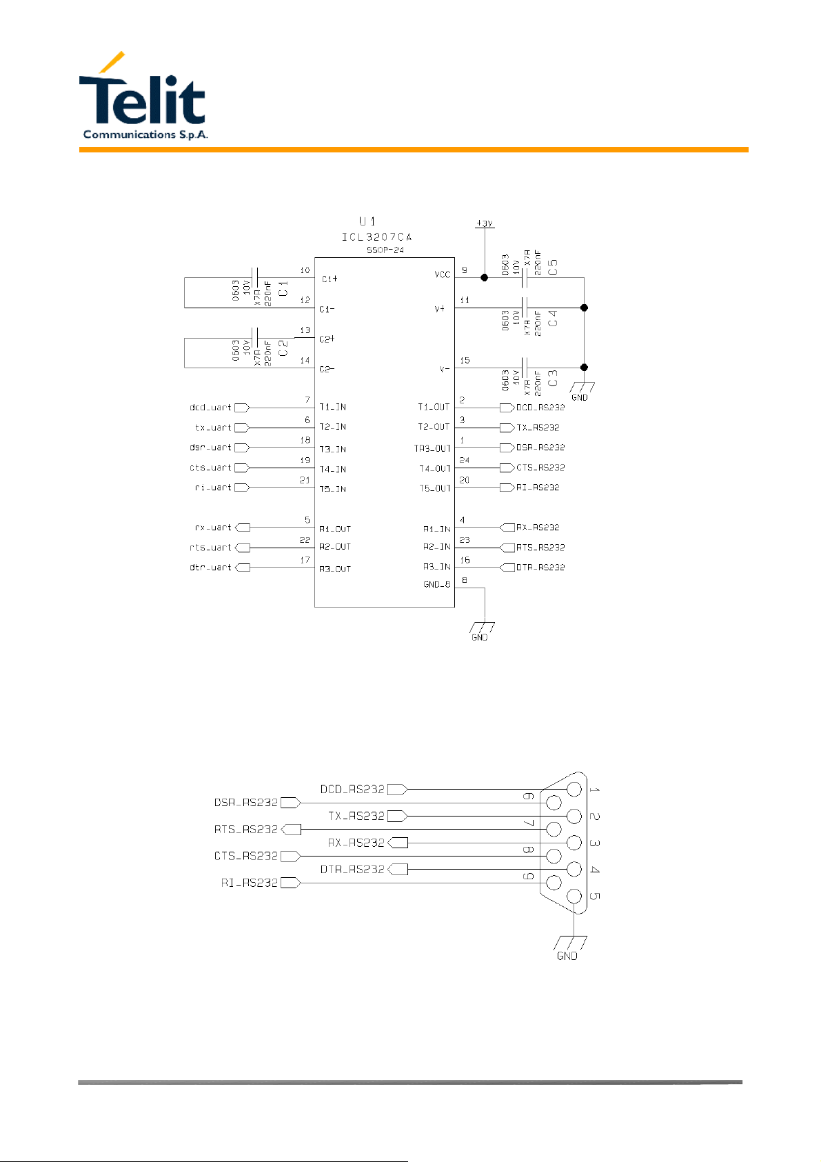
4.1 RS232 level translation
In order to interface the Telit GM862-QUAD with a PC com port or a RS232 (EIA/TIA-232)
application a level translator is required. This level translator must
- invert the electrical signal in both directions
- change the level from 0/3V to +15/-15V
Actually, the RS232 UART 16450, 16550, 16650 & 16750 chipsets accept signals with lower levels
on the RS232 side (EIA/TIA-562) , allowing for a lower voltage-multiplying ratio on the level
translator. Note that the negative signal voltage must be less than 0V and hence some sort of level
translation is always required.
The simplest way to translate the levels and invert the signal is by using a single chip level
translator. There are a multitude of them, differing in the number of driver and receiver and in the
levels (be sure to get a true RS232 level translator not a RS485 or other standards).
By convention the driver is the level translator from the 0-3V UART level to the RS232 level, while
the receiver is the translator from RS232 level to 0-3V UART.
In order to translate the whole set of control lines of the UART you will need:
- 5 driver
- 3 receiver
NOTE: The digital input lines working at 2.8VCMOS have an absolute maximum input voltage of 3,75V;
therefore the level translator IC shall not be powered by the +3.8V supply of the module. Instead it
shall be powered from a +2.8V / +3.0V (dedicated) power supply.
This is because in this way the level translator IC outputs on the module side (i.e. GM862-QUAD
inputs) will work at +3.8V interface levels, stressing the module inputs at its maximum input voltage.
This can be acceptable for evaluation purposes, but not on production devices.
Reproduction forbidden without DAI Telecom written authorization – All Right reserved – Right of modification reserved page 19 of 69
Telit GM862-QUAD/-QUAD-PY
An example of level translation circuitry of this kind is:
Hardware User Guide
1vv0300692, Rev. ISSUE#0, - 04/10/2005
the RS232 serial port lines are usually connected to a DB9 connector with the following layout:
Reproduction forbidden without DAI Telecom written authorization – All Right reserved – Right of modification reserved page 20 of 69
Telit GM862-QUAD/-QUAD-PY
Hardware User Guide
1vv0300692, Rev. ISSUE#0, - 04/10/2005
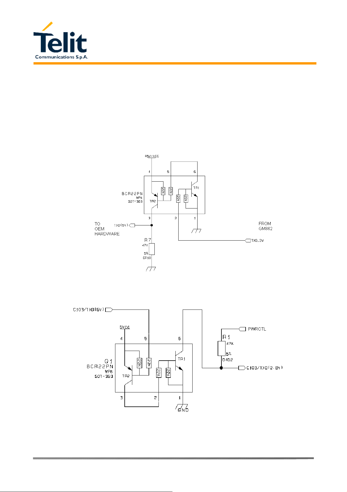
4.2 5V UART level translation
If the OEM application uses a microcontroller with a serial port (UART) that works at a voltage
different from 2.8 - 3V, then a circuitry has to be provided to adapt the different levels of the two
set of signals. As for the RS232 translation there are a multitude of single chip translators, but since
the translation requires very few components, then also a discrete design can be suited. For example
a possible inexpensive translator circuit for a 5V driver can be:
and for a 5V receiver:
Reproduction forbidden without DAI Telecom written authorization – All Right reserved – Right of modification reserved page 21 of 69
 Loading...