

Telit Communications S p A GE910G User Manual

GE910 Hardware User Guide
1vv0300962 Rev.9-bis3 – 2013-05-20
APPLICABILITY TABLE
PRODUCT
GE910-QUAD
GE910-GNSS
GE910 Hardware User Guide
GE910 Hardware User Guide
GE910 Hardware User GuideGE910 Hardware User Guide
1vv0300962 Rev.9-bis3 2013-05-20
Reproduction forbidden without Telit Communications S.p.A. written authorization - All Rights Reserved page 2 of 87
Mod. 0805 2011-07 Rev.2

GE910 Hardware User Guide
GE910 Hardware User Guide
GE910 Hardware User GuideGE910 Hardware User Guide
1vv0300962 Rev.9-bis3 2013-05-20
SPECIFICATIONS SUBJECT TO CHANGE WITHOUT NOTICE
Notice
While reasonable efforts have been made to assure the accuracy of this document, Telit assumes
no liability resulting from any inaccuracies or omissions in this document, or from use of the
information obtained herein. The information in this document has been carefully checked and is
believed to be entirely reliable. However, no responsibility is assumed for inaccuracies or
omissions. Telit reserves the right to make changes to any products described herein and
reserves the right to revise this document and to make changes from time to time in content
hereof with no obligation to notify any person of revisions or changes. Telit does not assume
any liability arising out of the application or use of any product, software, or circuit described
herein; neither does it convey license under its patent rights or the rights of others.
It is possible that this publication may contain references to, or information about Telit products
(machines and programs), programming, or services that are not announced in your country.
Such references or information must not be construed to mean that Telit intends to announce
such Telit products, programming, or services in your country.
Copyrights
This instruction manual and the Telit products described in this instruction manual may be,
include or describe copyrighted Telit material, such as computer programs stored in
semiconductor memories or other media. Laws in the Italy and other countries preserve for Telit
and its licensors certain exclusive rights for copyrighted material, including the exclusive right
to copy, reproduce in any form, distribute and make derivative works of the copyrighted
material. Accordingly, any copyrighted material of Telit and its licensors contained herein or in
the Telit products described in this instruction manual may not be copied, reproduced,
distributed, merged or modified in any manner without the express written permission of Telit.
Furthermore, the purchase of Telit products shall not be deemed to grant either directly or by
implication, estoppel, or otherwise, any license under the copyrights, patents or patent
applications of Telit, as arises by operation of law in the sale of a product.
Computer Software Copyrights
The Telit and 3rd Party supplied Software (SW) products described in this instruction manual
may include copyrighted Telit and other 3rd Party supplied computer programs stored in
semiconductor memories or other media. Laws in the Italy and other countries preserve for Telit
and other 3rd Party supplied SW certain exclusive rights for copyrighted computer programs,
including the exclusive right to copy or reproduce in any form the copyrighted computer
program. Accordingly, any copyrighted Telit or other 3rd Party supplied SW computer programs
contained in the Telit products described in this instruction manual may not be copied (reverse
engineered) or reproduced in any manner without the express written permission of Telit or the
3rd Party SW supplier. Furthermore, the purchase of Telit products shall not be deemed to grant
either directly or by implication, estoppel, or otherwise, any license under the copyrights,
patents or patent applications of Telit or other 3rd Party supplied SW, except for the normal
non-exclusive, royalty free license to use that arises by operation of law in the sale of a product.
Reproduction forbidden without Telit Communications S.p.A. written authorization - All Rights Reserved page 3 of 87
Mod. 0805 2011-07 Rev.2

GE910 Hardware User Guide
GE910 Hardware User Guide
GE910 Hardware User GuideGE910 Hardware User Guide
1vv0300962 Rev.9-bis3 2013-05-20
Usage and Disclosure Restrictions
License Agreements
The software described in this document is the property of Telit and its licensors. It is furnished
by express license agreement only and may be used only in accordance with the terms of such
an agreement.
Copyrighted Materials
Software and documentation are copyrighted materials. Making unauthorized copies is
prohibited by law. No part of the software or documentation may be reproduced, transmitted,
transcribed, stored in a retrieval system, or translated into any language or computer language,
in any form or by any means, without prior written permission of Telit
High Risk Materials
Components, units, or third-party products used in the product described herein are NOT faulttolerant and are NOT designed, manufactured, or intended for use as on-line control equipment
in the following hazardous environments requiring fail-safe controls: the operation of Nuclear
Facilities, Aircraft Navigation or Aircraft Communication Systems, Air Traffic Control, Life
Support, or Weapons Systems (High Risk Activities"). Telit and its supplier(s) specifically
disclaim any expressed or implied warranty of fitness for such High Risk Activities.
Trademarks
TELIT and the Stylized T Logo are registered in Trademark Office. All other product or service
names are the property of their respective owners.
Copyright © Telit Communications S.p.A. 2013
Reproduction forbidden without Telit Communications S.p.A. written authorization - All Rights Reserved page 4 of 87
Mod. 0805 2011-07 Rev.2

Contents
GE910 Hardware User Guide
GE910 Hardware User Guide
GE910 Hardware User GuideGE910 Hardware User Guide
1vv0300962 Rev.9-bis3 2013-05-20
1. Introduction.....................................................................................................................................................................8
1.1. Scope........................................................................................................................................................................8
1.2. Audience ..................................................................................................................................................................8
1.3. Contact Information, Support...................................................................................................................................8
1.4. Document Organization ...........................................................................................................................................9
1.5. Text Conventions ...................................................................................................................................................10
1.6. Related Documents ................................................................................................................................................10
2. Overview........................................................................................................................................................................11
3. GE910 module connections ..........................................................................................................................................12
3.1. PIN-OUT................................................................................................................................................................12
3.2. Important Pin-out to Debug in customer’s application ..........................................................................................16
3.3. LGA PADs Layout.................................................................................................................................................17
4. Hardware Commands...................................................................................................................................................18
4.1. Turning ON the GE910..........................................................................................................................................18
4.2. Turning OFF the GE910 ........................................................................................................................................22
4.3. HW Unconditional Shutdown on GE910...............................................................................................................24
5. Power Supply.................................................................................................................................................................26
5.1. Power Supply Requirements ..................................................................................................................................26
5.2. Power Consumption...............................................................................................................................................27
5.2.1.
Power consumption Plots ..............................................................................................................................28
5.3. General Design Rules.............................................................................................................................................32
5.3.1.
Electrical Design Guidelines.........................................................................................................................32
5.3.2.
Thermal Design Guidelines...........................................................................................................................35
5.3.3.
Power Supply PCB layout Guidelines ...........................................................................................................36
6. GSM Radio Section.......................................................................................................................................................38
6.1. GSM Antenna Requirements .................................................................................................................................38
6.2. GSM Antenna - PCB line Guidelines.....................................................................................................................39
6.3. PCB Guidelines in case of FCC certification.........................................................................................................40
6.3.1.
Transmission line design ...............................................................................................................................40
6.3.2.
Transmission line measurements...................................................................................................................41
6.4. GSM Antenna - Installation Guidelines.................................................................................................................43
7. Global Navigation Satellite System (GE910-GNSS)...................................................................................................44
7.1. Principles of operation ...........................................................................................................................................44
7.2. GNSS Signals Pinout .............................................................................................................................................45
7.3. Turning ON/OFF the GNSS module only in standalone mode..............................................................................45
7.4. RF Front End Design..............................................................................................................................................45
7.4.1.
RF Signal Requirements ................................................................................................................................46
7.4.2.
GNSS Antenna – PCB Line Guidelines .........................................................................................................46
7.4.3.
GNSS Antenna Polarization ..........................................................................................................................46
7.4.4.
GNSS Antenna Gain ......................................................................................................................................48
7.4.5.
Active versus Passive Antenna ......................................................................................................................48
7.4.6.
RF Trace Losses ............................................................................................................................................49
7.4.7.
Implications of the Pre-select SAW Filter.....................................................................................................49
Reproduction forbidden without Telit Communications S.p.A. written authorization - All Rights Reserved page 5 of 87
Mod. 0805 2011-07 Rev.2

GE910 Hardware User Guide
GE910 Hardware User Guide
GE910 Hardware User GuideGE910 Hardware User Guide
1vv0300962 Rev.9-bis3 2013-05-20
7.4.8.
External LNA Gain and Noise Figure...........................................................................................................49
7.4.9.
Powering the External LNA (active antenna)................................................................................................49
7.4.10. External LNA Enable.....................................................................................................................................50
8. Logic Level Specifications ............................................................................................................................................51
9. USB Port........................................................................................................................................................................52
9.1. USB 2.0 FS ............................................................................................................................................................52
10. Serial Ports................................................................................................................................................................53
10.1. Modem Serial Port .................................................................................................................................................53
10.2. RS232 level translation ..........................................................................................................................................56
11. Audio Section Overview...........................................................................................................................................58
11.1. Digital Voice Interface (DVI) ................................................................................................................................58
11.1.1. DVI Electrical Connections...........................................................................................................................58
11.2. Analog Front-End...................................................................................................................................................58
11.2.1. MIC connection .............................................................................................................................................58
11.2.2. LINE-IN connection.......................................................................................................................................60
11.2.3. EAR connection .............................................................................................................................................61
11.2.4. Electrical Characteristics..............................................................................................................................63
12. General Purpose I/O.................................................................................................................................................65
12.1. Using a GPIO Pad as INPUT .................................................................................................................................66
12.2. Using a GPIO Pad as OUTPUT .............................................................................................................................66
12.3. Indication of network service availability..............................................................................................................67
12.4. RTC Bypass out .....................................................................................................................................................68
12.5. External SIM Holder Implementation....................................................................................................................68
12.6. ADC Converter ......................................................................................................................................................68
12.6.1. Description....................................................................................................................................................68
12.6.2. Using ADC Converter ...................................................................................................................................68
13. Mounting the GE910 on your Board.......................................................................................................................69
13.1. General...................................................................................................................................................................69
13.2. Module finishing & dimensions.............................................................................................................................69
13.3. Recommended foot print for the application..........................................................................................................70
13.4. Stencil.....................................................................................................................................................................71
13.5. PCB pad design......................................................................................................................................................71
13.6. Recommendations for PCB pad dimensions..........................................................................................................71
13.7. Solder paste............................................................................................................................................................73
13.7.1. GE910 Solder reflow .....................................................................................................................................73
14. Packing system..........................................................................................................................................................75
14.1. Packing on Reel......................................................................................................................................................75
14.1.1. Carrier Tape Detail.......................................................................................................................................75
14.1.2. Reel Detail.....................................................................................................................................................76
14.1.3. Packaging Detail...........................................................................................................................................77
14.2. Packing on tray.......................................................................................................................................................78
14.3. Moisture sensibility................................................................................................................................................80
15. Conformity Assessment Issues.................................................................................................................................81
16. SAFETY RECOMMANDATIONS.........................................................................................................................86
Reproduction forbidden without Telit Communications S.p.A. written authorization - All Rights Reserved page 6 of 87
Mod. 0805 2011-07 Rev.2

GE910 Hardware User Guide
GE910 Hardware User Guide
GE910 Hardware User GuideGE910 Hardware User Guide
1vv0300962 Rev.9-bis3 2013-05-20
17. Document History.....................................................................................................................................................87
Reproduction forbidden without Telit Communications S.p.A. written authorization - All Rights Reserved page 7 of 87
Mod. 0805 2011-07 Rev.2
1. Introduction
1.1. Scope
The aim of this document is the description of some hardware solutions useful for developing a
product with the Telit GE910 module.
1.2. Audience
This document is intended for Telit customers, who are integrators, about to implement their
applications using our GE910 modules.
1.3. Contact Information, Support
For general contact, technical support, to report documentation errors and to order manuals,
contact Telit’s Technical Support Centre (TTSC) at:
TS-EMEA@telit.com
TS-NORTHAMERICA@telit.com
TS-LATINAMERICA@telit.com
TS-APAC@telit.com
Alternatively, use:
http://www.telit.com/en/products/technical-support-center/contact.php
For detailed information about where you can buy the Telit modules or for recommendations on
accessories and components visit:
http://www.telit.com
To register for product news and announcements or for product questions contact Telit’s
Technical Support Centre (TTSC).
Our aim is to make this guide as helpful as possible. Keep us informed of your comments and
suggestions for improvements.
Telit appreciates feedback from the users of our information.
GE910 Hardware User Guide
GE910 Hardware User Guide
GE910 Hardware User GuideGE910 Hardware User Guide
1vv0300962 Rev.9-bis3 2013-05-20
Reproduction forbidden without Telit Communications S.p.A. written authorization - All Rights Reserved page 8 of 87
Mod. 0805 2011-07 Rev.2
1.4. Document Organization
This document contains the following chapters:
Chapter 1: “Introduction” provides a scope for this document, target audience, contact and
support information, and text conventions.
Chapter 2: “Overview” provides an overview of the document.
Chapter 3: “GE910 Module Connections” deals with the pin out configuration and layout.
Chapter 4: “Hardware Commands” How to operate on the module via hardware.
Chapter 5: “Power supply” Power supply requirements and general design rules.
Chapter 6: “GSM Radio” The antenna connection and board layout design are the most
important parts in the full product design.
Chapter 7: “GNSS Receiver” This section describes the GNSS receiver.
Chapter 8: “Logic Level specifications” Specific values adopted in the implementation of logic
levels for this module.
Chapter 9: “USB Port” Describes the USB port and the interface between the module and OEM
hardware.
Chapter 10: “Serial ports” Describes the UART ports present and the interface between the
module and OEM hardware.
Chapter 11: “Audio Section overview” Refers to the audio blocks of the Base Band Chip of the
GE910 Telit Modules.
Chapter 12: “General Purpose I/O” How the general purpose I/O pads can be configured.
Chapter 13: “Mounting the GE910 on the application board” Recommendations and specifics on
how to mount the module on the user’s board.
Chapter 14: “Packing system” Packaging Information.
Chapter 15: “Conformity Assessment Issues” Information related to the Conformity
Assessments.
Chapter 16: “Safety Recommendations” Information related to the Safety topics.
Chapter 17: “Document History”
GE910 Hardware User Guide
GE910 Hardware User Guide
GE910 Hardware User GuideGE910 Hardware User Guide
1vv0300962 Rev.9-bis3 2013-05-20
Reproduction forbidden without Telit Communications S.p.A. written authorization - All Rights Reserved page 9 of 87
Mod. 0805 2011-07 Rev.2
1.5. Text Conventions
Danger – This information MUST be followed or catastrophic equipment failure or bodily
injury may occur.
Caution or Warning – Alerts the user to important points about integrating the module, if
these points are not followed, the module and end user equipment may fail or malfunction.
Tip or Information – Provides advice and suggestions that may be useful when integrating
the module.
All dates are in ISO 8601 format, i.e. YYYY-MM-DD.
GE910 Hardware User Guide
GE910 Hardware User Guide
GE910 Hardware User GuideGE910 Hardware User Guide
1vv0300962 Rev.9-bis3 2013-05-20
1.6. Related Documents
• Telit 's GSM/GPRS Family Software User Guide, 1vv0300784
• Audio settings application note , 80000NT10007a
• Digital Voice Interface Application Note, 80000NT10004a
• GE910 Product description, 80397ST10107A
• SIM Holder Design Guides, 80000NT10001a
• AT Commands Reference Guide, 80000ST10025a
• Telit EVK2 User Guide, 1vv0300704
Reproduction forbidden without Telit Communications S.p.A. written authorization - All Rights Reserved page 10 of 87
Mod. 0805 2011-07 Rev.2
2. Overview
The aim of this document is the description of some hardware solutions useful for developing a
product with the Telit GE910 module.
In this document all the basic functions of a mobile phone will be taken into account; for each
one of them a proper hardware solution will be suggested and eventually the wrong solutions
and common errors to be avoided will be evidenced. Obviously this document cannot embrace
the whole hardware solutions and products that may be designed. The wrong solutions to be
avoided shall be considered as mandatory, while the suggested hardware configurations shall not
be considered mandatory, instead the information given shall be used as a guide and a starting
point for properly developing your product with the Telit GE910 module. For further hardware
details that may not be explained in this document refer to the Telit GE910 Product Description
document where all the hardware information is reported.
NOTICE:
(The integration of the GSM/GPRS GE910 cellular module within user application shall be
done according to the design rules described in this manual.
The information presented in this document is believed to be accurate and reliable. However, no
responsibility is assumed by Telit Communications S.p.A. for its use, nor any infringement of
patents or other rights of third parties which may result from its use. No license is granted by
implication or otherwise under any patent rights of Telit Communications S.p.A. other than for
circuitry embodied in Telit products. This document is subject to change without notice.
GE910 Hardware User Guide
GE910 Hardware User Guide
GE910 Hardware User GuideGE910 Hardware User Guide
1vv0300962 Rev.9-bis3 2013-05-20
Reproduction forbidden without Telit Communications S.p.A. written authorization - All Rights Reserved page 11 of 87
Mod. 0805 2011-07 Rev.2
3. GE910 module connections
3.1. PIN-OUT
GE910 Hardware User Guide
GE910 Hardware User Guide
GE910 Hardware User GuideGE910 Hardware User Guide
1vv0300962 Rev.9-bis3 2013-05-20
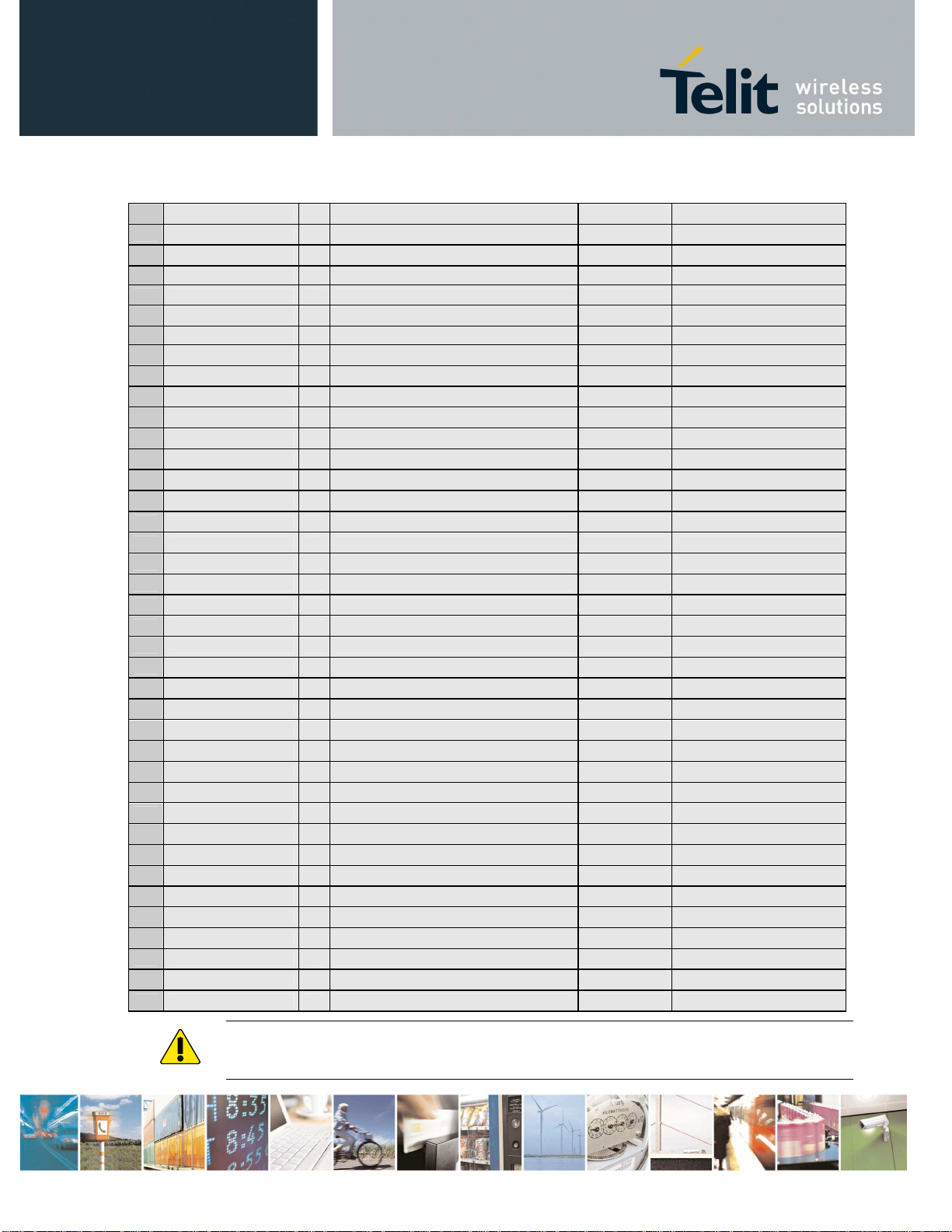
PAD
USB 2.0 COMMUNICATION PORT
B15
C15
A13
Asynchronous UART1 – Program / Data + HW Flow Control
N15
M15
M14
L14
P15
N14
P14
R14
Asynchronous Auxiliary UART2
D15
E15
SIM card interface
A6
A7
A5
A4
A3
Analog Voice Interface
B2
B3
B4
B5
Digital Voice Interface (DVI)
B9
B6
B7
B8
ADC
B1
DIGITAL IO
C8
Signal I/O Function Type COMMENT
USB_D+ I/O USB differential Data (+) 3.3V
USB_D- I/O USB differential Data (-) 3.3V
VUSB AI Power sense for USB presence 5V Accepted range 1.8V to 5V
C103/TXD I Serial data input from DTE CMOS 1.8V UART1
C104/RXD O Serial data output to DTE CMOS 1.8V UART1
C108/DTR I Input for (DTR) from DTE CMOS 1.8V
C105/RTS I Input for Request to send signal (RTS) from DTE CMOS 1.8V
C106/CTS O Output for Clear to Send signal (CTS) to DTE
C109/DCD O Output for (DCD) to DTE CMOS 1.8V
C107/DSR O Output for (DSR) to DTE CMOS 1.8V
C125/RING O Output for Ring (RI) to DTE CMOS 1.8V
TX_AUX O Auxiliary UART (TX Data to DTE) CMOS 1.8V UART2
RX_AUX I Auxiliary UART (RX Data from DTE) CMOS 1.8V UART2
SIMCLK O External SIM signal – Clock 1.8 / 3V
SIMRST O External SIM signal – Reset 1.8 / 3V
SIMIO I/O External SIM signal – Data I/O 1.8 / 3V
SIMIN I External SIM signal – Presence (active low) CMOS 1.8
SIMVCC - External SIM signal – Power supply for the SIM 1.8 / 3V
EAR+ AO Ear signal output, phase +
EAR- AO Ear signal output, phase -
MIC+ AI Microphone signal input; phase +
MIC- AI Microphone signal input; phase -
DVI_WA0 I/O Digital Audio Interface (WA0) CMOS 1.8V
DVI_RX I/O Digital Audio Interface (RX) CMOS 1.8V
DVI_TX I/O Digital Audio Interface (TX) CMOS 1.8V
DVI_CLK I/O Digital Audio Interface (CLK) CMOS 1.8V
ADC_IN1 AI Analog to Digital converter input A/D Values 0 to 1.3V
GPIO_01 I/O GPIO_01 / STAT_LED CMOS 1.8V Alternate Function STATUS LED
CMOS 1.8V
Reproduction forbidden without Telit Communications S.p.A. written authorization - All Rights Reserved page 12 of 87
Mod. 0805 2011-07 Rev.2
GE910 Hardware User Guide
GE910 Hardware User Guide
GE910 Hardware User GuideGE910 Hardware User Guide
1vv0300962 Rev.9-bis3 2013-05-20
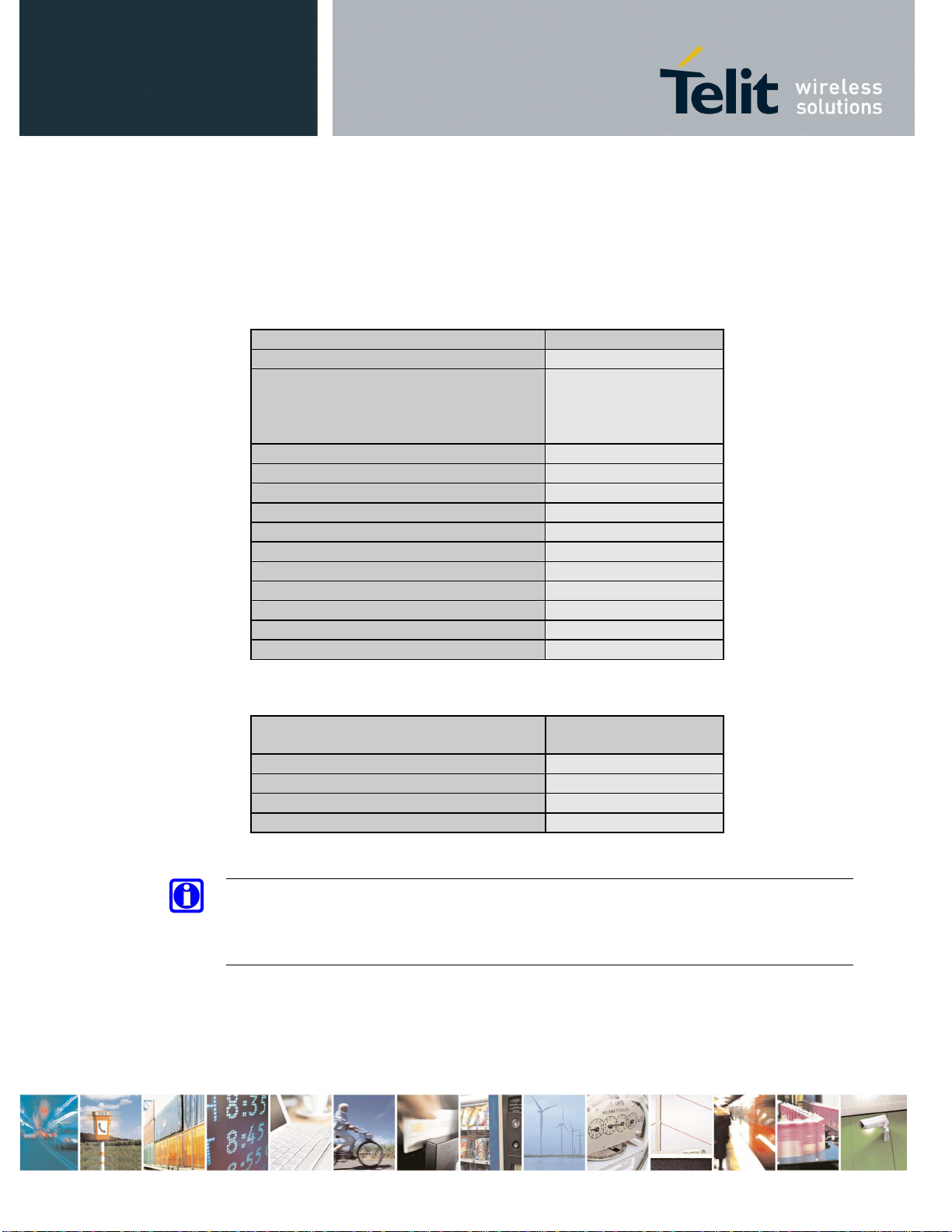
C9
C10
C11
B14
C12
C13
K15
L15
G15 GPIO_10 I/O GPIO_10 CMOS 1.8V
RF SECTION GSM
K1
GNSS SECTION
R9
G14
J14
K14
R7 GNSS_LNA_EN O GNSS External LNA Enable 1.8V Active Antenna Control
MISCELLANEOUS
FUNCTIONS
R13
P11
R12
C14
R11
POWER SUPPLY
M1
M2
N1
N2
P1
P2
E1
G1
H1
J1
L1
A2
E2
F2
G2
H2
GPIO_02 I/O GPIO_02 CMOS 1.8V
GPIO_03 I/O GPIO_03 CMOS 1.8V
GPIO_04 I/O GPIO_04 CMOS 1.8V
GPIO_05 I/O GPIO_05 / RFTXMON CMOS 1.8V Alternate Function RFTXMON
GPIO_06 I/O GPIO_06 CMOS 1.8V
GPIO_07 I/O GPIO_07 CMOS 1.8V
GPIO_08 I/O GPIO_08 CMOS 1.8V
GPIO_09 I/O GPIO_09 CMOS 1.8V
ANTENNA GSM - GSM/GPRS Antenna (50 ohm) RF
ANTENNA GNSS - GNSS Antenna (50 ohm) RF
GNSS_EN* I External GNSS ON-OFF VBATT ref. Open Colector active low
GNSS_NMEA_TX O UART NMEA Output 1.8V UART3 or GNSS_BOOT
GNSS_NMEA_RX I UART NMEA Input 1.8V UART3
HW_SHUTDOWN* I HW Unconditional Shutdown VBATT ref. Open Colector active low
RESET_BB I SW Reset 1.8V Open Colector active low
ON_OFF* I Input command for power ON VRTC 2,3V ref. Open Colector active low
VRTC I VRTC Backup capacitor RTC Power
VAUX/PWRMON O
VBATT - Main power supply (Baseband) Power
VBATT - Main power supply (Baseband) Power
VBATT_PA - Main power supply (Radio PA) Power
VBATT_PA - Main power supply (Radio PA) Power
VBATT_PA - Main power supply (Radio PA) Power
VBATT_PA - Main power supply (Radio PA) Power
GND - Ground Power
GND - Ground Power
GND - Ground Power
GND - Ground Power
GND - Ground Power
GND - Ground Power
GND - Ground Power
GND - Ground Power
GND - Ground Power
GND - Ground Power
Supply Output for external accessories / Power
ON Monitor
1.8V
Backup for the embedded RTC
supply, don’t connect to VBATT!
Reproduction forbidden without Telit Communications S.p.A. written authorization - All Rights Reserved page 13 of 87
Mod. 0805 2011-07 Rev.2
GE910 Hardware User Guide
GE910 Hardware User Guide
GE910 Hardware User GuideGE910 Hardware User Guide
1vv0300962 Rev.9-bis3 2013-05-20
J2
K2
L2
R2
M3
N3
P3
R3
M4
N4
P4
R4
N5
P5
R5
N6
P6
R6
P8
R8
P9
P10
R10
M12
B13
P13
E14
RESERVED
C1
P7
D1
C2
D2
C3
D3
E3
F3
G3
H3
J3
K3
L3
GND - Ground Power
GND - Ground Power
GND - Ground Power
GND - Ground Power
GND - Ground Power
GND - Ground Power
GND - Ground Power
GND - Ground Power
GND - Ground Power
GND - Ground Power
GND - Ground Power
GND - Ground Power
GND - Ground Power
GND - Ground Power
GND - Ground Power
GND - Ground Power
GND - Ground Power
GND - Ground Power
GND - Ground Power
GND - Ground Power
GND - Ground Power
GND - Ground Power
GND - Ground Power
GND - Ground Power
GND - Ground Power
GND - Ground Power
GND - Ground Power
RESERVED - RESERVED
RESERVED - RESERVED
RESERVED - RESERVED
RESERVED - RESERVED
RESERVED - RESERVED
RESERVED - RESERVED
RESERVED - RESERVED
RESERVED - RESERVED
RESERVED - RESERVED
RESERVED - RESERVED
RESERVED - RESERVED
RESERVED - RESERVED
RESERVED - RESERVED
RESERVED - RESERVED
Reproduction forbidden without Telit Communications S.p.A. written authorization - All Rights Reserved page 14 of 87
Mod. 0805 2011-07 Rev.2
GE910 Hardware User Guide
GE910 Hardware User Guide
GE910 Hardware User GuideGE910 Hardware User Guide
1vv0300962 Rev.9-bis3 2013-05-20
C4
C5
C6
C7
N7
N8
N9
A10
N10
N11
B12
D12
N12
P12
F14
H14
N13
L13
J13
M13
K13
H13
G13
F13
A11
A12
B11
B10
A9
A8
A14
D13
D14
H15
J15
F1
D4
E13
F15
RESERVED - RESERVED
RESERVED - RESERVED
RESERVED - RESERVED
RESERVED - RESERVED
RESERVED - RESERVED
RESERVED - RESERVED
RESERVED - RESERVED
RESERVED - RESERVED
RESERVED - RESERVED
RESERVED - RESERVED
RESERVED - RESERVED
RESERVED - RESERVED
RESERVED - RESERVED
RESERVED - RESERVED
RESERVED - RESERVED
RESERVED - RESERVED
RESERVED - RESERVED
RESERVED - RESERVED
RESERVED - RESERVED
RESERVED - RESERVED
RESERVED - RESERVED
RESERVED - RESERVED
RESERVED - RESERVED
RESERVED - RESERVED
RESERVED - RESERVED
RESERVED - RESERVED
RESERVED - RESERVED
RESERVED - RESERVED
RESERVED - RESERVED
RESERVED - RESERVED
RESERVED - RESERVED
RESERVED - RESERVED
RESERVED - RESERVED
RESERVED - RESERVED
RESERVED - RESERVED
RESERVED - RESERVED
RESERVED - RESERVED
RESERVED - RESERVED
RESERVED - RESERVED
WARNING:
Reserved pins must not be connected.
Reproduction forbidden without Telit Communications S.p.A. written authorization - All Rights Reserved page 15 of 87
Mod. 0805 2011-07 Rev.2
GE910 Hardware User Guide
GE910 Hardware User Guide
GE910 Hardware User GuideGE910 Hardware User Guide
1vv0300962 Rev.9-bis3 2013-05-20
3.2. Important Pin-out to Debug in customer’s application
The followings pins are necessary to debug the application when the module is assembled on
customer’s application.
PADs for GE910-QUAD Signal
M1,M2,N1,N2,P1,P2 VBATT & VBATT_PA
E1,G1,H1,J1,L1,A2,E2,F2,G2,H2,
J2,K2,L2,R2,M3,N3,P3,R3,M4,
N4,P4,R4,N5,P5,R5,N6,P6,R6,P8,
R8,P9,P10,R10,M12,B13,P13,E14
ADDITIONAL PADs
for GE910-GNSS only
We recommend connecting them also to dedicated test point.
GND
R12 ON/OFF*
R13 HW_SHUTDOWN*
K1 ANTENNA GSM
B15 USB_D+
C15 USB_DN15 C103/TXD
M15 C104/RXD
L14 C105/RTS
P15 C106/CTS
D15 TXD_AUX
E15 RXD_AUX
Signal
R9 ANTENNA GNSS
G14 GNSS_EN*
J14 GNSS_NMEA_TX
K14 GNSS_NMEA_RX
NOTE:
Not used pins apart from table above can be left unconnected.
RTS pin should be connected to the GND (on the module side) if flow control is not used.
Reproduction forbidden without Telit Communications S.p.A. written authorization - All Rights Reserved page 16 of 87
Mod. 0805 2011-07 Rev.2
3.3. LGA PADs Layout
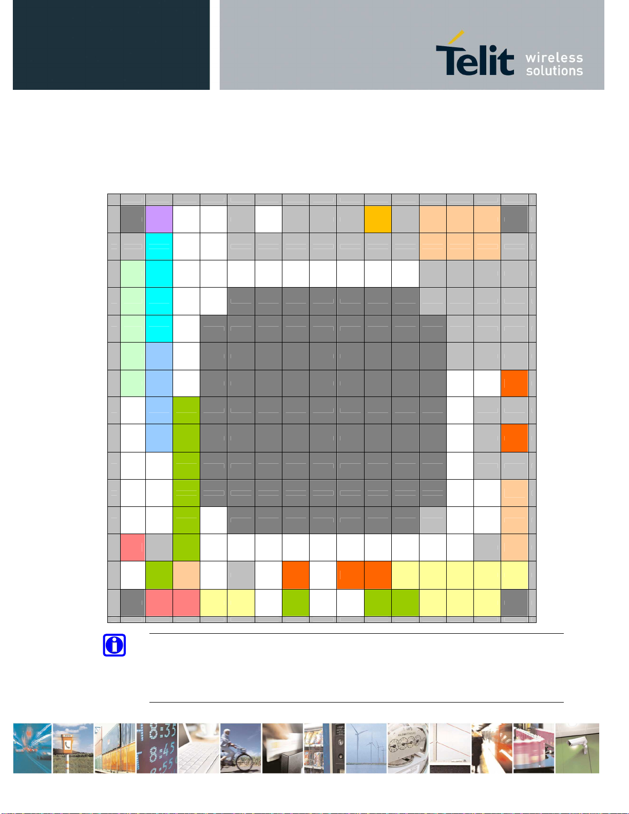
A B C D E F G H J K L M N P R
1 ADC IN1 RES RES GND RES GND GND GND ANT_GSM GND VBATT VBATT_PA VBATT_PA
2 GND EAR+ RES RES GND GND GND GND G ND GND GND VBATT VBATT_PA VBATT_PA GND
3 SIMVCC EAR- RES RES RES RES RES RES RES RES RES GND GND GND GND
4 SIMIN MIC+ RES RES GND GND GND GND
5 SIMIO MIC- RES GND GND GND
TOP VIEW
GE910 Hardware User Guide
GE910 Hardware User Guide
GE910 Hardware User GuideGE910 Hardware User Guide
1vv0300962 Rev.9-bis3 2013-05-20
6 SIMCLK DVI_RX RES GND GND GND
7 SIMRST DVI_TX RES RES RES
8 RES DVI_CLK GPIO_01 RES GND GND
9 RES DVI_WA0 GPIO_02 RES GND ANT_GNSS
10 RES RES GPIO_03 RES GND GND
11 RES RES GPIO_04 RES RES
12 RES RES GPIO_06 RES GN D RES RES ON_OFF*
USB
13
14 RES GP IO_05 VRTC RES GND RES GNSS_E N* RES
15 USB_D+ USB_ D- TX AUX RX A UX RES GPIO_10 RES RES GPIO_08 GPIO_09 C104/RXD C103/TXD C106/CTS
GND GP IO_07 RES RES RES RES RES RES RES RES RES RES GND
_VBUS
GNSS
GNSS
_NMEA_TX
C105/RTS C108/DTR C109/DCD C107/DSR C125/RING
_NMEA_RX
NOTE:
GNSS
_LNA_EN
VAUX /
PWRMON
HW_SHUT
DOWN*
The pin defined as RES has to be considered RESERVED and not connected on any pin in the
application. The related area on the application has to be kept empty.
Pin G14; J14; K14; R7; R9 are available only on GE910-GNSS variant.
Reproduction forbidden without Telit Communications S.p.A. written authorization - All Rights Reserved page 17 of 87
Mod. 0805 2011-07 Rev.2
4. Hardware Commands
4.1. Turning ON the GE910
To turn on the GE910 the pad ON-OFF* must be tied low for at least 5 seconds and then
released.
The maximum current that can be drained from the ON-OFF* pad is 0.2mA.
NOTE:
Don't use any pull up resistor on the ON* line, it is internally pulled up. Using pull up resistor
may bring to latch up problems on the GE910 power regulator and improper power on/off of the
module. The line ON* must be connected only in open collector configuration.
GE910 Hardware User Guide
GE910 Hardware User Guide
GE910 Hardware User GuideGE910 Hardware User Guide
1vv0300962 Rev.9-bis3 2013-05-20
NOTE:
In this document all the lines that are inverted, hence have active low signals are labeled with a
name that ends with”*" or with a bar over the name.
TIP:
To check if the device has powered on, the hardware line PWRMON should be monitored. The
device is powered on when PWRMON goes high.
NOTE:
It is mandatory to avoid sending data to the serial ports during the first 200ms of the module
start-up.
Reproduction forbidden without Telit Communications S.p.A. written authorization - All Rights Reserved page 18 of 87
Mod. 0805 2011-07 Rev.2
Y
N
HW un
conditional
Y
N
GE910 Hardware User Guide
GE910 Hardware User Guide
GE910 Hardware User GuideGE910 Hardware User Guide
1vv0300962 Rev.9-bis3 2013-05-20
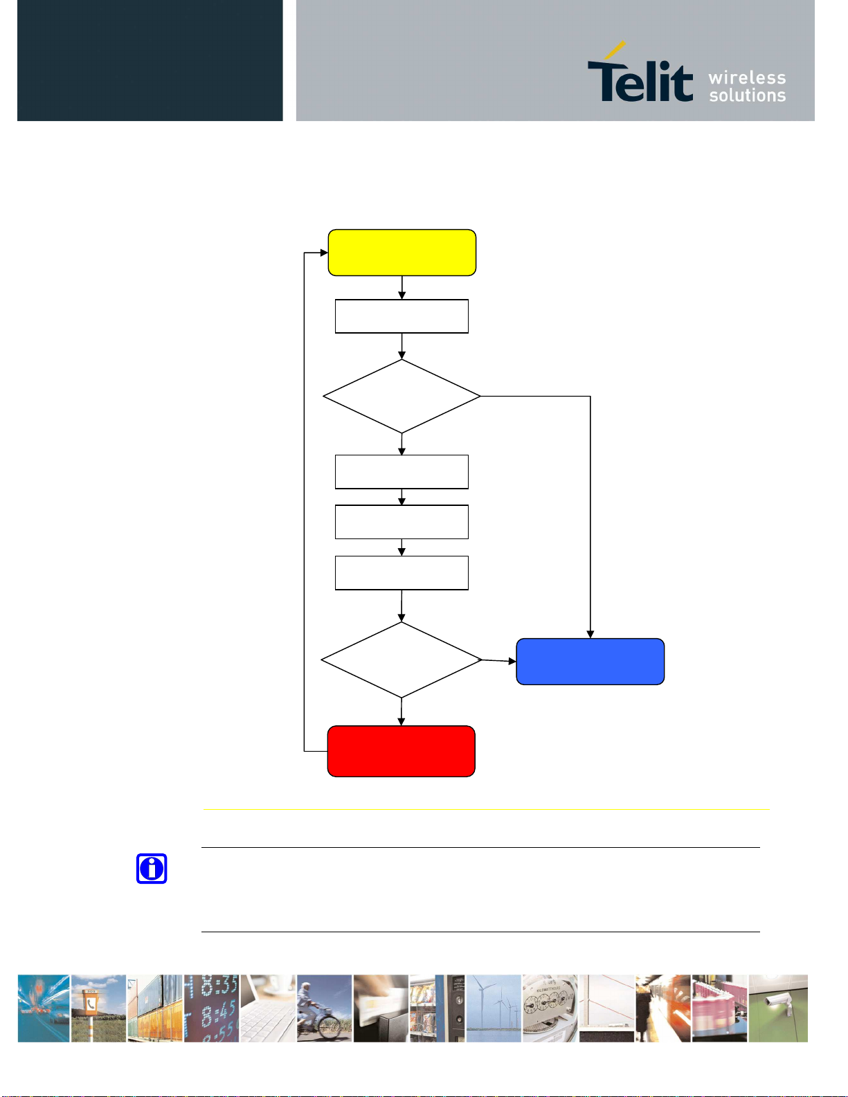
The flow chart showing the proper TURN ON procedure is displayed below:
MODEM ON Proc.
WAIT > 1 Sec
PWMON HIGH?
NOTE:
ON_OFF = LOW
WAIT > 5 Sec
ON_OFF = Z
PWMON HIGH?
SHUTDOWN
Start AT CMD.
In order to avoid a back powering effect it is recommended to avoid having any HIGH logic
level signal applied to the digital pins of the GE910 when the module is powered off or during
an ON/OFF transition.
Reproduction forbidden without Telit Communications S.p.A. written authorization - All Rights Reserved page 19 of 87
Mod. 0805 2011-07 Rev.2
AT init s
equence
HW
unconditional
GE910 Hardware User Guide
GE910 Hardware User Guide
GE910 Hardware User GuideGE910 Hardware User Guide
1vv0300962 Rev.9-bis3 2013-05-20
The Flow chart showing the AT commands managing procedure is displayed below:
Start AT CMD.
DELAY > 300msec
Enter AT<CR>
AT answer ‘OK’
into 1 sec ?
N
SHUTDOWN
MODEM ON Proc.
Y
.
NOTE:
Do not give any commands before 300 msec after ON/OFF procedure.
Reproduction forbidden without Telit Communications S.p.A. written authorization - All Rights Reserved page 20 of 87
Mod. 0805 2011-07 Rev.2
GE910 Hardware User Guide
GE910 Hardware User Guide
GE910 Hardware User GuideGE910 Hardware User Guide
1vv0300962 Rev.9-bis3 2013-05-20
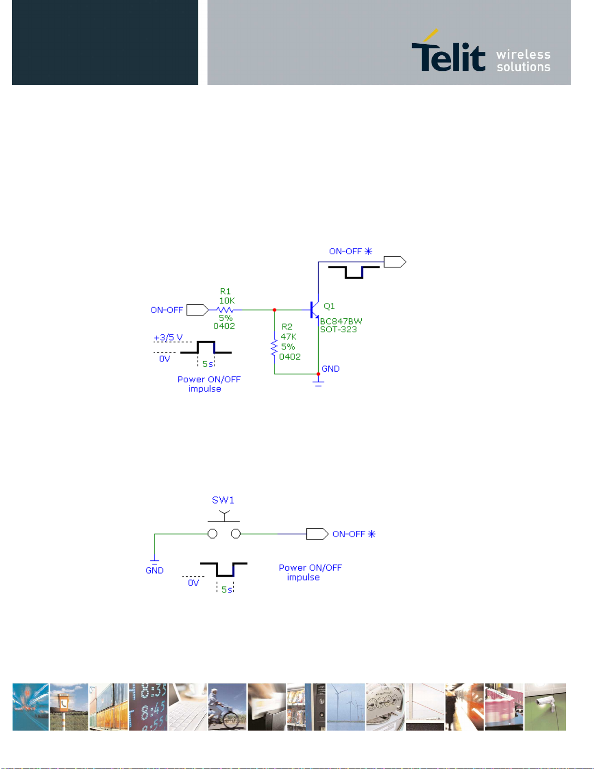
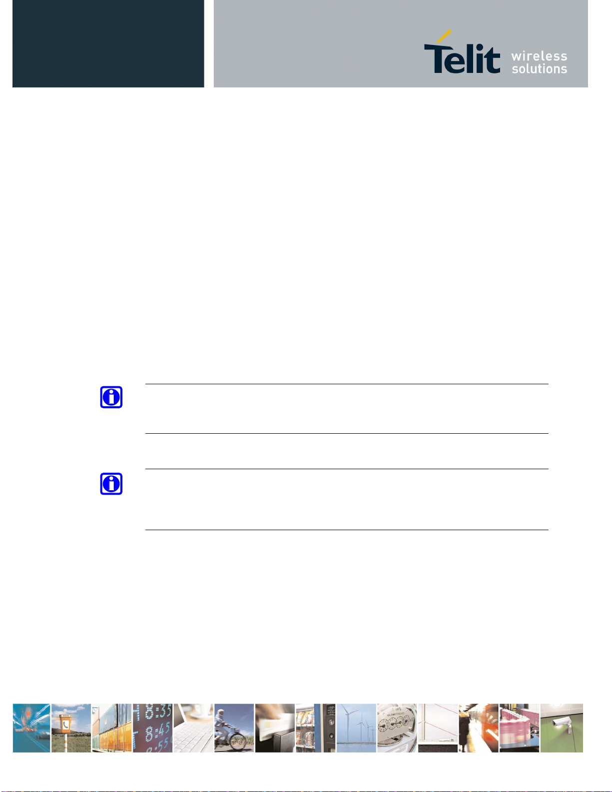
ON-OFF Circuit Examples:
1- If your system does not have Open Collector bus, use this interface:
2- Using a simple ON/OFF external switch:
Reproduction forbidden without Telit Communications S.p.A. written authorization - All Rights Reserved page 21 of 87
Mod. 0805 2011-07 Rev.2
4.2. Turning OFF the GE910
Turning OFF of the device can be done in two ways:
• via AT command (see GE910 Software User Guide, AT#SHDN)
• by tying low pin ON_OFF* for at least 2s
Either ways, the device issues a detach request to network informing that the device will not
be reachable any more.
To turn OFF the GE910 the pad ON-OFF* must be tied low for at least 2 seconds and then
released.
The same circuitry and timing for the power on must be used.
The device shuts down after the release of the ON-OFF* pad.
GE910 Hardware User Guide
GE910 Hardware User Guide
GE910 Hardware User GuideGE910 Hardware User Guide
1vv0300962 Rev.9-bis3 2013-05-20
TIP:
To check if the device has been powered off, the hardware line PWRMON must be monitored.
The device is powered off when PWRMON goes low.
NOTE:
In order to avoid a back powering effect it is recommended to avoid having any HIGH logic
level signal applied to the digital pins of the GE910 when the module is powered off or during
an ON/OFF transition.
Reproduction forbidden without Telit Communications S.p.A. written authorization - All Rights Reserved page 22 of 87
Mod. 0805 2011-07 Rev.2
N
Y
HW unconditional
N
Y
GE910 Hardware User Guide
GE910 Hardware User Guide
GE910 Hardware User GuideGE910 Hardware User Guide
1vv0300962 Rev.9-bis3 2013-05-20
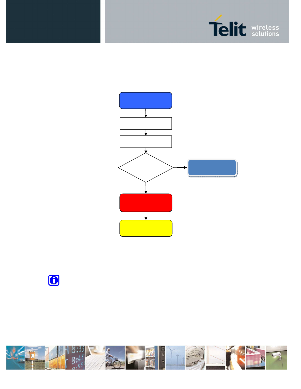
The following flow chart shows the proper HW TURN OFF procedure:
MODEM OFF Proc.
WAIT > 1 Sec
PWMON HIGH?
ON_OFF = LOW
WAIT > 2s
ON_OFF = Z
WAIT > 15s
PWMON HIGH?
SHUTDOWN
MODEM ON Proc.
Reproduction forbidden without Telit Communications S.p.A. written authorization - All Rights Reserved page 23 of 87
Mod. 0805 2011-07 Rev.2
4.3. HW Unconditional Shutdown on GE910
WARNING:
The hardware unconditional Shutdown must not be used during normal operation of the device
since it does not detach the device from the network. It shall be kept as an emergency exit
procedure to be done in the rare case that the device gets stacked waiting for some network or
SIM responses.
To unconditionally Shutdown the GE910, the pad HW_SHUTDOWN* must be tied low for at
least 200 milliseconds and then released. After this operation the module is in OFF condition.
The maximum current that can be drained from the HW_SHUTDOWN* pad is 0,4 mA.
NOTE:
GE910 Hardware User Guide
GE910 Hardware User Guide
GE910 Hardware User GuideGE910 Hardware User Guide
1vv0300962 Rev.9-bis3 2013-05-20
Do not use any pull up resistor on the HW_SHUTDOWN* line or any totem pole digital output.
Using pull up resistor may bring to latch up problems on the GE910 power regulator and
improper functioning of the module. The line HW_SHUTDOWN* must be connected only in
open collector configuration, since it is already internally pull-up to VBATT.
TIP:
The unconditional hardware shutdown must always be implemented on the boards and the
software must use it as an emergency exit procedure.
A simple circuit to do it is:
Reproduction forbidden without Telit Communications S.p.A. written authorization - All Rights Reserved page 24 of 87
Mod. 0805 2011-07 Rev.2
HW
unconditional
Disconnect PWR
GE910 Hardware User Guide
GE910 Hardware User Guide
GE910 Hardware User GuideGE910 Hardware User Guide
1vv0300962 Rev.9-bis3 2013-05-20
In the following flow chart is detailed the proper HW restart procedure:
SHUTDOWN
HW SHUTDOWN* =
Delay > 200ms
HW SHUTDOWN* =
PWRMON = HIGH
Y
supply
LOW
Z
N
Modem ON Proc.
NOTE:
In order to avoid a back powering effect it is recommended to avoid having any HIGH logic
level signal applied to the digital pins of the GE910 when the module is powered off or during
an ON/OFF transition.
Reproduction forbidden without Telit Communications S.p.A. written authorization - All Rights Reserved page 25 of 87
Mod. 0805 2011-07 Rev.2
5. Power Supply
The power supply circuitry and board layout are a very important part in the full product design
and they strongly reflect on the product overall performances, hence read carefully the
requirements and the guidelines that will follow for a proper design.
5.1. Power Supply Requirements
The external power supply must be connected to VBATT & VBATT_PA signals and must
fulfill the following requirements:
POWER SUPPLY
Nominal Supply Voltage 3.8 V
Normal Operating Voltage Range 3.40 V÷ 4.20 V
Extended Operating Voltage Range 3.20 V÷ 4.50 V
GE910 Hardware User Guide
GE910 Hardware User Guide
GE910 Hardware User GuideGE910 Hardware User Guide
1vv0300962 Rev.9-bis3 2013-05-20
NOTE:
The Operating Voltage Range MUST never be exceeded; care must be taken in order to fulfil
min/max voltage requirement.
NOTE:
Overshoot voltage (regarding MAX Extended Operating Voltage) and drop in voltage
(regarding MIN Extended Operating Voltage) MUST never be exceeded;
The “Extended Operating Voltage Range” can be used only with completely assumption and
application of the HW User guide suggestions.
Reproduction forbidden without Telit Communications S.p.A. written authorization - All Rights Reserved page 26 of 87
Mod. 0805 2011-07 Rev.2
GE910 Hardware User Guide
GE910 Hardware User Guide
GE910 Hardware User GuideGE910 Hardware User Guide
1vv0300962 Rev.9-bis3 2013-05-20
5.2. Power Consumption
The GE910 power consumptions are:
GE910
Mode Average (mA) @3.8V Mode description
GSM+GNSS SWITCHED OFF
Switched Off 100uA
GSM mode only
IDLE mode
AT+CFUN=1 21 Normal mode: full functionality of the module
AT+CFUN=4
18 Disabled TX and RX; module is not registered
3,8 Paging Multiframe 2
AT+CFUN=0 or =5
2,5 Paging Multiframe 3
2,4 Paging Multiframe 4
1,2 Paging Multiframe 9
VOICE TX and RX mode
GSM900 VOICE PL5 230
DCS1800 VOICE PL0 175
GPRS (class 1) 1TX + 1RX
GSM900 PL5 225
DCS1800 PL0 160
GPRS (class 10) 2TX + 3RX
GSM900 PL5 360
DCS1800 PL0 290
GNSS mode only
Tracking GPS 55
Tracking GNSS 65
The GSM system is made in a way that the RF transmission is not continuous, else it is packed
into bursts at a base frequency of about 216 Hz, and the relative current peaks can be as high as
about 2A. Therefore the power supply has to be designed in order to withstand with these
current peaks without big voltage drops; this means that both the electrical design and the board
layout must be designed for this current flow.
If the layout of the PCB is not well designed a strong noise floor is generated on the ground and
the supply; this will reflect on all the audio paths producing an audible annoying noise at 216
Hz; if the voltage drop during the peak current absorption is too much, then the device may even
shutdown as a consequence of the supply voltage drop.
Module supplied but Switched Off
on the network
GSM VOICE CALL
GPRS Sending data mode
GPRS Sending data mode
NOTE:
The electrical design for the Power supply should be made ensuring it will be capable of a peak
current output of at least 2 A.
Reproduction forbidden without Telit Communications S.p.A. written authorization - All Rights Reserved page 27 of 87
Mod. 0805 2011-07 Rev.2
 Loading...