

PRECISION TEMPERA TURE-
V
CC
V
CC
V
OUT
V
OUT
GND
GND
TC02VNB
TC03VNB
TC02VZB
TC03VZB
11223
3
PRELIMINARY INFORMATION
TO -VOL T AGE CONVERTERS
PRECISION TEMPERATURE-TO-VOL TAGE CONVERTERS
TC02
TC02
TC03
TC03
FEATURES
■ Linearized Temperature-to-Voltage Converters
■ Direct Centigrade Output Voltage Scaling (TC03)
■ Wide Temperature Measurement
Range (TC02) ............................... – 20°C to +125°C
■ Excellent Temperature Converter Linearity .. 0.8°C
Over Temperature
■ High Temperature Converter Accuracy..........±2°C
at 25°C Guaranteed
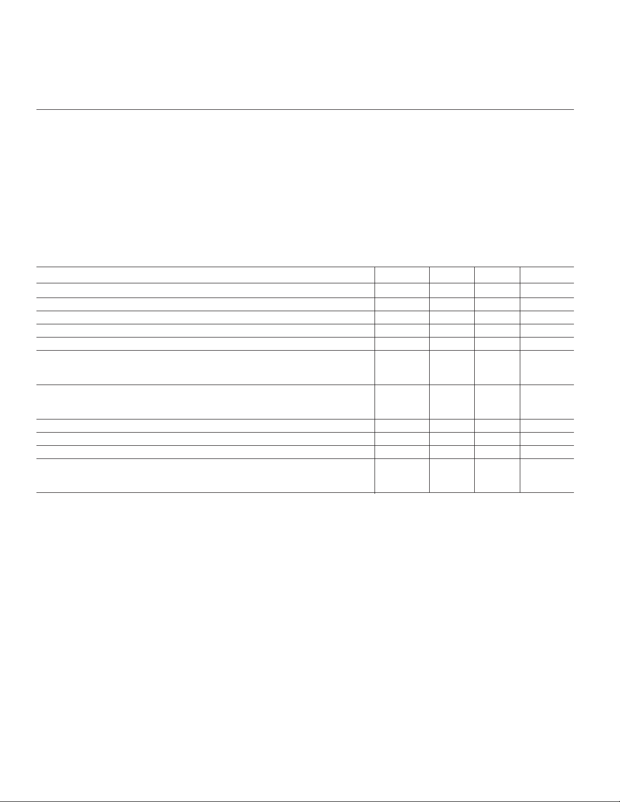
■ Small Packages ................TO-92-3 and SOT-23B-3
APPLICATIONS
■ Power Supply Thermal Shut-Down
■ Temperature-Controlled Fans
■ Temperature Measurement/Instrumentation
■ Temperature Regulators
■ Consumer Electronics
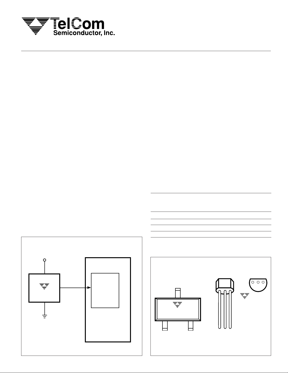
FUNCTIONAL BLOCK DIAGRAM
GENERAL DESCRIPTION
The TC02/03 temperature sensors furnish a linearized
output voltage directly proportional to measured temperature. The TC03 has a temperature measurement range of
– 20°C to +100°C. Its output voltage is directly calibrated in
degrees Centigrade (i.e. V
= 10mV/°C x Temperature
OUT
°C). An external pull-down resistor to a negative voltage
source is required for temperature measurement below
0°C.
The TC02 has a temperature measurement range of
– 20°C to +125°C, and operates with a single supply. It has
the same output voltage slope with temperature as the
TC03 (10mV/°C). The output voltage range is 300mV at
– 20°C to 1,750mV at +125°C.
Small size, low cost and low power operation make the
TC02/03 suitable for a wide range of general purpose
temperature measurement applications.
ORDERING INFORMATION
Output
Voltage
Part No. Package At 25°C Temp. Range
TC02VNB *SOT-23B-3 750mV – 20°C to +125°C
TC02VZB TO-92 750mV – 20°C to +125°C
TC03VNB *SOT-23B-3 250mV – 20°C to +100°C
TC03VZB TO-92 250mV – 20°C to +100°C
NOTE: *SOT-23B-3 is equivalent to JEDEC (TO-236)
VCC = 2.2V to 12V
TC02/03-04 6/18/97
MICROCONTROLLER
V
CC
V
OUT
TC03
GND
TelCom Semiconductor reserves the right to make changes in the circuitry and specifications of its devices.
A/D
CONVERTER
1
PIN CONFIGURATION
.
*SOT-23B-3
(Top View)
NOTE: *SOT-23B-3 is equivalent
to JEDEC (TO-236)
TO-92-3
PRELIMINARY INFORMATION
TC02
TC03
PRECISION TEMPERATURE-
TO -VOL T AGE CONVERTERS
ABSOLUTE MAXIMUM RATINGS *
Supply Voltage ............................................................15V
Input Voltage, Any Terminal..............– 1.0 to (VCC +0.3V)
Operating Temperature (TC02).............– 20°C to +125°C
Operating Temperature (TC03).............– 20°C to +100°C
Storage Temperature ............................– 55°C to +150°C
Lead Temperature (Soldering, 10 sec)
* Static-sensitive device. Unused devices must be stored in conductive
material. Protect devices from static discharge and static fields. Stresses
above those listed under Absolute Maximum Ratings may cause permanent damage to the device. These are stress ratings only and functional
operation of the device at these or any other conditions above those
indicated in the operational sections of the specifications is not implied.
Exposure to Absolute Maximum Rating Conditions for extended periods
may affect device reliability.
SOT-23B-3 .....................................................+260°C
TO-92-3 .......................................................... +300°C
ELECTRICAL CHARACTERISTICS :
Symbol Parameter Test Conditions Min Typ Max Unit
V
CC
V
CC
I
S
I
SRC
A
V
V
OUTMAX
Supply Voltage (TC02) 3.0 — 12 V
Supply Voltage (TC03) 2.2 — 12 V
Supply Current Note 1 — 40 60 µA
V
Output Source Current — — 1.0 mA
OUT
Accuracy at Room Temperature
Accuracy at Minimum Temperature TC02: TA = – 20°C– 7± 0.5 +5 °C
Accuracy at Maximum Temperature TC02: TA = +125°C – 3 — +3 °C
(Note 2)
Nonlinearity Note 3, 4 – 0.8 — +0.8 °C
Line Regulation — 80 — µV/V
Average Slope of Output Voltage — 10 — mV/°C
Maximum Output Voltage
TA = – 20°C to +125°C, VCC = 5V ±5%,
TA = 25°C (Note 2) – 2 ± 0.5 +2 °C
TC03: T
(Note 2)
TC03: T
TC02: 3.0V ≤ VCC ≤ 12V
TC03: 2.2V ≤ VCC ≤ 12V
(Note 1)
= – 20°C– 7± 0.5 +5
A
= +100°C – 3 — +3
A
unless otherwise specified.
——V
– 1.2 V
CC
Notes: 1. V
2. Accuracy = Difference between calculated output voltage (10mV/°C x Device case temperature at specified temperature and power supply)
DETAILED DESCRIPTION
A plot of output voltage versus temperature for both the
TC02 and TC03 appears in Figure 1. The TC03 can be
used with single power supply to measure temperatures
from 0°C to 100°C. A pull-down resistor (R1 in Figure 2)
must be added from V
measuring temperatures less than 0°C. The value of the
resistor must be chosen to limit the maximum current
pulled from the output to the negative supply to
outputs open circuited.
OUT
and measured output voltage expressed in °C.
3. Nonlinearity = deviation of output voltage versus temperature from the best-fit straight line over the device rated temperature range.
4. Guaranteed by design.
OUTPUT STAGE
Both the TC02 and TC03 have Class A output stages
capable of sourcing 1mA. These devices have a limited
ability to drive heavy capacitive loads. Loads of 50pF (to
ground) can be driven directly. For heavier loads, a 2kΩ (or
to the negative power supply for
OUT
greater) resistor should be placed in series with the output
for decoupling. If the TC02/03 is used in a noisy electrical
environment, a 0.1µF bypass capacitor from VCC to GND is
recommended.
– 50µA (i.e. R1 = VSS/50µA).
TC02/03-04 6/18/97
2

PRECISION TEMPERA TURETO -VOL T AGE CONVERTERS
1.8
1.7
1.6
1.5
1.4
1.3
1.2
1.1
1.0
0.9
(VOLTS)
0.8
0.7
OUT
V
0.6
0.5
0.4
0.3
0.2
0.1
0
– 0.1
– 0.2
– 40
TC02: V
TC03: V
– 30 – 20
= (10mV/°C) (Temperature °C) + 500mV
OUT
= (10mV/°C) (Temperature °C)
OUT
TC02
–10
0
10
20
30
TC03
40
PRELIMINARY INFORMATION
50
60 70 80 90 100 110 120
TC02
TC03
130
TEMPERATURE (°C)
Figure 1. Output Voltage vs Temperature
= 2.2V to 12.0V MIN.
V
CC
V
CC
V
GND
OUT
R1
V
SS
TC03
TC03 (– 20°C to +100°C)
Figure 2. TC02/03 Power Supply Connections for Full Scale Measurements
V
OUT
R1 = VSS/50µA
V
CC
TC02 (– 20°C to +125°C)
= 3.0V to 12.0V
V
CC
V
OUT
TC02
GND
V
OUT
TC02/03-04 6/18/97
3

PRELIMINARY INFORMATION
TC02
TC03
TYPICAL CHARACTERISTICS
PRECISION TEMPERATURE-
TO -VOL T AGE CONVERTERS
SUPPLY CURRENT (µA)
100
80
60
40
20
10
125
100
75
50
Supply Current vs.
Temperature
VCC= +5V
–50
–25 0 25 50 75 100 125
TEMPERATURE (°C)
Thermal Response
in Still Air vs.Time
Thermal Time Constant
(Sec) vs. Air Velocity
60
50
40
30
20
10
THERMAL TIME (SEC)
0
0
AIR VELOCITY (FPM)
V
(From Power Initially Applied)
OUT
vs. Time (Turn-on Response)
2V/DIV
0V
400 600 800 1000200
25
PERCENT OF FINAL VALUE (%)
0
0
20
60 80 100
40
TIME (SEC.)
500mV/DIV
0V
20µsec/DIV
TC02/03-04 6/18/97
4

PRECISION TEMPERA TURETO -VOL T AGE CONVERTERS
MARKING
PRELIMINARY INFORMATION
TC02
TC03
SOT-23B-3
a & b = part number code and temperature range
TC02VNB = AA – 20°C to 125°C
TC03VNB = AB – 20°C to 100°C
ex: 02 = uuuu
ex: 03 = uuuu
A A
A B
c = year and quarter
d = lot ID
TAPING FORMS
TO-92-3
4
5
3
2
1
9
10
8
7
6
14
15
13
12
11
a & b = TC (fixed)
c, d & e = blank
f, g, h & i = part number
j = temperature range
C = – 20°C to +125°C
D = – 20°C to +100°C
k, l, m, n & o = traceability code
SOT-23B-3
PIN 1
PIN 1
Device
Marking
User Direction of Feed
Standard Reel Component Orientation
for 713 or TR Suffix Device
(Mark Right Side Up)
Marking
Device
Reverse Reel Component Orientation
for 723 or RT Suffix Device
(Mark Upside Down)
User Direction of Feed
P
Tape & Reel Specifications Table
Package Carrier Width (W) Pitch (P) Part Per Full Reel Reel Size
3L SOT-23B 8 mm 4 mm 3000 7
W
TC02/03-04 6/18/97
5

PRELIMINARY INFORMATION
TC02
TC03
TAPING FORMS (Cont.)
Mark
Face
M
ARK
F
ACE
Seal
Tape
PRECISION TEMPERATURE-
TO -VOL T AGE CONVERTERS
Component Taping Orientation for TO-92
User Direction of Feed
P
M
ARK
F
ACE
M
ARK
F
ACE
Back
Tape
Back
Tape
Mark
Face
Seal
Tape
WW
User Direction of Feed
P
M
ARK
F
ACE
M
ARK
F
ACE
M
ARK
F
ACE
Tape & Reel Specifications Table
Package Carrier Width (W) Pitch (P) Part Per Full Reel Reel Size
TO-92-3 18 mm 12.7 mm 2000 13
TC02/03-04 6/18/97
Standard Reel Component Orientation
for 713 or TR Suffix Device
Reverse Reel Component Orientation
for 723 or RT Suffix Device
6

PRECISION TEMPERA TURETO -VOL T AGE CONVERTERS
PACKAGE DIMENSIONS
PRELIMINARY INFORMATION
TC02
TC03
*SOT-23B-3
.021 (0.54)
.015 (0.37)
.103 (2.64)
.083 (2.10)
.040 (0.60)
.017 (0.44)
.120 (3.05)
.105 (2.67)
.040 (1.02)
.031 (0.79)
.004 (0.10)
.001(0.02)
*NOTE: SOT-23B-3 is equivalent to JEDEC (TO-236)
.210 (5.33)
.170 (4.32)
.080 (2.05)
.070 (1.78)
.500
(12.70)
MIN.
.055 (1.40)
.047 (1.20)
8° MAX.
TO-92-3
.007 (0.18)
.003 (0.085)
.010 (0.25)
.005 (0.13)
.165 (4.19)
.125 (3.18)
.105 (2.67)
.080 (2.03)
.205 (5.21)
.175 (4.45)
Sales Offices
TelCom Semiconductor
1300 Terra Bella Avenue
P.O. Box 7267
Mountain View, CA 94039-7267
TEL: 415-968-9241
FAX: 415-967-1590
E-Mail: liter@c2smtp.telcom-semi.com
TC02/03-04 6/18/97
.018 (0.46)
.015 (0.38)
TelCom Semiconductor
Austin Product Center
9101 Burnet Rd. Suite 214
Austin, TX 78758
TEL: 512-873-7100
FAX: 512-873-8236
.055 (1.40)
.045 (1.14)
.105 (2.67)
.095 (2.41)
7
.135
(3.43)
MIN.
.018 (0.46)
.015 (0.38)
Dimensions: inches (mm)
TelCom Semiconductor H.K. Ltd.
10 Sam Chuk Street, Ground Floor
San Po Kong, Kowloon
Hong Kong
TEL: 852-2324-0122
FAX: 852-2354-9957
Printed in the U.S.A
 Loading...