


Instructions
QuickStart8
DPO Demonstration Board
for TDS7104 and TDS7054
Oscilloscopes
071-0715-00
www.tektronix.com

Copyright © T ektronix, Inc. All rights reserved.
T ektronix products are covered by U.S. and foreign patents, issued and
pending. Information in this publication supercedes that in all previously
published material. Specifications and price change privileges reserved.
T ektronix, Inc., 14200 SW Karl Braun Drive, Beaverton, OR 97077
TEKTRONIX and TEK are registered trademarks of T ektronix, Inc.

WARRANTY
Tektronix warrants that this product will be free from defects in materials and
workmanship for a period of three (3) months from the date of shipment. If any such
product proves defective during the three-month period, Tektronix, at its option, either will
repair the defective product without charge for parts and labor, or will provide a
replacement in exchange for the defective product.
In order to obtain service under this warranty, Customer must notify Tektronix of the
defect before the expiration of the respective warranty period and make suitable
arrangements for the performance of service. Tektronix will provide such service at
Customer’s site without charge during the warranty period, if the service is performed
within the normal on-site service area. Tektronix will provide on-site service outside the
normal on-site service area only upon prior agreement and subject to payment of all travel
expenses by Customer. When or where on-site service is not available, Customer shall be
responsible for packaging and shipping the defective product to the service center
designated by Tektronix, with shipping charges prepaid. Tektronix shall pay for the return
of the product to Customer if the shipment is to a location within the country in which the
Tektronix service center is located. Customer shall be responsible for paying all shipping
charges, duties, taxes, and any other charges for products returned to any other locations.
This warranty shall not apply to any defect, failure or damage caused by improper use or
improper or inadequate maintenance and care. Tektronix shall not be obligated to furnish
service under this warranty a) to repair damage resulting from attempts by personnel other
than Tektronix representatives to install, repair or service the product; b) to repair damage
resulting from improper use or connection to incompatible equipment; c) to repair any
damage or malfunction caused by the use of non-Tektronix supplies; or d) to service a
product that has been modified or integrated with other products when the effect of such
modification or integration increases the time or difficulty of servicing the product.
THIS WARRANTY IS GIVEN BY TEKTRONIX WITH RESPECT TO THE
LISTED PRODUCTS IN LIEU OF ANY OTHER WARRANTIES, EXPRESS OR
IMPLIED. TEKTRONIX AND ITS VENDORS DISCLAIM ANY IMPLIED
WARRANTIES OF MERCHANTABILITY OR FITNESS FOR A PARTICULAR
PURPOSE. TEKTRONIX’ RESPONSIBILITY TO REPAIR OR REPLACE
DEFECTIVE PRODUCTS IS THE SOLE AND EXCLUSIVE REMEDY
PROVIDED TO THE CUSTOMER FOR BREACH OF THIS WARRANTY.
TEKTRONIX AND ITS VENDORS WILL NOT BE LIABLE FOR ANY
INDIRECT, SPECIAL, INCIDENTAL, OR CONSEQUENTIAL DAMAGES
IRRESPECTIVE OF WHETHER TEKTRONIX OR THE VENDOR HAS
ADVANCE NOTICE OF THE POSSIBILITY OF SUCH DAMAGES.

Table of Contents
General Safety Summary v. . . . . . . . . . . . . . . . . . . . . . . . . . . .
Preface vii. . . . . . . . . . . . . . . . . . . . . . . . . . . . . . . . . . . . . . . . . . . .
Contacting T ektronix viii. . . . . . . . . . . . . . . . . . . . . . . . . . . . . . . . .
Getting Started
Required Materials 1–1. . . . . . . . . . . . . . . . . . . . . . . . . . . . . . . . . . .
Prerequisites 1–2. . . . . . . . . . . . . . . . . . . . . . . . . . . . . . . . . . . . . . . .
Setting Up Your QuickStart8 Board 1–2. . . . . . . . . . . . . . . . . . . . .
Configuring Your QuickStart8 Board 1–3. . . . . . . . . . . . . . . . . . . .
Applying and Removing Power 1–4. . . . . . . . . . . . . . . . . . . . . . . . .
Overview of Signals 1–6. . . . . . . . . . . . . . . . . . . . . . . . . . . . . . . . .
Operating Basics
Using the QuickStart8 board 2–1. . . . . . . . . . . . . . . . . . . . . . . . .
T est Points 2–1. . . . . . . . . . . . . . . . . . . . . . . . . . . . . . . . . . . . . . . . .
Detailed Signal Descriptions 2–5. . . . . . . . . . . . . . . . . . . . . . . . . . .
Switching Power Supply Signals: V SWITCH,
I SWITCH 2–5. . . . . . . . . . . . . . . . . . . . . . . . . . . . . . . . . . .
Quadrature Amplitude Modulation Baseband Signals 2–6. . . .
A 250 mV Fast Rise Signal (Tr < 200 ps) 2–8. . . . . . . . . . . . . .
Dual Random Anomalies Signals 2–9. . . . . . . . . . . . . . . . . . . .
RESET ANOM 2–10. . . . . . . . . . . . . . . . . . . . . . . . . . . . . . . . . .
Phase Locked VCO Output Signals 2–11. . . . . . . . . . . . . . . . . . .
RF Modulation 2–13. . . . . . . . . . . . . . . . . . . . . . . . . . . . . . . . . . .
Pseudo Random Anomalies Signals 2–14. . . . . . . . . . . . . . . . . .
Universal Serial Bus 2–15. . . . . . . . . . . . . . . . . . . . . . . . . . . . . .
Simulated Ground Bounce Signal 2–16. . . . . . . . . . . . . . . . . . . .
Appendix A: Diagrams
Appendix B: Instrument Care
Index
QuickStart8 DPO Demonstration Board
i

Table of Contents
Figures
Figure 1–1: Connecting the QuickStart8 board 1–5. . . . . . . . . .
Figure 2–1: Signal locations on the QuickStart8 board 2–4. . . .
Figure 2–2: V switch, I switch 2–5. . . . . . . . . . . . . . . . . . . . . . . . .
Figure 2–3: QAM I, QAM Q, and QAM CLK signals 2–6. . . . .
Figure 2–4: XY display 2–6. . . . . . . . . . . . . . . . . . . . . . . . . . . . . .
Figure 2–5: Y-T FastAcq display 2–7. . . . . . . . . . . . . . . . . . . . . .
Figure 2–6: XYZ FastAcq display 2–7. . . . . . . . . . . . . . . . . . . . .
Figure 2–7: Fast Rise Signal 2–8. . . . . . . . . . . . . . . . . . . . . . . . . .
Figure 2–8: Random Anomaly with cheat signal 2–9. . . . . . . . .
Figure 2–9: Dual Channel Random Anomalies 2–9. . . . . . . . . .
Figure 2–10: Low resolution display 2–11. . . . . . . . . . . . . . . . . . .
Figure 2–11: High resolution display 2–11. . . . . . . . . . . . . . . . . . .
Figure 2–12: Modulated RF display 2–13. . . . . . . . . . . . . . . . . . .
Figure 2–13: Pseudo-Random digital signals 2–14. . . . . . . . . . . .
Figure 2–14: USB signals 2–15. . . . . . . . . . . . . . . . . . . . . . . . . . . .
Figure 2–15: Simulated Ground Bounce signal 2–16. . . . . . . . . .
ii
QuickStart8 DPO Demonstration Board

Tables
T able of Contents
Table 1–1: VCO MODE SELECT (S2810) 1–3. . . . . . . . . . . . . .
Table 2–1: Oscilloscope signals 2–1. . . . . . . . . . . . . . . . . . . . . . .
Table 2–2: USB Data and switch functions 2–3. . . . . . . . . . . . .
QuickStart8 DPO Demonstration Board
iii

T able of Contents
iv
QuickStart8 DPO Demonstration Board

General Safety Summary
Review the following safety precautions to avoid injury and prevent
damage to this product or any products connected to it. T o avoid
potential hazards, use this product only as specified.
Only qualified personnel should perform service procedures.
While using this product, you may need to access other parts of the
system. Read the General Safety Summary in other system manuals
for warnings and cautions related to operating the system.
To Avoid Fire or Personal Injury
Ground the Product. This product is indirectly grounded through the
grounding conductor of the mainframe power cord. T o avoid electric
shock, the grounding conductor must be connected to earth ground.
Before making connections to the input or output terminals of the
product, ensure that the product is properly grounded.
Observe All Terminal Ratings. To avoid fire or shock hazard, observe all
ratings and markings on the product. Consult the product manual for
further ratings information before making connections to the product.
Avoid Exposed Circuitry. Do not touch exposed connections and
components when power is present.
Do Not Operate With Suspected Failures. If you suspect there is damage
to this product, have it inspected by qualified service personnel.
Do Not Operate in an Explosive Atmosphere.
Do Not Operate in Wet/Damp Conditions.
Keep Product Surfaces Clean and Dry.
QuickStart8 DPO Demonstration Board
v

General Safety Summary
Safety Terms and Symbols
Terms in This Manual. These terms may appear in this manual:
CAUTION. Caution statements identify conditions or practices that
could result in damage to this product or other property.
Terms on the Product. These terms may appear on the product:
DANGER indicates an injury hazard immediately accessible as you
read the marking.
WARNING indicates an injury hazard not immediately accessible as
you read the marking.
CAUTION indicates a hazard to property including the product.
Symbols on the Product. These symbols may appear on the product:
CAUTION
Refer to Manual
vi
Protective Ground
(Earth) Terminal
QuickStart8 DPO Demonstration Board

Preface
This instruction manual contains specific information about the
QuickStart8 board for use with the TDS7104 and TDS7054
Oscilloscopes.
H Getting Started covers how to set up and configure the Quick-
H Basic Operations provides a quick reference testpoint table and a
H The Appendix includes circuit diagrams for reference only , and
Start8 board and an overview of the output signals; plus any
required materials you may need to use the board.
detailed description of the output signals.
instructions on how to maintain and ship the QuickStart8 board.
QuickStart8 DPO Demonstration Board
vii

Preface
Contacting Tektronix
Phone 1-800-833-9200*
Address Tektronix, Inc.
Department or name (if known)
14200 SW Karl Braun Drive
P.O. Box 500
Beaverton, OR 97077
USA
Web site www.tektronix.com
Sales
support
Service
support
Technical
support
* This phone number is toll free in North America. After office
hours, please leave a voice mail message.
Outside North America, contact a Tektronix sales office or
distributor; see the Tektronix web site for a list of offices.
1-800-833-9200, select option 1*
1-800-833-9200, select option 2*
Email: support@tektronix.com
1-800-833-9200, select option 3*
1-503-627-2400
6:00 a.m. – 5:00 p.m. Pacific time
viii
QuickStart8 DPO Demonstration Board

Getting Started

Getting Started
The QuickStart8 board produces signals specifically designed to
demonstrate the timing and voltage measurement capabilities of
T ektronix test and measurement oscilloscopes.
The board is especially useful for demonstration and training
purposes, since its uses output signals that incorporate imperfections
found in a testing environment.
This section includes the following information:
H Required materials
H Instructions for setting up and configuring the board
H Overview of the output signals
Required Materials
The QuickStart8 board comes with the following standard accessory:
H Instruction manual
You will need to supply the following items:
H A Tektronix general-purpose oscilloscope
H Choose one: P6139A 10X Passive probe, TCP 202 Current probe,
or Differential probe (P6246 or P6247)
H 50 Ω BNC cable with a BNC/SMA adapter
QuickStart8 DPO Demonstration Board
1–1

Getting Started
Prerequisites
The examples in this manual are based on the following prerequisites
and assumptions:
H You are familiar with the basics of taking timing and voltage
measurements
H That the oscilloscope and any accessories are properly set up (for
example, it is assumed that any oscilloscope probe that you
intend to use is properly calibrated)
Setting Up Your QuickStart8 Board
CAUTION. Static discharge can damage the board. To prevent static
damage, handle components only in a static-free environment.
Always wear a grounding wrist strap, heel strap, or similar device
while handling the board.
1. T o discharge any static electricity, touch the ground connector
located on the board. Then, before you remove the board from
the protective bag, touch the bag to discharge stored static
electricity.
1–2
2. Remove the QuickStart8 board from the bag and place the board
parts-side up on any flat surface.
3. Turn the board so that the rubber feet are placed on the work
surface.
4. Set the power switch, S2780, to off (see Figure 2–1 on page 2–4).
QuickStart8 DPO Demonstration Board

Configuring Your QuickStart8 Board
Configure the QuickStart8 board using the VCO Mode Select switch,
S2810. See Figure 2–1 on page 2–4 for the switch location. The
configuration you choose will determine the appearance of the
output signals at test pins J2410, J2520 and J1.
VCO MODE SELECT. Switch S2810 consists of four DIP switches,
labeled 1 through 4. DIP switches 1 and 2 are not used. DIP switches
3 and 4 of S2810 allow selection of several modes of operation.
T able 1–1 lists the VCO switch configurations and outputs.
Table 1–1: VCO MODE SELECT (S2810)
VCO Mode Switch
1 2 3 4
X X C C Output varies between FL and FH every 800 ms
X X C O Output varies between FL and FH every 3 seconds
X X O C
X X O O F
*
FL is approximately 68 MHz, and FH is approximately 85 MHz.
PLL VCO OUTPUT
*
F
L
H
*
Getting Started
QuickStart8 DPO Demonstration Board
1–3

Getting Started
Applying and Removing Power
Power Source. The QuickStart8 board can be powered directly from
the TDS 7000 Series oscilloscope using the USB (Universal Serial
Bus) port or from an optional transformer.
CAUTION. Connecting the QuickStart8 board incorrectly can damage
your keyboard (see Figure 1–1)
To power on the board using the USB port:
1. Connect the USB cable into the USB IN port on the board (see
Figure 1–1 and 2–1).
2. Plug the USB cable into the USB connector on back of the
TDS 7000 Series instrument.
3. Plug the keyboard cable into the USB OUT port on the board (see
Figure 1–1 and 2–1).
To power on the board using an optional wall transformer:
1–4
CAUTION. To prevent damage to the oscilloscope when using a wall
transformer, do not use the USB connector to attach between the
QuickStart8 board and oscilloscope.
1. Connect the power cord to the power jack on the board (see
Figure 2–1).
2. Plug the wall transformer into a wall socket.
NOTE. Use a wall transformer that is 9 volts or between 6 – 12 volts
at 5 watts. The outside diameter of the power-jack connector is
5.5 mm.
To remove power follow these steps:
1. Set the power switch (see Figure 2–1) to off.
2. Disconnect the power cord or the USB IN cable.
QuickStart8 DPO Demonstration Board

TDS7000
USB IN
port
Getting Started
YES
USB OUT
port
QuickStart8
Keyboard
TDS7000
Keyboard
Figure 1–1: Connecting the QuickStart8 board
Mouse
NO
QuickStart8
Mouse
QuickStart8 DPO Demonstration Board
1–5

Getting Started
Overview of Signals
The following is an overview of the signals you can use on the
QuickStart8 board to demonstrate a variety of timing and voltage
measurements.
Signals
The following signals are available on the QuickStart8 board:
H Switching Power Supply Signals (J2880); switched voltage and
current (see page 2–5)
H Quadrature amplitude modulated baseband signals (see page 2–6)
H Fast rise voltage step, J600 (see page 2–8)
H Dual random anomalies signals (see page 2–9)
H Voltage controlled oscillator outputs (see page 2–11)
H Phase locked loop control signal, J2410 (see page 2–11)
H QAM modulated RF outputs, J1 (see page 2–13)
H Pseudo-random digital signals with clock, J13 (see page 2–14)
H Universal serial bus (USB) signal outputs, J2 (see page 2–15)
1–6
H Simulated ground bounce signal, J14 (see page 2–16)
QuickStart8 DPO Demonstration Board

Operating Basics

Using the QuickStart8 board
This section includes a quick reference for testpoints (see T able 2–1)
and a detailed description of oscilloscope signals beginning on
page 2–5.
Test Points
Most of the testpoints are arranged along the edge of the board.
T able 2–1 lists the oscilloscope signals and a numerical reference in
the left-hand column for testpoint locations on Figure 2–1.
Table 2–1: Oscilloscope signals
See
Figure
2–1
1
Test
point
J1 MODULATED RF OUT
Description Function
(see page )
Demonstrates QAM modulated RF
2
3
4
5
6
7
J13 Pseudo-random Digital
Signals
(see page 2–14)
J14 Ground Bounce
Signal (see page 2–8)
J600 FAST RISE STEP
VOLTAGE (see page
2–8)
SMA connection
J2410 PLL VCO OUTPUT
(see page 2–11)
J2520 VCO TUNING
VOLTAGE (see page
2–11
J2880 V SWITCH: Switching
power supply voltage
signal (see page 2–5)
QuickStart8 DPO Demonstration Board
Demonstrates general digital
triggering and display
Demonstrates Intermittent
behavior capture
Demonstrates step response
and time delay measurements
Selects VCO mode
Demonstrates voltage that
programs the VCO frequency
Demonstrates general oscilloscope measurements
2–1

Operating Basics
Table 2–1: Oscilloscope signals (Cont.)
See
Figure
2–1
8
9
Test
point
— I SWITCH current loop:
Switching power supply
current signal (see page
2–5)
TP6 RAND ANOM I: A dual
random anomaly signals (see page 2–9)
FunctionDescription
Demonstrates general oscilloscope measurements
Demonstrates FastAcq
10
12
13
14
TP11 CHEAT II: Signal that
Demonstrates FastAcq
coincides with the
anomaly signal (see
page 2–9)
11
TP13
/TP14
TP16 RAND ANOM II: A dual
QAM I and Q: Baseband quadrature ampli-
tude modulated signals
(see page 2–6)
Demonstrates:
D X-Y
D XYZ
D FastAcq
Demonstrates FastAcq
random anomaly signal
(see page 2–9)
TP19 CHEAT I: Signal that
Demonstrates FastAcq
coincides with the
anomaly signal (see
page 2–9)
TP21 QAM CLK: Signal that
coincides with the
anomaly signal (see
page 2–6)
Demonstrates:
D FastAcq
D X-Y
D XYZ
2–2
QuickStart8 DPO Demonstration Board

Operating Basics
The following T able 2–2 lists the USB DATA testpoint and switches
on the QuickStart8 board. See Figure 2–1 for testpoint and switch
locations.
Table 2–2: USB Data and switch functions
Switches Function Switch position Mode
J2 USB DATA: Makes avail-
able signals from the
host computer
USB cable must be
used to power the
board
—
S2780 Controls power to the
board
S2810 VCO MODE SELECT 1 OPEN/SHUT
S2830 RESET ANOM: Causes
random changes to the
output frequency, amplitude, and anomaly frequency
On/Off —
2 OPEN/SHUT
3 OPEN/SHUT
4 OPEN/SHUT
— Reset ran-
Not used
Not used
(See Table
1–1 on page
1–3)
dom ANOM
QuickStart8 DPO Demonstration Board
2–3

Operating Basics
VCO Switch
6
1
4
10
Reset switch
SMA
J600
5
12
11
3
13
2
J13
14
9
2–4
Power switch
USB data
8
7
USB ports
Figure 2–1: Signal locations on the QuickStart8 board
QuickStart8 DPO Demonstration Board
Power jack
Detailed Signal Descriptions
This section covers output signals on Quickstart 8 board that
demonstrate the features of the TDS7000 series of oscilloscopes.
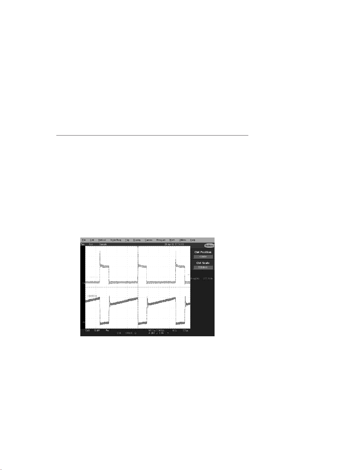
Switching Power Supply Signals: V SWITCH, I SWITCH
The V SWITCH (J2880) and I SWITCH signals are derived from the
switching power supply on the board. This power supply switches at
about 260 kHz. These signals were included to demonstrate the
current, voltage and power measurement capabilities on the
oscilloscope (see Figure 2–2).
Operating Basics
Figure 2–2: V switch, I switch
QuickStart8 DPO Demonstration Board
2–5

Operating Basics
Quadrature Amplitude Modulation Baseband Signals
QAM I, QAM Q, and QAM CLK
. These signals emulate a baseband
quadrature amplitude modulated digital signal. The clock rate of the
signal is about 1 MHz. This signal is designed to demonstrate a
number of features including FastAcq, XY and XYZ as shown in
Figures 2–3 through 2–6.
Figure 2–3: QAM I, QAM Q, and QAM CLK signals
2–6
Figure 2–4: XY display
QuickStart8 DPO Demonstration Board

Operating Basics
Figure 2–5: Y -T FastAcq display
XYZ Mode
Using the XYZ mode in place of the XY mode, permits the
instrument to sample signals at precise times when the incoming
signal is expected to be at the correct logic level. The Z parameter
comes from connecting an additional probe from Channel 3 to the
QAM CLK signal. The resulting QAM pattern will have data points
at precise locations without the noise shown in the XY QAM pattern.
Figure 2–6: XYZ FastAcq display
QuickStart8 DPO Demonstration Board
2–7

Operating Basics
A 250 mV Fast Rise Signal (Tr < 200 ps)
FAST RISE SIGNAL
. This signal (J600) has an edge that is faster than
the rise time of most oscilloscope, but T ektronix oscilloscope can
measure this signal. There is a long (relative to rise time) 50 W run
on the circuit board that is exposed and plated to allow for probing.
This is intended to demonstrate the ability of a probe and oscilloscope system to display small time differences or skew. This signal
can also be used as a deskew signal source (see Figure 2–7).
Figure 2–7: Fast Rise Signal
2–8
QuickStart8 DPO Demonstration Board

Operating Basics
Dual Random Anomalies Signals
RAND ANOM I, CHEAT I, RAND ANOM II, CHEAT II. The Random
Anomalies signals are square waves that have occasional glitches,
short pulses and other signal changes inserted at random intervals.
T wo channels are provided for demonstrating two channel anomaly
detection (see Figures 2–8 and 2–9).
Figure 2–8: Random Anomaly with cheat signal
Figure 2–9: Dual Channel Random Anomalies
QuickStart8 DPO Demonstration Board
2–9

Operating Basics
RESET ANOM
RESET ANOM. This switch (S2830) changes the signal output
frequency and amplitude in a random fashion. The number of
glitches per second is also varied by the RESET ANOM switch. The
amplitude will be a value between 2.7 and 3.2 volts and the
frequency will vary between 180 kHz and 320 kHz. The dual random
anomaly outputs can be synchronized or unsynchronized by
continuing to depress the RESET ANOM switch.
2–10
QuickStart8 DPO Demonstration Board

Operating Basics
Phase Locked VCO Output Signals
PLL VCO OUTPUT. This voltage controlled oscillator output signal
(J2410) provides a 2.5 volt (peak to peak) signal that is either
85 MHz or 68 MHz. For example, the peak-to-peak voltage is
approximately 3.1 V when oscilloscope channel has 1MW of
resistance or 1.8 V peak-to-peak when the oscilloscope channel has a
resistance of 50 W.
VCO TUNING VOLTAGE. This voltage signal drives the VCO. Phase
locked loop parameters determine how fast the VCO frequency will
change to a new programmed value.
The PLL VCO and VCO TUNING (J2520) signals are useful for
demonstrating the effect of different resolutions when comparing a
high frequency envelope of a signal to a slowly varying control
signal. This is demonstrated in Figures 2–10 and 2–11.
Figure 2–10: Low resolution display
QuickStart8 DPO Demonstration Board
2–11

Operating Basics
Figure 2–11: High resolution display
VCO MODE SELECT. This signal modifies the VCO output according
to T able 1–1 on page 1–3. Switches 3 and 4 of S2810 (a DIP switch)
allow selection of several modes of operation.
2–12
QuickStart8 DPO Demonstration Board

Operating Basics
RF Modulation
You can obtain a modulated RF signal by connecting a probe to J1
located near the SMA connector (see page 2–8). The waveform has
an amplitude that modulates between 40 and 80 mV when viewing
the individual waveforms while the frequency modulation can be
seen with a more compressed time scale.
Figure 2–12: Modulated RF display
QuickStart8 DPO Demonstration Board
2–13

Operating Basics
Pseudo Random Anomalies Signals
A five pin connector is included in the center of the board (J13) that
generates four random digital signals and a clock. These signals are
useful for demonstrating boolean trigger, state trigger, and other
kinds of triggers (see Figure 2–13).
2–14
Figure 2–13: Pseudo-Random digital signals
QuickStart8 DPO Demonstration Board

Operating Basics
Universal Serial Bus
USB DATA. USB signals from the host computer are available from J2
(see Figure 2–14). This testpoint will generate signals only when the
USB cable is used to power the board. It is also necessary to connect
a device such as a mouse to the USB output connector on the
QuickStart8 board.
Figure 2–14: USB signals
QuickStart8 DPO Demonstration Board
2–15

Operating Basics
Simulated Ground Bounce Signal An unexpected positive transition on channel 1 (J14, pin 1) is
generated whenever the signal on channel two (J14, pin 2) transitions
from positive to negative. This positive transition occurs at intervals
of 0.1 seconds to several seconds (see Figure 2–15).
2–16
Figure 2–15: Simulated Ground Bounce signal
QuickStart8 DPO Demonstration Board

Appendices

Appendix A: Diagrams
This section contains the schematic diagrams for the QuickStart8 board.
Symbols
Graphic symbols and class designation letters are based on ANSI
Standard Y32.2-1975. Abbreviations are based on ANSI Y1.1-1972.
Logic symbology is based on ANSI/IEEE Standard 91-1984 in terms of
positive logic. Logic symbols depict the logic function performed and
can differ from the manufacturer’s data.
The pound (*) after a signal name indicates that the signal performs its
intended function when in the low state.
Other standards used in the preparation of diagrams by Tektronix, Inc.,
include the following:
H Tektronix Standard 062-2476 Symbols and Practices for Schematic
Drafting
H ANSI Y14.159-1971 Interconnection Diagrams
H ANSI Y32.16-1975 Reference Designations for Electronic Equip-
ment
H MIL-HDBK-63038-1A Military Standard Technical Manual Writing
Handbook
QuickStart8 DPO Demonstration Board
A–1

Appendix A: Diagrams
Component Values
Electrical components shown on the diagrams are in the following units
unless noted otherwise:
Capacitors: Values one or greater are in picofarads (pF).
Values less than one are in microfarads (mF).
Resistors: Values are in ohms (W).
Graphic Items and Special Symbols Used in This Manual
Each assembly in the instrument is assigned an assembly number (for
example, A5). The assembly number appears in the title on the diagram
and the circuit board illustration.
Refer to
Assembly
& Diagram
Number
Offboard
Connector
A–2
Onboard
Jumper
Active Low
Signal
Digital
Ground
Internal
Screw
Adjustment
*
Signal From
Another Diagram,
Same Board
Function
Block Title
Decoupled
Voltage
Power
Termination
SYNC GENERATOR A5
Diagram
Name
Component on
back of board
Strap
Female
Coaxial
Connector
Heat Sink
Assembly
Number
QuickStart8 DPO Demonstration Board
Panel
Control
Diagram
Number

FD1
TP1
TP21
TP14
TP13
TP15
MH4
R13
TP3
MH2
C33
R11
C
C12
C160
C29
R69
C340
C25
C23C28
R50
R32
C31
C230
U5
CR3
R47
C
CR281
CR280
R12
CR4
C7R9
C10
R72
R51 C26
C24
U1
C441
R68
C320
C321
R320
R220
R230
R64
TP4
U320
R541
C
C540
C322
R420
C380
TP2
C360
R743
R741
R742
R48
R31
R28
R49
R67
Y320
TP12
C480
C5
R8
R480
T370
R10
C8
U360
R17
R15
R16
C350
C1
R27
R66
R26
R731
R74 R73
R29
R25
U530
R713
R540
R714
R30
C
DS520
C622
R520
C621
C500
C620
C510
R620
C512
C511
R510
R430
R422
C421
C420
TP10
U520
U480
U7
TP5
R36
R35
R34
R33
R733
C731
C14
R421
C
C
C19
C422
C513
C590
R62
C580
R581
CR5
C21
CR2
C27
R57
R56
C660
C13
R642
C34
R722
U610
R40
R43
R41
R44
A1 QuickStart8 board component locator
C6
U650
Q1
U550
U2
R583
R582
R650
Appendix A: Diagrams
CR1
C790
C
FD2
MH3
C32
Y970
U860
TP7
R850
C860
R24
C850
R851
C770
TP6
R19
R23
C851
R852
R22
R842
C830
U9
L2
TP16 TP19
R37
R5
R4
R2
R3
R1
TP9
FD3
MH1
U760
CR840
R65
R18
C3
C751
C840
R841
R20
C750
R744
R21
DS770
R871
R870
R762
R761
R754
R753
C11
R14
C
C870
U8
R54
R52
R53
R840
R830
U6
C30
C4
TP8
L1
R46
C22
R71 R70
C760
C762
CR650
R60
R61
R652
R58
R651
R750
R543
C530
R59
R720
R721
U4
R7
R6
C2
R38
C15
C18
C16
C20
J600
R42
R39
U3
R75
C17
R63
R76
R45
C35
TP11
QuickStart8 DPO Demonstration Board
A–3

Appendix A: Diagrams
A–4
QuickStart8 DPO Demonstration Board

Appendix A: Diagrams
QuickStart8 DPO Demonstration Board
A–5

Appendix A: Diagrams
A–6
QuickStart8 DPO Demonstration Board

Appendix A: Diagrams
QuickStart8 DPO Demonstration Board
A–7

Appendix A: Diagrams
A–8
QuickStart8 DPO Demonstration Board

Appendix A: Diagrams
QuickStart8 DPO Demonstration Board
A–9

Appendix A: Diagrams
A–10
QuickStart8 DPO Demonstration Board

Appendix A: Diagrams
QuickStart8 DPO Demonstration Board
A–11

Appendix A: Diagrams
A–12
QuickStart8 DPO Demonstration Board

Appendix A: Diagrams
QuickStart8 DPO Demonstration Board
A–13

Appendix A: Diagrams
A–14
QuickStart8 DPO Demonstration Board

Appendix A: Diagrams
QuickStart8 DPO Demonstration Board
A–15

Appendix A: Diagrams
A–16
QuickStart8 DPO Demonstration Board

Appendix A: Diagrams
QuickStart8 DPO Demonstration Board
A–17

Appendix A: Diagrams
A–18
QuickStart8 DPO Demonstration Board

Appendix A: Diagrams
QuickStart8 DPO Demonstration Board
A–19

Appendix A: Diagrams
A–20
QuickStart8 DPO Demonstration Board

Appendix B: Instrument Care
This section includes:
H Care and Maintenance
H Shipping the QuickStart8 board
Care and Maintenance
The QuickStart8 board does not require scheduled or periodic
maintenance. However, to keep good electrical contact and efficient
heat dissipation, keep the board free of dirt, dust, and contaminants.
When not in use, store the QuickStart8 board in the original shipping
bag.
Cleaning. Clean dirt and dust with a soft bristle brush. For more
extensive cleaning, use only a damp cloth moistened with deionized
water; do not use any other chemical cleaning agents.
Preventing Electrostatic Discharge. When handling the QuickStart8
board, adhere to the following precautions to avoid damaging
electronic components.
CAUTION. Static discharge can damage semiconductor components
on the QuickStart8 board.
1. Minimize handling of the board by touching only the edges.
2. Transport and store the board in the static-protected container.
3. Discharge the static voltage from your body by wearing a
grounded antistatic wrist strap while handling the training board.
4. Do not place anything capable of generating or holding a static
charge on the work station surface.
QuickStart8 DPO Demonstration Board
B–1

Appendix B: Instrucment Care
Shipping the QuickStart8 board.
T o commercially transport the QuickStart board or transformer,
package the board or transformer as follows:
1. Obtain a corrugated card board shipping carton with inside
dimensions at least six inches greater than the board or
transformer dimensions and with a carton test strength of at least
889.6 Newton Lbs/200 pounds.
2. If you are shipping the package to a T ektronix service center for
Warranty service, attach a tag to the board or transformer
showing the following:
H Owner’s name and address
H Name of a person who can be contacted
H Board or transformer type and serial number
H Description of the problem
3. Place the board in an antistatic bag to protect static-sensitive
components.
B–2
4. Tightly pack dunnage or urethane foam between the carton and
the board or transformer (allowing 7.62 cm/three inches on each
side) to cushion the board or transformer on all sides.
QuickStart8 DPO Demonstration Board

Index

Index
A
About this manual, vii
Address, Tektronix, viii
C
Care and maintenance, B–1
CHEAT I, 2–9
CHEAT II, 2–9
Component locations
power jack and USB ports, 2–4
switches, 2–4
testpoints, 2–4
Configuration
connecting the board, 1–5
VCO MODE SELECT switch,
1–3
Contacting Tektronix, viii
F
FAST RISE SIGNAL, 2–8
I
I SWITCH, 2–5
M
Manual, how to use, vii
P
Phone number, Tektronix, viii
PLL VCO output (J2410), 2–11
Power
adapter, 1–4
applying, 1–4
removing, 1–4
transformer, 1–4
USB port, 1–4
Prerequisites, 1–2
Product support, contact informa-
tion, viii
Q
Quick reference
switches, 2–3
testpoints, 2–1
USB data, 2–3
QuickStart8 board, setting up, 1–2
R
RAND ANOM I, 2–9
RAND ANOM II, 2–9
Random anomalies signals (J13),
2–14
Required materials, 1–1
BNC/SMA, 1–1
probes, 1–1
RESET ANOM (J2830), 2–10
QuickStart8 DPO Demonstration Board
Index–1

Index
S
Service support, contact informa-
tion, viii
Shipping, B–2
Signal descriptions, 2–5
250 mV fast rise (Tr < 200 ps),
2–8
phase locked VCO output, 2–11
quadrature amplitude modulation
baseband, 2–6
random anomalies signal, 2–9
simulated ground bounce signal,
2–16
switching power supply, 2–5
Signal descriptions, pseudo-random
digital, 2–14
Signals, overview, 1–6
Switches, RESET ANOM (J2830),
2–10
T
Technical support, contact informa-
tion, viii
Tektronix, contacting, viii
Testpoints
FAST RISE SIGNAL (J600), 2–8
PLL VCO output (J2410), 2–11
QAM I, QAM Q, and QAM
CLK, 2–6
quick reference, 2–1
RAND ANOM I, CHEAT I,
RAND ANOM II, CHEAT II,
2–9
random anomalies signals (J13),
2–14
simulated ground bounce signal
(J14), 2–16
USB DATA (J2), 2–15
V Switch, I Switch, 2–5
VCO MODE SELECT, 2–12
VCO TUNING VOLTAGE
(J2520), 2–11
U
URL, Tektronix, viii
USB DATA, 2–15
V
V SWITCH, 2–5
VCO MODE SELECT, 2–12
VCO TUNING VOLTAGE
(J2520), 2–11
W
Web site address, Tektronix, viii
X
XYZ mode, 2–7
Y
Y-T mode, 2–7
Index–2
QuickStart8 DPO Demonstration Board
 Loading...