


Technical Reference
TDS6000B & TDS6000C
Digital Storage Oscilloscopes
Specifications and Performance Verification
071-1659-03
Warning
The servicing instructions are for use by qualified
personnel only. To avoid personal injury, do not
perform any servicing unless you are qualified to
do so. Refer to all safety summaries prior to
performing service.
www.tektronix.com
*P071165903*
071165903

Copyright © Tektronix. All rights reserved. Licensed software products are owned by Tektronix or its subsidiaries or
suppliers, and are protected by national copyright laws and international treaty provisions.
Tektronix products are covered by U.S. and foreign patents, issued and pending. Information in this publication supercedes
that in all previously published material. Specifications and price change privileges reserved.
TEKTRONIX and TEK are registered trademarks of Tektronix, Inc.
Contacting Tektronix
Tektronix, Inc.
14200 SW Karl Braun Drive
P.O. Box 500
Beaverton, OR 97077
USA
For product information, sales, service, and technical support:
H In North America, call 1-800-833-9200.
H Worldwide, visit www.tektronix.com to find contacts in your area.

Table of Contents
Specifications 1--1.............................................
Product and Feature Description 1--1....................................
Acquisition Features 1--2..........................................
Signal Processing Features 1--2.....................................
Display Features 1--2.............................................
Measurement Features 1--3.........................................
Trigger Features 1--3..............................................
Convenience Features 1--3.........................................
Environmental and Compliance Specifications 1--4.........................
Certifications and Compliances 1--5.....................................
TDS6000B Series Specification Tables 1--7...............................
TDS6000C Series Specification Tables 1--22..............................
Performance Verification 2--1...................................
Conventions 2--2....................................................
Brief Procedures 3--1...........................................
Self Tests 3--1.......................................................
Functional Tests 3--2.................................................
Check Vertical Operation 3--3......................................
Check Horizontal Operation 3--5....................................
Check Trigger Operation 3--7.......................................
Perform the Extended Diagnostics 3--9...................................
Performance Tests 4--1.........................................
Prerequisites 4--1....................................................
Equipment Required 4--2..............................................
Test Record TDS6000B Series 4--4......................................
Test Record TDS6000C Series 4--16......................................
Signal Acquisition System Checks 4--29...................................
Check DC Voltage Measurement Accuracy 4--29........................
Check DC Gain Accuracy 4--34......................................
Check Offset Accuracy 4--50........................................
Check Maximum Input Voltage 4--54.................................
Check Analog Bandwidth 4--58......................................
Check Delay Between Channels TDS6000B Only 4--63...................
Check Channel Isolation (Crosstalk) TDS6000B Only 4--67...............
Check Input Impedance 4--72........................................
Time Base System Checks 4--73.........................................
Check Long-Term Sample Rate and Delay Time Accuracy and Reference 4--73
Check Delta Time Measurement Accuracy TDS6000B Series Only 4--76.....
Trigger System Checks 4--79............................................
Check Time Accuracy for Pulse, Glitch, Timeout, and Width Triggering 4--79.
Check Sensitivity, Edge Trigger, DC Coupled 4--82......................
Output Signal Checks 4--87.............................................
Check Outputs — CH 3 Signal Out and Aux Trigger Out 4--87.............
Fast Edge Output 4--90.............................................
Serial Trigger Checks (Option ST Only) 4--94..............................
TDS6000B & TDS6000C Series Specifications and Performance Verification
i

Table of Contents
List of Figures
Check Serial Trigger Baud Rate Limits and Word Recognizer Position
Accuracy 4--94............................................
Check Serial Trigger Clock Recovery Range 4--101.......................
Serial Trigger Checks (TDS6000C Only) 4--105.............................
Check Serial Trigger Baud Rate Limits 4--105...........................
Sine Wave Generator Leveling Procedure 4--108.............................
Figure 3--1: Universal test hookup for functional tests -- CH 1 shown 3--3
Figure 3--2: Channel button location 3--4..........................
Figure3--3:Setupfortimebasetest 3--6...........................
Figure 3--4: Setup for trigger test 3--8.............................
Figure 4--1: Initial test hookup 4--30...............................
Figure 4--2: Measurement of DC accuracy at maximum offset and
position 4--33...............................................
Figure 4--3: Initial test hookup 4--34...............................
Figure 4--4: Measurement of DC gain accuracy 4--49.................
Figure 4--5: Initial test hookup 4--51...............................
Figure 4--6: Measurement of offset accuracy 4--53....................
Figure 4--7: Initial test hookup 4--55...............................
Figure 4-- 8: Check maximum input voltage 4--57....................
Figure 4--9: Initial test hookup 4--59...............................
Figure 4--10: Measurement of analog bandwidth 4--62................
Figure 4--11: Initial test hookup 4--64..............................
Figure 4--12: Measurement of channel delay 4--66...................
Figure 4--13: Initial test hookup 4--68..............................
Figure 4--14: Initial test hookup 4--72..............................
Figure 4--15: Initial test hookup 4--73..............................
Figure 4--16: Initial test hookup 4--74..............................
Figure 4--17: Final test hookup 4--75...............................
Figure 4--18: Delta time accuracy test hookup for TDS6000B Series 4--77
Figure 4--19: Initial test hookup 4--80..............................
Figure 4--20: Measurement of time accuracy for pulse and glitch
triggering 4--81.............................................
Figure 4--21: Initial test hookup 4--83..............................
Figure 4--22: Measurement of trigger sensitivity -- 50 MHz results
shown 4--84................................................
Figure 4--23: Initial test hookup 4--88..............................
Figure 4--24: Measurement of trigger out limits 4--89.................
ii
TDS6000B & TDS6000C Series Specifications and Performance Verification

List of Tables
Table of Contents
Figure 4--25: Initial test hookup 4--90..............................
Figure 4--26: Measurement of probe compensator frequency 4--91......
Figure 4-- 27: Subsequent test hookup 4--92.........................
Figure 4--28: Measurement of probe compensator amplitude 4--93......
Figure 4--29: Initial test hookup 4--94..............................
Figure 4--30: Isolated 0 triggering 4--96............................
Figure 4--31: Isolated 1 triggering 4--98............................
Figure 4--32: N modulo 3 triggering 4--100...........................
Figure 4--33: Initial test hookup 4--101..............................
Figure 4--34: Clock recovery 4-- 104.................................
Figure 4--35: Initial test hookup 4--105..............................
Figure 4--36: Sine wave generator leveling equipment setup 4--108......
Figure 4-- 37: Equipment setup for maximum amplitude 4--110.........
Table 1--1: TDS6000B & TDS6000C Series 1--1....................
T able 1--2: Environmental specifications 1--4......................
Table 1--3: TDS6000B Series channel input and vertical
specifications 1--7..........................................
Table 1--4: TDS6000B Series horizontal and acquisition system
specifications 1--10..........................................
Table 1--5: TDS6000B Series trigger specifications 1--13..............
Table 1--6: TDS6000B Series serial trigger specifications (optional) 1--16
Table 1--7: TDS6000B Series display specifications 1--17.............
Table 1--8: TDS6000B Series input/output port specifications 1--17.....
Table 1--9: TDS6000B Series data storage specifications 1--20.........
Table 1--10: TDS6000B Series power source specifications 1--20.......
Table 1--11: TDS6000B Series mechanical specifications 1--20.........
Table 1--12: TDS6000C Series channel input and vertical
specifications 1--22..........................................
Table 1--13: TDS6000C Series horizontal and acquisition system
specifications 1--27..........................................
Table 1--14: TDS6000C Series trigger specifications 1--32.............
Table 1--15: TDS6000C Series serial trigger specifications
(Option ST) 1--35...........................................
Table 1--16: TDS6000C Series display specifications 1--37............
Table 1--17: TDS6000C Series input/output port specifications 1--37....
Table 1--18: TDS6000C Series data storage specifications 1--39........
TDS6000B & TDS6000C Series Specifications and Performance Verification
iii

Table of Contents
Table 1--19: TDS6000C Series power source specifications 1--39.......
Table 1--20: TDS6000C Series mechanical specifications 1--40.........
Table 3--1: Vertical settings 3--4.................................
Table 4--1: Test equipment 4--2..................................
Table 4--2: DC Voltage measurement accuracy, TDS6000B Series 4--31..
Table 4--3: DC Voltage measurement accuracy, TDS6000C Series 4--31..
Table 4--4: Gain accuracy, TDS6000B Series 4--36...................
Table 4--4: Gain accuracy, TDS6000C Series 4--42...................
Table 4--6: Offset accuracy, TDS6604B & TDS6804B 4--52............
Table 4--7: Offset accuracy (full scale), TDS6124C & TDS6154C 4--52..
Table 4--8: Maximum input voltage limit 4--56......................
Table 4--9: Analog bandwidth, TDS6000B 4--60.....................
Table 4--10: Analog bandwidth, TDS6000C 4--60....................
Table 4--11: Delay between channels worksheet, TDS6000B only 4--67..
Table 4--12: Delta time measurement 4--78.........................
Table 4--13: Serial pattern data 4--95..............................
T able 4--14: Word recognizer data 4--97...........................
Table 4--15: Clock recovery input frequencies and baud rates 4--103....
Table 4--16: Generator serial streams 4--106.........................
Table 4--17: Serial pattern data 4--106..............................
iv
TDS6000B & TDS6000C Series Specifications and Performance Verification

Specifications
This chapter contains the specifications for the TDS6000B & TDS6000C Series
Oscilloscopes. All specifications are guaranteed unless labeled “typical.” Typical
specifications are provided for your convenience but are not guaranteed.
Specifications that are marked with the n symbol are checked in the Perfor-
mance Tests section. To make it easier to find the specifications for a particular
product, the specifications for the TDS6000B & TDS6000C Series are listed in
separate sections.
To meet specifications, the following conditions must be met:
H The oscilloscope must have been calibrated in an ambient temperature
between 20 °C and 30 °C(68°F and 86 °F).
H The oscilloscope must be operating within the environmental limits listed in
Table 1--2, page 1--4.
H The oscilloscope must be powered from a source that meets the specifica-
tions listed in Table 1--10, page 1--20.
H The oscilloscope must have been operating continuously for at least 20
minutes within the specified operating temperature range.
H You must perform the Signal Path Compensation procedure after the
20-minute warm-up period, and the ambient temperature must not change
more than 5 °C(9°F) without first repeating the procedure. See page 3--2 for
instructions to perform this procedure.
Product and Feature Description
Your TDS6000B & TDS6000C Series is shown in Table 1--1.
Table 1- 1: TDS6000B & TDS6000C Series
Model
TDS6604B 4 6GHz 20 GS/s
TDS6804B 4 8GHz 20 GS/s
TDS6124C 4 12 GHz 40 GS/s
TDS6154C 4 15 GHz 40 GS/s
1
40 GS/s on two channels, 20 GS/s on four channels
Number of
channels
Bandwidth
Maximum sample
rate (real time)
1
1
TDS6000B & TDS6000C Series Specifications and Performance Verification
1- 1

Specifications
Acquisition Features
Separate Digitizers. Ensure accurate timing measurements with separate digitizers
for each channel. Acquisition on multiple channels is always concurrent. The
digitizers can also be combined to yield a higher sample rate on two channels
(TDS6000C series only).
Long Record Lengths. Maximum record length up to 32,000,000 points simultaneously on all four channels (TDS6000C series only; requires Option 4M)or
64,000,000 points on two channels (both TDS6000B and TDS6000C series).
Peak Detect Acquisition Mode. See pulses as narrow as 50 ps even at the slower
time base settings. Captures narrow glitches at all real-time sampling rates.
Acquisition Control. Acquire continuously or set up to capture single shot
acquisitions. Enable or disable optional acquisition features such as equivalent
time.
Horizontal Delay. Use delay when you want to acquire a signal at a significant
time interval after the trigger point. Toggle delay on and off to quickly compare
the signal at two different points in time.
Signal Processing
Features
Display Features
Average, Envelope, and Hi Res Acquisition. Use Average acquisition mode to
remove uncorrelated noise from your signal. Use Envelope to capture and
display the maximum variation of the signal. Use Hi Res to increase vertical
resolution for lower bandwidth signals.
Waveform Math. Set up simple math waveforms using the basic arithmetic
functions or create more advanced math waveforms using the math expression
editor. W aveform expressions can even contain measurement results and other
math waveforms.
Spectral Analysis. Display spectral magnitude and phase waveforms based on
your time-domain acquisitions. Control the oscilloscope using the traditional
spectrum analyzer controls such as span and center frequency.
Color LCD Display. Identify and differentiate waveforms easily with color coding.
Waveforms, readouts, and inputs are color matched to increase productivity and
reduce operating errors.
MultiView Zoom. To take advantage of the full resolution of the instrument you
can zoom in on a waveform to see the fine details. Both vertical and horizontal
zoom functions are available. Zoomed waveforms can be aligned, locked, and
automatically scrolled.
1- 2
TDS6000B & TDS6000C Series Specifications and Performance Verification

Specifications
Measurement Features
Trigger Features
Cursors. Use cursors to take simple voltage, time, and frequency measurements.
Automatic Measurements. Choose from a large palette of amplitude, time, and
histogram measurements. You can customize the measurements by changing
reference levels or by adding measurement gating.
Simple and Advanced Trigger Types. Choose simple edge trigger or choose from
eight advanced trigger types to help you capture a specific signal fault or event.
Dual Triggers. Use the A (main) trigger system alone or add the B trigger to
capture more complex events. You can use the A and B triggers together to set
up a delay-by-time or delay-by-events trigger condition.
Comm Triggers. Optional on TDS6000B & TDS6000C Series. Use comm
triggers to trigger on communication signals.
Serial Triggers. Optional on TDS6000B & TDS6000C Series. Use serial triggers
to trigger on serial pattern data.
Convenience Features
Recovered Clock and Data Triggers. Optional on TDS6000B & TDS6000C Series.
Use recovered clock and data internally to trigger your waveforms.
Autoset. Use Autoset to quickly set up the vertical, horizontal, and trigger
controls for a usable display.
Touch Screen Interface. You can operate all oscilloscope functions (except the
power switch) from the touch screen interface. If convenient, you can also install
a mouse and keyboard to use the interface.
Buttons or Menu Bar. You can choose a buttons (toolbar) operating mode,
optimized for using buttons with the touch screen, or a PC-style menu-bar
operating mode.
Open Desktop. The oscilloscope is built on a Microsoft Windows software
platform; the oscilloscope application program starts automatically when you
apply power to the instrument. You can minimize the oscilloscope application
and take full advantage of the built-in PC to run other applications. Move
waveform images and data into other applications by copying or pasting
information for short data records or exporting longer data records to a file.
TDS6000B & TDS6000C Series Specifications and Performance Verification
1- 3

Specifications
Dedicated Front Panel Controls. The front panel contains knobs and buttons to
provide immediate access to the most common oscilloscope controls. Separate
vertical controls are provided for each channel. The same functions are also
available through the screen interface.
Data Storage and I/O. The oscilloscope has a removeable hard disk drive and a
CD-RW drive, that can be used for storage and retrieval of data. The oscilloscope
has GPIB, USB, Centronics, and Ethernet ports for input and output to other
devices.
Online Help. The oscilloscope has a complete online help system that covers all
its features. The help system is context sensitive; help for the displayed control
window is automatically shown if you touch the help button. Graphical aids in
the help windows assist you in getting to the information you need. You can also
access the help topics through a table of contents or index.
Environmental and Compliance Specifications
Table 1- 2: Environmental specifications
Characteristic Description
Temperature:
Operating: TDS6000B +5 °Cto+40°C(41°F to +104 °F), excluding media
Operating: TDS6000C +10 °Cto+45°C(50°Fto+113°F)
Nonoperating -- 2 2 °Cto+60°C(8°F to +140 °F)
Humidity, Operating 20% to 80% relative humidity with a maximum wet bulb
Nonoperating 5% to 90% relative humidity with a maximum wet bulb
Altitude, Operating 3,048 m (10,000 ft)
temperature of +29 °C(+84°F) at or below +50 °C
(+122 °F), noncondensing
Upper limit derated to 25% relative humidity at +50 °C
(+122 °F)
temperature of +29 °C(+84°F) at or below +60 °C
( +140 °F), noncondensing
Upper limit derated to 20% relative humidity at +60 °C
( +140 °F)
1- 4
Nonoperating 12,190 m (40,000 ft)
Random vibration, Operating 0.27 g
3 axes, 30 minutes total, with CD-RW installed
Nonoperating 2.28 g
30 minutes total, 3 axes
from 5 Hz to 500 Hz, 10 minutes on each axis,
RMS
from 5 Hz to 500 Hz, 10 minutes on each axis,
RMS
TDS6000B & TDS6000C Series Specifications and Performance Verification

Certifications and Compliances
Specifications
EC Declaration of
Conformity - EMC
Meets intent of Directive 89/336/EEC for Electromagnetic Compatibility.
Compliance was demonstrated to the following specifications as listed in the
Official Journal of the European Communities:
EN 61326. EMC requirements for Class A electrical equipment for measurement,
control, and laboratory use. Annex D.
123
H IEC 61000--4--2. Electrostatic discharge immunity
H IEC 61000--4--3. RF electromagnetic field immunity
H IEC 61000--4--4. Electrical fast transient / burst immunity
H IEC 61000--4--5. Power line surge immunity
H IEC 61000--4--6. Conducted RF Immunity
H IEC 61000--4--11. Voltage dips and interruptions immunity
EN 61000- 3- 2. AC power line harmonic emissions
EN 61000- 3- 3. Voltage changes, fluctuations, and flicker
1
Radiated emissions may exceed the levels specified in EN 61326 when this instrument is
connected to a test object.
Australia / New Zealand
Declaration of Conformity
-EMC
2
Performance criteria for when the oscilloscope is subjected to the continuously present
electromagnetic phenomenon:
10 mV/division to 1 V/division: .0.4 division waveform displacement or .0.8 division
increase in peak- to- peak noise
Performance criteria for when the oscilloscope is subjected to transient electromagnetic
phenomenon:
Temporary, self- recoverable degradation or loss of performance is allowed, but no change
of actual operating state or loss of stored data is allowed.
3
If interconnect cables are used, they must be low- EMI shielded cables such as the
following Tektronix part numbers or their equivalents: 012- 0991- 01, 012- 0991- 02 or
012- 0991- 03 GPIB Cable; 012- 1213- 00 (or CA part number 0294- 9) RS- 232 Cable;
012- 1214- 00 Centronics Cable; or LCOM part number CTL3VGAMM- 5 VGA Cable.
Complies with EMC provision of Radiocommunications Act per these standard(s):
H AS/NZS 2064.1/2. Industrial, Scientific, and Medical Equipment: 1992
TDS6000B & TDS6000C Series Specifications and Performance Verification
1- 5

Specifications
EC Declaration of
Conformity - Low Voltage
U.S. Nationally
Recognized Testing
Laboratory Listing
Canadian Certification
Additional Compliance
Equipment Type
Safety Class
Compliance was demonstrated to the following specification as listed in the
Official Journal of the European Communities:
Low Voltage Directive 73/23/EEC, amended by 93/68/EEC.
H EN 61010-1:2001. Safety requirements for electrical equipment for
measurement control and laboratory use.
H UL 61010B--1:2004, 2nd Edition. Standard for electrical measuring and test
equipment.
H CAN/CSA C22.2 No. 61010--1--04. Safety requirements for electrical
equipment for measurement, control, and laboratory use. Part 1.
H IEC 61010--1:2001. Safety requirements for electrical equipment for
measurement, control, and laboratory use.
Test and measuring equipment.
Class 1 -- grounded product
Pollution Degree
Descriptions
Pollution Degree
A measure of the contaminates that could occur in the environment around and
within a product. Typically the internal environment inside a product is
considered to be the same as the external. Products should be used only in the
environment for which they are rated.
H Pollution Degree 1. No pollution or only dry, nonconductive pollution
occurs. Products in this category are generally encapsulated, hermetically
sealed, or located in clean rooms.
H Pollution Degree 2. Normally only dry, nonconductive pollution occurs.
Occasionally a temporary conductivity that is caused by condensation must
be expected. This location is a typical office/home environment. Temporary
condensation occurs only when the product is out of service.
H Pollution Degree 3. Conductive pollution, or dry, nonconductive pollution
that becomes conductive due to condensation. These are sheltered locations
where neither temperature nor humidity is controlled. The area is protected
from direct sunshine, rain, or direct wind.
H Pollution Degree 4. Pollution that generates persistent conductivity through
conductive dust, rain, or snow. Typical outdoor locations.
Pollution Degree 2 (as defined in IEC 61010-1). Note: Rated for indoor use only.
1- 6
TDS6000B & TDS6000C Series Specifications and Performance Verification
Specifications
Installation (Overvoltage)
Category Descriptions
Terminals on this product may have different installation (overvoltage) category
designations. The installation categories are:
H Measurement Category IV. For measurements performed at the source of
low-voltage installation.
H Measurement Category III. For measurements performed in the building
installation.
H Measurement Category II. For measurements performed on circuits directly
connected to the low-voltage installation.
H Measurement Category I. For measurements performed on circuits not
directly connected to MAINS.
Overvoltage Category
Overvoltage Category II (as defined in IEC 61010-1)
TDS6000B Series Specification Tables
The specifications for the TDS6000C Series oscilloscopes begin on page 1--22.
Table 1- 3: TDS6000B Series channel input and vertical specifications
Characteristic Description
Input channels Four
Input coupling DC 50 Ω and GND
Channel input is disconnected from input termination when
using GND coupling.
n Input impedance, DC
coupled
Maximum voltage at input <1 V
Number of digitized bits 8bits
Sensitivity range 10 mV/div to 1 V/division, in a 1-2-5 sequence
50 Ω ±2.5% at 25 _C(77_F), ±0.2% over 0 _Cto
40 _C(32_F to 104 _F)
for <100 mV settings
RMS
≤5V
for ≥100 mV settings
RMS
TDS6000B & TDS6000C Series Specifications and Performance Verification
1- 7

Specifications
Table 1- 3: TDS6000B Series channel input and vertical specifications (Cont .)
Characteristic Description
n DC gain accuracy 10 mV/div to 99.5
mV/div
±(2.5% + | 2% × (net offset/1 V) | )
100 mV/div to 1
V/div
n DC voltage measurement
accuracy
Average acquisition
mode (≥16 averages)
Delta voltage be-
tween any two aver-
ages of ≥16 wave-
forms acquired under
the same setup and
ambient conditions
Nonlinearity, typical < 1 DL, differential; ≤ 2 DL integral, independent ly based
n Analog bandwidth DC 50 Ω coupling, with amplitude tolerance of --3dB operating
Measurement type DC accuracy (in volts)
10 mV/div to
99.5 mV/div
100 mV/div to
1V/div
10 mV/div to 99.5
mV/div
100 mV/div to
1V/div
where, net offset = offset -- ( position × volts/division)
temperatures of 15 °Cto40°C(59°F to 104 °F) inclusive.
±(2.5% + | 2% × (net offset/10 V) | )
±[(2.5% + | 2% × (net offset/1 V) | ) × |
reading -- net offset | + offset accuracy
+ 0.08 division × V/division]
±[(2.5% + | 2% × (net offset/10 V) | ) ×
| reading -- net offset | + offset accuracy
+ 0.08 division × V/division]
±((2.5% + | 2% × (net offset/1 V) | )×
| reading | + 0.16 division × V/division
setting)
±((2.5% + | 2% × (net offset/10 V) | ) ×
| reading | + 0.16 division × V/division
setting)
1- 8
SCALE range Bandwidth
≥10 mV/div TDS6604B DC to ≥6GHz
TDS6804B DC to ≥7GHz
n Digitally enhanced bandwidth, DC coupled
Analog bandwidth with
P7380 or TCA-SMA adapter
for TDS6604B
Analog bandwidth with
P7380 or TCA-SMA adapter
for TDS6804B
DC 50 Ω coupling, with amplitude tolerance of --3dB operating
temperatures of 15 °Cto40°C(59°F to 104 °F).
SCALE range Bandwidth
≥10 mV/div TDS6804B DC to ≥8GHz
Full bandwidth, operating ambient 15 °Cto30°C(59°Fto
86 °F), derated by 20 MHz/ °C above 30 °C(86°F)
7 GHz, operating ambient 15 °Cto30°C(59°Fto86°F),
derated by 20 MHz/ °C above 30 °C(86°F)
TDS6000B & TDS6000C Series Specifications and Performance Verification
Specifications
Table 1- 3: TDS6000B Series channel input and vertical specifications (Cont .)
Characteristic Description
Rise time, typical No digital bandwidth enhancement
TDS6604B 10 -- 90% rise time is 70 ps vertical
sensitivities ≥ 10 mV/div
20 -- 80% rise time is 53 ps vertical
sensitivities ≥ 10 mV/div
TDS6804B 10 -- 90% rise time is 62 ps vertical
sensitivities ≥ 10 mV/div
20 -- 80% rise time is 43 ps vertical
sensitivities ≥ 10 mV/div
Digital bandwidth enhancement
TDS6804B 10 -- 90% rise time is 50 ps vertical
sensitivities ≥ 10 mV/div
20 -- 80% rise time is 35 ps vertical
sensitivities ≥ 10 mV/div
Step response settling errors,
typical
Pulse response, peak detect
or envelope mode
Position range ± 5 divisions
Offset range SCALE range Offset range
SCALE range and
step amplitude
10 mV/div to
99.5 mV/div,
with ≤ 1.5 V step
100 mV/div to
1V/div,
with ≤ 3Vstep
Sample rate setting Minimum pulse width
20 GS/s or less
10 mV/div to 50
mV/div
50.5 mV/div to
99.5 mV/div
100 mV/div to
500 mV/div
505 mV/div to
1V/div
Settling error at time after step
20 ns: ≤ 2%
1ms:≤ 0.1%
20 ns: ≤ 2%
1ms:≤ 0.2%
50 ps
±0.50 V
±0.25 V
±5V
±2.5 V
TDS6000B & TDS6000C Series Specifications and Performance Verification
1- 9
Specifications
Table 1- 3: TDS6000B Series channel input and vertical specifications (Cont .)
Characteristic Description
n Offset accuracy Volts/div setting Offset accuracy
10 mV/div to
99.5 V/div
100 mV/div to
1V/div
where, net offset = offset -- (position × volts/division)
Effective bits, typical Effective bits for 9 div peak--to--peak sine wave input sampled
at 50 mV/division and 20 GS/s.
Input frequency Effective bits
10 MHz 5.7 bits
1GHz 5.5 bits
1.5 GHz 5.4 bits
2GHz 5.2 bits
2.5 GHz 5.0 bits
3GHz 4.9 bits
4GHz 4.5 bits
5GHz 3.7 bits
6GHz 3.5 bits
6.5 GHz 3.0 bits
±(0.7% ×| net offset | + 1.5 mV + 0.1 div
× V/div setting)
±(0.8% ×| net offset | + 15 mV + 0.1 div
× V/div setting)
1- 10
7GHz 2.5 bits
n Delay between channels ≤30 ps between any two channels with the sam e scale and
coupling settings
n Channel-to-channel crosstalk
≥15:1 at rated bandwidth, and ≥80:1 at ≤1.5 GHz or the rated
bandwidth, whichever is less. Assumes two channels with the
same scale settings
Table 1- 4: TDS6000B Series horizontal and acquisition system
specifications
Characteristic Description
Real-time sample rate range Number of channels
acquired
1, 2, 3, or 4 1.25 S/s to 500 MS/s in a
Sample rate range
1-2.5-5 sequence, followed
by 1.25 GS/s, 2.5 GS/s,
5G S/s, 10 GS/s, 20 GS/s
TDS6000B & TDS6000C Series Specifications and Performance Verification

Specifications
Framelengthandmaximum
MaximumnumberofframesforSampleorPeakDetec
t
Table 1- 4: TDS6000B Series horizontal and acquisition system
specifications (Cont.)
Characteristic Description
Equivalent-time sample rate or
interpolated waveform rate range
Acquisition modes Sample, Peak Detect, Hi Res, Average, and Envelope
Record length Maximum record length supported by acquisition
Sample mode 1, 2, 3, or 4 32,000,000
10 GS/s, 12.5 GS/s, 20 GS/s, 25 GS/s, 40 GS/s,
50 GS/s, 62.5 GS/s, 80 GS/s, 100 GS/s, 125 GS/s,
160 GS/s, 200 GS/s, 250 GS/s, 312.5 GS/s, 320 GS/s,
400 GS/s, 500 GS/s, 625 GS/s, 800 GS/s, 1 TS/ s, 2 T S/s
hardware, at any sample rate
Channels Record length
Hi Res mode, ≤1.25 GS/s
sample rate
Seconds/division range 40 s/div to 25 ps/div
Maximum FastFrame update rate,
nominal
Frame length and maximum Maximum number of frames for Sample or Peak Detect
number of frames
1, 2, 3, or 4 2,000,000
310,000 frames per second
acquisition mode, depending on memory option installed
Frame length Maximum number of
frames
50 points Standard: 7008
Option 2M: 28552
Option 3M: 57280
Option 4M: 114736
250 points Standard: 4160
Option 2M: 16944
Option 3M: 33992
Option 4M: 68096
500 points Standard: 2752
Option 2M: 11232
Option 3M: 22536
Option 4M: 45152
2000 points Standard: 912
Option 2M: 3712
Option 3M: 7456
Option 4M: 14944
5000 points Standard: 384
Option 2M: 1584
Option 3M: 3184
Option 4M: 6384
n Internal time-base reference
frequency
TDS6000B & TDS6000C Series Specifications and Performance Verification
10 MHz ±2.5 ppm over any ≥100 ms interval.
Aging <1 ppm per year.
1- 11

Specifications
Table 1- 4: TDS6000B Series horizontal and acquisition system
specifications (Cont.)
Characteristic Description
n Long term sample rate and
delay time accuracy
Aperture uncertainty, typical Short term:
Time base delay time range ≤0nsto250s
±2.5 ppm over any ≥100 ms interval
≤1.5 ps RMS, records having duration ≤100 ms
≤800 fs RMS, records having duration ≤10 s
Long term:
≤15 parts-per-trillion RMS, records having duration
≤1 minute
n Delta time measurement accuracy
For a single channel, with signal amplitude >5 divisions,
reference level set at 50%, interpolation set to sin(x)/x,
volts/division set to ≥ 5 mV/div, with risetime >1.4 x T
and <4 x Tsor 150 ps (whichever is greater) and acquired
≥10 mV/Div, where T
Conditions Accuracy
Single shot signal, sample acquisition mode, Full
bandwidth
70 to 200 ps at 20 GS/s.
140 to 400 ps at 10 GS/s.
280 to 800 ps at 5 GS/s.
>100 averages, Full bandwidth selected (real or
equivalent time)
70 to 200 ps ± (4 ps + 2.5 ppm ×
is the sample period.
s
(0.06/sample rate +
2.5 ppm × | reading | ) RMS
± (0.3/sample rate +
2.5 ppm × | reading |) peak
| reading | )
s
1- 12
TDS6000B & TDS6000C Series Specifications and Performance Verification

Specifications
Table 1- 5: TDS6000B Series trigger specifications
Characteristic Description
Trigger jitter, typical 1.5 ps RMS for low frequency fast rise time signal.
n Edge Trigger Sensitivity, DC
coupled
Edge trigger sensitivity, typical All sources, for vertical scale settings ≥10 mV/div and
All sources, for vertical scale settings ≥10 mV/div and
≤1V/div
Trigger Source Sensitivity
Main trigger, Ch1 -Ch4
Delayed trigger, Ch1 -Ch4
Auxiliary input 200 mV from DC to 50 MHz,
≤1V/div
Trigger coupling Sensitivity
NOISE REJ 3x the DC-coupled limits for
AC Same as DC-coupled limits for
≤0.5 div DC to 50 MHz
≤1 div at 1.5 GHz
≤1.5 div at 3 GHz
≤2.5 div at 7 GHz (TDS6804B)
≤2.5 div at 6 GHz (TDS6604B)
≤0.5 div from DC to 50 MHz
≤1 div at 1.5 GHz
≤1.5 div at 3 GHz
≤2.5 div at 7 GHz (TDS6804B)
≤2.5 div at 6 GHz (TDS6604B)
increasing to 500 mV at 2 GHz
frequencies < 5 GHz
frequencies >100 Hz, attenuates
signals <100 Hz
HF REJ Same as DC coupled limits for
LF REJ Same as DC coupled limits for
Auxiliary trigger input resistance
and range, typical
Lowest frequency for Set Level to
50%, typical
Logic-type trigger sensitivity, typical Logic type triggers: 1.0 div, from DC to 1 GHz
50 Ω, ±5 V (DC + peak AC)
50 Hz
Runt type: 1.0 div
TDS6000B & TDS6000C Series Specifications and Performance Verification
frequencies <20 kHz, attenuates
signals >20 kHz
frequencies >200 kHz, attenuates signals <200 kHz
1- 13
Specifications
Table 1- 5: TDS6000B Series trigger specifications (Cont.)
Characteristic Description
Logic-qualified pulse-type trigger
minimum timing requirements
For vertical scale settings ≥10 mV/div and ≤1 V/div at the
TekConnect input.
Minimum logic qualifying event duration
Glitch type 100 ps 40 ps 60 ps
Runt type Runt width + 150 ps 160 ps --16 ps
Time-qualified runt type Runt width + 330 ps 160 ps 175 ps
Width type 190 ps 40 ps 175 ps
Transition type 330 ps 225 ps 175 ps
Window 190 ps --20 ps 0ps
Transition trigger, delta time
range
Events delay triggering, minimum
timing requirements, typical
Setup/Hold hold time violation
trigger, minimum clock pulse
widths, typical
1nsto1s
Minimum requirements for vertical settings from 10
mV/div to 1 V/div at the TekConnect input
Pulse width Time between channels
150 ps 1ns
For vertical settings from 10 mV/div to 1V/div at the
TekConnect input, the minimums are:
Minimum time from
active clock edge to
inactive edge
Set up time Hold time
Minimum time from inactive
clock edge to active edge
1- 14
Setup/Hold hold time violation
trigger, Setup/Hold time ranges
User’s hold time
+ 500 ps for hold
times ≥0.
User’s hold time
+ 1.5 ns for hold times
<0.
Setup time
Hold time -- 1 n s 102 ns
Setup + Hold time 500 ps
500 ps
Minimum Maximum
--100 ns 100 ns
TDS6000B & TDS6000C Series Specifications and Performance Verification
Table 1- 5: TDS6000B Series trigger specifications (Cont.)
ang
mumtimerangetowhich
ggg,p
Characteristic Description
Pulse-type trigger minimum timing
requirements
For vertical scale settings ≥10 mV/div and ≤1 V/div at the
TekConnect input
Specifications
Minimum pulse width
or transition time
Glitch type 170 ps 250 ps
Runt type 225 ps 250 ps
Time-qualified runt type 360 ps 450 ps
Width type 225 ps 250 ps
Transition type 225 ps 300 ps
n Timing accuracy for time-qualified triggers
Time range for time-qualified
triggers
The minimum to the maximum time r
the instrument can be set
for glitch trigger, pulse
trigger, or time-qualified
runt trigger.
etowhich
Time range Accuracy
360 ps to 1.5 s ± 10% of setting
1.51 sto1s ± 100 ns
500 ps to 1 s
Time range
500 ps to 950 ps 20 ps
1nsto10ns 200 ps
10.5nsto20ns 500 ps
Minimum rearm time
Time resolution
21 ns to 50 ns 1ns
52 ns to 100 ns 2ns
104 ns to 200 ns 4ns
210 ns to 500 ns 10 ns
520 ns to 2 s 20 ns
2.01 sto10ms 16 ns
10 ms to 100 ms 160 ns
100 ms to 1 s 2 s
Delayed Trigger time delay range Delay time = 5 ns to
250 s
TDS6000B & TDS6000C Series Specifications and Performance Verification
Event count = 1 to 10,000,000
1- 15
Specifications
Table 1- 5: TDS6000B Series trigger specifications (Cont.)
Characteristic Description
Trigger level or threshold range Trigger Source Sensitivity
Any channel ±12 divisions from center of
screen
Auxiliary trigger input ±5V
Line trigger ±0 V, not settable
Trigger level or threshold accuracy,
typical
Trigger position error, typical Edge trigger, DC coupling, for signals having a slew rate
Trigger holdoff range 250 ns to 12 s, maximum plus random holdoff
Edge trigger, DC coupling, for signals having rise and fall
times >1 ns
Trigger Source Accuracy
Any channel ± [(2% ×| setting -- net offset | )
+ (0.35 div × volts/div setting) +
offset accuracy]
Auxiliary Not specified
where, net offset = offset -- (position × volts/division)
at the trigger point of ≥ 0.5 division/ns
Acquisition mode Error
Sample, Average ± (1 waveform interval + 200 ps)
Peak Detect, Envelope
± (2 waveform interval + 200 ps)
Table 1- 6: TDS6000B Series serial trigger specifications (optional)
Characteristic Description
Serial trigger number of bits 64
1- 16
Serial trigger encoding types NRZ
n Serial trigger baud rate limits Up to 1.25 GBd
n Clock recovery frequency range 1.5 MBd to 3.125 GBd. Above 1250 MHz the clock is only
available internally as a trigger source. Below 1250 MHz
the clock is also available at the Recovered Clock output
along with regenerated data.
n Clock recovery jitter (RMS) <0.25% bit period + 7 ps RMS for PRBS data patterns.
<0.25% bit period + 6 ps RMS for repeating 0011 data
patterns.
TDS6000B & TDS6000C Series Specifications and Performance Verification

Specifications
Table 1- 6: TDS6000B Series serial trigger specifications (optional) (Cont.)
Characteristic Description
Clock recovery tracking/acquisition
range
± 5% of requested baud.
Minimum signal amplitude needed
for clock recovery, typical
1 division p-p up to 1.25 GBd
1.5 divisions p-p above 1.25 GBd
Table 1- 7: TDS6000B Series display specifications
Characteristic Description
Display type 210.4 mm (8.3 in) (W)× 157.8 mm (6.2 in) (H), 263 mm
(10.4 in) diagonal, liquid crystal active-matrix color display
Display resolution 1024 horizontal × 768 vertical pixels
Pixel pitch 0.2055 mm horizontal, 0.2055 mm vertical
Response time, typical 15 ms, white to black
Display refresh rate 59.94 frames per second
Viewing angle, typical Horizontal: 60 degrees left, 60 degrees right
Vertical: 45 degrees up, 60 degrees down
Displayed intensity levels Each RGB input is 6 bits, giving 64 intensity levels of
each color component
Table 1- 8: TDS6000B Series input/output port specifications
Characteristic Description
Rear-panel I/O ports Ports located on the rear panel
Video output port Upper video port, DB-15 female connector, connect a
second monitor to use dual-monitor display mode,
supports Basic requirements of PC99 specifications
Parallel port (IEEE 1284) DB-25 connector, supports the following modes:
S Standard (output only)
S Bidirectional (PS-2 compatible)
S Bidirectional enhanced parallel port (IEEE 1284
S Standard, mode 1 or mode 2, v 1.7)
S Bidirectional high-speed extended capabilities
Serial port DB-9 COM1 port, uses NS16C550-compatible UARTS,
transfer speeds up to 115.2 kb/s
Keyboard port PS-2 compatible, oscilloscope power must be off to make
connection
TDS6000B & TDS6000C Series Specifications and Performance Verification
1- 17

Specifications
Table 1- 8: TDS6000B Series input/output port specifications (Cont.)
Characteristic Description
Mouse port PS-2 compatible, oscilloscope power must be off to make
connection
LAN port RJ-45 connector, supports 10 base-T and 100 base-T and
gigabit ethernet
Audio ports Miniature phone jacks for stereo microphone input and
stereo line output
USB ports Four rear panel and one front panel USB 2.0 connectors
GPIB port IEEE 488.2 standard interface
XGA video port 15 pin D-subminiature connector on the rear panel
n DC Probe Cal Output Voltage,
Offset Voltage, and Frequency
Front-panel BNC connector for calibrating CD offset of
active probes. Signal is only present during the probe
calibration operation.
Output voltage Frequency
330 mV (from base to top)
1 kHz ± 5%
± 20% into a 50 Ω load
(Voh = 0 V, Vol = --330mV
Fast Edge Signal Output Voltage,
Offset Voltage, and Frequency
Front-panel SMA connector used as probe deskew signal
and as passive probe compensation signal
Output voltage Frequency
330 mV (from base to top)
1 kHz ± 5%
± 20% into a 50 Ω load
(Voh = 0 V, Vol = --330mV
n Auxiliary Output levels Front-panel BNC connector, provides a TTL-compatible
pulse (polarity selectable) for each A or B trigger
(selectable)
V
high V
out
≥2.5 V into open circuit,
≥1.0 V into 50 Ω load
low (true)
out
≤0.7 V with ≤4mAsink,
≤0.25 V into 50 Ω load
Auxiliary Output pulse width, typical Pulse width varies, 1 s minimum
n External Reference input
sensitivity
Vin ≥200 mV peak to peak for input frequencies between
9.8 MHz and 10.2 MHz
1- 18
External reference input frequency
range
Input voltage, maximum 7V
p-p
Input impedance 1.5 kΩ, Cin = 40 pF. Measure impedance at >100 kHz to
make the blocking capacitor invisible.
TDS6000B & TDS6000C Series Specifications and Performance Verification

Specifications
Table 1- 8: TDS6000B Series input/output port specifications (Cont.)
Characteristic Description
n External reference 9.8 MHz to 10.2 MHz. Run SPC whenever the external
reference is more than 2000 ppm different than the
internal reference or the reference at which SPC was last
run.
Input sensitivity ≥200 mV
for input frequencies between 9.8 MHz and
p-p
10.2 MHz
n Internal reference output
Frequency 10 MHz ±ኃ2.5 ppm over any ≥100 ms interval
Output voltage V
high V
out
≥2.5 V into open circuit
≥1.0 V into 50 Ω load
low (true)
out
≤0.7 V with ≤4mAsink
≤0.25 V into 50 Ω load
Serial data output baud rate range Fbd < 1250 MBd
Output swing of 1010 repeating pattern at this baud will
be at least 200 mV into 50 Ω.
Serial clock output frequency range Peak-to-peak output swing at 625 MHz is at least 200 mV
peak-to-peak into 50 Ω. Higher frequencies will be further
attenuated by approximately 6 dB per octave above
625 MHz (at 1250 MHz the amplitude will typically be
about 130 mV peak-to-peak into 50 Ω).
Either AC or DC coupled 50 Ω termination is allowed, but
with AC coupling the clock will provide 10% more
amplitude.
Serial data and clock output voltages, typical
Voh = --1.0 V, Vol = -- 1.7 V; assume load impedance
greater than 1 kΩ (50Ω source termination)
If a 50Ω or 75Ω load is used, either a DC blocking
capacitor must be put in series with the signal or the
termination must be referenced to approximately --1.3 V.
The signal amplitude will be correspondingly reduced.
Serial data output latency 15 ns (±4 ns) plus the following synchronous latency
depending on the data encoding:
35.5 clock cycles for NRZ, CMI, Manchester, and B-0-V
decoded data
36.5 clock cycles for NRZ1 decoded data
39.5 clock cycles for B3ZS decoded data
40.5 clock cycles for B4ZS decoded data
42.5 clock cycles for B6ZS decoded data
44.5 clock cycles for B8ZS decoded data
TDS6000B & TDS6000C Series Specifications and Performance Verification
1- 19
Specifications
Table 1- 9: TDS6000B Series data storage specifications
Characteristic Description
Nonvolatile memory retention time,
typical
CD-RW Front-panel CD-RW drive, read write
Hard disk Rear-panel, removeable hard disk drive (Front panel
≥5 years
location available via option FHD at time of order. Moves
CD-RW drive to rear. FHD not field retrofi table.) Capacity
will vary according to current market conditions.
Table 1- 10: TDS6000B Series power source specifications
Characteristic Description
Power consumption ≤500 Watts (650 VA)
Source voltage and frequency 100 to 240 V ±10%,50Hzto60Hz
115 V ±10%, 400 Hz
CAT II
Fuse rating Either one of the following sizes can be used, each size
requires a different fuse cap. Both fuses must be the
same type.
0.25 in x 1.25 in size UL198G and CSA C22.2, No. 59, fast acting: 8 A, 250 V
(Tektronix part number 159-0046-00, Bussman ABC-8,
Littelfuse 314008)
5 mm x 20 mm size IEC127, sheet 1, fast acting “F”, high breaking capacity:
6.3 A, 250 V (Bussman GDA 6.3, Littelfuse 21606.3)
Table 1- 11: TDS6000B Series mechanical specifications
Characteristic Description
Weight
Benchtop configuration 21 kg (47 lbs) without front cover, power cord, pouch
23 kg (50 lbs) with front cover, power cord, pouch
24 kg (53 lbs) packaged for shipment
Rackmount kit 22.4 kg (49 lbs) rackmounted instrument
5.6 kg (12.2 lbs) kit packaged for domestic shi pment
1- 20
TDS6000B & TDS6000C Series Specifications and Performance Verification

Table 1- 11: TDS6000B Series mechanical specifications (Cont.)
Characteristic Description
Dimensions
Benchtop configuration With front cover Without front cover
Specifications
278 mm (10.95 in) height,
456 mm (17.96 in) width
Rackmount configuration
(Option 1R)
Cooling Fan-forced air circulation with no air filter.
Required clearances To p 0mm(0in)
Construction material Chassis parts are constructed of aluminum alloy, front
With rack handles Without rack handles
267 mm (10.5 in) height
502 mm (19.75 in) width
642 mm (25.26 in) depth
Bottom 0 mm (0 in) when standing
Left side 76 mm (3 in)
Right side 76 mm (3 in)
Rear 0 mm (0 in) on rear feet
panel is constructed of plastic laminate, circuit boards are
constructed of glass laminate, outer shell is spray painted
finished.
277 mm (10.9 in) height,
456 mm (17.96 in) width
581 mm (22.85 in) depth
267 mm (10.5 in) height
482 mm (19 in) width
591 mm (23.26 in) depth
on feet, flip stands down
TDS6000B & TDS6000C Series Specifications and Performance Verification
1- 21
Specifications
A
ada
p
)
SMAadapter)
TDS6000C Series Specification Tables
The following tables contain the specifications for the TDS6000C Series
oscilloscopes.
NOTE. Some of the specifications use the V/FS (volts/full scale) notation. To
convert to the volts/division notation, divide the V/FS by 10.
Table 1- 12: TDS6000C Series channel input and vertical specifications
Characteristic Description
Input channels Four
Input coupling DC 50 Ω and GND
Channel input is disconnected from input termination when
using GND coupling.
n Input impedance, DC
coupled
Input VSWR, typical
(Measured with TekConnect
SM
Maximum voltage at input <1 V
Number of digitized bits 8bits
Sensitivity range 50 mV/FS to 10 V/FS (below 100 mV/FS uses zoom)
n DC gain accuracy ±2%
n DC voltage measurement
accuracy
ter
Gain setting, ≥16
averages
Delta voltage between any two averages of ≥16 waveforms acquired under
the same setup and
ambient conditions
50 Ω ± 1.5% at 25 _C(77_F),
50 Ω ±2.0% 10 _Cto45_C(50_Fto113_F)
Input frequency VSWR <1 V/FS VSWR ≥1V/FS
<2.5 GHz 1.25 1.2
<6 GHz 1.5 1.2
<14 GHz 2.1 1.5
<15 GHz 2.5 1.5
for <1 V/FS settings
RMS
5.5 V
Measurement type DC accuracy (in volts)
100 mV/FS to
10 V/FS
100 mV/FS to
10 V/FS
for ≥1 V/FS settings
RMS
±[(2% × | reading -- net offset | + offset
accuracy + 0.008 × FS]
±[(2% × | reading | + 0.016 × FS]
Where, net offset = offset -- ( position × volts/division)
Net offset is defined as the vertical value of the center of the
digitizing range, usually in volts. With Zoom off, net offset is the
center of the waveform display.
1- 22
TDS6000B & TDS6000C Series Specifications and Performance Verification
Specifications
50/
,
Enh
anc
Enh
anc
Table 1- 12: TDS6000C Series channel input and vertical specifications (Cont .)
Characteristic Description
Nonlinearity, typical < 1 DL, differential; ≤ 2 DL integral, independently based
n Analog bandwidth DC 50 Ω coupling, with amplitude tolerance of --3dB operating
temperature of 25 °C(77°F) at all gain settings when
Bandwidth Enhancement is being used.
15 GHz bandwidth is achieved with Bandwidth Enhancement
and is available at 40 GS/s only.
SCALE range Model Bandwidth
Without Bandwidth
Enhancement
With Bandwidth
Enhancement
With P7313 probe,
typical
With P7380 probe,
typical
All TDS6124C DC to >12 GHz
TDS6154C DC to >12 GHz
SCALE range Model Bandwidth
10 mV/div,
20 mV/div,
50 mV/div,
100 mV/div,
200 mV/div,
500 mV/div
Tolerance of --3dB at 15 GHz guaranteed up to 30 _C(86_F),
above 30 _C(86_F) tolerance goes down by 0.08dB per
degree C.
Without Bandwidth
Enhancement,
-- 3 d B
With Bandwidth
ement,
-- 3 d B
Without Bandwidth
Enhancement,
-- 3 d B
TDS6124C DC to >12 GHz
TDS6154C DC to >15 GHz
TDS6124C DC to 11 GHz
TDS6154C DC to 11 GHz
TDS6124C DC to 11 GHz
TDS6154C DC to 12.5 GHz
TDS6124C DC to 8 GHz
TDS6154C DC to 8 GHz
With Bandwidth
ement,
-- 3 d B
Rise time, typical Without Bandwidth Enhancement
TDS6124C 10 to 90% rise time: 30 ps
TDS6154C 10 to 90% rise time: 30 ps
TDS6000B & TDS6000C Series Specifications and Performance Verification
TDS6124C DC to 8 GHz
TDS6154C DC to 8 GHz
20 to 80% rise time: 20 ps
20 to 80% rise time: 20 ps
1- 23

Specifications
Table 1- 12: TDS6000C Series Channel input and vertical specifications
Characteristic Description
With Bandwidth Enhancement
TDS6124C 10 to 90% rise time: 31 ps
20 to 80% rise time: 22 ps
TDS6154C 10 to 90% rise time: 25 ps
20 to 80% rise time: 18 ps
Step response settling errors Gain setting full
scale
TDS6124C and TDS6154C without Bandwidth Enhancement
100 mV to 10 V/div 100≤%FS,no
TDS6124C with Bandwidth Enhancement
100 mV to 10 V/div ≤100% FS, no
TDS6154C with Bandwidth Enhancement
100 mV to 10 V/div ≤100% FS, no
Pulse response, peak detect
or envelope mode
Position range ±0.5 full scale
Sample rate setting Minimum pulse width
All
±Step amplitude Settling error at
time after step
100 ps: < 10%
more than 50% FS
overdrive
more than 50% FS
overdrive
more than 50% FS
overdrive
25 ps
400 ps: < 5%
3 ns: < 2%
1 ms: < 0.1%
100 ps: < 8%
400 ps: < 1%
3 ns: < 0.1%
1 ms: < 0.1%
100 ps: < 8%
400 ps: < 1%
3 ns: < 0.1%
1 ms: < 0.1%
1- 24
TDS6000B & TDS6000C Series Specifications and Performance Verification

Specifications
Table 1- 12: TDS6000C Series Channel input and vertical specifications (Cont .)
Characteristic Description
Offset range Gain setting Net offset range
(includes position
range)
100 mV/FS ±0.50 V ±0.45 V
200 mV/FS ±0.50 V ±0.40 V
500 mV/FS ±0.50 V ±0.25 V
1V/FS ±5V ±4.5 V
2V/FS ±5V ±4.0 V
5V/FS ±5V ±2.5 V
10 V/FS ±5V 0
Formulas for offset range calculation, excluding position
±|0.5V -- (0.5 × FS)| 100 mV/FS to 995 mV/FS
Net offset range
(excludes position
range)
±|5V -- (0.5 × FS)| 1V/FSto10V/FS
n Offset accuracy Volts/div setting Offset accuracy
100 mV/FS to
995 mV/FS
1V/FSto
10 V/FS
Net offset = offset -- (position × volts/division)
Effective bits, typical Effective bits for 0.9 × FS p--p sine wave input sampled at
500 mV/FS and 40 GS/s (Bandwidth Enhancement ON).
Input frequency Effective bits
10 MHz 5.9 bits 5.7 bits
1GHz 5.5 bits 5.3 bits
2GHz 5.4 bits 5.2 bits
3GHz 5.2 bits 5.0 bits
4GHz 5.0 bits 4.8 bits
5GHz 4.9 bits 4.7 bits
6GHz 4.8 bits 4.6 bits
7GHz 4.7 bits 4.5 bits
±(0.35% ×| net offset | + 1.5 mV +
1% × FS)
±(0.35% ×| net offset | + 15 mV +
1% × FS)
Effective bits
TDS6124C
TDS6154C
8GHz 4.6 bits 4.4 bits
9GHz 4.5 bits 4.3 bits
10 GHz 4.5 bits 4.3 bits
11 GHz 4.4 bits 4.2 bits
TDS6000B & TDS6000C Series Specifications and Performance Verification
1- 25
Specifications
c
a
Bandwidt
h
Bandwidt
h
Bandwidt
h
Table 1- 12: TDS6000C Series Channel input and vertical specifications (Cont .)
Characteristic Description
12 GHz 4.4 bits 4.2 bits
13 GHz -- 4.1 bits
14 GHz -- 4.1 bits
15 GHz -- 4.1 bits
Effective bits for 0.9 × FS p--p sine wave input sampled at
500 mV/FS and 40 GS/s (Bandwidth Enhancement OFF).
Input frequency Effective bits
TDS6124C
10 MHz 5.7 bits 5.7 bits
1GHz 5.3 bits 5.3 bits
2GHz 5.2 bits 5.2 bits
3GHz 5.0 bits 5.0 bits
4GHz 4.8 bits 4.8 bits
5GHz 4.7 bits 4.7 bits
6GHz 4.6 bits 4.6 bits
7GHz 4.5 bits 4.5 bits
8GHz 4.4 bits 4.4 bits
9GHz 4.3 bits 4.3 bits
10 GHz 4.3 bits 4.3 bits
11 GHz 4.2 bits 4.2 bits
12 GHz 4.2 bits 4.2 bits
Delay between channels ≤20 ps between any two channels with the same gain settings
Channel-to-channel crosstalk, typi
l
Conditions (GHz) TDS6124C TDS6154C
<1 V/FS, 0 to 10
150:1 150:1
Effective bits
TDS6154C
≥1 V/FS, 10 to12 80:1 80:1
<1 V/FS, 12 to15 50:1 N/A
Noise, typical
Gain setting TDS6154C
Full Scale Volts/div
100 mV 5 mV,
10 mV
160 mV 16 mV 950 V 840 V 950 V
200 mV 20 mV 1.1 mV 940 V 1mV
1- 26
TDS6000B & TDS6000C Series Specifications and Performance Verification
Enhancement ON
690 V 570 V 670 V
TDS6124C
Enhancement ON
Both with
Enhancement OFF
Specifications
g
Table 1- 12: TDS6000C Series Channel input and vertical specifications (Cont .)
Characteristic Description
300 mV 30 mV 1.6 mV 1.45 mV 1.6 mV
400 mV 40 mV 2.1 mV 1.85 mV 2.1 mV
500 mV 50 mV 2.5 mV 2.3 mV 2.4 mV
800 mV 80 mV 4.4 mV 3.8 mV 4.1 mV
900 mV 90 mV 4.8 mV 4.3 mV 4.6 mV
1 V 100 mV 6.9 mV 5.7 mV 6.8 mV
2 V 200 mV 10.5 mV 9.5 mV 10 mV
5 V 500 mV 25 mV 23 mV 24 mV
10 V 1 V 56 mV 46 mV 50 mV
Table 1- 13: TDS6000C Series horizontal and acquisition system
specifications
Characteristic Description
Real-time sample rate range 1.25 S/s to 500 MS/s in a 1-2.5-5 sequence followed by
1.25 GS/s, 2.5 GS/s, 5 GS/s,10 GS/s, 20 GS/s, 40 GS/s with
either on channel turned on or the following t wo-channel
combinations: Ch1/Ch3, Ch1/Ch4, Ch2/Ch3, Ch2/Ch4. Other
two-channel combinations or more than two channels only go t o
20 GS/s.
Equivalent-time sample rate
or interpolated waveform
rate range
Acquisition modes Sample, Peak Detect, Hi Res, Average, Envelope, and
10 GS/s, 12.5 GS/s, 20 GS/s, 25 GS/s, 40 GS/s,
50 GS/s, 62.5 GS/s, 80 GS/s, 100 GS/s, 125 GS/s,
160 GS/s, 200 GS/s, 250 GS/s, 312.5 GS/s, 320 GS/s,
400 GS/s, 500 GS/s, 625 GS/s, 800 GS/s, 1 TS/ s, 2 T S/s
Waveform Database
TDS6000B & TDS6000C Series Specifications and Performance Verification
1- 27
Specifications
Framelengthandmaximum
MaximumnumberofframesforSampleorPeakDetec
t
Table 1- 13: TDS6000C Series horizontal and acquisition system
specifications (Cont.)
Characteristic Description
Record length Maximum record length supported by acquisition hardware:
Channels Record length
Sample mode
operating at
10 GS/s, 20 GS/s,
40 GS/s
Sample mode
operating at
≤5 GS/s
Sample mode
operating at
10 GS/s, 20 GS/s
Sample mode
operating at
≤5 GS/s
High Resolution
mode operating at
≤1.25 GS/s
Seconds/division range 40 s/div to 25 ps/div
Maximum FastFrame update
rate, nominal
Frame length and maximum Maximum number of frames for Sample or Peak Detect
number of frames
1or2
1or2 32 M
3or4 32 M
3or4 16 M
1, 2, 3, or 4 2M
310,000 frames per second
acquisition mode, depending on memory option installed
Frame length Maximum number of frames
64 M
50 points Option 4M: 114736
250 points Option 4M: 68096
500 points Option 4M: 45152
2000 points Option 4M: 14944
5000 points Option 4M: 6384
n Long term timebase and
delay time accuracy
Aperture uncertainty, typical Tot al:
1- 28
TDS6000B & TDS6000C Series Specifications and Performance Verification
±2 ppm initial accuracy. Aging <1 ppm per year from the date of
factory calibration.
<350 fs RMS, for record duration <10 s
<2.5 ps peak, for record duration <10 s
<2 ps + 15 parts/trillion, for record duration >20 s
Random Jitter only (excludes interleaving errors)
<300 fs RMS, for record duration <10 s
<2.5 ps peak, for record duration <10 s
<2 ps + 15 parts/trillion, for record duration >20 s

Table 1- 13: TDS6000C Series horizontal and acquisition system
specifications (Cont.)
Characteristic Description
Aperture uncertainty (long
tem), typical
Time base delay time range 5nsto250s
≤15 parts per trillion RMS, records having duration ≤1 minute
Specifications
Delta time measurement
accuracy, typical
Approximate formula to calculate delta-time measurement
accuracy (DTA) for a given instrument setting and input signal is
shown below (assumes insignificant signal content above
Nyquist):
A = input signal amplitude (volts)
t
= 10 to 90% measured rise time (seconds)
rm
N = input-referred noise ( volts RMS)
t
= short/medium term aperture uncertainty (seconds RMS)
j
TBA = time base accuracy (2 ppm)
duration = delta-time measurement (seconds)
assume edge shape that results from Guassian filter response.
2
N
DTA
Assumes insignificant error due to aliasing.
For time durations less than 100 ns, the rms ji tter i n DTA
measurements can be estimated as:
DTA
= 5 × 2 × Ꮑ
pk−pk
= 2 × Ꮑ
Ꭹ
rms
Ꭹ
Ꮑ
× t
rm
A
TBA × duration (seconds peak--to--peak)
× t
2
Ꮖ
+ t
rm
N
Ꮑ
A
2
Ꮖ
+ t
j
2
Ꮖ
(seconds rms)
j
Ꮖ
+
The term under the square-root sign is the stability, and is due to
TIE. The errors due to this term occur throughout a single-shot
measurement. The second term is due to both the absol ute
center-frequency accuracy and the center-frequency stability of
the timebase and varies between multiple single-shot
measurements over the observation interval (the amount of time
from the first single-shot measurement to the final single-shot
measurement). The observation interval may not exceed 1 year.
TDS6000B & TDS6000C Series Specifications and Performance Verification
1- 29
Specifications
Table 1- 13: TDS6000C Series horizontal and acquisition system
specifications (Cont.)
Characteristic Description
TDS6154C Bandwidth Enhancement ON, single shot, sample mode,
assume full-scale setting of 500 mV and signal amplitude of
350 mV
10--90%
Risetime (trm)
25 ps <100 ns 556 fs 2.98 ps
35 ps <100 ns 608 fs 3.24 ps
40 ps <100 ns 639 fs 3.39 ps
60 ps <100 ns 783 fs 4.11 ps
80 ps <100 ns 948 fs 4.94 ps
100 ps <100 ns 1.12 ps 5.82 ps
TDS6124C Bandwidth Enhancement ON, single shot, sample mode,
assume full--scale setting of 500 mV and signal amplitude of
350 mV
Duration DTA rms DTA pkpk
10--90%
Risetime (trm)
35 ps <100 ns 570 fs 3.05 ps
40 ps <100 ns 591 fs 3.16 ps
60 ps <100 ns 693 fs 3.66 ps
80 ps <100 ns 814 fs 4.27 ps
100 ps <100 ns 948 fs 4.94 ps
Duration DTA rms DTA pkpk
1- 30
TDS6000B & TDS6000C Series Specifications and Performance Verification
Table 1- 13: TDS6000C Series horizontal and acquisition system
specifications (Cont.)
Characteristic Description
Jitter noise floor, typical TDS6124C TDS6154C
420 fs 420 fs
Applies to time periods as long as 10 s
The formula to calculate jitter noise floor (JNF) for a given
instrument setting is given below:
FS = Full scale setting (volts)
A = signal amplitude as a fraction of full scale
trm = 10 to 90% displayed (or measured) rise time (seconds)
N = Input-referred noise (volts RMS)
= short term aperture uncertainty (seconds RMS)
tj
2
JNF =
Ꭹ
Ꮑ
FS × A
N
× trm
2
Ꮖ
+ t
(seconds rms)
j
Specifications
Numbers used for the above calculations:
TDS6124C: FS = 500 mv, A = 0.8, trm = 42 ps,
N=2.1mV,t
TDS6154C: FS = 500 mv, A = 0.8, trm = 30 ps,
N=2.6mV,t
= 350 fs
j
= 350 fs
j
TDS6000B & TDS6000C Series Specifications and Performance Verification
1- 31

Specifications
c
c
a
c
a
Table 1- 14: TDS6000C Series trigger specifications
Characteristic Description
Trigger jitter, typical 1 ps RMS for low frequency fast rise time signal.
Edge Trigger Sensitivity DC
oupled, typi
Edge trigger sensitivity,
typical
l
All sources, for vertical scale settings ≥10 mV/div and ≤1V/div.
Trigger Source
Main trigger, Ch1 thru
Ch4
Delayed trigger, Ch1 thru
Ch4
Auxiliary trigger 250 mV from DC to 50 MHz, increas-
All sources, for all vertical scale settings.
Trigger coupling Sensitivity
NOISE REJ 15%xFSfromDCto50MHz
AC Same as DC-coupled limits for
HF REJ Same as DC coupled limits for
Sensitivity
4%xFSfromDCto50MHz
10% x FS at 3 GHz
30% x FS at 9 GHz
4%xFSfromDCto50MHz
10% x FS at 3 GHz
30% x FS at 9 GHz
ing to 500 mV at 2 GHz
35% x FS at 3 GHz
50% x FS at 5 GHz
frequencies >100 Hz, attenuates
signals <100 Hz
frequencies <20 kHz, attenuates
signals >20 kHz
1- 32
LF REJ Same as DC coupled limits for
frequencies >200 kHz, attenuates
signals <200 kHz
Auxiliary trigger input resistance and range, typical
Auxiliary trigger level range ±4.5 V
Lowest frequency for Set
Level to 50%, typical
Events delay triggering,
minimum timing requirements, typi
Delayed trigger event counter range
n Delayed trigger time
delay range
l
50 Ω, ±5 V (DC + peak AC)
50 Hz
Minimum requirements for vertical settings from 10 mV/div to
1 V/div at the TekConnect input
Pulse width
100 ps 1.1 ns
1 to 10,000,000
3.2nsto3Ms
Time between channels
TDS6000B & TDS6000C Series Specifications and Performance Verification

Table 1- 14: TDS6000C Series trigger specifications (Cont.)
Characteristic Description
Trigger sensitivity, typical Specified at the TekConnect input:
Logic type triggers: 1.5 div, from DC to 1 GHz
(for 10 mV/div to 1 V/div vertical settings)
Runt type: 1.5 div
Width and glitch 1.5 div, from DC to 1 GHz
Specifications
n Minimum timing requirements
Width trigger 120 ps, 620 ps n/a n/a
Logic qualified width
trigger
Glitch trigger 70 ps, 215 ps n/a n/a
Logic qualified glitch
trigger
Runt trigger 130 ps, 280 ps n/a n/a
Time qualified runt
trigger
Logic qualified runt
trigger
Time and logic
qualified runt trigger
Window trigger 320 ps, 460 ps n/a n/a
Logic qualified
Window trigger
For vertical scale settings ≥10 mV/div and ≤1 V/div at the
TekConnect input.
Minimum pulse width,
Minimum rearm time
190 ps, 250 ps 40 ps 175 ps
100 ps, 250 ps 112 p s 36 ps
476 ps, 510 ps n/a n/a
210 ps, 250 ps 408 ps 105 ps
520 ps, 360 ps 160 ps 105 ps
190 ps, 460 ps 260 ps 105 ps
Setup time Hold time
Transition trigger 490 ps, 670 ps n/a n/a
Logic qualified transition trigger
Timeout trigger 550 ps, 300 ps +
Logic qualified Timeout trigger
420 ps, 670 ps 220 ps 92 ps
Maxim ignored pulse
width, Minimum rearm
time
pulse width
620 ps, 300 ps +
pulse width
TDS6000B & TDS6000C Series Specifications and Performance Verification
Setup time Hold time
n/a n/a
92 ps 0ps
1- 33
Specifications
c
a
g
ger,ty
pic
a
trigger,typical
c
a
300psonlyappliestotriggertypesthatcansupportapulsethi
s
Table 1- 14: TDS6000C Series trigger specifications (Cont.)
Characteristic Description
Minimum timing requirements, logi
tri
nd state type
l
Minimum duration of logic state: 100 ps (10 Gbps)
Trigger type Min pulse width Rearm time
Logic 80 ps 660 ps
State 168 ps 580 ps
Time qualified logic 130 ps 630 ps
Transition trigger, delta time
range
Setup/Hold violation trigger,
setupand hold ranges
Setup/Hold hold time violation trigger, minimum clock
pulse widths, typi
n Timing accuracy for
time-qualified triggers
l
1nsto1s
Feature Minimum Maximum
Setup time
Hold time -- 1 n s 102 ns
Setup + Hold time 500 ps
For vertical settings from 10 mV/div to 1V/div at the TekConnect
input, the minimums are:
Minimum time from active clock edge to inactive edge
User’s hold time +500 ps
for hold times ≥0.
User’s hold time +1.6 ns
for hold times <0.
Typical, for range of 1 ns to 1.8 ns.
Time range Accuracy
<500 ns ± (20% of setting + 0.5 ns)
520 ns to 1 s ± (0.01% of setting + 100 ns)
--100 ns 100 ns
Minimum time from inactive clock
edge to active edge
500 ps
Time range for time-qualified
triggers
Minimum to maximum time range to
which the instrument
canbesetforglitch
trigger, pulse trigger,
or time-qualified runt
trigger.
1- 34
TDS6000B & TDS6000C Series Specifications and Performance Verification
300 ps to 1 s
narrow. For example, time-qualified runt can only recognize
pulses down to 500 ps.

Table 1- 14: TDS6000C Series trigger specifications (Cont.)
Characteristic Description
Trigger level or threshold Trigger Source Sensitivity
range
Any channel
Auxiliary trigger input ±5V
Line trigger ±0 V, not settable
±0.6 × FS from center of screen
Specifications
Trigger level or threshold
accuracy, typical
Trigger position error, typical Edge trigger, DC coupl ing, for signal s having a slew rate at the
Trigger holdoff range 250 ns to 12 s plus random holdoff
Edge trigger, DC coupling, for signals having rise and fall times
>1 ns
Trigger Source Accuracy
Any channel ± [(2% ×| trigger level -- net offset | )
+ (3.5% × FS) + offset accuracy]
Auxiliary Not specified
where, net offset = offset -- (position × volts/division)
trigger point of ≥ 5% FS/ns
Acquisition mode Error
Sample, Average ± (1 waveform interval + 50 ps)
Peak Detect, Envelope ± (2 waveform interval + 50 ps)
Table 1- 15: TDS6000C Series serial trigger specifications (Option ST)
Characteristic Description
Serial trigger number of bits 64, ≤1.25 Gbd
40, >1.25 Gbd
Serial trigger, serial
decoding
nSerial trigger baud rate
limits
nClock recovery frequency
range
NRZ, ≤1.25 Gbd
8B10B, 1.25 Gbd to 3.125 GBd
Up to 3.125 Gbd
>1.25 Gbd requires 8B10B encoded data
1.5 MBd to 3.125 GBd. Above 1250 MHz t he clock is only
available internally as a trigger source. Below 1250 MHz t he
clock is also available at the Recovered Clock output along with
regenerated data.
TDS6000B & TDS6000C Series Specifications and Performance Verification
1- 35

Specifications
accuracy
Table 1- 15: TDS6000C Series serial trigger specifications (Option ST) (Cont.)
Characteristic Description
Clock recovery jitter (RMS),
typical
<0.25% bit period + 2 ps RMS for PRBS data patterns.
<0.25% bit period + 1.5 ps RMS for repeati ng 0011 data patterns.
Bit rate Pattern Jitter (RMS)
3.125 Gbd 00110011 2.8 ps
2.74 Gbd 00110011 2.9 ps
2.35 Gbd 00110011 3.1 ps
2.34 Gbd 00110011 3.1 ps
1.95 Gbd 00110011 3.3 ps
1.57 Gbd 00110011 3.6 ps
100 MBd 00110011 27 ps
10 MBd 00110011 252 ps
n Serial trigger, serial
word recognizer position
Clock recovery tracking/acquisition range
Minimum signal amplitude
needed for clock recovery,
typical
Edge trigger, DC coupling, for signals having a slew rate at the
trigger point of ≥ 5% FS/ns
Acquisition mode Error
Sample, Average ± (1 waveform interval + 50 ps)
Peak Detect, Envelope ± (2 waveform interval + 50 ps)
± 5% of requested baud.
1 division p-p up to 1.25 GBd
1.5 divisions p-p above 1.25 GBd
1- 36
TDS6000B & TDS6000C Series Specifications and Performance Verification

Specifications
Table 1- 16: TDS6000C Series display specifications
Characteristic Description
Display type 210.4 mm (8.3 in) (W)× 157.8 mm (6.2 in) (H), 263 mm (10.4 in)
diagonal, liquid crystal active-matrix color display
Display resolution 1024 horizontal × 768 vertical pixels
Pixel pitch 0.2055 mm horizontal, 0.2055 mm vertical
Response time, typical 15 ms, white to black
Display refresh rate 59.94 frames per second
Viewing angle, typical Horizontal: 60 degrees left, 60 degrees right
Vertical: 45 degrees up, 60 degrees down
Displayed intensity levels Each R-G-B input is 6 bits, giving 64 intensity levels of each color
component
Table 1- 17: TDS6000C Series input/output port specifications
Characteristic Description
Rear-panel I/O ports Ports located on the rear panel
Video output port Upper video port, DB-15 female connector, connect a
second monitor to use dual-monitor display mode,
supports Basic requirements of PC99 specifications
Parallel port (IEEE 1284) DB-25 connector, supports the following modes:
-standard (output only)
bidirectional (PS-2 compatible)
bidirectional enhanced parallel port (IEEE 1284
standard, mode 1 or mode 2, v 1.7)
-bidirectional high-speed extended capabilities
Serial port DB-9 COM1 port, uses NS16C550-compatible UARTS,
transfer speeds up to 115.2 kb/s
Keyboard port PS-2 compatible, power must be off to make connection
Mouse port PS-2 compatible, power must be off to make connection
LAN port RJ-45 connector, supports 10 base-T and 100 base-T and
gigabit ethernet
Audio ports Miniature phone jacks for stereo microphone input and
stereo line output
USB ports Two rear panel USB 2.0 connectors
GPIB port IEEE 488.2 standard interface
XGA video port 15 pin D-subminiature connector on the rear panel
TDS6000B & TDS6000C Series Specifications and Performance Verification
1- 37

Specifications
Table 1- 17: TDS6000C Series input/output port specifications (Cont.)
Characteristic Description
n DC Probe Cal Output Voltage,
Offset Voltage, and Frequency
Front-panel BNC connector for calibrating CD offset of
active probes. Signal is only present during the probe
calibration operation.
Output voltage Frequency
810 mV (from base to top)
1 kHz ± 5%
± 20% into a > 10 kΩ load
(Voh = 0.56 V, Vol =
--0.25 V typical)
440 mV ± 20% into a 50 Ω
load (Voh = 0.30 V, Vol =
--0.14 V typical)
Fast Edge Signal Output Voltage,
Offset Voltage, and Frequency
Front-panel SMA connector used as probe deskew signal
and as passive probe compensation signal
Output voltage Frequency
330 mV (from base to top)
1 kHz ± 5%
± 20% into a 50 Ω load
(Voh = 0 V, Vol = 330mV)
n Auxiliary Output levels Front-panel BNC connector, provides a TTL-compatible
pulse (polarity selectable) for each A or B trigger
(selectable)
V
nExternal Reference input
sensitivity
high V
out
≥2.5 V into open circuit
≥1.0 V into 50 Ω load
Vin ≥200 mV peak-to-peak for input frequencies between
9.8 MHz and 10.2 MHz
low (true)
out
≤0.7 V with ≤4mAsink
≤0.25 V into 50 Ω load
1- 38
n External reference input
frequency range
9.8 MHz to 10.2 MHz. Run SPC whenever the external
reference is more than 2000 ppm different than the
internal reference or the reference when SPC was last
run.
External reference input voltage,
7V
p-p
maximum
External reference input impedance 1.5 kΩ, Cin = 40 pF. Measure impedance at >100 kHz to
make the blocking capacitor invisible.
External reference Input sensitivity ≥200 mV
for input frequencies between 9.8 MHz and
p-p
10.2 MHz
TDS6000B & TDS6000C Series Specifications and Performance Verification

Specifications
Table 1- 17: TDS6000C Series input/output port specifications (Cont.)
Characteristic Description
n Internal reference output Output is enabled when user selects Internal Reference
from the user interface
Frequency 10 MHz over any ≥100 ms interval
Output voltage V
Serial data output baud rate range Fbd < 1250 MBd
Serial clock output frequency range Peak-to-peak output swing at 625 MHz is at least 200 mV
high V
out
≥2.5 V into open circuit
≥1.0 V into 50 Ω load
Output swing of 1010 repeating pattern at this baud will
be at least 200 mV into 50 Ω.
peak-to-peak into 50 Ω. Higher frequencies will be further
attenuated by approximately 6 dB per octave above
625 MHz (at 1250 MHz the amplitude will typically be
about 130 mV peak-to-peak into 50 Ω).
Either AC or DC coupled 50 Ω termination is allowed, but
with AC coupling the clock will provide 10% more
amplitude.
low (true)
out
≤0.7 V with ≤4mAsink
≤0.25 V into 50 Ω load
Table 1- 18: TDS6000C Series data storage specifications
Characteristic Description
Nonvolatile memory retention time,
typical
N.A., data is stored on the hard disk drive
CD-RW Front-panel CD-RW drive
Hard disk Rear-panel, removeable hard disk drive (Front panel
location available via option FHD at time of order. Moves
CD-RW drive to rear. FHD not field retrofi table.) Capacity
will vary according to current market conditions.
Table 1- 19: TDS6000C Series power source specifications
Characteristic Description
Power consumption ≤500 Watts (650 VA)
Source voltage and frequency 100 to 240 V ±10%,50Hzto60Hz
115 V ±10%, 400 Hz
CAT II
TDS6000B & TDS6000C Series Specifications and Performance Verification
1- 39

Specifications
Table 1- 19: TDS6000C Series power source specifications (Cont.)
Characteristic Description
Fuse rating size Either one of the following sizes can be used; each size
requires a different fuse cap. Both fuses must be the
same type
0.25 in × 1.25 in UL198G and CSA C22.2, No. 59, fast acting: 8 A, 250 V
(Tektronix part number 159-0046-00, Bussman ABC-8,
Littelfuse 314008)
5mm× 20 mm IEC127, sheet 1, fast acting “F”, high breaking capacity:
6.3 A, 250 V (Bussman GDA 6.3, Littelfuse 21606.3)
Table 1- 20: TDS6000C Series mechanical specifications
Characteristic Description
Weight
Benchtop configuration 21 kg (47 lbs) without front cover, power cord, pouch
23 kg (50 lbs) with front cover, power cord, pouch
24 kg (53 lbs) packaged for shipment
Rackmount kit 22.4 kg (49 lbs) rackmounted instrument
5.6 kg (12.2 lbs) kit packaged for domestic shi pment
Dimensions
Benchtop configuration With front cover Without front cover
278 mm (10.95 in) height
456 mm (17.96 in) width
Rackmount configuration
(Option 1R)
Cooling Fan-forced air circulation with no air filter.
Required clearances Top 0mm(0in)
With rack handles Without rack handles
267 mm (10.5 in) height
502 mm (19.75 in) width
642 mm (25.26 in) depth
Bottom 0 mm (0 in) when standing
Left side 76 mm (3 in)
Right side 76 mm (3 in)
277 mm (10.9 in) height
456 mm (17.96 in) width
581 mm (22.85 in) depth
267 mm (10.5 in) height
482 mm (19 in) width
591 mm (23.26 in) depth
on feet, flip stands down
1- 40
Rear 0 mm (0 in) on rear feet
Construction material Chassis parts are constructed of aluminum alloy, front
panel is constructed of plastic laminate, circuit boards are
constructed of glass laminate, outer shell is spray painted
finished.
TDS6000B & TDS6000C Series Specifications and Performance Verification

Performance Verification
Two types of Performance Verification procedures can be performed on this
product: Brief Pr ocedures and Performance Tests. You may not need to perform
all of these procedures, depending on what you want to accomplish.
H To rapidly confirm that the oscilloscope functions and was adjusted properly,
just do the brief procedures under Self Tests, which begin on page 3--1.
Advantages: These procedures are quick to do, require no external
equipment or signal sources, and perform extensive functional and accuracy
testing to provide high confidence that the oscilloscope will perform
properly. They can be used as a quick check before making a series of
important measurements.
H To further check functionality, first do the Self Tests just mentioned; then do
the brief procedures under Functional Tests that begin on page 3--2.
Advantages: These procedures require minimal additional time to perform,
require no additional equipment other than a BNC cable and BNC-to-SMA
adapter or a TCA-SMA adapter, and these procedures more completely test
the internal hardware of the oscilloscope. They can be used to quickly
determine if the oscilloscope is suitable for putting into service, such as
when it is first received.
H If more extensive confirmation of performance is desired, do the Perform-
ance Tests, beginning on page 4--1, after doing the Functional and Self Tests
mentioned above.
Advantages: These procedures add direct checking of the warranted
specifications that are marked with the n symbol. These procedures require
specific test equipment. (See Table 4--1: Test equipment on page 4--2).
If you are not familiar with operating the oscilloscope, read the oscilloscope
reference or user manuals or explore the online help.
TDS6000B & TDS6000C Series Specifications and Performance Verification
2- 1

Performance Verification
Conventions
Throughout these procedures the following conventions apply:
H Each test procedure uses the following general format:
Title of Test
Equipment Required
Prerequisites
Procedure
H Each procedure consists of as many steps, substeps, and subparts as required
to do the test. Steps, substeps, and subparts are sequenced as follows:
1. First Step
a. First Substep
H First Subpart
H Second Subpart
b. Second Substep
2. Second Step
H In steps and substeps, the lead-in statement in italics instructs you what to
do, while the instructions that follow tell you how to do it, as in the example
step below:
Initialize the oscilloscope: Push the front-panel DEFAULT SETUP button.
H Where instructed to use a control in the display or a front-panel button or
knob, the name of the control, button, or knob appears in boldface type.
Where instructed to make or verify a setting, the value of the setting also
appears in boldface type.
STOP.TheSTOP notation at the left is accompanied by information you must
read to do the procedure properly.
H The term “toolbar” refers to a row of buttons at the top of the display. The
term “menu bar” refers to a row of menus at the top of the display. You can
switch between toolbar and menu bar operating modes by touching the
button near the top right corner of the display.
2- 2
H The procedures assume you have connected a mouse to the oscilloscope so
that you can click on the screen controls. If you have not connected a mouse,
you can use the touch screen to operate all the screen controls.
TDS6000B & TDS6000C Series Specifications and Performance Verification

Performance Verification
H Some of the specifications for the TDS6000C Series oscilloscopes use the
V/FS (volts/full scale) notation. To convert to the volts/division notation,
divide the V/FS by 10.
H Some of the early TDS6000B Series oscilloscopes have the Fast Edge SMA
connector labeled “Probe Compensation” and the DC Probe Cal BNC
connector labeled “Probe Cal.” These connectors have the same functions
and signals as both label sets. All of the illustrations in this document use the
Fast Edge label and DC Probe Cal label. If your instrument has the earlier
labels, follow the steps described with the new labels.
TDS6000B & TDS6000C Series Specifications and Performance Verification
2- 3

Performance Verification
2- 4
TDS6000B & TDS6000C Series Specifications and Performance Verification

Brief Procedures
Self Tests
The Self Tests use internal routines to confirm basic functionality and proper
adjustment. No test equipment is required to do these test procedures.
The Functional Tests utilize the FAST EDGE output at the front panel as a
test-signal source for further verifying that the oscilloscope functions properly. A
SMA cable and a TCA-SMA adapter are required to do these test procedures.
This procedure uses internal routines to verify that the oscilloscope functions and
was adjusted properly. No test equipment or hookups are required.
Equipment
required
Prerequisites Power on the oscilloscope and allow a 20 minute warm-up before doing
1. Verify that internal diagnostics pass: Do the following substeps to verify
passing of internal diagnostics.
a. Display the System diagnostics menu:
H If the oscilloscope is in toolbar mode, click the MENU button to put
the oscilloscope into menu bar mode.
H Select Instrument Diagnostics from the Utilities menu and. This
displays the diagnostics control window.
b. Run the System Diagnostics:
H First disconnect any input signals from all four channels.
H Click the Run button in the diagnostics control window.
c. Wait: The internal diagnostics do an exhaustive verification of proper
oscilloscope function. This verification may take several minutes. When
the verification is finished, the resulting status will appear in the
diagnostics control window.
None
this procedure.
TDS6000B & TDS6000C Series Specifications and Performance Verification
3- 1

Brief Procedures
NOTE. If diagnostic error message 512 is displayed, run signal-path compensation then re-run diagnostic.
d. Verify that no failures are found and reported on-screen. All tests should
pass.
e. Run the signal-path compensation routine:
H Select Instrument Calibration from the Utilities menu .... This
displays the instrument calibration control window.
H If required because the instrument is in service mode, select the
Signal Path button under Calibration Area.
NOTE. Signal Path Compensation is not valid until the instrument reaches a
valid temperature. Calibration Status must be Te m p.
H Click the Calibrate button to start the routine.
Functional Tests
f. Wait: Signal-path compensation may take five to fifteen minutes to run.
g. Confirm signal-path compensation returns passed status: Verify that the
word Pass appears in the instrument calibration control window.
2. Return to regular service: Click the Close button to exit the instrument
calibration control window.
The purpose of these procedures is to confirm that the instrument functions
properly.
NOTE. These procedures verify that the instrument features operate. They do not
verify that they operate within limits.
Therefore, when the instructions in the functional tests that follow call for you to
verify that a signal appears on-screen “that is about five divisions in amplitude”
or “has a period of about six horizontal divisions,” and so forth, do not
interpret the quantities given as limits.
3- 2
TDS6000B & TDS6000C Series Specifications and Performance Verification

Brief Procedures
NOTE. Do not make changes to the front-panel settings that are not called out in
the procedures. Each verification procedure will require you to set the instrument
to certain default settings before verifying functions. If you make changes to
these settings, other than those called out in the procedure, you may obtain
invalid results. In this case, repeat the procedure from step 1.
When you are instructed to press a front-panel button or screen button, the
button may already be selected (its label w ill be highlighted). If this is the case,
it is not necessary to push the button.
Check Vertical Operation
Equipment
required
Prerequisites None
One SMA cable, such as Tektronix part number 174-1427-xx
One TCA-SMA adapter
TDS6000B or TDS6000C Digital Storage Oscilloscope
1. Initialize the instrument: Push the front-panel DEFAULT SETUP button.
2. Hook up the signal source: Connect the equipment as shown in Figure 3--1
to the channel input you want to test (beginning with CH 1).
NOTE. Connect the FAST EDGE output (labeled PROBE COMPENSATION on
some TDS6000B instruments) to the channel input using a SMA cable and
adapters.
3. Turn off all channels: If any of the front-panel channel buttons are lighted,
push those buttons to turn off the displayed channels. See Figure 3--2.
4. Select the channel to test: Push the channel button for the channel you are
currently testing. The button lights and the channel display comes on.
Instrument under test
SMA cable from FAST
EDGE output to CH 1
input
Figure 3- 1: Universal test hookup for functional tests - CH 1 shown
TDS6000B & TDS6000C Series Specifications and Performance Verification
3- 3
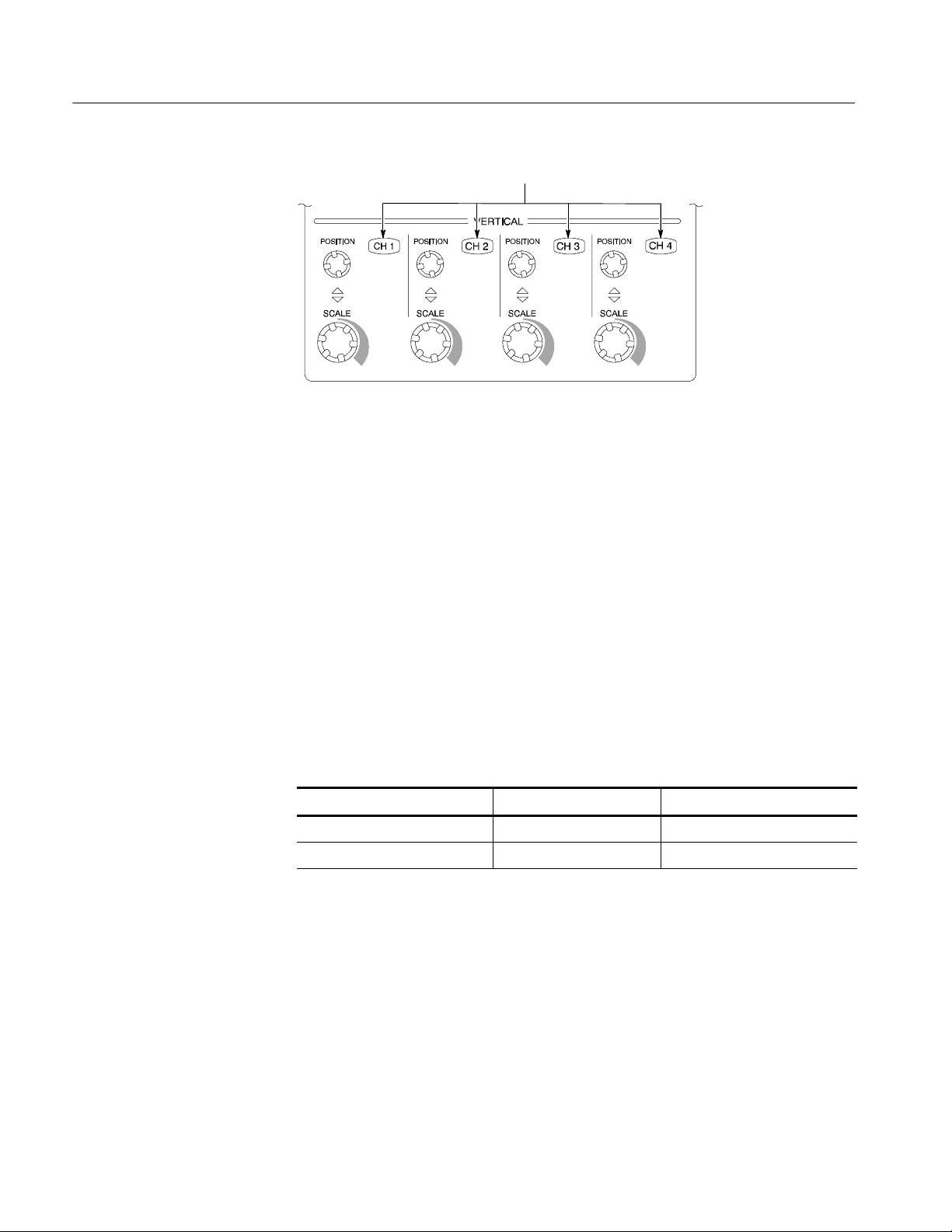
Brief Procedures
Channel buttons
Figure 3- 2: Channel button location
5. Set up the instrument:
H Push the front-panel AUTOSET button. This sets the horizontal and
vertical scale and vertical offset for a usable display and sets the trigger
source to the channel that you are testing.
H Touch the Vert button and then touch Offset. Confirm that the Ch1
Offset is 0V.
6. Verify that the channel is operational: Confirm that the following statements
are true.
H Verify that the vertical scale readout and the waveform amplitude for the
channel under test are as shown in Table 3--1.
Table 3- 1: Vertical settings
Setting TDS6604B, TDS6804B TDS6124C, TDS6154C
Scale 100 mV 100 mV
Waveform amplitude 3 divisions 4.4 divisions
H The front-panel vertical POSITION knob (for the channel you are
testing) moves the signal up and down the screen when rotated.
H Turning the vertical SCALE knob counterclockwise (for the channel you
are testing) decreases the amplitude of the waveform on-screen, turning
the knob clockwise increases the amplitude, and returning the knob to
the original scale setting returns the amplitude to that shown in
Table 3--1 for that scale setting.
3- 4
7. Verify that the channel acquires in all acquisition modes: F rom the
Horiz/Acq menu, select Horizontal/Acquisition Setup . . . . Touch the
TDS6000B & TDS6000C Series Specifications and Performance Verification

Brief Procedures
Acquisition tab in the control window that displays. Touch each of the
acquisition modes and confirm that the following statements are true:
H Sample mode displays an actively acquiring waveform on-screen. (Note
that there is a small amount of noise present on the square wave).
H Peak Detect mode displays an actively acquiring waveform on-screen
with the noise present in Sample mode “peak detected.”
H Hi Res mode displays an actively acquiring waveform on-screen with the
noise that was present in Sample mode reduced.
H Average mode displays an actively acquiring waveform on-screen with
the noise reduced.
H Envelope mode displays an actively acquiring waveform on-screen with
the noise displayed.
H Waveform Database mode displays an actively acquiring waveform
on-screen that is the accumulation of several acquisitions.
Check Horizontal
Operation
8. Test all channels: Repeat steps 2 through 7 until all four input channels are
verified.
9. Remove the test hookup: Disconnect the equipment from the channel input
and the FAST EDGE output.
Equipment
required
Prerequisites None
One SMA cable, such as Tektronix part number 174-1427-xx
One TCA-SMA adapter
1. Initialize the instrument: Push the front-panel DEFAULT SETUP button.
2. Hook up the signal source: Connect the equipment to the CH 1 input as
shown in Figure 3--3.
TDS6000B & TDS6000C Series Specifications and Performance Verification
3- 5
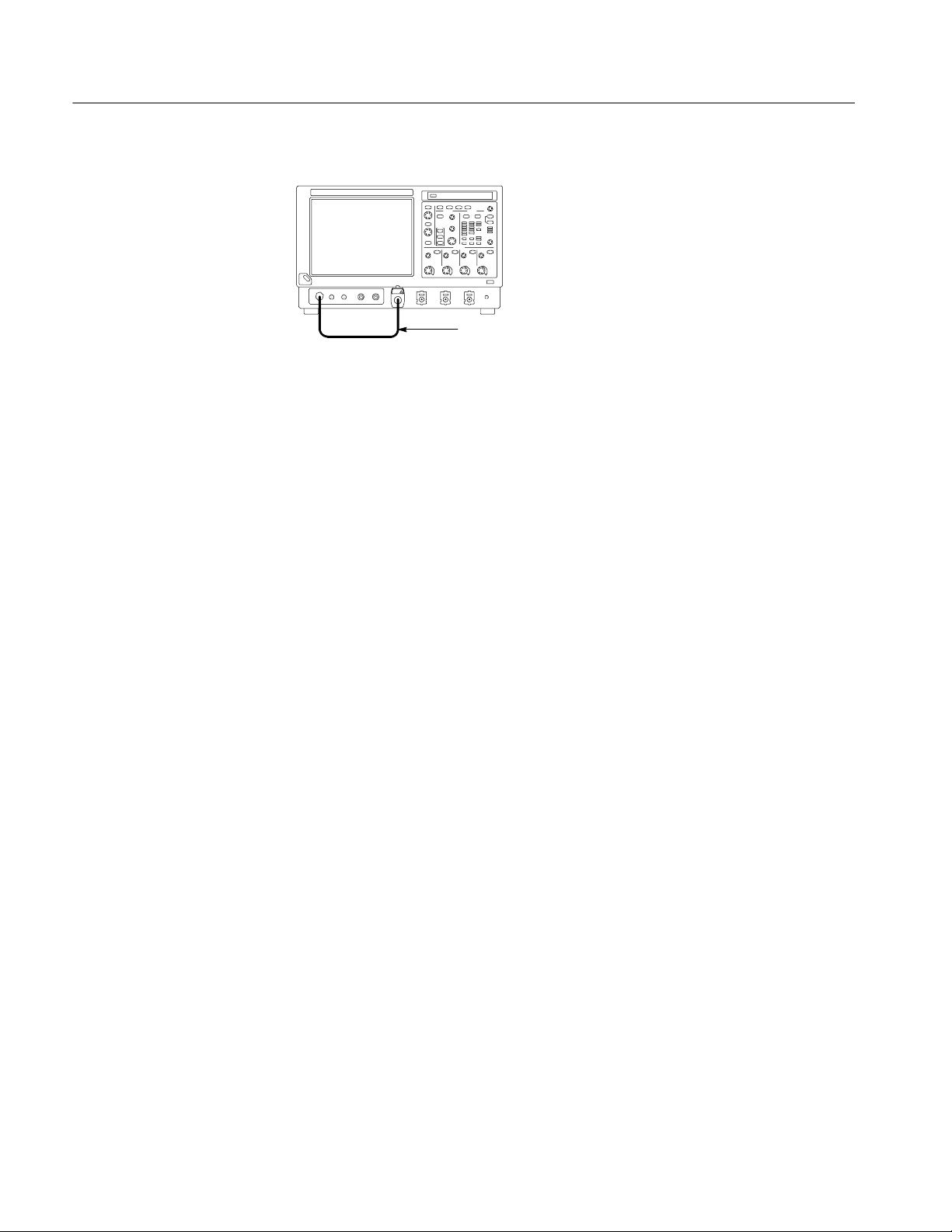
Brief Procedures
Instrument under test
SMA cable from FAST
EDGE output to CH 1
input
Figure 3- 3: Setup for time base test
3. Set up the instrument: Push the front-panel AUTOSET button.
4. Touch the V ert button and then touch Offset. Adjust the Ch1 Offset to
--0.16 V (TDS6000B Series); +80 mV (TDS6000C Series) using the
multipurpose knob.
5. Set the Vertical SCALE to 100 mV per division.
6. Set the time base: Set the horizontal SCALE to 200 s/div. The time-base
readout is displayed at the bottom of the graticule.
7. Verify that the time base operates: Confirm the following statements.
H One period of the square-wave fast edge signal is about five horizontal
divisions on-screen for the 200 s/div horizontal scale setting.
H Rotating the horizontal SCALE knob clockwise expands the waveform
on-screen (more horizontal divisions per waveform period), counterclockwise rotation contracts it, and returning the horizontal scale to
200 s/div returns the period to about five divisions.
H The horizontal POSITION knob positions the signal left and right
on-screen when rotated.
8. Verify horizontal delay:
a. Center a rising edge on screen:
H Set the horizontal POSIT ION knob so that the rising edge where the
waveform is triggered is lined up with the center horizontal
graticule.
3- 6
H Change the horizontal SCALE to 20 s/div. The rising edge of the
waveform should remain near the center graticule and the falling
edge should be off screen.
TDS6000B & TDS6000C Series Specifications and Performance Verification

Brief Procedures
b. Turn on and set horizontal delay:
H From the Horiz/Acq menu, select Horizontal/Acquisition
Setup....
H Touch the Horizontal tab in the control window that displays.
H Touch the Delay Mode button to turn delay on.
H Double-touch the Horiz Delay control in the control window to
display the pop-up keypad. Touch the keypad buttons to set the
horizontal delay to 1.5 ms, and then touch the ENTER key.
c. Verify the waveform: Verify that a falling edge of the waveform is within
a few divisions of center screen.
d. Adjust the horizontal delay: Rotate the upper multipurpose knob to
change the horizontal delay setting. Verify that the falling edge shifts
horizontally. Rotate the front-panel horizontal POSITION knob. Verify
that this knob has the same effect (it also adjusts delay, but only when
delay mode is on).
Check Trigger Operation
e. Verify the delay toggle function:
H Rotate the front-panel horizontal POSITION knob to center the
falling edge horizontally on the screen.
H Change the horizontal SCALE to 40 ns/div. The falling edge of the
waveform should remain on the screen.
H Set horizontal DELAY to -- 8 0 n s . The rising edge should be
2 divisions to the right of the center graticule line.
H Push the front-panel DELAY button several times to toggle delay off
and on and back off again. Verify that the display switches quickly
between two different points in time.
9. Remove the test hookup: Disconnect the equipment from the channel input
and the FAST EDGE output.
Equipment
required
Prerequisites None
One BNC cable, such as Tektronix part number 174-1427-xx
One TCA-SMA TekConnect adapter
1. Initialize the instrument: Push the front-panel DEFAULT SETUP button.
2. Hook up the signal source: Connect the equipment to the CH 1 input as
shown in Figure 3--4.
3. Set up the instrument: Push the front-panel AUTOSET button.
TDS6000B & TDS6000C Series Specifications and Performance Verification
3- 7

Brief Procedures
Instrument under test
SMA cable from FAST
EDGE output to CH 1
input
Figure 3- 4: Setup for trigger test
4. Touch the V ert button and then touch Offset. Adjust the Ch1 Offset to
--0.16 V (TDS6000B Series); +80 mV (TDS6000C Series) using the
multipurpose knob.
5. Set the Vertical SCALE to 100 mV per division.
6. Verify that the main trigger system operates: Confirm that the following
statements are true.
H The trigger level readout for the A (main) trigger system changes with
the trigger-LEVEL knob.
H The trigger-LEVEL knob can trigger and untrigger the square-wave
signal as you rotate it. (Leave the signal untriggered).
H Pushing the front-panel trigger LEVEL knob sets the trigger level to the
50% amplitude point of the signal and triggers the signal that you just
left untriggered. (Leave the signal triggered.)
7. Verify that the delayed trigger system operates:
a. Set up the delayed trigger:
H From the Trig menu, select A→B Sequence . . . . This displays the
A→B Sequence tab of the trigger setup control window.
H Touch the Trig After Time button under A Then B .
H Touch the B Level control in the control window.
b. Confirm that the following statements are true:
3- 8
H The trigger-level readout for the B trigger system changes as you
turn the lower multipurpose knob.
TDS6000B & TDS6000C Series Specifications and Performance Verification

Brief Procedures
H As you rotate the lower multipurpose knob, the square-wave FAST
EDGE signal can become triggered and untriggered. (Leave the
signal triggered.)
c. Verify the delayed trigger counter:
H Set trigger mode to norm.
H Double-touch the Trig Delay control to pop up a numeric keypad for
that control.
H Touch the keypad to enter a trigger delay time of 1000 ms,andthen
touch Enter.
H Verify that the trigger READY indicator on the front panel flashes
about once every second as the waveform is updated on-screen.
8. Remove the test hookup: Disconnect the equipment from the channel input
and the FAST EDGE output.
Perform the Extended Diagnostics
Extended diagnostics and self calibration perform a more detailed functionality
check than the incoming inspection and Power-on diagnostics.
NOTE. Allow a 20-minute warm-up before running the self calibration.
Disconnect any attached signal from the instrument. Then select the Utilities
menu. Run the self calibration followed by the extended diagnostics by first
selecting the Instrument Calibration and then the Instrument Diagnostics tabs.
Results of the tests display on their property pages.
Checking the Underlying
System (Optional)
To check the hardware and Windows software underlying the instrument UI (user
interface), run the CheckIt Utilities from the Windows Start menu:
1. Minimize the instrument application before running the external diagnostics.
From the File menu select Minimize.
2. Touch Start, then touch Programs in the Start Menu. Finally, touch
CheckIt Utilities.
3. From the Go To menu, select and run the tests you want to perform.
4. Check test results. All tests except the Modem and CD-ROM tests should
pass. The CD-ROM test requires data from the CheckIt Utilities CD.
5. Dismiss the CheckIt Utilities: Select Exit in the File menu.
TDS6000B & TDS6000C Series Specifications and Performance Verification
3- 9

Brief Procedures
6. Restart your instrument UI software: On the Quick Launch bar, touch
TekScope.
3- 10
TDS6000B & TDS6000C Series Specifications and Performance Verification

Performance Tests
This section contains a collection of manual procedures for checking that the
TDS6000B & TDS6000C Series oscilloscopes performs as warranted.
The procedures are arranged in four logical groupings: Signal Acquisition System
Checks, Time Base System Checks, Triggering System Checks,andOutput Ports
Checks. They check all the characteristics that are designated as checked in
Specifications. (The characteristics that are checked appear with a n in
Specifications).
STOP. These procedures extend the confidence level pr ovided by the basic
procedures described on page 3--1. The basic procedures should be done first,
then these procedures performed if desired.
Prerequisites
The tests in this section comprise an extensive, valid confirmation of performance and functionality when the following requirements are met:
H The cabinet must be installed on the instrument.
H You must have performed and passed the procedures under Self Tests, found
on page 3--1, and those under Functional Tests, found on page 3--2.
H A signal-path compensation must have been done within the recommended
calibration interval and at a temperature within ±5 _C of the present
operating temperature. A signal-path compensation must have been done at
an ambient humidity within 25% of the current ambient humidity and after
having been at that humidity for at least 4 hours.
H The oscilloscope must have been last adjusted at an ambient temperature
between +20 _C and +30 _C, must have been operating for a warm-up
period of at least 20 minutes, and must be operating at an ambient temperature as listed in Table 1--2 on page 1--4. (The warm-up requirement is usually
met in the course of meeting the Self Tests and Functional Tests prerequisites
listed above).
H Sensors or spitter adapter setups should be supported to avoid stress or
torque when connected to the DUT.
TDS6000B & TDS6000C Series Specifications and Performance Verification
4- 1

Performance Tests
Equipment Required
Table 4- 1: Test equipment
Item number and
description
Procedures starting on page 4--29 use external, traceable signal sources to
directly check warranted characteristics. Table 4--1 lists the required equipment.
Minimum requirements Example Purpose
1. Attenuator,10X
(two required)
2. Attenuator, 5X Ratio: 5X; impedance 50 Ω; connec-
3. Termination, 50 Ω (three
required)
4. Cable, Precision 50 Ω
Coaxial (three required)
5. Connector, Dual-Banana
(two required)
6. Connector, BNC “T” Male BNC-to-dual female BNC Tektronix part number
7. Power divider 50 Ω, 3 SMA female connectors Tektronix part number
8. Generator, DC Calibration
9. Generator, Calibration 500 mV square wave calibrator
10. Timer-counter 25 MHz, 1 s gate Advantest R5360 Checking long--term sample
11. Generator, Sine-Wave 5 kHz to at least 15 GHz. Variable
Ratio: 10X; impedance 50 Ω; connectors: female BNC input, male BNC
output
tors: female BNC input, male BNC
output
Impedance 50 Ω; connectors: female
BNC input, male BNC output
50 Ω, 36 in, male-to-male BNC
connectors
Female BNC-to-dual banana Tektronix part number
Variable amplitude to ±7 V; accuracy
to 0.1%
amplitude; accuracy to 0.25%
amplitude from 60 mV to 2 V
50 Ω. Frequency error <2.0%
p-p
into
Tektronix part number
011-0059-02
Tektronix part number
011-0060-02
Tektronix part number
011-0049-01
Tektronix part number
012-0482-00
103-0090-00
103-0030-00
015-0565-00
Wavetek 9500
Wavetek 9500
Anritsu MG3692A Synthesizer Signal Generator
Options 2, 4, 15
1
1
Signal Attenuation
Signal Attenuation
Signal Termination for
Channel Delay Test
Signal Interconnection
Various Accuracy Tests
UsedtoTestDeltaTime
Measurement Accuracy
Checking Delay Between
Channels
Checking DC Offset, Gain,
Measurement Accuracy, and
Maximum Input Voltage
To check accuracy of Signal
Out
rate and delay time accuracy
Checking Analog Bandwidth,
Trigger Sensitivity, Samplerate, External Clock, and
Delay-Time Accuracy
12. Meter, Level and Power
Sensor
13. Splitter, Power N female (3)
14. Adapter TwoMaleN-to-femaleBNC Tektronix part number
4- 2
Frequency range: 10 MHz to the
instrument bandwidth. Amplitude
range: 6 mV
Frequency range: DC to 8 GHz.
Tracking: >2.0%
p-p
to2V
p-p
TDS6000B & TDS6000C Series Specifications and Performance Verification
Rohde & Schwarz NRVS and
NRV-Z402
Agilent part number 11667A Checking Analog Bandwidth
103-0045-00
Checking Analog Bandwidth
and Trigger Sensitivity
Checking Analog Bandwidth

Table 4- 1: Test equipment ( Cont.)
Item number and
description
Performance Tests
PurposeExampleMinimum requirements
15. Adapter TwoMaleN-to-femaleSMA Amphenol part number
901-294
Checking the sine wave
generator leveling
16. Adapter Male N-to-male SMA Maury part number 8023D1 Checking Analog Bandwidth
17. Adapter (three required) SMA female-to-female Tektronix part number
015-1012-00
18. Adapter (three required) SMA male-to-female BNC Tektronix part number
015-1018-00
19. Adapter
(four required)
SMA male-to-BNC female
SMA female to BNC Male
TCA-BNC or TCA-SMA and
SMA male-to-BNC female
Checking the delay between
channels
Checking the delay between
channels
Signal interconnection
adapter (Tektronix part
number 015-0554-00 or
015-1018-00 or 015-0572-XX)
20. Pulse Generator 500 mV into 50 Ω Wavetek 9500
1,2
UsedtoTestDeltaTime
Measurement Accuracy
21. Cable, Coaxial 50 Ω, 60 in, female-to-female SMA
connectors
22. Cable, Coaxial 50 Ω, 20 in, female-to-female SMA
connectors >18 GHz
23. Cable, Coaxial
(two required)
50 Ω, 20 in, male-to-male SMA
connectors
24. Adapter SMA “T”, male to 2 SMA female Tektronix part number
25. Adapter SMA female to BNC male Tektronix part number
26. Adapter BNC male to female elbow Tektronix part number
27. Termination
Short circuit, SMA connector Tektronix part number
(two required)
28. Attenuator, 2X Ratio: 2X; impedance 50 Ω; connec-
tors: female BNC input, male BNC
output
Tektronix part number
174-1428-00
MegaPhase
TM26-3131-36-4
Tektronix part number
174-1427-00
015-1016-00
015-0572-00
103-0031-00
015-1021-00
Tektronix part number
011-0069-02
Checking TDS6000C Serial
Trigger Baud Rate Limits
Checking Analog Bandwidth
UsedtoTestDeltaTime
Measurement Accuracy
UsedtoTestDeltaTime
Measurement Accuracy
UsedtoTestDeltaTime
Measurement Accuracy
UsedtoTestDeltaTime
Measurement Accuracy
UsedtoTestDeltaTime
Measurement Accuracy
UsedtoTestDeltaTime
Measurement Accuracy, and
channel isolation
29. Data Time Generator Data Time generator Tektronix DTG5334 w/M31 Serial trigger baud rare limits
30. Digital Multimeter Ohms: <60 Ohms Keithley 2000 Checking input impedance
1
Wavetek 9500 with option 100 and an output head (9520, 9530, or 9550) appropriate for the bandwidth of the instrument
being tested.
2
For Delta Time Measurement Accuracy, use a Wavetek 9500 or a pulse generator with a rise time as shown in Table 4- 12
on page 4- 78.
TDS6000B & TDS6000C Series Specifications and Performance Verification
4- 3

Performance Tests
Test Record TDS6000B Series
Photocopy this table and use it to record the performance test results for your
instrument.
TDS6604B and TDS6804B Test Record
Instrument Serial Number: Certificate Number:
Temperature: RH %:
Date of Calibration: Technician:
TDS6604B and TDS6804B performance test Minimum Incoming Outgoing Maximum
DC voltage measurement accuracy (averaged)
CH1 50 mV Vert scale setting,
--5 Div position setting, +0.5 V offset
CH1 50 mV Vert scale setting,
+5 Div position setting, --0.5 V offset
CH1 100 mV Vert scale setting,
--5 Div position setting, +4.8 V offset
CH1 100 mV Vert scale setting,
+5 Div position setting, --4.8 V offset
CH1 1.0 V Vert scale setting,
--5 Div position setting, +2.5 V offset
CH1 1.0 V Vert scale setting,
+5 Div position setting, --2.5 V offset
CH2 50 mV Vert scale setting,
--5 Div position setting, +0.5 V offset
CH2 50 mV Vert scale setting,
+5 Div position setting, --0.5 V offset
CH2 100 mV Vert scale setting,
--5 Div position setting, +4.8 V offset
CH2 100 mV Vert scale setting,
+5 Div position setting, --4.8 V offset
CH2 1.0 V Vert scale setting,
--5 Div position setting, +2.5 V offset
CH2 1.0 V Vert scale setting,
+5 Div position setting, --2.5 V offset
CH3 50 mV Vert scale setting,
--5 Div position setting, +0.5 V offset
CH3 50 mV Vert scale setting,
+5 Div position setting, --0.5 V offset
CH3 100 mV Vert scale setting,
--5 Div position setting, +4.8 V offset
+878.3 mV __________ __________ +921.7 mV
--921.7 mV __________ __________ --878.3 mV
+4.914 V __________ __________ +5.086 V
--5.086 V __________ __________ --4.914 V
+4.125 V __________ __________ +4.875 V
--4.875 V __________ __________ --4.125 V
+878.3 mV __________ __________ +921.7 mV
--921.7 mV __________ __________ --878.3 mV
+4.914 V __________ __________ +5.086 V
--5.086 V __________ __________ --4.914 V
+4.125 V __________ __________ +4.875 V
--4.875 V __________ __________ --4.125 V
+878.3 mV __________ __________ +921.7 mV
--921.7 mV __________ __________ --878.3 mV
+4.914 V __________ __________ +5.086 V
4- 4
TDS6000B & TDS6000C Series Specifications and Performance Verification

TDS6604B and TDS6804B Test Record (cont.)
Instrument Serial Number: Certificate Number:
Temperature: RH %:
Date of Calibration: Technician:
TDS6604B and TDS6804B performance test MaximumOutgoingIncomingMinimum
Performance Tests
CH3 100 mV Vert scale setting,
+5 Div position setting, --4.8 V offset
CH3 1.0 V Vert scale setting,
--5 Div position setting, +2.5 V offset
CH3 1.0 V Vert scale setting,
+5 Div position setting, --2.5 V offset
CH4 50 mV Vert scale setting,
--5 Div position setting, +0.5 V offset
CH4 50 mV Vert scale setting,
+5 Div position setting, --0.5 V offset
CH4 100 mV Vert scale setting,
--5 Div position setting, +4.8 V offset
CH4 100 mV Vert scale setting,
+5 Div position setting, --4.8 V offset
CH4 1.0 V Vert scale setting,
--5 Div position setting, +2.5 V offset
CH4 1.0 V Vert scale setting,
+5 Div position setting, --2.5 V offset
--5.086 V __________ __________ --4.914 V
+4.125 V __________ __________ +4.875 V
--4.875 V __________ __________ --4.125 V
+878.3 mV __________ __________ +921.7 mV
--921.7 mV __________ __________ --878.3 mV
+4.914 V __________ __________ +5.086 V
--5.086 V __________ __________ --4.914 V
+4.125 V __________ __________ +4.875 V
--4.875 V __________ __________ --4.125 V
TDS6000B & TDS6000C Series Specifications and Performance Verification
4- 5

Performance Tests
g
,
V____________________
V
5Divpositionsetting,+
0.5Voffse
t
+73.3mV
_________
_
_________
_
+78.7mV
g
,
V____________________
V--5Divpositionsetting,+
0.5Voffse
t
+14
6.4mV
_________
_
_________
_
+15
7.6mV
g
,
V____________________
V--5Divpositionsetting,+
0.5Voffse
t
+36
4.8mV
_________
_
_________
_
+39
5.2mV
g
,
V____________________
V0Divpositionsettin
g,+
4.5Voffse
t
+73
4.2mV
_________
_
_________
_
+78
5.8mV
g
,
V____________________
V2Divpositionsettin
g,+
4.6Voffse
t
+
1.4692V
_________
_
_________
_
+
1.5708V
g
,
V____________________
V
4Divpositionsetting,+5Voffset
+
3.6822V
_________
_
_________
_
+
3.9178V
g
,
V____________________
V0Divpositionsettin
g,+
2.0Voffse
t
+
5.8260V
_________
_
_________
_
+
6.1740V
g
,
V____________________
V
5Divpositionsetting,+
0.5Voffse
t
+73.3mV
_________
_
_________
_
+78.7mV
g
,
V____________________
V--5Divpositionsetting,+
0.5Voffse
t
+14
6.4mV
_________
_
_________
_
+15
7.6mV
TDS6604B and TDS6804B Test Record (cont.)
Instrument Serial Number: Certificate Number:
Temperature: RH %:
Date of Calibration: Technician:
TDS6604B and TDS6804B performance test MaximumOutgoingIncomingMinimum
DC gain accuracy (averaged)
CH1 10 mV Vert scale setting,
0Divposition setting, 0Voffset
--
-+5 Div position setting, --0.5 V offset
CH1 20 mV Vert scale setting,
0Divposition setting, 0Voffset
-+5 Div position setting, --0.5 V offset
CH1 50 mV Vert scale setting,
0Divposition setting, 0Voffset
-+5 Div position setting, --0.5 V offset
+ 74.1 m
+ 73.3 mV
+ 148.2 m
+ 146.4 mV
+ 370.5 m
+ 364.8 mV
__________
__________
__________
__________
__________
__________
+ 77.9 m
+ 78.7 mV
+ 155.8 m
+ 157.6 mV
+ 389.5 m
+ 395.2 mV
CH1 100 mV Vert scale setting,
0Divposition setting, 0Voffset
0 Div position setting, --4.5 V offset
CH1 200 mV Vert scale setting,
0Divposition setting, 0Voffset
--2 Div position setting, --4.6 V offset
CH1 500 mV Vert scale setting,
0Divposition setting, 0Voffset
--4 Div position setting, --5 V offset
CH1 1.0 V Vert scale setting,
0Divposition setting, 0Voffset
0 Div position setting, --2.0 V offset
CH2 10 mV Vert scale setting,
0Divposition setting, 0Voffset
--
-+5 Div position setting, --0.5 V offset
CH2 20 mV Vert scale setting,
0Divposition setting, 0Voffset
-+5 Div position setting, --0.5 V offset
+ 741.0 m
+ 734.2 mV
+ 1.4820
+ 1.4692 V
+ 3.7050
+ 3.6822 V
+ 7.4100
-- 5.8260 V
+ 74.1 m
+ 73.3 mV
+ 148.2 m
+ 146.4 mV
__________
__________
__________
__________
__________
__________
__________
__________
__________
__________
__________
__________
+ 779.0 m
+ 785.8 mV
+ 1.5580
+ 1.5708 V
+ 3.8950
+ 3.9178 V
+ 7.7900
-- 6.1740 V
+ 77.9 m
+ 78.7 mV
+ 155.8 m
+ 157.6 mV
4- 6
TDS6000B & TDS6000C Series Specifications and Performance Verification
TDS6604B and TDS6804B Test Record (cont.)
g
,
V____________________
V--5Divpositionsetting,+
0.5Voffse
t
+36
4.8mV
_________
_
_________
_
+39
5.2mV
g
,
V____________________
V0Divpositionsettin
g,+
4.5Voffse
t
+73
4.2mV
_________
_
_________
_
+78
5.8mV
g
,
V____________________
V2Divpositionsettin
g,+
4.6Voffse
t
+
1.4692V
_________
_
_________
_
+
1.5708V
g
,
V____________________
V4Divpositionsettin
g,+5Voffset
+
3.6822V
_________
_
_________
_
+
3.9178V
g
,
V____________________
V0Divpositionsettin
g,+
2.0Voffse
t
+
5.8260V
_________
_
_________
_
+
6.1740V
g
,
V____________________
V--5Divpositionsetting,+
0.5Voffse
t
+73.3mV
_________
_
_________
_
+78.7mV
g
,
V____________________
V--5Divpositionsetting,+
0.5Voffse
t
+14
6.4mV
_________
_
_________
_
+15
7.6mV
g
,
V____________________
V
5Divpositionsetting,+
0.5Voffse
t
+36
4.8mV
_________
_
_________
_
+39
5.2mV
g
,
V____________________
V0Divpositionsettin
g,+
4.5Voffse
t
+73
4.2mV
_________
_
_________
_
+78
5.8mV
g
,
V____________________
V2Divpositionsettin
g,+
4.6Voffse
t
+
1.4692V
_________
_
_________
_
+
1.5708V
Instrument Serial Number: Certificate Number:
Temperature: RH %:
Date of Calibration: Technician:
TDS6604B and TDS6804B performance test MaximumOutgoingIncomingMinimum
CH2 50 mV Vert scale setting,
0Divposition setting, 0Voffset
--
+5 Div position setting, --0.5 V offset
CH2 100 mV Vert scale setting,
0Divposition setting, 0Voffset
+ 370.5 m
+ 364.8 mV
+ 741.0 m
__________
__________
Performance Tests
+ 389.5 m
+ 395.2 mV
+ 779.0 m
0 Div position setting, --4.5 V offset
CH2 200 mV Vert scale setting,
0Divposition setting, 0Voffset
--2 Div position setting, --4.6 V offset
CH2 500 mV Vert scale setting,
0Divposition setting, 0Voffset
--4 Div position setting, --5 V offset
CH2 1.0 V Vert scale setting,
0Divposition setting, 0Voffset
0 Div position setting, --2.0 V offset
CH3 10 mV Vert scale setting,
0Divposition setting, 0Voffset
--
+5 Div position setting, --0.5 V offset
CH3 20 mV Vert scale setting,
0Divposition setting, 0Voffset
--
+5 Div position setting, --0.5 V offset
CH3 50 mV Vert scale setting,
0Divposition setting, 0Voffset
--
--
+5 Div position setting, --0.5 V offset
+ 734.2 mV
+ 1.4820
+ 1.4692 V
+ 3.7050
+ 3.6822 V
+ 7.4100
-- 5.8260 V
+ 74.1 m
+ 73.3 mV
+ 148.2 m
+ 146.4 mV
+ 370.5 m
+ 364.8 mV
__________
__________
__________
__________
__________
__________
__________
__________
__________
__________
__________
__________
__________
__________
+ 785.8 mV
+ 1.5580
+ 1.5708 V
+ 3.8950
+ 3.9178 V
+ 7.7900
-- 6.1740 V
+ 77.9 m
+ 78.7 mV
+ 155.8 m
+ 157.6 mV
+ 389.5 m
+ 395.2 mV
CH3 100 mV Vert scale setting,
0Divposition setting, 0Voffset
0 Div position setting, --4.5 V offset
CH3 200 mV Vert scale setting,
0Divposition setting, 0Voffset
--2 Div position setting, --4.6 V offset
TDS6000B & TDS6000C Series Specifications and Performance Verification
+ 741.0 m
+ 734.2 mV
+ 1.4820
+ 1.4692 V
__________
__________
__________
__________
+ 779.0 m
+ 785.8 mV
+ 1.5580
+ 1.5708 V
4- 7
Performance Tests
g
,
V____________________
V4Divpositionsettin
g,+5Voffset
+
3.6822V
_________
_
_________
_
+
3.9178V
g
,
V____________________
V0Divpositionsettin
g,+
2.0Voffse
t
+
5.8260V
_________
_
_________
_
+
6.1740V
g
,
V____________________
V--5Divpositionsetting,+
0.5Voffse
t
+73.3mV
_________
_
_________
_
+78.7mV
g
,
V____________________
V--5Divpositionsetting,+
0.5Voffse
t
+14
6.4mV
_________
_
_________
_
+15
7.6mV
g
,
V____________________
V--5Divpositionsetting,+
0.5Voffse
t
+36
4.8mV
_________
_
_________
_
+39
5.2mV
g
,
V____________________
V0Divpositionsettin
g,+
4.5Voffse
t
+73
4.2mV
_________
_
_________
_
+78
5.8mV
g
,
V____________________
V2Divpositionsettin
g,+
4.6Voffse
t
+
1.4692V
_________
_
_________
_
+
1.5708V
g
,
V____________________
V
4Divpositionsetting,+5Voffset
+
3.6822V
_________
_
_________
_
+
3.9178V
g
,
V____________________
V0Divpositionsettin
g,+
2.0Voffse
t
+
5.8260V
_________
_
_________
_
+
6.1740V
TDS6604B and TDS6804B Test Record (cont.)
Instrument Serial Number: Certificate Number:
Temperature: RH %:
Date of Calibration: Technician:
TDS6604B and TDS6804B performance test MaximumOutgoingIncomingMinimum
CH3 500 mV Vert scale setting,
0Divposition setting, 0Voffset
+ 3.7050
+ 3.8950
--4 Div position setting, --5 V offset
CH3 1.0 V Vert scale setting,
0Divposition setting, 0Voffset
0 Div position setting, --2.0 V offset
CH4 10 mV Vert scale setting,
0Divposition setting, 0Voffset
-+5 Div position setting, --0.5 V offset
CH4 20 mV Vert scale setting,
0Divposition setting, 0Voffset
-+5 Div position setting, --0.5 V offset
CH4 50 mV Vert scale setting,
0Divposition setting, 0Voffset
-+5 Div position setting, --0.5 V offset
CH4 100 mV Vert scale setting,
0Divposition setting, 0Voffset
0 Div position setting, --4.5 V offset
CH4 200 mV Vert scale setting,
0Divposition setting, 0Voffset
+ 3.6822 V
+ 7.4100
-- 5.8260 V
+ 74.1 m
+ 73.3 mV
+ 148.2 m
+ 146.4 mV
+ 370.5 m
+ 364.8 mV
+ 741.0 m
+ 734.2 mV
+ 1.4820
__________
__________
__________
__________
__________
__________
__________
__________
__________
__________
__________
__________
+ 3.9178 V
+ 7.7900
-- 6.1740 V
+ 77.9 m
+ 78.7 mV
+ 155.8 m
+ 157.6 mV
+ 389.5 m
+ 395.2 mV
+ 779.0 m
+ 785.8 mV
+ 1.5580
--2 Div position setting, --4.6 V offset
CH4 500 mV Vert scale setting,
0Divposition setting, 0Voffset
--4 Div position setting, --5 V offset
CH4 1.0 V Vert scale setting,
0Divposition setting, 0Voffset
0 Div position setting, --2.0 V offset
4- 8
TDS6000B & TDS6000C Series Specifications and Performance Verification
+ 1.4692 V
+ 3.7050
+ 3.6822 V
+ 7.4100
-- 5.8260 V
__________
__________
__________
__________
__________
__________
+ 1.5708 V
+ 3.8950
+ 3.9178 V
+ 7.7900
-- 6.1740 V

TDS6604B and TDS6804B Test Record (cont.)
g
,
V--___________________
_
V
0Voffse
t
6.5mV
_________
_
_________
_
+
6.5mV
g
,+5V
V--___________________
_
V0Voffset
25m
V
_________
_
_________
_
+25mV
g
,+5V
V--___________________
_
V0Voffset
65m
V
_________
_
_________
_
+65mV
g
,
V--___________________
_
V0Voffset
115mV
_________
_
_________
_
+115m
V
g
,
V--___________________
_
V0Voffset
6.5mV
_________
_
_________
_
+
6.5mV
g
,
V--___________________
_
V
0Voffse
t
25m
V
_________
_
_________
_
+25mV
g
,+5V
V--___________________
_
V0Voffset
65m
V
_________
_
_________
_
+65mV
g
,
V--___________________
_
V
0Voffse
t
115mV
_________
_
_________
_
+115m
V
g
,
V--___________________
_
V0Voffset
5mV
_________
_
_________
_
+
6.5mV
Instrument Serial Number: Certificate Number:
Temperature: RH %:
Date of Calibration: Technician:
TDS6604B and TDS6804B performance test MaximumOutgoingIncomingMinimum
Offset accuracy
CH1 50 mV Vert scale setting,
+0.5Voffset
--0.5 V offset
CH1 100 mV Vert scale setting,
offset
--5 V offset
CH1 500 mV Vert scale setting,
offset
--5 V offset
+490.0 m
--
--510.0 mV
+4.935
--
--5.065 V
+4.895
--
--5.105 V
__________
__________
__________
__________
__________
__________
Performance Tests
+510.0 m
--490.0 mV
+5.065
--4.935 V
+5.105
--4.895 V
CH1 1.0 V Vert scale setting,
+2.5Voffset
--2.5 V offset
CH2 50 mV Vert scale setting,
+0.5Voffset
--0.5 V offset
CH2 100 mV Vert scale setting,
+5Voffset
--5 V offset
CH2 500 mV Vert scale setting,
offset
--5 V offset
CH2 1.0 V Vert scale setting,
+2.5Voffset
--2.5 V offset
CH3 50 mV Vert scale setting,
+0.5Voffset
--0.5 V offset
+2.365
--
--2.635 V
+490.0 m
--
--510.0 mV
+4.935
--
--5.065 V
+4.895
--
--5.105 V
+2.365
--
--2.635 V
+490.0 m
--6.
--510.0 mV
__________
__________
__________
__________
__________
__________
__________
__________
__________
__________
__________
__________
+2.635
--2.365 V
+510.0 m
--490.0 mV
+5.065
--4.935 V
+5.105
--4.895 V
+2.635
--2.365 V
+510.0 m
--490.0 mV
TDS6000B & TDS6000C Series Specifications and Performance Verification
4- 9

Performance Tests
g
,+5V
V--___________________
_
V0Voffset
25m
V
_________
_
_________
_
+25mV
g
,+5V
V--___________________
_
V0Voffset
65m
V
_________
_
_________
_
+65mV
g
,
V--___________________
_
V0Voffset
115mV
_________
_
_________
_
+115m
V
g
,
V--___________________
_
V0Voffset
6.5mV
_________
_
_________
_
+
6.5mV
g
,+5V
V--___________________
_
V0Voffset
25m
V
_________
_
_________
_
+25mV
g
,+5V
V--___________________
_
V0Voffset
65m
V
_________
_
_________
_
+65mV
g
,
V--___________________
_
V0Voffset
115mV
_________
_
_________
_
+115m
V
TDS6604B and TDS6804B Test Record (cont.)
Instrument Serial Number: Certificate Number:
Temperature: RH %:
Date of Calibration: Technician:
TDS6604B and TDS6804B performance test MaximumOutgoingIncomingMinimum
CH3 100 mV Vert scale setting,
offset
--5 V offset
CH3 500 mV Vert scale setting,
offset
--5 V offset
CH3 1.0 V Vert scale setting,
+2.5Voffset
--2.5 V offset
+4.935
--
--5.065 V
+4.895
--
--5.105 V
+2.365
--
--2.635 V
__________
__________
__________
__________
__________
__________
+5.065
--4.935 V
+5.105
--4.895 V
+2.635
--2.365 V
CH4 50 mV Vert scale setting,
+0.5Voffset
--0.5 V offset
CH4 100 mV Vert scale setting,
offset
--5 V offset
CH4 500 mV Vert scale setting,
offset
--5 V offset
CH4 1.0 V Vert scale setting,
+2.5Voffset
--2.5 V offset
+490.0 m
--
--510.0 mV
+4.935
--
--5.065 V
+4.895
--
--5.105 V
+2.365
--
--2.635 V
__________
__________
__________
__________
__________
__________
__________
__________
+510.0 m
--490.0 mV
+5.065
--4.935 V
+5.105
--4.895 V
+2.635
--2.365 V
4- 10
TDS6000B & TDS6000C Series Specifications and Performance Verification

TDS6604B and TDS6804B Test Record (cont.)
Instrument Serial Number: Certificate Number:
Temperature: RH %:
Date of Calibration: Technician:
TDS6604B and TDS6804B performance test MaximumOutgoingIncomingMinimum
Analog bandwidth
CH1 1 V
500 mV
200 mV
100 mV
50 mV
20 mV
10 mV
3.535 V
2.12 V
848 mV
424 mV
212 mV
84.8 mV
42.4 mV
__________
__________
__________
__________
__________
__________
__________
__________
__________
__________
__________
__________
__________
__________
Performance Tests
N/A
N/A
N/A
N/A
N/A
N/A
N/A
CH2 1 V
500 mV
200 mV
100 mV
50 mV
20 mV
10 mV
CH3 1 V
500 mV
200 mV
100 mV
50 mV
20 mV
10 mV
CH4 1 V
500 mV
200 mV
100 mV
50 mV
20 mV
10 mV
3.535 V
2.12 V
848 V
424 mV
212 mV
84.8 mV
42.4 mV
3.535 V
2.12 V
848 V
424 mV
212 mV
84.8 mV
42.4 mV
3.535 V
2.12 V
848 V
424 mV
212 mV
84.8 mV
42.4 mV
__________
__________
__________
__________
__________
__________
__________
__________
__________
__________
__________
__________
__________
__________
__________
__________
__________
__________
__________
__________
__________
__________
__________
__________
__________
__________
__________
__________
__________
__________
__________
__________
__________
__________
__________
__________
__________
__________
__________
__________
__________
__________
N/A
N/A
N/A
N/A
N/A
N/A
N/A
N/A
N/A
N/A
N/A
N/A
N/A
N/A
N/A
N/A
N/A
N/A
N/A
N/A
N/A
TDS6000B & TDS6000C Series Specifications and Performance Verification
4- 11

Performance Tests
TDS6604B and TDS6804B Test Record (cont.)
Instrument Serial Number: Certificate Number:
Temperature: RH %:
Date of Calibration: Technician:
TDS6604B and TDS6804B performance test MaximumOutgoingIncomingMinimum
Digitally enhanced bandwidth
CH1 1 V
500 mV
200 mV
100 mV
50 mV
20 mV
10 mV
3.535 V
2.12 V
848 mV
424 mV
212 mV
84.8 mV
42.4 mV
__________
__________
__________
__________
__________
__________
__________
__________
__________
__________
__________
__________
__________
__________
N/A
N/A
N/A
N/A
N/A
N/A
N/A
CH2 1 V
500 mV
200 mV
100 mV
50 mV
20 mV
10 mV
CH3 1 V
500 mV
200 mV
100 mV
50 mV
20 mV
10 mV
CH4 1 V
500 mV
200 mV
100 mV
50 mV
20 mV
10 mV
3.535 V
2.12 V
848 V
424 mV
212 mV
84.8 mV
42.4 mV
3.535 V
2.12 V
848 V
424 mV
212 mV
84.8 mV
42.4 mV
3.535 V
2.12 V
848 V
424 mV
212 mV
84.8 mV
42.4 mV
__________
__________
__________
__________
__________
__________
__________
__________
__________
__________
__________
__________
__________
__________
__________
__________
__________
__________
__________
__________
__________
__________
__________
__________
__________
__________
__________
__________
__________
__________
__________
__________
__________
__________
__________
__________
__________
__________
__________
__________
__________
__________
N/A
N/A
N/A
N/A
N/A
N/A
N/A
N/A
N/A
N/A
N/A
N/A
N/A
N/A
N/A
N/A
N/A
N/A
N/A
N/A
N/A
4- 12
TDS6000B & TDS6000C Series Specifications and Performance Verification
Performance Tests
TDS6604B and TDS6804B Test Record (cont.)
Instrument Serial Number: Certificate Number:
Temperature: RH %:
Date of Calibration: Technician:
TDS6604B and TDS6804B performance test MaximumOutgoingIncomingMinimum
Delay between channels N/A __________ __________ 30 ps
Channel isolation 1.5 GHz
100 mV
CH 1
CH 2
CH 3
CH 4
50 mV
CH 1
CH 2
CH 3
CH 4
10 mV
CH 1
CH 2
CH 3
CH 4
full bandwidth
100 mV
CH 1
CH 2
CH 3
CH 4
50 mV
CH 1
CH 2
CH 3
CH 4
10 mV
CH 1
CH 2
CH 3
CH 4
N/A
N/A
N/A
N/A
N/A
N/A
N/A
N/A
N/A
N/A
N/A
N/A
N/A
N/A
N/A
N/A
N/A
N/A
N/A
N/A
N/A
N/A
N/A
N/A
__________
__________
__________
__________
__________
__________
__________
__________
__________
__________
__________
__________
__________
__________
__________
__________
__________
__________
__________
__________
__________
__________
__________
__________
__________
__________
__________
__________
__________
__________
__________
__________
__________
__________
__________
__________
__________
__________
__________
__________
__________
__________
__________
__________
__________
__________
__________
__________
0.125 divisions
0.125 divisions
0.125 divisions
0.125 divisions
0.125 divisions
0.125 divisions
0.125 divisions
0.125 divisions
0.125 divisions
0.125 divisions
0.125 divisions
0.125 divisions
0.5 divisions
0.5 divisions
0.5 divisions
0.5 divisions
0.5 divisions
0.5 divisions
0.5 divisions
0.5 divisions
0.5 divisions
0.5 divisions
0.5 divisions
0.5 divisions
TDS6000B & TDS6000C Series Specifications and Performance Verification
4- 13

Performance Tests
TDS6604B and TDS6804B Test Record (cont.)
Instrument Serial Number: Certificate Number:
Temperature: RH %:
Date of Calibration: Technician:
TDS6604B and TDS6804B performance test MaximumOutgoingIncomingMinimum
Input impedance
CH1 10 mV
CH1 100 mV
CH2 10 mV
CH2 100 mV
CH3 10 mV
CH3 100 mV
CH4 10 mV
CH4 100 mV
Time base system
Long term sample rate, delay time, and internal
reference accuracy
Delta time measurement Ch 1 N/A __________ __________ ≤0.03 ns
Ch 2 N/A __________ __________ ≤0.03 ns
Ch 3
Ch 4
Trigger system accuracy
Time accuracy for pulse, glitch, timeout, and
Width, Hor. scale ≤ 1 s
Lower Limit
Upper Limit
48.75 Ω
48.75 Ω
48.75 Ω
48.75 Ω
48.75 Ω
48.75 Ω
48.75 Ω
48.75 Ω
9999.975 kHz __________ __________ 10000.025 kHz
N/A
N/A
3.5 ns
3.5 ns
__________
__________
__________
__________
__________
__________
__________
__________
__________ __________ ≤0.03 ns
__________ __________ ≤0.03 ns
__________
__________
__________
__________
__________
__________
__________
__________
__________
__________
__________
__________
51.25 Ω
51.25 Ω
51.25 Ω
51.25 Ω
51.25 Ω
51.25 Ω
51.25 Ω
51.25 Ω
6.5 ns
6.5 ns
Time accuracy for pulse, glitch, timeout, and
width, Hor. scale > 1 s
Lower Limit
Upper Limit
Probe Fast Edge (Probe compensation on some models) output signal
Frequency 950 Hz __________ __________ 1.050 kHz
Voltage (difference) 264 mV __________ __________ 396 mV
4- 14
TDS6000B & TDS6000C Series Specifications and Performance Verification
1.9 s
1.9 s
__________
__________
__________
__________
2.1 s
2.1 s

Performance Tests
TDS6604B and TDS6804B Test Record (cont.)
Instrument Serial Number: Certificate Number:
Temperature: RH %:
Date of Calibration: Technician:
TDS6604B and TDS6804B performance test MaximumOutgoingIncomingMinimum
Serial trigger (Option ST only)
Baud rate limits
Serial word recognizer
Signal path 0, Pattern matching 1
Trigger 1 UI before 0
Trigger on 0
Trigger 1 UI after 0
Signal path 1, Pattern matching 1
Trigger 1 UI before 1
Trigger on 1
Trigger 1 UI after 1
Pattern matching 0
Position 1
Position 2
Position 3
Position 4
Position 5
Position 6
Position 7
Position 8
Position 9
Position 10
Position 11
Position 12
Position 13
Position 14
Position 15
Position 16
Position 17
Position 18
Position 19
Position 20
Position 21
Position 22
Position 23
Position 24
Position 25
Position 26
Position 27
Position 28
Position 29
Position 30
Position 31
Position 32
Clock recovery frequency range Pass __________ __________ N/A
Pass
Pass
Pass
Pass
Pass
Pass
Pass
Pass
Pass
Pass
Pass
Pass
Pass
Pass
Pass
Pass
Pass
Pass
Pass
Pass
Pass
Pass
Pass
Pass
Pass
Pass
Pass
Pass
Pass
Pass
Pass
Pass
Pass
Pass
Pass
Pass
Pass
Pass
__________
__________
__________
__________
__________
__________
__________
__________
__________
__________
__________
__________
__________
__________
__________
__________
__________
__________
__________
__________
__________
__________
__________
__________
__________
__________
__________
__________
__________
__________
__________
__________
__________
__________
__________
__________
__________
__________
__________
__________
__________
__________
__________
__________
__________
__________
__________
__________
__________
__________
__________
__________
__________
__________
__________
__________
__________
__________
__________
__________
__________
__________
__________
__________
__________
__________
__________
__________
__________
__________
__________
__________
__________
__________
__________
__________
__________
__________
__________
__________
__________
__________
N/A
N/A
N/A
N/A
N/A
N/A
N/A
N/A
N/A
N/A
N/A
N/A
N/A
N/A
N/A
N/A
N/A
N/A
N/A
N/A
N/A
N/A
N/A
N/A
N/A
N/A
N/A
N/A
N/A
N/A
N/A
N/A
N/A
N/A
N/A
N/A
N/A
N/A
TDS6000B & TDS6000C Series Specifications and Performance Verification
4- 15

Performance Tests
Test Record TDS6000C Series
Photocopy this table and use it to record the performance test results for your
instrument.
TDS6124C and TDS6154C Test Record
Instrument Serial Number: Certificate Number:
Temperature: RH %:
Date of Calibration: Technician:
TDS6124C and TDS6154C performance test Minimum Incoming Outgoing Maximum
DC voltage measurement accuracy (averaged)
CH1 50 mV Vert scale setting,
--5 Div position setting, +0.25 V offset
CH1 50 mV Vert scale setting,
+5 Div position setting, --0.25 V offset
CH1 100 mV Vert scale setting,
--5 Div position setting, +4.0 V offset
CH1 100 mV Vert scale setting,
+5 Div position setting, --4.0 V offset
CH1 1.0 V Vert scale setting,
--5 Div position setting, 0 V offset
CH1 1.0 V Vert scale setting,
+5 Div position setting, 0 V offset
CH2 50 mV Vert scale setting,
--5 Div position setting, +0.25 V offset
CH2 50 mV Vert scale setting,
+5 Div position setting, --0.25 V offset
CH2 100 mV Vert scale setting,
--5 Div position setting, +4.0 V offset
CH2 100 mV Vert scale setting,
+5 Div position setting, --4.0 V offset
CH2 1.0 V Vert scale setting,
--5 Div position setting, 0 V offset
CH2 1.0 V Vert scale setting,
+5 Div position setting, 0 V offset
CH3 50 mV Vert scale setting,
--5 Div position setting, +0.25 V offset
CH3 50 mV Vert scale setting,
+5 Div position setting, --0.25 V offset
CH3 100 mV Vert scale setting,
--5 Div position setting, +4.0 V offset
+634.8 mV __________ __________ +665.2 mV
--665.2 mV __________ __________ --634.8 mV
+4.843 V __________ __________ +4.957 V
--4.957 V __________ __________ --4.843 V
+5.278 V __________ __________ +5.723 V
--5.723 V __________ __________ --5.278 V
+634.8 mV __________ __________ +665.2 mV
--665.2 mV __________ __________ --634.8 mV
+4.843 V __________ __________ +4.957 V
--4.957 V __________ __________ --4.843 V
+5.278 V __________ __________ +5.723 V
--5.723 V __________ __________ --5.278 V
+634.8 mV __________ __________ +665.2 mV
--665.2 mV __________ __________ --634.8 mV
+4.843 V __________ __________ +4.957 V
4- 16
TDS6000B & TDS6000C Series Specifications and Performance Verification

TDS6124C and TDS6154C Test Record (cont.)
Instrument Serial Number: Certificate Number:
Temperature: RH %:
Date of Calibration: Technician:
TDS6124C and TDS6154C performance test MaximumOutgoingIncomingMinimum
Performance Tests
CH3 100 mV Vert scale setting,
+5 Div position setting, --4.0 V offset
CH3 1.0 V Vert scale setting,
--5 Div position setting, 0 V offset
CH3 1.0 V Vert scale setting,
+5 Div position setting, 0 V offset
CH4 50 mV Vert scale setting,
--5 Div position setting, +0.25 V offset
CH4 50 mV Vert scale setting,
+5 Div position setting, --0.25 V offset
CH4 100 mV Vert scale setting,
--5 Div position setting, +4.0V offset
CH4 100 mV Vert scale setting,
+5 Div position setting, --4.0 V offset
CH4 1.0 V Vert scale setting,
--5 Div position setting, 0 V offset
CH4 1.0 V Vert scale setting,
+5 Div position setting, 0 V offset
--4.957 V __________ __________ --4.843 V
+5.278 V __________ __________ +5.723 V
--5.723 V __________ __________ --5.278 V
+634.8 mV __________ __________ +665.2 mV
--665.2 mV __________ __________ --634.8 mV
+4.843 V __________ __________ +4.957 V
--4.957 V __________ __________ --4.843 V
+5.278 V __________ __________ +5.723 V
--5.723 V __________ __________ --5.278 V
TDS6000B & TDS6000C Series Specifications and Performance Verification
4- 17

Performance Tests
g
,
V____________________
V
5Divpositionsetting,+
0.45Voffset
+74.48m
V
_________
_
_________
_
+77.52m
V
g
,
V____________________
V--5Divpositionsetting,+
0.4Voffse
t
+14
9.0mV
_________
_
_________
_
+15
5.0mV
g
,
V____________________
V--5Divpositionsetting,+
0.25Voffset
+37
2.4mV
_________
_
_________
_
+38
7.6mV
g
,
V____________________
V--5Divpositionsetting,+
4.5Voffse
t
+74
4.8mV
_________
_
_________
_
+77
5.2mV
g
,
V____________________
V--2Divpositionsetting,+
4.0Voffse
t
+
1.490
V
_________
_
_________
_
+
1.550
V
g
,
V____________________
V--3Divpositionsetting,+
2.0Voffse
t
+
3.734
V
_________
_
_________
_
+
3.876
V
g
,
V____________________
V
2Divpositionsetting,0Voffse
t
+
6.860
V
_________
_
_________
_
+
7.140
V
TDS6124C and TDS6154C Test Record (cont.)
Instrument Serial Number: Certificate Number:
Temperature: RH %:
Date of Calibration: Technician:
TDS6124C and TDS6154C performance test MaximumOutgoingIncomingMinimum
DC gain accuracy (averaged)
CH1 10 mV/div vert scale setting,
0Divposition setting, 0Voffset
--
-+5 Div position setting, --0.45 V offset
CH1 20 mV/div Vert scale setting,
0Divposition setting, 0Voffset
-+5 Div position setting, --0.4 V offset
CH1 50 mV/div Vert scale setting,
0Divposition setting, 0Voffset
-+5 Div position setting, --0.25 V offset
+ 74.48 m
+ 74.48 mV
+ 149.0 m
+ 149.0 mV
+ 372.4 m
+ 372.4 mV
__________
__________
__________
__________
__________
__________
+ 77.52 m
+ 77.52 mV
+ 155.0 m
+ 155.0 mV
+ 387.6 m
+ 387.6 mV
CH1 99.5 mV/div Vert scale setting,
0 Div position setting, 0 V offset
CH1 100 mV/div Vert scale setting,
0Divposition setting, 0Voffset
-+5 Div position setting, --4.5 V offset
CH1 200 mV/div Vert scale setting,
0Divposition setting, 0Voffset
-+2 Div position setting, --4.0 V offset
CH1 500 mV/div Vert scale setting,
0Divposition setting, 0Voffset
-+3 Div position setting, --2.0 V offset
CH1 1 V/div Vert scale setting,
0Divposition setting, 0Voffset
--2 Div position setting, 0 V offset
+ 741.1 mV __________ __________ + 771.3 mV
+ 744.8 m
+ 744.8 mV
+ 1.490
+ 1.490 V
+ 3.724
+ 3.734 V
+ 7.448
+ 6.860 V
__________
__________
__________
__________
__________
__________
__________
__________
+ 775.2 m
+ 775.2 mV
+ 1.550
+ 1.550 V
+ 3.876
+ 3.876 V
+ 7.752
+ 7.140 V
4- 18
TDS6000B & TDS6000C Series Specifications and Performance Verification

TDS6124C and TDS6154C Test Record (cont.)
g
,
V____________________
V--5Divpositionsetting,+
0.45Voffset
+74.48m
V
_________
_
_________
_
+77.52m
V
g
,
V____________________
V--5Divpositionsetting,+
0.4Voffse
t
+14
9.0mV
_________
_
_________
_
+15
5.0mV
g
,
V____________________
V--5Divpositionsetting,+
0.25Voffset
+37
2.4mV
_________
_
_________
_
+38
7.6mV
g
,
V____________________
V--5Divpositionsetting,+
4.5Voffse
t
+74
4.8mV
_________
_
_________
_
+77
5.2mV
g
,
V____________________
V--2Divpositionsetting,+
4.0Voffse
t
+
1.490
V
_________
_
_________
_
+
1.550
V
g
,
V____________________
V--3Divpositionsetting,+
2.0Voffse
t
+
3.734
V
_________
_
_________
_
+
3.876
V
g
,
V____________________
V
2Divpositionsetting,0Voffse
t
+
6.860
V
_________
_
_________
_
+
7.140
V
Instrument Serial Number: Certificate Number:
Temperature: RH %:
Date of Calibration: Technician:
TDS6124C and TDS6154C performance test MaximumOutgoingIncomingMinimum
CH2 10 mV/div vert scale setting,
0Divposition setting, 0Voffset
--
+5 Div position setting, --0.45 V offset
CH2 20 mV/div Vert scale setting,
0Divposition setting, 0Voffset
--
+5 Div position setting, --0.4 V offset
CH2 50 mV/div Vert scale setting,
0Divposition setting, 0Voffset
--
+5 Div position setting, --0.25 V offset
+ 74.48 m
+ 74.48 mV
+ 149.0 m
+ 149.0 mV
+ 372.4 m
+ 372.4 mV
__________
__________
__________
__________
__________
__________
Performance Tests
+ 77.52 m
+ 77.52 mV
+ 155.0 m
+ 155.0 mV
+ 387.6 m
+ 387.6 mV
CH2 99.5 mV/div Vert scale setting,
0 Div position setting, 0 V offset
CH2 100 mV/div Vert scale setting,
0Divposition setting, 0Voffset
--
+5 Div position setting, --4.5 V offset
CH2 200 mV/div Vert scale setting,
0Divposition setting, 0Voffset
--
+2 Div position setting, --4.0 V offset
CH2 500 mV/div Vert scale setting,
0Divposition setting, 0Voffset
--
+3 Div position setting, --2.0 V offset
CH2 1 V/div Vert scale setting,
0Divposition setting, 0Voffset
--2 Div position setting, 0 V offset
+ 741.1 mV __________ __________ + 771.3 mV
+ 744.8 m
+ 744.8 mV
+ 1.490
+ 1.490 V
+ 3.724
+ 3.734 V
+ 7.448
+ 6.860 V
__________
__________
__________
__________
__________
__________
__________
__________
+ 775.2 m
+ 775.2 mV
+ 1.550
+ 1.550 V
+ 3.876
+ 3.876 V
+ 7.752
+ 7.140 V
TDS6000B & TDS6000C Series Specifications and Performance Verification
4- 19
Performance Tests
g
,
V____________________
V--5Divpositionsetting,+
0.45Voffset
+74.48m
V
_________
_
_________
_
+77.52m
V
g
,
V____________________
V--5Divpositionsetting,+
0.4Voffse
t
+14
9.0mV
_________
_
_________
_
+15
5.0mV
g
,
V____________________
V--5Divpositionsetting,+
0.25Voffset
+37
2.4mV
_________
_
_________
_
+38
7.6mV
g
,
V____________________
V--5Divpositionsetting,+
4.5Voffse
t
+74
4.8mV
_________
_
_________
_
+77
5.2mV
g
,
V____________________
V--2Divpositionsetting,+
4.0Voffse
t
+
1.490
V
_________
_
_________
_
+
1.550
V
g
,
V____________________
V--3Divpositionsetting,+
2.0Voffse
t
+
3.734
V
_________
_
_________
_
+
3.876
V
g
,
V____________________
V
2Divpositionsetting,0Voffse
t
+
6.860
V
_________
_
_________
_
+
7.140
V
TDS6124C and TDS6154C Test Record (cont.)
Instrument Serial Number: Certificate Number:
Temperature: RH %:
Date of Calibration: Technician:
TDS6124C and TDS6154C performance test MaximumOutgoingIncomingMinimum
CH3 10 mV/div vert scale setting,
0Divposition setting, 0Voffset
-+5 Div position setting, --0.45 V offset
CH3 20 mV/div Vert scale setting,
0Divposition setting, 0Voffset
-+5 Div position setting, --0.4 V offset
CH3 50 mV/div Vert scale setting,
0Divposition setting, 0Voffset
-+5 Div position setting, --0.25 V offset
+ 74.48 m
+ 74.48 mV
+ 149.0 m
+ 149.0 mV
+ 372.4 m
+ 372.4 mV
__________
__________
__________
__________
__________
__________
+ 77.52 m
+ 77.52 mV
+ 155.0 m
+ 155.0 mV
+ 387.6 m
+ 387.6 mV
CH3 99.5 mV/div Vert scale setting,
0 Div position setting, 0 V offset
CH3 100 mV/div Vert scale setting,
0Divposition setting, 0Voffset
-+5 Div position setting, --4.5 V offset
CH3 200 mV/div Vert scale setting,
0Divposition setting, 0Voffset
-+2 Div position setting, --4.0 V offset
CH3 500 mV/div Vert scale setting,
0Divposition setting, 0Voffset
-+3 Div position setting, --2.0 V offset
CH3 1 V/div Vert scale setting,
0Divposition setting, 0Voffset
--2 Div position setting, 0 V offset
+ 741.1 mV __________ __________ + 771.3 mV
+ 744.8 m
+ 744.8 mV
+ 1.490
+ 1.490 V
+ 3.724
+ 3.734 V
+ 7.448
+ 6.860 V
__________
__________
__________
__________
__________
__________
__________
__________
+ 775.2 m
+ 775.2 mV
+ 1.550
+ 1.550 V
+ 3.876
+ 3.876 V
+ 7.752
+ 7.140 V
4- 20
TDS6000B & TDS6000C Series Specifications and Performance Verification

TDS6124C and TDS6154C Test Record (cont.)
g
,
V____________________
V--5Divpositionsetting,+
0.45Voffset
+74.48m
V
_________
_
_________
_
+77.52m
V
g
,
V____________________
V--5Divpositionsetting,+
0.4Voffse
t
+14
9.0mV
_________
_
_________
_
+15
5.0mV
g
,
V____________________
V--5Divpositionsetting,+
0.25Voffset
+37
2.4mV
_________
_
_________
_
+38
7.6mV
g
,
V____________________
V--5Divpositionsetting,+
4.5Voffse
t
+74
4.8mV
_________
_
_________
_
+77
5.2mV
g
,
V____________________
V--2Divpositionsetting,+
4.0Voffse
t
+
1.490
V
_________
_
_________
_
+
1.550
V
g
,
V____________________
V--3Divpositionsetting,+
2.0Voffse
t
+
3.734
V
_________
_
_________
_
+
3.876
V
g
,
V____________________
V
2Divpositionsetting,0Voffse
t
+
6.860
V
_________
_
_________
_
+
7.140
V
Instrument Serial Number: Certificate Number:
Temperature: RH %:
Date of Calibration: Technician:
TDS6124C and TDS6154C performance test MaximumOutgoingIncomingMinimum
CH4 10 mV/div vert scale setting,
0Divposition setting, 0Voffset
--
+5 Div position setting, --0.45 V offset
CH4 20 mV/div Vert scale setting,
0Divposition setting, 0Voffset
--
+5 Div position setting, --0.4 V offset
CH4 50 mV/div Vert scale setting,
0Divposition setting, 0Voffset
--
+5 Div position setting, --0.25 V offset
+ 74.48 m
+ 74.48 mV
+ 149.0 m
+ 149.0 mV
+ 372.4 m
+ 372.4 mV
__________
__________
__________
__________
__________
__________
Performance Tests
+ 77.52 m
+ 77.52 mV
+ 155.0 m
+ 155.0 mV
+ 387.6 m
+ 387.6 mV
CH4 99.5 mV/div Vert scale setting,
0 Div position setting, 0 V offset
CH4 100 mV/div Vert scale setting,
0Divposition setting, 0Voffset
--
+5 Div position setting, --4.5 V offset
CH4 200 mV/div Vert scale setting,
0Divposition setting, 0Voffset
--
+2 Div position setting, --4.0 V offset
CH4 500 mV/div Vert scale setting,
0Divposition setting, 0Voffset
--
+3 Div position setting, --2.0 V offset
CH4 1 V/div Vert scale setting,
0Divposition setting, 0Voffset
--2 Div position setting, 0 V offset
+ 741.1 mV __________ __________ + 771.3 mV
+ 744.8 m
+ 744.8 mV
+ 1.490
+ 1.490 V
+ 3.724
+ 3.734 V
+ 7.448
+ 6.860 V
__________
__________
__________
__________
__________
__________
__________
__________
+ 775.2 m
+ 775.2 mV
+ 1.550
+ 1.550 V
+ 3.876
+ 3.876 V
+ 7.752
+ 7.140 V
TDS6000B & TDS6000C Series Specifications and Performance Verification
4- 21
Performance Tests
g
,
V--___________________
_
V
5Voffse
t,0positionsettin
g--4.541V___________________
_--4.459
V
g
,
V--___________________
_
V
0Voffse
t,+2positionsetting--4.45V____________________--4.35V
g
,
V--___________________
_
V
0Voffse
t,+3positionsetting--3.577V___________________
_--3.423
V
TDS6124C and TDS6154C Test Record (cont.)
Instrument Serial Number: Certificate Number:
Temperature: RH %:
Date of Calibration: Technician:
TDS6124C and TDS6154C performance test MaximumOutgoingIncomingMinimum
Offset accuracy
CH1 10 mV Vert scale setting,
+450 mV offset, --5 position setting
--450 mV offset, +5 position setting
CH1 20 mV Vert scale setting,
+400 mV offset, --5 position setting
--400 mV offset, +5 position setting
CH1 50 mV Vert scale setting,
+0.25 V offset, --5 position setting
--0.25 V offset, +5 position setting
+495.8 mV
--504.2 mV
+494.8 mV
--505.2 mV
+491.8 mV
--508.2 mV
__________
__________
__________
__________
__________
__________
__________
__________
__________
__________
__________
__________
+504.2 mV
--495.8 mV
+505.2 mV
--494.8 mV
+508.2 mV
--491.8 mV
CH1 100 mV Vert scale setting,
+4.5Voffset, 0 position setting
--
--4.
CH1 200 mV Vert scale setting,
+4.0Voffset, --2 position setting
--
--4.
CH1 500 mV Vert scale setting,
+2.0Voffset, --3 position setting
--
--2.
CH2 10 mV Vert scale setting,
+450 mV offset, --5 position setting
--450 mV offset, +5 position setting
CH2 20 mV Vert scale setting,
+400 mV offset, --5 position setting
--400 mV offset, +5 position setting
CH2 50 mV Vert scale setting,
+0.25 V offset, --5 position setting
--0.25 V offset, +5 position setting
+4.459
+4.35
+3.423
+495.8 mV
--504.2 mV
+494.8 mV
--505.2 mV
+491.8 mV
--508.2 mV
__________
__________
__________
__________
__________
__________
__________
__________
__________
__________
__________
__________
+4.541
--
+4.45
--
+3.577
--
+504.2 mV
--495.8 mV
+505.2 mV
--494.8 mV
+508.2 mV
--491.8 mV
4- 22
TDS6000B & TDS6000C Series Specifications and Performance Verification

TDS6124C and TDS6154C Test Record (cont.)
g
,
V--___________________
_
V
5Voffse
t,0positionsettin
g--4.541V___________________
_--4.459
V
g
,
V--___________________
_
V
0Voffse
t,+2positionsetting--4.45V____________________--4.35V
g
,
V--___________________
_
V
0Voffse
t,+3positionsetting--3.577V___________________
_--3.423
V
g
,
V--___________________
_
V
5Voffse
t,0positionsettin
g--4.541V___________________
_--4.459
V
g
,
V--___________________
_
V
0Voffse
t,+2positionsetting--4.45V____________________--4.35V
g
,
V--___________________
_
V
0Voffse
t,+3positionsetting--3.577V___________________
_--3.423
V
Instrument Serial Number: Certificate Number:
Temperature: RH %:
Date of Calibration: Technician:
TDS6124C and TDS6154C performance test MaximumOutgoingIncomingMinimum
CH2 100 mV Vert scale setting,
+4.5Voffset, 0 position setting
--
--4.
CH2 200 mV Vert scale setting,
+4.0Voffset, --2 position setting
--
--4.
CH2 500 mV Vert scale setting,
+2.0Voffset, --3 position setting
--
--2.
+4.459
+4.35
+3.423
Performance Tests
+4.541
--
+4.45
--
+3.577
--
CH3 10 mV Vert scale setting,
+450 mV offset, --5 position setting
--450 mV offset, +5 position setting
CH3 20 mV Vert scale setting,
+400 mV offset, --5 position setting
--400 mV offset, +5 position setting
CH3 50 mV Vert scale setting,
+0.25 V offset, --5 position setting
--0.25 V offset, +5 position setting
CH3 100 mV Vert scale setting,
+4.5Voffset, 0 position setting
--
--4.
CH3 200 mV Vert scale setting,
+4.0Voffset, --2 position setting
--
--4.
CH3 500 mV Vert scale setting,
+2.0Voffset, --3 position setting
--
--2.
+495.8 mV
--504.2 mV
+494.8 mV
--505.2 mV
+491.8 mV
--508.2 mV
+4.459
+4.35
+3.423
__________
__________
__________
__________
__________
__________
__________
__________
__________
__________
__________
__________
+504.2 mV
--495.8 mV
+505.2 mV
--494.8 mV
+508.2 mV
--491.8 mV
+4.541
--
+4.45
--
+3.577
--
CH4 10 mV Vert scale setting,
+450 mV offset, --5 position setting
--450 mV offset, +5 position setting
TDS6000B & TDS6000C Series Specifications and Performance Verification
+495.8 mV
--504.2 mV
__________
__________
__________
__________
+504.2 mV
--495.8 mV
4- 23
Performance Tests
g
,
V--___________________
_
V
5Voffse
t,0positionsettin
g--4.541V___________________
_--4.459
V
g
,
V--___________________
_
V
0Voffse
t,+2positionsetting--4.45V____________________--4.35V
g
,
V--___________________
_
V
0Voffse
t,+3positionsetting--3.577V___________________
_--3.423
V
TDS6124C and TDS6154C Test Record (cont.)
Instrument Serial Number: Certificate Number:
Temperature: RH %:
Date of Calibration: Technician:
TDS6124C and TDS6154C performance test MaximumOutgoingIncomingMinimum
CH4 20 mV Vert scale setting,
+400 mV offset, --5 position setting
--400 mV offset, +5 position setting
CH4 50 mV Vert scale setting,
+0.25 V offset, --5 position setting
--0.25 V offset, +5 position setting
CH4 100 mV Vert scale setting,
+4.5Voffset, 0 position setting
--
--4.
+494.8 mV
--505.2 mV
+491.8 mV
--508.2 mV
+4.459
__________
__________
__________
__________
__________
__________
__________
__________
+505.2 mV
--494.8 mV
+508.2 mV
--491.8 mV
+4.541
--
CH4 200 mV Vert scale setting,
+4.0Voffset, --2 position setting
--
--4.
CH4 500 mV Vert scale setting,
+2.0Voffset, --3 position setting
--
--2.
+4.35
+3.423
+4.45
--
+3.577
--
4- 24
TDS6000B & TDS6000C Series Specifications and Performance Verification

TDS6124C and TDS6154C Test Record (cont.)
Instrument Serial Number: Certificate Number:
Temperature: RH %:
Date of Calibration: Technician:
TDS6124C and TDS6154C performance test MaximumOutgoingIncomingMinimum
Analog bandwidth
CH1 1 V
500 mV
200 mV
100 mV
50 mV
20 mV
10 mV
3.535 V
2.12 V
848 mV
424 mV
212 mV
84.8 mV
42.4 mV
__________
__________
__________
__________
__________
__________
__________
__________
__________
__________
__________
__________
__________
__________
Performance Tests
N/A
N/A
N/A
N/A
N/A
N/A
N/A
CH2 1 V
500 mV
200 mV
100 mV
50 mV
20 mV
10 mV
CH3 1 V
500 mV
200 mV
100 mV
50 mV
20 mV
10 mV
CH4 1 V
500 mV
200 mV
100 mV
50 mV
20 mV
10 mV
3.535 V
2.12 V
848 V
424 mV
212 mV
84.8 mV
42.4 mV
3.535 V
2.12 V
848 V
424 mV
212 mV
84.8 mV
42.4 mV
3.535 V
2.12 V
848 V
424 mV
212 mV
84.8 mV
42.4 mV
__________
__________
__________
__________
__________
__________
__________
__________
__________
__________
__________
__________
__________
__________
__________
__________
__________
__________
__________
__________
__________
__________
__________
__________
__________
__________
__________
__________
__________
__________
__________
__________
__________
__________
__________
__________
__________
__________
__________
__________
__________
__________
N/A
N/A
N/A
N/A
N/A
N/A
N/A
N/A
N/A
N/A
N/A
N/A
N/A
N/A
N/A
N/A
N/A
N/A
N/A
N/A
N/A
TDS6000B & TDS6000C Series Specifications and Performance Verification
4- 25

Performance Tests
TDS6124C and TDS6154C Test Record (cont.)
Instrument Serial Number: Certificate Number:
Temperature: RH %:
Date of Calibration: Technician:
TDS6124C and TDS6154C performance test MaximumOutgoingIncomingMinimum
Digitally enhanced bandwidth
CH1 500 mV
200 mV
100 mV
50 mV
20 mV
10 mV
CH2 500 mV
200 mV
100 mV
50 mV
20 mV
10 mV
CH3 500 mV
200 mV
100 mV
50 mV
20 mV
10 mV
CH4 500 mV
200 mV
100 mV
50 mV
20 mV
10 mV
2.12 V
848 mV
424 mV
212 mV
84.8 mV
42.4 mV
2.12 V
848 V
424 mV
212 mV
84.8 mV
42.4 mV
2.12 V
848 V
424 mV
212 mV
84.8 mV
42.4 mV
2.12 V
848 V
424 mV
212 mV
84.8 mV
42.4 mV
__________
__________
__________
__________
__________
__________
__________
__________
__________
__________
__________
__________
__________
__________
__________
__________
__________
__________
__________
__________
__________
__________
__________
__________
__________
__________
__________
__________
__________
__________
__________
__________
__________
__________
__________
__________
__________
__________
__________
__________
__________
__________
__________
__________
__________
__________
__________
__________
N/A
N/A
N/A
N/A
N/A
N/A
N/A
N/A
N/A
N/A
N/A
N/A
N/A
N/A
N/A
N/A
N/A
N/A
N/A
N/A
N/A
N/A
N/A
N/A
4- 26
TDS6000B & TDS6000C Series Specifications and Performance Verification

TDS6124C and TDS6154C Test Record (cont.)
Instrument Serial Number: Certificate Number:
Temperature: RH %:
Date of Calibration: Technician:
TDS6124C and TDS6154C performance test MaximumOutgoingIncomingMinimum
Input impedance
Performance Tests
CH1 10 mV
CH1 100 mV
CH2 10 mV
CH2 100 mV
CH3 10 mV
CH3 100 mV
CH4 10 mV
CH4 100 mV
Trigger system accuracy
Long term sample rate 9999.975 kHz __________ __________ 10000.025 kHz
Time accuracy for pulse, glitch, timeout, and
Width, Hor. scale ≤ 1 s
Lower Limit
Upper Limit
Time accuracy for pulse, glitch, timeout, and
width, Hor. scale > 1 s
Lower Limit
Upper Limit
Probe Fast Edge output signal
Frequency 950 Hz __________ __________ 1.050 kHz
Voltage (difference) 352 mV __________ __________ 528 mV
49.0 Ω
49.0 Ω
49.0 Ω
49.0 Ω
49.0 Ω
49.0 Ω
49.0 Ω
49.0 Ω
3.5 ns
3.5 ns
1.9 s
1.9 s
__________
__________
__________
__________
__________
__________
__________
__________
__________
__________
__________
__________
__________
__________
__________
__________
__________
__________
__________
__________
__________
__________
__________
__________
51.0 Ω
51.0 Ω
51.0 Ω
51.0 Ω
51.0 Ω
51.0 Ω
51.0 Ω
51.0 Ω
6.5 ns
6.5 ns
2.1 s
2.1 s
TDS6000B & TDS6000C Series Specifications and Performance Verification
4- 27
Performance Tests
TDS6124C and TDS6154C Test Record (cont.)
Instrument Serial Number: Certificate Number:
Temperature: RH %:
Date of Calibration: Technician:
TDS6124C and TDS6154C performance test MaximumOutgoingIncomingMinimum
Serial trigger (Option ST only)
Baud rate limits
Serial word recognizer
Signal path 0, Pattern matching 1
Trigger 1 UI before 0
Trigger on 0
Trigger 1 UI after 0
Signal path 1, Pattern matching 1
Trigger 1 UI before 1
Trigger on 1
Trigger 1 UI after 1
Pattern matching 0
Position 1
Position 2
Position 3
Position 4
Position 5
Position 6
Position 7
Position 8
Position 9
Position 10
Position 11
Position 12
Position 13
Position 14
Position 15
Position 16
Position 17
Position 18
Position 19
Position 20
Position 21
Position 22
Position 23
Position 24
Position 25
Position 26
Position 27
Position 28
Position 29
Position 30
Position 31
Position 32
Clock recovery frequency range Pass __________ __________ N/A
Pass
Pass
Pass
Pass
Pass
Pass
Pass
Pass
Pass
Pass
Pass
Pass
Pass
Pass
Pass
Pass
Pass
Pass
Pass
Pass
Pass
Pass
Pass
Pass
Pass
Pass
Pass
Pass
Pass
Pass
Pass
Pass
Pass
Pass
Pass
Pass
Pass
Pass
__________
__________
__________
__________
__________
__________
__________
__________
__________
__________
__________
__________
__________
__________
__________
__________
__________
__________
__________
__________
__________
__________
__________
__________
__________
__________
__________
__________
__________
__________
__________
__________
__________
__________
__________
__________
__________
__________
__________
__________
__________
__________
__________
__________
__________
__________
__________
__________
__________
__________
__________
__________
__________
__________
__________
__________
__________
__________
__________
__________
__________
__________
__________
__________
__________
__________
__________
__________
__________
__________
__________
__________
__________
__________
__________
__________
__________
__________
__________
__________
__________
__________
N/A
N/A
N/A
N/A
N/A
N/A
N/A
N/A
N/A
N/A
N/A
N/A
N/A
N/A
N/A
N/A
N/A
N/A
N/A
N/A
N/A
N/A
N/A
N/A
N/A
N/A
N/A
N/A
N/A
N/A
N/A
N/A
N/A
N/A
N/A
N/A
N/A
N/A
4- 28
TDS6000B & TDS6000C Series Specifications and Performance Verification
Signal Acquisition System Checks
These procedures check those characteristics that relate to the signal-acquisition
system and are listed as checked under Warranted Characteristics in Specifica-
tions. Refer to Table 4--1 on page 4--2 for test equipment specifications.
Performance Tests
Check DC Voltage
Measurement Accuracy
Two dual-banana connectors (Item 5)
One BNC T connector (Item 6)
One DC calibration generator (Item 8)
One SMA male-to-female BNC adapter (Item 19)
Two precision 50 Ω coaxial cables (Item 4)
The oscilloscope must meet the prerequisites listed on page 4--1
WARNING. The generator is capable of outputting dangerous voltages. Be sure to
set the DC calibration generator to off or 0 volts before connecting, disconnecting, and/or moving the test hookup during the performance of this procedure.
Also, check that the calibrator does not have shorting straps installed between
the DC and sense outputs or grounds.
1. Install the test hookup and preset the instrument controls:
a. Hook up the test-signal source:
H Set the output of a DC calibration generator to off or 0 volts.
H Connect the output of a DC calibration generator through a
dual-banana connector followed by a 50 Ω precision coaxial cable to
one side of a BNC T connector. See Figure 4--1.
H Connect the Sense output of the generator through a second
dual-banana connector followed by a 50 Ω precision coaxial cable to
the other side of the BNC T connector. Now connect the BNC T
connector to CH 1 through an adapter. See Figure 4--1.
TDS6000B & TDS6000C Series Specifications and Performance Verification
4- 29

Performance Tests
Output Sense
DC calibrator
Dual banana to
BNC adapters
50 Ω coaxial cables
Figure 4- 1: Initial test hookup
b. Initialize the oscilloscope: Press DEFAULT SETUP.
c. Modify the default settings:
BNC T
connector
H From the toolbar, touch Horiz and select the Acquisition tab.
H Touch Average and set the number of averages to 16.
2. Confirm input channels are within limits for DC accuracy at maximum offset
and position: Do the following substeps — test CH 1 first, skipping substep
2a since CH 1 is already selected from step 1.
a. Select an unchecked channel:
H From the toolbar, touch MEAS and then Clear to remove the
previous measurement.
H Press the Vertical button of the channel just confirmed to remove the
channel from the display.
H Press the front-panel Vertical button that corresponds to the channel
you are to confirm.
H Set the generator output to 0 V.
H Move the test hookup to the channel you selected.
b. Turn on the measurement Mean for the channel:
H From the toolbar, touch MEAS and select the Ampl tab, then touch
Mean to measure the mean of the current channel.
4- 30
H Touch Close.
TDS6000B & TDS6000C Series Specifications and Performance Verification

Performance Tests
c. Set the vertical scale: Set the vertical SCALE to one of the settings
listed in Table 4--2 or 4--3 that is not yet checked. (Start with the first
setting listed).
Table 4- 2: DC Voltage measurem ent accuracy, TDS6000B Series
Position
Scale
setting
50 mV -- 5 +0.5 V +900 mV +878.3 mV to +921.7 mV
100 mV -- 5 +4.8 V +5.0 V +4.914 V to 5.086 V
1V -- 5 +2.5 V +4.5 V +4.125 V to 4.914 V
setting
(Divs)
+5 -- 0 . 5 V --900 mV --921.7 mV to --878.3 mV
+5 -- 4 . 8 V -- 5 . 0 V --5.086 V to --4.914V
+5 -- 2 . 5 V -- 4 . 5 V --4.875 V to --4.125 V
Offset
setting
Generator
setting
Accuracy limits
Table 4- 3: DC Voltage measurem ent accuracy, TDS6000C Series
Position
Scale
setting
50 mV -- 5 +0.25 V +650 mV +634.8 mV to +665.2 mV
100 mV -- 5 +4.0 V +4.9 V +4.843 V to +4.957 V
1V -- 5 0V +5.5 V +5.278 V to +5.723 V
setting
(Divs)
+5 --0.25 V --650 mV --665.2 mV to +634.8 mV
+5 -- 4 . 0 V -- 4 . 9 V --4.957 V to --4.843 V
+5 0V -- 5 . 5 V --5.723 V to --5.278 V
Offset
setting
Generator
setting
Accuracy limits
TDS6000B & TDS6000C Series Specifications and Performance Verification
4- 31

Performance Tests
NOTE. When setting the Wavetek to output greater than 5 V, use the following
procedure:
Press the Aux button
Press the fourth soft key down (Selects the pulse with an exclamation point)
Set the amplitude to 5.5 V
Press the ->| key to select the pulse energy
Set the energy to 50J
Press the Output On key
Press the Trig Pulse soft key to trigger the pulse (this will generate a 10 V pulse
with 25 seconds duration).
Use the normal DC output for the 1 V, 3 V, and 5 V generator settings.
d. Display the test signal:
H From the toolbar touch VERT and touch Position.
H Use the keypad to set vertical position to --5 divisions
(touch CLR, 5, -- ,andthenENTER, on the keypad). The baseline
level will move off screen.
H Touch Offset.
H Use the keypad to set vertical offset to the positive-polarity setting
listed in the table for the current vertical scale setting. The baseline
level will remain off screen.
H Set the generator to the level and polarity indicated in the table for
the vertical scale, position, and offset settings that you have made. It
is possible with some settings for the DC test level to be off-screen,
while the measured mean value is in tolerance.
e. Measure the test signal: Touch Close. Read the measurement results at
the Mean measurement readout. See Figure 4--2.
4- 32
TDS6000B & TDS6000C Series Specifications and Performance Verification

Performance Tests
Turn on the
measurement
called mean and
read the results
here.
Figure 4- 2: Measurement of DC accuracy at maximum offset and position
f. Check against limits:
H CHECK that the readout for the measurement Mean readout on
screen is within the limits listed for the current vertical scale and
position/offset/generator settings. Enter value on test record.
H Repeat substep d, reversing the polarity of the position, offset, and
generator settings as is listed in the table.
H CHECK that the Mean measurement readout on screen is within the
limits listed for the current vertical scale setting and position/offset/
generator settings. Enter value on test record.
H Repeat substeps c through f until all vertical scale settings, listed in
Table 4--2 or 4--3, are checked for the channel under test.
g. Test all channels: Repeat substeps a through f for all four channels.
3. Disconnect the hookup:
a. Set the generator output to 0 V.
b. Disconnect the cable and adapter from the generator output and the input
connector of the channel last tested.
TDS6000B & TDS6000C Series Specifications and Performance Verification
4- 33

Performance Tests
Check DC Gain Accuracy
Two dual-banana connectors (Item 5)
One BNC T connector (Item 6)
One DC calibration generator (Item 8)
One SMA male-to-female BNC adapter (Item 19)
Two precision 50 Ω coaxial cables (Item 4)
The instrument must meet the prerequisites listed on page 4--1
WARNING. The generator is capable of outputting dangerous voltages. Be sure to
set the DC calibration generator to off or 0 volts before connecting, disconnecting, and/or moving the test hookup during the performance of this procedure.
Also, check that the calibrator does not have shorting straps installed between
the DC output, sense input, or grounds.
1. Install the test hookup and preset the instrument controls:
a. Hook up the test-signal source:
H Set the output of a DC calibration generator to off or 0 volts.
H Connect the output of a DC calibration generator through a
dual-banana connector followed by a 50 Ω precision coaxial cable to
one side of a BNC T connector. See Figure 4--3.
H Connect the Sense input of the generator through a second dual-ba-
nana connector followed by a 50 Ω precision coaxial cable to the
other side of the BNC T connector. Now connect the BNC T
connector to CH 1 through an adapter. See Figure 4--3.
Output Sense
DC calibrator
Dual banana to
BNC adapters
50 Ω Coaxial cables
BNC T
connector
4- 34
Figure 4- 3: Initial test hookup
TDS6000B & TDS6000C Series Specifications and Performance Verification

Performance Tests
b. Initialize the instrument: Press DEFAULT SETUP.
c. Modify the default settings:
H From the tool bar, touch Horiz and select the Acquisition tab.
H Touch Average and set the number of averages to 16.
2. Confirm input channels are within limits for DC gain accuracy.Dothe
following substeps — test CH 1 first, skipping substep 2a since CH 1 is
already selected from step 1.
a. Select an unchecked channel:
H From the tool bar, touch MEAS and then Clear to remove the
previous measurement.
H Press the Vertical button of the channel just confirmed to remove the
channel from the display.
H Press the front-panel Vertical button that corresponds to the channel
you are to confirm.
H Set the generator output to 0 V.
H Move the test hookup to the channel you selected.
b. Turn on the measurement Mean for the channel:
H From the tool bar, touch MEAS and select the Ampl tab, then touch
Mean to measure the mean of the current channel.
H Touch Setup Statistics and touch Measurement Statistics Mean to
display the measurement statistics of the mean measurement.
H Press Close.
c. Set the vertical scale: Set the vertical SCALE to one of the settings in
Table 4--4 for the TDS6000B Series or Table 4--5 for the TDS6000C
Series that is not yet checked. (Start with the first setting listed).
TDS6000B & TDS6000C Series Specifications and Performance Verification
4- 35
Performance Tests
Table 4- 4: Gain accuracy, TDS6000B Series
Difference of
Scale
Channel
CH1 10 mV 0 0V +38.0 mV 74.1 mV to 77.9 mV
setting
20 mV 0 0V +76.0 mV 148.2 mV to 155.8 mV
Position
setting (Divs)
-- 5 +0.5 V +588 mV 73.3 mV to 78. 7 mV
5 -- 0 . 5 V --512 mV 73.3 mV to 78.7 mV
-- 5 +0.5 V +676.0 mV 146.4 mV to 157.6 mV
Offset
setting
Generator
setting
--38.0 mV
+512 mV
--588 mV
--76.0 mV
+524.0 mV
Measurement
mean
measurement
means
Accuracy limits
5 -- 0 . 5 V --524.0 mV 146.4 mV to 157.6 mV
--676.0 mV
50 mV 0 0V +190 mV 370.5 mV to 389.5 mV
--190 mV
-- 5 +0.5 V +940 mV 364.8 mV to 395. 2 mV
+560 mV
5 -- 0 . 5 V --560 mV 364.8 mV to 395.2 mV
--940 mV
100 mV 0 0V +380 mV 741.0 mV to 779.0 mV
--380 mV
0 +4.5 V +4.88 V 734.2 mV to 785.8 mV
+4.12 V
0 -- 4 . 5 V --4.12 V 734.2 mV to 785.8 mV
--4.88 V
200 mV 0 0V +760 mV 1.4820 V to 1.5580 V
--760 mV
2 +4.6 V +4.96 V 1.4692 V to 1.5708 V
4- 36
+3.44 V
-- 2 -- 4 . 6 V --3.44 V 1.4692 V to 1.5708 V
--4.96 V
TDS6000B & TDS6000C Series Specifications and Performance Verification
Performance Tests
Table 4- 4: Gain accuracy, TDS6000B Series (Cont.)
Difference of
Scale
Channel Accuracy limits
CH1 500 mV 0 0V +1.90 V 3.7050 V to 3.8950 V
setting
1V 0 0V +3.80 V 7.4100 V to 7.7900 V
Position
setting (Divs)
4 +5 V +4.90 V 3.6822 V to 3.9178 V
-- 4 -- 5 V --1.10 V 3.6822 V to 3.9178 V
0 +2.0 V +5.00 V 5.8260 V to 6.1740 V
Offset
setting
Generator
setting
--1.90 V
+1.10 V
--4.90 V
--3.80 V
--1.00 V
Measurement
mean
measurement
means
0 -- 2 . 0 V +1.00 V 5.8260 V to 6.1740 V
--5.00 V
CH2 10 mV 0 0V +38.0 mV 74.1 mV to 77.9 mV
--38.0 mV
-- 5 +0.5 V +588 mV 73.3 mV to 78. 7 mV
+512 mV
5 -- 0 . 5 V --512 mV 73.3 mV to 78.7 mV
--588 mV
20 mV 0 0V +76.0 mV 148.2 mV to 155.8 mV
--76.0 mV
-- 5 +0.5 V +676.0 mV 146.4 mV to 157.6 mV
+524.0 mV
5 -- 0 . 5 V --524.0 mV 146.4 mV to 157.6 mV
--676.0 mV
50 mV 0 0V +190 mV 370.5 mV to 389.5 mV
--190 mV
-- 5 +0.5 V +940 mV 364.8 mV to 395. 2 mV
+560 mV
5 -- 0 . 5 V --560 mV 364.8 mV to 395.2 mV
--940 mV
TDS6000B & TDS6000C Series Specifications and Performance Verification
4- 37

Performance Tests
Table 4- 4: Gain accuracy, TDS6000B Series (Cont.)
Difference of
Scale
Channel Accuracy limits
CH2 100 mV 0 0V +380 mV 741.0 mV to 779.0 mV
setting
200 mV 0 0V +760 mV 1.4820 V to 1.5580 V
Position
setting (Divs)
0 +4.5 V +4.88 V 734.2 mV to 785.8 mV
0 -- 4 . 5 V --4.12 V 734.2 mV to 785.8 mV
2 +4.6 V +4.96 V 1.4692 V to 1.5708 V
Offset
setting
Generator
setting
--380 mV
+4.12 V
--4.88 V
--760 mV
+3.44 V
Measurement
mean
measurement
means
-- 2 -- 4 . 6 V --3.44 V 1.4692 V to 1.5708 V
--4.96 V
500 mV 0 0V +1.90 V 3.7050 V to 3.8950 V
--1.90 V
4 +5 V +4.90 V 3.6822 V to 3.9178 V
+1.10 V
-- 4 -- 5 V --1.10 V 3.6822 V to 3.9178 V
--4.90 V
1V 0 0V +3.80 V 7.4100 V to 7.7900 V
--3.80 V
0 +2.0 V +5.00 V 5.8260 V to 6.1740 V
--1.00 V
0 -- 2 . 0 V +1.00 V 5.8260 V to 6.1740 V
--5.00 V
4- 38
TDS6000B & TDS6000C Series Specifications and Performance Verification
Performance Tests
Table 4- 4: Gain accuracy, TDS6000B Series (Cont.)
Difference of
Scale
Channel Accuracy limits
CH3 10 mV 0 0V +38.0 mV 74.1 mV to 77.9 mV
setting
20 mV 0 0V +76.0 mV 148.2 mV to 155.8 mV
Position
setting (Divs)
-- 5 +0.5 V +588 mV 73.3 mV to 78. 7 mV
5 -- 0 . 5 V --512 mV 73.3 mV to 78.7 mV
-- 5 +0.5 V +676.0 mV 146.4 mV to 157.6 mV
Offset
setting
Generator
setting
--38.0 mV
+512 mV
--588 mV
--76.0 mV
+524.0 mV
Measurement
mean
measurement
means
5 -- 0 . 5 V --524.0 mV 146.4 mV to 157.6 mV
--676.0 mV
50 mV 0 0V +190 mV 370.5 mV to 389.5 mV
--190 mV
-- 5 +0.5 V +940 mV 364.8 mV to 395. 2 mV
+560 mV
5 -- 0 . 5 V --560 mV 364.8 mV to 395.2 mV
--940 mV
100 mV 0 0V +380 mV 741.0 mV to 779.0 mV
--380 mV
0 +4.5 V +4.88 V 734.2 mV to 785.8 mV
+4.12 V
0 -- 4 . 5 V --4.12 V 734.2 mV to 785.8 mV
--4.88 V
200 mV 0 0V +760 mV 1.4820 V to 1.5580 V
--760 mV
2 +4.6 V +4.96 V 1.4692 V to 1.5708 V
+3.44 V
-- 2 -- 4 . 6 V --3.44 V 1.4692 V to 1.5708 V
--4.96 V
TDS6000B & TDS6000C Series Specifications and Performance Verification
4- 39

Performance Tests
Table 4- 4: Gain accuracy, TDS6000B Series (Cont.)
Difference of
Scale
Channel Accuracy limits
CH3 500 mV 0 0V +1.90 V 3.7050 V to 3.8950 V
setting
1V 0 0V +3.80 V 7.4100 V to 7.7900 V
Position
setting (Divs)
4 +5 V +4.90 V 3.6822 V to 3.9178 V
-- 4 -- 5 V --1.10 V 3.6822 V to 3.9178 V
0 +2.0 V +5.00 V 5.8260 V to 6.1740 V
Offset
setting
Generator
setting
--1.90 V
+1.10 V
--4.90 V
--3.80 V
--1.00 V
Measurement
mean
measurement
means
0 -- 2 . 0 V +1.00 V 5.8260 V to 6.1740 V
--5.00 V
CH4 10 mV 0 0V +38.0 mV 74.1 mV to 77.9 mV
--38.0 mV
-- 5 +0.5 V +588 mV 73.3 mV to 78. 7 mV
+512 mV
5 -- 0 . 5 V --512 mV 73.3 mV to 78.7 mV
--588 mV
20 mV 0 0V +76.0 mV 148.2 mV to 155.8 mV
--76.0 mV
-- 5 +0.5 V +676.0 mV 146.4 mV to 157.6 mV
+524.0 mV
5 -- 0 . 5 V --524.0 mV 146.4 mV to 157.6 mV
--676.0 mV
50 mV 0 0V +190 mV 370.5 mV to 389.5 mV
--190 mV
-- 5 +0.5 V +940 mV 364.8 mV to 395. 2 mV
4- 40
+560 mV
5 -- 0 . 5 V --560 mV 364.8 mV to 395.2 mV
--940 mV
TDS6000B & TDS6000C Series Specifications and Performance Verification
 Loading...