

Page 1

TDS 520B Mod CM
Digitizing Oscilloscope
Component Service Manual
070-9710-03
First Edition: May 30, 1996
Revised: February 26, 1998
Serial Numbers: B030000 and above
Warning
The servicing instructions are for use by qualified
personnel only. To avoid personal injury, do not
perform any servicing unless you are qualified to
do so. Refer to all safety summaries prior to
performing service.
Page 2

Copyright T ektronix, Inc. 1996. All rights reserved.
T ektronix products are covered by U.S. and foreign patents, issued and pending. Information in this publication supercedes
that in all previously published material. Specifications and price change privileges reserved.
Printed in the U.S.A.
T ektronix, Inc., P.O. Box 1000, Wilsonville, OR 97070–1000
TEKTRONIX and TEK are registered trademarks of T ektronix, Inc.
Pursuant to DFARS 252.227-7013(e), Tektronix Inc. hereby grants to the Government a nonexclusive, paid-up license
throughout the world of the scope set forth therein for Government purposes for any commercial manuals provided by
T ektronix Inc. under this contract.
Page 3

WARRANTY
T ektronix warrants that this product will be free from defects in materials and workmanship for a period of three (3) years
from the date of shipment. If any such product proves defective during this warranty period, T ektronix, at its option, either
will repair the defective product without charge for parts and labor, or will provide a replacement in exchange for the
defective product.
In order to obtain service under this warranty, Customer must notify Tektronix of the defect before the expiration of the
warranty period and make suitable arrangements for the performance of service. Customer shall be responsible for
packaging and shipping the defective product to the service center designated by T ektronix, with shipping charges prepaid.
T ektronix shall pay for the return of the product to Customer if the shipment is to a location within the country in which the
T ektronix service center is located. Customer shall be responsible for paying all shipping charges, duties, taxes, and any
other charges for products returned to any other locations.
This warranty shall not apply to any defect, failure or damage caused by improper use or improper or inadequate
maintenance and care. T ektronix shall not be obligated to furnish service under this warranty a) to repair damage resulting
from attempts by personnel other than T ektronix representatives to install, repair or service the product; b) to repair
damage resulting from improper use or connection to incompatible equipment; or c) to service a product that has been
modified or integrated with other products when the effect of such modification or integration increases the time or
difficulty of servicing the product.
THIS WARRANTY IS GIVEN BY TEKTRONIX WITH RESPECT TO THIS PRODUCT IN LIEU OF ANY
OTHER WARRANTIES, EXPRESSED OR IMPLIED. TEKTRONIX AND ITS VENDORS DISCLAIM ANY
IMPLIED WARRANTIES OF MERCHANTABILITY OR FITNESS FOR A PARTICULAR PURPOSE.
TEKTRONIX’ RESPONSIBILITY TO REPAIR OR REPLACE DEFECTIVE PRODUCTS IS THE SOLE AND
EXCLUSIVE REMEDY PROVIDED TO THE CUST OMER FOR BREACH OF THIS WARRANTY. TEKTRONIX
AND ITS VENDORS WILL NOT BE LIABLE FOR ANY INDIRECT , SPECIAL, INCIDENTAL, OR
CONSEQUENTIAL DAMAGES IRRESPECTIVE OF WHETHER TEKTRONIX OR THE VENDOR HAS
ADVANCE NOTICE OF THE POSSIBILITY OF SUCH DAMAGES.
Page 4

Page 5

Table of Contents
Theory of Operation
Maintenance
General Safety Summary v. . . . . . . . . . . . . . . . . . . . . . . . . . . . . . . . . . . .
Service Safety Summary ix. . . . . . . . . . . . . . . . . . . . . . . . . . . . . . . . . . . . .
Preface xi. . . . . . . . . . . . . . . . . . . . . . . . . . . . . . . . . . . . . . . . . . . . . . . . . . .
Logic Conventions 1–1. . . . . . . . . . . . . . . . . . . . . . . . . . . . . . . . . . . . . . . . . . . . . . . .
Module Overview 1–1. . . . . . . . . . . . . . . . . . . . . . . . . . . . . . . . . . . . . . . . . . . . . . . . .
Detailed Circuit Description 1–5. . . . . . . . . . . . . . . . . . . . . . . . . . . . . . . . . .
Acquisition System A10 1–5. . . . . . . . . . . . . . . . . . . . . . . . . . . . . . . . . . . . . . . . . . .
Processor System A11 1–17. . . . . . . . . . . . . . . . . . . . . . . . . . . . . . . . . . . . . . . . . . . .
Display System A11 1–22. . . . . . . . . . . . . . . . . . . . . . . . . . . . . . . . . . . . . . . . . . . . . .
Firmface A11 1–27. . . . . . . . . . . . . . . . . . . . . . . . . . . . . . . . . . . . . . . . . . . . . . . . . . . .
Front Panel A12 1–27. . . . . . . . . . . . . . . . . . . . . . . . . . . . . . . . . . . . . . . . . . . . . . . . .
D1 Bus D14 1–29. . . . . . . . . . . . . . . . . . . . . . . . . . . . . . . . . . . . . . . . . . . . . . . . . . . . .
Low Voltage Power Supply A16 1–29. . . . . . . . . . . . . . . . . . . . . . . . . . . . . . . . . . . . .
Display Driver Board A20 1–31. . . . . . . . . . . . . . . . . . . . . . . . . . . . . . . . . . . . . . . . .
Memory Maps 1–37. . . . . . . . . . . . . . . . . . . . . . . . . . . . . . . . . . . . . . . . . . . . . . . . . . .
Firmware Reprogramming 2–1. . . . . . . . . . . . . . . . . . . . . . . . . . . . . . . . . . .
Minimum Tool & Equipment List 2–1. . . . . . . . . . . . . . . . . . . . . . . . . . . . . . . . . . . .
Instructions 2–1. . . . . . . . . . . . . . . . . . . . . . . . . . . . . . . . . . . . . . . . . . . . . . . . . . . . . .
Storage and Shipment Instructions 2–7. . . . . . . . . . . . . . . . . . . . . . . . . . . .
Instructions 2–7. . . . . . . . . . . . . . . . . . . . . . . . . . . . . . . . . . . . . . . . . . . . . . . . . . . . . .
Specifications 2–8. . . . . . . . . . . . . . . . . . . . . . . . . . . . . . . . . . . . . . . . . . . . . . . . . . . .
Replaceable Electrical Parts
Replaceable Electrical Parts 3–1. . . . . . . . . . . . . . . . . . . . . . . . . . . . . . . . . .
Replaceable Mechanical Parts
Replaceable Mechanical parts 4–1. . . . . . . . . . . . . . . . . . . . . . . . . . . . . . . .
Diagrams and Circuit Board Illustrations
Diagrams and Circuit Board Illustrations 5–1. . . . . . . . . . . . . . . . . . . . . .
Symbols 5–1. . . . . . . . . . . . . . . . . . . . . . . . . . . . . . . . . . . . . . . . . . . . . . . . . . . . . . . .
Component Values 5–1. . . . . . . . . . . . . . . . . . . . . . . . . . . . . . . . . . . . . . . . . . . . . . . .
Graphic Items and Special Symbols Used in This Manual 5–1. . . . . . . . . . . . . . . . .
Component Locator Diagrams 5–1. . . . . . . . . . . . . . . . . . . . . . . . . . . . . . . . . . . . . . .
TDS 520B Mod CM Component Service Manual
i
Page 6

Table of Contents
List of Figures
. . . . . . . . . . . . . . . . . . . . . . . . . . . . . . .
Figure 2–1: PC & TDS Setup 2–1. . . . . . . . . . . . . . . . . . . . . . . . . . . . . . . . .
Figure 2–2: Selecting the I/O system in the Main Menu 2–2. . . . . . . . . . .
Figure 2–3: Accessing the Protection Switch 2–5. . . . . . . . . . . . . . . . . . . .
Figure 4–1: Cabinet 4–7. . . . . . . . . . . . . . . . . . . . . . . . . . . . . . . . . . . . . . . . .
Figure 4–2: Front 4–9. . . . . . . . . . . . . . . . . . . . . . . . . . . . . . . . . . . . . . . . . . .
Figure 4–3: Chassis and rear 4–11. . . . . . . . . . . . . . . . . . . . . . . . . . . . . . . . .
Figure 4–4: Circuit boards 4–13. . . . . . . . . . . . . . . . . . . . . . . . . . . . . . . . . . .
Figure 4–5: LV Power Supply 4–15. . . . . . . . . . . . . . . . . . . . . . . . . . . . . . . .
Figure 4–6: Accessories 4–17. . . . . . . . . . . . . . . . . . . . . . . . . . . . . . . . . . . . . .
Figure 5–1: A10 Acquisition board front (section A) 5–2. . . . . . . . . . . . . .
Figure 5–2: A10 Acquisition board front (section B) 5–3. . . . . . . . . . . . . .
Figure 5–3: A10 Aquisition board front (section C) 5–4. . . . . . . . . . . . . . .
Figure 5–4: A10 Acquisition board front (section D) 5–5. . . . . . . . . . . . . .
Figure 5–5: A10 Acquisition board back (section A) 5–6. . . . . . . . . . . . . .
Figure 5–6: A10 Aquisition board back (section B) 5–7. . . . . . . . . . . . . . .
Figure 5–7: A10 Acquisition board back (section C) 5–8. . . . . . . . . . . . . .
Figure 5–8: A10 Acquisition board back (section D) 5–9. . . . . . . . . . . . . .
Figure 5–9: A10 Aquisition component locator 5–10. . . . . . . . . . . . . . . . . .
Figure 5–10: A10 Aquisition component locator (Cont.) 5–11. . . . . . . . . . .
Figure 5–11: A11 Processor board (section A) 5–66. . . . . . . . . . . . . . . . . . .
Figure 5–12: A11 Processor board (section B) 5–67. . . . . . . . . . . . . . . . . . .
Figure 5–13: A11 Processor board (section C) 5–68. . . . . . . . . . . . . . . . . . .
Figure 5–14: A11 Processor board (section D) 5–69. . . . . . . . . . . . . . . . . . .
Figure 5–15: A11 Processor component locator 5–70. . . . . . . . . . . . . . . . . .
Figure 5–16: A11 Processor component locator (Cont.) 5–71. . . . . . . . . . .
Figure 5–17: A12 Front Panel board front 5–126. . . . . . . . . . . . . . . . . . . . . .
Figure 5–18: A12 Front Panel board back 5–127. . . . . . . . . . . . . . . . . . . . . .
Figure 5–19: A12 component locator 5–128. . . . . . . . . . . . . . . . . . . . . . . . . . .
Figure 5–20: A14 D1 Bus board 5–136. . . . . . . . . . . . . . . . . . . . . . . . . . . . . . .
Figure 5–21: A17 RBL Mother board (sections A, B) 5–138. . . . . . . . . . . . .
Figure 5–22: A17 RLB Mother board (sections C, D) 5–139. . . . . . . . . . . . .
Figure 5–23: A17 RLB Mother component locator 5–140. . . . . . . . . . . . . . .
ii
TDS 520B Mod CM Component Service Manual
Page 7

Table of Contents
Figure 5–24: A18 TBL Secondary Monitor board 5–146. . . . . . . . . . . . . . . .
Figure 5–25: A20 CRT Driver board 5–150. . . . . . . . . . . . . . . . . . . . . . . . . . .
Figure 5–26: A20 component locator 5–151. . . . . . . . . . . . . . . . . . . . . . . . . . .
TDS 520B Mod CM Component Service Manual
iii
Page 8

Table of Contents
List of Tables
Table 1-1: Relay Driver Control Data (CD) Bit Pattern 1-6..........
Table 1-2: Bandwidth Limit Selection Bits(Cont.) 1-8...............
Table 1-3: Gain Set Bits 1-8....................................
Table 1-4: Preamps to Track/Hold Input 1-9......................
Table 1-5: Track/Hold Outputs to A/D Input 1-9...................
Table 1-6: Preamps to Track/Hold Input 1-10......................
Table 1-7: 68020 Memory Map 1-37..............................
Table 1-8: Kernel Memory Map (0000 0000 to 00FF FFFF)
All 8 Bits Wide 1-38.........................................
Table 1-9: Bus Control Register (0040 0000 R/W) 1-38..............
Table 1-10: 7 Segment LED (0060 0000 Write Only) 1-39............
Table 1-11: DSP Interrupt Mask Register 1-40.....................
Table 1-12: DSP Interrupt Read Register 1-40.....................
Table 1-13: DSP Memory Map 1-41..............................
Table 1-14: D2MMIO Miscellaneous Register 1-42.................
Table 1-15: 68020 to DSP Instruction Memory Accesses 1-42.........
Table 1-16: Display Memory Map 1-43............................
Table 1-17: BDSACK Combinations For 68020 Memory Space
1-45......................................................
Table 1-18: A11 DRAM Processor/Display Wait State
Generation 1-46............................................
Table 1-19: A11 DRAM Processor/Display DUART Interface
Signals 1-47................................................
Table 1-20: A10 Acquisition Demultiplexer DB Memory Map 1-48....
Table 1-21: Device Interrupt Levels 1-49..........................
Table 1-22: Interrupt Mask Register 0900 0000 (R/W) 1-49..........
Table 1-23: Miscellaneous Register 0920 0000 (R/W) 1-50............
Table 1-24: Interrupt Read Register 1 0940 0000 (Read Only) 1-50....
Table 1-25: Interrupt Read Register 2 0960 0000 (Read Only) 1-51....
Table 1-26: Troubleshooting Procedure For LED Display 1-52........
Table 1-27: DIP Switch Options 1-53.............................
Table 1-28: A11 DRAM Processor/Display LED (DS1) 1-54..........
Table 2–1: Characteristics — Environmental 2–8. . . . . . . . . . . . . . . . . . .
iv
TDS 520B Mod CM Component Service Manual
Page 9

General Safety Summary
Review the following safety precautions to avoid injury and prevent damage to
this product or any products connected to it. To avoid potential hazards, use the
product only as specified.
Only qualified personnel should perform service procedures.
Injury Precautions
Use Proper Power Cord
Avoid Electric Overload
Ground the Product
Do Not Operate Without
Covers
Use Proper Fuse
Do Not Operate in
Wet/Damp Conditions
Do Not Operate in
Explosive Atmosphere
To avoid fire hazard, use only the power cord specified for this product.
To avoid electric shock or fire hazard, do not apply a voltage to a terminal that is
outside the range specified for that terminal.
This product is grounded through the grounding conductor of the power cord. To
avoid electric shock, the grounding conductor must be connected to earth
ground. Before making connections to the input or output terminals of the
product, ensure that the product is properly grounded.
To avoid electric shock or fire hazard, do not operate this product with covers or
panels removed.
To avoid fire hazard, use only the fuse type and rating specified for this product.
To avoid electric shock, do not operate this product in wet or damp conditions.
To avoid injury or fire hazard, do not operate this product in an explosive
atmosphere.
Keep Probe Surface Clean
To avoid electric shock and erroneous readings, keep probe surface clean.
Product Damage Precautions
Use Proper Power Source
TDS 520B Mod CM Component Service Manual
Do not operate this product from a power source that applies more than the
voltage specified.
v
Page 10

General Safety Summary
Use Proper Voltage
Setting
Provide Proper Ventilation
Do Not Operate With
Suspected Failures
Do Not Immerse in Liquids
Before applying power, ensure that the line selector is in the proper position for
the power source being used.
To prevent product overheating, provide proper ventilation.
If you suspect there is damage to this product, have it inspected by qualified
service personnel.
Clean the probe using only a damp cloth. Refer to cleaning instructions.
Safety Terms and Symbols
Terms in This Manual
These terms may appear in this manual:
WARNING. Warning statements identify conditions or practices that could result
in injury or loss of life.
Terms on the Product
CAUTION. Caution statements identify conditions or practices that could result in
damage to this product or other property.
These terms may appear on the product:
DANGER indicates an injury hazard immediately accessible as you read the
marking.
WARNING indicates an injury hazard not immediately accessible as you read the
marking.
CAUTION indicates a hazard to property including the product.
vi
TDS 520B Mod CM Component Service Manual
Page 11

General Safety Summary
Symbols on the Product
The following symbols may appear on the product:
DANGER
High Voltage
Certifications and Compliances
CSA Certified Power
Cords
CSA Certification includes the products and power cords appropriate for use in
the North America power network. All other power cords supplied are approved
for the country of use.
Protective Ground
(Earth) T erminal
ATTENTION
Refer to
Manual
Double
Insulated
TDS 520B Mod CM Component Service Manual
vii
Page 12

General Safety Summary
viii
TDS 520B Mod CM Component Service Manual
Page 13

Service Safety Summary
Only qualified personnel should perform service procedures. Read this Service
Safety Summary and the General Safety Summary before performing any service
procedures.
Do Not Service Alone
Disconnect Power
Use Caution When
Servicing the CRT
Use Care When Servicing
With Power On
Do not perform internal service or adjustments of this product unless another
person capable of rendering first aid and resuscitation is present.
To avoid electric shock, disconnect the main power by means of the power cord
or, if provided, the power switch.
To avoid electric shock or injury, use extreme caution when handling the CRT.
Only qualified personnel familiar with CRT servicing procedures and precautions
should remove or install the CRT.
CRTs retain hazardous voltages for long periods of time after power is turned off.
Before attempting any servicing, discharge the CRT by shorting the anode to
chassis ground. When discharging the CRT, connect the discharge path to ground
and then the anode. Rough handling may cause the CRT to implode. Do not nick
or scratch the glass or subject it to undue pressure when removing or installing it.
When handling the CRT, wear safety goggles and heavy gloves for protection.
Dangerous voltages or currents may exist in this product. Disconnect power,
remove battery (if applicable), and disconnect test leads before removing
protective panels, soldering, or replacing components.
To avoid electric shock, do not touch exposed connections.
X-Radiation
TDS 520B Mod CM Component Service Manual
To avoid x-radiation exposure, do not modify or otherwise alter the high-voltage
circuitry or the CRT enclosure. X-ray emissions generated within this product
have been sufficiently shielded.
ix
Page 14

Service Safety Summary
x
TDS 520B Mod CM Component Service Manual
Page 15

Preface
Manual Structure
This preface contains information needed to properly use this manual to service
the TDS 520B Digitizing Oscilloscope, as well as general information critical to
safe and effective servicing of this oscilloscope.
This manual is divided into sections, such as Theory of Operation and Parts
Lists. Further, it is divided into subsections, such as Product Description and
Removal and Installation Procedures.
Sections containing procedures also contain introductions to those procedures.
Be sure to read these introductions because they provide information needed to
do the service correctly and efficiently. The following is a brief description of
each manual section.
H Theory of Operation contains circuit descriptions that support general service
and fault isolation down to the module level.
H Electrical Parts List contains a statement referring you to Mechanical
Replaceable Parts, where both electrical and mechanical modules are listed.
Manual Conventions
Modules
H Mechanical Parts List includes a table of all replaceable modules, their
descriptions, and their Tektronix part numbers.
H Schematics contains schematic diagrams of the various circuit boards in the
TDS 520B.
H Dollies contains diagrams of the various circuit boards in the TDS 520B.
This manual uses certain conventions which you should become familiar with
before doing service.
Throughout this manual, any replaceable component, assembly, or part of these
Digitizing Oscilloscope is referred to generically as a module. In general, a
module is an assembly, like a circuit board, rather than a component, like a
resistor or an integrated circuit. Sometimes a single component is a module; for
example, each chassis part of the oscilloscope is a module.
TDS 520B Mod CM Component Service Manual
xi
Page 16

Preface
Safety
Symbols
Related Manuals
Symbols and terms related to safety appear in the Safety Summary found at the
beginning of this manual.
Besides the symbols related to safety, this manual uses the following symbols:
STOP. The stop labels information which must be read in order to correctly do
service and to avoid incorrectly using or applying service procedures.
The clock icon labels procedure steps which require a pause to wait for
the oscilloscope to complete some operation before you can continue.
Various icons such as the example icon at the left are used in procedures
to help identify certain readouts and menu functions on screen.
The TDS 520B Digitizing Oscilloscope, Option CM comes with the following
manuals:
TDS 520B, TDS 540B, TDS 620B, TDS 644B, TDS 680B, TDS 684B, TDS 724A,
TDS 744A, & 784A User Manual (Tektronix part number 070-9383-XX)
contains a tutorial to quickly show you how to operate the TDS 520B Digitizing
Oscilloscope and an in depth discussion of how to more completely use their
features. Applications are also discussed.
TDS 520B, TDS 540B, TDS 620B, TDS 644B, TDS 680B, TDS 684B, TDS 724A,
TDS 744A, & TDS 784A Reference (Tektronix part number 070-9382-XX)
contains a brief overview of oscilloscope operation.
TDS Family (400A, 500B, 600B, and 700A) Programmer Manual (Tektronix part
number 070-9556-XX) contains information for programmed operation via the
GPIB interface. Included are the complete command set, setup information, and
programming examples.
TDS 520B, TDS 540B, TDS 620B, TDS 644B, TDS 680B, TDS 684B, TDS 724A,
TDS 744A, & TDS 784A Technical Reference (Tektronix part number
070-9384-XX) contains performance verification procedures and specifications.
TDS 520B, TDS 540B, TDS 620B, TDS 644B, TDS 680B, TDS 684B, TDS 724A,
TDS 744A, & TDS 784A Service (Tektronix part number 070-9386-XX) contains
repair procedures to the modular level.
xii
TDS 520B Mod CM Component Service Manual
Page 17

Theory of Operation
Page 18

Page 19

Theory of Operation
This section describes the electrical operation of the TDS 520B Digitizing
Oscilloscope. First, an overview discussion, based on the block diagram, gives
an overall view of the module design. Next, a detailed circuit description, based
on the schematic diagrams in Section 5, gives a more detailed view. These
descriptions, together with the troubleshooting information in the TDS 500B,
600B, and 700A Service Manual, Tektronix part number 070-9386-01, should
enable a qualified technician with the appropriate test equipment to isolate a
problem to the appropriate level.
This section has three main parts:
H Logic Conventions describes how logic functions are discussed and
represented in this manual.
H Module Overview describes circuit operation from a functional-circuit block
perspective.
H Detailed Circuit Description provides detailed information about TDS
520B Digitizing Oscilloscope hardware with reference to the numbered
schematics in Section 3.
Logic Conventions
Module Overview
The Digitizing Oscilloscope contain many digital logic circuits. This manual
refers to these circuits with standard logic symbols and terms. Unless otherwise
stated, all logic functions are described using the positive-logic convention: the
more positive of the two logic levels is the high (1) state, and the more negative
level is the low (0) state. Signal states may also be described as “true” meaning
their active state or “false” meaning their nonactive state. The specific voltages
that constitute a high or low state vary among the electronic devices.
Active-low signals are indicated by a tilde prefixed to the signal name
(~RESET). Signal names are considered to be either active-high, active-low, or
to have both active-high and active-low states.
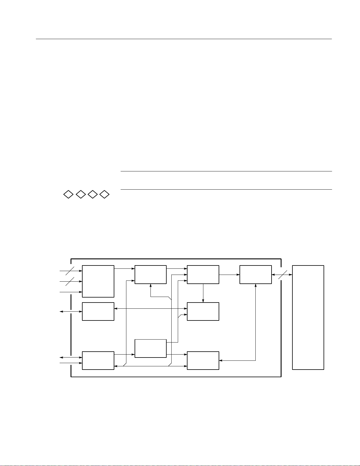
This module overview describes the basic operation of each functional circuit
block as shown in Diagram
. Figure 5-2.
TDS 520B Mod CM Component Service Manual
1–1
Page 20

Theory of Operation
General
Input Signal Path
The TDS 520B Digitizing Oscilloscope is a portable two-channel instrument.
Each channel provides a calibrated vertical scale factor.
A signal enters the oscilloscope through a probe connected to a BNC on the A10
Attenuator/Acquisition board.
Attenuators. Circuitry in the attenuator selects the input coupling, termination,
and the attenuation factor. The processor system, by way of the acquisition
system, controls the attenuators. For example, if 50 input termination is
selected and the input is overloaded, the processor system switches the input to
the 1 M position.
Probe Coding Interface. Probe coding interface signals pass through the attenuator
portion of the A10 Attenuator/Acquisition to the acquisition system, where they
are sensed and controlled.
Acquisition System. The acquisition system amplifies the input signals, samples
them, converts them to digital signals, and controls the acquisition process under
direction of the processor system. The acquisition system includes the trigger,
acquisition timing, and acquisition mode generation and control circuitry.
D1 Bus. The acquisition system passes the digital values representing the
acquired waveform through the A14 D1 Bus to the A11 DRAM Processor/Display board. This happens after a waveform acquisition is complete if the digital
signal processor in the processor system requests the waveform.
Processor System. The processor system contains a 68020 microprocessor that
controls the entire instrument. This system also includes the firmware and a
GPIB interface. You can reprogram the firmware from a remote controller using
the GPIB and an external software package.
The processor also includes a digital signal processor. This signal processor
processes each waveform as directed by the system processor. Waveforms and
any text to be displayed are passed on to the display system. The A11 DRAM
Processor/Display board contains both the processor and display systems.
Display System. Text and waveforms are processed by different parts of the
display circuitry. The display system sends the text and waveform information to
the tube assembly as a video signal. The display system also generates and sends
vertical (VSYNC) and horizontal (HSYNC) sync signals to the tube assembly. A
VGA-compatible video output is at the rear of the TDS 520B.
1–2
TDS 520B Mod CM Component Service Manual
Page 21

Theory of Operation
Tube Assembly
Front Panel
Rear Panel
All information (waveforms, text, graticules, and pictographs) is displayed by
the A20 Display system. The A20 generates the high voltages necessary to drive
the display tube. It also contains the video amplifier, horizontal oscillator, and
the vertical and horizontal yoke driver circuitry.
The processor system sends instructions to and receives information from the
Front Panel Processor on the A12 Front Panel board. The Front Panel Processor
reads the front-panel switches and potentiometers. Any changes in their settings
are reported to the processor system. The Front Panel Processor also turns the
LEDs on and off and generates the bell signal.
Front-panel menu switches are also read by the Front Panel Processor. The
processor sends any changes in menu selections to the processor system. The
ON/STBY switch is one of the menu switches. However, it is not read by the
Front Panel Processor, but passes through the A12 Front Panel board and the
A11 DRAM Processor/Display board to the low voltage power supply.
The front panel also generates the probe compensation signals SIGNAL
and GND.
The GPIB connector provides access to stored waveforms, and allows external
control of the oscilloscope. Other rear panel connectors are the AUX TRIGGER
INPUT, MAIN and DELAYED TRIGGER OUTPUT, and a CHANNEL 3
SIGNAL OUTPUT.
Low Voltage Power Supply
Fan
You can make hardcopies on the GPIB port. If your TDS 520B has the optional
RS-232 and Centronics ports, you can also use those.
The low voltage power supply is a switching power converter with active power
factor control. It supplies power to all of the circuitry in the oscilloscope.
The principal POWER switch, located on the rear panel, controls all power to
the oscilloscope including the Low Voltage Power Supply. The ON/STBY
switch, located on the front panel, also controls all of the power to the oscilloscope except for part of the circuitry in the Low Voltage Power Supply.
The power supply sends a power fail (~PF) warning to the processor system if
the power is going down.
The fan provides forced air cooling for the oscilloscope. It connects to +25 V
from the Low Voltage Power Supply by way of the A11 DRAM Processor/Display module.
TDS 520B Mod CM Component Service Manual
1–3
Page 22

Theory of Operation
1–4
TDS 520B Mod CM Component Service Manual
Page 23
Detailed Circuit Description
This detailed circuit description describes the operation of the oscilloscope
circuitry shown in schematic diagrams in the Diagrams section. While reading
this description, refer to the block diagrams and the schematic diagrams in the
Diagrams section.
Acquisition System A10
The A10 Acquisition board amplifies, via the attenuator assembly, and acquires
the analog signal. The acquisition system converts the signal to digital and stores
it in acquisition memory. Acquisition and trigger control circuitry controls the
acquisition process. DSP and the 68020 monitor and control the overall system,
and transfer the acquired waveform to the display system.
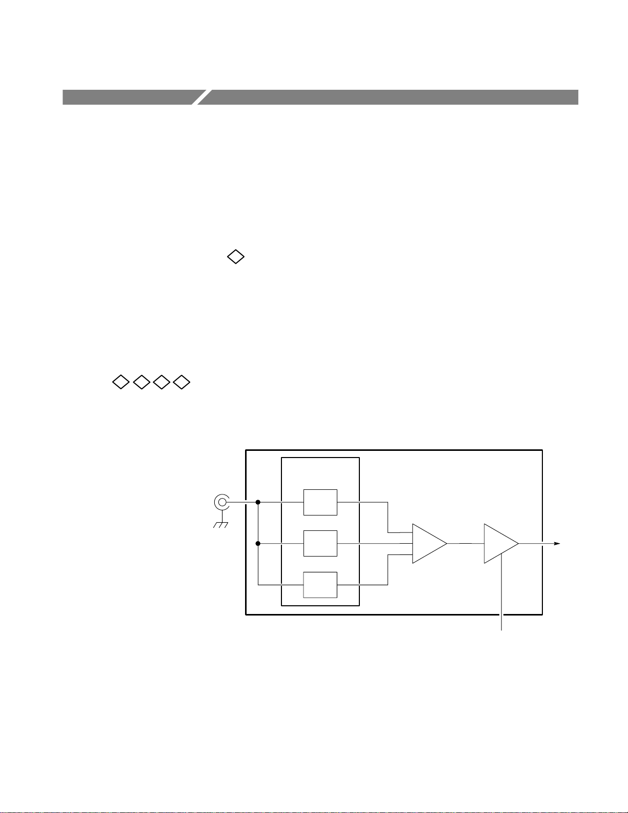
Attenuators A10
3
4 5 6
The attenuator assembly contains four attenuator hybrids, see Figure 1–1, and
four probe connectors. Each attenuator hybrid contains resistive dividers, an AC
coupling capacitor, relays, a 50 terminator, a buffer amplifier, and a preamp.
The outputs of the attenuator assembly (the preamp output) drive the track and
hold.
BNC
1
Resistive
dividers
1
Buffer Preamp
10
Figure 1–1: Attenuator hybrid
From here on the theory refers only to Ch4. The other channels work in similar
ways.
TDS 520B Mod CM Component Service Manual
100
Gain and
BW controls
1–5
Page 24

Detailed Circuit Description
Mode
The 68020 interprets user commands and initiates changes to the settings. The
Acquisition Processor monitors the input overload sense (OVLS1–OVLS4) and
the probe data (PRDATA1–PRDATA4) communication lines.
Each attenuator hybrid has five relays. One or more of the relays must be turned
on if a signal is to pass from the BNC to the output of the attenuator.
The AC/DC coupling relay couples the output of the BNC to the other relays in
the attenuator hybrid. For AC signals, the AC/DC coupling relay inserts a
coupling capacitor into the input signal path.
When active, the 1 M/50 relay terminates the input in 50 .
A relay driver (U1102, sheet 6) selects an attenuator’s attenuation factor by
connecting one of its relays to the input BNC, and connecting all of its other
relays to the ATTNCAL adjustment signal.
When ATTENSTB goes high, all attenuators enter their inactive state. Attenuator
clock CCATTN clocks control data (DIN, U1102, pin 3) from the processor
system into the attenuator Relay Driver. With a new pattern in the Relay Driver,
the processor system sets ATTENSTB low, enabling the attenuators.
The serial data line (DIN, U1102, pin 3) comes from sheet 21, U1050, pin 27.
The strobe (ATTENSTB, U1102, pin 8) comes from sheet 21, U1050 pin 11
(SCLK2). The DOUT line (U1102, pin 6) feeds the shifted data to the Ch3 relay
driver, where it becomes DIN for Ch3 (U1202, pin 3). This continues until Ch1.
After Ch1, the DOUT pin (sheet 3, U1402, pin 6) is sent back to sheet 21,
U1050, pin 6. By feeding the serial data back to the control IC (U1050), the
system can perform diagnostics on the serial data path.
T able 1–1: Relay Driver Control Data (CD) Bit Pattern
Bit
7 6 2 8 5 4 1 3
AC 1 NC
DC 0 NC
50 NC
1 M NC
1X BNC NC
10X BNC NC
100X BNC NC
1
1
1
1
1
1 NC
0 NC
NC
NC
NC
1
1
1
1
1
NC
NC
1
1
1
1
NC
NC
NC
NC
1
1
1
1
NC
NC
NC
NC
1
1
1
1
NC
NC
NC
NC
1
1
1
1
NC
NC
NC
NC
1
1
1
1
1 0 0 1 0 0
0 1 0 0 1 0
0 0 1 0 0 1
NC
NC
NC
NC
1
1
1
1
1–6
OFF 0 0 0 0 0 0 0 1
1XCAL NC
10XCAL NC
1
1
NC
NC
1
0 0 0 1 0 0
1
0 0 0 0 1 0
TDS 520B Mod CM Component Service Manual
Page 25
Detailed Circuit Description
T able 1–1: Relay Driver Control Data (CD) Bit Pattern (Cont.)
Bit
Mode
Mode 31458267
100XCAL NC
INACTIVE 0 0 0 0 0 0 0 0
1
NC equals no change.
1
NC
1
0 0 0 0 0 1
Preamps A10
3
4 5 6
Since the preamp circuitry for each preamp is similar, only the circuitry for
Preamp 4 is described. Preamp 4 provides gain switching, bandwidth limit
7
filters, and outputs for the display, trigger, and other signal paths.
The system processor controls the Preamp 4 functions. It sends commands over
serial data line.
The Analog DAC Control system provides DC voltage signals that set the
Preamp offset. The Acquisition Processor (U600) stores the digital values of
each of the voltage levels in digital-to-analog converter (DAC) U900. The
Acquisition Processor transfers each voltage through DAC Multiplexer U934 to
Preamp 4. Preamp variable gain, HF adjust, fine offset and balance controls are
controlled by the daculator (U904) which is controlled by the GTL (U1050) via
the serial data bus (SDOUT U1050).
Preamp 4 Control Buffers. (sheet 6) The Preamp 4 Control Buffers provide offset,
balance, variable gain, and high frequency compensation voltages for the
preamp.
The offset control voltage is sampled by U934 (sheet 26) and held on capacitor
C1101. U1405 buffers the hold voltage so it can be fed into the attenuator hybrid
and then to the preamp. Fine offset and balance controls do not need a hold cap
because they come from the daculator (U904) which internally holds the
voltages. Fine offset and balance are buffered by U1101 and then summed
together with offset. HF adjust and var gain are fed directly to the preamp from
the daculator (U904).
Preamp Control 4. U1403 and U1404 (sheet 7) are the serial in, parallel out shift
registers that load the preamp control bits. Serial data flows into U1403 pin 1
(from sheet 21, U1050, pin 27). The data is shifted into the registers by SCLK3
(U1403 and U1404, pin 8). SCLK3 comes from sheet 21, U1050, pin 12. Data
flows from the last bit of U1043 to the serial input pin of U1404 and then from
the last bit of U1404 back to sheet 21, U1050, pin 7 for diagnostic purposes.
There are three steps in the process of programming the preamps. First, 16 bits
are shifted into the two registers (U1403 and U1404) – only QA, QB, QC, QD,
and QE of each register will be used. The Ch1/Ch3 preamp strobe (sheet 3,
TDS 520B Mod CM Component Service Manual
1–7
Page 26

Detailed Circuit Description
JP1400, pin 112 and sheet 5, JP1200, pin 112) is strobed to latch the gain and
bandwidth bits into Ch1 and Ch3. This strobe pin comes from sheet 21, U1050,
pin 17. Next, 16 more bits are shifted in and again only the 10 bits mentioned
above are used. However, this time, the Ch2/Ch4 preamp strobe (sheet 4,
JP1400, pin 212 and sheet 6, JP1200, pin 212) is strobed to latch the gain and
bandwidth bits into Ch2 and Ch4. Finally, 16 more data bits are shifted in. These
are left there to set the output controls of all four channels.
Preamp 4. The preamps amplify the input voltage. Input signals come from the
attenuator. The nominal gain of each preamp is 1.05 (at 50 mV per division); the
gain of the attenuator is 0.95 (in 1X attenuation). The combined gain from BNC
connector to A/D Converter D is 1.00.
Preamp 4 is an integrated circuit containing:
H Two four-pole bandwidth-limit filters: 20 MHz and 250 MHz. Inputs B0–B1
control the bandwidth of Preamp 4. See Table 1–2.
H Six gain settings of 1 mV, 2 mV, 5 mV, 10 mV, 20 mV, and 50 mV per
division (see Table 1–3). Inputs G0–G2 control the gain of Preamp 4.
H High-frequency adjust inputs.
H A variable gain control input which linearly adjusts the overall gain. The
gain is zero at –1 V and maximum at +1 V.
H Three separate differential outputs that can be turned on or off using the
output enable control signals (out1en, out2en, out3en). The inv controls are
left at 0.
T able 1–2: Bandwidth Limit Selection Bits(Cont.)
Bandwidth B1 B0
20 MHz 0 0
250 MHz 0 1
Maximum 1 X
T able 1–3: Gain Set Bits
Gain Setting G2 G1 G0
1 mV 0 0 0
2 mV 0 0 1
5 mV 0 1 0
10 mV 0 1 1
1–8
TDS 520B Mod CM Component Service Manual
Page 27
T able 1–3: Gain Set Bits (Cont.)
Gain Setting G0G1G2
20 mV 1 0 X
50 mV 1 1 X
Detailed Circuit Description
Track/Hold A10
8
The track/hold IC (U1250) samples the differential analog signals coming from
the preamps before sending them to the A/D converters. The A/D clocks are also
provided by the track/hold. The track/hold IC also provides all channel switching
necessary to facilitate 2–way and 4–way interleaving. There are 8 control bits
that are serially shifted into U1251 and parallel fed to the track/hold. The data
line (SDATA, U1251 pin 1) comes from sheet 21, U1050, pin 27. The data is fed
back (SDIAG1, U1251, pin 13) to U1050, pin 5 for diagnostic purposes). The
data is clocked in by U1251, pin 8 (which comes from sheet 21, U1050 pin 10.)
The differential analog signals coming from the preamps are labelled
DISP1+/DISP1– thru DISP4+/DISP4–. The differential clocks going to the A/D
converters are labelled CLKAH/CLKAL thru CLKDH/CLKDI. The differential
analog sampled signals going to the A/D converters are labelled AP+/AP–
through DP+/DP–. Note, from the top level block diagram, that the signals going
from the preamps to the A/D converters get crossed (see Tables 1–4, 1–5, and
1–6 to verify this).
T able 1–4: Preamps to Track/Hold Input
Track/Hold
Preamps
Ch1 DISP1
Ch2 DISP2
Ch3 DISP4 Ch3 and Ch4 cross here
Ch4 DISP3
Input
Comments
T able 1–5: Track/Hold Outputs to A/D Input
Track/Hold
Outputs
AP SIGB AP and BP cross here
BP SIGA
CP SIGC CP and DP are inactive on
DP SIGD
A/D Input Comments
TDS 520B Mod CM Component Service Manual
the TDS 520B and
TDS 724A
1–9
Page 28
Detailed Circuit Description
T able 1–6: Preamps to Track/Hold Input
Track/Hold
Clock
Outputs
CLKA CLKB
CLKB CLKA
CLKC CLKC CLKC and CLKD are inactive
CLKD CLKD
A/D Clock
Input
Comments
on the TDS 520B and
TDS 724A
In order to provide interleave capability, the Track/Hold must independently
adjust the delays of each of the sample clocks going to the A/D converters. These
are controlled by PHSA, PHSB, PHSC, and PHSD (pins 10, 111, 31, and 90
respectively of U1250) analog control voltages from the daculator (sheet 24,
U906). A three phase version of the 1GHz timebase clock is fed in through the
PHS1, PHS2, and PHS3 signals.
A/D Converters A10
1211109
NOTE. The TDS 520B and 724A only have A/D converts A and B. C and D are
not placed.
Since each A/D converter is similar, only the circuitry for A/D Converter D is
described. A/D Converter D (U700) converts the selected differential analog
input voltage to an 8-bit binary number. The analog input sensitivity is 2 mV per
digitizing level. Conversions occur at the 1 GHz clock rate (CLKD U700, pins
53 and 55). Even though conversions occur at this rate, data is output as two
differential 8-bit words (D0H/D0L–D7H/D7L and A0H/A0L–A7H/A7L) at a
500 MHz rate.
Pipes C and D (sheets 11 and 12) are not placed in the TDS 520B and TDS
724A.
Inputs. The A/D converter has one differential input (pins 60 and 62) fed from
the track/hold. Tables 1–4, 1–5, and 1–6 show which track/hold output connects
to which A/D converter. The 1 GHz differential input clocks from the track/hold
are fed into pins 53 and 55. Each side of the differential clock is 250 mV p–p
swing with the high level at 0 V.
Outputs. Outputs from the A/D Converter are differential, 500 mV digital swings
(peak to peak on each side.) The output resistance is 65 ohms. The two 8–bit 500
1–10
TDS 520B Mod CM Component Service Manual
Page 29
Detailed Circuit Description
MS/s streams become valid on alternate edges of the clock cycle (D is valid on
the rising edge, A is valid on the falling edge.)
Control. The A/D converter has two DC analog controls: OFFSET, which sets the
A/D offset, and VREF, which adjusts the gain. These controls come from a
daculator IC (U906, sheet 24). The VREF control voltage is preconditioned by
U701 so that it ranges from 1.56 V to 3.44 V.
Sampling of the analog input voltage occurs on the positive going transition of
convert clock (CLK0, pins 53 and 55). Digitized value is available after the 11th
subsequent clock cycle.
DMUX & Acquisition
Memory A10
ADATA_D
DDATA_D
ADCLK_D
8
8
16151413
Level shift
Trigger
interface
NOTE. The TDS 520B and 724A only have pipes A and B placed. They do not use
C and D.
Since the circuitry for each demultiplexer and acquisition memory is similar,
only the circuitry for pipe D Acquisition Memory is described. The demultiplexer is the time base and memory control system for the output of an A/D
converter. Each demultiplexer has an A/D data input (Ch4D and Ch4A),
acquisition memory output, DSP bus interface, and a trigger interface (see
Figure 1–2).
Demultiplexer Level shiftDecimators
Counters
64
Acquisition
memory
Decode
TriStar
interface
Figure 1–2: Demultiplexer Block Diagram
TDS 520B Mod CM Component Service Manual
Formatter
1–11
Page 30

Detailed Circuit Description
Demultiplexer D. Demultiplexer D has two operating modes. In acquire mode,
Demultiplexer D (U100) collects data from an A/D converter and writes the data
into Acquisition Memory D. In save mode, the DSP reads the acquired data from
Acquisition Memory D. The display system then processes and displays the data.
In acquire mode, Demultiplexer D (U100) gets its data (ADATA_DH0/ADATA_DL0 – ADATA_DH7/ADATA_DL7 and DDATA_DH0/DDATA_DL0 –
DDATA_DH7/DDATA_DL7) from A/D Converter D (U700) at a rate of two
new 8-bit samples every 2 ns. The input data sample is a 500 mV swing with
Von 4.2V. It latches the data on the falling edge of clock ADCLK_D and
converts it to CMOS levels. Data then passes to a demultiplexer at full speed, or
is decimated under program control.
The decimation mode determines the sample-rate. When the digital trigger is the
source of the trigger, the state of the decimators is latched at the trigger to assist
in point placement.
There are three decimation modes: normal, min/max, and hires:
H Normal (sub-sample) mode throws away samples between saved sample
points.
H Min/max mode saves the maximum and minimum samples over the
decimation interval.
H Hires mode gives extra resolution by averaging the samples, on a single-shot
basis, over the decimation interval.
An internal demultiplexer splits the two 8-bit data streams coming out of the
decimators into 16 8-bit data streams. The data streams are 2–way interleaved
resulting in a 64–bit data bus, with two memory chips on each byte. This results
in a 64-bit wide data word.
Demultiplexer D has three programmable counters that keep track of the number
of samples before the trigger, the number of samples after the trigger, and the
location in Acquisition Memory D where the trigger occurred. Before a trigger
occurs, the RUNM signal is asserted by the trigger logic (U1001, pin 146, sheet
20). After the trigger when the proper number of post–trigger samples have been
taken, RUNM is deasserted which stops the DMUX and causes it to interrupt the
processor.
During save mode, the DSP can access Acquisition Memory D. Memory mapped
I/O select MMIO accesses pin 74, the internal programming and status registers.
To further decode the MMIO select, the middle address bits are used as
sub-system selects.
1–12
Input MMIOA (U100, pin 73) acts as the sub-system selector for the memory
mapped I/O in the demultiplexers. To address the internal registers, DSP asserts
both MMIO and MMIOA.
TDS 520B Mod CM Component Service Manual
Page 31

Detailed Circuit Description
During DSP writes to Acquisition Memory D, circuitry in Demultiplexer D
aligns the byte-wide data for byte writes into Acquisition Memory D.
DSP can clock Demultiplexer D for test purposes. Diagnostics can switch in a
counter instead of A/D Converter D so that Demultiplexer D acquires a
predictable pseudorandom sequence.
Acquisition Memory D. During acquire mode, Demultiplexer D writes to
Acquisition Memory D when eight samples accumulate. The full 64 bits are
always written in parallel. Two address buses allow two sets of memory to share
the 64-bit data bus on alternate 8ns cycles.
Phase lock loop/clock
generator A10
17
Analog Triggers A10
18
The 1 GHz system timebase is generated from a VCO (centered around Q531)
that is phase locked to a 25 ppm, 25 MHz reference crystal oscillator. U510 is
the phase/frequency detector. The integrator is made from U502 and surrounding
components. The single–ended 1 GHz VCO output is converted to differential
(via delay lines) and fed to the trigger logic (U1001, sheet 20, pins 140 and 142).
The trigger logic divides the clock down to 25 MHz and feeds it back to the PLL
(from U1001, pins 12 and 13).
The analog triggers are free-running analog comparators with channel switching.
The following is described in terms of the Ch1 and Ch2 analog triggers:
The analog trigger comparator (U1551, sheet 18) is a channel switch and analog
comparator combination. Ch1 is differentially fed into IN1(H/L) (pin 5,4), CH2
is fed into IN2(H/L) (pin 41,41). The main trigger output is OUT11(H/L) (pins
20, 21) and the delay trigger output is OUT21(H/L) (pins 26, 25). The channel
switch allows either Ch1 or Ch2 to be the main or delay trigger event or both.
The comparators are after the channel switch, so the trigger level and hysteresis
controls are associated with the main delay trigger rather than Ch1 or Ch2
trigger. Trigger coupling is generated with U1560/U1561 filter circuits. Referring
to Ch1, AC coupled trigger occurs when C1556 is connected to ground via
U1556 and the analog trigger (U1551) is programmed to subtract this filter
output from the Ch1 trigger input signal. LF reject is achieved similarly except
C1556 is disconnected from ground. HF reject is like LF reject except that rather
than subtracting the CP1 input signal (pin 7) from the Ch1 trigger signal, the
CP1 input signal itself is used as the input. Noise reject is done by increasing the
trigger hysteresis via those analog control voltages (pins 11 and 35 for main and
delay hysteresis respectively).
U1552 does the same thing for Ch3 and Ch4. The EVNT1–4 outputs from
U1551 and U1552 are fed to the trigger logic IC (U1001, sheet 20), The trigger
logic chooses between Ch1/2 and Ch3/4 for main and delay trigger events.
U1551 and U1552 contain built–in shift registers for programming of the
channel switch and coupling modes. The serial data SDATA comes from U1050,
TDS 520B Mod CM Component Service Manual
1–13
Page 32

Detailed Circuit Description
sheet 21, pin 27. The data is fed serially into U1551, then U1552, and then back
to U1050, pin 91. The data is clocked into the shift registers with SCLK0
(U1551/U1552, pin 13) from sheet 21, U1050, pin 92. Once the shift registers
are loaded, the data is latched in by strobing DSTR0 (U1551/1552, pin 33).
DSTRB0 comes from sheet 21, U1050, pin 93.
Trigger Logic A10
20 21
Extended Trigger A10
22
Trigger Logic is the digital part of the trigger system. It is composed of two IC’s
referred to as U1001 and U1050. The circuitry has many clock generation and
triggering functions:
H Divides the 1 GHz VCOH/VCOL by 4 to get 250 MHz. The 250 MHz is
used to drive the time interpolators. It is further divided to operate the trigger
logic. It is also divided by 10 to generate the 25 MHz used by the scope’s
timebase PLL.
H Provides proper timing on the two resets (ACQRST1 and ACQRST2).
H Selects the trigger event.
H Puts the oscilloscope into posttrigger mode when the trigger is detected.
H Places the trigger point with respect to the data in memory.
H Provides trigger measurement functions.
H Provides part of the trigger holdoff and time interpolator functions.
The Extended Trigger (EXTL) is primarily used to trigger on the end of an event
pulse, qualified by the width of that pulse in time. Extended Trigger also allows
the trigger system to act as a flip-flop, as in state trigger.
1–14
The Extended Trigger responds to digital signals or “events” provided by the
Analog Triggers and the Trigger Logic. When a trigger condition is satisfied, the
Extended Trigger, (U1703, sheet 22) generates EEVNT.
A combination of analog ramps and the Trigger Logic define the reference pulse
widths. The analog ramps cover fast timing settings, while the Trigger Logic
counts pulse widths greater than 1 microsecond. For time references less than or
equal to this (where only the ramp is used), the Trigger Logic counter is disabled
and the outputs are set high.
Daculator-derived ramp currents at pins 10,11,12, 34, 35, and 36 define the
analog ramp times. The pins should always be within 25 mV of ground.
Each pulse width timer has two DAC/resistor networks. The slow range uses a
150 kW resistor for 30 ns to 1 ms. The fast range uses 4.75 kW for 2 ns to 28 ns.
TDS 520B Mod CM Component Service Manual
Page 33

Detailed Circuit Description
Time Interpolators A10
23
There are two time interpolators. One is for the main trigger, and the other is for
the delay trigger. The time interpolator allows the trigger system to determine the
time of occurence of a trigger event to the sub clock cycle resolution needed at
fast time/div settings.
A triple ramp technique is employed to perform the interpolation. When the
trigger event occurs, a large current is injected onto a capacitor generating what
is called the fast ramp. When the second subsequent clock occurs, the fast
current stops and the capacitor has a voltage that is proportional to the amount of
time from the trigger event to the next clock cycle plus a fixed offset. After the
fast current shuts off, a medium current starts to discharge the capacitor
generating what is called the medium ramp. This drains off most of the fixed
offset. At the end of the medium ramp, the medium current shuts off and is
replaced by a small current which slowly discharges the capacitor generating the
slow ramp. The time taken by the slow ramp to finish discharging the capacitor
is proportional to the initial time interval between the trigger event and following
clock edge. This system measures this much slower slow ramp time to obtain the
measurement.
For the main time interpolator (U1600, sheet 23), the fast ramp is set by R1640
and R1641. The slow and medium ramp currents are set by the control voltages
ISMAIN and IMMAIN respectively during SPC. The control voltages are
buffered by U1601 before being applied to the current setting resistors (R1639
and R1638).
Daculators A10
24
The trigger event is fed differentially into pins 10 and 11 of U1600 (MAUTH/L).
The differential clock is fed into pins 4 and 3 (TICLKMH/L). The timing ramps
are all internal to U1600 – an internal clock is generated that clocks a five-bit
counter for the duration of the slow timing ramp. The MSB of this counter
(CNTENMP/N, pins 44, 43 of U1600) is fed to U1050, sheet 21 where it clocks
a larger counter in that chip thus effectively concatenating the two counters to
make one counter. When the clock in U1600 stops, the counter is left with a
number proportional to the time from the trigger event to the next clock edge.
Once the system stores the trigger measurement, the trigger event line MAUT/L
is set low which resets the time interpolator.
The time interpolator also synchronizes the trigger event (U1600, pins 28, 27)
and returns it to U1001, sheet 20, pins 18 and 19. Operation for the delay time
interpolator is identical except it is in U1650, sheet 23 and operates on delay
trigger events.
Most of the analog control voltages are generated from the daculator ICs (U904,
U905, and U906). The daculators contain an internal 12–bit DAC, 1:16 analog
multiplexing circuit, and buffers. Serial data SDATA is shifted into the three
daculators (starting with U904) which are strung together daisy chain style. The
data serially shifts out of U906 (SDIAG4) back to U1050, sheet 21, pin 8.
SCLK4 clocks the serial shift registers (it comes from U1050, sheet 21, pin 14).
TDS 520B Mod CM Component Service Manual
1–15
Page 34

Detailed Circuit Description
DSTRB6 (from U1050, sheet 21, pin 25) causes the shifted data to take effect.
The data contains information on which daculator voltage to change and what
voltage to change it to. This is a total of 16 bits per daculator or 48 bits total.
Calibrator A10
25
Acq Processor A10
26
DAC and analog
MUXs A10
26
U962, U963, and U950 along with the supporting circuitry on that sheet form the
circuitry that generates the calibration voltages for Signal path Compensation
(SPC). U962 samples VDAC10 and stores that voltage on C956. VDAC10
comes from the DAC on sheet 26 (U900, pin 9). U963 selects an attenuated
version of this stored voltage for 1x, 10x, or 100x calibration. It can also select
ground for offset calibration. U962 and U963 are controlled from the trigger
logic (sheet 21, U1050, CVR0–6). The percent error of VDAC10 is characterized
at factory cal and stored along with all other calibration constants in NVRAM
(U1052 and U1055, sheet 21).
The system processor communicates commands to the Acquisition Processor
(U600) via the D1 Bus. The Acquisition Processor in turn controls the acquisition process. It controls the DAC and analog multiplexers that send control
voltages to the preamps. The Acquisition Processor also controls the probe
interface and senses internal temperature and timebase PLL lock.
U900 is a 12-bit DAC that is controlled by the acquisition processor. The analog
MUX (U934) stores the DAC output on hold capacitors. As the acquisition
processor changes the DAC output through a sequence of output voltages, the
analog multiplexor switches in sync with the DAC to store each voltage on a
different hold cap. There are 8 hold caps connected to U934 – four of them
(C939 C942) control probe offset, the other four (C1401, C1301, C1201, C1101
on sheets 3, 4, 5, and 6 respectively) control offset to the preamps. The output of
the DAC is reduced by a factor of four to ±2.5 V before being fed to U934. The
full ±10 V output of the DAC is also fed to U962 in the calibrator system on
sheet 25 where its held value is used for calibration voltage generation. The
acquisition processor controls the cycling of both the DAC and the analog MUX.
1–16
TDS 520B Mod CM Component Service Manual
Page 35

Detailed Circuit Description
Processor System A11
The processor system includes two processors: the 68020 (U1155) and U1097
the Digital Signal Processor (TriStar). The 68020 processor coordinates all
oscilloscope activities. It also directs the activities of the Acquisition Processor
and the Front Panel Processor via a parallel to serial interface using DUART
U1317. The Digital Signal Processor (DSP) manipulates acquisitions. It
performs tasks as directed by the 68020 processor and reports results back either
through interrupts or by using the FIFO (U1074). The 68020 has access to
everything on the DSP bus, allowing it to run diagnostics, retrieve waveforms,
pass data, and load DSP instruction memory.
Processor/Display Board
Connectors A11
2 3
Decode A11
4 5
All connectors for the A11 DRAM Processor/Display board are grouped together
on these schematics. Regulator U12 supplies power for the NVRAM write
enable circuitry. Connector J20 connects power to the fan.
The Decode circuitry decodes the 68020 memory space (U1055, U1056),
generates wait states, data transfer and size acknowledge signals U2001, byte
enables U2001, and the system ON/STBY signal.
Main Decode. The Main Decode. circuitry decodes the 68020 address space into
16 blocks of 16 Megabytes each. Table 1–7 shows the memory map for the
Processor System.
1
68020 Interrupts, Kernel
Registers, and
Decode A11
5
Wait State
. Dynamic bus sizing allows the 68020 to automatically determine
5
the size of a port on each access by using DSACK signals.
Wait states are generated either from the device or port being accessed.
Data transfer and size acknowledge signals ~DSACK0 and ~DSACK1 control
bus speed (by adding wait states) and dynamic bus sizing for circuitry that does
not generate its own data transfer and size acknowledge signals.
Byte Enable Decode
. Byte Enable Decoder prevents the 68020 from
5
overwriting data during writes to word and long-word ports.
The 68020 supports seven levels of auto-vectored interrupts. Level seven
auto-vector (non-maskable) interrupts are reserved for ~PF, an interrupt
indicating that power failure is imminent, and ~50OHMOVERLOAD, an
interrupt indicating an overload in the A15 Attenuator. Interrupts from other
modules are shared on the other 6 interrupt levels. Table 1–21 lists the device
assigned to each interrupt level, and the name of the interrupt signals.
TDS 520B Mod CM Component Service Manual
1–17
Page 36

Detailed Circuit Description
Interrupt Decode. Interrupt circuitry in U2000 decodes interrupts into the three
signals that notify the 68020 of an interrupt. The ENABLEINT from the Bus
Control Register in U2000 determines if only level seven and Kernel interrupts
are enabled, or if all interrupts are enabled. Because the Interrupt Read Registers
are outside the Kernel, in Kernel operation the 68020 must read from the
interrupting device itself to determine the source of the interrupt.
Interrupt Mask and Miscellaneous Registers. All interrupts other than level 7 are
maskable. By asserting the appropriate mask bit in the Interrupt Mask register
(see Table 1–22) for an interrupt, the 68020 can ignore that interrupt. The 68020
can still read the status of the interrupt using Interrupt Read Registers.
The 68020 processor writes to Miscellaneous Register to control system circuitry
and one interrupt mask (see Table 1–22). By reading Miscellaneous Registers,
the 68020 processor determines the status of the interrupt masks.
Clock Logic. Clock logic uses a 25 MHz clock to generate clocks for buss error
logic, GPIB, DUART.
Kernel CPU and
Control A11
5 6
DRAM Logic. DRAM logic generate address and control signals for DRAM.
Interrupt Read Registers. Since there is usually more than one interrupt per
priority level, the 68020 processor reads the Interrupt Read Registers to
determine which device caused the interrupt (see Tables 1–24 and 1–25).
At the start of power-up, the 68020 (U1155) disables as many subsystem buffers
as possible. This allows the 68020 processor to start execution with as small a
system as possible (the Kernel). As diagnostics progress, subsystems are turned
on and diagnosed one at a time.
CPU and Control. After the Kernel passes its power-up diagnostics, the firmware
enables the control bus buffer U1135. Gates U1001C, U1082B, and U1082D
generate the DSP read and write control signals ~ERDS and ~EWRS.
U2001
combine all data transfer and size acknowledge signals (DSACKs)
5
from circuitry throughout the system, and generate the actual data transfer and
size acknowledge signals.
Kernel Address Decode and Kernel Wait States
. To isolate the Kernel from the
5
rest of the system, the Kernel decodes its own address space using decoders
inside U2000. The DSACKS control bus speed and allow for dynamic bus sizing
(byte, word, or long word).
1–18
TDS 520B Mod CM Component Service Manual
Page 37

Detailed Circuit Description
Bus Control Register 5. The Bus Control Register contains system control bits.
They include interrupt mask and enable bits, main bus enables, power down
initiation, and other control bits.
Kernel Memory, IO and
Buffers A11
7
Bus Error Logic
. A “watchdog timer” inside U2001 of approximately 2
5
milliseconds monitors 68020 cycle times. If any cycle exceeds 2 milliseconds,
then it generates a bus error (~BERR). Bus error can also be asserted when the
68020 tries to write to the Boot ROM. .
Reset. The 68020 processor resets both at power-up and power-down using the
reset signal into U1155 pin C1. Reset controller U1175 controls system reset.
Power-on reset asserts for a minimum of 400 milliseconds after the +5 V supply
stabilizes. Power-off reset asserts when the supply falls below a usable threshold
or when the 68020 asserts PWRDWN.
Kernel resident memory, IO, and buffers allow diagnostics to run while isolated
from the rest of the oscilloscope.
Kernel RAM. Kernel RAM. (U1336) runs internal diagnostics and flash EPROM
burn routines. It can also run down-loaded diagnostics.
Boot ROM. The Boot ROM. contains the 68020 power-up instructions. The
instructions begin with diagnostics. In addition, the Boot ROM. has the software
for operating the GPIB and programming the system flash EPROMS.
Address Buffers and Data Buffers. These buffers isolate the kernel address and
data lines from the rest of the system. The Bus Control Register enables or
disables these buffers.
7 Segment LED. Power-up diagnostics use this seven segment LED to communicate the pass or fail status of kernel diagnostics.
DIP Switch
5
diagnostic or firmware routines to run.
GPIB. The circuitry is made up of GPIB controller U1305, with transceivers
U1302 and U1311 buffering signals to and from the GPIB.
ID Register
5
Processor/Display board type and revision number.
TDS 520B Mod CM Component Service Manual
. The 68020 reads this switch at power-up to determine which
. Two ID Registers inside U2000 determines the A11 DRAM
1–19
Page 38

Detailed Circuit Description
Memory A11
8
Clocks, FPP, ACQP, and
Display Interface A11
9
The Memory subsystem includes NVRAM for power-off storage and Dynamic
RAM for the main system RAM.
NVRAM. The NVRAM. consists of non-volatile memory IC. This RAM provides
long-term power-off storage of calibration constants, front-panel settings,
waveforms, and hardware write-protected calibration constants.
NVRAM Write Protect. NVRAM Write Protect. circuitry can prevent a write to
portions of the NVRAM. that are reserved for calibration constants.
DRAM. Dynamic RAM is organized as 512K long words of memory for a total of
2 Megabyte. The circuitry includes the DRAM ICs, a dynamic RAM controller/
driver U2001.
DRAM Controller
. DRAM Controller automatically refreshes the DRAM..
5
During a normal 68020 access the dynamic RAM controller multiplexes the
address (on A2 to A21) onto the UMA0 to UMA8 address lines.
Clocks for the Processor System and the Display System are shared and are
derived from 25 MHz and 32 MHz oscillators Y1, Y2. The clock circuitry
divides the 25MHz_OSC signal by varying amounts to produce the clocks
needed by oscilloscope circuitry.
The Bus Control Register buffers and enables the Clocks, FPP, ACQP, and
Display Interface subsystem prior to 68020 access. Devices on the Clocks, FPP,
ACQP, and Display Interface subsystem (SP bus) are the DUART and the 68020
port into the Display system.
SP Data Buffers. The SP Data Buffers. buffer the main system data bus (D16 to
D31) to the SP data bus (SPD16 to SPD31).
Clocks. Y1 (25 MHz), and Y2 (32 MHz) crystal oscillators generate required
clocks for processor and display circuits.
DUART (Front Panel and Acquisition Processor Interface). The DUART (U1317) is
the 68020’s parallel-to-serial interface for both the Front Panel Processor and the
Acquisition Processor.
Table 1–19 lists the serial port interface signals to both the Front Panel Processor
and the Acquisition Processor.
1–20
TDS 520B Mod CM Component Service Manual
Page 39

Detailed Circuit Description
68020 to DSP Buffers and
Latches A11
10
DSP and Instruction
Memory A11
11
DSP D1 Buffers, Latches
and Memory A11
12
DSP D2 Buffers, Latches
and Memory A11
13
The 68020 to DSP Buffers and Latches buffer the 68020 address and data buses
to the DSP address and data buses.
Digital Signal Processor U1097 (DSP) provides fast waveform processing. The
processor uses prefetched instructions, from DSP Instruction Memory, and two
data memories. DSP Instruction Memory is loaded at power-on by the 68020.
The memory is 24 bits wide, fetched twice per DSP cycle, for an effective 48-bit
instruction word.
Buffers U1084 and U1083B buffer the DSP’s read and write signals to its three
buses. When BUSGRANT goes high, the outputs enter their high impedance
state, so that the 68020 can use the DSP’s buses. Table 1–13 lists the memory
map for the DSP Memory.
In general, the acquisition system uses the D1 Memory. The buffers and latches
buffer and demultiplex the X bus from the DSP to create the D1 bus. When the
bus is granted to the 68020 (BUSGRANT is high), the outputs of the buffers and
latches enter their high impedance state.
In general, the display system uses the D2 Memory. The buffers and latches
buffer and demultiplex the Y bus from the DSP to create the D2 bus. When the
bus is granted to the 68020 (BUSGRANT is high), the outputs of the buffers and
latches enter their high-impedance state.
DSP Bus Arbitration
Interrupts D2MMIO and
FIFO A11
14
D2MMIO Decoding decodes the address space and generates chip selects for all
registers on the A11 DRAM Processor/Display board accessible by the DSP.
The DSP D2MMIO Misc Register inside U2111 controls 68020 interrupts and
tells both the DSP and the 68020 whether or not the FIFO is full. Table 1–14
describes the contents the D2MMIO Misc Register.
The DSP performs tasks as directed by the 68020 processor and reports results
back either through interrupts or by using the FIFO (U1074). The DSP can pass
data back to the 68020 through the FIFO without having to halt DSP processing.
Interrupt ~FIFOINT, to the 68020, is generated when any data is in the FIFO,
and ~FIFOFULL internal to U2111 tells the DSP not to write to it or data will be
lost.
DSP Bus Arbitration and
Interrupts A11
14
Many buses in the oscilloscope are accessed by more than one processor. The
bus arbitration circuitry inside U2111 ensures that only one processor at one time
may access a bus.
TDS 520B Mod CM Component Service Manual
1–21
Page 40

Detailed Circuit Description
Display System A11
Bus Arbitration. The 68020 has access to all of the DSP’s address space on the D1
Memory, the D2 Memory, and the DSP Instruction Memory buses (see Table
1–7, 68020 Memory Map).
DSP Interrupts. The DSP has only one interrupt level. The interrupt circuitry is
similar to the 68020 interrupt circuitry. Interrupt mask (see Table 1–11) and
status (see Table 1–12) registers allow the interrupt routine to determine which
device(s) have interrupts pending and allow the masking of each interrupt. Table
1–12 lists the interrupt signals.
The Display System drives a 60 Hz non-interlaced, raster-scan CRT.
The display circuit’s primary function is writing waveforms into a waveform
plane. The circuitry provides several different display modes. These modes
include the Vector (Raster), Dot, XY, and YT modes.
D2 Interface and Display
Control Register A11
14
There are four main blocks in the display circuit: the Pixel Processor, the Vector
Lists, the Address Counter, and the Rasterizer. These blocks are connected
together in different ways for different display modes.
The Display System is a graphics system with two bit maps: the text plane and
the waveform plane. All information displayed is first written to one of these two
planes. The information is sent at regular intervals to the RAMDAC, which
converts it into an analog video signal. The contents of the bit maps are modified
through two different paths. The waveform display circuit, which is on the DSP
D2 bus, normally modifies the waveform plane, and the 68020 modifies the text
plane. The Video System Controller. and Video Timing blocks inside U2100
generate signals which affect the display system.
To maximize the waveform update rate, only waveforms are written to the
waveform plane. All other displayable information such as the graticule, readout,
cursors, and menus is written to the text plane. Both planes may be updated at
the same time.
The waveform display circuit takes a list of sample points, translates them into
bit pattern, writes those bit pattern in the proper location, and interrupts the DSP
when it is done.
The DSP D2 Interface connects the Rasterizer, Pixel Processor, Vector Lists,
RAMDAC, Display Control Register, and part of the Video Timing to the DSP.
It also generates two interrupts and a wait signal to the DSP system.
1–22
Display Control Register inside U2111 is an 8-bit register whose data lines are
connected to D2D8–D2D15.
TDS 520B Mod CM Component Service Manual
Page 41

Detailed Circuit Description
Vector List 0 and Vlist
Address Counter A11
16
Vector List 1 A11
17
Rasterizer A11
18
A vector list stores waveform sample data. Before starting a normal display
mode, the DSP writes data to a vector list. After the DSP starts the Pixel
Processor, the Pixel Processor reads the waveform sample data from the vector
list.
The Pixel Processor controls the Vector List Address Counter which addresses
the vector lists during waveform display modes. It is an 11-bit counter (U28,
U29, U30) with three control lines: PIPEN, CLKOUT, and ~LINEND.
This circuitry performs the same function as Vector List 0.
The primary function of the Rasterizer is to “draw” vectors between sample
points. It also generates waveform display control signals.
To rasterize waveforms, the Rasterizer generates an intensity for every point in
the waveform plane. It generates points from left-to-right top-to-bottom, in the
same way a raster scan CRT scans the phosphor. The Rasterizer outputs the
intensities to the Pixel Processor on LV3–LV6.
Rasterizer U59 has internal registers and lookup tables that the DSP can access.
During internal accesses the Rasterizer uses address inputs D2A0-D2A8 to
determine which register or memory is being accessed. Signal ~VFVIEN is low
during an internal access.
Pixel Processor and
020/WFM Data
Buffers A11
19
The PP Data Buffers and the 020/WFM Data Buffers buffer and multiplex the
Pixel Processor data bus onto both the 68020 data bus and the SP data bus. The
PP Address Mux’s multiplex the DSP D2 address bus and the vector lists data
outputs onto the Pixel Processor address bus.
Like the Rasterizer, Pixel Processor U60 has both internal registers and lookup
tables that can be accessed from the DSP.
The DSP D2 Interface asserts ~MEMACC or ~INTACCP during accesses to
internal registers. The Pixel Processor asserts WAITP whenever it is in a display
cycle. A DSP access to Pixel Processor address space with WAITP asserted
causes a XWAIT (U2111 pin 37) signal to the DSP.
Pixel Processor U60 contains the display circuit state machine, the control
interface to the waveform planes, and hardware for implementing many of the
display modes. The display modes are selected from a register inside the Pixel
Processor.
A memory refresh or display update cycle forces the current display mode to be
temporarily suspended.
TDS 520B Mod CM Component Service Manual
1–23
Page 42

Detailed Circuit Description
For each display mode, except system processor access mode, the following
steps are taken to start the Pixel Processor state machine:
1. Select the desired mode.
2. Write to the X register.
3. Write to the Y register.
The Pixel Processor then asserts WAITP and starts the desired mode. When
finished, the Pixel Processor deasserts WAITP and asserts ~DISPINTTS, which
interrupts the DSP. (Random dot mode does not generate a ~DISPINTTS
interrupt.)
Waveform plane refresh cycles and 68020 access occur through the Pixel
Processor.
The Pixel Processor also performs the top and bottom clip display functions on
waveforms.
H Top Clip will not display points whose vertical coordinate is above the value
stored in the Pixel Processor’s top register. A vertical coordinate of 0 is
considered the top of the screen.
Waveform Plane
0 and 1 A11
20
H Bottom Clip will not display points whose vertical coordinate is below the
value stored in the Pixel Processor’s bottom register.
The waveform planes are 512 by 512 bit maps. Only the upper 480 lines are
displayed.
The Pixel Processor has exclusive control of all waveform plane control lines
with two exceptions:
H The Video System Controller. can access the waveform planes during control
cycles such as DRAM. refresh cycles.
H The 68020 can access the plane in diagnostic mode.
Either the Pixel Processor or the 68020 can supply the data for the waveform
plane.
In system processor access mode, VRAM control signals from the Video System
Controller. (U2100) control the waveform plane control lines through the Pixel
Processor.
WFM Address Multiplexers. The WFM Address Multiplexers. multiplex the
VSC’s VRAM address lines, VA0–VA7, to the waveform planes address inputs
when ~VADEN is low. ~VADEN goes low only if the SPACC bit in the
Rasterizer mode register is high.
1–24
TDS 520B Mod CM Component Service Manual
Page 43

Detailed Circuit Description
The 020/WFM Data Buffers allow 68020 data onto the waveform plane data bus.
Waveform 0, 1 Memory. Waveform 0, 1 Memory. stores the actual waveform data
that will be displayed.
Text Planes and
Display A11
21
The Video System Controller. refreshes the text and waveform planes and
generates video control signals. The 020/VSC Interface. controls communication with the Video System Controller..
020/VSC Interface. The major functions of the 020/VSC Interface. inside U2100
are to communicate with the Video System Controller. and the 68020 (during
68020 accesses to the display). This interface circuitry also generates control
signals ~VADEN and ~WBFEN for 68020 access to the waveform plane.
020/VSC interface determines whether the Video System Controller. can execute
a 68020 requested cycle. If not, it waits until the Video System Controller. is
ready and then tells it to start.
Video System Controller . Both the text plane and the waveform plane are made up
of dynamic VRAMs. Video System Controller. inside U2100 refreshes both of
these memory planes in one refresh cycle. The Video System Controller.
executes one DRAM refresh cycle for every scan line (every 31.25 ms).
The Video System Controller. also generates 3 video control signals, vertical
sync (~VSYNC ), horizontal sync (~HSYNC ), and blank (~BLANK). Horizontal and vertical sync are sent to the A20 CRT Driver along with VIDEO_OUT.
Blank signal ~BLANK blanks the VIDEO_OUT signal during vertical and
horizontal retrace periods.
A display update cycle runs once for every horizontal blanking interval. During
the cycle, the Video System Controller. transfers one row from both the text and
the waveform plane memories (VRAMs) to shift registers located inside the
VRAMs. Once the data is in the shift registers it is shifted out of the VRAMs
serially, thereby leaving the VRAMs’ random access port free.
Video System Controller. internal registers control how often, on what rows, and
at what points the Video System Controller. executes display update cycles.
T ext Planes. Text Planes 0, 1, 2, 3 store all non-waveform data. Circuit operation
resembles that of waveform plane 0. The text planes do not need an address
multiplexer because, with the exception of the Video System Controller., the
68020 has exclusive access to the text planes. The Video System Controller.
accesses the text plane only on control cycles such as DRAM refresh cycles.
Each text plane is a 1024 512 bit map with one bit per pixel. The upper
left-hand corner of the bit map, a 640 480 section, is sent to the RAMDAC.
TDS 520B Mod CM Component Service Manual
1–25
Page 44

Detailed Circuit Description
VGA RAMDAC
22
Color RAM DAC and
Frame Buffers A11
23
Video Timing, Save on
Delta and Color Interface
A11
24
The VGA RAMDAC (U199) converts the VGA signals from U2011 into 3
analog video signals, red, green, and blue. The RAMDAC and its internal
registers and memory are addressed from Dsp D2 memory space.
Video data and ~Blankout are latched into the RAMDAC on the rising edge of
25 MHz. The RAMDAC sets the VIDEO_OUT signal levels to 0 Volts upon
receiving ~Blankout.
The Color RAMDAC (U193) receives digital video signals from frame buffers
and convert them into an analog video signal. The Color RAMDAC and its
internal registers and memory are addressed from DSP D2 memory space.
Video data, (FS0–FS19) presented at the inputs are latched at the rising edge of
SCLK (20 MHz). VCLK is used to clock and synchronize ~LCS_BLANK. The
RAMDAC sets the VIDEO_OUT signal level to 0 volts upon receiving
~BLANKOUT.
Video Timing. The Video Timing circuitry inside U2011 generates control and
timing signals used throughout the display system.
Save On Delta. Save On Delta. and the Pixel Processor recognize that a trigger
has occurred. When it occurs, the DSP reads WFM_SAVE in the D2MMIO Misc
Register. Once WFM_SAVE has been activated, it remains active until cleared
by ~MEMACC.
Color Interface. 16 bits of waveform data and 8 bits of text data are multiplexed
inside U2101 to generate 5 bits of VGA data. U2011 converts these data to 24
bits of information for frame buffers.
1–26
TDS 520B Mod CM Component Service Manual
Page 45

Firmface A11
Detailed Circuit Description
Firmface section holds the Flash ROM, and allows 4 Meg of space for software
code.
Flash ROM Buffers,
Decoding, and Version ID
Flash ROM A11
27
This circuitry contains address and data buffers, address decoding, and Flash
ROM version identification circuitry.
The oscilloscope makes use of flash memories for its Flash ROM. This allows
the Flash ROM to be programmed while it is in the oscilloscope. With +12 V
supplied to the Firmface, the Flash ROM can be programmed via programs
running in Kernel RAM. , programs which are downloaded via the GPIB.
Flash Fundamentals. Programming Flash ROM involves three steps. In step one,
if the Flash ROM is not fully erased (erased byte = $FF), then it is programmed
to the zero-state. In step two, if step one was necessary, every cell is erased to the
one-state. Step three sequentially programs each long word with the desired data.
Only those cells that are zero bits are programmed. Bits that are ones are simply
left alone, in the erase state.
Writes to the Flash ROM are possible only when +12 V is supplied. The A11
DRAM Processor/Display board has a switch (S1002) that turns this programming voltage on and off. Switch forward = programming voltage on. This switch
should only be toggled forward or back as directed by the firmware update
program.
The program queries the A11 DRAM Processor/Display board and the Firmface
board for their ID numbers, so it can determine how to configure registers on the
A11 DRAM Processor/Display board and how to program the DRAM Controller
to enable the DRAM..
Front Panel A12
The front panel is the operator’s interface for controlling the user-selectable
scope functions. All front panel controls are “soft” controls in that they are not
connected directly into the signal path.
Pots and FPP A12
TDS 520B Mod CM Component Service Manual
The Front Panel Processor monitors the front-panel controls. It consists of a
single-chip microprocessor with built-in RAM, ROM, A-to-D converter (for
1
digitizing the potentiometer wiper voltages), a programmable timer (for
generating the outputs for the bell and probe compensator signal), and a serial
communications interface (for data transfer to and from the 68020).
1–27
Page 46

Detailed Circuit Description
The knob scanning circuitry, working with the A-to-D converter internal to the
Front Panel Processor, produces digital values for the wiper voltages of the front
panel knobs. Analog multiplexers U8 and U9 select one of 12 possible pot inputs
to read. Although there are only six knobs on the front panel, each is a continuous-rotation potentiometer made up of two wipers, separated by 180 degrees,
which contact a single resistive arc.
Three control lines to multiplexers U8 and U9 select the pot input or wiper
voltage to be read. The analog voltage at the wiper of the pot selected is applied
to the Front Panel Processor. This voltage is digitized, and the amount and
direction of change from the previously stored value is calculated. The change
information is sent to the 68020.
Switches A12
2
LEDS A12
3
Bell, Calibrator, and Power
Supply A12
4
The Front Panel Switches and Menu Switches are arranged in an array of eight
rows and columns. When a switch is closed, one row line is connected to one
column line through an isolation diode. A complete scan of the Front Panel
Switches consists of setting all eight row lines low, in sequence, and performing
an eight-column scan to check for a change from the state stored in the Front
Panel Processor. Low bits in the column-line data tell the Front Panel Processor
that a switch is closed.
The LEDs (light-emitting diodes) are arranged in groups of eight. They are
connected between the emitters of PNP transistors and a pull-up resistor to VCC.
The base inputs of the PNPs are connected to the outputs of 8-bit LED latches
U5, U6, and U7. The PNPs provide adequate electrical current, so that the LEDs
are bright enough. When the 68020 needs to turn a particular LED on or off, it
sends a command to the FPP indicating what to do to the LED, and which one to
change. The FPP converts the LED identification number to the LED address
within one of the three latches (U5, U6, or U7).
The Bell circuit gates an oscillating signal through output speaker LS1. As long
as Q of U3A (U3 pin 6) is low, transistors Q2, Q4, Q5, and Q6 are off, and
current is cut off to speaker LS1. When the Q output of U3A is high, LS1
produces a tone.
1–28
Flip-flop U3B of the Probe Compensator divides the 2 kHz signal from TCMP1
(U1 pin 2) by 2. Therefore, CALCLK is a 1 kHz square wave. When Q1 is on,
CALSIG is a positive voltage (approximately 500 mV). When Q1 is off,
CALSIG is at ground.
TDS 520B Mod CM Component Service Manual
Page 47

D1 Bus D14
The A14 D1 Bus board connects the DSP D1 Bus from the A11 DRAM
Processor/Display board to other boards in the instrument.
Low Voltage Power Supply A16
The low voltage power supply generates voltages used throughout the oscilloscope. It is a switching power converter with active power factor control.
Detailed Circuit Description
Primay Power Stages,
Load Channel Regulators,
Mains Trigger Filter A17
1
2 3
The AC Input includes an EMI filter (C5–C7, C11, L2, L3, and L7) and bleeder
resistor. Also, thermistors and varistors protect against excessive current (RT1),
voltage (RV1), and temperature (RT7).
The Standby Supply is a flyback converter. When an integral transistor in U12 is
on, the voltage on C12 is applied to T7. This voltage (at C22) is monitored to
provide the power fail warning signal ~PF (W4 pin 1).
The Boost Converter provides a pre-regulated bulk supply for the Main
Converter. Two parallel FETs (Q5 and 6) form the boost converter switch. When
pulsed on, energy is stored in boost inductor L1. When the FETs turn off, the
inductor energy is delivered to bulk cap C12. The U10 Power Factor Control
controls the on-time of the FETs to regulate the bulk voltage. The control circuit
also provides for near unity power factor at the mains input.
The PWM Control (A18
) references the secondary of T6 (+5.1 V
1
FEED BACK). It turns Main Converter switching FETs Q7 and Q8
(A17
) on and off by way of gate drive transformer T4. With Q7 and Q8 on,
1
the bulk cap voltage is applied to the primary winding of transformer T6.
The Pulse Width Modulator (A18
) width-regulates the GATE DRIVE pulse
1
(Q10/Q11 base) regulating the main output voltage (+5.1 V).
The +24 output voltage is regulated from +5.1 through T6 turns ratio. The other
four outputs are series pass regulated by VR10, VR11, Q14, and Q15. An output
voltage summing comparator (U5) starts hiccup mode if one of these four
outputs go outside of the 50% voltage window.
PWM Control ,
Fault Signal
Conditioning A18
1
Pulse Width Modulator U5 is the heart of the PWM Control . Resistor R20 and
capacitor C4 set the switching frequency. R41, VR3, and C15 provide a 1%
reference. Capacitor C5 is a soft-start capacitor that slowly starts up the Boost
Converter.
2
Pin 10 of U5 is a shutdown input, and it is also a pulse-by-pulse current limit.
Pulling pin 10 high stops the output pulse within 200 ns. If pulled high for a
TDS 520B Mod CM Component Service Manual
1–29
Page 48

Detailed Circuit Description
short time, the soft-start cap (pin 8) will not be discharged. If the soft-start cap
discharges, it causes a normal soft-start when the voltage at pin 10 is removed.
Six signals are ORed together into the ONE-SHOT TRIG signal. They are the
24 V current limit, 24 V over voltage, the main 5.1 V over voltage, main 5.1 V
current limit, and the output voltage summing comparator. Any of these faults
will start hiccup mode. In hiccup mode the power supply cycles on and off at a
low repetition rate until the fault is removed.
The On/Standby Control debounces the switch. Relay K1 ensures that the power
supply powers up in the same state (On or Standby) it was in when the oscilloscope powered down.
The low bulk fault circuit monitors the bulk voltage by way of the peak detector
on the Standby Supply. It warns the processor system and shuts down the Main
Converter when the bulk voltage drops to about 300 V.
1–30
TDS 520B Mod CM Component Service Manual
Page 49

Display Driver Board A20
The TDS 520B uses a 640 × 480 pixel raster scan display. Scan rates are 60 Hz
frame rate × 32 kHz line rate.
Detailed Circuit Description
Display Block
Diagram A20
1
Inputs from
Display
Controller
24 V
V-sync
Video
20.S V
supply
Vertical
deflection
Trace
rotation
Blanking
amp
Video
amp
Focus
CRT
H-sync
Figure 1–3: Display block diagram
The display circuit board, CRT, and deflection yoke all form a basic raster
scanned picture monitor. Operating theory of this unit is very similar to most
such displays and the display portions of television receivers.
All inputs are made to the display through a 2 × 16 pin connector. The inputs
required are a video signal which produces the picture detail and horizontal and
TDS 520B Mod CM Component Service Manual
Horizontal
deflection
High
voltage
12 k
anode supply
1–31
Page 50

Detailed Circuit Description
vertical sync signals. The power for the display is provided by a single 24 volt
DC source at an operating current of about one amp. The video amplifier is DC
coupled and the signal must include a blanking pedestal to allow total extinction
of the CRT beam during retrace and to provide for good “black” level. Sync
signals are TTL compatible levels with the negative edge active.
The individual major sections are shown in the block diagram drawing. The CRT
beam is scanned in the X and Y axis by the Horizontal and Vertical deflection
circuits, which provide the scan currents for the deflection yoke. The “yoke” is
made up of the two sets of deflection coils and several fixed and adjustable
permanent magnets which allow for geometry correction and vertical and
horizontal positioning. This assembly is mounted on the CRT neck at the
transition to the funnel portion of the tube.
Several other calibration adjustments are provided to match the electronics to the
individual yoke and CRT characteristics. The Horizontal deflection circuit also
provides a large voltage pulse which is further increased by the high voltage
circuit to supply the 12 kV for the CRT anode and also to provide the other
internal supplies for the various circuits. CRT bias voltages for the CRT gun
elements and dynamic focus correction signals are developed in the block
marked “CRT Circuitry.” The Video Amplifier amplifies the video signal to
some 25–30 volts peak which them drives the CRT cathode to produce the Z axis
picture detail.
Display Block Diagram
Vertical Deflection
Circuit A20
1
The three-terminal regulator provides a stable supply for the scan circuits to
minimize changes in picture size due to any variations in the power input
voltage.
This circuit provides the scan current for the vertical (field) deflection coil. The
ramp of current moves the CRT beam from top to bottom of the CRT screen
during each field and returns to the top for the next field at approximately a
60 Hz rate. All of the active components are included in a single monolithic IC,
which is heat sunk to dissipate substantial power. Peak-to-peak currents of
between one and one half and two amps are needed to deflect the beam over the
required area. The output of the circuit is a current ramp, modified in shape to
correct for geometric error in the CRT and for deflection coil anomalities.
A negative pulse at the deflection rate is introduced to the sync input of the
circuit. This input may be either negative or positive; the sync circuit will
recognize either, and causes the ramp to “retrace” to the top of the screen. The
negative edge is the “active” edge in this application.
The retrace portion of the ramp signal occurs in relatively short time (less than
400 msec) and to overcome a rather large inductance of the deflection coil, a
“boost” voltage is applied to the output amplifier power supply rail. This larger
voltage allows the current in the yoke winding to change rapidly. Once the
retrace is complete, the supply rail returns to the normal voltage (21 V) to
conserve power in the output amplifier. At the same time, the Ramp generator
1–32
TDS 520B Mod CM Component Service Manual
Page 51

Detailed Circuit Description
portion of the IC has returned to the starting point of the ramp and will produce a
voltage ramp at the rate set by the R?C timing components until another sync
signal occurs. (in the absence of sync, the generator will reset itself at a
predetermined level and the scan will “free-run” at a slightly lower frequency).
An external component network modifies the ramp shape, resulting in a scan
waveform which will produce a “linear” movement of the CRT beam across the
face of the CRT. This correction causes the resulting ramp of voltage to acquire a
slight “S” shape, hence the majority of the correction is called “S” correction.
The center of the “S” may be moved about by the linearity adjustment to
accommodate non-uniformity of the deflection coil and other coil losses.
The modified ramp is fed to the input of the output amplifier. This voltage is
applied against a negative feedback signal which results from the deflection coil
current flowing in a small “current sampling” resistor. The output amplifier
signal is A–C coupled to the coil so that no D–C current will flow in the
windings. Such current would cause an undesirable “position” effect that would
vary with changes in the current. Some D–C voltage feedback is provided
directly from the amplifier output to stabilize the amplifier operating conditions.
An external compensation network insures the amplifier’s operating stability in
the presence of a highly reactive load and large amounts of negative feedback.
Horizontal Deflection
Circuit A20
1
The vertical size adjustment controls the amplitude of the ramp generator signal
and allows for precise vertical display size adjustment. Vertical positioning of the
rastered area is adjusted by movable permanent ring magnets mounted on the
back of the deflection yoke assembly.
The horizontal deflection signal is produced by applying a voltage across the
inductance of the deflection coil and allowing the current to build with time. At a
point in time the voltage is switched off and the retrace current is produced by a
resonant circuit which produces a large voltage across the inductance in the
opposite direction, allowing rapid return of the current to the starting point.
If we start with the CRT beam at the center of the screen, applying a voltage
across the coil will cause current to build in the coil at a rate linear with time. As
this current builds, the beam will be deflected across the screen. By convention,
it will be deflected to the righthand side. Suddenly opening the switch which
provides this current would cause the voltage at the coil terminals to increase
towards infinity in an effort to maintain the current flow (basic inductor theory).
Attaching a capacitor across the coil would allow this voltage to charge the
capacitor, resulting in a resonant circuit. Now, instead of the coil current trying to
remain steady, it reverses as the stored energy flows to charge the capacitor, and
this reversal of current direction move the beam back to the left extreme of the
scanned area. If the resonant circuit were allowed to “ring”, the current would
alternate in direction at the resonant frequency until losses in the circuit dissipate
the stored energy. The voltage will reverse in polarity across the capacitor and
when it does, a diode (:damper” diode) conducts the current back into the coil in
the same direction it was flowing when the switch was first turned on, though the
TDS 520B Mod CM Component Service Manual
1–33
Page 52

Detailed Circuit Description
current starts from a more negative point. It flows towards the zero point. Before
it reaches zero, the switch is turned back on, and the current continues to flow
past the zero point in the positive direction until the switch once again is turned
off, repeating the cycle.
This switching of voltages and the resonant action during retrace will produce
the linear change in current necessary to move the beam across the screen rapidly
to cause the beam to return to the starting position.
Horizontal Control and
Base Drive A20
1
This circuitry generates the “switch” controlling signal and synchronizes the scan
action to the horizontal sync signal. The horizontal control block is a monolithic
IC which include a horizontal oscillator that is voltage controlled, a phase
detector, and an output shaper. The output provides the square voltage waveform
to ultimately drive the switch transistor which provides the deflection coil
currents
Two signals are compared in phase to provide an error signal which will control
the oscillator frequency, in and a “phased locked loop” configuration. The
differentiated sync pulse is the reference signal, and a ramp of voltage derived
from the retrace or “flyback” pulse is the feedback signal to be “locked” to the
sync signal.
The phase detector output controls the frequency of the horizontal oscillator,
maintaining close phase relationship between the scanning current and the sync
signal. The oscillator output is shaped to provide a square wave output to the
switch base drive transistor. This transistor is a saturated switch coupled to the
yoke driver switch transistor by the base drive transformer. Substantial drive
current is required by the yoke driver to provide fast switching action.
The center of the oscillator operating frequency range is adjustable by the
Horizontal “hold” adjustment. The horizontal phase adjustment slightly alters the
phase relationship of the sync to the scan currents. This allows optimization of
the timing of the horizontal scan to the sync pulse, and allows centering of the
video information within the rastered area.
Horizontal Deflection
Driver and Coil
1–34
Circuit A20
1
The base of the deflection driver (Q203) is driven by the base drive transformer.
This transistor operates as a saturated switch, providing the current for the
deflection coil. The initial voltage is provided by the high voltage transformer
primary. The R/C network in the base of Q203 aids in fast turn-off of the
transistor. When Q203 is turned off and all the stored charge in the transistor
junctions is depleted, the energy stored in the deflection coil inductance flows
into the “retrace capacitor” C208. This resonant circuit “rings” positive to form a
large positive pulse (flyback pulse). As the voltage swings negative, CR205
(damper diode) conducts and clamps the voltage at ground. The energy stored
causes current to flow into the coil which deflects the beam from the left edge
towards center of the screen. before the current crosses over the zero point, Q203
is once again turned on, starting the cycle over.
TDS 520B Mod CM Component Service Manual
Page 53

Detailed Circuit Description
Additional inductors are series with the deflection coil. The horizontal size adjust
coil limits the maximum current that will flow in the deflection coil and thus the
scan size. The linearity coil is a non-linear inductor whose inductance changes
with current amplitude and polarity. This introduces nonlinearity with complements that caused by losses in the deflection coil. In addition, “S” correction is
required (similar to the need in the vertical scan). This is provided by the series
capacitor, C320. A parabola of voltage appears across this capacitor due to the
deflection current flow, and the result is an “S” shaped error in the linear current
which complements the error caused by the CRT change as the beam length
changes from center to edge.
High Voltage, Internal
Power Supplies, and CRT
Circuitry A20
1
Vertical Retrace
Blanking A20
1
The CRT high voltage is generated from the large pulse of voltage which occurs
during horizontal retrace (flyback pulse). This approximately 350 V pulse is
stepped up to the 12 KV peak by the high voltage transformer and rectified by an
internal diode. The conductive coatings on both sides of the CRT envelope act as
a filter capacitor for the anode voltage which is connected to the CRT by the high
voltage lead and connector. A large value internal resistor in the transformer
bleeds off the high voltage charge when the power is turned off.
Other secondary voltages are derived from the flyback pulse and used internally
by the display circuitry. They are rectified and filtered as shown in the block.
Focus potential for the CRT gun is derived from an adjustable divider spread
between the –170 V and the 500 V supply. Bias voltage for the CRT control grid
(G1) is developed from a divider between –170 and 50 volts, and is made
adjustable to set the black level or “brightness” level for the tube. This adjustment is normally set to just extinguish the CRT beam during “black” portions of
the video signal.
In the event that the black or background level is visable, the horizontal scan
lines may be visable during the rapid vertical retrace period. This produces
slanted, bright interfering lines in the picture background. A signal which drives
the display further into the black (further into CRT “cutoff”) is provided to blank
the beam during this period, even though the background is visable. This is
called vertical retrace blanking, or internal blanking and is independent from the
blanking portion of the video signal.
A large pulse is generated by the vertical deflection circuit during vertical
retrace. A portion of this signal is fed to Q442 where it is inverted and A–C
coupled to the CRT G1. This signal drives the grid some 50 V more negative
than normal during the retrace period, preventing the scan lines from being
unblanked, even when the background is visable.
Dynamic Focus A20
There is normally some defocus of the CRT beam as it leaves the center area of
the CRT screen because the path the beam must travel lengthens as it moves to
1
the outer edges of the screen. By changing the focus voltage dynamically, this
TDS 520B Mod CM Component Service Manual
1–35
Page 54

Detailed Circuit Description
effect can be reduced and overall focus improved somewhat. (There are other
causes for edge defocus also; not all of the errors can be corrected).
In this display, a parabolic voltage waveform is developed which is synchronized
to the horizontal scan. This waveform is added to the D–C focus voltage and is
adjustable in amplitude to improve focus at the CRT edges. An LC network is
fed the negative pulse from the –170 V winding of the high voltage transformer.
By tuning the resonant circuit below the resonant frequency, a high voltage
parabola is generated. its amplitude is typically set for about 250 volts peak by
adjusting the inductor core.
Video Amplifier A20
1
Trace Rotation A20
1
The video amplifier consists of two stages, the input emitter follower which
provides current gain to drive the second voltage gain stage. The second stage is
a “Cascade” configuration which provides a voltage gain of approximately 40X
at a bandwidth in excess of 30 MHz. The amplifier is D–C coupled and depends
on the input signal being referenced to ground (blank level). There is a “peaking”
network in the collector of the output stage to optimize transient response of the
amplifier. The amplified video is directly coupled to the CRT cathode. Spark
gaps are built into the CRT socket assembly and a gas-filled gap is present in the
output of the amplifier to absorb high energy pulses which will occur if there is
an internal high voltage arc in the CRT.
The input signal amplitude is adjustable over a limited range by the “contrast”
control, and is used to normalize the amplifier gain and set the display peak
white intensity.
Trace rotation is accomplished by applying DC voltage to a coil wound onto the
front of the deflection yoke. This creates a magnetic field that offsets the
deflection field and thereby “tilts” the display. The driving circuitry is a simple
DC amplifier configured to reverse current in the rotator coil and provide about
three degrees of tilt in each direction. The rotation adjustment is located so it can
be accessed from the front left side of the instrument by slipping the cover back a
few inches.
1–36
TDS 520B Mod CM Component Service Manual
Page 55

Detailed Circuit Description
Memory Maps
Since the memory map is not fully decoded, unused addresses may actually map
into real memory somewhere. Unfilled address space may cause a bus error when
accessed or it may overlay some other address space.
T able 1–7: 68020 Memory Map
Base Address Chip Select Description Port Size
0000 0000–00FF FFFF ~KERNEL Kernel address space, see “Kernel Addr Decode” Byte
0100 0000–01FF FFFF ~SYSROM System ROM address space. The firmface buffer enable bit in the
Bus Control Register must be set. The number of wait states for
system ROM must be set in Miscellaneous Register inside U2000.
0200 0000–02FF FFFF ~OPTION1CS Reserved for options B,W,L
0300 0000–03FF FFFF ~OPTION2CS Reserved for options B,W,L
~NVRAM Non-volatile memory for calibration constants, front panel setups,
0400 0000–040F FFFF
0500 0000–051F FFFF ~DRAM System dynamic RAM Long
0600 0000–06FF FFFF ~FLOPPY Floppy chip select B
0700 0000–07FF FFFF ~TRISTAR DSP (U1097) space Word only
0800 0000–08FF FFFF ~DISPLAY Display address space Word
0900 0000–09FF FFFF ~SYSMMIO System memory mapped I/O Byte
0900 0000 ~IMSKREG Interrupt Mask Register Byte
0920 0000 ~MISCREG Miscellaneous Register Byte
0940 0000 ~INTREG1 Interrupt Read Register 1 (R) Byte
0960 0000 ~INTREG2 Interrupt Read Register 2 (R) Byte
0980 0000 ~CLR TIMER Clear Timer (6.5 ms timer) (R) Byte
09A0 0000 ~RDFIFO Read FIFO (R) Byte
09C0 0002
09E0 0000 ~SCOPELOOP Scope T rigger (R) Byte
0A00 0000–0AFF FFFF ~XP ANDRAM Reserved for development Long
0B00 0000–0BFF FFFF ~SYSROMII Second ROM address space ––––
0C00 0000–0CFF FFFF Unused ––––
0D00 0000–0DFF FFFF ~DUARTCS Dual parallel-to-serial interface to the Front Panel and Acquisition
0E00 0000–0EFF FFFF ~IOCS Chip select for I/O option bus Byte
0F00 0000–0FFF FFFF Reserved Reserved for test fixture. An interrupt acknowledge cycle
~Shutdown
waveform storage, and 2 kilobytes of hardware write protected
calibration constants.
Processors
generates a low strobe at this location.
Long
Byte
Byte
––––
TDS 520B Mod CM Component Service Manual
1–37
Page 56

Detailed Circuit Description
T able 1–8: Kernel Memory Map (0000 0000 to 00FF FFFF) All 8 Bits Wide
Start Addr Size Description
0000 0000 256 K by 8 Boot ROM
0020 0000 32 K by 8 Kernel RAM
0040 0000 Single Register R/W Bus Control Register
0060 0000 Single Register W only 7 Segment LED
0080 0000 Single Register R only Configuration Dip Switch
00A0 0000 Depends on Console Console
00C0 0000 8 R, 8 W Registers GPIB IC
00E0 0000 Register (read only) ID Register 1
00E0 0001 Register (read only) ID Register 2
T able 1–9: Bus Control Register (0040 0000 R/W)
680020 Data Bit Signal Name Description
D31 PWRDWN System power down, asserting this bit resets the Processor
System
D30 ENABLEBUS Enable buffers to rest of system outside Kernel
D29 FFBUFEN Enable buffers to get to system ROM
D28 Unused
D27 ~ENABLESP Enable SP bus to the Display and DUART
D26 ENABLEINT Enable all interrupts outside the Kernel (These interrupts still have
their respective mask bits)
D25 MSKGPIB Masks the GPIB interrupt
D24 MSKCONSOLE Masks the console interrupt
1–38
TDS 520B Mod CM Component Service Manual
Page 57

T able 1–10: 7 Segment LED (0060 0000 Write Only)
Detailed Circuit Description
Description
680020 Data Bit Signal Name
F
E
D31 ~DEC POINT 7 Segment LED decimal point
D30 ~SEGMENT G 7 Segment LED segment G
D29 ~SEGMENT F 7 Segment LED segment F
D28 ~SEGMENT E 7 Segment LED segment E
D27 ~SEGMENT D 7 Segment LED segment D
D26 ~SEGMENT C 7 Segment LED segment C
D25 ~SEGMENT B 7 Segment LED segment B
D24 ~SEGMENT A 7 Segment LED segment A
A
B
G
C
D
TDS 520B Mod CM Component Service Manual
1–39
Page 58

Detailed Circuit Description
T able 1–11: DSP Interrupt Mask Register
DSP Data Bit 680020 Data Bit Signal Name Description
D15 D31 M020INTTS Masks the 68020 interrupt to DSP
D14 D30 MPTAVAIL Masks the point-available interrupt from the acquisition system
D13 D29 MACQDN Masks the done interrupt from the acquisition system
D12 D28 MDISPINTTS Masks the display system’s interrupt
D1 1 D27 MACQINTTS Unused
D10 D26 M0.4MSINT Masks the 0.4 ms periodic interrupt
D9 D25 MVERTINT Masks the display system’s vertical-blanking interrupt
D8 D24 MTSOPINT Masks an option interrupt
T able 1–12: DSP Interrupt Read Register
DSP Data Bit 680020 Data Bit Signal Name Description
D15 D31 ~020INTTS Asserted when a 68020 interrupt to DSP is pending
D14 D30 ~PTAVAIL Asserted when a point-available interrupt is pending
D13 D29 ~ACQDN Asserted when an acquisition-done interrupt is pending
D12 D28 ~DISPINTTS Asserted when a display interrupt is pending
D1 1 D27 Unused Unused
D10 D26 ~0.4MSINT Asserted when a 0.4 ms interrupt is pending
D9 D25 ~VERTINT Asserted when synchronizing the waveform planes with vertical
blanking
D8 D24 ~TSOPTINT Asserted when a D2 bus option interrupt is pending
1–40
TDS 520B Mod CM Component Service Manual
Page 59

Detailed Circuit Description
T able 1–13: DSP Memory Map
DSP D1 Address 68020 Address Description
D1 Memory
00000–07FFF
00000–1FFFF
60000–7FFFF 072C 0000–072E 00XX D1 Memory Mapped I/O (on the A10 Acquisition board)
601XX 072C 02XX SETHW
602XX 072C 04XX Unused
604XX 072C 08XX LSTL, HSTL
608XX 072C 10XX ACQP
610XX 072C 20XX DSP/DMUX CH1
620XX 072C 40XX DSP/DMUX CH2
640XX 072C 80XX DSP/DMUX CH3
680XX 072D 00XX DSP/DMUX CH4
700XX 072E 00XX Unused
80000–FFFFF 0730 0000–073F FFFF Acquisition Memory (on the A10 Acquisition board)
0720 0000–0720 FFFF
0720 0000–0727 FFFF
32K by 16
256K by 16
DSP D2 Address 68020 Address Description
D2 Memory
00000–17FFF
00000–5FFFF
F0000–F3800 075E 0000–075E 7FFF D2MMIO
F0000 075E 0000 DSP Interrupt Mask Register
F0800 075E 1000 DSP Interrupt Read Register
F1800 075E 3000 D2 Miscellaneous Register
F2000 075E 4000 Clear DSP Periodic Interrupt
F7000 075E E000 Write FIFO Data
80000–FFFFF 075C 0000–075F FFFF Display
DSP Instruction Memory
Address
00000–0FFFF 0700 0000–0701 FFFF DSP Instruction Memory
0740 0000–0747 FFFF
0740 0000–075B FFFF
68020 Address Description
256K by 16
896K by 16
TDS 520B Mod CM Component Service Manual
1–41
Page 60

Detailed Circuit Description
T able 1–14: D2MMIO Miscellaneous Register
DSP Data Bit 680020 Data Bit Signal Name Description
D15 D31 ~TSINT020 Asserted when DSP wants to interrupt the 68020
D14 D30 Unused
D13 D29 Unused
D12 D28 Unused
D1 1 D27 WFMSAVE (read
only)
D10 D26 Unused
D9 D25 ~FIFOFULL Asserted when the FIFO is full. In this condition further writes to
the FIFO result in lost data.
D8 D24 TMSKFIFOINT Masks the interrupt from the FIFO to the 68020
T able 1–15: 68020 to DSP Instruction Memory Accesses
68020 Address D31 – D24 D23 – D16
0700 0000 TSID23–TSID16 TSID15–TSID8
0700 0002 TSID7–TSID0
0700 0004 TSID23–TSID16 TSID15–TSID8
0700 0006 TSID7–TSID0
0700 0008 TSID23–TSID16 TSID15–TSID8
0700 000A TSID7–TSID0
1–42
TDS 520B Mod CM Component Service Manual
Page 61

Detailed Circuit Description
Since the memory map is not fully decoded, unused addresses may map into real
memory somewhere. Accessing unfilled address space can cause a bus error or
over-write decoded address space.
T able 1–16: Display Memory Map
68020 Address Description Port Size
PIXEL PROCESSOR
075C0 000 Y Register word
075C0 002 X Register word
075F0 000 – 075F0 1FF ALU Table word
075F4 000 – 075F401F Decay Table word
075F8 000 Control Register 1 word
075F 8002 Intensity Register word
075F 8004 Top Register word
075F 8006 Bottom Register word
075F 8008 Data Register word
RASTERIZER
075E 8000 Register 1 word
075E 8002 Register 2 word
075E 8004 Mode Register word
075E 8006 Window Register 1 word
075E 8008 Window Register 2 word
075E 800A Line Count Register word
075E 800C Diagnostic Register word
075E 800E Start Line Saturated Pixel Count Register word
075E 8010 End Line Saturated Pixel Count Register word
075E 8012 Saturated Pixel Count Register word
075E 8100 – 075E 811F Bright T able word
075E 8200 – 075E 83FF Sum Table word
VECTOR LIST MEMORIES
075E 9000 – 075E 9FFF Vector List Memory 0 word
075E A000 – 075E AFFF Vector List Memory 1 word
MISCELLANEOUS
075E C800 – 075E C80E VGA RAMDAC word
075E D000 – 075E D01E LCS RAMDAC word
075E D800 – 075E D383 LCS Controller word
075E E000 FIFO write
TDS 520B Mod CM Component Service Manual
1–43
Page 62

Detailed Circuit Description
T able 1–16: Display Memory Map (Cont.)
68020 Address Port SizeDescription
075E B000 Display Control Register word
0807 0018 VSC Base Address word
0800 0000 – 0801 FFFF Waveform Plane word
0802 0000 – 0805 FFFF Text Plane byte
0806 0000 – 0806 FFFF BIT – BLT plane
0807 0000 – 0807 0010 BIT – BLT register
1–44
TDS 520B Mod CM Component Service Manual
Page 63

Detailed Circuit Description
T able 1–17: BDSACK Combinations For 68020 Memory Space
68020 Address Memory Space Description Bdsack
0000 0000–00FF FFFF Kernel ~Bdsack0
0100 0000–01FF FFFF System ROM ~Bdsack0 & ~Bdsack1
0400 0000–04FF FFFF NVRAM ~Bdsack0
0500 0000–050F FFFF System dynamic RAM ~Bdsack0 & ~Bdsack1
0600 0000–06FF FFFF Floppy ~Bdsack0
0700 0000–07FF FFFF DSP space ~Bdsack1
0800 0000–08FF FFFF Display address space ~Bdsack0 or ~Bdsack1
0900 0000–09FF FFFF (except
for 09C0 0000–09DF FFFF)
0D00 0000–0DFF FFFF Dual parallel-to-serial interface to the Front Panel and
System memory mapped I/O ~Bdsack0
~Bdsack0
Acquisition Processors
TDS 520B Mod CM Component Service Manual
1–45
Page 64

Detailed Circuit Description
T able 1–18: A11 DRAM Processor/Display W ait State Generation
Name a27 a26 a25 a24 # of wait states size enablebus
KERNEL 0 0 0 0 3 byte no
SYS ROM 0 0 0 1 var long yes
OPTION1 0 0 1 0 n/a n/a n/a
OPTION2 0 0 1 1 n/a n/a n/a
NVRAM 0 1 0 0 1 byte yes
SYSRAM 0 1 0 1 0 or 1 n/a n/a
FLOPPY 0 1 1 0 9 byte yes
DSP 0 1 1 1 n/a word yes
DISPLAY 1 0 0 0 n/a word/byte yes
SYSMMIO 1 0 0 1 0 byte yes
XP ANDRAM 1 0 1 0 n/a n/a n/a
SYS ROM II 1 0 1 1 VAR LONG YES SPARE
NA1 1 1 0 0 n/a n/a n/a
DUART 1 1 0 1 3 BYTE YES
IOCUS 1 1 1 0 n/a n/a n/a
NA2 1 1 1 1 n/a n/a n/a
n/a = not applicable
var = depends on sysromwts0–1 (00 – 0 wait states, 01 – 1, 10 – 2, 11 – 3)
1–46
TDS 520B Mod CM Component Service Manual
Page 65

Detailed Circuit Description
T able 1–19: A11 DRAM Processor/Display DUART Interface Signals
U1317
Signal Serial Port
FPPRXD Front Panel Processor 33 Received Data (transmitted by the 68020, received by the Front
FPPTXD Front Panel Processor 35 Transmit Data (by the Front Panel Processor)
ACQRXD Acquisition Processor 13 Received Data (by the Acquisition Processor)
ACQTXD Acquisition Processor 11 Transmit Data (by the Acquisition Processor)
FPPRXRDY Front Panel Processor 8 Receive Ready (Front Panel Processor is ready to receive data)
ACQRXRDY Acquisition Processor 5 Receive Ready
FPPTXRDY Front Panel Processor 30 Transmit Ready (DUART is ready to receive from the Front Panel
ACQTXRDY Acquisition Processor 16 Transmit Ready
TP49 15 Timer Frequency square wave
TP50 31 Receiver Clock
Pin
Definition
Panel Processor)
Processor)
TDS 520B Mod CM Component Service Manual
1–47
Page 66

Detailed Circuit Description
T able 1–20: A10 Acquisition Demultiplexer DB Memory Map
Address R/W Initialized Use
0 R/W Zero at power-up
1 R/W Zero at power-up Acquisition done and point available control
2 R/W — Data for programmable inverter
3 R/W — Data for clip detector inverter
4 R/W — Trigger control
5 R/W — Pre-trigger count
6 R/W — Post-trigger count
7 R/W — Start value for address counter
8 R/W — Stop value for address counter
9 R/W — Decimator control
A R/W — Decimator divider count
B R/W — Hi-res decimator shift count
C R — Roll data register
D R — Status register 1
E R — Status register 2
F R — V alue of address counter at acquisition done
10 R — Value of address counter at trigger
11 R — Value of trigger time (least significant word) at trigger
12 R — Value of trigger time (middle word) at trigger
13 R — Value of trigger time (most significant word) at trigger
14 R — Value of trigger synchronizer counter at trigger
15 R — Current pre-trigger count
16 R — Current post-trigger count
17 R/W Zero at power-up Input control / diagnostic counter
18 R/W — Hi-res decimator 20-bit incrementer and diagnostic control register 1
19 R/W — Hi-res decimator 20-bit incrementer and diagnostic control register 2
Acquisition Memory DB addressing control
1–48
TDS 520B Mod CM Component Service Manual
Page 67

Detailed Circuit Description
T able 1–21: Device Interrupt Levels
Interrupt Level Device Interrupt Signal
Level 0 None
Level 1 Floppy Floppy
Level 2 Duart Interrupt (Acquisition and Front Panel Processor Communications) DUART
Level 3 FIFO Interrupt and DSP Interrupt FIFO and TRISTAR
Level 4 GPIB Interrupt GPIB
Level 5 Option 1 Interrupt, Option 2 Interrupt, and I/O Option Bus Interrupt OPTION1, OPTION2, and IOBUS
Level 6 Display Interrupt to System Processor, Console Interrupt, and Timer (6.5536
ms periodic interrupt)
Level 7 50 overload interrupt, and PFBAR Interrupt (power is going away in ~10
ms)
DISPLA Y, CONSOLE, and TIMER
50OHMINT, POWERFAIL
T able 1–22: Interrupt Mask Register 0900 0000 (R/W)
68020 Data Bit Signal Name Description
D31 MSKFLOPPYINT Masks floppy interrupt
D30 MSKOPTION2INT Masks option board 2 interrupt
D29 MSKFIFO Masks FIFO interrupt
D28 MSKIOINT Masks I/O bus interrupt
D27 MSKDUART Masks Duart interrupt
D26 MSKOPTION1INT Masks option board 1 interrupt
D25 MSKTIMER Masks timer interrupt
D24 MSKDISP Masks display interrupt
TDS 520B Mod CM Component Service Manual
1–49
Page 68

Detailed Circuit Description
T able 1–23: Miscellaneous Register 0920 0000 (R/W)
680020 Data Bit Signal Name Description
D31 ~RESETACQP Resets acquisition processor (not an interrupt mask)
D30 ~020INTTS If asserted, interrupts Tristar (not an interrupt mask)
D29 ~TSRESET Resets the DSP. Can be asserted to forcibly take the DSP bus. Deasserting
restarts the DSP
D28 SYSROMWTS1 Most significant bit of the number of system ROM wait states
D27 SYSROMWTS0 Least significant bit of the number of system ROM wait states
D26 MASKTSINT020 Masks the DSP interrupts to the CPU
D25 BUSREQ Requests the DSP bus (the nice mode of operation)
D24 TSPP = Write
TSFO = Read
Bits for the DSP diagnostic testing
T able 1–24: Interrupt Read Register 1 0940 0000 (Read Only)
680020 Data Bit Signal Name Description
D31 ~FLOPPYINT Application memory card interrupt
D30 ~OPTION2INT Interrupt from option compartment number 2
D29 ~FIFOINT FIFO interrupt (the DSP has placed something in FIFO)
D28 ~IOINTERRUPT I/O bus interrupt
D27 ~DUARTINT DUART interrupt
D26 ~OPTION1INT Interrupt from option compartment number 1
D25 ~TIMERINT 6.5536 ms timer interrupt
D24 ~DISPINT020 Display interrupt 68020
1–50
TDS 520B Mod CM Component Service Manual
Page 69

Detailed Circuit Description
T able 1–25: Interrupt Read Register 2 0960 0000 (Read Only)
680020 Data Bit Signal Name Description
D31 LOW
D30 BUSGRANT The DSP has relinquished the D1, D2, and IM busses. Automatically asserted
during ~TSRESET .
D29 ~PF First indication that power is going away, in 10 ms
D28 ~50OHMINT 50 attenuator overload interrupt
D27 ~CONSOLEINT Interrupt from cardedge console port
D26 ~TSINT020 DSP interrupt to the CPU
D25 ~GPIBINT GPIB interrupt
D24 ~LOW
TDS 520B Mod CM Component Service Manual
1–51
Page 70

Detailed Circuit Description
T able 1–26: Troubleshooting Procedure For LED Display
LED Display
(a failed test is
preceded by a
Test Name
Bus Control Read 1 Bus Control Register
Kernel RAM 1 2 Kernel RAM
Kernel RAM 2 3 Kernel RAM
Kernel RAM 3 4 Kernel RAM
BootROM Check Sum 5 BootROM Control
Bus Error Timeout 6 CPU Bus Error
Write Bus Control 7 Bus Control Register
CPU Interrupt Mask Register 8 CPU Interrupt
CPU Miscellaneous Register 9 CPU Interrupt
Timer Interrupt a Timer Interrupt
NV Ram Dsacks b Bdsack
FlashROM programming voltage is applied. NVRam is write pro-
tected.
FlashROM DSACKS d Bdsack
FlashROM Check Sum e FlashROM
ID Register
The LED displays the A11 DRAM Processor/Display ID in hex: the
most significant nibble (4 bits) first and then the least significant
nibble.
flashing decimal)
c On the A11 DRAM Processor/Display board
A11 DRAM Processor/Display
Troubleshooting Procedure
press S1002 towards the back of the
oscilloscope and cycle power.
ID Register
1–52
TDS 520B Mod CM Component Service Manual
Page 71

The Columbia primitive input is an eight bit dip switch (S1001) on the A11
DRAM Processor/Display board. When the system powers up the system
processor honors any special requests made by the dip switch. The eight switches
are active in the open position.
T able 1–27: DIP Switch Options
DIP Selection (8–1) Action
0010 0000 Enter SDM Monitor via the GPIB
001 1 0000 Enter SDM Monitor via Console RS-232
01 10 0000 Expand error log and increase diag messages
0101 0000 Do not attach the ethernet
0100 1000 Do not add extra ram to pool
0100 0100 Do not execute diagnostics
0100 0010 Do not execute higher level code
0100 0001 Do not execute system ram test
1X00 0000 Loop or Skip ALL bootrom Tests
1X00 0001 Bus Control Read
1X00 0010 Kernel Ram Test 1
1X00 0011 Kernel Ram Test 2
1X00 0100 Kernel Ram Test 3
1X00 0101 Bootrom Check Sum
1X00 0110 Bus Error Timeout Test
1X00 0111 Write Bus Control (open)
1X00 1000 Interrupt Mask Register 1
1X00 1001 Miscellaneous Register
1X00 1010 Timer Interrupt (Auto-Vector)
1X00 1011 NV Ram DSACKS
1X00 1100 Flashrom prog. voltage applied. NV Ram is write protected.
1X00 1101 Flashrom DSACKS
1X00 1110 Flashrom Check Sum
1X10 0000 Loop or Skip ALL Kernel Ram Tests
1X10 0001 Loop or Skip ALL Kernel Tests
1X10 0010 *Walk 7 Segment LED
1X10 0011 *Display Processor Version Number
If X = 1 (open) – skip (do not execute) test(s).
Detailed Circuit Description
If X = 0 (closed) – loop
* executes forever – power must be cycled to stop test
on test(s).
TDS 520B Mod CM Component Service Manual
1–53
Page 72

Detailed Circuit Description
The Columbia primitive output consists of a 7 segment LED (DS1) on the A11
DRAM Processor/Display board.
T able 1–28: A11 DRAM Processor/Display LED (DS1)
LED Display Explanation
Decimal Point (DP) When this precedes one of the hex numbers, the particular test the number represents has
failed.
.E This indicates an exception
.11 This indicates an interrupt
.P This indicates a non maskable interrupt
.8 Displayed at power-up or reset
0 First displayed after power up
1 Bus Control Read diagnostic
2 Kernel RAM 1 diagnostic
3 Kernel RAM 2 diagnostic
4 Kernel RAM 3 diagnostic
5 BootROM Check Sum diagnostic
6 Bus Error Timeout diagnostic
7 Write Bus Control diagnostic
8 CPU Interrupt Mask Register diagnostic
9 CPU Miscellaneous Register diagnostic
a Timer Interrupt diagnostic
b NV RAM Dsacks diagnostic
c FlashROM programming voltage is applied. The NV RAM is write protected.
d FlashROM Dsacks
e FlashROM Checksum
1–54
TDS 520B Mod CM Component Service Manual
Page 73

Maintenance
Page 74

Page 75

Firmware Reprogramming
Minimum Tool & Equipment List
H TDS 7U01 Upgrade Kit
H IBM Compatible PC
H GPIB card (such as the National Instruments PCII (Tek GURU), PCIIA (Tek
GURU II), PCII/IIA (Tek S3FG210) cards)
H GPIB cable (such as Tektronix part number 012-0991-00)
H GPIB driver software appropriate to the GPIB card (such as NI-488.2
software)
H TDS 520B model oscilloscope
Instructions
Setting Up PC & TDS
The following instructions will guide you through setting up your PC and TDS
oscilloscope
Attach an IEEE Std 488.1-1987 GPIB cable (available from Tektronix as part
number 012-0991-00) to the 24-pin GPIB connector on the rear panel of the
TDS, as shown in Figure 2–1.
PC
GPIB connector
on rear panel
GPIB cable
Figure 2–1: PC & TDS setup
TDS 520B
TDS 520B Mod CM Component Service Manual
2–1
Page 76

Firmware Reprogramming
Setting the GPIB
Parameters
You need to set the GPIB parameters of the digitizing oscilloscope to match the
configuration of the bus. Once you have set these parameters, you can control the
digitizing oscilloscope through the GPIB interface.
1. Press the UTILITY (SHIFT DISPLAY) button to display the Utility menu.
2. Press the System button in the main menu until it highlights the I/O
selection in the pop-up menu (See Figure 2–2).
Setting Up GPIB Card
2–2
Figure 2–2: Selecting the I/O System in the Main Menu
3. Press the Port button in the main menu until it highlights the GPIB
selection in the pop-up menu (See Figure 2–2).
4. Press the Configure button in the main menu to display the GPIB Configu-
ration side menu (See Figure 2–2).
5. Press the Talk/Listen Address side menu button, and set the GPIB address
using either the general purpose knob or, if available, the keypad.
The following instructions will guide you through setting up your PC with an
approved GPIB card. The card works with the Firmware Upgrade disk
(TDS500).
Instructions for installing an approved card (such as the National Instruments
PCII (Tek GURU), PCIIA (Tek GURU II), PCII/IIA (Tek S3FG210) cards) and
TDS 520B Mod CM Component Service Manual
Page 77

Firmware Reprogramming
accompanying driver software (such as NI-488.2 software) come with your card.
The following hints will help you set up the card if your GPIB installation
instructions are not readily available.
1. For National Instruments PCII (Tek GURU) card setup:
a. Remove PCII IRQ jumper.
b. Set PCII DMA jumpers to DRQ1 and Dack1.
c. Set DIP switch to: OFF = 1,2,3,5,6,7; ON = 4
d. Add to autoexec.bat file the command: SET GPIB0 = PC2 1 0 87
e. Add to autoexec.bat file the command: SET GPIB1 = PC2 1 0 87
2. For National Instruments PCIIA (Tek GURU II) card setup:
a. Remove PCIIA IRQ jumper.
b. Set PCIIA DMA jumpers to R1 and A1.
c. Set dip switch to: OFF = 1,2,3; ON = 4,5
d. Add to autoexec.bat file the command: SET GPIB0 = PC2A 1 0 0
e. Add to autoexec.bat file the command: SET GPIB1 = PC2A 1 0 0
3. For National Instruments PCII/IIA (Tek S3FG210) (8 Bit Bus) card setup:
a. Set DIP switch #9 to: OFF = PCII or ON = PCIIA.
b. Set the first 7 DIP switches (if emulating a PCII) or first 5 DIP switches
(if emulating a PCIIA) according to the information outlined for those
cards in step 1 and 2 above.
c. In either case, set DIP switch 8 to OFF. This uses 7210 handshake
protocol.
d. Remove PCII/IIA IRQ jumper.
e. Set PCII/IIA DMA jumpers to DRQ1 and Dack1.
f. Add lines to the autoexec.bat file to mirror the ones used for the cards
you wish to emulate — as documented above.
TDS 520B Mod CM Component Service Manual
2–3
Page 78

Firmware Reprogramming
4. RIC 386 setup:
The RIC 386 has a built-in GPIB board. It emulates the National Instruments
PCII card. The default settings of this card are different from the stand-alone
cards mentioned above. To use a RIC 386 with factory default configurations:
a. Add to autoexec.bat file the command: SET GPIB0 = PC2 1 5 87
b. Add to autoexec.bat file the command: SET GPIB1 = PC2 1 5 87
Installation on Hard Disk
Loading Firmware
The following instructions will guide you through installing the TDS firmware
upgrade software on your PC.
1. Insert the new firmware disk into the PC’s floppy disk drive.
2. Move to the floppy drive containing the disk (typically A drive).
Type
Press RETURN.
3. From the DOS prompt:
Type <space><drive>\<instrument type.firmware>
Press return.
Example:
The following instructions will guide you through installing the firmware on
your oscilloscope.
1. Turn oscilloscope power OFF.
2. Insert a small, non-conductive object (adjustment tool) into the front access
hole located on the right side of the oscilloscope near the front panel. Push
the non-conductive object inward to position the NVRAM protection rocker
switch in the Unprotected (write-enable position). See Figure 2–3.
2–4
3. Turn oscilloscope power ON.
NOTE. With the NVRAM protection rocker switch in the Unprotected (write-enable) position, the oscilloscope will NOT power up to normal operation.
TDS 520B Mod CM Component Service Manual
Page 79

Firmware Reprogramming
4. Move to the disk and directory containing the firmware. On the PC:
Type
Press RETURN
This starts the program.
5. In the PC, highlight the Load Firmware window and press RETURN.
6. Highlight the Load TDS<Model, Version>window and press RETURN.
The <Model, Version> stands for the actual TDS model and version that
appears in your software. For example, if you were loading version 4.0
firmware on a TDS 520, the menu item might read:
Unprotected
Protected
Figure 2–3: Accessing the Protection Switch
Load TDS520B ver x.x.
7. To exit, highlight Quit, press RETURN, highlight Exit, press RETURN.
8. Turn the oscilloscope power OFF.
TDS 520B Mod CM Component Service Manual
2–5
Page 80

Firmware Reprogramming
9. Insert a small, non-conductive object (adjustment tool) into the rear access
hole located on the right side of the oscilloscope near the front panel. Push
the non-conductive object inward to position the NVRAM protection rocker
switch in the Protected (write-protect) position. See Figure 2–3.
10. Refer to Section 4 Performance Verification and Section 5 Adjustment
Procedures in the TDS 520B Service Manual and calibrate as required.
Verify Installation
Press SHIFT and STATUS buttons. Verify that the version number shown of the
screen is correct.
2–6
TDS 520B Mod CM Component Service Manual
Page 81

Storage and Shipment Instructions
Instructions
If you ship the oscilloscope, pack it in the original shipping carton and packing
material. If the original packing material is not available, package the instrument
as follows:
1. Obtain a corrugated cardboard shipping carton with inside dimensions at
least 15 cm (6 inches) taller, wider, and deeper than the oscilloscope. The
carton must be constructed of cardboard with 170 kg (375 pound test
strength).
2. If you are shipping the oscilloscope to a Tektronix field office for repair,
attach a tag to the oscilloscope showing the instrument owner and address,
the name of the person to contact about the instrument, the instrument type,
and the serial number.
3. Wrap the oscilloscope with polyethylene sheeting or equivalent material to
protect the finish.
4. Cushion the oscilloscope in the carton by tightly packing dunnage or
urethane foam on all sides between the carton and the oscilloscope. Allow
7.5 cm (3 inches) on all sides, top, and bottom.
5. Seal the carton with shipping tape or an industrial stapler.
TDS 520B Mod CM Component Service Manual
2–7
Page 82

Storage and Shipment Instructions
Specifications
T able 2–1: Characteristics — Environmental
Name Description
Atmospherics Temperature (no diskette in floppy drive):
TDS 520B: Operating: +4_ C to +50_ C
Nonoperating: –22_ C to +60_ C
Relative humidity (no diskette in floppy drive):
Operating: 20% to 80%, at or below +32_ C,
upper limit derates to 30% relative humidity at +45_ C
Nonoperating: 5% to 90%, at or below +41_ C,
upper limit derates to 30% relative humidity at 60_ C
Altitude:
To 4570 m (15,000 ft.), operating
To 12190 m (40,000 ft.), nonoperating
Dynamics Random vibration (optional floppy diskette not installed):
0.31 g rms, from 5 to 500 Hz, 10 minutes each axis, operating
3.07 g rms, from 5 to 500 Hz, 10 minutes each axis, nonoperating
Storage Warehouse Stacking (uncontrolled warehouse climate):
Up to 5 units high.
Storage Shelf-Life:
Performance can only be checked by actual field use. Component selection during
design is made with the objective of meeting or exceeding the following Storage
Shelf–life specification:
6 months if desiccant is included inside normal package, and normal package is
placed inside a vacuum sealed bag and additional outer package.
2–8
TDS 520B Mod CM Component Service Manual
Page 83

Replaceable Electrical Parts
Page 84

Page 85

Replaceable Electrical Parts
Parts Ordering Information
List of Assemblies
Cross Index-Mfr. Code
Number to
Manufacturer
Replacement parts are available from or through your local Tektronix, Inc. Field
Office or representative.
When ordering parts, include the following information in your order: part
number, instrument type or number, serial number, and modification number if
applicable.
If a part you have ordered has been replaced with a new or improved part, your
local Tektronix, Inc. Field Office or representative will contact you concerning
any change in part number.
Change information, if any, is located at the rear of this manual.
A list of assemblies can be found at the beginning of the electrical parts list. The
assemblies are listed in numerical order. When the complete component number
of a part is known, this list will identify the assembly in which the part is
located.
The Mfg. Code Number to Manufacturer Cross Index for the electrical parts list
is located immediately after this page. The cross index provides codes, names,
and addresses of manufacturers of components listed in the electrical parts list.
Abbreviations
Abbreviations conform to American National Standard Y1.1.
Component Number
(column 1 of the parts list)
The circuit component’s number appears on the diagrams and circuit board
illustrations. Each diagram and circuit board illustration is clearly marked with
the assembly number. Assembly numbers are also marked on the mechanical
exploded views located in the mechanical parts list. The component number is
obtained by adding the assembly number prefix to the circuit number.
TDS 520B Mod CM Component Service Manual
3–1
Page 86

Replaceable Electrical Parts
The electrical parts list is divided and arranged by assemblies in numerical
sequence (e.g., assembly A1 with its subassemblies and parts, precedes assembly
A2 with its subassemblies and parts).
Chassis-mounted parts have no assembly number prefix and are located at the
end of the electrical parts list.
Tektronix Part No.
(column 2 of the parts list)
Serial No.
(columns 3 & 4 of the parts list)
Name & Description
(column five of the parts list)
Mfr. Code
(column 6 of the parts list)
Mfr. Part No.
(column 7 of the parts list)
Indicates part number to be used when ordering replacement part from Tektronix.
Column three (3) indicates the serial number at which the part was first used.
Column four (4) indicates the serial number at which the part was removed. No
serial number entered indicates part is good for all serial numbers.
In the parts list, an item name is separated from the description by a colon (:).
Because of space limitations, an item name may sometimes appear as incomplete. For further item name identification, the U.S. Federal Catalog handbook
H6-1 can be utilized where possible.
Indicates the code number of the actual manufacturer of the part. (Code to name
and address cross reference can be found immediately after this page.)
Indicates actual manufacturer’s part number.
3–2
TDS 520B Mod CM Component Service Manual
Page 87

Manufacturers Cross Index
Mfr.
Code
00779 AMP INC. CUSTOMER SERVICE DEPT
01295 TEXAS INSTRUMENTS INC SEMICONDUCTOR GROUP
02113 COILCRAFT, INC. 1 102 SILVER LAKE RD. CARY, IL 60013
04222 AVX/KYOCERA PO BOX 867 MYR TLE BEACH, SC 29577
04713 MOTOROLA INC SEMICONDUCTOR PRODUCTS SECTOR
06090 RAYCHEM CORP 300 CONSTITUTION DR MENLO PARK, CA 94025–1111
08111 MF ELECTRONICS CORP 10 COMMERCE DRIVE NEW ROCHELLE, NY 10801
09353 C & K COMPONENTS CORP 15 RIVERDALE AVENUE NEWTON, MA 02158
09969 DALE ELECTRONIC COMPONENTS EAST HWY 50
0B0A9 DALLAS SEMICONDUCTOR 4350 BELTWOOD PKWY S DALLAS, TX 75244
0CVK3 ALLEGRO MICROSYSTEMS INC 115 NE CUTOFF
0J9P9 GEROME MFG CO INC PO BOX 737
0JR04 TOSHIBA AMERICA INC. ELECTRONICS COMPONENTS DIV
0K6N4 PARADIGM TECHNOLOGY INC 71 VISTA MONTANA SAN JOSE, CA 95134
0KB01 STAUFFER SUPPLY CO 810 SE SHERMAN PORTLAND, OR 97214–4657
0KB05 NORTH STAR NAMEPLATE INC 5750 NE MOORE COURT HILLSBORO, OR 97124–6474
0LUA3 PHILIPS COMPONENTS 100 PROVIDENCE PIKE SLATERSVILLE, RI 02876
0MS63 QUALITY TECHNOLOGIES CORP 610 N MARY AVENUE SUNNYVALE, CA 94086
14301 ANDERSON ELECTRONICS INC PO BOX 89 HOLLIDAYSBURG, PA 16648–0089
17856 TEMIC NORTH AMERICA (SILICONIX & MATRA MHS)
18796 MURATA ELECTRONICS N AMERICA 1900 WEST COLLEGE AVE. STATE COLLEGE, PA 16801–2723
1CH66 PHILIPS SEMICONDUCTORS 811 E ARQUES AVE
22526 BERG ELECTRONICS INC 857 OLD TRAIL ROAD ETTERS, PA 17319
24355 ANALOG DEVICES 1 TECHNOLOGY DRIVE NORWOOD, MA 02062
27014 NATIONAL SEMICONDUCTOR CORP 2900 SEMICONDUCTOR DR
27264 MOLEX PRODUCTS COMPANY 2222 WELLINGTON CT. LISLE, IL 60532
31918 ITT SWITCH PRODUCTS 8081 WALLACE RD EDEN PRAIRIE, MN 55344–8798
32997 BOURNS INC TRIMPOT DIVISION
34335 ADVANCED MICRO DEVICES INC ONE AMD PLACE
Manufacturer Address City, State, Zip Code
HARRISBURG, PA 17105–3608
PO BOX 3608
DALLAS, TX 75272–5303
13500 N CENTRAL EXPRESSWA Y
PO BOX 655303
PHOENIX, AZ 85008–4229
5005 E MCDOWELL ROAD
YANKTON, SD 57078
P.O. BOX 180
WORCHESTER, MA 01613–2036
PO BOX 2036
NEWBERG, OR 97132
403 NORTH MAIN
IRVINE, CA 92718
9775 TOLEDO WAY
SANTA CLARA, CA 95954–1516
2201 LAURELWOOD RD
SUNNYVALE, CA 94086–3409
PO BOX 3409
SANTA CLARA, CA 95051–0606
PO BOX 58090 MS 30–115
RIVERSIDE, CA 92507–2114
1200 COLUMBIA AVE
SUNNYVALE, CA 94088–3453
PO BOX 3453
TDS 520B Mod CM Component Service Manual
3–3
Page 88

Electrical Parts List
Manufacturers Cross Index (Cont.)
Mfr.
Code
34649 INTEL CORPORATION 3065 BOWERS
50139 ALLEN–BRADLEY COMPANY INC ELECTRONIC COMPONENTS DIVISION
50434 HEWLETT PACKARD 370 W TRIMBLE ROAD SAN JOSE, CA 95131–1008
52814 TECH–ETCH INC 45 ALDRIN ROAD PLYMOUTH, MA 023604886
52961 NORTHWEST STAMPING INC. 86365 COLLEGE VIEW RD. EUGENE, OR 97405
53387 3M COMPANY ELECTRONICS PRODUCTS DIV
56235 STATE OF THE AR T INC 2470 FOX HILL ROAD STATE COLLEGE, PA 16803179
56845 DALE ELECTRONIC COMPONENTS 2300 RIVERSIDE BLVD
57489 OHMTEK 2160 LIBERTY DR NIAGRA FALLS, NY 14304
59124 KOA SPEER ELECTRONICS INC BOLIV AR DRIVE
5Y475 BEAVERTON PAR TS MFG CO INC 1800 NW 216TH AVE HILLSBORO, OR 97124–6629
60395 XICOR INC 851 BUCKEYE CT MILPITAS, CA 95035–7408
61429 FOX ELECTRONICS DIV OF FOX ENTERPRIXED INC
62104 CALIFORNIA EASTERN LABS INC 4590 PATRICK HENRY DR SANTA CLARA, CA 95054–3309
62643 UNITED CHEMI–CON INC 9801 W HIGGINS RD ROSEMONT, IL 60018–4771
62786 HITACHI AMERICA LTD HITACHI PLAZA
64155 LINEAR TECHNOLOGY CORP. 1630 MCCARTHY BOULEVARD MILPITAS, CA 950357487
64667 NATIONAL INSTRUMENT 6504 BRIDGEPOINT PKWY AUSTIN, TX 78730–5039
66302 VLSI TECHNOLOGY INC 1109 MCKAY DR. SAN JOSE, CA 95131
71785 CINCH CONNECTORS 1501 MORSE AVE. ELK GROVE VILLAGE, IL 60007
80009 TEKTRONIX INC 14150 SW KARL BRAUN DR
82567 REEVES–HOFFMAN DIV. DYNAMICS CORP. AMERICA
85480 BRADY USA NAMEPLA TE DIVISION
91637 DALE ELECTRONIC COMPONENTS 1122 23RD ST COLUMBUS, NE 68601
TK0588 UNIVERSAL PRECISION PRODUCT 1775 NW CORNELIUS PASS RD HILLSBORO, OR 97124
TK1163 POLYCAST INC 9898 SW TIGARD ST TIGARD, OR 97223
TK1920 TOKIN AMERICA INC 155 NICHOLSON LANE SAN JOSE, CA 95134
TK2058 TDK CORPORATION OF AMERICA 1600 FEEHANVILLE DRIVE MOUNT PROSPECT, IL 60056
TK2441 INTERNATIONAL MICROELECTRONIC
PRODUCTS
TK2469 UNITREK CORPORATION 3000 LEWIS & CLARK HWY
PO BOX 58130
1414 ALLEN BRADLEY DRIVE
3M AUSTIN CENTER
PO BOX 74
PO BOX 547
5842 CORPORATION CIRCLE
2000 SIERRA POINT PKWY
PO BOX 500
400 W. NORTH STREET
P O BOX 571
346 ELIZABETH BRADY RD
2830 NORTH 1ST ST SAN JOSE, CA 95134
SUITE 2
City , State, Zip CodeAddressManufacturer
SANTA CLARA, CA 95051–8130
EL PASO, TX 79936
AUSTIN, TX 78769–2963
NORFOLK, NE 68701
BRADFORD, PA 16701
FORT MEYERS, FL 33905
BRISBAINE, CA 94005
BEAVERT ON, OR 97077–0001
CARLISLE, PA 17013
HILLSBOROUGH, NC 27278
VANCOUVER, W A 98661
3–4
TDS 520B Mod CM Component Service Manual
Page 89

Electrical Parts List
Manufacturers Cross Index (Cont.)
Mfr.
Code
TK2519 ALLIANCE SEMICONDUCTOR CORP 3099 N FIRST ST SAN JOSE, CA 95134–2006
TK2597 MERIX CORP 1521 POPLAR LANE FOREST GROVE, OR 97116
TK2598 MAXIM – ASICS 14150 SW KARL BRAUN DRIVE
M/S 59–420
TK2617 MODERN METALS HONG KONG LTD
8/F , NAPPIN HOUSE
98 TEXACO RD, TSUEN WAN,
TK6051 CITIZEN ELECTRONICS CO LTD 4126 E LA PALMA ANAHEIM, CA 92807–1814
City , State, Zip CodeAddressManufacturer
BEAVERT ON, OR 97077
HONG KONG, CHINA
TDS 520B Mod CM Component Service Manual
3–5
Page 90

Electrical Parts List
3–6
TDS 520B Mod CM Component Service Manual
Page 91

Manufacturers Cross Index , A17 and A18 Low Voltage Power Supply
Mfr.
Code
D5243 Roederstein Ernst GMBH Ludmillastrasse 23 8300 Landshut
K1196 Zetex PLC Fields New Road Chadderton Oldhan
TK1913 WIMA
0DBE5 IRC Inc. 6114 LaSalle Ave. No. 291 Piedmont, CA
0Y5T9 Datatronics 2026 Nickerson Blvd Hampton, VA
00199 Marcon Electronic Kearny, NJ
00779 Amp Inc. 2800 Fulling Mill Rd
01295 Texas Instruments
01961 Pulse Engineering 12220 World Trade Dr.
02113 Coilcraft 1102 Silver Lake Rd. Cary, IL
1GB45 Plessey Semiconductor 1717 E. 116th St.
1GM54 Zytec 7575 Market Pl Dr. Eden Prairie, MN
15238 ITT Semiconductors 500 Broadway
16299 AVX Corp. 3900 Electronics Dr. Raleigh, NC
18796 Murata Electronics America 1900 West College Ave. State College, PA
19701 North American Philips Corp
27014 National Semiconductor 2900 Semiconductor Drive Santa Clara, CA
27264 Molex 2222 Wellington Ct. Lisle, IL
31433 Kemet Electronics 2835 Kemet Way Simpsonville, SC
49588 S B Electronics Inc. 131 S Main Barre, VT
50088 SGS–Thomson Microelectronics 1310 Electronics Dr. Carrollton, TX
54648 Microsemi Corp. 23201 S Normandie Ave. Torrance, CA
Manufacturer Address City, State, Zip Code
Germany
Lancs OL9 8NP
United Kingdom
The Inter–T echnical Group Ind
Semiconductor Group
Philips Components
2269 Saw Mill River Road
P. O. Box 127
P.O. Box 3608
8330 LBJ Expy Dallas, TX
P.O. Box 12235
Suite 210
P. O. Box 168
1440 W Indiantown Rd. Jupiter, FL
Elmsford, NY
10523
94611
23663
07032
Harrisburg, PA
17105–3608
75265–5303
San Diego, CA
92112–2235
60013–1658
Carmel, IN
46032–3572
55344–3637
Lawrence, MA
01841–3002
27604–1620
16801–2723
33458
95051–0606
60532–1613
29681
05641
75006–6905
90501
TDS 520B Mod CM Component Service Manual
3–7
Page 92

Electrical Parts List
Manufacturers Cross Index (Cont.), A17 and A18 Low Voltage Power Supply
Mfr.
Code
54937 DeYoung Mfg. Inc. 12920 NE 125th Way Kirkland, WA
55464 Central Semiconductor 145 Adams Ave. Hauppauge, NY
55680 Nichicon America 927 E. State Pky Schaumburg, IL
56289 Spraque Electric 267 Lowell Rd. Hudson, NH
57222 Nano Pulse Industries 440 Nibus St. Brea, CA
59124 KOA Speer Electronics Bolivar Dr.
59993 International Rectifier
Semiconductor Div.
6AX52 Philips Discrete Products Div. 2001 W. Blue Heron Blvd.
60705 Cera–Mite Corp. 1327 6th Ave. Grafton, WI
61058 Matsushita Electric Corp. of America
Panasonic Industrial Co. Div.
61529 Aromat Corp. 629 Central Ave. New Providence, NJ
62643 United Chemi–con Inc 9801 W Higgins Rd. Rosemont, IL
64155 Linear Technology 1630 McCarthy Blvd. Milpitas, CA
65964 Evox–Rifa Inc. 100 Tri–State Intl.
7J069 TDK Corp. of America 4015 W. Vincennes Rd. Indianapolis, IN
7K104 World Products 19654 8th St. E
72699 General Instrument Corp. 767 5th Ave. New York, NY
75263 Keystone Carbon 1935 State St. Saint Marys, PA
76978 Motorola Component Div. 4800 Alameda Blvd. NE Albuquerque, NM
8Z573 J S Terminal Corp. of America 1380 Brummel Ave. Elk Grove Village, IL
86845 Marquardt Co. 16621 Saticoy St.
91637 Dale Electronics 1122 23rd St.
97520 Basler Electric Rt. 143
P. O. Box 547
233 Kansas St. El Segundo, CA
P.O. Box 10330
Two Panasonic Way Secaucus, NJ
Suite 290
P. O. Box 517
P. O. Box 10200
P. O. Box 609
P. O. Box 269
City , State, Zip CodeAddressManufacturer
98034–7716
11788–3603
60195–4526
03051–4900
92621–3204
Bradford, PA.
16701
90245–4316
West Palm Beach, Fl.
33404
53024–1831
07094
07974
60018–4771
95035–7487
Lincolnshire, IL
60069
46268–3008
Sonoma, CA
95476
10153–0082
15857
87113
60007–2109
Van Nuys, CA
91409
Columbus, NE
68601–3632
Highland, IL
62249–9101
3–8
TDS 520B Mod CM Component Service Manual
Page 93

Replaceable Electrical Parts List, A10 Acquisition Board
Component
Number
A10 671–4494–00 CIRCUIT BD ASSY:ACQUISITION,TDS520BCM 80009 671–4494–00
A10C189 283–5114–00 CAP,FXD,CERAMIC:MLC,0.1UF,10%,50V,X7R,1206,SMD
A10C301 283–5267–00 CAP,FXD,CERAMIC:MLC,1UF,+80%–20%,25V,Y5V,1206,
A10C302 283–5267–00 CAP,FXD,CERAMIC:MLC,1UF,+80%–20%,25V,Y5V,1206,
A10C303 283–5267–00 CAP,FXD,CERAMIC:MLC,1UF,+80%–20%,25V,Y5V,1206,
A10C304 283–5267–00 CAP,FXD,CERAMIC:MLC,1UF,+80%–20%,25V,Y5V,1206,
A10C305 283–5267–00 CAP,FXD,CERAMIC:MLC,1UF,+80%–20%,25V,Y5V,1206,
A10C306 283–5267–00 CAP,FXD,CERAMIC:MLC,1UF,+80%–20%,25V,Y5V,1206,
A10C307 283–5267–00 CAP,FXD,CERAMIC:MLC,1UF,+80%–20%,25V,Y5V,1206,
A10C308 283–5267–00 CAP,FXD,CERAMIC:MLC,1UF,+80%–20%,25V,Y5V,1206,
A10C309 283–5267–00 CAP,FXD,CERAMIC:MLC,1UF,+80%–20%,25V,Y5V,1206,
A10C310 283–5267–00 CAP,FXD,CERAMIC:MLC,1UF,+80%–20%,25V,Y5V,1206,
A10C311 283–5267–00 CAP,FXD,CERAMIC:MLC,1UF,+80%–20%,25V,Y5V,1206,
A10C312 283–5267–00 CAP,FXD,CERAMIC:MLC,1UF,+80%–20%,25V,Y5V,1206,
A10C313 283–5267–00 CAP,FXD,CERAMIC:MLC,1UF,+80%–20%,25V,Y5V,1206,
A10C314 283–5267–00 CAP,FXD,CERAMIC:MLC,1UF,+80%–20%,25V,Y5V,1206,
A10C315 283–5267–00 CAP,FXD,CERAMIC:MLC,1UF,+80%–20%,25V,Y5V,1206,
A10C316 283–5267–00 CAP,FXD,CERAMIC:MLC,1UF,+80%–20%,25V,Y5V,1206,
A10C317 283–5267–00 CAP,FXD,CERAMIC:MLC,1UF,+80%–20%,25V,Y5V,1206,
A10C318 283–5267–00 CAP,FXD,CERAMIC:MLC,1UF,+80%–20%,25V,Y5V,1206,
A10C319 283–5267–00 CAP,FXD,CERAMIC:MLC,1UF,+80%–20%,25V,Y5V,1206,
A10C320 283–5267–00 CAP,FXD,CERAMIC:MLC,1UF,+80%–20%,25V,Y5V,1206,
A10C321 283–5267–00 CAP,FXD,CERAMIC:MLC,1UF,+80%–20%,25V,Y5V,1206,
Tektronix
Part Number
Serial No.
Effective
Serial No.
Discont’d
Name & Description Mfr. Code Mfr. Part Number
,8MM T&R
SMD,T&R
SMD,T&R
SMD,T&R
SMD,T&R
SMD,T&R
SMD,T&R
SMD,T&R
SMD,T&R
SMD,T&R
SMD,T&R
SMD,T&R
SMD,T&R
SMD,T&R
SMD,T&R
SMD,T&R
SMD,T&R
SMD,T&R
SMD,T&R
SMD,T&R
SMD,T&R
SMD,T&R
04222 12065C104KAT(1A
OR 3A)
04222 12063G105ZAT4A
04222 12063G105ZAT4A
04222 12063G105ZAT4A
04222 12063G105ZAT4A
04222 12063G105ZAT4A
04222 12063G105ZAT4A
04222 12063G105ZAT4A
04222 12063G105ZAT4A
04222 12063G105ZAT4A
04222 12063G105ZAT4A
04222 12063G105ZAT4A
04222 12063G105ZAT4A
04222 12063G105ZAT4A
04222 12063G105ZAT4A
04222 12063G105ZAT4A
04222 12063G105ZAT4A
04222 12063G105ZAT4A
04222 12063G105ZAT4A
04222 12063G105ZAT4A
04222 12063G105ZAT4A
04222 12063G105ZAT4A
TDS 520B Mod CM Component Service Manual
3–9
Page 94

Replaceable Electrical Parts
Replaceable Electrical Parts List, A10 Acquisition Board (Cont.)
Component
Number
A10C322 283–5267–00 CAP,FXD,CERAMIC:MLC,1UF ,+80%–20%,25V ,Y5V,1206,
A10C401 283–5267–00 CAP,FXD,CERAMIC:MLC,1UF ,+80%–20%,25V ,Y5V,1206,
A10C402 283–5267–00 CAP,FXD,CERAMIC:MLC,1UF ,+80%–20%,25V ,Y5V,1206,
A10C403 283–5267–00 CAP,FXD,CERAMIC:MLC,1UF ,+80%–20%,25V ,Y5V,1206,
A10C404 283–5267–00 CAP,FXD,CERAMIC:MLC,1UF ,+80%–20%,25V ,Y5V,1206,
A10C405 283–5267–00 CAP,FXD,CERAMIC:MLC,1UF ,+80%–20%,25V ,Y5V,1206,
A10C406 283–5267–00 CAP,FXD,CERAMIC:MLC,1UF ,+80%–20%,25V ,Y5V,1206,
A10C407 283–5267–00 CAP,FXD,CERAMIC:MLC,1UF ,+80%–20%,25V ,Y5V,1206,
A10C408 283–5267–00 CAP,FXD,CERAMIC:MLC,1UF ,+80%–20%,25V ,Y5V,1206,
A10C409 283–5267–00 CAP,FXD,CERAMIC:MLC,1UF ,+80%–20%,25V ,Y5V,1206,
A10C410 283–5267–00 CAP,FXD,CERAMIC:MLC,1UF ,+80%–20%,25V ,Y5V,1206,
A10C411 283–5267–00 CAP,FXD,CERAMIC:MLC,1UF ,+80%–20%,25V ,Y5V,1206,
A10C412 283–5267–00 CAP,FXD,CERAMIC:MLC,1UF ,+80%–20%,25V ,Y5V,1206,
A10C413 283–5267–00 CAP,FXD,CERAMIC:MLC,1UF ,+80%–20%,25V ,Y5V,1206,
A10C414 283–5267–00 CAP,FXD,CERAMIC:MLC,1UF ,+80%–20%,25V ,Y5V,1206,
A10C415 283–5267–00 CAP,FXD,CERAMIC:MLC,1UF ,+80%–20%,25V ,Y5V,1206,
A10C416 283–5267–00 CAP,FXD,CERAMIC:MLC,1UF ,+80%–20%,25V ,Y5V,1206,
A10C417 283–5267–00 CAP,FXD,CERAMIC:MLC,1UF ,+80%–20%,25V ,Y5V,1206,
A10C418 283–5267–00 CAP,FXD,CERAMIC:MLC,1UF ,+80%–20%,25V ,Y5V,1206,
A10C419 283–5267–00 CAP,FXD,CERAMIC:MLC,1UF ,+80%–20%,25V ,Y5V,1206,
A10C420 283–5267–00 CAP,FXD,CERAMIC:MLC,1UF ,+80%–20%,25V ,Y5V,1206,
A10C421 283–5267–00 CAP,FXD,CERAMIC:MLC,1UF ,+80%–20%,25V ,Y5V,1206,
A10C422 283–5267–00 CAP,FXD,CERAMIC:MLC,1UF ,+80%–20%,25V ,Y5V,1206,
Tektronix
Part Number
Serial No.
Effective
Serial No.
Discont’d
SMD,T&R
SMD,T&R
SMD,T&R
SMD,T&R
SMD,T&R
SMD,T&R
SMD,T&R
SMD,T&R
SMD,T&R
SMD,T&R
SMD,T&R
SMD,T&R
SMD,T&R
SMD,T&R
SMD,T&R
SMD,T&R
SMD,T&R
SMD,T&R
SMD,T&R
SMD,T&R
SMD,T&R
SMD,T&R
SMD,T&R
Mfr. Part NumberMfr. CodeName & Description
04222 12063G105ZAT4A
04222 12063G105ZAT4A
04222 12063G105ZAT4A
04222 12063G105ZAT4A
04222 12063G105ZAT4A
04222 12063G105ZAT4A
04222 12063G105ZAT4A
04222 12063G105ZAT4A
04222 12063G105ZAT4A
04222 12063G105ZAT4A
04222 12063G105ZAT4A
04222 12063G105ZAT4A
04222 12063G105ZAT4A
04222 12063G105ZAT4A
04222 12063G105ZAT4A
04222 12063G105ZAT4A
04222 12063G105ZAT4A
04222 12063G105ZAT4A
04222 12063G105ZAT4A
04222 12063G105ZAT4A
04222 12063G105ZAT4A
04222 12063G105ZAT4A
04222 12063G105ZAT4A
3–10
TDS 520B Mod CM Component Service Manual
Page 95

Replaceable Electrical Parts List, A10 Acquisition Board (Cont.)
Replaceable Electrical Parts
Component
Number
A10C500 283–5267–00 CAP,FXD,CERAMIC:MLC,1UF ,+80%–20%,25V ,Y5V,1206,
A10C501 283–5267–00 CAP,FXD,CERAMIC:MLC,1UF ,+80%–20%,25V ,Y5V,1206,
A10C502 283–5267–00 CAP,FXD,CERAMIC:MLC,1UF ,+80%–20%,25V ,Y5V,1206,
A10C503 283–5267–00 CAP,FXD,CERAMIC:MLC,1UF ,+80%–20%,25V ,Y5V,1206,
A10C510 283–5267–00 CAP,FXD,CERAMIC:MLC,1UF ,+80%–20%,25V ,Y5V,1206,
A10C511 283–5267–00 CAP,FXD,CERAMIC:MLC,1UF ,+80%–20%,25V ,Y5V,1206,
A10C520 283–5188–00 CAP,FXD,CERAMIC:MLC,100PF ,5%,100V ,NPO,1206,SM
A10C521 283–5188–00 CAP,FXD,CERAMIC:MLC,100PF,5%,100V,NPO,1206,SM
A10C524 283–5211–00 CAP,FXD,CERAMIC:MLC,4700PF,10%,50V,X7R,1206,8M
A10C526 283–5211–00 CAP,FXD,CERAMIC:MLC,4700PF,10%,50V,X7R,1206,8M
A10C527 283–5267–00 CAP,FXD,CERAMIC:MLC,1UF,+80%–20%,25V,Y5V,1206,
A10C528 283–5267–00 CAP,FXD,CERAMIC:MLC,1UF,+80%–20%,25V,Y5V,1206,
A10C530 283–5197–00 CAP,FXD,CERAMIC:MLC,330PF,5%,100V,NPO,1206,SM
A10C533 283–5006–00 CAP,FXD,CERAMIC:MLC,5PF,+/–0.25PF ,50V,NPO,1206,
A10C534 283–5267–00 CAP,FXD,CERAMIC:MLC,1UF,+80%–20%,25V,Y5V,1206,
A10C535 283–5203–00 CAP,FXD,CERAMIC:MLC,1000PF,10%,100V,X7R,1206,S
A10C536 283–5203–00 CAP,FXD,CERAMIC:MLC,1000PF,10%,100V,X7R,1206,S
A10C540 283–5203–00 CAP,FXD,CERAMIC:MLC,1000PF,10%,100V,X7R,1206,S
A10C544 283–5114–00 CAP,FXD,CERAMIC:MLC,0.1UF,10%,50V,X7R,1206,SMD
A10C555 283–5203–00 CAP,FXD,CERAMIC:MLC,1000PF,10%,100V,X7R,1206,S
A10C644 283–5203–00 CAP,FXD,CERAMIC:MLC,1000PF,10%,100V,X7R,1206,S
A10C650 283–5203–00 CAP,FXD,CERAMIC:MLC,1000PF,10%,100V,X7R,1206,S
A10C651 283–5203–00 CAP,FXD,CERAMIC:MLC,1000PF,10%,100V,X7R,1206,S
Tektronix
Part Number
Serial No.
Effective
Serial No.
Discont’d
SMD,T&R
SMD,T&R
SMD,T&R
SMD,T&R
SMD,T&R
SMD,T&R
D,8MM T&R
D,8MM T&R
M T&R
M T&R
SMD,T&R
SMD,T&R
D,8MM T&R
SMD,8MM T&R
SMD,T&R
MD,8MM T&R
MD,8MM T&R
MD,8MM T&R
,8MM T&R
MD,8MM T&R
MD,8MM T&R
MD,8MM T&R
MD,8MM T&R
Mfr. Part NumberMfr. CodeName & Description
04222 12063G105ZAT4A
04222 12063G105ZAT4A
04222 12063G105ZAT4A
04222 12063G105ZAT4A
04222 12063G105ZAT4A
04222 12063G105ZAT4A
04222 12061A101JAT1A
04222 12061A101JAT1A
04222 12065C472KAT2A
04222 12065C472KAT2A
04222 12063G105ZAT4A
04222 12063G105ZAT4A
04222 12061A331JAT1A
04222 12065A5R0CAT1A
04222 12063G105ZAT4A
04222 12061C102KAT1A
04222 12061C102KAT1A
04222 12061C102KAT1A
04222 12065C104KAT(1A
OR 3A)
04222 12061C102KAT1A
04222 12061C102KAT1A
04222 12061C102KAT1A
04222 12061C102KAT1A
TDS 520B Mod CM Component Service Manual
3–11
Page 96

Replaceable Electrical Parts
Replaceable Electrical Parts List, A10 Acquisition Board (Cont.)
Component
Number
A10C652 283–5203–00 CAP,FXD,CERAMIC:MLC,1000PF ,10%,100V ,X7R,1206,S
A10C653 283–5203–00 CAP,FXD,CERAMIC:MLC,1000PF,10%,100V,X7R,1206,S
A10C700 283–5267–00 CAP,FXD,CERAMIC:MLC,1UF,+80%–20%,25V,Y5V,1206,
A10C705 283–5267–00 CAP,FXD,CERAMIC:MLC,1UF,+80%–20%,25V,Y5V,1206,
A10C706 283–5267–00 CAP,FXD,CERAMIC:MLC,1UF,+80%–20%,25V,Y5V,1206,
A10C707 283–5267–00 CAP,FXD,CERAMIC:MLC,1UF,+80%–20%,25V,Y5V,1206,
A10C708 283–5267–00 CAP,FXD,CERAMIC:MLC,1UF,+80%–20%,25V,Y5V,1206,
A10C709 283–5267–00 CAP,FXD,CERAMIC:MLC,1UF,+80%–20%,25V,Y5V,1206,
A10C755 283–5267–00 CAP,FXD,CERAMIC:MLC,1UF,+80%–20%,25V,Y5V,1206,
A10C756 283–5267–00 CAP,FXD,CERAMIC:MLC,1UF,+80%–20%,25V,Y5V,1206,
A10C757 283–5267–00 CAP,FXD,CERAMIC:MLC,1UF,+80%–20%,25V,Y5V,1206,
A10C758 283–5267–00 CAP,FXD,CERAMIC:MLC,1UF,+80%–20%,25V,Y5V,1206,
A10C759 283–5267–00 CAP,FXD,CERAMIC:MLC,1UF,+80%–20%,25V,Y5V,1206,
A10C769 283–5267–00 CAP,FXD,CERAMIC:MLC,1UF,+80%–20%,25V,Y5V,1206,
A10C801 283–5114–00 CAP,FXD,CERAMIC:MLC,0.1UF,10%,50V,X7R,1206,SMD
A10C802 283–5114–00 CAP,FXD,CERAMIC:MLC,0.1UF,10%,50V,X7R,1206,SMD
A10C810 283–5267–00 CAP,FXD,CERAMIC:MLC,1UF,+80%–20%,25V,Y5V,1206,
A10C811 283–5267–00 CAP,FXD,CERAMIC:MLC,1UF,+80%–20%,25V,Y5V,1206,
A10C812 283–5267–00 CAP,FXD,CERAMIC:MLC,1UF,+80%–20%,25V,Y5V,1206,
A10C813 283–5267–00 CAP,FXD,CERAMIC:MLC,1UF,+80%–20%,25V,Y5V,1206,
A10C814 283–5267–00 CAP,FXD,CERAMIC:MLC,1UF,+80%–20%,25V,Y5V,1206,
A10C815 283–5267–00 CAP,FXD,CERAMIC:MLC,1UF,+80%–20%,25V,Y5V,1206,
A10C816 283–5267–00 CAP,FXD,CERAMIC:MLC,1UF,+80%–20%,25V,Y5V,1206,
Tektronix
Part Number
Serial No.
Effective
Serial No.
Discont’d
MD,8MM T&R
MD,8MM T&R
SMD,T&R
SMD,T&R
SMD,T&R
SMD,T&R
SMD,T&R
SMD,T&R
SMD,T&R
SMD,T&R
SMD,T&R
SMD,T&R
SMD,T&R
SMD,T&R
,8MM T&R
,8MM T&R
SMD,T&R
SMD,T&R
SMD,T&R
SMD,T&R
SMD,T&R
SMD,T&R
SMD,T&R
Mfr. Part NumberMfr. CodeName & Description
04222 12061C102KAT1A
04222 12061C102KAT1A
04222 12063G105ZAT4A
04222 12063G105ZAT4A
04222 12063G105ZAT4A
04222 12063G105ZAT4A
04222 12063G105ZAT4A
04222 12063G105ZAT4A
04222 12063G105ZAT4A
04222 12063G105ZAT4A
04222 12063G105ZAT4A
04222 12063G105ZAT4A
04222 12063G105ZAT4A
04222 12063G105ZAT4A
04222 12065C104KAT(1A
OR 3A)
04222 12065C104KAT(1A
OR 3A)
04222 12063G105ZAT4A
04222 12063G105ZAT4A
04222 12063G105ZAT4A
04222 12063G105ZAT4A
04222 12063G105ZAT4A
04222 12063G105ZAT4A
04222 12063G105ZAT4A
3–12
TDS 520B Mod CM Component Service Manual
Page 97

Replaceable Electrical Parts List, A10 Acquisition Board (Cont.)
Replaceable Electrical Parts
Component
Number
A10C817 283–5267–00 CAP,FXD,CERAMIC:MLC,1UF ,+80%–20%,25V ,Y5V,1206,
A10C818 283–5267–00 CAP,FXD,CERAMIC:MLC,1UF ,+80%–20%,25V ,Y5V,1206,
A10C819 283–5267–00 CAP,FXD,CERAMIC:MLC,1UF ,+80%–20%,25V ,Y5V,1206,
A10C851 283–51 14–00 CAP ,FXD,CERAMIC:MLC,0.1UF ,10%,50V,X7R,1206,SMD
A10C852 283–5114–00 CAP,FXD,CERAMIC:MLC,0.1UF,10%,50V,X7R,1206,SMD
A10C860 283–5267–00 CAP,FXD,CERAMIC:MLC,1UF,+80%–20%,25V,Y5V,1206,
A10C861 283–5267–00 CAP,FXD,CERAMIC:MLC,1UF,+80%–20%,25V,Y5V,1206,
A10C862 283–5267–00 CAP,FXD,CERAMIC:MLC,1UF,+80%–20%,25V,Y5V,1206,
A10C863 283–5267–00 CAP,FXD,CERAMIC:MLC,1UF,+80%–20%,25V,Y5V,1206,
A10C864 283–5267–00 CAP,FXD,CERAMIC:MLC,1UF,+80%–20%,25V,Y5V,1206,
A10C865 283–5267–00 CAP,FXD,CERAMIC:MLC,1UF,+80%–20%,25V,Y5V,1206,
A10C866 283–5267–00 CAP,FXD,CERAMIC:MLC,1UF,+80%–20%,25V,Y5V,1206,
A10C867 283–5267–00 CAP,FXD,CERAMIC:MLC,1UF,+80%–20%,25V,Y5V,1206,
A10C868 283–5267–00 CAP,FXD,CERAMIC:MLC,1UF,+80%–20%,25V,Y5V,1206,
A10C869 283–5267–00 CAP,FXD,CERAMIC:MLC,1UF,+80%–20%,25V,Y5V,1206,
A10C900 283–5195–00 CAP,FXD,CERAMIC:MLC,10PF,5%,100V
A10C901 283–5114–00 CAP,FXD,CERAMIC:MLC,0.1UF,10%,50V,X7R,1206,SMD
A10C902 283–5114–00 CAP,FXD,CERAMIC:MLC,0.1UF,10%,50V,X7R,1206,SMD
A10C904 283–5267–00 CAP,FXD,CERAMIC:MLC,1UF,+80%–20%,25V,Y5V,1206,
A10C905 283–5267–00 CAP,FXD,CERAMIC:MLC,1UF,+80%–20%,25V,Y5V,1206,
A10C906 283–5267–00 CAP,FXD,CERAMIC:MLC,1UF,+80%–20%,25V,Y5V,1206,
A10C907 283–5267–00 CAP,FXD,CERAMIC:MLC,1UF,+80%–20%,25V,Y5V,1206,
A10C908 283–5267–00 CAP,FXD,CERAMIC:MLC,1UF,+80%–20%,25V,Y5V,1206,
Tektronix
Part Number
Serial No.
Effective
Serial No.
Discont’d
SMD,T&R
SMD,T&R
SMD,T&R
,8MM T&R
,8MM T&R
SMD,T&R
SMD,T&R
SMD,T&R
SMD,T&R
SMD,T&R
SMD,T&R
SMD,T&R
SMD,T&R
SMD,T&R
SMD,T&R
,NPO,1206,SMD,8MM T&R
,8MM T&R
,8MM T&R
SMD,T&R
SMD,T&R
SMD,T&R
SMD,T&R
SMD,T&R
Mfr. Part NumberMfr. CodeName & Description
04222 12063G105ZAT4A
04222 12063G105ZAT4A
04222 12063G105ZAT4A
04222 12065C104KAT(1A
OR 3A)
04222 12065C104KAT(1A
OR 3A)
04222 12063G105ZAT4A
04222 12063G105ZAT4A
04222 12063G105ZAT4A
04222 12063G105ZAT4A
04222 12063G105ZAT4A
04222 12063G105ZAT4A
04222 12063G105ZAT4A
04222 12063G105ZAT4A
04222 12063G105ZAT4A
04222 12063G105ZAT4A
04222 12061A100JAT1A
04222 12065C104KAT(1A
OR 3A)
04222 12065C104KAT(1A
OR 3A)
04222 12063G105ZAT4A
04222 12063G105ZAT4A
04222 12063G105ZAT4A
04222 12063G105ZAT4A
04222 12063G105ZAT4A
TDS 520B Mod CM Component Service Manual
3–13
Page 98

Replaceable Electrical Parts
Replaceable Electrical Parts List, A10 Acquisition Board (Cont.)
Component
Number
A10C909 283–5267–00 CAP,FXD,CERAMIC:MLC,1UF ,+80%–20%,25V ,Y5V,1206,
A10C935 283–5003–00 CAP,FXD,CERAMIC:MLC,0.01UF ,10%,50V ,X7R,1206,SM
A10C936 283–5003–00 CAP,FXD,CERAMIC:MLC,0.01UF,10%,50V,X7R,1206,SM
A10C937 283–5003–00 CAP,FXD,CERAMIC:MLC,0.01UF,10%,50V,X7R,1206,SM
A10C938 283–5003–00 CAP,FXD,CERAMIC:MLC,0.01UF,10%,50V,X7R,1206,SM
A10C939 283–5114–00 CAP,FXD,CERAMIC:MLC,0.1UF,10%,50V,X7R,1206,SMD
A10C940 283–5114–00 CAP,FXD,CERAMIC:MLC,0.1UF,10%,50V,X7R,1206,SMD
A10C941 283–5114–00 CAP,FXD,CERAMIC:MLC,0.1UF,10%,50V,X7R,1206,SMD
A10C942 283–5114–00 CAP,FXD,CERAMIC:MLC,0.1UF,10%,50V,X7R,1206,SMD
A10C945 283–5267–00 CAP,FXD,CERAMIC:MLC,1UF,+80%–20%,25V,Y5V,1206,
A10C946 283–5267–00 CAP,FXD,CERAMIC:MLC,1UF,+80%–20%,25V,Y5V,1206,
A10C948 283–5267–00 CAP,FXD,CERAMIC:MLC,1UF,+80%–20%,25V,Y5V,1206,
A10C949 283–5267–00 CAP,FXD,CERAMIC:MLC,1UF,+80%–20%,25V,Y5V,1206,
A10C950 283–5114–00 CAP,FXD,CERAMIC:MLC,0.1UF,10%,50V,X7R,1206,SMD
A10C951 283–5005–00 CAP,FXD,CERAMIC:MLC,4PF,+/–0.25PF ,50V,NPO,1206,
A10C952 283–5107–00 CAP,FXD,CERAMIC:MLC,22PF,5%,200V,NPO,1206,SMD,
A10C953 283–5195–00 CAP,FXD,CERAMIC:MLC,10PF,5%,100V
A10C954 283–5114–00 CAP,FXD,CERAMIC:MLC,0.1UF,10%,50V,X7R,1206,SMD
A10C955 283–5114–00 CAP,FXD,CERAMIC:MLC,0.1UF,10%,50V,X7R,1206,SMD
A10C956 283–5003–00 CAP,FXD,CERAMIC:MLC,0.01UF,10%,50V,X7R,1206,SM
A10C957 283–5267–00 CAP,FXD,CERAMIC:MLC,1UF,+80%–20%,25V,Y5V,1206,
A10C958 283–5197–00 CAP,FXD,CERAMIC:MLC,330PF,5%,100V,NPO,1206,SM
A10C959 283–5267–00 CAP,FXD,CERAMIC:MLC,1UF,+80%–20%,25V,Y5V,1206,
Tektronix
Part Number
Serial No.
Effective
Serial No.
Discont’d
SMD,T&R
D,8MM T&R
D,8MM T&R
D,8MM T&R
D,8MM T&R
,8MM T&R
,8MM T&R
,8MM T&R
,8MM T&R
SMD,T&R
SMD,T&R
SMD,T&R
SMD,T&R
,8MM T&R
SMD,8MM T&R
8MM T&R
,NPO,1206,SMD,8MM T&R
,8MM T&R
,8MM T&R
D,8MM T&R
SMD,T&R
D,8MM T&R
SMD,T&R
Mfr. Part NumberMfr. CodeName & Description
04222 12063G105ZAT4A
04222 12065C103KAT060R
04222 12065C103KAT060R
04222 12065C103KAT060R
04222 12065C103KAT060R
04222 12065C104KAT(1A
OR 3A)
04222 12065C104KAT(1A
OR 3A)
04222 12065C104KAT(1A
OR 3A)
04222 12065C104KAT(1A
OR 3A)
04222 12063G105ZAT4A
04222 12063G105ZAT4A
04222 12063G105ZAT4A
04222 12063G105ZAT4A
04222 12065C104KAT(1A
OR 3A)
04222 12065A4R0CAT1A
18796 GRM42–6–COG
220J200V PT
04222 12061A100JAT1A
04222 12065C104KAT(1A
OR 3A)
04222 12065C104KAT(1A
OR 3A)
04222 12065C103KAT060R
04222 12063G105ZAT4A
04222 12061A331JAT1A
04222 12063G105ZAT4A
3–14
TDS 520B Mod CM Component Service Manual
Page 99

Replaceable Electrical Parts List, A10 Acquisition Board (Cont.)
Replaceable Electrical Parts
Component
Number
A10C1000 283–5267–00 CAP ,FXD,CERAMIC:MLC,1UF,+80%–20%,25V,Y5V ,1206,
A10C1001 283–5267–00 CAP ,FXD,CERAMIC:MLC,1UF,+80%–20%,25V,Y5V ,1206,
A10C1002 283–5267–00 CAP ,FXD,CERAMIC:MLC,1UF,+80%–20%,25V,Y5V ,1206,
A10C1003 283–5267–00 CAP ,FXD,CERAMIC:MLC,1UF,+80%–20%,25V,Y5V ,1206,
A10C1004 283–5267–00 CAP ,FXD,CERAMIC:MLC,1UF,+80%–20%,25V,Y5V ,1206,
A10C1005 283–5267–00 CAP ,FXD,CERAMIC:MLC,1UF,+80%–20%,25V,Y5V ,1206,
A10C1006 283–5114–00 CAP ,FXD,CERAMIC:MLC,0.1UF ,10%,50V,X7R,1206,SMD
A10C1024 283–5267–00 CAP,FXD,CERAMIC:MLC,1UF,+80%–20%,25V,Y5V,1206,
A10C1036 283–5267–00 CAP,FXD,CERAMIC:MLC,1UF,+80%–20%,25V,Y5V,1206,
A10C1037 283–5114–00 CAP,FXD,CERAMIC:MLC,0.1UF,10%,50V,X7R,1206,SMD
A10C1047 283–5114–00 CAP,FXD,CERAMIC:MLC,0.1UF,10%,50V,X7R,1206,SMD
A10C1050 283–5267–00 CAP,FXD,CERAMIC:MLC,1UF,+80%–20%,25V,Y5V,1206,
A10C1051 283–5267–00 CAP,FXD,CERAMIC:MLC,1UF,+80%–20%,25V,Y5V,1206,
A10C1052 283–5267–00 CAP,FXD,CERAMIC:MLC,1UF,+80%–20%,25V,Y5V,1206,
A10C1053 283–5260–00 CAP,FXD,CERAMIC:MLC,10UF,+80–20%,25V ,Z5U,5.9X2.
A10C1055 283–5114–00 CAP,FXD,CERAMIC:MLC,0.1UF,10%,50V,X7R,1206,SMD
A10C1056 283–5211–00 CAP,FXD,CERAMIC:MLC,4700PF,10%,50V ,X7R,1206,8M
A10C1057 283–5267–00 CAP,FXD,CERAMIC:MLC,1UF,+80%–20%,25V,Y5V,1206,
A10C1100 283–5267–00 CAP,FXD,CERAMIC:MLC,1UF,+80%–20%,25V,Y5V,1206,
A10C1101 283–5114–00 CAP,FXD,CERAMIC:MLC,0.1UF,10%,50V,X7R,1206,SMD
A10C1102 283–5267–00 CAP,FXD,CERAMIC:MLC,1UF,+80%–20%,25V,Y5V,1206,
A10C1103 283–5114–00 CAP,FXD,CERAMIC:MLC,0.1UF,10%,50V,X7R,1206,SMD
A10C1104 283–5260–00 CAP,FXD,CERAMIC:MLC,10UF,+80–20%,25V ,Z5U,5.9X2.
Tektronix
Part Number
Serial No.
Effective
Serial No.
Discont’d
SMD,T&R
SMD,T&R
SMD,T&R
SMD,T&R
SMD,T&R
SMD,T&R
,8MM T&R
SMD,T&R
SMD,T&R
,8MM T&R
,8MM T&R
SMD,T&R
SMD,T&R
SMD,T&R
7MM,SM2210,SMD,T&R
,8MM T&R
M T&R
SMD,T&R
SMD,T&R
,8MM T&R
SMD,T&R
,8MM T&R
7MM,SM2210,SMD,T&R
Mfr. Part NumberMfr. CodeName & Description
04222 12063G105ZAT4A
04222 12063G105ZAT4A
04222 12063G105ZAT4A
04222 12063G105ZAT4A
04222 12063G105ZAT4A
04222 12063G105ZAT4A
04222 12065C104KAT(1A
OR 3A)
04222 12063G105ZAT4A
04222 12063G105ZAT4A
04222 12065C104KAT(1A
OR 3A)
04222 12065C104KAT(1A
OR 3A)
04222 12063G105ZAT4A
04222 12063G105ZAT4A
04222 12063G105ZAT4A
TK1920 1E106ZY5U–C205M–
T
04222 12065C104KAT(1A
OR 3A)
04222 12065C472KAT2A
04222 12063G105ZAT4A
04222 12063G105ZAT4A
04222 12065C104KAT(1A
OR 3A)
04222 12063G105ZAT4A
04222 12065C104KAT(1A
OR 3A)
TK1920 1E106ZY5U–C205M–
T
TDS 520B Mod CM Component Service Manual
3–15
Page 100

Replaceable Electrical Parts
Replaceable Electrical Parts List, A10 Acquisition Board (Cont.)
Component
Number
A10C1105 283–5260–00 CAP ,FXD,CERAMIC:MLC,10UF ,+80–20%,25V,Z5U,5.9X2.
A10C1106 283–5267–00 CAP ,FXD,CERAMIC:MLC,1UF,+80%–20%,25V,Y5V ,1206,
A10C1107 283–5260–00 CAP ,FXD,CERAMIC:MLC,10UF ,+80–20%,25V,Z5U,5.9X2.
A10C1108 283–5267–00 CAP ,FXD,CERAMIC:MLC,1UF,+80%–20%,25V,Y5V ,1206,
A10C1109 283–5114–00 CAP ,FXD,CERAMIC:MLC,0.1UF ,10%,50V,X7R,1206,SMD
A10C1110 283–5114–00 CAP,FXD,CERAMIC:MLC,0.1UF,10%,50V,X7R,1206,SMD
A10C1111 283–5114–00 CAP,FXD,CERAMIC:MLC,0.1UF,10%,50V,X7R,1206,SMD
A10C1112 283–5114–00 CAP,FXD,CERAMIC:MLC,0.1UF,10%,50V,X7R,1206,SMD
A10C1125 283–5114–00 CAP,FXD,CERAMIC:MLC,0.1UF,10%,50V,X7R,1206,SMD
A10C1126 283–5114–00 CAP,FXD,CERAMIC:MLC,0.1UF,10%,50V,X7R,1206,SMD
A10C1200 283–5267–00 CAP,FXD,CERAMIC:MLC,1UF,+80%–20%,25V,Y5V,1206,
A10C1201 283–5114–00 CAP,FXD,CERAMIC:MLC,0.1UF,10%,50V,X7R,1206,SMD
A10C1202 283–5267–00 CAP,FXD,CERAMIC:MLC,1UF,+80%–20%,25V,Y5V,1206,
A10C1203 283–5114–00 CAP,FXD,CERAMIC:MLC,0.1UF,10%,50V,X7R,1206,SMD
A10C1204 283–5260–00 CAP,FXD,CERAMIC:MLC,10UF,+80–20%,25V ,Z5U,5.9X2.
A10C1205 283–5260–00 CAP,FXD,CERAMIC:MLC,10UF,+80–20%,25V ,Z5U,5.9X2.
A10C1206 283–5267–00 CAP,FXD,CERAMIC:MLC,1UF,+80%–20%,25V,Y5V,1206,
A10C1207 283–5260–00 CAP,FXD,CERAMIC:MLC,10UF,+80–20%,25V ,Z5U,5.9X2.
A10C1208 283–5267–00 CAP,FXD,CERAMIC:MLC,1UF,+80%–20%,25V,Y5V,1206,
A10C1209 283–5114–00 CAP,FXD,CERAMIC:MLC,0.1UF,10%,50V,X7R,1206,SMD
A10C1210 283–5114–00 CAP,FXD,CERAMIC:MLC,0.1UF,10%,50V,X7R,1206,SMD
A10C1211 283–5114–00 CAP,FXD,CERAMIC:MLC,0.1UF,10%,50V,X7R,1206,SMD
A10C1212 283–5114–00 CAP,FXD,CERAMIC:MLC,0.1UF,10%,50V,X7R,1206,SMD
Tektronix
Part Number
Serial No.
Effective
Serial No.
Discont’d
7MM,SM2210,SMD,T&R
SMD,T&R
7MM,SM2210,SMD,T&R
SMD,T&R
,8MM T&R
,8MM T&R
,8MM T&R
,8MM T&R
,8MM T&R
,8MM T&R
SMD,T&R
,8MM T&R
SMD,T&R
,8MM T&R
7MM,SM2210,SMD,T&R
7MM,SM2210,SMD,T&R
SMD,T&R
7MM,SM2210,SMD,T&R
SMD,T&R
,8MM T&R
,8MM T&R
,8MM T&R
,8MM T&R
Mfr. Part NumberMfr. CodeName & Description
TK1920 1E106ZY5U–C205M–
T
04222 12063G105ZAT4A
TK1920 1E106ZY5U–C205M–
T
04222 12063G105ZAT4A
04222 12065C104KAT(1A
OR 3A)
04222 12065C104KAT(1A
OR 3A)
04222 12065C104KAT(1A
OR 3A)
04222 12065C104KAT(1A
OR 3A)
04222 12065C104KAT(1A
OR 3A)
04222 12065C104KAT(1A
OR 3A)
04222 12063G105ZAT4A
04222 12065C104KAT(1A
OR 3A)
04222 12063G105ZAT4A
04222 12065C104KAT(1A
OR 3A)
TK1920 1E106ZY5U–C205M–
T
TK1920 1E106ZY5U–C205M–
T
04222 12063G105ZAT4A
TK1920 1E106ZY5U–C205M–
T
04222 12063G105ZAT4A
04222 12065C104KAT(1A
OR 3A)
04222 12065C104KAT(1A
OR 3A)
04222 12065C104KAT(1A
OR 3A)
04222 12065C104KAT(1A
OR 3A)
3–16
TDS 520B Mod CM Component Service Manual
 Loading...