


Service Manual
TDS 500B, 600B & TDS 700A
Digitizing Oscilloscopes
070-9721-02
Warning
The servicing instructions are for use by
qualified personnel only. To avoid personal
injury, do not perform any servicing unless you
are qualified to do so. Refer to the Safety
Summary prior to performing service.

Copyright T ektronix, Inc. All rights reserved.
T ektronix products are covered by U.S. and foreign patents, issued and pending. Information in this publication supercedes
that in all previously published material. Specifications and price change privileges reserved.
Printed in the U.S.A.
T ektronix, Inc., P.O. Box 1000, Wilsonville, OR 97070–1000
TEKTRONIX and TEK are registered trademarks of T ektronix, Inc.

WARRANTY
T ektronix warrants that this product will be free from defects in materials and workmanship for a period of three (3) years
from the date of shipment. If any such product proves defective during this warranty period, T ektronix, at its option, either
will repair the defective product without charge for parts and labor, or will provide a replacement in exchange for the
defective product.
In order to obtain service under this warranty, Customer must notify Tektronix of the defect before the expiration of the
warranty period and make suitable arrangements for the performance of service. Customer shall be responsible for packaging
and shipping the defective product to the service center designated by T ektronix, with shipping charges prepaid. T ektronix
shall pay for the return of the product to Customer if the shipment is to a location within the country in which the T ektronix
service center is located. Customer shall be responsible for paying all shipping charges, duties, taxes, and any other charges
for products returned to any other locations.
This warranty shall not apply to any defect, failure or damage caused by improper use or improper or inadequate maintenance
and care. T ektronix shall not be obligated to furnish service under this warranty a) to repair damage resulting from attempts
by personnel other than T ektronix representatives to install, repair or service the product; b) to repair damage resulting from
improper use or connection to incompatible equipment; or c) to service a product that has been modified or integrated with
other products when the effect of such modification or integration increases the time or difficulty of servicing the product.
THIS WARRANTY IS GIVEN BY TEKTRONIX WITH RESPECT TO THIS PRODUCT IN LIEU OF ANY
OTHER WARRANTIES, EXPRESSED OR IMPLIED. TEKTRONIX AND ITS VENDORS DISCLAIM ANY
IMPLIED WARRANTIES OF MERCHANTABILITY OR FITNESS FOR A PARTICULAR PURPOSE.
TEKTRONIX’ RESPONSIBILITY TO REPAIR OR REPLACE DEFECTIVE PRODUCTS IS THE SOLE AND
EXCLUSIVE REMEDY PROVIDED TO THE CUST OMER FOR BREACH OF THIS WARRANTY. TEKTRONIX
AND ITS VENDORS WILL NOT BE LIABLE FOR ANY INDIRECT , SPECIAL, INCIDENTAL, OR
CONSEQUENTIAL DAMAGES IRRESPECTIVE OF WHETHER TEKTRONIX OR THE VENDOR HAS
ADVANCE NOTICE OF THE POSSIBILITY OF SUCH DAMAGES.


Table of Contents
Specifications
General Safety Summary ix. . . . . . . . . . . . . . . . . . . . . . . . . . . . . . . . . . . .
Service Safety Summary xiii. . . . . . . . . . . . . . . . . . . . . . . . . . . . . . . . . . . . .
Preface xv. . . . . . . . . . . . . . . . . . . . . . . . . . . . . . . . . . . . . . . . . . . . . . . . . . .
Manual Structure xv. . . . . . . . . . . . . . . . . . . . . . . . . . . . . . . . . . . . . . . . . . . . . . . . .
Manual Conventions xvi. . . . . . . . . . . . . . . . . . . . . . . . . . . . . . . . . . . . . . . . . . . . . .
Related Manuals xvii. . . . . . . . . . . . . . . . . . . . . . . . . . . . . . . . . . . . . . . . . . . . . . . . . .
Introduction xix. . . . . . . . . . . . . . . . . . . . . . . . . . . . . . . . . . . . . . . . . . . . . . .
Service Strategy xix. . . . . . . . . . . . . . . . . . . . . . . . . . . . . . . . . . . . . . . . . . . . . . . . . .
Service Offerings xix. . . . . . . . . . . . . . . . . . . . . . . . . . . . . . . . . . . . . . . . . . . . . . . . .
Before You Begin xx. . . . . . . . . . . . . . . . . . . . . . . . . . . . . . . . . . . . . . . . . . . . . . . . .
Product Description 1–1. . . . . . . . . . . . . . . . . . . . . . . . . . . . . . . . . . . . . . . . . . . . . . .
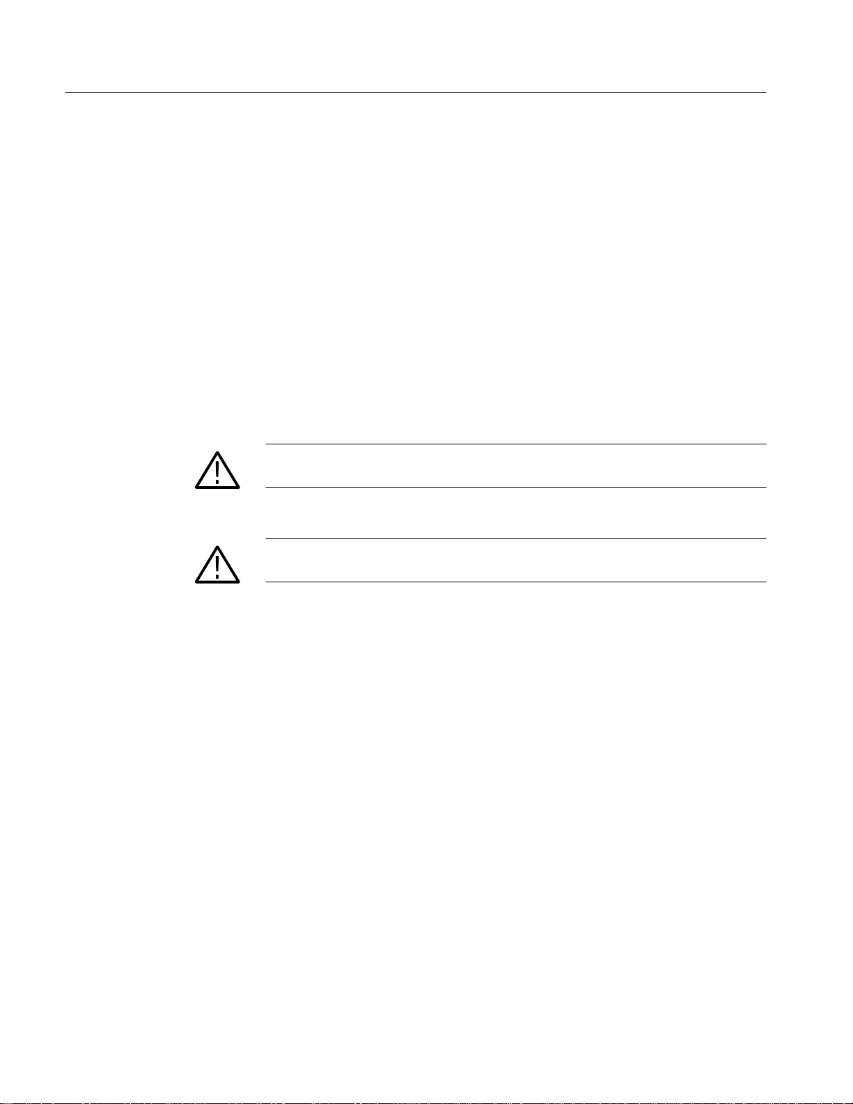
User Interface 1–2. . . . . . . . . . . . . . . . . . . . . . . . . . . . . . . . . . . . . . . . . . . . . . . . . . . .
Signal Acquisition System 1–2. . . . . . . . . . . . . . . . . . . . . . . . . . . . . . . . . . . . . . . . . .
Horizontal System 1–3. . . . . . . . . . . . . . . . . . . . . . . . . . . . . . . . . . . . . . . . . . . . . . . .
Trigger System 1–4. . . . . . . . . . . . . . . . . . . . . . . . . . . . . . . . . . . . . . . . . . . . . . . . . . .
Acquisition Control 1–5. . . . . . . . . . . . . . . . . . . . . . . . . . . . . . . . . . . . . . . . . . . . . . .
On-Board User Assistance 1–6. . . . . . . . . . . . . . . . . . . . . . . . . . . . . . . . . . . . . . . . . .
Measurement Assistance 1–6. . . . . . . . . . . . . . . . . . . . . . . . . . . . . . . . . . . . . . . . . . .
Storage 1–7. . . . . . . . . . . . . . . . . . . . . . . . . . . . . . . . . . . . . . . . . . . . . . . . . . . . . . . . .
I/O 1–7. . . . . . . . . . . . . . . . . . . . . . . . . . . . . . . . . . . . . . . . . . . . . . . . . . . . . . . . . . . .
Display 1–8. . . . . . . . . . . . . . . . . . . . . . . . . . . . . . . . . . . . . . . . . . . . . . . . . . . . . . . . .
Nominal Traits 1–9. . . . . . . . . . . . . . . . . . . . . . . . . . . . . . . . . . . . . . . . . . . . .
Warranted Characteristics 1–15. . . . . . . . . . . . . . . . . . . . . . . . . . . . . . . . . . .
Typical Characteristics 1–23. . . . . . . . . . . . . . . . . . . . . . . . . . . . . . . . . . . . . .
Operational Information
Installation 2–1. . . . . . . . . . . . . . . . . . . . . . . . . . . . . . . . . . . . . . . . . . . . . . . .
Supplying Operating Power 2–1. . . . . . . . . . . . . . . . . . . . . . . . . . . . . . . . . . . . . . . . .
Operating Environment 2–3. . . . . . . . . . . . . . . . . . . . . . . . . . . . . . . . . . . . . . . . . . . .
Applying and Interrupting Power 2–3. . . . . . . . . . . . . . . . . . . . . . . . . . . . . . . . . . . .
Repackaging Instructions 2–4. . . . . . . . . . . . . . . . . . . . . . . . . . . . . . . . . . . . . . . . . . .
Installed Options 2–5. . . . . . . . . . . . . . . . . . . . . . . . . . . . . . . . . . . . . . . . . . . . . . . . .
Operating Instructions 2–7. . . . . . . . . . . . . . . . . . . . . . . . . . . . . . . . . . . . . .
Screen Layout 2–7. . . . . . . . . . . . . . . . . . . . . . . . . . . . . . . . . . . . . . . . . . . . . . . . . . . .
Basic Procedures 2–7. . . . . . . . . . . . . . . . . . . . . . . . . . . . . . . . . . . . . . . . . . . . . . . . .
Theory of Operation
Logic Conventions 3–1. . . . . . . . . . . . . . . . . . . . . . . . . . . . . . . . . . . . . . . . . . . . . . . .
Module Overview 3–1. . . . . . . . . . . . . . . . . . . . . . . . . . . . . . . . . . . . . . . . . . . . . . . . .
TDS 500B, TDS 600B and TDS 700A Service Manual
i

Table of Contents
Performance Verification
Input Channels vs. Model 4–2. . . . . . . . . . . . . . . . . . . . . . . . . . . . . . . . . . . . . . . . . .
Conventions 4–2. . . . . . . . . . . . . . . . . . . . . . . . . . . . . . . . . . . . . . . . . . . . . . . . . . . . .
Brief Procedures 4–5. . . . . . . . . . . . . . . . . . . . . . . . . . . . . . . . . . . . . . . . . . .
Self Tests 4–5. . . . . . . . . . . . . . . . . . . . . . . . . . . . . . . . . . . . . . . . . . . . . . . . . . . . . . .
Functional T ests 4–7. . . . . . . . . . . . . . . . . . . . . . . . . . . . . . . . . . . . . . . . . . . . . . . . . .
Performance Tests 4–15. . . . . . . . . . . . . . . . . . . . . . . . . . . . . . . . . . . . . . . . . .
Prerequisites 4–15. . . . . . . . . . . . . . . . . . . . . . . . . . . . . . . . . . . . . . . . . . . . . . . . . . . . .
Equipment Required 4–16. . . . . . . . . . . . . . . . . . . . . . . . . . . . . . . . . . . . . . . . . . . . . . .
TDS 600B T est Record 4–19. . . . . . . . . . . . . . . . . . . . . . . . . . . . . . . . . . . . . . . . . . . .
TDS 500B/700A T est Record 4–23. . . . . . . . . . . . . . . . . . . . . . . . . . . . . . . . . . . . . . .
Signal Acquisition System Checks 4–27. . . . . . . . . . . . . . . . . . . . . . . . . . . . . . . . . . .
Time Base System Checks 4–43. . . . . . . . . . . . . . . . . . . . . . . . . . . . . . . . . . . . . . . . . .
Trigger System Checks 4–45. . . . . . . . . . . . . . . . . . . . . . . . . . . . . . . . . . . . . . . . . . . .
Output Signal Checks 4–58. . . . . . . . . . . . . . . . . . . . . . . . . . . . . . . . . . . . . . . . . . . . . .
Option 05 Video Trigger Checks 4–67. . . . . . . . . . . . . . . . . . . . . . . . . . . . . . . . . . . . .
Sine Wave Generator Leveling Procedure 4–84. . . . . . . . . . . . . . . . . . . . . . . . . . . . . .
Adjustment Procedures
Maintenance
Options
Requirements for Performance 5–1. . . . . . . . . . . . . . . . . . . . . . . . . . . . . . . . . . . . . .
Usage 5–2. . . . . . . . . . . . . . . . . . . . . . . . . . . . . . . . . . . . . . . . . . . . . . . . . . . . . . . . . .
Equipment Required 5–5. . . . . . . . . . . . . . . . . . . . . . . . . . . . . . . . . . . . . . . . . . . . . . .
Adjustment Instructions 5–6. . . . . . . . . . . . . . . . . . . . . . . . . . . . . . . . . . . . . . . . . . . .
Probe Adjustment for the P6139A Probe 5–10. . . . . . . . . . . . . . . . . . . . . . . . . . . . . . .
Display Assembly Adjustment 5–20. . . . . . . . . . . . . . . . . . . . . . . . . . . . . . . . . . . . . . .
Related Maintenance Procedures 6–1. . . . . . . . . . . . . . . . . . . . . . . . . . . . . . . . . . . . .
Preparation 6–2. . . . . . . . . . . . . . . . . . . . . . . . . . . . . . . . . . . . . . . . . . . . . . . . . . . . . .
Inspection and Cleaning 6–4. . . . . . . . . . . . . . . . . . . . . . . . . . . . . . . . . . . . . . . . . . . .
Removal and Installation Procedures 6–9. . . . . . . . . . . . . . . . . . . . . . . . . .
Preparation — Please Read 6–9. . . . . . . . . . . . . . . . . . . . . . . . . . . . . . . . . . . . . . . . .
Access Procedure 6–15. . . . . . . . . . . . . . . . . . . . . . . . . . . . . . . . . . . . . . . . . . . . . . . . .
Procedures for External Modules 6–16. . . . . . . . . . . . . . . . . . . . . . . . . . . . . . . . . . . . .
Procedures for Outer-Chassis Modules 6–29. . . . . . . . . . . . . . . . . . . . . . . . . . . . . . . .
Procedures for Inner-Chassis Modules 6–46. . . . . . . . . . . . . . . . . . . . . . . . . . . . . . . .
Disassembly for Cleaning 6–53. . . . . . . . . . . . . . . . . . . . . . . . . . . . . . . . . . . . . . . . . .
Troubleshooting 6–57. . . . . . . . . . . . . . . . . . . . . . . . . . . . . . . . . . . . . . . . . . . .
Diagnostics 6–57. . . . . . . . . . . . . . . . . . . . . . . . . . . . . . . . . . . . . . . . . . . . . . . . . . . . . .
Firmware Updates 6–58. . . . . . . . . . . . . . . . . . . . . . . . . . . . . . . . . . . . . . . . . . . . . . . .
Electrical Parts List
Diagrams
Mechanical Parts LIst
ii
TDS 500B, TDS 600B and TDS 700A Service Manual

List of Figures
Table of Contents
Figure 2–1: Map of Display Functions 2–8. . . . . . . . . . . . . . . . . . . . . . . . .
Figure 4–1: Map of Display Functions 4–3. . . . . . . . . . . . . . . . . . . . . . . . .
Figure 4–2: Verifying Adjustments and Signal-Path Compensation 4–6.
Figure 4–3: Universal Test Hookup for Functional Tests –
TDS 600B Shown 4–8. . . . . . . . . . . . . . . . . . . . . . . . . . . . . . . . . . . . . . . .
Figure 4–4: Measurement of DC Offset Accuracy at Zero Setting 4–29. . .
Figure 4–5: Initial Test Hookup 4–30. . . . . . . . . . . . . . . . . . . . . . . . . . . . . . .
Figure 4–6: Measurement of DC Accuracy at Maximum Offset
and Position 4–32. . . . . . . . . . . . . . . . . . . . . . . . . . . . . . . . . . . . . . . . . . . .
Figure 4–7: Initial Test Hookup 4–34. . . . . . . . . . . . . . . . . . . . . . . . . . . . . . .
Figure 4–8: Optional Initial Test Hookup 4–34. . . . . . . . . . . . . . . . . . . . . . .
Figure 4–9: Measurement of Analog Bandwidth 4–37. . . . . . . . . . . . . . . . .
Figure 4–10: Initial Test Hookup 4–39. . . . . . . . . . . . . . . . . . . . . . . . . . . . . .
Figure 4–11: Measurement of Channel Delay – TDS 684B Shown 4–41. .
Figure 4–12: Initial Test Hookup 4–43. . . . . . . . . . . . . . . . . . . . . . . . . . . . . .
Figure 4–13: Measurement of Accuracy — Long-Term and
Delay Time 4–45. . . . . . . . . . . . . . . . . . . . . . . . . . . . . . . . . . . . . . . . . . . . .
Figure 4–14: Initial Test Hookup 4–46. . . . . . . . . . . . . . . . . . . . . . . . . . . . . .
Figure 4–15: Measurement of Time Accuracy for Pulse and
Glitch Triggering 4–48. . . . . . . . . . . . . . . . . . . . . . . . . . . . . . . . . . . . . . . .
Figure 4–16: Initial Test Hookup 4–49. . . . . . . . . . . . . . . . . . . . . . . . . . . . . .
Figure 4–17: Measurement of Trigger-Level Accuracy 4–51. . . . . . . . . . . .
Figure 4–18: Initial Test Hookup 4–54. . . . . . . . . . . . . . . . . . . . . . . . . . . . . .
Figure 4–19: Measurement of Trigger Sensitivity — 50 MHz Results
Shown on a TDS 684B Screen 4–55. . . . . . . . . . . . . . . . . . . . . . . . . . . . .
Figure 4–20: Initial Test Hookup 4–58. . . . . . . . . . . . . . . . . . . . . . . . . . . . . .
Figure 4–21: Measurement of Main Trigger Out Limits 4–60. . . . . . . . . . .
Figure 4–22: Initial Test Hookup 4–62. . . . . . . . . . . . . . . . . . . . . . . . . . . . . .
Figure 4–23: Measurement of Probe Compensator Frequency 4–64. . . . .
Figure 4–24: Subsequent Test Hookup 4–65. . . . . . . . . . . . . . . . . . . . . . . . .
Figure 4–25: Measurement of Probe Compensator Amplitude 4–66. . . . .
Figure 4–26: Jitter Test Hookup 4–68. . . . . . . . . . . . . . . . . . . . . . . . . . . . . .
Figure 4–27: Jitter Test Displayed Waveform – TDS 684B Shown 4–69. .
Figure 4–28: Jitter Test When Completed – TDS 684B Shown 4–70. . . . .
TDS 500B, TDS 600B and TDS 700A Service Manual
iii

Table of Contents
Figure 4–29: Triggered Signal Range Test – 300 mV 4–72. . . . . . . . . . . . . .
Figure 4–30: Triggered Signal Range Test – 75 mV 4–73. . . . . . . . . . . . . . .
Figure 4–31: 60 Hz Rejection Test Hookup 4–74. . . . . . . . . . . . . . . . . . . . . .
Figure 4–32: 60 Hz Rejection Test Setup Signal 4–74. . . . . . . . . . . . . . . . . .
Figure 4–33: Subsequent 60 Hz Rejection Test Hookup 4–75. . . . . . . . . . .
Figure 4–34: 60 Hz Rejection Test Result – TDS 684B Shown 4–76. . . . . .
Figure 4–35: Line Count Accuracy Test Hookup 4–77. . . . . . . . . . . . . . . . .
Figure 4–36: Line Count Accuracy Test Setup Waveform – TDS 684B
Shown 4–78. . . . . . . . . . . . . . . . . . . . . . . . . . . . . . . . . . . . . . . . . . . . . . . . .
Figure 4–37: Line Count Accuracy Correct Result Waveform 4–79. . . . . .
Figure 4–38: Setup for Sync Duty Cycle Test 4–81. . . . . . . . . . . . . . . . . . . .
Figure 4–39: Sync Duty Cycle Test: One-Div Neg Pulse Waveform 4–82. .
Figure 4–40: Sync Duty Cycle Test: Critically Adjusted Pulse 4–83. . . . . .
Figure 4–41: Sine Wave Generator Leveling Equipment Setup 4–85. . . . .
Figure 4–42: Equipment Setup for Maximum Amplitude 4–86. . . . . . . . .
Figure 5–1: Accessing the Protection Switch 5–9. . . . . . . . . . . . . . . . . . . .
Figure 5–2: Hookup for Probe Compensation 5–10. . . . . . . . . . . . . . . . . . .
Figure 5–3: Performing Probe Compensation 5–11. . . . . . . . . . . . . . . . . . .
Figure 5–4: Proper and Improper Probe Compensation 5–12. . . . . . . . . . .
Figure 5–5: Exposing the Inner Probe Tip 5–13. . . . . . . . . . . . . . . . . . . . . .
Figure 5–6: Initial Test Hookup 5–13. . . . . . . . . . . . . . . . . . . . . . . . . . . . . . .
Figure 5–7: Exposing the Probe Body 5–16. . . . . . . . . . . . . . . . . . . . . . . . . .
Figure 5–8: Initial Test Hookup 5–16. . . . . . . . . . . . . . . . . . . . . . . . . . . . . . .
Figure 5–9: Locations of P6139A Probe Adjustments 5–18. . . . . . . . . . . . .
Figure 5–10: Adjustments versus Front-Corner Response 5–19. . . . . . . . .
Figure 5–11: Five and Ten Percent Luminance Patches 5–21. . . . . . . . . . .
Figure 6–1: External Modules 6–12. . . . . . . . . . . . . . . . . . . . . . . . . . . . . . . .
Figure 6–2: Outer-Chassis Modules 6–13. . . . . . . . . . . . . . . . . . . . . . . . . . .
Figure 6–3: Inner-Chassis Modules 6–14. . . . . . . . . . . . . . . . . . . . . . . . . . . .
Figure 6–4: Knob Removal 6–17. . . . . . . . . . . . . . . . . . . . . . . . . . . . . . . . . . .
Figure 6–5: Line Fuse and Line Cord Removal 6–18. . . . . . . . . . . . . . . . . .
Figure 6–6: Rear Cover and Cabinet Removal 6–21. . . . . . . . . . . . . . . . . .
Figure 6–7: Front Cover, Trim Ring, Menu Buttons, and
Attenuator Panel Removal (Front Cover not Shown) 6–22. . . . . . . . . .
Figure 6–8: A12 Front-Panel Assembly Removal 6–24. . . . . . . . . . . . . . . . .
Figure 6–9: Disassembly of Front-Panel Assembly 6–25. . . . . . . . . . . . . . .
Figure 6–10: Cabinet Modules Removal 6–28. . . . . . . . . . . . . . . . . . . . . . . .
iv
TDS 500B, TDS 600B and TDS 700A Service Manual

Table of Contents
Figure 6–11: A14 D1 Bus and Analog-Power and Digital-Power Cables
Removal 6–30. . . . . . . . . . . . . . . . . . . . . . . . . . . . . . . . . . . . . . . . . . . . . . .
Figure 6–12: Remove Circuit Board Assembly From Oscilloscope 6–31. .
Figure 6–13: Remove Circuit Board From Assembly 6–32. . . . . . . . . . . . .
Figure 6–14: Circuit Board Installed 6–34. . . . . . . . . . . . . . . . . . . . . . . . . . .
Figure 6–15: Circuit Board Removal 6–35. . . . . . . . . . . . . . . . . . . . . . . . . .
Figure 6–16: A11 Processor/Display Removal 6–37. . . . . . . . . . . . . . . . . . .
Figure 6–17: Board Bracket Removal 6–38. . . . . . . . . . . . . . . . . . . . . . . . . .
Figure 6–18: A10 Acquisition Board Removal 6–41. . . . . . . . . . . . . . . . . . .
Figure 6–19: Floppy Disk Removal 6–43. . . . . . . . . . . . . . . . . . . . . . . . . . . .
Figure 6–20: Rear Chassis Removal 6–45. . . . . . . . . . . . . . . . . . . . . . . . . . .
Figure 6–21: A16 Low Voltage Power Supply Removal 6–47. . . . . . . . . . .
Figure 6–22: Display Assembly Removal 6–49. . . . . . . . . . . . . . . . . . . . . . .
Figure 6–23: Display Driver Board Removal 6–50. . . . . . . . . . . . . . . . . . . .
Figure 6–24: Front Subpanel Removal 6–52. . . . . . . . . . . . . . . . . . . . . . . . .
Figure 6–25: Accessing the Protection Switch 6–58. . . . . . . . . . . . . . . . . . .
Figure 6–26: Primary Troubleshooting Procedure 6–59. . . . . . . . . . . . . . .
Figure 6–27: Module Isolation Troubleshooting Procedure 6–61. . . . . . . .
Figure 6–28: A16 Low Voltage Power Supply Module Isolation
Troubleshooting Procedure 6–62. . . . . . . . . . . . . . . . . . . . . . . . . . . . . . .
Figure 6–29: Power Supply Voltage Measurement Locations 6–63. . . . . . .
Figure 6–30: Color Display Troubleshooting Procedure 6–64. . . . . . . . . . .
Figure 6–31: Horizontal and Vertical Sync Signals – Color Display 6–65.
Figure 6–32: A Video Signal with White, Black, and Blanking Levels –
Color Display 6–65. . . . . . . . . . . . . . . . . . . . . . . . . . . . . . . . . . . . . . . . . . .
Figure 6–33: Processor/Acquisition Troubleshooting Procedure 6–66. . . .
Figure 6–34: Processor/Front Panel Troubleshooting Procedure 6–67. . . .
Figure 6–35: Attenuator/Acquisition Troubleshooting Procedure 6–68. . .
Figure 6–36: A11 DRAM Processor/Display Module (View of
Right Side) 6–70. . . . . . . . . . . . . . . . . . . . . . . . . . . . . . . . . . . . . . . . . . . . .
Figure 6–37: A11 DRAM Processor/Display Module (View of
Upper Left Corner) 6–71. . . . . . . . . . . . . . . . . . . . . . . . . . . . . . . . . . . . . .
Figure 6–38: A11 DRAM Processor/Display Module (View of
Lower Left Corner) 6–71. . . . . . . . . . . . . . . . . . . . . . . . . . . . . . . . . . . . . .
Figure 6–39: A10 Acquisition Module (View of Lower Right Corner) 6–72
Figure 9–1: Interconnections 9–2. . . . . . . . . . . . . . . . . . . . . . . . . . . . . . . . .
Figure 9–2: Block Diagram 9–4. . . . . . . . . . . . . . . . . . . . . . . . . . . . . . . . . . .
Figure 10–1: External Modules 10–7. . . . . . . . . . . . . . . . . . . . . . . . . . . . . . .
TDS 500B, TDS 600B and TDS 700A Service Manual
v

Table of Contents
Figure 10–2: Outer-Chassis Modules 10–9. . . . . . . . . . . . . . . . . . . . . . . . . .
Figure 10–3: Inner-Chassis Modules 10–11. . . . . . . . . . . . . . . . . . . . . . . . . . .
Figure 10–4: Cables, Bottom View 10–13. . . . . . . . . . . . . . . . . . . . . . . . . . . . .
Figure 10–5: Cables, Top View 10–15. . . . . . . . . . . . . . . . . . . . . . . . . . . . . . . .
Figure 10–6: Floppy Disk 10–17. . . . . . . . . . . . . . . . . . . . . . . . . . . . . . . . . . . .
Figure 10–7: Accessories 10–19. . . . . . . . . . . . . . . . . . . . . . . . . . . . . . . . . . . . .
vi
TDS 500B, TDS 600B and TDS 700A Service Manual

List of Tables
Table of Contents
Table 1–1: Key Features of the TDS 500B, 600B and
700A Oscilloscopes 1–1. . . . . . . . . . . . . . . . . . . . . . . . . . . . . . . . . . . . . .
Table 1–2: Record Length and Divisions per Record vs. TDS Model 1–4
Table 1–3: Nominal Traits — Signal Acquisition System 1–9. . . . . . . . . .
Table 1–4: Nominal Traits — Time Base System 1–10. . . . . . . . . . . . . . . .
Table 1–5: Nominal Traits — Triggering System 1–11. . . . . . . . . . . . . . . .
Table 1–6: Nominal Traits — Display System 1–12. . . . . . . . . . . . . . . . . . .
Table 1–7: Nominal Traits — GPIB Interface, Output Ports, and
Power Fuse 1–12. . . . . . . . . . . . . . . . . . . . . . . . . . . . . . . . . . . . . . . . . . . .
Table 1–8: Nominal Traits — Data Handling and Reliability 1–12. . . . . .
Table 1–9: Nominal Traits — Mechanical 1–13. . . . . . . . . . . . . . . . . . . . . .
Table 1–10: Warranted Characteristics — Signal Acquisition
System 1–16. . . . . . . . . . . . . . . . . . . . . . . . . . . . . . . . . . . . . . . . . . . . . . . .
Table 1–11: Warranted Characteristics — Time Base System 1–17. . . . . .
Table 1–12: Warranted Characteristics — Triggering System 1–18. . . . .
Table 1–13: Warranted Characteristics — Output Ports, Probe
Compensator, and Power Requirements 1–18. . . . . . . . . . . . . . . . . . . .
Table 1–14: Warranted Characteristics — Environmental 1–19. . . . . . . .
Table 1–15: Certifications and Compliances 1–21. . . . . . . . . . . . . . . . . . . .
Table 1–16: Typical Characteristics — Signal Acquisition System 1–23. .
Table 1–17: Typical Characteristics — Triggering System 1–26. . . . . . . .
Table 2–1: Power-Cord Conductor Identification 2–2. . . . . . . . . . . . . . . .
Table 2–2: Power Cord Identification 2–2. . . . . . . . . . . . . . . . . . . . . . . . .
Table 2–3: Effects of Corrupted Data 2–4. . . . . . . . . . . . . . . . . . . . . . . . . .
Table 4–1: Test Equipment 4–16. . . . . . . . . . . . . . . . . . . . . . . . . . . . . . . . . .
TDS 600B Test Record 4–19. . . . . . . . . . . . . . . . . . . . . . . . . . . . . . . . . . . . . .
TDS 500B/700A Test Record 4–23. . . . . . . . . . . . . . . . . . . . . . . . . . . . . . . . .
Table 4–2: DC Offset Accuracy (Zero Setting) 4–28. . . . . . . . . . . . . . . . . .
Table 4–3: DC Voltage Measurement Accuracy 4–31. . . . . . . . . . . . . . . . .
Table 4–4: Analog Bandwidth 4–35. . . . . . . . . . . . . . . . . . . . . . . . . . . . . . . .
Table 4–5: Delay Between Channels Worksheet 4–42. . . . . . . . . . . . . . . . .
Table 5–1: Calibration Tests 5–3. . . . . . . . . . . . . . . . . . . . . . . . . . . . . . . . .
Table 5–2: Adjustments Required for Module Replaced 5–4. . . . . . . . . .
Table 5–3: Adjustments and Dependencies 5–4. . . . . . . . . . . . . . . . . . . . .
TDS 500B, TDS 600B and TDS 700A Service Manual
vii

Table of Contents
Table 5–4: Test Equipment, Fixtures, and Supplies 5–5. . . . . . . . . . . . . .
Table 5–5: GPIB Board Configuration 5–7. . . . . . . . . . . . . . . . . . . . . . . . .
Table 6–1: Relative Susceptibility to Static-Discharge Damage 6–2. . . . .
Table 6–2: External Inspection Check List 6–5. . . . . . . . . . . . . . . . . . . . .
Table 6–3: Internal Inspection Check List 6–6. . . . . . . . . . . . . . . . . . . . . .
Table 6–4: Tools Required for Module Removal 6–11. . . . . . . . . . . . . . . . .
Table 6–5: Normal Supply Voltages (Measured on J26 and J27 on
the A11 DRAM Processor/Display Module) 6–63. . . . . . . . . . . . . . . . . .
Table 6–6: No-Load Supply Voltages (Measured on J5 and J6 on
the A17 Main LV Power Supply Module) 6–63. . . . . . . . . . . . . . . . . . . .
Table 7–1: Options 7–1. . . . . . . . . . . . . . . . . . . . . . . . . . . . . . . . . . . . . . . . .
Table 7–2: Standard Accessories 7–4. . . . . . . . . . . . . . . . . . . . . . . . . . . . . .
Table 7–3: Optional Accessories 7–5. . . . . . . . . . . . . . . . . . . . . . . . . . . . . .
Table 7–4: Accessory Software 7–7. . . . . . . . . . . . . . . . . . . . . . . . . . . . . . .
viii
TDS 500B, TDS 600B and TDS 700A Service Manual

General Safety Summary
Review the following safety precautions to avoid injury and prevent damage to
this product or any products connected to it. To avoid potential hazards, use the
product only as specified.
Only qualified personnel should perform service procedures.
Injury Precautions
Use Proper Power Cord
Avoid Electric Overload
Ground the Product
Do Not Operate Without
Covers
Use Proper Fuse
Do Not Operate in
Wet/Damp Conditions
Do Not Operate in
Explosive Atmosphere
To avoid fire hazard, use only the power cord specified for this product.
To avoid electric shock or fire hazard, do not apply a voltage to a terminal that is
outside the range specified for that terminal.
This product is grounded through the grounding conductor of the power cord. To
avoid electric shock, the grounding conductor must be connected to earth ground.
Before making connections to the input or output terminals of the product, ensure
that the product is properly grounded.
To avoid electric shock or fire hazard, do not operate this product with covers or
panels removed.
To avoid fire hazard, use only the fuse type and rating specified for this product.
To avoid electric shock, do not operate this product in wet or damp conditions.
To avoid injury or fire hazard, do not operate this product in an explosive
atmosphere.
Keep Probe Surface Clean
To avoid electric shock and erroneous readings, keep probe surface clean.
Product Damage Precautions
Use Proper Power Source
TDS 500B, TDS 600B and TDS 700A Service Manual
Do not operate this product from a power source that applies more than the
voltage specified.
ix
General Safety Summary
Provide Proper Ventilation
Do Not Operate With
Suspected Failures
Do Not Immerse in
To prevent product overheating, provide proper ventilation.
If you suspect there is damage to this product, have it inspected by qualified
service personnel.
Clean the probe using only a damp cloth. Refer to cleaning instructions.
Liquids
Safety Terms and Symbols
Terms in This Manual
These terms may appear in this manual:
WARNING. Warning statements identify conditions or practices that could result
in injury or loss of life.
CAUTION. Caution statements identify conditions or practices that could result in
damage to this product or other property.
Terms on the Product
x
These terms may appear on the product:
DANGER indicates an injury hazard immediately accessible as you read the
marking.
WARNING indicates an injury hazard not immediately accessible as you read the
marking.
CAUTION indicates a hazard to property including the product.
TDS 500B, TDS 600B and TDS 700A Service Manual

General Safety Summary
Symbols on the Product
The following symbols may appear on the product:
DANGER
High Voltage
Certifications and Compliances
CSA Certified Power
Cords
Certifications and
Compliances
CSA Certification includes the products and power cords appropriate for use in
the North America power network. All other power cords supplied are approved
for the country of use.
Refer to the specifications section for a listing of certifications and compliances
that apply to this product.
Protective Ground
(Earth) T erminal
ATTENTION
Refer to
Manual
Double
Insulated
TDS 500B, TDS 600B and TDS 700A Service Manual
xi

General Safety Summary
xii
TDS 500B, TDS 600B and TDS 700A Service Manual

Service Safety Summary
Only qualified personnel should perform service procedures. Read this Service
Safety Summary and the General Safety Summary before performing any service
procedures.
Do Not Service Alone
Disconnect Power
Use Caution When
Servicing the CRT
Use Care When Servicing
With Power On
Do not perform internal service or adjustments of this product unless another
person capable of rendering first aid and resuscitation is present.
To avoid electric shock, disconnect the main power by means of the power cord
or, if provided, the power switch.
To avoid electric shock or injury, use extreme caution when handling the CRT.
Only qualified personnel familiar with CRT servicing procedures and precautions
should remove or install the CRT.
CRTs retain hazardous voltages for long periods of time after power is turned off.
Before attempting any servicing, discharge the CRT by shorting the anode to
chassis ground. When discharging the CRT, connect the discharge path to ground
and then the anode. Rough handling may cause the CRT to implode. Do not nick
or scratch the glass or subject it to undue pressure when removing or installing it.
When handling the CRT, wear safety goggles and heavy gloves for protection.
Dangerous voltages or currents may exist in this product. Disconnect power,
remove battery (if applicable), and disconnect test leads before removing
protective panels, soldering, or replacing components.
To avoid electric shock, do not touch exposed connections.
X-Radiation
TDS 500B, TDS 600B and TDS 700A Service Manual
To avoid x-radiation exposure, do not modify or otherwise alter the high-voltage
circuitry or the CRT enclosure. X-ray emissions generated within this product
have been sufficiently shielded.
xiii

Service Safety Summary
xiv
TDS 500B, TDS 600B and TDS 700A Service Manual

Preface
Manual Structure
This preface contains information needed to properly use this manual to service
the TDS 500B, TDS 600B and TDS 700A Digitizing Oscilloscopes, as well as
general information critical to safe and effective servicing of this oscilloscope.
The following models are covered:
TDS 500B: TDS 520B and TDS 540B
TDS 600B: TDS 620B, TDS 644B, TDS 680B, and TDS 684B
TDS 700A: TDS 724A, TDS 754A, TDS 782A, and TDS 784A
This manual is divided into sections, such as Specification and Theory of
Operation. Further, it is divided into subsections, such as Product Description
and Removal and Installation Procedures.
Sections containing procedures also contain introductions to those procedures. Be
sure to read these introductions because they provide information needed to do
the service correctly and efficiently. The following is a brief description of each
manual section.
H Specification contains a product description of the TDS 500B, TDS 600B
and TDS 700A Digitizing Oscilloscopes and tables of the characteristics and
descriptions that apply to it.
H Operating Information includes general information and operating instruc-
tions at the level needed to safely power on and service this oscilloscope. A
statement of the service strategy that this manual supports, and instructions
for shipment of the Digitizing Oscilloscopes are found in this section.
H Theory of Operation contains circuit descriptions that support general service
and fault isolation.
H Performance Verification contains a collection of procedures for confirming
that these Digitizing Oscilloscopes function properly and meet warranted
limits.
H Adjustment Procedures contains a collection of procedures for adjusting
these Digitizing Oscilloscopes to meet warranted limits.
H Maintenance contains information and procedures for doing preventive and
corrective maintenance of these Digitizing Oscilloscopes. Instructions for
TDS 500B, TDS 600B and TDS 700A Service Manual
xv

Preface
Manual Conventions
cleaning, for module removal and installation, and for fault isolation to a
module are found here.
H Options contains information on servicing any of the factory-installed
options that may be present in your oscilloscope.
H Electrical Parts List contains a statement referring you to Mechanical
Replaceable Parts, where both electrical and mechanical modules are listed.
H Diagrams contains a block diagram and an interconnection diagram useful
for isolating failed modules.
H Mechanical Parts List includes a table of all replaceable modules, their
descriptions, and their Tektronix part numbers.
This manual uses certain conventions which you should become familiar with
before doing service.
Modules
Channels
Safety
Symbols
Throughout this manual, any replaceable component, assembly, or part of these
Digitizing Oscilloscopes is referred to generically as a module. In general, a
module is an assembly, like a circuit board, rather than a component, like a
resistor or an integrated circuit. Sometimes a single component is a module; for
example, each chassis part of the oscilloscope is a module.
Some TDS models have two auxiliary channels called AUX 1 and AUX 2,
instead of CH 3 and CH 4. References to these channels default to CH 3 and
CH 4; if your oscilloscope is one of models TDS 520B, TDS 620B, TDS 680B,
TDS 724A, or TDS 782A, read AUX 1 and AUX 2 respectively for all references
to CH 3 and CH 4 in this manual.
Symbols and terms related to safety appear in the Safety Summary found at the
beginning of this manual.
Besides the symbols related to safety, this manual uses the following symbols:
STOP. The stop labels information which must be read in order to correctly do
service and to avoid incorrectly using or applying service procedures.
xvi
The clock icon labels procedure steps which require a pause to wait for
the oscilloscope to complete some operation before you can continue.
TDS 500B, TDS 600B and TDS 700A Service Manual

Related Manuals
Preface
Various icons such as the example icon at the left are used in procedures
to help identify certain readouts and menu functions on screen.
The TDS 500B, TDS 600B and TDS 700A Digitizing Oscilloscopes come with
the following manuals:
TDS 500B, TDS 600B & 700A User Manual (Tektronix part number
070-9719-XX) contains a tutorial to quickly show you how to operate the
TDS 500B, TDS 600B and TDS 700A Digitizing Oscilloscopes and an in depth
discussion of how to more completely use their features. Applications are also
discussed.
TDS 500B, TDS 600B & TDS 700A Reference (Tektronix part number
070-9382-XX) contains a brief overview of oscilloscope operation.
TDS Family (400A, 500B, 600B, and 700A) Programmer Manual (Tektronix part
number 070-9556-XX) contains information for programmed operation via the
GPIB interface. Included are the complete command set, setup information, and
programming examples.
TDS 500B, TDS 600B & TDS 700A Technical Reference (Tektronix part number
070-9729-XX) contains performance verification procedures and specifications.
TDS 500B, TDS 600B and TDS 700A Service Manual
xvii

Preface
xviii
TDS 500B, TDS 600B and TDS 700A Service Manual

Introduction
Service Strategy
STOP. Throughout this manual, any field-replaceable component, assembly, or
part of this oscilloscope is referred to generically as a module.
This manual contains all the information needed for periodic maintenance of the
TDS 500B, TDS 600B and TDS 700A Digitizing Oscilloscopes. (Examples of
such information are procedures for checking performance and for readjustment.)
Further, it contains all information for corrective maintenance down to the
module level. This means that the procedures, diagrams, and other troubleshooting aids help isolate failures to a specific module, rather than to components of
that module. Once a failure is isolated, replace the module with a fresh unit
obtained from the factory.
All modules are listed in Mechanical Parts List. To isolate a failure to a module,
use the fault isolation procedures found in Section 6, Maintenance Information.
To remove and replace any failed module, follow the instructions in Removal and
Installation Procedures, also found in Section 6.
Service Offerings
Warranty Repair Service
Repair or Calibration
Service
Tektronix provides service to cover repair under warranty as well as other
services that may provide a cost-effective answer to your service needs.
Whether providing warranty repair service or any of the other services listed
below, Tektronix service technicians, trained on Tektronix products, are best
equipped to service your TDS 500B, TDS 600B and TDS 700A Digitizing
Oscilloscopes. Tektronix technicians are appraised of the latest information on
improvements to the product as well as the latest new options to the product.
Tektronix warrants this product for three years from date of purchase, excluding
probes for which the warranty is one year. (The warranty appears after the title
page and copyright page in this manual.) Tektronix technicians provide warranty
service at most Tektronix service locations worldwide. Your Tektronix product
catalog lists all service locations worldwide.
The following services may be purchased to tailor repair and/or calibration of
your TDS 500B, TDS 600B and TDS 700A Digitizing Oscilloscopes to fit your
requirements.
TDS 500B, TDS 600B and TDS 700A Service Manual
xix

Introduction
At-Depot Service. Tektronix offers several standard-priced adjustment (calibration) and repair services:
H A single repair and/or adjustment.
H Calibrations using equipment and procedures that meet the traceability
standards specific to the local area.
H Annual maintenance agreements that provide for either calibration and repair
or calibration only of the oscilloscope.
Of these services, the annual maintenance agreement offers a particularly
cost-effective approach to service for many owners of the TDS 500B, TDS 600B
and TDS 700A Digitizing Oscilloscopes. Such agreements can be purchased to
span several years.
On-Site Service. The annual maintenance agreement can be purchased with
on-site service, with repair and calibration done at your facility. This service
reduces the time your oscilloscope is out of service when calibration or repair is
required.
Self Service
Before You Begin
Tektronix supports repair to the module level by providing Module Exchange and
Module Repair and Return.
Module Exchange. This service reduces down time for repair by allowing you to
exchange most modules for remanufactured ones. Tektronix ships you an updated
and tested exchange module from the Beaverton, Oregon service center, typically
within 24 hours. Each module comes with a 90-day service warranty.
Module Repair and Return. This service returns to you within 10 days the same
module that you shipped to Tektronix. The module shipped is repaired, tested,
and returned to you from the Beaverton, Oregon service center. It is not updated
to match current modules of the same type. Again, each module comes with a
90-day service warranty.
For More Information. Contact your local Tektronix service center or sales
engineer for more information on any of the repair or adjustment services just
described.
xx
This manual is for servicing the TDS 500B, TDS 600B and TDS 700A Digitizing
Oscilloscopes. To prevent injury to yourself or damage to the oscilloscope, do the
following tasks before you attempt service:
TDS 500B, TDS 600B and TDS 700A Service Manual

Introduction
H Be sure you are a qualified service person.
H Read the Safety Summary found at the beginning of this manual.
H Read Service Strategy in this section and Supplying Operating Power in
section 2.
When using this manual for servicing, be sure to heed all warnings, cautions, and
notes.
TDS 500B, TDS 600B and TDS 700A Service Manual
xxi

Introduction
xxii
TDS 500B, TDS 600B and TDS 700A Service Manual


Specifications
Product Description
This section begins with a general description of the traits of the TDS 500B, TDS
600B, and TDS 700A oscilloscopes. Three sections follow, one for each of three
classes of traits: nominal traits, warranted characteristics, and typical character-
istics.
The TDS 500B, TDS 600B and TDS 700A Digitizing Oscilloscopes are portable,
four-channel instruments suitable for use in a variety of test and measurement
applications and systems. Table 1–1 lists key features.
T able 1–1: Key Features of the TDS 500B, 600B and 700A Oscilloscopes
Feature TDS 600B TDS 500B & TDS 700A
Digitizing rate,
maximum
TDS 684B: 5 GS/s on each of 4 ch
TDS 680B: 5 GS/s on each of 2 ch
TDS 644B: 2.5 GS/s on each of 4 ch
TDS 620B: 2.5 GS/s on each of 2 ch
TDS 784A: 4 GS/s
TDS 540B, 754A, 782A: 2 GS/s
TDS 520B, 724A: 1 GS/s
Opt. 1G, TDS 540B: 1 GS/s
Analog bandwidth TDS 680B, 684B, 782A and 784A: 1 GHz
TDS 520B, 540B, 620B, 644B, 724A and 754A: 500 MHz
No. of Channels TDS 644B & 684B: 4
TDS 620B & 680B: 2 + 2
Record lengths,
maximum
Acquisition modes Sample, envelope, peak detect and
Trigger modes Include: edge, logic, and pulse.
Display TDS 520B, 540B, 620B, 680B: Monochrome
Storage 1.44 Mbyte, 3.5 inch, DOS 3.3-or-later floppy disk (optional on TDS 520B,
I/O Full GPIB programmability.
1
Two plus Two channel operation allows up to two of the four channels to be displayed
simultaneously. Channels not displayed can be used to couple a triggering signal to
the oscilloscope.
15,000 samples 50,000 samples
average
Video trigger , with option 05, modes include:
NTSC, SECAM, PAL, HDTV, and FlexFormat.
TDS 644B, 684B, 724A, 754A, 782A, 784A: Color
540B, 620B & 680B).
NVRAM storage for saving waveforms, hardcopies, and setups
Hardcopy output using GPIB, RS-232, or Centronics ports
1
TDS 540B, 754A & 784A: 4
TDS 520B, 724A & 782A: 2 + 2
(500,000 with option 1M)
Sample, envelope, average,
high-resolution, and
peak-detect
1
TDS 500B, TDS 600B and TDS 700A Service Manual
1–1

Specifications
User Interface
Use a combination of front-panel buttons, knobs, and on-screen menus to control
the many functions of the oscilloscope. The front-panel controls are grouped
according to function: vertical, horizontal, trigger, and special. Set a function you
adjust often, such as vertical positioning or the time base setting, directly by its
own front-panel knob. Set a function you change less often, such as vertical
coupling or horizontal mode, indirectly using a selected menu.
Menus
Indicators
General Purpose Knob
GUI
Pressing one (sometimes two) front-panel button(s), such as vertical menu,
displays a main menu of related functions, such as coupling and bandwidth, at
the bottom of the screen. Pressing a main-menu button, such as coupling,
displays a side menu of settings for that function, such as AC, DC, or GND
(ground) coupling, at the right side of the screen. Pressing a side-menu button
selects a setting such as DC.
On-screen readouts help you keep track of the settings for various functions, such
as vertical and horizontal scale and trigger level. Some readouts use the cursors
or the automatic parameter extraction feature (called measure) to display the
results of measurements made or the status of the instrument.
Assign the general purpose knob to adjust a selected parameter function. More
quickly change parameters by toggling the SHIFT button. Use the same method
as for selecting a function, except the final side-menu selection assigns the
general purpose knob to adjust some function, such as the position of measurement cursors on screen, or the setting for a channel fine gain.
The user interface also makes use of a GUI, or Graphical User Interface, to make
setting functions and interpreting the display more intuitive. Some menus and
status are displayed using iconic representations of function settings, such as
those shown here for full, 250 MHz and 20 MHz bandwidth. Such icons allow
you to more readily determine status or the available settings.
Signal Acquisition System
The signal acquisition system provides four, full-featured vertical channels with
calibrated vertical scale factors from 1 mV to 10 V per division. All channels can
be acquired simultaneously.
Each of the full-featured channels can be displayed, vertically positioned, and
offset, can have their bandwidth limited (250 MHz or 20 MHz) and their vertical
coupling specified. Fine gain can also be adjusted.
1–2
TDS 500B, TDS 600B and TDS 700A Service Manual

Horizontal System
Specifications
Besides these channels, up to three math waveforms and four reference
waveforms are available for display. (A math waveform results when you specify
dual waveform operations, such as add, on any two channels. A reference
waveform results when you save a waveform in a reference memory.)
There are three horizontal display modes: main only, main intensified, and
delayed only. You can select among various horizontal record length settings.
A feature called “Fit to Screen” allows you to view entire waveform records
within the 10 division screen area. Waveforms are compressed to fit on the
screen. See Table 1–2.
Both the delayed only display and the intensified zone on the main intensified
display may be delayed by time with respect to the main trigger. Both can be set
to display immediately after the delay (delayed runs after main mode). The
delayed display can also be set to display at the first valid trigger after the delay
(delayed-triggerable modes).
The delayed display (or the intensified zone) may also be delayed by a selected
number of events. In this case, the events source is the delayed-trigger source.
The delayed trigger can also be set to occur after a number of events plus an
amount of time.
TDS 500B, TDS 600B and TDS 700A Service Manual
1–3

Specifications
Model
Record
All TD
A
models; all channels
4
Optio
ot
Optio
ot
T able 1–2: Record Length and Divisions per Record vs. TDS Model
Divisions per Record
s
S 500B, TDS600B & TDS 700
n 1M equipped or n
n 1M equipped or n
TDS 500B & TDS 700A, all channels 50000 1,000 divs 10 divs
Length
500 10 divs 10 divs
1000 20 divs 10 divs
2500 50 divs 10 divs
5000 100 divs 10 divs
15000 300 divs 15 divs
FTS1 Off
2
FTS1 On
3
TDS 500B & TDS 700A, all channels
Option 1M equipped only
TDS 500B & TDS 700A, all channels
Option 1M equipped only
TDS 500B & TDS 700A, all channels
Option 1M equipped only
TDS 520B, TDS 724A & TDS 782A, one
channel only
TDS 540B, TDS 754A & TDS 784A, two
channels only
Option 1M equipped only
TDS 540B, TDS 754A & TDS 784A, one
channel only
Option 1M equipped only
1
Fit to Screen setting
2
Fit to Screen off preserves 50 samples/division in a 1–2–5 sec/division sequence.
3
Fit to Screen on lets the samples/division and the sec/division sequence vary.
4
All channels means all that may be displayed at one time: four channels for some
models, two for others. See Table 1–1 and its footnote on page 1–1.
75000 1,500 divs 15 divs
100000 2,000 divs 10 divs
130000 2,600 divs 13 divs
250000 5,000 divs 10 divs
500000 10,000 divs 10 divs
Trigger System
1–4
The triggering system supports a varied set of features for triggering the
signal-acquisition system. Trigger signals recognized include:
H Edge (main- and delayed-trigger systems): This familiar type of triggering is
fully configurable for source, slope, coupling, mode (auto or normal), and
holdoff.
TDS 500B, TDS 600B and TDS 700A Service Manual

Specifications
H Logic (main-trigger system): This type of triggering can be based on pattern
(asynchronous) or state (synchronous). In either case, logic triggering is
configurable for sources, for boolean operators to apply to those sources, for
logic pattern or state on which to trigger, for mode (auto or normal), and for
holdoff. Time qualification may be selected in pattern mode. Another class of
logic trigger, setup/hold, triggers when data in one trigger source changes
state within the setup and hold times that you specify relative to a clock in
another trigger source.
H Pulse (main-trigger system): Pulse triggering is configurable for triggering
on runt or glitch pulses, or on pulse widths or periods inside or outside limits
that you specify. It can also trigger on a pulse edge that has a slew rate faster
or slower than the rate you specify. The timeout trigger will act when events
do not occur in a defined time period. The pulse trigger is also configurable
for source, polarity, mode, and holdoff.
H Video (with option 05: Video Trigger): Video triggering is compatible with
standard NTSC, PAL, SECAM, and HDTV formats. An additional feature
called FlexFormat
format on which to trigger.
TM
(flexible format) allows the user to define the video
Acquisition Control
You can choose where the trigger point is located within the acquired waveform
record by selecting the amount of pretrigger data displayed. Presets of 10%, 50%,
and 90% of pretrigger data can be selected in the horizontal menu, or the general
purpose knob can be assigned to set pretrigger data to any value within the 0% to
100% limits.
You can specify a mode and manner to acquire and process signals that matches
your measurement requirements.
H Select the mode for interpolation (linear or sin (x)/x). This can increase the
apparent sample rate on the waveform when the maximum real-time rate is
exceeded.
H Use sample, envelope, average and peak detect modes to acquire signals.
With the TDS 500B/700A, also use high-resolution mode.
H Set the acquisition to stop after a single acquisition (or sequence of acquisi-
tions if acquiring in average or envelope modes) or after a limit condition has
been met.
H Select channel sources for compliance with limit tests. You can direct the
TDS to signal you or generate hard copy output either to a printer or to a
floppy-disk file based on the results. Also, you can create templates for use
in limit tests.
TDS 500B, TDS 600B and TDS 700A Service Manual
1–5

Specifications
On-Board User Assistance
Help and autoset can assist you in setting up the Digitizing Oscilloscope to make
your measurements.
Help
Autoset
Help displays operational information about any front-panel control. When help
mode is in effect, manipulating any front-panel control causes the Digitizing
Oscilloscope to display information about that control. When help is first
invoked, an introduction to help is displayed on screen.
Autoset automatically sets up the Digitizing Oscilloscope for a viewable display
based on the input signal.
Measurement Assistance
Once you have set up to make your measurements, the cursor and measure
features can help you quickly make those measurements.
Cursor
Three types of cursors are provided for making parametric measurements on the
displayed waveforms. Horizontal bar cursors (H Bar) measure vertical parameters (typically volts). Vertical bar cursors (V Bar) measure horizontal parameters
(typically time or frequency). Paired cursors measure both amplitude and time
simultaneously. These are delta measurements; that is, measurements based on
the difference between two cursors.
Both H Bar and V Bar cursors can also be used to make absolute measurements.
For the H Bars, either cursor can be selected to read out its voltage with respect
to any channel’s ground reference level. For the V Bars, the cursors measure time
with respect to the trigger point (event) of the acquisition. The cursors can also
control the portion of the waveform on which automatic measurements are made.
1–6
Measure
For time measurements, units can be either seconds or hertz (for 1/time).
With the video trigger option installed (Option 05), you can measure the video
line number using the vertical cursors. You can measure IRE amplitude (NTSC)
using the horizontal cursors with or without the video trigger option installed.
Measure can automatically extract parameters from the signal input to the
Digitizing Oscilloscope. Any four out of the 25 parameters available can be
displayed to the screen. The waveform parameters are measured continuously
with the results updated on-screen as the Digitizing Oscilloscope continues
to acquire waveforms.
TDS 500B, TDS 600B and TDS 700A Service Manual

Specifications
Digital Signal Processing
(DSP)
Storage
I/O
An important component of the multiprocessor architecture of this Digitizing
Oscilloscope is Tektronix’s proprietary digital signal processor, the DSP. This
dedicated processor supports advanced analysis of your waveforms when doing
such compute-intensive tasks as interpolation, waveform math, and signal
averaging. It also teams with a custom display system to deliver specialized
display modes (See Display, later in this description.)
Acquired waveforms may be saved in any of four nonvolatile REF (reference)
memories or on a 3.5 inch, DOS 3.3-or-later compatible disk. Any or all of the
saved waveforms may be displayed for comparison with the waveforms being
currently acquired.
The source and destination of waveforms to be saved may be chosen. You can
save any of the four channels to any REF memory or move a stored reference
from one REF memory to another. Reference waveforms may also be written into
a REF memory location via the GPIB interface.
The oscilloscope is fully controllable and capable of sending and receiving
waveforms over the GPIB interface (IEEE Std 488.1–1987/IEEE Std 488.2–1987
standard). This feature makes the instrument ideal for making automated
measurements in a production or research and development environment that
calls for repetitive data taking. Self-compensation and self-diagnostic features
built into the Digitizing Oscilloscope to aid in fault detection and servicing are
also accessible using commands sent from a GPIB controller.
The oscilloscope can also output copies of its display using the hardcopy feature.
This feature allows you to output waveforms and other on-screen information to
a variety of graphic printers and plotters from the TDS front panel, providing
hard copies without requiring you to put the TDS into a system-controller
environment. You can make hardcopies in a variety of popular output formats,
such as PCX, TIFF, BMP, RLE, EPS, Interleaf, and EPS mono or color. You can
also save hardcopies in a disk file in any of the formats above. The hardcopies
obtained are based on what is displayed on-screen at the time hardcopy is
invoked. The hardcopies can be stamped with date and time and spooled to a
queue for printing at a later time. You can output screen information via GPIB,
RS-232C, or Centronics interfaces.
TDS 500B, TDS 600B and TDS 700A Service Manual
1–7

Specifications
Display
The TDS 500B, TDS 600B and TDS 700A Digitizing Oscilloscopes offer
flexible display options. You can customize the following attributes of your
display:
H Color (TDS 644B, TDS 684B, and TDS 700A): Waveforms, readouts,
graticule, and variable persistence with color coding
H Intensity: waveforms, readouts, and graticule
H Style of waveform display(s): vectors or dots, intensified or nonintensified
samples, infinite persistence, and variable persistence
H Interpolation method: Sin(x)/x or Linear
H Display format: xy or yt with various graticule selections including NTSC
and PAL to be used with video trigger (option 05)
Zoom
This oscilloscope also provides an easy way to focus in on those waveform
features you want to examine up close. By invoking zoom, you can magnify the
waveform using the vertical and horizontal controls to expand (or contract) and
position it for viewing.
1–8
TDS 500B, TDS 600B and TDS 700A Service Manual

Nominal Traits
Ranges, Offset
This section contains a collection of tables that list the various nominal traits that
describe the TDS 500B, TDS 600B, and TDS 700A oscilloscopes. Electrical and
mechanical traits are included.
Nominal traits are described using simple statements of fact such as “Four, all
identical” for the trait “Input Channels, Number of,” rather than in terms of limits
that are performance requirements.
T able 1–3: Nominal Traits — Signal Acquisition System
Name Description
Bandwidth Selections 20 MHz, 250 MHz, and FULL
Samplers, Number of TDS 540B, 644B, 684B, 754A, and 784A: Four, simultaneous
TDS 520B, 620B, 680B, 724A, and 782A: Two, simultaneous
Digitized Bits, Number of 8 bits
Input Channels, Number of Four
Input Coupling DC, AC, or GND
Input Impedance Selections
1
1 M or 50
Volts/Div Setting Offset Range
1 mV/div – 100 mV/div
±1 V
101 mV/div – 1 V/div
1.01 V/div – 10 V/div
Range, Position ±5 divisions
Range, 1 M Sensitivity
Range, 50 Sensitivity
1
Displayed vertically with 25 digitization levels (DLs) per division and 10.24 divisions dynamic range with zoom off. A DL is
the smallest voltage level change of the oscilloscope input that can be resolved by the 8-bit A-D Converter. Expressed as a
voltage, a DL is equal to 1/25 of a division times the volts/division setting.
2
The sensitivity ranges from 1 mV/div to 10 V/div (for 1 M) or to 1 V/div (for 50 ) in a 1–2–5 sequence of coarse settings
with Fit-to-Screen off. Between coarse settings, the sensitivity can be finely adjusted with a resolution equal to 1% of the
more sensitive coarse setting. For example, between 50 mV/div and 100 mV/div, the volts/division can be set with 0.5 mV
resolution.
1 mV/div to 10 V/div
1 mV/div to 1 V/div
2
1
±10 V
±100 V
TDS 500B, TDS 600B and TDS 700A Service Manual
1–9

Nominal Traits
T able 1–4: Nominal Traits — Time Base System
Name Description
Range, Sample-Rate
1,3
TDS 684B: 5 Samples/sec to 5 GSamples/sec on four channels simultaneously
TDS 680B: 5 Samples/sec to 5 GSamples/sec on two channels simultaneously
TDS 644B: 5 Samples/sec to 2.5 GSamples/sec on four channels simultaneously
TDS 620B: 5 Samples/sec to 2.5 GSamples/sec on two channels simultaneously
TDS 520B and 724A: 5 Samples/sec to 1 GSamples/sec when acquiring 1 channel, to
500 MSamples/sec when acquiring 2 channels
TDS 540B and 782A: 5 Samples/sec to 2 GSamples/sec when acquiring 1 channel, to
1 G Sample/sec when acquiring 2 channels, or, for TDS 540B only, to 500 MSamples/sec
when acquiring 3 or 4 channels
TDS 540B with option 1G: 5 Samples/sec to 1 GSamples/sec when acquiring 1 channel, to
1 G Sample/sec when acquiring 2 channels, or to 500 MSamples/sec when acquiring 3 or
4 channels
TDS 754A: 5 Samples/sec to 2 GSamples/sec when acquiring 1 or 2 channels, to
1 GSamples/sec when acquiring 3 or 4 channels
TDS 784A: 5 Samples/sec to 4 GSamples/sec when acquiring 1 channel, to
2 G Sample/sec when acquiring 2 channels, or to 1 GSamples/sec when acquiring 3 or
4 channels
Range, Interpolated Waveform Rate
2,3
TDS 600B: 10 GSamples/sec to 250 GSamples/sec
TDS 520B, 540B, 724A, and 754A: 1 GSamples/sec to 100 GSamples/sec
TDS 782A and 784A: 2 GSamples/sec to 250 GSamples/sec
Range, Seconds/Division TDS 600B: 0.2 ns/div to 10 s/div
TDS 500B, 724A, and 754A: 0.5 ns/div to 10 s/div
TDS 782A and 784A: 0.2 ns/div to 10 s/div
Record Length Selection 500 samples, 1000 samples, 2500 samples 5000 samples, 15000 samples
The TDS 520B, 724A and 782A also offer: 50000 samples and, with option 1M, 75000,
100000, 130000 (1 or 2 channels), or 250000 (1 channel) samples
The TDS 540B, 754A, and 784A also offer: 50000 samples and, with option 1M, 75000,
100000, 130000, 250000 (1 or 2 channels), or 500000 (1 channel) samples
1
The range of real-time rates, expressed in samples/second, at which a digitizer samples signals at its inputs and stores the
samples in memory to produce a record of time-sequential samples.
2
The range of waveform rates for interpolated (or equivalent-time on the TDS 700A) waveform records.
3
The Waveform Rate (WR) is the equivalent sample rate of a waveform record. For a waveform record acquired by real-time
sampling of a single acquisition, the waveform rate is the same as the real-time sample rate; for a waveform created by
interpolation of real-time samples from a single acquisition or, on applicable products, the equivalent-time sampling of
multiple acquisitions, the waveform rate created is faster than the real time sample rate. For all these cases, the waveform
rate is 1/(Waveform Interval) for the waveform record, where the waveform interval (WI) is the time between the samples in
the waveform record.
1–10
TDS 500B, TDS 600B and TDS 700A Service Manual

T able 1–5: Nominal Traits — Triggering System
Ranges
et
Hol
Ra ges et a Hol o
imeSet
Hol
iolatio
igge
Ranges
igge
eshol
Name Description
Range, Delayed Trigger Time Delay 16 ns to 250 s
Range, Events Delay TDS 600B; 2 to 10,000,000
TDS 500B/700A: 1 to 10,000,000
Range (Time) for Pulse-Glitch, Pulse-Width,
Time-Qualified Runt, Timeout, or Slew Rate
Trigger, Delta Time
, S
up and
T
up/
d V
d for
n Tr
r
1 ns to 1 s
Feature Min to max
Setup Time
Nominal Traits
–100 ns to 100 ns
, Tr
r Level or Thr
Video Trigger Modes of Operation
(Option 05 Video Trigger)
Hold Time
Setup + Hold Time
For Setup Time, positive numbers mean a data transition before the clock edge and
negative means a transition after the clock edge.
For Hold Time, positive numbers mean a data transition after the clock edge and negative
means a transition before the clock edge.
Setup + Hold Time is the algebraic sum of the Setup Time and the Hold Time programmed
by the user.
d Source Range
Any Channel
Auxiliary
Line
Supports the following video standards:
H NTSC (525/60) – 2 field mono or 4 field
H PAL (625/50) – 2 field mono or SECAM, 8 field
H HDTV –
(787.5/60)
(1050/60)
(1125/60)
(1250/60)
TM
H FlexFormat
(user definable standards)
–1 ns to 100 ns
2 ns
±12 divisions from center of screen
±8 V
±400 V
TDS 500B, TDS 600B and TDS 700A Service Manual
User can specify: field rate, number of lines, sync pulse width and polarity, line rate,
and vertical interval timing.
1–11

Nominal Traits
T able 1–6: Nominal Traits — Display System
Name Description
Video Display 7 inch diagonal, with a display area of 5.04 inches horizontally by 3.78 inches vertically
TDS 520B, 540B, 620B, and 680B: Monochrome display
TDS 644B, 684B, 724A, 754A, 782A, and 784A: Color display
Video Display Resolution 640 pixels horizontally by 480 pixels vertically
Waveform Display Graticule Single Graticule: 401 × 501 pixels, 8 ×10 divisions, where divisions are 1 cm by 1 cm
Waveform Display Levels/Colors TDS 520B, 540B, 620B, and 680B: Sixteen levels in infinite-persistence or variable
persistence display
TDS 644B, 684B, 724A, 754A, 782A, and 784A: Sixteen colors in infinite-persistence or
variable persistence display
T able 1–7: Nominal Traits — GPIB Interface, Output Ports, and Power Fuse
Name Description
Interface, GPIB GPIB interface complies with IEEE Std 488-1987
Interface, RS-232 RS-232 interface complies with EIA/TIA 574 (talk only)
Optional on the TDS 520B and 540B
Interface, Centronics Centronics interface complies with Centronics interface standard C332-44 Feb 1977, REV
A
Interface, Video VGA video output with levels that comply with EIA RS 343A standard. DB-15 connector
Logic Polarity for Main- and Delayed-
Negative TRUE. High to low transition indicates the trigger occurred.
Trigger Outputs
Fuse Rating
Either of two fuses1 may be used: a 0.25I × 1.25I (UL 198.6, 3AG): 6 A FAST, 250 V or a
5 mm × 20 mm (IEC 127): 5 A (T), 250V.
1
Each fuse type requires its own fuse cap.
T able 1–8: Nominal Traits — Data Handling and Reliability
Name Description
,
Time, Data-Retention, Nonvolatile Memory
2
Floppy disk,
(optional on the TDS 520B and 540B)
1
The times that reference waveforms, stored setups, and calibration constants are retained.
2
Data is maintained by small lithium-thionyl-chloride batteries internal to the memory ICs. The amount of lithium is so small
in these ICs that they can typically be safely disposed of with ordinary garbage in a sanitary landfill.
1
Battery life ≥ 5 years
3.5 inch, 720 K or 1.44 Mbyte, DOS 3.3-or-later compatible
1–12
TDS 500B, TDS 600B and TDS 700A Service Manual

Nominal Traits
T able 1–9: Nominal Traits — Mechanical
Name Description
Cooling Method Forced-air circulation with no air filter. Clearance is required.
Construction Material Chassis parts constructed of aluminum alloy; front panel constructed of plastic laminate;
circuit boards constructed of glass laminate. Cabinet is aluminum and is clad in Tektronix
Blue vinyl material.
Finish Type Tektronix Blue vinyl-clad aluminum cabinet
Weight Standard Digitizing Oscilloscope
14.1 kg (31 lbs), with front cover.
24.0 kg (53 lbs), when packaged for domestic shipment
Rackmount Digitizing Oscilloscopes
14.1 kg (31 lbs) plus weight of rackmount parts, for the rackmounted Digitizing
Oscilloscopes (Option 1R).
Rackmount conversion kit
2.3 kg (5 lbs), parts only; 3.6 kg (8 lbs), parts plus package for domestic shipping
Overall Dimensions Standard Digitizing Oscilloscope
Height: 193 mm (7.6 in), with the feet installed
Width: 445 mm (17.5 in), with the handle
Depth: 434 mm (17.1 in), with the front cover installed
Rackmount Digitizing Oscilloscope
Height: 178 mm (7.0 in)
Width: 483 mm (19.0 in)
Depth: 558.8 mm (22.0 in)
TDS 500B, TDS 600B and TDS 700A Service Manual
1–13

Nominal Traits
1–14
TDS 500B, TDS 600B and TDS 700A Service Manual

W arranted Characteristics
This section lists the various warranted characteristics that describe the
TDS 500B, TDS 600B and TDS 700A oscilloscopes. Electrical and environmental characteristics are included.
Warranted characteristics are described in terms of quantifiable performance
limits which are warranted.
NOTE. In these tables, those warranted characteristics that are checked in the
procedure Performance Verification appear in boldface type under the column
Name.
As stated above, this section lists only warranted characteristics. A list of typical
characteristics starts on page 1–23.
Performance Conditions
The performance limits in this specification are valid with these conditions:
H The oscilloscope must have been calibrated/adjusted at an ambient tempera-
ture between +20
H The oscilloscope must be in an environment with temperature, altitude,
humidity, and vibration within the operating limits described in these
specifications.
H The oscilloscope must have had a warm-up period of at least 20 minutes.
H The oscilloscope must have had its signal-path-compensation routine last
executed after at least a 20 minute warm-up period at an ambient temperature
within ±5
_ C of the current ambient temperature.
_ C and +30_ C.
TDS 500B, TDS 600B and TDS 700A Service Manual
1–15

Warranted Characteristics
Accuracy, D
age Measureme
Averaged (using Average
de)
Accuracy, O
Analog Bandwidth, DC-
upled
TDS
B
Analog Bandwidth, DC-
upled
T able 1–10: Warranted Characteristics — Signal Acquisition System
Name Description
Accuracy, DC Gain TDS 600B: ±1.5% for all sensitivities from 2 mV/div to 10 V/div
and Bandwidth selection is FULL,
600
and Bandwidth selection is FULL,
TDS 500B/700A
Crosstalk (Channel Isolation) ≥100:1 at 100 MHz and ≥30:1 at the rated bandwidth for the channel’s Volt/Div setting, for
± 2.0% at 1 mV/div sensitivity
TDS 500B, 700A: ±1% for all sensitivities from 1 mV/div to 10 V/div with offset from 0 V to
±100V
C Volt
mo
nt,
Measurement Type DC Accuracy
Average of ≥ 16 waveforms
TDS 600B: ±((1.5% × | reading – Net Offset
+ Offset Accuracy) + (0.06 div × V/div))
TDS 500B, 700A: ±((1.0% × | reading – Net
1
|) + Offset Accuracy + (0.06 div × V/div))
Offset
TDS 600B: ±((1.5% × | reading |) +
Delta volts between any two averages
of ≥ 16 waveforms acquired under the
same setup and ambient conditions
(0.1 div × V/div) + 0.3 mV)
TDS 500B, 700A: ±((1.0% × | reading |)
(0.1 div × V/div) + 0.3 mV)
ffset Volts/Div Setting TDS 600B Offset
Accuracy
1 mV/div – 100 mV/div ±((0.2% × | Net Off-
1
set
| ) + 1.5 mV +
(0.6 div x V/div))
101 mV/div – 1 V/div ±((0.25% × | Net Off-
1
set
| ) + 15 mV +
(0.6 div x V/div))
1.01 V/div – 10 V/div ±((0.25% ×| Net Off-
1 | )
set
+ 150 mV +
( 0.6 div x V/div))
50 Co
Volts/Div TDS 620B & 644B
Bandwidth
2
10 mV/div – 1 V/div DC – 500 MHz DC – 1 GHz
5 mV/div – 9.95 mV/div DC – 450 MHz DC – 750 MHz
2 mV/div – 4.98 mV/div DC – 300 MHz DC – 600 MHz
1 mV/div – 1.99 mV/div DC – 250 MHz DC – 500 MHz
50 Co
TDS 520B, 540B,
724A & 754A
Volts/Div
Bandwidth
2
10 mV/div – 1 V/div DC – 500 MHz DC – 1 GHz
5 mV/div – 9.95 mV/div DC – 500 MHz DC – 750 MHz
2 mV/div – 4.98 mV/div DC – 500 MHz DC – 600 MHz
1 mV/div – 1.99 mV/div DC – 450 MHz DC – 500 MHz
any two channels having equal Volts/Div settings
1
+
TDS 500B/700A Offset Accuracy
±((0.2% × | Net Off-
1
set
|) + 1.5 mV +
(0.1 div x V/div))
±((0.25% × | Net Off-
1
set
|) + 15 mV +
(0.1 div x V/div))
±((0.25% × | Net Off-
1
set
|) + 150 mV +
(0.1 div x V/div))
TDS 680B & 684B
Bandwidth
2
TDS 782A & 784A
Bandwidth
2
|)
1–16
TDS 500B, TDS 600B and TDS 700A Service Manual

T able 1–10: Warranted Characteristics — Signal Acquisition System (Cont.)
Name Description
Warranted Characteristics
Delay Between Channels, Full
Bandwidth
TDS 600B: ≤100 ps for any two channels with equal Volts/Div and Coupling settings and
both channels’ deskew values set to 0
TDS 500B/700A: ≤50 ps for any two channels with equal V olts/Div and Coupling settings
Input Impedance, DC–1 M Coupled 1 M ±0.5% in parallel with 10 pF ±3 pF
Input Impedance, DC–50 Coupled
Input Voltage, Maximum, DC–1M,
50 ±1% with VSWR ≤1.3:1 from DC – 500 MHz, ≤1.5:1 from 500 MHz – 1 GHz
±300 V (DC + peak AC), 400 V peak; derate at 20 dB/decade above 1 MHz, CAT II
AC–1 M, or GND Coupled
5 V
Input Voltage, Maximum, DC-50 or
, with peaks ≤ ±30 V
RMS
AC–50 Coupled
Lower Frequency Limit, AC Coupled
1
Net Offset = Offset – (Position × Volts/Div). Net Offset is the nominal voltage level at the oscilloscope input that corre-
≤10 Hz when AC–1 M Coupled; ≤200 kHz when AC–50 Coupled
3
sponds to the center of the A-D converter’s dynamic range. Offset Accuracy is the accuracy of this voltage level.
2
The limits given are for the ambient temperature range of 0_C to +30_C. Reduce the upper bandwidth frequencies by
5 MHz for the TDS 600B or by 2.5 MHz for the TDS 500B/700A for each _C above +30_C.
3
The AC Coupled Lower Frequency Limits are reduced by a factor of 10 when 10X passive probes are used.
T able 1–11: Warranted Characteristics — Time Base System
Name Description
Accuracy, Long Term Sample Rate and
Delay Time
TDS 600B: ±100 ppm over any ≥1 ms interval
TDS 500B/700A: ±25 ppm over any ≥1 ms interval
TDS 500B, TDS 600B and TDS 700A Service Manual
1–17

Warranted Characteristics
Sensitivity, Edge-Type Trigger
upling
1
Accuracy (Time)
Pulse-Glitch or
Pulse-Width Triggering
gic Level
Main- and Delayed-Trigger
Outpu
T able 1–12: Warranted Characteristics — Triggering System
Name Description
, Co
set to “DC”
Trigger Source Sensitivity
Any Channel
TDS 620B & 644B: 0.35 division from DC to 50 MHz, increasing to
1 division at 500 MHz
TDS 680B & 684B: 0.35 division from DC to 50 MHz, increasing to
1 division at 1 GHz
TDS 500B, 724A, & 754A: 0.35 division from DC to 50 MHz,
increasing to 1 division at 500 MHz
TDS 782A & 784A: 0.35 division from DC to 50 MHz, increasing to
1 division at 1 GHz
Auxiliary
TDS 600B: 250 mV from DC to 50 MHz, increasing to 500 mV at
100 MHz
TDS 500B, 724A, & 754A: 400 mV from DC to 50 MHz, increasing
to 750 mV at 100 MHz
TDS 782A & 784A: 250 mV from DC to 50 MHz, increasing to
500 mV at 100 MHz
for
Input Signal Sync Amplitude for Stable
Triggering, NTSC and PAL modes
(Option 05 Video Trigger)
Jitter (Option 05 Video Trigger) 60 ns
1
The minimum sensitivity for obtaining a stable trigger. A stable trigger results in a uniform, regular display triggered on the
Time Range Accuracy
1 ns to 1 ms
1.02 ms to 1 s
±(20% of setting + 0.5 ns)
±(100 ns + 0.01% of Setting)
Field selection “Odd”, “Even”, or “All”: 0.6 division to 4 divisions
Field selection “Numeric”: 1 division to 4 divisions (NTSC mode)
on NTSC or PAL signal
p-p
selected slope. The trigger point must not switch between opposite slopes on the waveform, and the display must not
“roll” across the screen on successive acquisitions. The TRIG’D LED stays constantly lighted when the SEC/DIV setting is
2 ms or faster but may flash when the SEC/DIV setting is 10 ms or slower.
T able 1–13: Warranted Characteristics — Output Ports, Probe Compensator, and Power Requirements
Name Description
Lo
1–18
s,
ts
Characteristic Limits
Vout (HI)
Vout (LO)
≥2.5 V open circuit; ≥1.0 V into a 50 W load
to ground
≤0.7 V into a load of ≤4 mA;
≤0.25 V into a 50 W load to ground
TDS 500B, TDS 600B and TDS 700A Service Manual

Warranted Characteristics
Outpu
age and Frequency
Probe
r
T able 1–13: Warranted Characteristics — Output Ports, Probe Compensator, and Power Requirements (Cont.)
Name Description
t Volt
Compensato
Output Voltage, Signal Out (CH 31)
Source Voltage 90 to 250 VAC
Source Frequency 45 Hz to 440 Hz
Power Consumption ≤300 W (450 VA)
1
CH 3 signal out is present at the rear panel if CH 3 (AUX 1 on the TDS 620B or 680B) is selected as the trigger source for
the main and/or delayed trigger systems. It is not available when a channel other than CH3 (AUX 1 on the TDS 620B or
680B) is the source for the Video Trigger when Option 05 is installed.
,
Characteristic Limits
Output Voltage
Frequency
For TDS 600B: 20 mV/division ±20% into a 1 M load;
10 mV/division ±20% into a 50 load
For TDS 500B/700A:
22 mV/division ±20% into a 1 M load;
11 mV/division ±20% into a 50 load
, continuous range
RMS
CA T II
0.5 V (base-top) ±1% into a ≥50 load
1 kHz ±5%
T able 1–14: Warranted Characteristics — Environmental
Name Description
Atmospherics T emperature (no diskette in floppy drive):
TDS 600B: Operating: +4_ C to +45_ C
TDS 500B/700A: Operating: +4_ C to +50_ C
Nonoperating: –22_ C to +60_ C
Relative humidity (no diskette in floppy drive):
Operating: 20% to 80%, at or below +32_ C,
upper limit derates to 30% relative humidity at +45_ C
Nonoperating: 5% to 90%, at or below +41_ C,
upper limit derates to 30% relative humidity at 60_ C
Altitude:
To 4570 m (15,000 ft.), operating
To 12190 m (40,000 ft.), nonoperating
Dynamics Random vibration (floppy diskette not installed):
0.31 g rms, from 5 to 500 Hz, 10 minutes each axis, operating
3.07 g rms, from 5 to 500 Hz, 10 minutes each axis, nonoperating
TDS 500B, TDS 600B and TDS 700A Service Manual
1–19

Warranted Characteristics
T able 1–14: Warranted Characteristics — Environmental (Cont.)
Name Description
,
1
Emissions (TDS 500B/700A)
Emissions (TDS 600B)
1
2
Meets or exceeds the requirements of the following standards:
FCC Code of Federal Regulations, 47 CFR, Part 15, Subpart B, Class A
European Community Requirements
EN 55011 Class A Radiated Emissions
EN 55011 Class A Conducted Emissions
EN 50081–1
EN60555–2 Power Line Harmonic Emissions
,
2
Meets or exceeds the requirements of the following standards:
FCC Code of Federal Regulations, 47 CFR, Part 15, Subpart B, Class A
EN 50081–1 European Community Requirements
EN 55022 Radiated Emissions Class B
Susceptibility
EN 55022 Class B Conducted Emissions
EN60555–2 Power Line Harmonic Emissions
,
1
2
Meets or exceeds the EMC requirements of the following standards:
EN 50082–1 European Community Requirements
IEC 801-2 Electrostatic Discharge Performance Criteria B
IEC 801-3 Radiated Susceptibility 3 V/meter from 27 MHz to 500 MHz
unmodulated
IEC 801-4 Fast Transients Performance Criteria B
IEC 801-5 AC Surge Performance Criteria B
1–20
TDS 500B, TDS 600B and TDS 700A Service Manual

Warranted Characteristics
T able 1–14: Warranted Characteristics — Environmental (Cont.)
Name Description
Third Party Certification Conforms to and is certified where appropriate to:
UL 3111–1
CSA 22.2 no. 1010.1
1
VGA output cable needs to be terminated, if connected at all, for the Instrument to meet these standards. The test will pass
with LCOM part # CTL3VGAMM–5.
2
The GPIB cable connected to the instrument for certain of the emissions tests must be “low EMI” having a high-quality
outer shield connected through a low impedance to both connector housings. Acceptable cables are Tektronix part
numbers 012-0991-00, -01, -02, and -03. In order to maintain the EMI performance conforming to the above regulations, the
following cables, or their equivalent, should be used: a shielded Centronics cable, 3 meters in length, part number
012-1214-00, and a shielded RS-232 cable, 2.7 meters in length, CA part number 0294-9.
3
IEC 1010, UL 311 1, CSA 1010 Safety Certification Compliance:
Temperature (operating) 5 to +40 C
Altitude (maximum operating): 200 meters
Equipment Type: Test and Measurement
Safety Class: Class I (as defined in IEC 1010–1, Annex H) – grounded product
Overvoltage Catregory: Overvoltage Category II (as defined in IEC 1010–1, Annex J)
Pollution Degree: Pollution Degree 2 (as defined in IEC 1010–1)
Note – Rated for indoor use only
3
3
T able 1–15: Certifications and Compliances
EC Declaration of Conformity Meets intent of Directive 89/336/EEC for Electromagnetic Compatibility and Low Voltage Directive
73/23/ECC for Product Safety. Compliance was demonstrated to the following specifications as
listed in the Official Journal of the European Communities:
EMC Directive 89/336/EEC:
EN 55011 Class A Radiated and Conducted Emissions
EN 55011 Class B Radiated and Conducted Emissions
EN 50081-1 Emissions:
EN 55022
Class B Radiated and Conducted Emissions
EN 60555-2 AC Power Line Harmonic Emissions
EN 50082-1 Immunity:
IEC 801-2 Electrostatic Discharge Immunity
IEC 801-3 RF Electromagnetic Field Immunity
IEC 801-4 Electrical Fast T ransient/Burst Immunity
IEC 801-5 Power Line Surge Immunity
Low Voltage Directive 73/23/EEC
EN 61010-1 Safety requirements for electrical equipment for measurement,
control, and laboratory use
EN 61010-2-031:1994 Particular requirements for hand-held probe assemblies for electrical
measurement and test
TDS 500B, TDS 600B and TDS 700A Service Manual
1–21

Warranted Characteristics
1–22
TDS 500B, TDS 600B and TDS 700A Service Manual

Typical Characteristics
Analog Bandwidth, DC-
upled
243 or P6245 Probe and
Bandwidth selecti
TDS 2 B 4 B 24A 4A
Analog Bandwidth, DC-
upled
d
Bandwidth selecti
TDS 82A 84A
Analog Bandwidth, DC-1M
upled
electi
TDS 520B
24A
82A
84A
Analog Bandwidth, DC-
upled
P6245 Probe (TDS 680B
84B) and
Bandwidth selecti
TDS B
This subsection contains tables that list the various typical characteristics which
describe the TDS 500B, TDS 600B and TDS 700A oscilloscopes.
Typical characteristics are described in terms of typical or average performance.
Typical characteristics are not warranted.
T able 1–16: Typical Characteristics — Signal Acquisition System
Name Description
50 Co
with P6
on is FULL
TDS 520B, 540B, 724A & 754A
with P6245 Probe an
on is FULL
TDS 782A & 784A
with P6139A Probe and Bandwidth
s
on is FULL
, 540B, 7
784A
with P6243 Probe (TDS 620B & 644B) or
TDS 600B
, 754A, 7
on is FULL
50 Co
Co
&
50 Co
& 6
Volts/Div as Read Out on Screen 520B, 540B, 724A & 754A Bandwidth
10 V/div – 100 V/div Not Applicable
100 mV/div – 10 V/div
50 mV/div – 99.5 mV/div DC – 500 MHz
20 mV/div – 49.8 mV/div DC – 500 MHz
10 mV/div – 19.9 mV/div DC – 450 MHz (P6243)
Volts/Div as Read Out on Screen TDS 782A & 784A
10 V/div –100 V/div (Not Applicable)
100 mV/div – 10 V/div
50 mV/div – 99.5 mV/div DC – 750 MHz
20 mV/div – 49.8 mV/div DC – 600 MHz
10 mV/div – 19.9 mV/div DC – 500 MHz
Volts/Div as Read Out on Screen
10 V/div – 100 V/div 500 MHz
100 mV/div – 10 V/div
50 mV/div – 99.5 mV/div 500 MHz
20 mV/div – 49.8 mV/div 500 MHz
10 mV/div – 19.9 mV/div 500 MHz
Volts/Div as Read Out on Screen
10 V/div – 100 V/div (Not Applicable) (Not Applicable)
100 mV/div – 10 V/div
50 mV/div – 99.5 mV/div DC – 450 MHz DC – 750 MHz
20 mV/div – 49.8 mV/div DC – 300 MHz DC – 600 MHz
10 mV/div – 19.9 mV/div DC – 250 MHz DC – 500 MHz
DC – 500 MHz
DC – 500 MHz (P6245)
DC – 1 GHz
520B, 540B, 724A, 754A, 782A & 784A
Bandwidth
500 MHz
620B & 644B
Bandwidth
DC – 500 MHz DC – 1 GHz
1
1
680B & 684B
Bandwidth
1
1
TDS 500B, TDS 600B and TDS 700A Service Manual
1–23

Typical Characteristics
lated Rise Time
2
lated Rise Time
Effective Bits
T able 1–16: Typical Characteristics — Signal Acquisition System (Cont.)
Name Description
Accuracy, Delta Time Measurement The limits are given in the following table for signals having amplitude greater than
5 divisions, reference level = 50%, filter set to (sinX/X), acquired at 5 mV/div or greater. For
the TDS 700A, pulse duration < 10 div. Channel skew not included.
Conditions for accuracy listed at right
are: Single Shot or Sample mode (or
HiRes mode on the TDS 500B/700A),
with Full Bandwidth selected.
Conditions for accuracy listed at right
are: ≥ 100 Averages, will Full Bandwidth selected, and for TDS
500B/700A, repetitive mode.
Calcu
Calcu
TDS 500B/700A
, TDS 600B
,
2
— TDS 600B Input Frequency Effective Bits
The chart on the right gives the typical
effective bits for a 9-division p-p
sine-wave input, 50 mV/div, 10 ns/div
(5 GS/s), with a record length of 1000
points
For the Single Shot condition, 1.4 ≤ T
≤ 4, where Si is the sample interval and Tr is the
r/Si
displayed rise time.
TDS 600B: For the averaged condition, 1.4 ≤ T
≤ 40, where Wi is the Waveform
r/Wi
Interval, as described elsewhere in these specifications.
TDS 600B: Extra error in the measurement will occur for two-channel measurements due
to channel-to-channel skew . This is described elsewhere in these specifications.
Time Measurement Accuracy
TDS 600B:±( (0.20 × sample interval) + (100 ppm × | Reading |) + (0.05 × W
i
) )
TDS 600B example: at 5 GS/s, 5 ns/div, measuring a 40 ns wide pulse, accuracy = ±( 40
ps + 4 ps + 5 ps) = ±49 ps.
TDS 500B/700A: ±≥ 0.15 sample interval + (25 ppm × | Reading |) + t/div/1000
TDS 500B/700A example: at 4 Gs/s, accuracy = 37.5 ps
TDS 600B: ±( 10 ps + (100 ppm × | Reading |) + (0.25 × W
i
) )
TDS 500B/700A: 20 ps + (25 ppm × | Reading |) + t/div/1000
Volts/Div Setting
620B & 644B
Rise Time
680B & 684B
Rise Time
10 mV/div – 1 V/div 900 ps 450 ps
5 mV/div – 9.95 mV/div 1 ns 600 ps
2 mV/div – 4.98 mV/div 1.5 ns 750 ps
1 mV/div – 1.99 mV/div 1.8 ns 900 ps
Volts/Div Setting
520B, 540B, 724A,
754A Rise Time
782A & 784A
Rise Time
10 mV/div – 1 V/div 800 ps 400 ps
5 mV/div – 9.95 mV/div 800 ps 530 ps
2 mV/div – 4.98 mV/div 800 ps 600 ps
1 mV/div – 1.99 mV/div 890 ps 800 ps
98 MHz
245 MHz
490 MHz
990 MHz
6.3 bits
6.0 bits
5.5 bits
5.2 bits (TDS 680B & 684B only)
1–24
TDS 500B, TDS 600B and TDS 700A Service Manual

T able 1–16: Typical Characteristics — Signal Acquisition System (Cont.)
Effective Bits
A
effective bits for a sine wave a
ste
to
isions at
Effective Bits
A
requency
effective bits for a sine wave a
ste
to
isions at
Effective Bits
A
requency
e e ti e its o asi e a e a ste
Response Settling Errors
Div Setting
plitude
Name Description
Typical Characteristics
— TDS 520B & 724
The chart on the right gives the typical
dju
d
9.2 div
1 MHz, 50 mV/div @
25° C.
— TDS 540B & 754
The chart on the right gives the typical
dju
d
9.2 div
1 MHz, 50 mV/div @
25° C.
— TDS 782A & TDS 784
The chart on the right gives the typical
effective bits for a sine wave adjusted
to 9.2 divisions at 1 MHz, 50 mV/div @
Input Frequency
1 MHz – 9.2 divs 6.8 bits 9.7 bits
500 MHz
Input F
1 MHz – 9.2 divs 6.8 bits 9.7 bits
500 MHz
Input F
1 MHz – 9.2 divs 6.6 bits 9.7 bits
Sample Rate
1 GS/s 10 MS/s & HiRes
6.8 bits N/A
Sample Rate
2 GS/s 10 MS/s & HiRes
6.8 bits N/A
Sample Rate
2 GS/s (782A)
4 GS/s (784A)
10 MS/s & HiRes
25° C.
1 GHz – 6.5 divs 5.5 bits N/A
Frequency Limit, Upper, 250 MHz Band-
250 MHz
width Limited
Frequency Limit, Upper, 20 MHz Bandwidth
20 MHz
Limited
Step
Volts/
± Step Am
Settling Error (%)
20 ns 100 ns 20 ms
1 mV/div – 100 mV/div ≤2 V 0.5% 0.2% 0.1%
101 mV/div – 1 V/div ≤20 V 1.0% 0.5% 0.2%
1.01 V/div – 10 V/div ≤200 V 1.0% 0.5% 0.2%
1
The limits given are for the ambient temperature range of 0_C to +30_C. Reduce the upper bandwidth frequencies by
5 MHz for the TDS 600B or by 2.5 MHz for the TDS 500B/700A for each _C above +30_C.
2
The numbers given are valid 0_C to +30_C and will increase as the temperature increases due to the degradation in
bandwidth. Rise time is calculated from the bandwidth. It is defined by the following formula:
TDS 600B Rise Time (ns)
450
BW (MHz)
TDS 500B700A Rise Time (ns)
400
BW (MHz)
Note that if you measure rise time, you must take into account the rise time of the test equipment (signal source, etc.) that
you use to provide the test signal. That is, the measured rise time (RT
) is determined by the instrument rise time (RTi) and
m
the rise time of the test signal source (RTgen) according to the following formula:
i
2
RT
gen
2
2
RT
RT
m
3
The values given are the maximum absolute difference between the value at the end of a specified time interval after the
midlevel crossing of the step and the value one second after the midlevel crossing of the step, expressed as a percentage
of the step amplitude.
3
at
TDS 500B, TDS 600B and TDS 700A Service Manual
1–25

Typical Characteristics
Accuracy, Trigger Level or Threshold, D
upled
igge
osition Erro
Edge
iggering
sitivity, Edge
igge
Not D
3
T able 1–17: Typical Characteristics — Triggering System
Name Description
C
Trigger Source Accuracy
Co
(for signals having rise and fall times
≥ 20 ns)
Any Channel
±((2% × | Setting – Net Offset |)
+ (0.3 div × Volts/div Setting ) + Offset
Accuracy)
Input, Auxiliary Trigger
Tr
r P
r,
Tr
Holdoff, V ariable, Main Trigger
Lowest Frequency for Successful Operation
of “Set Level to 50%” Function
Sen
Tr
r,
C Coupled
Sensitivities, Logic Trigger and Events
Delay , DC Coupled
Sensitivities, Pulse-T ype Runt Trigger
4
5
Sensitivities, Pulse-T ype Trigger Width and
6
Glitch
Width, Minimum Pulse and Rearm, for Logic
Triggering or Events Delay
Auxiliary
Not calibrated or specified
The input resistance is ≥1.5 kW; the maximum safe input voltage is
±20 V (DC + peak AC).
Acquisition Mode Trigger-Position Error
Sample, Average
Envelope
±(1 Waveform Interval + 1 ns)
±(2 Waveform Intervals + 1 ns)
1,2
For all Time/Division ranges, the minimum holdof f is 250 ns and the maximum holdof f is 12
seconds. The minimum resolution is 8 ns for settings ≤ 1.2 ms.
30 Hz
Typical Signal Level for Stable
Trigger Source
AC
Triggering
Same as the DC-coupled limits for frequencies above 60 Hz. Attenuates signals below
60 Hz.
Noise Reject
High Frequency Reject
Three times the DC-coupled limits.
One and one-half times the DC-coupled
limits from DC to 30 kHz. Attenuates signals
above 30 kHz.
Low Frequency Reject
One and one-half times the DC-coupled
limits for frequencies above 80 kHz.
Attenuates signals below 80 kHz.
1.0 division, from DC to 500 MHz, at vertical settings > 10 mV/div and ≤ 1 V/div at the
BNC input
1.0 division, from DC to 500 MHz, at vertical settings > 10 mV/div and ≤ 1 V/div at the
BNC input
1.0 division, at vertical settings > 10 mV/div and ≤ 1 V/div at the BNC input
For vertical settings > 10 mV/div and ≤ 1 V/div at the BNC input
Minimum
Triggering Type
Minimum Pulse
Width
Minimum Re-Arm
Width
Time Between
Channels
7
Logic Not Applicable 1 ns 1 ns
Events Delay 1 ns (for either + or
Not Applicable 2 ns
– pulse widths)
1–26
TDS 500B, TDS 600B and TDS 700A Service Manual

T able 1–17: Typical Characteristics — Triggering System (Cont.)
lse a
Rearm
lse
iggering
he mi im m lse i thsa ea m
8
lse-Type triggering
Name Description
Typical Characteristics
Width, Minimum Pu
Pu
Tr
The minimum pulse widths and rearm
widths and transition times
Pu
nd
.
, for
required for
For vertical settings > 10 mV/div. and 3 1 V/div at the BNC input
Minimum Pulse
Pulse Class
Width
Minimum Re-Arm Width
Glitch 1 ns 2 ns + 5% of Glitch Width Setting
Runt
2 ns 2 ns
Time-Qualified Runt 2 ns TDS 600B: 7 ns + 5% of Width Setting
TDS 700A: 8.5 ns + 5% of Width Setting
Width 1 ns 2 ns + 5% of Width Upper Limit Setting
Timeout 1 ns 2 ns + 5% of Width Upper Limit Setting
Slew Rate 600 ps
8
TDS 600B: 7 ns + 5% of Delta Time Setting
TDS 700A: 8.5 ns + 5% of Delta Time
Setting
Input Signal Sync Amplitude for Stable
All field selections: 0.6 division to 4 divisions
Triggering, HDTV and FLEXFMT modes
(Option 05 Video Trigger)
Jitter for HDTV mode
17 ns
p-p
(Option 05 Video Trigger)
Sync Width Flex Format and HDTV
min. 400 ns
modes (Option 05 Video Trigger)
Sync Duty Cycle, Flex Format and HDTV
min. 50 to 1
modes (Option 05 Video Trigger)
Hum Rejection
(Option 05 Video Trigger)
1
The trigger position errors are typically less than the values given here. These values are for triggering signals having a
NTSC and PAL: –20 dB without any trigger spec deterioration. Triggering will continue
down to 0 dB with some performance deterioration.
slew rate at the trigger point of ≥ 0.5 division/ns.
2
The waveform interval (WI) is the time between the samples in the waveform record. Also, see the footnote for the
characteristics Sample Rate Range or Interpolated Waveform Rates in Table 1–4, on page 1–10.
3
The minimum sensitivity for obtaining a stable trigger. A stable trigger results in a uniform, regular display triggered on the
selected slope. The trigger point must not switch between opposite slopes on the waveform, and the display must not
“roll” across the screen on successive acquisitions. The TRIG’D LED stays constantly lighted when the SEC/DIV setting is
2 ms or faster but may flash when the SEC/DIV setting is 10 ms or slower.
4
The minimum signal levels required for stable logic or pulse triggering of an acquisition, or for stable counting of a
DC-coupled, events-delay signal. Also, see the footnote for Sensitivity, Edge-T ype T rigger, DC Coupled in this table. (Stable
counting of events is counting that misses no events and produces no extra, phantom events.)
5
The minimum signal levels required for stable runt pulse triggering of an acquisition. Also, see the footnote for Sensitivity,
Edge-Type Trigger, DC Coupled in this table. (Stable counting of events is counting that misses no events.)
TDS 500B, TDS 600B and TDS 700A Service Manual
1–27

Typical Characteristics
6
The minimum signal levels required for stable pulse width or glitch triggering of an acquisition. Also, see the footnote for
Sensitivity, Edge-T ype T rigger, DC Coupled in this table. (Stable counting of events is counting that misses no events.)
7
For Logic, time between channels refers to the length of time a logic state derived from more than one channel must exist
to be recognized. For Events, the time is the minimum time between a main and delayed event that will be recognized if
more than one channel is used.
8
For Slew Rate Triggering, this is the minimum transition time, defined to be the time the user’s signal spends between the
two trigger threshold settings.
1–28
TDS 500B, TDS 600B and TDS 700A Service Manual


Installation
Supplying Operating Power
NOTE. Read all information and heed all warnings in this subsection before
connecting the oscilloscope to a power source.
WARNING. AC POWER SOURCE AND CONNECTION. The oscilloscope
operates from a single-phase power source. It has a three-wire power cord and
two-pole, three-terminal grounding type plug. The voltage to ground (earth) from
either pole of the power source must not exceed the maximum rated operating
voltage, 250 volts.
Before making connection to the power source, be sure the digitizing oscilloscope
has a suitable two-pole, three-terminal grounding-type plug.
GROUNDING. This instrument is safety Class 1 equipment (IEC designation).
All accessible conductive parts are directly connected through the grounding
conductor of the power cord to the grounded (earthing) contact of the power
plug.
WARNING. The power input plug must be inserted only in a mating receptacle
with a grounding contact where earth ground has been verified by a qualified
service person. Do not defeat the grounding connection. Any interruption of the
grounding connection can create an electric shock hazard.
For electric shock protection, the grounding connection must be made before
making connection to the instrument’s input or output terminals.
Power Cord Information
TDS 500B, TDS 600B and TDS 700A Service Manual
A power cord with the appropriate plug configuration is supplied with each
Digitizing Oscilloscope. Table 2–1 gives the color-coding of the conductors in
the power cord. If you require a power cord other than the one supplied, refer to
Table 2–2, Power Cord Identification.
2–1

Installation
T able 2–1: Power-Cord Conductor Identification
Conductor Color Alternate Color
Ungrounded (Line) Brown Black
Grounded (Neutral) Light Blue White
Grounded (Earthing) Green/Y ellow Green
T able 2–2: Power Cord Identification
Plug Configuration Normal Usage Option Number
North America
125 V
Europe
230 V
United Kingdom
230 V
Australia
230 V
North America
230 V
Switzerland
230 V
Standard
A1
A2
A3
A4
A5
2–2
Operating Voltage
This oscilloscope operates with any line voltage from 90–250 VAC
RMS
with any
line frequency from 45–440 Hz. There are two fuses, either of which may be
used throughout the line voltage and frequency ranges. (The two fuses are not
totally interchangeable as each requires a different fuse cap.)
TDS 500B, TDS 600B and TDS 700A Service Manual

Installation
Memory Backup Power
Operating Environment
Operating Temperature
Memory modules with on-board batteries allow the TDS 500B, TDS 600B and
TDS 700A Digitizing Oscilloscopes to retain some types of data upon loss of the
AC power source. The stored adjustment constants, saved front-panel settings,
current front-panel settings (instrument status), and waveforms saved in memory
are retained.
The on-board batteries of the memory modules have a shelf life of about five
years. Partial or total loss of stored settings upon power on may indicate that the
memory modules need to be replaced.
The following environmental requirements are provided to ensure proper
operation and long instrument life.
Operate Digitizing Oscilloscopes where the ambient air temperature is from 4_ C
to +45_ C (+50_ C for the TDS 500B and 700A) with no diskette in the floppy
drive. Store the oscilloscopes in ambient temperatures from –22_ C to +60_ C
with no diskette in the floppy drive. After storage at temperatures outside the
operating limits, allow the chassis to stabilize at a safe operating temperature
before applying power.
Ventilation Requirements
The Digitizing Oscilloscopes are cooled by air drawn in and exhausted through
their cabinet side panels by an internal fan. To ensure proper cooling of the
oscilloscope, allow at least two inches clearance on both sides and 3/4 inch on
the bottom of the oscilloscope. (The feet on the bottom of the oscilloscope
provide the required clearance when set on flat surfaces.) The top of the
oscilloscope does not require ventilation clearance.
CAUTION. If air flow is restricted, the Digitizing Oscilloscopes’s power supply
may temporarily shut down.
Applying and Interrupting Power
Consider the following information when you power on or power off the
instrument, or when power is interrupted due to an external power failure.
Power On
Upon power on, the oscilloscope runs a power-on self check. If it passes, the
oscilloscope displays a “passed” status message and a prompt to press CLEAR
MENU to continue. If it fails, the oscilloscope displays a diagnostic log that
identifies the area(s) that failed and a prompt to press CLEAR MENU to
TDS 500B, TDS 600B and TDS 700A Service Manual
2–3

Installation
continue. See Section 6, Maintenance, for information on diagnostics and fault
isolation.
Power Off
CAUTION. DO NOT power off the oscilloscope when either running a signal path
compensation or when doing any of the adjustments described in Section 5,
Adjustment Procedures. To do so might result in the loss of internally stored
adjustment constants.
In general, do not power off the instrument when doing operations that affect the
data types listed in Table 1–1. Wait for the instrument to finish the operation
when doing adjustments, saving waveforms, or saving setups.
Improper power off or unexpected loss of power to the oscilloscope can result in
the following corruptions of nonvolatile RAM (NVRAM). The following table
describes the messages displayed when power is restored after an abnormal
power off.
T able 2–3: Effects of Corrupted Data
Corrupted Data Type Results
Adjustment Constants:
Error Log Errors logged are lost
Reference Waveforms Waveform Lost
Saved Setups Setup Lost
Repackaging Instructions
Use a corrugated cardboard shipping carton having a test strength of at least
275 pounds and with an inside dimension at least six inches greater than the
instrument dimensions.
If the instrument is being shipped to a Tektronix Service Center, enclose the
following information: the owner’s address, name and phone number of a contact
person, type and serial number of the instrument, reason for returning, and a
complete description of the service required.
Signal Path Compensation A signal path compensation is required
Voltage Reference A voltage reference adjustment is required
(Section 5)
Frequency Response A frequency response adjustment is required
(Section 5)
2–4
TDS 500B, TDS 600B and TDS 700A Service Manual

Installed Options
Installation
Seal the shipping carton with an industrial stapler or strapping tape.
Mark the address of the Tektronix Service Center and also your own return
address on the shipping carton in two prominent locations.
Your instrument may be equipped with one or more instrument options. Except
for the line-cord options described by Table 2–2 (on page 2–2 of this section),
all options and optional accessories are listed and described in Section 7,
Options. For further information and prices of instrument options, see your
Tektronix Products catalog or contact your Tektronix Field Office.
TDS 500B, TDS 600B and TDS 700A Service Manual
2–5

Installation
2–6
TDS 500B, TDS 600B and TDS 700A Service Manual

Operating Instructions
Before doing service, read the following operating instructions. These instructions are at the level appropriate for servicing these Digitizing Oscilloscopes. The
User Manual contains more complete operating instructions.
Additional instructions are integrated into the service procedures found in later
sections of this manual. For instance, the procedures found in the section
Performance Verification contain instructions for making the front-panel settings
required to check each instrument characteristic included there. Also, the general
instructions for operating these Digitizing Oscilloscopes’ internal diagnostic
routines are found in Section 6, Maintenance. You may also find the Product
Description in Section 1 useful for understanding how the oscilloscope functions.
Screen Layout
Figure 2–1 on page 2–8 shows the screen layout. This figure illustrates a full
graticule. You may also select a grid, crosshair, or frame graticule from the
display menu.
Basic Procedures
How to Power On
Push the principal power switch found on the rear panel of the oscilloscope, then
push the ON/STBY (standby) switch to toggle the oscilloscope into operation.
The switch at the rear panel is the true power disconnect switch. The ON/
STBY(standby) switch simply toggles operation on and off.
WARNING. The principal power switch at the rear panel is the true power
disconnect switch. The ON/STBY (standby) switch simply toggles operation on
and off. When connected to a power source and when the principal power switch
is on, the internal power supplies and much of the other circuitry of these
Digitizing Oscilloscopes are energized regardless of the setting of the ON/STBY
switch.
TDS 500B, TDS 600B and TDS 700A Service Manual
2–7
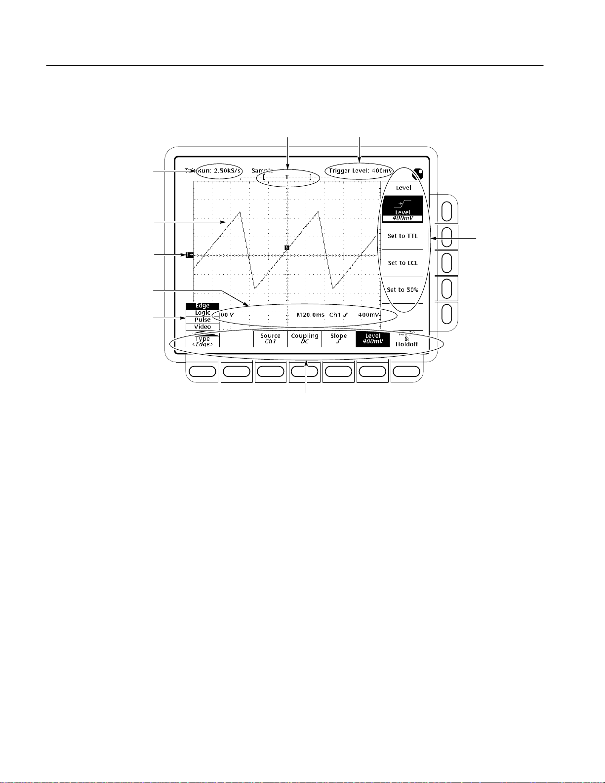
Operating Instructions
Brief status
information
Graticule and waveforms
Waveform reference
symbols shows ground
levels and waveform
sources
Vertical scale, horizontal scale,
and trigger level readouts
Pop-up menu
Position of waveform
record relative to
the screen and display
General purpose
knob readout
Side menu
area. Readouts
for
measurements
move here
when CLEAR
MENU is
pressed.
How to Use Help
How to Use the Status
Menu
Main menu display area. Readouts in lower graticule
area move here when CLEAR MENU is pressed.
Figure 2–1: Map of Display Functions
Push the HELP front-panel button to enter help mode. Front-panel knobs and
buttons now display information about their function when turned or pushed.
Push HELP again to exit help mode.
To get help information on a menu item, display the menu desired (if you are in
help mode, exit help first). Push HELP. Now the menu buttons display informa-
tion about their function when pushed.
Push the SHIFT, then the STATUS front-panel buttons to display the status
menu. You will find messages reflecting the state of the acquisition system,
whether it is running or stopped (and if it is stopped, why), as well as
setup-related information.
2–8
TDS 500B, TDS 600B and TDS 700A Service Manual

Operating Instructions
How to Set Functions
Special function controls.
Access all functions except
vertical, horizontal, and
trigger functions from this
front-panel control block.
Most functions can be set either by using one (or two) front-panel button(s) or
knob(s), or by pushing a front-panel button to use a main menu, and then a
side-menu button to set the function. The following steps illustrate both
procedures.
1. Locate the block that contains the function to be set.
Vertical function controls. Access all
vertical functions and inputs from
this front-panel control block.
Horizontal function controls.
Access all horizontal functions
from this front-panel block.
Trigger function controls.
Access all trigger functions
from this front-panel block.
TDS 500B, TDS 600B and TDS 700A Service Manual
2–9
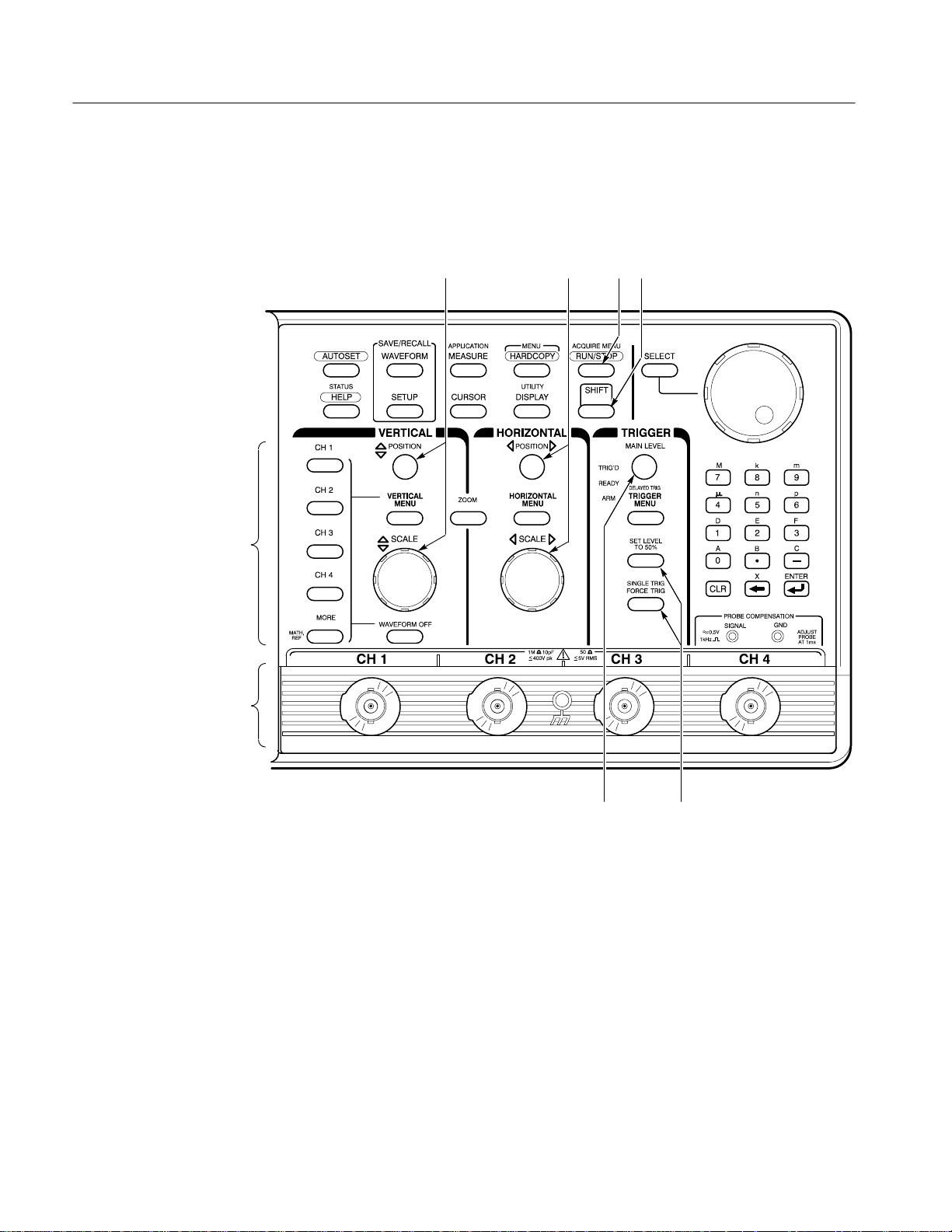
Operating Instructions
2. Select the waveform source(s). Position, scale, and set trigger level for
waveform source(s) directly from the front panel. The steps that follow
provide examples of possible control selections.
8
7
123
4
2–10
65
a. Input waveforms into these channels (7). Example: CH 1.
b. Push any channel’s button (8) to display its waveform. The last channel
turned on determines which waveform is positioned and scaled. The
indicator above the channel last selected is lighted.
Example: Push CH 1; then CH 2.
c. Vertically (1) and horizontally (2) scale and position the waveform(s)
selected. Example: Set the scale to 100 mV/div and center the waveform
on screen.
d. Stop and start acquiring waveforms (3). Example: Push RUN/STOP if
not acquiring.
TDS 500B, TDS 600B and TDS 700A Service Manual
Operating Instructions
e. Adjust trigger level (6) to trigger the waveform(s) selected or use these
buttons (5) to either set a trigger level at the mid-amplitude level of the
selected waveform or to force a single trigger. Example: Push SET
LEVEL TO 50%.
3. Set all other functions using menus.
a. Choose the waveform source (8) first if setting a vertical function; else
skip to step b. Example: Push CH 2.
b. Push SHIFT (4) if the function to be set is highlighted in blue; else skip
to step c.
9
14
13
10
11
12
c. Push the front-panel button that corresponds to the menu containing the
function. A main menu (14) for selecting among related functions
appears. Example: Push VERTICAL MENU.
Note the two labels: the top label is a function to choose from; the
bottom label tells you the current setting for that function. Offset is
currently set to 0 V.
d. Select a function from the main menu using the main-menu buttons (12).
A side menu for selecting among that the available settings for that
function appears. Example: Push Coupling (13).
TDS 500B, TDS 600B and TDS 700A Service Manual
2–11
Operating Instructions
e. Select the setting for the function from the side menu (9) using the
side-menu buttons (11). Example: Push AC (10).
How to Set Complex
Functions
18
A few functions require more than just two levels (main and side) of menus to
completely specify their settings. In such cases, either the main menu, the side
menu, or both are modified to supply additional choices. The procedures that
follow show both schemes.
1. Set up a function using pop-up menus:
15
17
16
a. For some selections, pushing a main-menu button pops up a menu (18)
of subfunctions. Example: Push Type (17).
Note the pop-up menu for Type is set to Edge. All the main-menu
buttons to the right of the pop-up menu are labeled with subfunctions of
Edge.
b. Pushing the button that popped up the menu (17) toggles through the
pop-up menu choices. Example: Repeatedly push Type to move through
the pop-up menu. Notice the other main-menu button labels change
accordingly. Push Type to move back to Edge.
c. Complete the setting of the desired mode by selecting from the main
menu and the side menu that results. Example: Push Mode & Holdoff
(16), and then push Normal (15).
2–12
TDS 500B, TDS 600B and TDS 700A Service Manual
Operating Instructions
2. Set up a function using the general purpose knob (20). (The examples of
possible menu selections in the substeps that follow assume you have pushed
TRIGGER MENU.)
19 20
21
a. Pushing some main-menu buttons displays a side menu with labels
containing readouts that can be varied. Example: Push Level (21).
b. Pushing the side-menu button Level assigns the general purpose knob to
control the readout appearing in the button label. It also copies the
readout to the general purpose knob readout area in the right corner of
the screen. Example: Push Level (19).
c. Use the general purpose knob (20) to adjust the trigger level to the
setting desired. Example: Turn the knob to –20 mV.
More About the General Purpose Knob. As you’ve just seen, the general purpose
knob can be used to extend the number of choices available to a side menu
button. The general purpose knob can also be assigned to control the following
functions:
H Cursor positioning
H Display intensities
H Delay time
TDS 500B, TDS 600B and TDS 700A Service Manual
2–13

Operating Instructions
H Gated measurements
H Number of events
H Template generation
H Trigger position
H Holdoff
H Offset
H Variable persistence
In all cases, the menus are used to select the function to which the general
purpose knob is assigned. The following attributes apply to this knob:
H Depending on the function it is assigned to control, the general purpose knob
may vary numerical readouts, position objects (cursors) on screen, or select
between icon-label settings that show up in side-menu labels.
H The general purpose knob has a readout area at the upper right corner of the
screen. (See Figure 2–1.) This readout always reflects the name and value of
the function that the general purpose knob is currently controlling.
H Whenever the general purpose knob assignment is changed, a knob icon
appears immediately to the left of the general purpose knob readout to notify
you of the assignment change. The icon is removed as soon as you use the
general purpose knob to change the value of the function it is assigned to.
H To assign the general purpose knob to control a function, display the menu
containing the function; then select the function. (Note that not all functions
can be controlled by the general purpose knob.)
H Whenever the menu is removed, the general purpose knob is not assigned
and doesn’t control any function. (An exception is the cursor function. If
cursors are turned on, removing the menu leaves the knob assigned to control
the cursors until reassigned by selecting another menu and function that uses
the knob.)
H When the SHIFT button is lighted, the general purpose knob becomes a
coarse adjustment. When the SHIFT button is not lighted, the general
purpose knob becomes a fine adjustment.
H The general purpose knob also has a SELECT button. This button is used to
toggle the knob between the control of either of the two cursors displayed
when H-bar or V-bar cursors are turned on in the cursor menu.
2–14
TDS 500B, TDS 600B and TDS 700A Service Manual

Operating Instructions
Display and Utility Menus. Using the techniques described for using menus, you
can access and change functions in the display menu and utilities menu. In the
Display menu, you can set the following functions:
H Color: waveforms, readouts, graticule
H Intensity: waveforms, readouts, graticule, etc.
H Style of waveform display(s): vectors or dots, intensified or nonintensified
samples, and infinite or variable persistence
H Display format: XY or YT
H Graticule format: type
H Waveform interpolation filter and readout options
From the Utility menu, you can configure the GPIB port (talk/listen, address,
etc.) and access internal routines for self diagnostics and self compensation.
Instructions for setting up communication over the GPIB are found in Section 5,
Adjustment Procedures.
TDS 500B, TDS 600B and TDS 700A Service Manual
2–15

Operating Instructions
2–16
TDS 500B, TDS 600B and TDS 700A Service Manual


Theory of Operation
This section describes the electrical operation of the TDS 500B, TDS 600B and
TDS 700A Digitizing Oscilloscopes using the major circuit blocks or modules.
This section has two main parts:
H Logic Conventions describes how logic functions are discussed and
represented in this manual.
H Module Overview describes circuit operation from a functional-circuit block
perspective.
Logic Conventions
The Digitizing Oscilloscopes contain many digital logic circuits. This manual
refers to these circuits with standard logic symbols and terms. Unless otherwise
stated, all logic functions are described using the positive-logic convention: the
more positive of the two logic levels is the high (1) state, and the more negative
level is the low (0) state. Signal states may also be described as “true” meaning
their active state or “false” meaning their nonactive state. The specific voltages
that constitute a high or low state vary among the electronic devices.
Module Overview
General
Input Signal Path
Active-low signals are indicated by a tilde prefixed to the signal name (~RESET). Signal names are considered to be either active-high, active-low, or to have
both active-high and active-low states.
This module overview describes the basic operation of each functional circuit
block as shown in Figure 9-2.
The TDS 500B, TDS 600B and TDS 700A Digitizing Oscilloscopes have four
channels. Each channel provides a calibrated vertical scale factor.
A signal enters the oscilloscope through a probe connected to a BNC on the A10
Attenuator/Acquisition board.
Attenuators. Circuitry in the attenuator selects the input coupling, termination,
and the attenuation factor. The processor system, by way of the acquisition
system, controls the attenuators. For example, if 50 W input termination is
TDS 500B, TDS 600B and TDS 700A Service Manual
3–1

Theory of Operation
selected and the input is overloaded, the processor system switches the input to
the 1 MW position.
Probe Coding Interface. Probe coding interface signals pass through the attenuator
portion of the A10 Attenuator/Acquisition to the acquisition system, where they
are sensed and controlled.
Acquisition System. The acquisition system amplifies the input signals, samples
them, converts them to digital signals, and controls the acquisition process under
direction of the processor system. The acquisition system includes the trigger,
acquisition timing, and acquisition mode generation and control circuitry.
V oltage Controlled Oscillator (VCO). Master clocks for the acquisition system are
generated by the circuitry on the A10 Acquisition board. The circuitry makes up
a phase-locked loop. The master clock is divided down by the A10 Acquisition
circuitry under control of the processor system.
D1 Bus. The acquisition system passes the digital values representing the
acquired waveform through the A14 D1 Bus to the A11 DRAM Processor/Display board. This happens after a waveform acquisition is complete if the digital
signal processor in the processor system requests the waveform.
Processor System. The processor system contains a 68020 microprocessor that
controls the entire instrument. This system also includes the firmware and a
GPIB interface. You can reprogram the firmware from a remote controller using
the GPIB and an external software package.
The processor also includes a digital signal processor. This signal processor
processes each waveform as directed by the system processor. Waveforms and
any text to be displayed are passed on to the display system. The A11 DRAM
Processor/Display board contains both the processor and display systems.
Display System. Text and waveforms are processed by different parts of the
display circuitry. The display system sends the text and waveform information to
the tube assembly as a video signal. The display system also generates and sends
vertical (VSYNC) and horizontal (HSYNC) sync signals to the tube assembly. A
VGA-compatible video output is at the rear of the TDS 500B, TDS 600B and
TDS 700A.
3–2
Tube Assembly
All information (waveforms, text, graticules, and pictographs) is displayed by the
A30/31/32 Display system. The A30 generates the high voltages necessary to
drive the display tube. It also contains the video amplifier, horizontal oscillator,
and the vertical and horizontal yoke driver circuitry.
TDS 500B, TDS 600B and TDS 700A Service Manual

Theory of Operation
Front Panel
Rear Panel
Low Voltage Power
Supply
The processor system sends instructions to and receives information from the
Front Panel Processor on the A12 Front Panel board. The Front Panel Processor
reads the front-panel switches and potentiometers. Any changes in their settings
are reported to the processor system. The Front Panel Processor also turns the
LEDs on and off and generates the bell signal.
Front-panel menu switches are also read by the Front Panel Processor. The
processor sends any changes in menu selections to the processor system. The
ON/STBY switch is one of the menu switches. However, it is not read by the
Front Panel Processor, but passes through the A12 Front Panel board and the A11
DRAM Processor/Display board to the low voltage power supply.
The front panel also generates the probe compensation signals SIGNAL
and GND.
The GPIB connector provides access to stored waveforms and allows external
control of the oscilloscope.
You can make hardcopies on the GPIB, RS-232 and Centronics ports.
The low voltage power supply is a switching power converter with active power
factor control. It supplies power to all of the circuitry in the oscilloscope.
Fan
The principal POWER switch, located on the rear panel, controls all power to
the oscilloscope including the Low Voltage Power Supply. The ON/STBY
switch, located on the front panel, also controls all of the power to the oscilloscope except for part of the circuitry in the Low Voltage Power Supply.
The power supply sends a power fail (~PF) warning to the processor system if
the power is going down.
The fan provides forced air cooling for the oscilloscope. It connects to +25 V
from the Low Voltage Power Supply by way of the A11 DRAM Processor/Display module.
TDS 500B, TDS 600B and TDS 700A Service Manual
3–3

Theory of Operation
3–4
TDS 500B, TDS 600B and TDS 700A Service Manual


Performance Verification Procedures
Two types of Performance Verification procedures can be performed on this
product; Brief Procedures and Performance Tests. You may not need to perform
all of these procedures, depending on what you want to accomplish.
H To rapidly confirm that the oscilloscope functions and was adjusted properly,
just do the brief procedures under Self Tests, which begin on page 4–5.
Advantages: These procedures are quick to do, require no external equip-
ment or signal sources, and perform extensive functional and accuracy
testing to provide high confidence that the oscilloscope will perform
properly. They can be used as a quick check before making a series of
important measurements.
H To further check functionality, first do the Self Tests just mentioned; then do
the brief procedures under Functional Tests that begin on page 4–7.
Advantages: These procedures require minimal additional time to perform,
require no additional equipment other than a standard-accessory probe, and
more completely test the internal hardware of the oscilloscope. They can be
used to quickly determine if the oscilloscope is suitable for putting into
service, such as when it is first received.
H If more extensive confirmation of performance is desired, do the Perfor-
mance Tests, beginning on page 4–15, after doing the Functional and Self
Tests just referenced.
Advantages: These procedures add direct checking of warranted specifications. They require more time to perform and suitable test equipment is
required. (See Equipment Required beginning on page 4–16.)
If you are not familiar with operating this oscilloscope, read the TDS 500B,
TDS 600B & TDS 700A Reference (070-9382-XX) or the TDS 500B, TDS 600B
& TDS 700A User Manual (070-9719-XX). These contain instructions that will
acquaint you with the use of the front-panel controls and the menu system.
TDS 500B, TDS 600B and TDS 700A Service Manual
4–1

Performance Verification Procedures
Input Channels vs. Model
When performing the procedures in this section, be aware that some TDS models
refer to input channels Ch 3 and Ch 4 as Aux 1 and Aux 2 respectively. Where
appropriate, both names will appear in the procedure, for example, Ch 3 (Aux 1).
The channel names for the various TDS models are shown below.
TDS Model Channel Names
Conventions
TDS 540B, 644B, 684B, 754A, and 784A
TDS 520B, 620B, 680B, 724A, and 782A Ch 1, Ch 2, Aux 1, and Aux 2
Throughout these procedures the following conventions apply:
H Each test procedure uses the following general format:
Title of Test
Equipment Required
Prerequisites
Procedure
H Each procedure consists of as many steps, substeps, and subparts as required
to do the test. Steps, substeps, and subparts are sequenced as follows:
1. First Step
Ch 1, Ch 2, Ch 3, and Ch 4
4–2
a. First Substep
H First Subpart
H Second Subpart
b. Second Substep
2. Second Step
H In steps and substeps, the lead-in statement in italics instructs you what to do,
while the instructions that follow tell you how to do it, as in the example
step below, “Initialize the oscilloscope” by doing “Press save/recall SETUP.
Now, press the main-menu button...”.
TDS 500B, TDS 600B and TDS 700A Service Manual
Performance Verification Procedures
Initialize the oscilloscope: Press save/recall SETUP. Now, press the
main-menu button Recall Factory Setup; then the side-menu button OK
Confirm Factory Init.
H Where instructed to use a front-panel button or knob, or select from a main
or side menu, or verify a readout or status message, the name of the button or
knob appears in boldface type: “press SHIFT; then UTILITY, press the
main-menu button System until Cal is highlighted in the pop-up menu.
Verify that the status message is Pass in the main menu under the Voltage
Reference label.”
STOP. The symbol at the left is accompanied by information you must read to do
the procedure properly.
H Refer to Figure 4–1: “Main menu” refers to the menu that labels the seven
menu buttons under the display; “side menu” refers to the menu that labels
the five buttons to the right of the display. “Pop-up menu” refers to a menu
that pops up when a main-menu button is pressed.
Brief status
information
Graticule and waveforms
Waveform reference
symbols show ground levels
and waveform sources
Vertical scale, horizontal scale,
and trigger level readouts
Pop-up menu
Position of waveform
record relative to
the screen and display
General purpose
knob readout
Side menu
area. Readouts
for
measurements
move here
when CLEAR
MENU is
pressed.
Main menu display area. Readouts in lower graticule
area move here when CLEAR MENU is pressed.
Figure 4–1: Map of Display Functions
TDS 500B, TDS 600B and TDS 700A Service Manual
4–3

Performance Verification Procedures
4–4
TDS 500B, TDS 600B and TDS 700A Service Manual

Brief Procedures
Self Tests
The Self Tests use internal routines to confirm basic functionality and proper
adjustment. No test equipment is required to do these test procedures.
The Functional Tests utilize the probe-compensation output at the front panel as a
test-signal source for further verifying that the oscilloscope functions properly. A
probe, such as the P6243 or P6245, is required to do these test procedures.
This procedure uses internal routines to verify that the oscilloscope functions and
was adjusted properly. No test equipment or hookups are required.
Verify Internal
Adjustment, Self
Compensation, and
Diagnostics
Equipment Required
Prerequisites Power on the Digitizing Oscilloscope and allow a 20 minute warm-up
1. Verify that internal diagnostics pass: Do the following substeps to verify
passing of internal diagnostics.
a. Display the System diagnostics menu:
H Press SHIFT; then press UTILITY.
H Repeatedly press the main-menu button System until Diag/Err is
highlighted in the pop-up menu.
b. Run the System Diagnostics:
H First disconnect any input signals from all four channels.
H Press the main-menu button Execute; then press the side-menu
button OK Confirm Run Test.
c. Wait: The internal diagnostics do an exhaustive verification of proper
oscilloscope function. This verification will take up to three and a half
minutes on some models. At some time during the wait, a “clock” icon
(shown at left) will appear on-screen. When the verification is finished,
the resulting status will appear on the screen.
None
before doing this procedure.
d. Confirm no failures are found: Verify that no failures are found and
reported on-screen.
TDS 500B, TDS 600B and TDS 700A Service Manual
4–5
Brief Procedures
e. Confirm the three adjustment sections have passed status:
H Press SHIFT; then press UTILITY.
H Highlight Cal in the pop-up menu by repeatedly pressing the
main-menu button System. See Figure 4–2.
H Verify that the word Pass appears in the main menu under the
following menu labels: Voltage Reference, Frequency Response,
and Pulse Trigger. See Figure 4–2.
f. Run the signal-path compensation: Press the main-menu button Signal
Path; then press the side-menu button OK Compensate Signal Paths.
g. Wait: Signal-path compensation may take five minutes on the
TDS 500B/700A and fifteen minutes on the 600B to run. While it
progresses, a “clock” icon (shown at left) is displayed on-screen. When
compensation completes, the status message will be updated to Pass or
Fail in the main menu. See step h.
h. Confirm signal-path compensation returns passed status: Verify that the
word Pass appears under Signal Path in the main menu. See Figure 4–2.
4–6
Highlight Cal
1
3
Verify Pass
2
Verify Pass
Figure 4–2: Verifying Adjustments and Signal-Path Compensation
TDS 500B, TDS 600B and TDS 700A Service Manual

Functional Tests
Brief Procedures
2. Return to regular service: Press CLEAR MENU to exit the system menus.
The purpose of these procedures is to confirm that the oscilloscope functions
properly. The only equipment required is one of the standard-accessory probes
and, to check the file system, a 3.5 inch, 720 K or 1.44 Mbyte floppy disk.
CAUTION. The optional P6243 and P6245 probes that can be used with this
oscilloscope provide an extremely low loading capacitance (<1 pF) to ensure the
best possible signal reproduction. These probes should not be used to measure
signals exceeding ±8 volts, or errors in signal measurement will be observed.
Above 40 volts, damage to the probe may result. To make measurements beyond
±10 volts, use either the P6139A probe (good to 500 volts), or refer to the
catalog for a recommended probe.
STOP. These procedures verify functions; that is, they verify that the oscilloscope
features operate. They do not verify that they operate within limits.
Therefore, when the instructions in the functional tests that follow call for you to
verify that a signal appears on-screen “that is about five divisions in amplitude”
or “has a period of about six horizontal divisions,” etc., do NOT interpret the
quantities given as limits. Operation within limits is checked in Performance
Tests, which begin on page 4–15.
STOP. DO NOT make changes to the front-panel settings that are not called out
in the procedures. Each verification procedure will require you to set the
oscilloscope to certain default settings before verifying functions. If you make
changes to these settings, other than those called out in the procedure, you may
obtain invalid results. In this case, just redo the procedure from step 1.
When you are instructed to press a menu button, the button may already be
selected (its label will be highlighted). If this is the case, it is not necessary to
press the button.
TDS 500B, TDS 600B and TDS 700A Service Manual
4–7
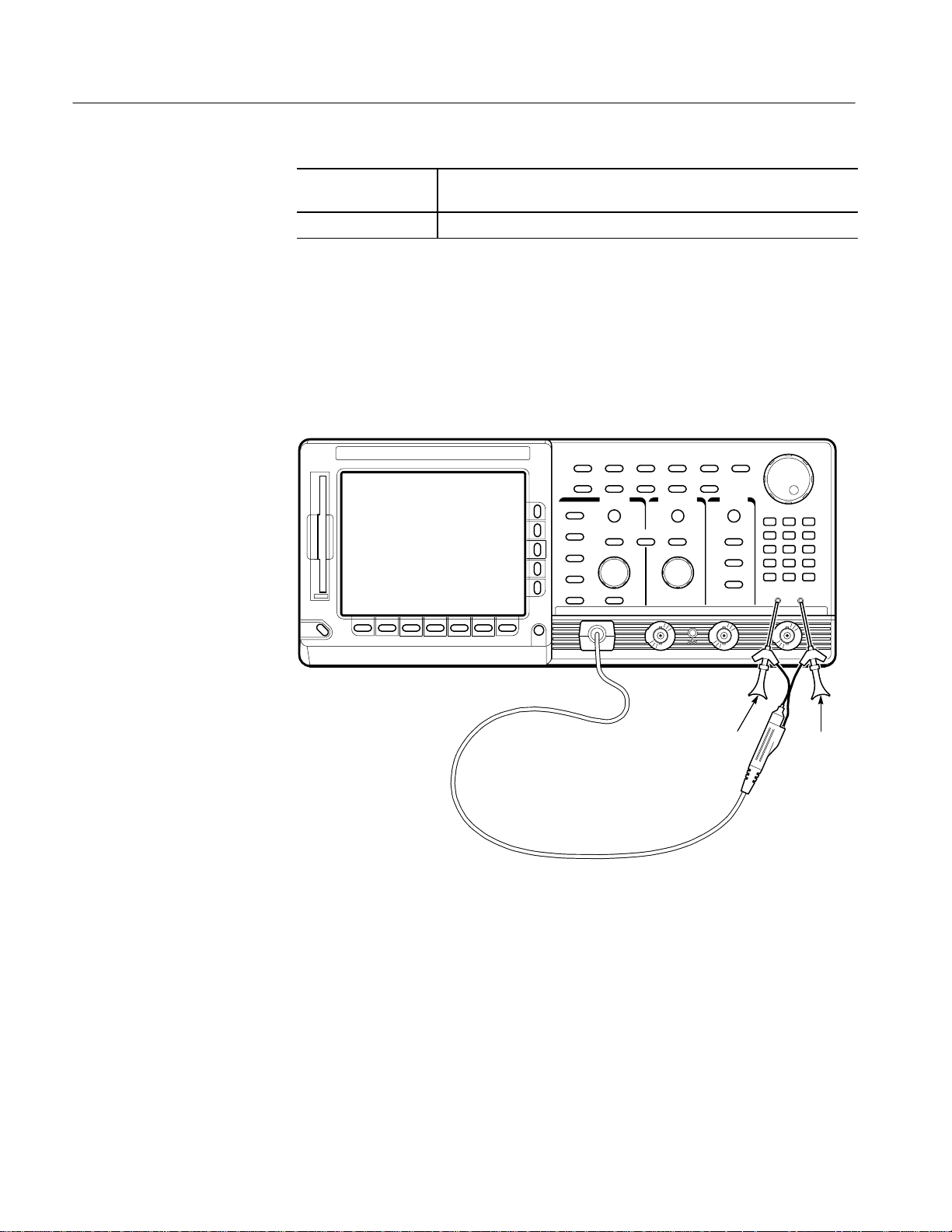
Brief Procedures
Verify All Input Channels
Equipment Required
Prerequisites None
One probe such as the P6243, P6245 or P6139A
1. Install the test hookup and preset the oscilloscope controls:
a. Hook up the signal source: Install the probe on CH 1. Connect the probe
tip to PROBE COMPENSATION SIGNAL on the front panel; connect
the probe ground (typically black) to PROBE COMPENSATION
GND. If using a P6243 or P6245 probe, you may want to attach a Y-lead
connector and two SMD KlipChips as shown in Figure 4–3.
4–8
Signal Gnd
Figure 4–3: Universal Test Hookup for Functional Tests – TDS 600B Shown
b. Initialize the oscilloscope:
H Press save/recall SETUP.
H Press the main-menu button Recall Factory Setup.
H Press the side-menu button OK Confirm Factory Init.
TDS 500B, TDS 600B and TDS 700A Service Manual

Brief Procedures
2. Verify that all channels operate: Do the following substeps — test CH 1 first,
skipping substep a and b since CH 1 is already set up for verification and as
the trigger source from step 1.
a. Select an unverified channel:
H Press WAVEFORM OFF to remove the channel just verified from
display.
H Press the front-panel button that corresponds to the channel you are
to verify.
H Move the probe to the channel you selected.
b. Match the trigger source to the channel selected:
H Press TRIGGER MENU.
H Press the main-menu button Source.
H Press the side-menu button that corresponds to the channel selected,
Ch2, Ch3, or Ch4. (Some TDS models use Ax1 and Ax2 instead of
Ch3 and Ch4).
c. Set up the selected channel:
H Set the vertical SCALE to 200 mV.
H Set the horizontal SCALE to 200 ms. Press CLEAR MENU to
remove any menu that may be on the screen.
d. Verify that the channel is operational: Confirm that the following
statements are true.
H The vertical scale readout for the channel under test shows a setting
of 200 mV, and a square-wave probe-compensation signal about
2.5 divisions in amplitude is on-screen. See Figure 4–1 on page 4–3
to locate the readout.
H The vertical POSITION knob moves the signal up and down the
screen when rotated.
H Turning the vertical SCALE knob counterclockwise decreases the
amplitude of the waveform on-screen, turning the knob clockwise
increases the amplitude, and returning the knob to 200 mV returns
the amplitude to about 2.5 divisions.
e. Verify that the channel acquires in all acquisition modes: Press SHIFT;
then press ACQUIRE MENU. Use the side menu to select, in turn, each
of the three hardware acquire modes and confirm that the following
statements are true. Refer to the icons at the left of each statement as you
confirm those statements.
TDS 500B, TDS 600B and TDS 700A Service Manual
4–9

Brief Procedures
H Sample mode displays an actively acquiring waveform on-screen.
(Note that there is noise present on the peaks of the square wave.)
H Peak Detect mode displays an actively acquiring waveform
on-screen with the noise present in Sample mode “peak detected.”
H Hi Res mode (TDS 500B and 700A only) displays an actively
acquiring waveform on-screen with the noise that was present in
Sample mode reduced.
H Envelope mode displays an actively acquiring waveform on-screen
with the noise displayed.
H Average mode displays an actively acquiring waveform on-screen
with the noise reduced.
f. Test all channels: Repeat substeps a through e until all four input
channels are verified.
3. Remove the test hookup: Disconnect the probe from the channel input and the
probe-compensation terminals.
Verify the Time Base
Equipment Required
Prerequisites None
One probe such as the P6243, P6245 or P6139A
1. Install the test hookup and preset the oscilloscope controls:
a. Hook up the signal source: Install the probe on CH 1. Connect the probe
tip to PROBE COMPENSATION SIGNAL on the front panel; connect
the probe ground to PROBE COMPENSATION GND. See Figure 4–3
on page 4–8.
b. Initialize the oscilloscope:
H Press save/recall SETUP.
H Press the main-menu button Recall Factory Setup; then press the
side-menu button OK Confirm Factory Init.
c. Modify default settings:
H Set the vertical SCALE to 200 mV.
H Set the horizontal SCALE to 200 ms.
4–10
H Press CLEAR MENU to remove the menus from the screen.
2. Verify that the time base operates: Confirm the following statements.
TDS 500B, TDS 600B and TDS 700A Service Manual

Brief Procedures
a. One period of the square-wave probe-compensation signal is about five
horizontal divisions on-screen for the 200 ms horizontal scale setting (set
in step 1c).
b. Rotating the horizontal SCALE knob clockwise expands the waveform
on-screen (more horizontal divisions per waveform period), counterclockwise rotation contracts it, and returning the horizontal scale to
200 ms returns the period to about five divisions.
c. The horizontal POSITION knob positions the signal left and right
on-screen when rotated.
3. Remove the test hookup: Disconnect the probe from the channel input and the
probe-compensation terminals.
Verify the Main and
Delayed Trigger Systems
Equipment Required
Prerequisites None
One probe such as the P6243, P6245, or P6139A
1. Install the test hookup and preset the oscilloscope controls:
a. Hook up the signal source: Install the probe on CH 1. Connect the probe
tip to PROBE COMPENSATION SIGNAL on the front panel; connect
the probe ground to PROBE COMPENSATION GND. See Figure 4–3
on page 4–8.
b. Initialize the oscilloscope:
H Press save/recall SETUP.
H Press the main-menu button Recall Factory Setup.
H Press the side-menu button OK Confirm Factory Init.
c. Modify default settings:
H Set the vertical SCALE to 200 mV.
H Set the horizontal SCALE for the M (main) time base to 200 ms.
H Press TRIGGER MENU.
H Press the main-menu button Mode & Holdoff.
H Press the side-menu button Normal.
H Press CLEAR MENU to remove the menus from the screen.
TDS 500B, TDS 600B and TDS 700A Service Manual
4–11

Brief Procedures
2. Verify that the main trigger system operates: Confirm that the following
statements are true.
H The trigger level readout for the main trigger system changes with the
trigger-LEVEL knob.
H The trigger-LEVEL knob can trigger and untrigger the square-wave
signal as you rotate it. (Leave the signal untriggered, which is indicated
by the display not updating.)
H Pressing SET LEVEL TO 50% triggers the signal that you just left
untriggered. (Leave the signal triggered.)
3. Verify that the delayed trigger system operates:
a. Select the delayed time base:
H Press HORIZONTAL MENU.
H Press the main-menu button Time Base.
H Press the side-menu button Delayed Triggerable; then press the
side-menu button Delayed Only.
H Set the horizontal SCALE for the D (delayed) time base to 200 ms.
b. Select the delayed trigger level menu:
H Press SHIFT; then press DELAYED TRIG.
H Press the main-menu button Level; then press the side-menu button
Level.
c. Confirm that the following statements are true:
H The trigger-level readout for the delayed trigger system changes as
you turn the general purpose knob.
H As you rotate the general purpose knob, the square-wave probe-com-
pensation signal can become triggered and untriggered. (Leave the
signal untriggered, which is indicated by the display not updating.)
H Pressing the side-menu button Set to 50% triggers the probe-com-
pensation signal that you just left untriggered. (Leave the signal
triggered.)
d. Verify the delayed trigger counter:
4–12
H Press the main-menu button Delay by Time.
H Use the keypad to enter a delay time of 1 second. Press 1, then press
ENTER.
TDS 500B, TDS 600B and TDS 700A Service Manual

Brief Procedures
H Verify that the trigger READY indicator on the front panel flashes
about once every second as the waveform is updated on-screen.
4. Remove the test hookup: Disconnect the probe from the channel input and the
probe-compensation terminals.
Verify the File System
Equipment Required
Prerequisites None
One probe such as the P6243, P6245 or P6139A
One 720 K or 1.44 Mbyte, 3.5 inch DOS-compatible disk.
You can use a disk of your own or you can use the Programming
Examples Software 3.5 inch disk (Tektronix part number 063-1 134-XX)
contained in the TDS Family Programmer Manual (Tektronix part
number 070-9556-XX).
1. Install the test hookup and preset the oscilloscope controls:
a. Hook up the signal source: Install the probe on CH 1. Connect the probe
tip to PROBE COMPENSATION SIGNAL on the front panel; connect
the probe ground to PROBE COMPENSATION GND. See Figure 4–3
on page 4–8.
b. Insert the test disk: Insert the disk in the disk drive to the left of the
monitor.
H Position the disk so the metal shutter faces the drive.
H Position the disk so the stamped arrow is on the top right side. In
other words, place the angled corner in the front bottom location.
H Push the disk into the drive until it goes all the way in and clicks into
place.
c. Initialize the oscilloscope:
H Press save/recall SETUP.
H Press the main-menu button Recall Factory Setup.
H Press the side-menu button OK Confirm Factory Init.
d. Modify default settings:
H Set the vertical SCALE to 200 mV.
H Set the horizontal SCALE for the M (main) time base to 200 ms.
Notice the waveform on the display now shows two cycles instead of
five.
H Press CLEAR MENU to remove the menus from the screen.
TDS 500B, TDS 600B and TDS 700A Service Manual
4–13

Brief Procedures
e. Save the settings:
H Press SETUP.
H Press the main-menu button Save Current Setup; then press the
side-menu button To File.
H Turn the general purpose knob to select the file to save. Choose
(or ). With this choice, you will save a file
starting with , then containing 5-numbers, and a extension.
For example, the first time you run this on a blank, formatted disk or
on the Example Programs Disk, the oscilloscope will assign the
name to your file. If you ran the procedure again, the
oscilloscope would increment the name and call the file
.
H Press the side-menu button Save To Selected File.
2. Verify the file system works:
H Press the main-menu button Recall Factory Setup and the side-menu
button OK Confirm Factory Init to restore the 500 ms time base and the
five cycle waveform.
H Press the main-menu button Recall Saved Setup; then press the
side-menu button From File.
H Turn the general purpose knob to select the file to recall. For example, if
you followed the instructions above and used a blank disk, you had the
oscilloscope assign the name TEK00000.SET to your file.
H Press the side-menu button Recall From Selected File.
H Verify that Digitizing Oscilloscope retrieved the saved setup from the
disk. Do this by noticing the horizontal SCALE for the M (main) time
base is again 200 ms and the waveform shows only two cycles just as it
was when you saved the setup.
3. Remove the test hookup:
H Disconnect the probe from the channel input and the probe-compensation
terminals.
H Remove the disk from the disk drive. Do this by pushing in the tab at the
bottom of the disk drive.
4–14
TDS 500B, TDS 600B and TDS 700A Service Manual

Performance Tests
This section contains a collection of procedures for checking that the TDS 500B,
TDS 600B, and TDS 700A Digitizing Oscilloscopes perform as warranted.
The procedures are arranged in four logical groupings: Signal Acquisition System
Checks, Time Base System Checks, Triggering System Checks, and Output Ports
Checks. They check all the characteristics that are designated as checked in
Specifications. (The characteristics that are checked appear in boldface type
under Warranted Characteristics in Specifications.)
STOP. These procedures extend the confidence level provided by the basic
procedures described on page 4–5. The basic procedures should be done first,
then these procedures performed if desired.
Prerequisites
The tests in this section comprise an extensive, valid confirmation of performance and functionality when the following requirements are met:
H The cabinet must be installed on the Digitizing Oscilloscope.
H You must have performed and passed the procedures under Self Tests, found
on page 4–5, and those under Functional Tests, found on page 4–7.
H A signal-path compensation must have been done within the recommended
calibration interval and at a temperature within ±5_ C of the present
operating temperature. (If at the time you did the prerequisite Self Tests, the
temperature was within the limits just stated, consider this prerequisite met.)
H The Digitizing Oscilloscope must have been last adjusted at an ambient
temperature between +20_ C and +30_ C, must have been operating for a
warm-up period of at least 20 minutes, and must be operating at an ambient
temperature between +4_ C and either +45_ C for the TDS 600B or +50_ C
for the TDS 500B and 700A. (The warm-up requirement is usually met in the
course of meeting the Self Tests and Functional Tests prerequisites listed
above.)
TDS 500B, TDS 600B and TDS 700A Service Manual
4–15

Performance Tests
Equipment Required
These procedures use external, traceable signal sources to directly check
warranted characteristics. The required equipment list follows this introduction.
T able 4–1: Test Equipment
Item Number and
Description
1. Attenuator ,10X
(two required)
2. Attenuator , 5X
3. Adapter, BNC female to
Clip Leads
4. Terminator, 50 Impedance 50 ; connectors: female
5. Cable, Precision 50
Coaxial (two required)
6. Connector , Dual-Banana
(two required)
7. Connector , BNC “T” Male BNC to dual female BNC T ektronix part number
8. Coupler, Dual-Input Female BNC to dual male BNC Tektronix part number
9. Generator , DC Calibration
10. Generator, Calibration 500 mV square wave calibrator
11. Generator, Time Mark Variable marker frequency from 10 ms
12. Probe, 10X A P6139A, P6243, or P6245 probe
13. 3.5 inch, 720 K or
1.44 Mbyte, DOS-compatible floppy disk
14. Generator, Video Signal Provides PAL compatible outputs Tektronix TSG 121 Used to Test Video Option 05
Minimum Requirements Example Purpose
Ratio: 10X; impedance 50 ; connectors: female BNC input, male BNC
output
Ratio: 5X; impedance 50 ; connectors: female BNC input, male BNC
output
BNC female to Clip Leads Tektronix part number
BNC input, male BNC output
50 , 36 in, male to male BNC
connectors
Female BNC to dual banana Tektronix part number
Variable amplitude to ±104 V; accuracy to 0.1%
amplitude; accuracy to 0.25%
to 10 ns; accuracy within 2 ppm
Tektronix part number
01 1-0059-02
Tektronix part number
01 1-0060-02
013-0076-00
Tektronix part number
01 1-0049-01
Tektronix part number
012-0482-00
103-0090-00
103-0030-00
067-0525-02
Data Precision 8200 Checking DC Offset, Gain,
Wavetek 9100 with options
100 and 250 (or, optionally,
Tektronix PG 506A Calibration
Generator
Wavetek 9100 with options
100 and 250 (or, optionally,
Tektronix TG 501A Time
Mark Generator
2
Tektronix part number P6139A
or P6245
Programming Examples
Software Disk (Tektronix part
number 063-1134-XX) that
comes with the TDS Family
Programmer Manual (Tektronix part number 070-9556-XX)
1
)
1)
Signal Attenuation
Signal Attenuation
Signal Coupling for Probe
Compensator Output Check
Signal Termination for
Channel Delay Test
Signal Interconnection
Various Accuracy Tests
Checking Trigger Sensitivity
Checking Delay Between
Channels
and Measurement Accuracy
To check accuracy of CH 3
Signal Out
Checking Sample-Rate and
Delay-time Accuracy
Signal Interconnection
Checking File System Basic
Functionality
Equipped Instruments Only
4–16
TDS 500B, TDS 600B and TDS 700A Service Manual

Performance Tests
T able 4–1: Test Equipment (Cont.)
Item Number and
Description
15. Oscillator, Leveled Sine
wave Generator
60 Hz Sine wave Wavetek 9100 with options
100 and 250 (or, optionally,
Tektronix SG 502)
16. Pulse Generator Tektronix CFG280
(or, optionally, PG 502)
17. Cable, Coaxial
(two required)
18. Terminator, 75
(two required)
75 , 36 in, male to male BNC
connectors
Impedance 75 ; connectors: female
BNC input, male BNC output
19. Generator, Sine Wave 100 kHz to at least 400 MHz. V ariable
amplitude from 12 mV to 2 V
p-p
.
Tektronix part number
012-1338-00
Tektronix part number
01 1-0102-01
Rohde & Schwarz SMY
3
Frequency accuracy >2.0%
20. Meter, Level and Power
Sensor
21. Splitter, Power Frequency range: DC to 1 GHz.
Frequency range:10 MHz to 400MHz.
Amplitude range: 6 mVp-p to 2 V
p-p
Rohde & Schwarz URV 35,
with NRV-Z8 power sensor
Rohde & Schwarz RVZ
3
Tracking: >2.0%
22. Generator, Function Frequency range 5 MHz to 10 MHz.
T ektronix CFG280 Checking External Clock
Square wave transition time 25 ns.
Amplitude range: 0 to 10 V
p-p
into 50
23. Adapter (four required) Male N to female BNC Tektronix 103–0045–00 Checking Analog Bandwidth
24. Adapter Female N to male BNC T ektronix 103–0058–00 Checking Analog Bandwidth
25. Generator,
Leveled Sine Wave,
200 kHz to 250 MHz; Variable amplitude from 5 mV to 4 V
into 50
p-p
Tektronix SG 503 Leveled
Sine Wave Generator
1, 3
Medium-Frequency
(optional)
26. Generator, Leveled Sine
Wave, High-Frequency
(optional)
1
Requires a TM 500 or TM 5000 Series Power Module Mainframe.
2
Warning: The optional P6243 and P6245 probes that may be used with this oscilloscope provide an extremely low loading
250 MHz to 1 GHz; Variable amplitude
from 500 mV to 4 V
into 50 ;
p-p
6 MHz reference
Tektronix SG 504 Leveled
Sine Wave Generator
SG 504 Output Head
1
with
3
capacitance (<1 pF) to ensure the best possible signal reproduction. These probes should not be used to measure signals
exceeding ±8 V, or errors in signal measurement will be observed. Above 40 V, damage to the probe may result. To make
measurements beyond ±8 V , use either the P6139A probe (good to 500 V), or refer to the catalog for a recommended probe.
3
You can replace items 19, 20, or 21 with a Tektronix SG503 (item 25) or SG504 (item 26) – if available.
PurposeExampleMinimum Requirements
Used to Test Video Option 05
Equipped Instruments Only
Used to Test Video Option 05
Equipped Instruments Only
Used to Test Video Option 05
Equipped Instruments Only
Used to Test Video Option 05
Equipped Instruments Only
Checking Analog Bandwidth,
Trigger Sensitivity , Samplerate, External Clock, and
Delay-Time Accuracy
Checking Analog Bandwidth
3
and Trigger Sensitivity
Checking Analog Bandwidth
Checking Trigger Sensitivity at
low frequencies
Checking Analog Bandwidth
and Trigger Sensitivity at high
frequencies
TDS 500B, TDS 600B and TDS 700A Service Manual
4–17

Performance Tests
4–18
TDS 500B, TDS 600B and TDS 700A Service Manual

Performance Tests
TDS 600B Test Record
Photocopy this and the next three pages and use them to record the performance
test results for your TDS 600B.
TDS 600B T est Record
Instrument Serial Number: Certificate Number:
Temperature: RH %:
Date of Calibration: Technician:
TDS 600B Performance Test Minimum Incoming Outgoing Maximum
Offset Accuracy
CH1 Offset +1 mV
+101 mV
+1.01 V
CH2 Offset +1 mV
+101 mV
+1.01 V
CH3 or AX1 +1 mV
Offset +101 mV
+1.01 V
CH4 or AX2 +1 mV
Offset +101 mV
+1.01 V
DC Voltage Measurement Accuracy (Averaged)
CH1 5 mV Vert scale setting,
–5 Div position setting, +1 V offset
CH1 5 mV Vert scale setting,
+5 Div position setting, –1 V offset
CH1 200 mV Vert scale setting,
–5 Div position setting, +10 V offset
CH1 200 mV Vert scale setting,
+5 Div position setting, –10 V offset
CH1 1 V Vert scale setting,
–5 Div position setting, +10 V offset
CH1 1 V Vert scale setting,
+5 Div position setting, –10 V offset
CH2 5 mV Vert scale setting,
–5 Div position setting, +1 V offset
CH2 5 mV Vert scale setting,
+5 Div position setting, –1 V offset
CH2 200 mV Vert scale setting,
–5 Div position setting, +10 V offset
CH2 200 mV Vert scale setting,
+5 Div position setting, –10 V offset
– 1.45 mV
– 69.1 mV
– 691 mV
– 1.45 mV
– 69.1 mV
– 691 mV
– 1.45 mV
– 69.1 mV
– 691 mV
– 1.45 mV
– 69.1 mV
– 691 mV
+ 1.0329 V __________ __________ + 1.0471 V
– 1.0471 V __________ __________ – 1.0329V
+ 11.4165 V __________ __________ + 11.7835 V
– 11.7835 V __________ __________ – 1 1.4165 V
+ 17.2425 V __________ __________ + 18.7575 V
– 18.7575 V __________ __________ – 17.2425 V
+ 1.0329 V __________ __________ + 1.0471 V
– 1.0471 V __________ __________ – 1.0329V
+ 11.4165 V __________ __________ + 11.7835 V
– 11.7835 V __________ __________ – 1 1.4165 V
__________
__________
__________
__________
__________
__________
__________
__________
__________
__________
__________
__________
__________
__________
__________
__________
__________
__________
__________
__________
__________
__________
__________
__________
+ 1.45 mV
+ 69.1 mV
+ 691 mV
+ 1.45 mV
+ 69.1 mV
+ 691 mV
+ 1.45 mV
+ 69.1 mV
+ 691 mV
+ 1.45 mV
+ 69.1 mV
+ 691 mV
TDS 500B, TDS 600B and TDS 700A Service Manual
4–19

Performance Tests
TDS 600B T est Record (Cont.)
Instrument Serial Number: Certificate Number:
Temperature: RH %:
Date of Calibration: Technician:
TDS 600B Performance Test MaximumOutgoingIncomingMinimum
CH2 1 V Vert scale setting,
–5 Div position setting, +10 V offset
CH2 1 V Vert scale setting,
+5 Div position setting, –10 V offset
CH3 5 mV Vert scale setting,
or AX1 –5 Div position setting, +1 V offset
CH3 5 mV Vert scale setting,
or AX1 +5 Div position setting, –1 V offset
CH3 200 mV Vert scale setting,
or AX1 –5 Div position setting, +10 V offset
CH3 200 mV Vert scale setting,
or AX1 +5 Div position setting, –10 V offset
CH3 1 V Vert scale setting,
or AX1 –5 Div position setting, +10 V offset
CH3 1 V Vert scale setting,
or AX1 +5 Div position setting, –10 V offset
CH4 5 mV Vert scale setting,
or AX2 –5 Div position setting, +1 V offset
CH4 5 mV Vert scale setting,
or AX2 +5 Div position setting, –1 V offset
CH4 200 mV Vert scale setting,
or AX2 –5 Div position setting, +10 V offset
CH4 200 mV Vert scale setting,
or AX2 +5 Div position setting, –10 V offset
CH4 1 V Vert scale setting,
or AX2 –5 Div position setting, +10 V offset
CH4 1 V Vert scale setting,
or AX2 +5 Div position setting, –10 V offset
Analog Bandwidth
CH1 100 mV 424 mV __________ __________ N/A
CH2 100 mV 424 mV __________ __________ N/A
CH3 100 mV
or AX1
CH4 100 mV
or AX2
+ 17.2425 V __________ __________ + 18.7575 V
– 18.7575 V __________ __________ – 17.2425 V
+ 1.0329 V __________ __________ + 1.0471 V
– 1.0471 V __________ __________ – 1.0329V
+ 11.4165 V __________ __________ + 11.7835 V
– 11.7835 V __________ __________ – 1 1.4165 V
+ 17.2425 V __________ __________ + 18.7575 V
– 18.7575 V __________ __________ – 17.2425 V
+ 1.0329 V __________ __________ + 1.0471 V
– 1.0471 V __________ __________ – 1.0329V
+ 11.4165 V __________ __________ + 11.7835 V
– 11.7835 V __________ __________ – 1 1.4165 V
+ 17.2425 V __________ __________ + 18.7575 V
– 18.7575 V __________ __________ – 17.2425 V
424 mV __________ __________ N/A
424 mV __________ __________ N/A
4–20
TDS 500B, TDS 600B and TDS 700A Service Manual

Performance Tests
TDS 600B T est Record (Cont.)
Instrument Serial Number: Certificate Number:
Temperature: RH %:
Date of Calibration: Technician:
TDS 600B Performance Test MaximumOutgoingIncomingMinimum
Delay Between Channels
Delay Between Channels N/A __________ __________ 100 ps
Time Base System
Long Term Sample Rate/
Delay Time @ 500 ns/10 ms
Trigger System Accuracy
Pulse-Glitch or Pulse-Width,
Hor. scale ≤ 1 ms
Lower Limit
Upper Limit
Pulse-Glitch or Pulse-Width,
Hor. scale > 1 ms
Lower Limit
Upper Limit
Main Trigger, DC Coupled, Positive Slope 9.863 V __________ __________ 10.137 V
Main Trigger, DC Coupled, Negative Slope 9.863 V __________ __________ 10.137 V
Delayed Trigger, DC Coupled, Positive Slope 9.863 V __________ __________ 10.137 V
Delayed Trigger, DC Coupled, Negative Slope 9.863 V __________ __________ 10.137 V
CH1 Sensitivity, 50 MHz, Main Pass/Fail __________ __________ Pass/Fail
CH1 Sensitivity , 50 MHz, Delayed Pass/Fail __________ __________ Pass/Fail
CH1 AUX Trigger Input Pass/Fail __________ __________ Pass/Fail
CH1 Sensitivity, 1 GHz, Main Pass/Fail __________ __________ Pass/Fail
CH1 Sensitivity, 1 GHz, Delayed Pass/Fail __________ __________ Pass/Fail
Output Signal Checks
MAIN TRIGGER OUTPUT, 1 MW
High
Low
MAIN TRIGGER OUTPUT, 50 W
High
Low
DELA YED TRIGGER OUTPUT, 50 W
DELA YED TRIGGER OUTPUT, 1 MW
–2.0 Div __________ __________ +2.0 Div
3.5 ns
3.5 ns
1.9 ms
1.9 ms
High ≥ 2.5 V __________
High ≥ 1.0 V __________
High ≥ 1.0 V __________
High ≥ 2.5 V __________
__________
__________
__________
__________
__________
__________
__________
__________
__________
__________
__________
__________
__________
__________
__________
__________
__________
__________
__________
__________
6.5 ns
6.5 ns
2.1 ms
2.1 ms
Low ≤ 0.7 V
Low ≤ 0.25 V
Low ≤ 0.25 V
Low ≤ 0.7 V
TDS 500B, TDS 600B and TDS 700A Service Manual
4–21

Performance Tests
TDS 600B T est Record (Cont.)
Instrument Serial Number: Certificate Number:
Temperature: RH %:
Date of Calibration: Technician:
TDS 600B Performance Test MaximumOutgoingIncomingMinimum
CH 3 or AX1 SIGNAL OUTPUT, 1 M
CH 3 or AX1 SIGNAL OUTPUT, 50
Probe Compensator Output Signal
Frequency (CH1 Freq.) 950 Hz __________ __________ 1.050 kHz
Voltage (difference) 495 mV __________ __________ 505 mV
Pk-Pk ≥ 80 mV __________ __________ Pk-Pk ≤ 120 mV
Pk-Pk ≥ 40 mV __________ __________ Pk-Pk ≤ 60 mV
4–22
TDS 500B, TDS 600B and TDS 700A Service Manual
 Loading...