

Page 1

SDLA Visualizer
Serial Data Link Analysis V
Application Help
isualizer Software
*P 077021108*
077-021
1-08
Page 2

Page 3

SDLA Visualizer
Serial Data Link Analysis V
Application Help
isualizer Software
Register now!
Click the following link to protect your product.
www.tek.com/register
*P 077021108*
077-021
1-08
Page 4

Copyright © Tektronix. All rights reserved. Licensed software products are owned by Tektronix or its subsidiaries or suppliers, and are
protected by national copyright laws and international treaty provisions. T
and pending. Information in this publication supersedes that in all previously published material. Specifications and price change privileges
reserved.
TEKTRONIX and TEK are registered trademarks of Tektronix, Inc.
ektronix products are covered by U.S. and foreign patents, issued
Page 5

Table of Contents
Table of Contents
Welcome....................................................................................................................................................................................... 7
OLH-ContactingTek.......................................................................................................................................................................8
Getting started...............................................................................................................................................................................9
Software updates from the Tektronix web site....................................................................................................................... 9
Requirements and installation................................................................................................................................................9
Conventions......................................................................................................................................................................... 10
Application file types and locations...................................................................................................................................... 10
Moving between applications...............................................................................................................................................10
Online help........................................................................................................................................................................... 11
Product overview.........................................................................................................................................................................12
SDLA visualizer product overview....................................................................................................................................... 12
Understanding the system................................................................................................................................................... 13
Understanding test points.................................................................................................................................................... 16
Using DPOJET and SDLA visualizer together..................................................................................................................... 21
Using JNB and SDLA Visualizer together............................................................................................................................22
Components and menus............................................................................................................................................................. 24
Main menu in detail..............................................................................................................................................................24
Test points................................................................................................................................................................................... 27
Test point and bandwidth manager (RT only)...................................................................................................................... 27
Test point and bandwidth manager (Sampling only)............................................................................................................ 31
Saving test points.................................................................................................................................................................35
Exporting filters for use with a 32-bit sampling oscilloscope................................................................................................37
Save test point filters for multiple sample rates (RT only) ...................................................................................................38
Creating a custom bandwidth limit filter............................................................................................................................... 39
De-embed block.......................................................................................................................................................................... 41
De-embed block overview....................................................................................................................................................41
De-embed-Embed menu......................................................................................................................................................42
How to re-normalize S-Parameters to different reference impedances............................................................................... 49
Configuring probes (RT only)...............................................................................................................................................51
Probe and tip selection (RT only).........................................................................................................................................54
Block configuration menu.....................................................................................................................................................57
Load configuration menu..................................................................................................................................................... 67
Plots............................................................................................................................................................................................ 70
Plots..................................................................................................................................................................................... 70
Using plots for troubleshooting s-parameters...................................................................................................................... 74
Tx block (Transmitter modeling block)........................................................................................................................................ 78
Tx block overview................................................................................................................................................................ 78
Tx configuration menu......................................................................................................................................................... 78
Tx emphasis menu...............................................................................................................................................................79
Embed block............................................................................................................................................................................... 84
Embed block overview......................................................................................................................................................... 84
Rx block (Receiver modeling block)............................................................................................................................................86
Rx block overview (RT scopes)............................................................................................................................................86
Rx block overview (sampling scopes)..................................................................................................................................87
SDLA Visualizer Serial Data Link Analysis Visualizer Software Application Help 5
Page 6

Table of Contents
Rx configuration menu......................................................................................................................................................... 87
Using CTLE to improve signal recovery
...............................................................................................................................89
Using clock recovery for FFE-DFE equalization.................................................................................................................. 94
Using FFE-DFE to improve signal recovery.........................................................................................................................96
Using the taps tab................................................................................................................................................................ 98
Manual FFE/DFE configuration for Serial Data Standards.................................................................................................. 99
Equalizing PAM-4 signals...................................................................................................................................................100
Running the Rx equalizer...................................................................................................................................................100
AMI mode...........................................................................................................................................................................101
Configure actions for the apply and analyze buttons................................................................................................................ 104
Creating filters for a sampling oscilloscope...............................................................................................................................106
Running a test........................................................................................................................................................................... 108
Running a test: recommended order................................................................................................................................. 108
Examples and troubleshooting (RT only).................................................................................................................................. 113
Examples of tasks and troubleshooting..............................................................................................................................113
Example of de-embedding cables......................................................................................................................................113
Example of embedding a serial data link channel..............................................................................................................117
Example of de-embedding a high impedance probe......................................................................................................... 120
Example of de-embedding significant reflections with dual input waveforms.................................................................... 122
Example of removing a DDR reflection with a single input waveform................................................................................134
GPIB remote control..................................................................................................................................................................139
Using GPIB remote control................................................................................................................................................ 139
GPIB commands................................................................................................................................................................140
APPLICATION:ACTIVATE Serial Data Link Analysis.........................................................................................................140
VARIABLE:VALUE sdla, p:exit...........................................................................................................................................140
VARIABLE:VALUE? sdla....................................................................................................................................................140
VARIABLE:VALUE sdla, p:adapttaps:<value> ..................................................................................................................141
VARIABLE:VALUE sdla, p:bitrate:<value>.........................................................................................................................141
VARIABLE:VALUE "sdla", "p:ctletype:<type>" ..................................................................................................................141
VARIABLE:VALUE sdla, p:dfestate:<state> ......................................................................................................................141
VARIABLE:VALUE sdla, p:ffedfetype:<type>.....................................................................................................................142
VARIABLE:VALUE sdla, p:RunEQ ....................................................................................................................................142
VARIABLE:VALUE sdla, p:source:<source>......................................................................................................................142
VARIABLE:VALUE sdla, p:sourcetype...............................................................................................................................143
VARIABLE:VALUE sdla, p:recall:<path and file name >.................................................................................................... 143
VARIABLE:VALUE sdla, p:source2:<source2>..................................................................................................................143
VARIABLE:VALUE sdla, p:analyze.................................................................................................................................... 143
VARIABLE:VALUE sdla, p:apply........................................................................................................................................144
VARIABLE:VALUE “sdla”, “q:dfetaps?”..............................................................................................................................144
References................................................................................................................................................................................145
Index......................................................................................................................................................................................... 146
SDLA Visualizer Serial Data Link Analysis Visualizer Software Application Help 6
Page 7

Welcome
Welcome
Figure 1: The Tektronix SDLA Visualizer offers a powerful, flexible set of modeling tools for de-embedding, embedding and equalizing high speed serial signals. Using a
simple user interface with many configurable features, you can model a measurement circuit to de-embed the ef
from the acquired scope waveform back to the transmitter block. Likewise, you can model and embed a simulation circuit from the transmitter block that simulates possible
effects upon the signal. Both single and dual waveform input modes are available.
fects of scopes, probes, fixtures, cables and other equipment
SDLA Visualizer Serial Data Link Analysis Visualizer Software Application Help 7
Page 8

OLH-ContactingTek
OLH-ContactingTek
Tektronix, Inc.
14150 SW Karl Braun Drive
P.O. Box 500
Beaverton, OR 97077
USA
For product information, sales, service, and technical support:
• In North America, call 1-800-833-9200.
• Worldwide, visit www.tektronix.com to find contacts in your area.
Copyright © Tektronix. All rights reserved. Licensed software products are owned by Tektronix or its subsidiaries or suppliers, and are
protected by national copyright laws and international treaty provisions. Tektronix products are covered by U.S. and foreign patents, issued
and pending. Information in this publication supersedes that in all previously published material. Specifications and price change privileges
reserved.
TEKTRONIX and TEK are registered trademarks of Tektronix, Inc.
Compiled Online Help Part number: 076-0173-06
SDLA Visualizer Serial Data Link Analysis Visualizer Software Application Help 8
Page 9

Getting started
Getting started
Software updates from the Tektronix web site
Periodic software upgrades may be available from the Tektronix Web site.
To check for upgrades:
1. Go to the Tektronix Web site ( www.tektronix.com).
2. Press on Support and select the item Downloads, Manuals & Documentation.
3. Enter “SDLA” in the MODEL OR KEYWORD text box.
4. Select Software in the SELECT DOWNLOAD TYPE drop-down list.
5. Press Go to find the available software upgrades.
6. Press the appropriate software title. Read the application information to be sure that it is compatible with your instrument model.
7. Press Login to access this content and log in to access the download.
8. Press the Download File link.
Requirements and installation
The SDLA Visualizer application is installed on the following instruments:
• Tektronix DPO/DSA/MSO70000/C/D/DX Series oscilloscopes before they leave the factory
• Tektronix DSA8300 sampling oscilloscopes
The installation provides ten free uses of the full featured SDLA Visualizer application.
Requirements for Proper Operation
RT oscilloscope: The SDLA Visualizer application requires a Tektronix DPO/DSA/MSO70000/C/D/DX Series Oscilloscope with a single
shot bandwidth ≥4.0 GHz.
To perform jitter and timing analysis, it also requires the following:
• RT oscilloscope: Tektronix DPOJET Jitter and Eye-diagram Analysis software
• Sampling oscilloscope: Tektronix 80SJNB Jitter, Noise and BER Analysis software
To ensure accurate acquisitions, be sure to properly calibrate your oscilloscope by running the signal path compensation. The length of
time between SPC and temperature changes at the instrument location dictate when this should be done.
Software Compatibility
Refer to the product Release Notes or the Optional Applications Software Installation manual for the compatible versions of oscilloscope
software and for DPOJET (RT oscilloscopes) and for 80SJNB (sampling oscilloscopes).
Option Key Requirement
You must have a valid option key for the application. Without the key, there are free trials. Consult with your Tektronix Applications
Engineer or Account Manager for details.
Reinstalling the SDLA Visualizer Software
To install the latest version of SDLA Visualizer software, press Software Updates From the Tektronix Web Site.
SDLA Visualizer Serial Data Link Analysis Visualizer Software Application Help 9
Page 10

Conventions
Getting started
The online help uses the following conventions:
• DUT refers to the Device Under Test.
• When a step requires a sequence of selections, the > delimiter indicates the path from menus to sub-menus and to menu options.
• The directory path to support files is C:\Users\Public\TekApplications\SDLA.
• (RT only) indicates a feature available on real-time oscilloscopes, but not available on sampling oscilloscopes.
Application file types and locations
The software uses the following file types and locations. The support files are arranged in folders with descriptive names at
C:\Users\Public\Tektronix\TekApplications\SDLA:
• Input filters – FIR and IIR filter files
• Input S-parameters – Touchstone 1.0 version
• Output filters – where the software stores generated FIR filters when the Apply button is pressed. The filenames are overwritten each
time you click the Apply button. You can rename the filter files to save a set of FIR filters for later use.
These filters are stored in the directory entitled C:/users/public/Tektronix/TekApplications/SDLA/output
filters.
Default naming conventions:
For Single Input mode, the filenames are:
Sdlatp1.flt, sdlatp2.flt, …. Sdlatp<n>.flt where n is the test point number.
For Dual Input mode: folders named
Tp1, Tp2, … Tp<n>
are created, where n is the test point number. Inside each folder is the set of files.
• Save recall – temporary location where software stores the SDLA Visualizer setup configuration files.
• Example waveforms (RT only) – Example waveform files to help you learn the application.
Your custom S-parameter files and filter files can reside at any path accessible to the instrument.
Moving between applications
The quickest way to move between software applications is to hold down the keyboard Alt key and tap the Tab key to pick an application.
An alternative is to use the triangle buttons on the right side of the Main Menu to switch between the SDLA Visualizer, TEKScope and
DPOJET/JNB applications:
•
Press the left triangle to bring the oscilloscope waveform display to the foreground.
• Press the right triangle to bring the oscilloscope waveform display into view with SDLA Visualizer application still in the foreground.
This option is handy when also using the DPOJET/JNB application.
You may bring all the SDLA Visualizer windows to the foreground by first pressing the minimize button at the upper right corner of the
oscilloscope window to collapse it to the Windows tool bar. Then press the right triangle on SDLA to expand the scope back to full screen
with SDLA in the foreground.
SDLA Visualizer Serial Data Link Analysis Visualizer Software Application Help 10
Page 11

Getting started
Online help
Help in Different Languages
If you would like to download a .PDF file of the Online Help that has been translated into Japanese, simplified Chinese, or Korean, visit
.tektronix.com and press on “Change Country” at the top. Then enter the search term “SDLA Visualizer”.
www
Press the Help button in the upper right corner of the SDLA Visualizer Main Menu to bring up the online Help system. Pressing the F1 key
at any time also brings up the Online Help system.
SDLA Visualizer Serial Data Link Analysis Visualizer Software Application Help 11
Page 12

Product overview
Product overview
SDLA visualizer product overview
The Tektronix SDLA Visualizer offers a powerful, flexible set of modeling tools for de-embedding, embedding and equalizing high speed
serial signals. Using a simple user interface with many configurable features, you can model a measurement circuit to de-embed the
effects of scopes, probes, fixtures, cables and other equipment from the acquired scope waveform back to the transmitter block. Likewise,
you can model and embed a simulation circuit from the transmitter block that simulates possible effects upon the signal. (RT only): Both
single and dual waveform input modes are available.
SDLA Visualizer offers full 4-Port S-parameter modeling support that takes into account the Tx and Rx impedance models, along with
all transmission line characteristics. The signal path is fully represented by a unique cascading S-parameter feature; if any parameter
changes anywhere in the cascade, it affects all test points in the cascade.
With the ever increasing data speeds for high speed serial links, PAM-4 is gaining popularity as the new signaling of choice to double the
date rate without doubling the bandwidth of the delivery network. SDLA now supports PAM-4 Rx modeling in its Rx Block, including PAM-4
aware clock date recovery and equalization methodology.
Many standards require that equalization is applied to the signal before measurements are taken. SDLA Visualizer provides CTLE, FFE
and DFE equalization modeling tools with support for serial standards such as PCI Express 3.0/4.0, USB 3.0/3.1, Thunderbold 10G/20G,
and SAS. Also available is an IBIS-AMI model (RT only) that lets you use equalization files supplied by a chip vendor.
Validation is simplified with a rich set of plotting tools, including S-parameter plots, time domain plots, Smith chart, and overlay tools. These
plots are available starting with the cascade block configuration stage, providing confidence that the input models (i.e. S-parameters) are
correct.
After the circuits are defined, SDLA Visualizer provides the ability to observe the signal via 12 user-defined test points, including 4 that
are movable within the De-embed and Embed Blocks. You may view multiple test points simultaneously, and observe areas of the signal
that you could not probe otherwise. Up to four math and two reference waveforms are visible on the scope graticule at one time. You
are able to see the differential, common mode, or individual inputs of the signal at once, without having to create multiple models for
each option. You can also create test point filter (transfer function) plots that allow for verification of the system setup. Magnitude, Phase,
Impulse and Step plots are available.
SDLA is intended to be used along with Tektronix DPOJET Real-time Jitter and Timing Analysis software (RT scopes) or JNB Jitter, Noise,
and BER Analysis software (sampling oscilloscopes). Together, these tools provide deep insight and analysis capabilities so that you can
visualize an entire signal processing path and accurately measure the true signal from the DUT.
Some tasks you can accomplish using SDLA Visualizer
• Remove the effects of reflections, cross-coupling, and loss caused by non-ideal probe points, fixtures and cables
• Remove the effects of interposers using 3, 4, or 6-port S-parameter models
• Simulate and measure at test points using actual captured waveforms where physical probing is not practical
• Observe the signal at the end of the link by embedding user-defined channel models into the waveform at the transmitter
SDLA Visualizer Serial Data Link Analysis Visualizer Software Application Help 12
Page 13

Product overview
• Add or remove transmitter equalization, using 2 or 3-tap filter coefficients or FIR filter
Open closed eyes using CTLE, clock recovery, DFE and FFE equalization
•
• Model silicon-specific receiver equalization algorithms using IBIS-AMI models (RT only), so you can virtually view the signal inside of
the receiver
• De-embed high impedance or SMA probes
• Model RLC, TDT waveforms, and lossless transmission lines in the absence of S-parameters
• Create S-parameter plots, time domain plots, and Smith Chart plots for quick verification of S-parameters and test point transfer
functions
• Perform quick analysis of jitter and timing parameters using integrated DPOJET/JNB support
• Work with DDR and next generation serial standards including PCI Express 3.0/4.0, USB 3.0/3.1, Thunderbolt 10G/20G, SAS 6G,
SATA, and DisplayPort (including interposer model)
For more information:
Understanding the System
Using DPOJET and SDLA Visualizer together
Using JNB and SDLA Visualizer together
Running a Test: Recommended Order
Note: Pressing the F1 key at any time brings up the Online Help system.
Note: If you would like to download a .PDF file of the Online Help that has been translated into Japanese, simplified Chinese, or
Korean, visit www
SEE ALSO:
• Main Menu in Detail
• Examples of T
asks and Troubleshooting
.tektronix.com and press on “Change Country” at the top. Then enter the search term “SDLA Visualizer”.
Understanding the system
SDLA Visualizer requires you to define two circuit models, the Measurement Circuit and the Simulation Circuit, that both connect to the
Tx Block. The Tx Block makes use of Thevenin equivalent voltage to provide a point where the acquired waveform is passed into the
simulation side of the system. (Thevenin's Theorem states that it is possible to simplify any linear circuit, no matter how complex, to an
equivalent circuit with just a single voltage source and impedance.)
SDLA Visualizer Serial Data Link Analysis Visualizer Software Application Help 13
Page 14

Product overview
The Measurement Circuit
The upper part of the Main Menu diagram stemming from the Tx Block represents the Measurement Circuit: the probes, scope, fixtures
and the portion of the channel between the Tx and the fixture. (Note that this diagram changes, reflecting whether Single or Dual Input
mode is specified.) This is where the S-parameter models that represent the physical test and measurement system used to acquire
the signal need to be defined and loaded into the De-embed Block. In the absence of S-parameters, you can use RLC or lossless
transmission line models.
The test points in this circuit represent simulated probing locations that allow visibility of the link at multiple test locations, including two
movable test points within the De-embed Block. The software derives the transfer function(s) and creates FIR filters for each test point.
When the filters are applied to the waveform(s) acquired from the scope, SDLA produces waveforms at the desired test points. The
waveform with the loading of the Measurement Circuit can be viewed at Tp1, Tp6, or Tp7.
Tp6 and Tp7 always mean the signals at the right side of the block at the left of the test point. When s6p or s3p interposer is considered,
to get the signals at the right side of the interposer
right of the block. For example, if the HiZ probe is located between B2 and B3, to get the signal at the left of the interposer, then set Tp6
between B2 and B3. To get the signal at the right side of the interposer, set B3 to Thru, and set Tp6 between B3 and B4.
, set the block at the right of the interposer to Thru, and Tp6 or Tp7 can be put to the
The Simulation Circuit
The lower part of the Main Menu diagram stemming from the Tx Block represents the Simulation Circuit. Now that the waveforms have
been de-embedded back to the Tx Block, the Simulation Circuit is used to embed a simulated channel to the Tx Block. The S-parameter
models for the link you would like to simulate need to be defined and entered into the Embed Block. Again, you may use an RLC or a
lossless transmission line models when S-parameters are not available. The load of the receiver is also modeled in the Embed Block. The
Rx Block allows you to specify Rx equalization. The test points in this circuit allow visibility in between link components, including two
movable test points within the Embed Block. Tp2 shows the Tx output waveform without the loading of the Measurement Circuit, but with
the loading of Simulated Circuit.
Note: The arrows on the Main Menu circuit diagram show the order in which SDLA processes the transfer functions. For the
Measurement Circuit part of the diagram, the ACTUAL signal flow is in the opposite direction of the arrows. For the Simulation
Circuit, the actual signal flow direction is the same as the signal processing flow arrows.
Using the Embed Block to Close the Eye and Rx Block to Open the Eye
The Embed Block lets you “insert” a simulated channel so that you can observe the closed eye (viewable at Tp3):
Now, you can use the Rx block to open the eye and observe the signal after CTLE (Tp10)
Rx Block allows you to specify Rx equalization. Serial data receivers typically contain three kinds of equalizers: a continuous-time linear
equalizer (CTLE), a feed-forward equalizer (FFE), and decision feedback equalizer (DFE)). CTLE, clock recovery, DFE and FFE equalizers
are available in the Rx Block; alternatively, IBIS-AMI models (RT only) can be used to model silicon specific equalization algorithms. Also,
three test points are available in the Rx Block. These allow for visibility of the waveform after CTLE and/or after FFE/DFE and recovered
clock, or an IBIS-AMI model has been applied.
or after FFE/DFE (Tp4) as been applied. The
SDLA Visualizer Serial Data Link Analysis Visualizer Software Application Help 14
Page 15

Test Points
Product overview
With 12 test points, SDLA V
signal that you could not probe otherwise. You can view the transmitter signal with the loading of the measurement circuit at Tp1, and at
the same time, view the de-embedded measurement circuit at Tp2 with an ideal 50 Ohm load. You have many flexible options for labeling
test points, and for mapping test points to math waveforms. It is easy to put the test point labels onto the scope waveform display, so
you can tell which waveform is which, and easy to apply the data to DPOJET/JNB, so that you know which waveform you’re doing the
measurement on. A Delay feature lets you move the waveforms in time with respect to each other. (By default, the delay is removed from
the test point filters, so that events are close to being time-aligned.)
SDLA Visualizer provides up to 6 waveforms (four math and two reference) that are simultaneously visible on the scope graticule at one
time, allowing visibility of the link at different locations. (You use the Test Point and Bandwidth Manager to map the SDLA test points to
the math and reference waveforms.) The software allows for dynamic configuration of test points in order to best utilize the scope math
channels (i.e. after de-embedding, CTLE, etc.) Also, four test points can be moved on the De-embed and Embed Menu cascade diagrams,
providing maximum flexibility. Press here for a deeper understanding of how test points work.
Once the simulation and measurement circuits have been defined, you can easily save test point filters that can be used with the scope
math system. For details, see Saving Test Points.
isualizer gives you visibility over multiple test points simultaneously, providing virtual “observation points” of the
Modeling Block View
Another way to view the system is as a series of modeling blocks for de-embedding the effects of the waveform acquisition hardware
setup, and modeling blocks for embedding link components that are not represented physically.
These diagrams illustrate the entire S-parameter processing path.
Figure 2: Single Input Mode
SDLA Visualizer Serial Data Link Analysis Visualizer Software Application Help 15
Page 16

Figure 3: Dual Input Mode
Dual and Single Input Modes
Product overview
In some cases, it is desired to process each leg of the signal individually through the network, in order to completely take into account
differences in the two sides of the signal. SDLA Visualizer offers a choice of Dual Input (RT only) or Single Input modes on the Main Menu.
In Single Input mode, the differential signal may be viewed at each test point. Dual Input mode (RT only) allows the viewing of individual
inputs, differential, or common mode. For additional information, see Full 4–port Modeling.
Algorithms, theory and math derivations
For in-depth information on several advanced SDLA topics, including algorithms, theory, math derivations for re-normalizing S-parameters
and converting single-mode S-parameters to mixed mode, see technical papers located at www.tek.com/sdla.
SEE ALSO:
• Using DPOJET and SDLA Visualizer Together
• Product Overview
Understanding test points
Test points output waveforms that represent the signal at a particular position in the system circuit diagram. Each test point waveform is
obtained by applying at least one filter to the input waveform(s) acquired by the oscilloscope.
SDLA Visualizer provides up to 12 test points (when using the REF waveforms). Up to 6 test point outputs are viewable on the scope
graticule at one time: four math and two reference. The SDLA processing and analysis operate only on waveforms that have been turned
on and are displayed on the oscilloscope.
SDLA Visualizer Serial Data Link Analysis Visualizer Software Application Help 16
Page 17

Product overview
Table 1: Test Point Descriptions.
Test point Position Description
Tp1 Main Measurement circuit loading the Tx block output
Tp2 Main Simulation circuit loading the Tx block output,
measurement circuit de-embedded
Tp3 Main Rx block input. Simulation circuit loading the Tx block
output, measurement circuit de-embedded
Tp4 Rx Eq Data Data output of the Rx block after equalization
Tp5 Rx Eq Clock Test point for the recovered clock output of the Rx block
Tp6 De-embed Block Movable test point with the measurement circuit loading the
Tx block output
Tp7 De-embed Block Movable test point with the measurement circuit loading the
Tx block output
Tp8 Embed Block Movable test point with the simulation circuit loading the Tx
block output, measurement circuit de-embedded
Tp9 Embed Block Movable test point with the simulation circuit loading the Tx
block output, measurement circuit de-embedded
Tp10 CTLE CTLE output
Tp11 Tx Thevenin equivalent voltage of the Transmitter model
Tp12 Tx Test point for the output of the Tx Emphasis block (if on)
Test Point and Bandwidth Manager
Pressing on a test point on the Main Menu brings up the T
modes (Dual Mode only) and to save test point filters. For details, see Test Point and Bandwidth Manager.
SDLA Visualizer Serial Data Link Analysis Visualizer Software Application Help 17
est Point and Bandwidth Manager, which is used to configure test points and
Page 18

Product overview
How Test Point Filters are Applied
The test point filters are derived from the S-parameter models that are contained in the De-embed, Tx, and Embed Blocks. These filters
are of type FIR, which are convolved in the time domain with the source waveforms acquired on the oscilloscope. Details on what generally
happens when test point filters are applied listed below
Real-Time Scopes
1. First, you have to enter the S-parameters or models that will determine S-parameters for each of the blocks and terminations
throughout the system using the Tx Block and De-embed/Embed Menu.
2. You also need to turn on and define the desired test points by pressing on a test point on the Main Menu and using the Test Point and
Bandwidth Manager.
3. Finally, you press the Apply button in the SDLA Visualizer Main Menu. The software computes the filters (transfer functions) for
each test point that has been turned on using the Test Point and Bandwidth Manager. These filters are then stored in the directory
entitled C:/users/public/Tektronix/TekApplications/SDLA/output filters. (You may also save the
filters from the Test Point and Bandwidth Manager into files using your own names or folder.)
.
Default Naming Conventions
For Single Input mode, the filenames are:
Sdlatp1.flt, sdlatp2.flt, …. Sdlatp<n>.flt where n is the test point number.
For Dual Input mode: folders named
Tp1, Tp2, … Tp<n>
are created, where n is the test point number. Inside each folder is the set of files.
At the same time, SDLA loads the filters that have been turned on into the oscilloscope math menu, and creates a math expression
that will display live waveforms for the selected test points on the oscilloscope graticule.
Sampling Scopes
The above holds for sampling scopes except that only Single Input mode is available.
Crosstalk and Reflection Handling
SDLA Visualizer uses all elements of the S-parameter models to compute the transfer functions for test points.
Shown below is an example of the signal flow graph for three cascaded 4-port networks. This illustrates the effects that cross-talk paths,
transmission paths, and reflection paths have on the overall transfer function from one point in the network to another point in the network.
SDLA Visualizer uses all of these S-parameter paths to compute the transfer functions for test points.
SDLA Visualizer Serial Data Link Analysis Visualizer Software Application Help 18
Page 19

Full 4-port Modeling
Product overview
This system maintains full 4-port modeling. Therefore, the test points are dif
(test point modes) to view.
ferential, and each contains a set of four possible waveforms
Dual input mode (RT only)
• Dual input selection takes two waveforms from two channels, math functions or reference waveforms in the oscilloscope, and
processes them through the 4-port system to obtain test point waveforms. When Dual Input mode has been selected on the Main
Menu, the Test Point and Bandwidth Manager will show the options for Select Test Point Mode. The options are:
• A: the waveform on the upper line of the test point
• B: the waveform on the lower line
• A – B: the differential waveform and
• (A + B )/2: the common mode waveform.
In Dual Input mode, each test point can output waveforms for all four modes described above. Each of these four modes requires
two filters applied to the two input waveforms.
An example math expression that SDLA might set up in the oscilloscope Math menu:
Math1 = arbflt1(ch1) + arbflt2(ch2)
Mathematically, only four filters are required for a differential test point. However, this would require two filters each for A and B modes,
and all four filters for differential and common modes. In order to simplify to only two filters for any mode, an additional four filters are
created from linear combinations of the four basic filters. Thus SDLA creates eight filters for each test point, as shown below:
SDLA Visualizer Serial Data Link Analysis Visualizer Software Application Help 19
Page 20

Single Input mode
Product overview
• Real-T
• Sampling Scopes
ime Scopes
When Single Input mode is selected on the Main Menu, an assumption is made that a differential input waveform of form A – B is
acquired on a single source of the oscilloscope (Src1). SDLA then splits this waveform mathematically into an exactly balanced A and
B signal, which is then processed through the 4-port cascaded system.
For Single Input operation, the test points throughout the system only utilize the A – B Mode (differential waveform as output).
Only one filter is required, and is applied to the input source waveform to obtain the output test point waveform. An example math
expression that SDLA might set up in the Math oscilloscope menu:
Math1 = arbflt1(ch1)
Sampling scope waveforms are not acquired by SDLA.
Run SDLA on SX oscilloscope
• Single input
SX oscilloscopes allow three live channels: ch1, ch2 and ch3. Selecting channel 4 will display the following error message.
• Dual Input
SDLA Visualizer Serial Data Link Analysis Visualizer Software Application Help 20
Page 21

Product overview
SX oscilloscopes don't allow mixing ATI and non-ATI channels in Dual Input case. Either two ATI channels or two TekConnect channels
can be used as the input source; otherwise an error message is shown:
SEE ALSO:
• T
est Point and Bandwidth Manager
• Saving Test Points
• Main Menu in Detail
• Product Overview.
Using DPOJET and SDLA visualizer together
Together, SDLA Visualizer and DPOJET provide a complete solution for high-speed serial measurement and analysis. DPOJET operation
is integrated right into the SDLA Visualizer Main Menu Analyze and Config buttons. DPOJET gives you the flexibility to analyze and
compare the results at multiple points on the link. What’s more, it allows multiple measurement configurations; for example, you could
easily compare standard-specific vs. silicon-specific clock recovery measurement parameters.
The figure below shows an example where the Analyze button has been configured to automatically run DPOJET without changing the
SDLA setup. Here, the PCI Express 3.0 configuration has been defined by the user. Notice how using DPOJET and SDLA Visualizer
together gives you full link visibility of the eye diagram and associated measurements for each of the desired test points. The eye diagram
on the top left shows the acquired waveform and the input into SDLA. The eye diagram on the top right shows the Simulation Circuit
loading the Tx block output (Tp3). The eye diagrams on the bottom show the signal after CTLE (Tp10) and after FFE/DFE (Tp4).
SDLA Visualizer Serial Data Link Analysis Visualizer Software Application Help 21
Page 22

Product overview
To switch between SDLA Visualizer and DPOJET, use the Alt Tab keyboard combination or the navigation buttons (< and >) on the SDLA
Main Menu. Use the T
SEE ALSO:
• Configure Actions for Apply and Analyze Buttons
• Product Overview
• Understanding the System
ekScope application minimize button to minimize the scope window to view the DPOJET and SDLA applications.
Using JNB and SDLA Visualizer together
Together, SDLA Visualizer and JNB provide a complete solution for high-speed serial measurement and analysis. JNB operation is
integrated into the SDLA Visualizer Main Menu Analyze button. JNB gives you the flexibility to analyze and compare the results at multiple
points on the link.
SDLA Visualizer combines all its inputs into one filter, launches JNB and passes its filter to JNB. The figure below shows the JNB display.
Notice how using JNB and SDLA Visualizer together gives you full link visibility of the eye diagram and associated measurements for the
desired test points.
SDLA Visualizer Serial Data Link Analysis Visualizer Software Application Help 22
Page 23

Product overview
To switch between SDLA Visualizer and JNB, use the Alt Tab keyboard combination or the navigation buttons (< and >) on the SDLA Main
Menu. Use the TekScope application minimize button to minimize the scope window to view the JNB and SDLA applications.
SEE ALSO:
• Configure Actions for Apply and Analyze Buttons
• Product Overview
• Understanding the System
SDLA Visualizer Serial Data Link Analysis Visualizer Software Application Help 23
Page 24

Components and menus
Main menu in detail
Components and menus
Use the SDLA V
The upper part of the circuit diagram shows the Measurement Circuit model, and the lower part shows the Simulation Circuit model. The
arrows show the order in which SDLA processes the transfer functions. Note that for the Measurement Circuit part of the diagram, the
ACTUAL signal flow is in the opposite direction of the arrows. For the Simulation Circuit, the actual signal flow direction is the same as the
signal processing flow arrows.
isualizer Main Menu to configure the blocks, models, and test points, and to apply, plot and analyze the data.
Inputs
Y
ou can use either one or two inputs with SDLA Visualizer by selecting either Single Input or Dual Input mode. Changing these radio
buttons will change the configuration panels here and elsewhere. The image above displays Dual Input mode and below deisplays Single
Input mode.
Global BW Limit
This displays the current bandwidth. Pressing on the BW button brings up the T
create custom BW limit filters.
est Point and Bandwidth Manager, where you can set and
Sources
The SDLA processing and analysis operate only on waveforms that are displayed on the oscilloscope. You can select from actively
acquired channel signals, Math waveforms or reference waveforms. For a live acquired waveform, select its channel number. To recall a
reference waveform, select File>Reference Waveform Controls in the oscilloscope menu. Then press Recall in the Reference menu to
bring up the Recall browser.
SDLA Visualizer Serial Data Link Analysis Visualizer Software Application Help 24
Page 25

Components and menus
De-embed Block
The De-embed Block contains the circuit models that represent the actual hardware probe, fixtures, etc. that were used to acquire the
waveforms with the oscilloscope acquisition system. Here, you can define the ef
and measurement hardware upon the DUT signal, re-normalize the S-parameter reference impedance, perform singled-ended to mixed
mode conversion, reach the Block Configuration menu for Thru, File, RLC and T-line options, add and configure High Z, SMA probes, or
interposer, and many other tasks. For more information, see the De-embed/Embed Menu.
fects of the fixture, probe, scope and other acquisition
Test Points
Test points output waveforms that are displayed live on the oscilloscope. You may bring up the Test Point and Bandwidth Manager by
pressing a test point on the system circuit diagram on the Main Menu. From here, you can configure the individual output waveforms and
save test point filters. (When Dual Input mode has been selected on the Main Menu, you can also select test point modes.) You can also
set a Global BW limit and create a custom BW limit filter. For more information, see Test Point and Bandwidth Manager.
Tx Block (Transmitter Modeling Block)
The Tx Block represents the model of the serial data link transmitter that is driving both the Measurement Circuit model and the Simulation
Circuit model. Pressing Tx on the Main Menu brings up the Tx Configuration Menu, where you can select files and view plots. It also gives
you access to the Tx Emphasis Menu, where you can select emphasis, de-emphasis or pre-emphasis filters, read from FIR filters and
make other choices. For more information, see the Tx Block Overview.
Embed Block
The Embed Block allows the user to “insert” the channel based on its S-parameters, as a lossless transmission line, or as an RLC model,
in order to observe the waveforms at the various test points on the Simulation Circuit model. Pressing Embed on the Main Menu brings up
the De-embed/Embed Menu,. Use this for the same tasks as the De-embed Block above, except you cannot configure a probe.
Rx Block (Receiver Modeling block)
The Rx Block represents the model for the serial data link receiver for the simulation side of the circuit drawing. Pressing Rx on the
Main Menu brings up the Rx Configuration Menu. Here, you may apply CTLE equalization, perform clock recovery, and apply FFE/DFE
equalization. You also configure PAM-4 versus NRZ Rx modeling in this block. Alternatively, you may set up an AMI model that uses
imported equalization files to emulate actual silicon. For more information, see the Rx Block Overview. Note: the Rx load is defined in the
Embed Block, not the Rx Block.
Apply, Config and Analyze buttons
Apply
By default, this computes test point filters and applies them to the scope. If any SDLA configuration is changed, run Apply to get updated
results. Some configuration options are available, as described below.
Analyze
Pressing Analyze performs waveform analysis with the DPOJET/JNB application. The SDLA application is put into a sleep state and then
the DPOJET/JNB application is started with the test point signal(s), and the recovered data and clock signals selected for analysis. The
SDLA software may configure (RT only) the DPOJET application to analyze the link quality with eye diagrams and jitter measurements.
Note that you must first press the Apply button and wait for filter processing to complete before pressing the Analyze button. The
DPOJET/JNB application must be installed for this transfer to work.
Config
This button (RT only) lets you configure the action of the Apply button as well as the Analyze button with DPOJET, and to determine
whether to use a new or a previously acquired waveform. Press here for Apply and Analyze button configuration options.
Plot button
Press to show the results of running the enabled test points. Press here for more about plots.
SDLA Visualizer Serial Data Link Analysis Visualizer Software Application Help 25
Page 26

Default button
Components and menus
Press to restore the SDLA V
isualizer system to its default settings.
Save button
Press to save the current SDLA Visualizer setup to a file with a .sdl file extension in the directory SDLA\Save recall.
Note: Only the SDLA setup is saved and recalled, not the entire oscilloscope setup.
Recall button
Press to recall saved setup files and to return the software to a previous configuration.
SEE ALSO:
• Product Overview
• Running a T
• Solving Problems with SDLA Visualizer
est: Recommended Order
SDLA Visualizer Serial Data Link Analysis Visualizer Software Application Help 26
Page 27

Test points
Test points
Test point and bandwidth manager (RT only)
SDLA Visualizer provides up to 12 test points (when using REF for two), including four test points that can be moved on the schematic
drawing. Up to six test point outputs are viewable on the scope graticule at one time (math plus reference). Press here for a Table of Test
Point Descriptions.
Note: For a conceptual overview of how test points work, see T
Test point Position Description
Tp1 Main Measurement circuit loading the Tx block output
Tp2 Main Simulation circuit loading the Tx block output,
Tp3 Main Rx block input. Simulation circuit loading the Tx block
est Point Locations.
measurement circuit de-embedded
output, measurement circuit de-embedded
Tp4 Rx Eq Data Data output of the Rx block after equalization
Tp5 Rx Eq Clock Test point for the recovered clock output of the Rx block
Tp6 De-embed Block Movable test point with the measurement circuit loading the
Tx block output
Tp7 De-embed Block Movable test point with the measurement circuit loading the
Tx block output
Tp8 Embed Block Movable test point with the simulation circuit loading the Tx
block output, measurement circuit de-embedded
Tp9 Embed Block Movable test point with the simulation circuit loading the Tx
block output, measurement circuit de-embedded
Tp10 CTLE CTLE output
Table continued…
SDLA Visualizer Serial Data Link Analysis Visualizer Software Application Help 27
Page 28

Test points
Test point Position Description
Tp11 Tx Thevenin equivalent voltage of the Transmitter model
Tp12 Tx Test point for the output of the Tx Emphasis block (if on)
The Test Point and Bandwidth Manager is reached by pressing any test point on the Main Menu. Use this to configure the individual output
waveforms, to save test point filters, to set the Global BW limit or to create a custom BW limit filter
if Dual Input is selected on the Main Menu. (If Single Input is selected, the Select Tp Mode column will not appear.) Scroll down for
descriptions of each feature.
. You can also select test point modes
Tp On/Off
Controls which of the six (4 math and 2 reference) active test point waveforms are on or of
available Math functions or a Ref memory waveform in the oscilloscope. If the button is off, then the waveform on the oscilloscope screen
is turned off. If the button is on, then the waveform on the oscilloscope screen is turned on.
f. Each radio button lists the name of one of the
Map Tp to Math
This drop-down menu allows a specific test point to be assigned to a math function of Math1, Math2, Math3, or Math4. The same test point
may be assigned to more than one math slot.
Note: SDLA only processes and creates test point filters for the enabled test points. An enabled test point is a Tp that has been
mapped to a Math or Ref waveform, and the corresponding Math or Ref is turned on.
Select Tp Mode
This column is only visible when Dual Input has been selected on the Main Menu.
This system maintains full 4-port modeling. Therefore, the test points are dif
(test point modes) to view. The options are:
• A: the waveform on the upper line of the test point
• B: the waveform on the lower line
• A – B: the differential waveform and
• (A + B )/2: the common mode waveform.
ferential, and each contains a set of four possible waveforms
Label
A label for the test point waveform can be entered into this box. It will appear on the oscilloscope screen along with the waveform.
SDLA Visualizer Serial Data Link Analysis Visualizer Software Application Help 28
Page 29

Test points
Save Filters
ou can save each test point filter into the file folder you specify by pressing the Save button next to the test point label. For more
Y
information, see, Saving Test Points.
Filter Scaling Factor
Filter Scaling Factor is located at the bottom of the configuration menu in the single input case only. It scales the test point filter coefficient
according to the value.
The small square check box is used to enable or disable the Scaling Factor. The Scaling Factor value is not effected whether the check
box is on or not.
After the scaling factor is enabled and the main menu Apply is finished, the scaled filter coef
scaling factor is between 20% to 200%. The default is 90%.
ficient value can be saved. The range of the
Plotting Test Points
To plot test point transfer functions, return to the Main Menu and press Plot. Magnitude, Phase, Impulse and Step graphs are available.
It is useful to always check these plots AFTER the Apply button on the Main Menu has been pressed, in order to verify that the results
appear as expected. This helps ensure that no errors were made in setting up the configuration of the S-parameter blocks throughout the
system.
For cases where the auto bandwidth limit setting has been used (see below), the plot will reveal whether or not the auto bandwidth limit
is sufficient. If not, you may select Custom bandwidth and specify a more appropriate bandwidth limit filter. Then press Apply once more,
and re-check the plots.
SDLA Visualizer Serial Data Link Analysis Visualizer Software Application Help 29
Page 30

Test points
Global Bandwidth Limit
This allows you to set up how the global BW limit filter will be applied to all test point waveforms. Under the Global Bandwidth Limit label,
three options are available, including the option to create a custom filter
• None. No bandwidth limit filter will be applied to test points.
• Auto. All test point transfer functions will be checked. The lowest frequency having gain of +14 dB from the DC gain will be
determined. The bandwidth limit filter will be set to the cutoff frequency value.
• Custom. Allows you to create a bandwidth limit filter. The Custom option is most useful when the Auto bandwidth filter is not
appropriate for your input data, or your test has specific bandwidth requirements. For more information, see Creating a Custom
Bandwidth Filter.
.
Delay
This allows you to control how SDLA Visualizer handles absolute and relative delay for the test points. By default, the absolute delay is
removed.
Keep Delay: The absolute delay between all test point waveforms is maintained.
Remove Delay: This is the default setting. The absolute delay of the test point filters is removed, so that the test point waveforms all have
the same events close to being aligned in time.
Adjust Delay: This button is only visible when the Remove Delay radio button is selected. Pressing that will bring up the Test Point Filter
Delay Slider.
Test Point Filter Delay Sliders
The Delay Slider menu allows the relative delay of each test point filter applied to Math to be adjusted over a range of -1 ns to +1 ns.
SDLA Visualizer Serial Data Link Analysis Visualizer Software Application Help 30
Page 31

There are four delay sliders, one for each math waveform on the oscilloscope display.
There are several ways to control the relative delay using a slider:
enter a number in the text edit box next to the slider
•
• drag the slider button with a mouse
• fine position by pressing or holding down the arrow buttons
• course position by pressing or holding down on the space between the arrow button and the slider button.
Test points
Sliders that are assigned to the same test point will operate together, with their delays set to the same value.
As the delay is adjusted, the test point filters will be recalculated and will update live on the oscilloscope display. Hint: to obtain a more
lively interaction, you can make the record length shorter temporarily while setting up delay.
SEE ALSO:
• Understanding Test Points
• Creating a Custom Bandwidth Limit Filter
• Saving Test Point Filters (Transfer Function)
Test point and bandwidth manager (Sampling only)
SDLA Visualizer provides up to 12 test points (when using REF for two), including four test points that can be moved on the schematic
drawing. Up to six test point outputs are viewable on the scope graticule at one time (math plus reference).
Note: For a conceptual overview of how test points work, see T
est Point Locations.
SDLA Visualizer Serial Data Link Analysis Visualizer Software Application Help 31
Page 32

Test points
Test point Position Description
Tp1 Main Measurement circuit loading the Tx block output
Tp2 Main Simulation circuit loading the Tx block output,
measurement circuit de-embedded
Tp3 Main Rx block input. Simulation circuit loading the Tx block
output, measurement circuit de-embedded
Tp4 Rx Eq Data Data output of the Rx block after equalization
Tp5 Rx Eq Clock Test point for the recovered clock output of the Rx block
Tp6 De-embed Block Movable test point with the measurement circuit loading the
Tx block output
Tp7 De-embed Block Movable test point with the measurement circuit loading the
Tx block output
Tp8 Embed Block Movable test point with the simulation circuit loading the Tx
block output, measurement circuit de-embedded
Tp9 Embed Block Movable test point with the simulation circuit loading the Tx
block output, measurement circuit de-embedded
Tp10 CTLE CTLE output
Tp11 Tx Thevenin equivalent voltage of the Transmitter model
Tp12 Tx Test point for the output of the Tx Emphasis block (if on)
The Test Point and Bandwidth Manager is reached by pressing any test point on the Main Menu. Use this to configure the individual output
waveforms, to save test point filters, to set the Global BW limit or to create a custom BW limit filter
if Dual Input is selected on the Main Menu. (If Single Input is selected, the Select Tp Mode column will not appear.) Scroll down for
descriptions of each feature.
. You can also select test point modes
SDLA Visualizer Serial Data Link Analysis Visualizer Software Application Help 32
Page 33

Tp On/Off
Test points
Controls which of the six (4 math and 2 reference) active test point waveforms are on or of
available Math functions or a Ref memory waveform in the oscilloscope. If the button is off, then the waveform on the oscilloscope screen
is turned off. If the button is on, then the waveform on the oscilloscope screen is turned on.
f. Each radio button lists the name of one of the
Map Tp to Math
This drop-down menu allows a specific test point to be assigned to a math function of Math1, Math2, Math3, or Math4. The same test point
may be assigned to more than one math slot.
Note: SDLA only processes and creates test point filters for the enabled test points. An enabled test point is a Tp that has been
mapped to a Math or Ref waveform, and the corresponding Math or Ref is turned on.
Select Tp Mode
This column is only visible when Dual Input has been selected on the Main Menu.
This system maintains full 4-port modeling. Therefore, the test points are dif
(test point modes) to view. The options are:
• A: the waveform on the upper line of the test point
• B: the waveform on the lower line
• A – B: the differential waveform and
• (A + B )/2: the common mode waveform.
ferential, and each contains a set of four possible waveforms
Label
A label for the test point waveform can be entered into this box. It will appear on the oscilloscope screen along with the waveform.
Save Filters
You can save each test point filter into the file folder you specify by pressing the Save button next to the test point label. For more
information, see, Saving Test Points.
Filter Scaling Factor
Filter Scaling Factor is located at the bottom of the configuration menu in the single input case only. It scales the test point filter coefficient
according to the value.
The small square check box is used to enable or disable the Scaling Factor. The Scaling Factor value is not effected whether the check
box is on or not.
After the scaling factor is enabled and the main menu Apply is finished, the scaled filter coef
scaling factor is between 20% to 200%. The default is 90%.
SDLA Visualizer Serial Data Link Analysis Visualizer Software Application Help 33
ficient value can be saved. The range of the
Page 34

Test points
Plotting Test Points
o plot test point transfer functions, return to the Main Menu and press Plot. Magnitude, Phase, Impulse and Step graphs are available.
T
It is useful to always check these plots AFTER the Apply button on the Main Menu has been pressed, in order to verify that the results
appear as expected. This helps ensure that no errors were made in setting up the configuration of the S-parameter blocks throughout the
system.
For cases where the auto bandwidth limit setting has been used (see below), the plot will reveal whether or not the auto bandwidth limit
is sufficient. If not, you may select Custom bandwidth and specify a more appropriate bandwidth limit filter. Then press Apply once more,
and re-check the plots.
Global Bandwidth Limit
This allows you to set up how the global BW limit filter will be applied to all test point waveforms. Under the Global Bandwidth Limit label,
three options are available, including the option to create a custom filter
• None. No bandwidth limit filter will be applied to test points.
• Auto. All test point transfer functions will be checked. The one that crosses the -14 dB point at the lowest frequency will be determined.
The bandwidth limit filter cutoff frequency will be set to that value.
• Custom. Allows you to create a bandwidth limit filter. The Custom option is most useful when the Auto bandwidth filter is not
appropriate for your input data, or your test has specific bandwidth requirements. For more information, see Creating a Custom
Bandwidth Filter.
.
Delay
This allows you to control how SDLA Visualizer handles absolute and relative delay for the test points. By default, the absolute delay is
removed.
SDLA Visualizer Serial Data Link Analysis Visualizer Software Application Help 34
Page 35

Test points
Keep Delay: The absolute delay between all test point waveforms is maintained.
Remove Delay: This is the default setting. The absolute delay of the test point filters is removed, so that the test point waveforms all have
the same events close to being aligned in time.
Adjust Delay: This button is only visible when the Remove Delay radio button is selected. Pressing that will bring up the T
Delay Slider.
est Point Filter
Test Point Filter Delay Sliders
The Delay Slider menu allows the relative delay of each test point filter applied to Math to be adjusted over a range of -1 ns to +1 ns.
There are four delay sliders, one for each math waveform on the oscilloscope display.
There are several ways to control the relative delay using a slider:
enter a number in the text edit box next to the slider
•
• drag the slider button with a mouse
• fine position by pressing or holding down the arrow buttons
• course position by pressing or holding down on the space between the arrow button and the slider button.
Sliders that are assigned to the same test point will operate together, with their delays set to the same value.
As the delay is adjusted, the test point filters will be recalculated and will update live on the oscilloscope display. Hint: to obtain a more
lively interaction, you can make the record length shorter temporarily while setting up delay.
SEE ALSO:
• Understanding Test Points
• Creating a Custom Bandwidth Limit Filter
• Saving Test Point Filters (Transfer Function)
Saving test points
There is a separate Save button on the Test Point and Bandwidth Manager that is associated with each of the four possible test points that
may be active. Simply press on Save next to the test point you are interested in.
In order to save a test point that was not enabled before Applying the model, you must return to the Main Menu and press Apply to
recompute the test point filters.
est point filters are intended to work on oscilloscopes that have a 64-bit processor. However, if you wish to export these
Note: T
filters for use with a scope that has a 32-bit processor, then you’ll need to edit the file to make it compatible. For more information,
see Exporting filters for use with a 32-bit oscilloscope. You can also press ? on the Test Point and Bandwidth Manager.
SDLA Visualizer Serial Data Link Analysis Visualizer Software Application Help 35
Page 36

Test points
Pressing any Save button in the T
specify a new folder:
est Point and Bandwidth Manager will open up a folder browser. You may then either select a folder or
Dual Input Mode (RT only)
If you have selected Dual Input on the Main Menu, then SDLA V
each contain one of the test point filters. One of the files will contain all eight of the filters. If using math as the input source, make sure the
test point is output to a different math.
The test point filter filename convention for Dual Input mode is:
isualizer will save 9 files into the specified folder. Eight of the files will
<foldername>_Tp<X><mode><source>.flt. File details.
<Foldername>: entered by user
<X>: test point number
<mode>: either A, B, Diff, or Cm
<source>: either Src1 or Src2, where Src1 relates to src1 on the Main Menu, and Src2 relates to src2.
A test point single file contains ASCII characters. The first character is “#” to identify a comment line. Numerous comments can be
included. Variables and parameters can be included in comment lines of these forms:
# TpX differential test point filters
# [ DELAY ] 1e-09 is the delay parameter same as current arbflt format.
# [ SAMPLERATE ] 50e9
SDLA Visualizer Serial Data Link Analysis Visualizer Software Application Help 36
Page 37

Eight lines contain the coefficients for the 8 filters, i.e.:
Line 1: TpXASrc1
Line 2: TpXASrc2
Line 3: TpXBSrc1
Line 4: TpXBSrc2
Test points
Line 5: TpXDif
Line 6: TpXDiffSrc2
Line 7: TpXCMSrc1
Line 8: TpXCMSrc2
fSrc1
Note: For future releases of scope firmware it is planned that this file may be loaded into a new math function that can apply the
filters according to the selected mode and sources.
Single Input Mode
For Single Input mode, only one filter file is saved for each test point when you press Save on the T
is for mode A-B, differential. You may save test point filters to a file with the following name format: <filename>.flt.
The ASCII file format contains comment lines that start with a “#”. A line with [DELAY] <value> may be present in the file. The filter line
contains a sample rate number followed by a “;” and the coefficients separated by commas.
SEE ALSO:
• Exporting Filters to Use with a 32-bit Oscilloscope
• Test Point and Bandwidth Manager
• Understanding Test Points
est Point and Bandwidth Manager. This
Exporting filters for use with a 32-bit sampling oscilloscope
Test point filters are saved to an arbflt ASCII file format, in order to allow them to be loaded into the oscilloscope’s arbflt function in the
math menu. There is a slight difference between filters used by RT (64-bit) scopes and filters used by sampling (32-bit) scopes. SDLA
automatically selects the appropriate type of filter based on whether the Source selection on the main menu specifies Sampling.
However, if you later wish to use filters created for a RT scope on a sampling scope you’ll need to edit the file to make it compatible.
The file format contains lines with comments preceded by the # symbol.
Next, there is a line that contains the sample rate value for the first entry, followed by “;” followed by the filter coefficients for the remaining
entries separated by commas. (For further information on the filter file format, see Understanding Test Points.)
Note: If the radio button is selected on the T
sample period.
To edit the file:
1. Open it up using Windows Notepad.
2. Add a comment line at the top of the file in order to document what sample rate the filter was designed to operate at. Enter # <sample
rate value> where the sample rate value is the first element of the filter coef
3. Next, on the filter coefficient line, edit the first sample rate number to be an @ symbol. The @ symbol indicates that the filter will
operate at all sample rates with the same set of coefficients.
Make sure that if you use this filter on a 32-bit scope, that the oscilloscope is set to the sample rate specified in the comment line
above. The arbflt math function was designed to run only at the sample rate in the coefficient line and will normally blank out the waveform
est Point and Bandwidth Manager, then the waveform timing may be off by one
ficient line.
SDLA Visualizer Serial Data Link Analysis Visualizer Software Application Help 37
Page 38

Test points
if the oscilloscope sample rate is changed to some other value. However, when the @ symbol is present, then the filter will run at all
sample rates, but its response will be normalized to the sample rate. In other words, the filter will only work as desired when the scope is
set to the sample rate the filter was designed for
For example:
# Tp1 filter
# sample rate 50GS/s
@ <coeff1>, <coeff2>, <coeff3>, ... <coeffn>
.
CAUTION: Note that if you are using this filter with a scope with a 32-bit processor
(interpolated sample rate), then the sample rate readout on the screen is not actually the interpolated sample rate, but rather is
the base sample rate before the interpolation. The filter would be operating at the interpolated sample rate.
In order for the filter with an @ as the sample rate to operate with the correct response, the interpolated sample rate must be set
to the rate for which the filter was designed. The user must manually do this when exporting to a scope using a 32-bit processor.
You may determine the IT sample rate by computing 1 divided by the sample interval readout in seconds per point on the scope
display.
, and the scope is operated in IT mode
Save test point filters for multiple sample rates (RT only)
On real-time scopes, there may be a need to save a single T
Filter for one sample rate. The following steps can be used to combine multiple Test Point Filters for each sample rate to a single Test Point
Filter that covers all the sample rates that are needed.
To cover m number of sample rates SR1, SR2, …., SRm:
1. Set the sample rate of SDLA input to SR1, run SDLA to create the Test Point Filter for Tp<x>. Rename it to sdlaTpxxxx.flt.
2. Set the sample rate of SDLA input to SR2, run SDLA to create the Test Point Filter for Tp<x>. Copy the sample rate and coefficient part
of sdlaTp<x>.flt and paste it to the end of sdlaTpxxxx.flt.
3. Repeat Step 2 for the remaining sample rates. The final Test Point Filter covering all the sample rates will look like:
# tp1 filter coefficients
5.000000E+10; <coeff1>, <coeff2>, <coeff3>, ... <coeffn1>,
1.000000E+11; <coeff1>, <coeff2>, <coeff3>, ... <coeffn2>,
est Point Filter to cover multiple sample rates. SDLA can create one Test Point
2.000000E+11; <coeff1>, <coeff2>, <coeff3>, ... <coeffn3>,
.
.
.
SRm; <coeff1>, <coeff2>, <coeff3>, ... <coeffnm>,
SEE ALSO:
• Test Point and Bandwidth Manager
• Understanding Test Points
• Saving Test Points
SDLA Visualizer Serial Data Link Analysis Visualizer Software Application Help 38
Page 39

Test points
Creating a custom bandwidth limit filter
When de-embedding fixtures, cables or other equipment, a bandwidth limit filter is usually necessary to obtain a usable result. In such
cases, a bandwidth limit filter can reduce the gain on noise by filtering out the high frequency components. SDLA V
control over the pass band, transition band and stop band responses, which affect noise attenuation, rise time, preshoot and overshoot.
Follow these steps to create a custom filter:
1. Press a test point on the Main Menu to bring up the Test Point and Bandwidth Manager. (Pressing Global BW on the Main Menu also
brings up the Test Point and Bandwidth Manager.)
2. Under Global BW Limit, select Custom and then press Setup BW. This brings up the Bandwidth Limit Filter Design Menu.
isualizer gives you
3. Set values in the BW GHz, Stopband GHz and Stopband dB fields.
4. Press Apply to generate the bandwidth filter and save it for use in SDLA's internal data base. The filter response is plotted for review
Optionally, press the Export button to save the filter to a file for uses outside SDLA.
5. Press Close to return to the Test Point and Bandwidth Manager.
SEE ALSO:
SDLA Visualizer Serial Data Link Analysis Visualizer Software Application Help 39
.
Page 40

Test Point and Bandwidth Manager
Test points
SDLA Visualizer Serial Data Link Analysis Visualizer Software Application Help 40
Page 41

De-embed block
De-embed block
De-embed block overview
The De-embed Block contains the Measurement Circuit models that represent the actual hardware probe, fixtures, etc, used during
waveform acquisition. Press De-embed on the Main Menu to bring up the De-embed Menu, which represents a cascade of 4-port
S-parameters. These menus provide multiple ways to model the blocks, as shown below:
Note: SMA and High Z Probe support is for R
Note: If the DUT has large attenuation, de–embedding results will have limited bandwidth, ringing, and slower rise-time. If you
increase the bandwidth limit filter transition band, it can reduce ringing at the expense of phase and magnitude error at the higher
frequencies, and at the expense of increased noise.
SDLA Visualizer handles cross-talk and reflections in both directions through the cascade.
The De-embed Block lets you model a variety of dif
• 4-port single-ended S-parameter file
• 4-port differential S-parameter file
• Two 2-port S-parameter files
• FIR filter files (time domain)
• Transfer function files (frequency domain)
• High-Z probe
• TDT Waveform
• 6-port Single-ended
• 8-port Single-ended
• 12-port Single-ended
• 16-port Single-ended
T only.
ferent configurations. Here are some possibilities.
SDLA Visualizer Serial Data Link Analysis Visualizer Software Application Help 41
Page 42

• SMA probe model (RT only)
•
Interposer/probe/scope model
• Mixed-mode S-parameter files
• Various RLC series or parallel configurations
• Lossless Transmission line model
• 3-port probe model file
• 1-port load S-parameter file
• 2-port load S-parameter file
• Nominal load values
• TDT waveform
De-embed block
Note: For step-by-step examples of de-embedding and embedding, see Examples and troubleshooting (R
SEE ALSO:
• De-embed/Embed Menu
T only) on page 113.
De-embed-Embed menu
The De-embed/Embed Menu allows you to define where the acquired waveforms enter the signal flow path of the system.
Note: For step-by-step examples of de-embedding and embedding, see Examples of T
asks and Troubleshooting.
SDLA Visualizer Serial Data Link Analysis Visualizer Software Application Help 42
Page 43

De-embed block
Pressing De-embed on the Main Menu brings up the De-embed Menu; pressing Embed brings up the Embed Menu. These menus display
a diagram of 8 cascaded 4-port S-parameter block models, plus a load model at the end, which you may configure, plot and save. Y
also select the locations of two movable test points, configure the load, and configure probes (de-embed menu only).
ou may
Note: Parameter changes in the De-embed Block may af
However, parameter changes in the Embed Block cannot affect test points in the De-embed Block.
fect all test points in the De-embed Block as well as in the Embed Block.
Differences between De-embed Menu and Embed Menu
In the De-embed cascade model diagram, shown above, note that the processing arrows in the diagram flow from right to left. In the
Embed cascade model diagram, shown here, the arrows flow from left to right. Also, the De-embed Menu includes probe options, while the
Embed Menu does not. Each menu has its own specialized Load Block (the final block) with a menu for configuration options. Other than
that, the functionality is the same.
On both menus, there are four tabs on the left side of the screen:
Cascade T
ab
The cascade diagrams show the S-parameter modeling blocks. The two arrow buttons under Move may be used to move Tp6 and Tp7
on the De-embed Menu, and Tp8 and Tp9 on the Embed Menu. Pressing on these arrows repositions the movable test points. In the
De-embed Menu only, you may configure SMA or High Z probe options. For details, see Configuring Probes.
Pressing on any of the cascade blocks B1-B8 brings up the individual block’s configuration menu. For details, see Block Configuration
Menu.
The final block of the cascade is labeled either Scope, SMAProbe or Load in the De-embed Menu, and labeled Rx Load in the Embed
Menu. When you press this block, the appropriate configuration menu comes up where you may determine the load of the output ports. For
details, see Load Configuration Menu.
SDLA Visualizer Serial Data Link Analysis Visualizer Software Application Help 43
Page 44

Normalize Tab
De-embed block
SDLA requires all ports to have a reference impedance of 50 Ohms. Y
the correct reference impedance for each port before reading them into SDLA Visualizer De-embed or Embed Blocks. For details, see How
to Renormalize S-Parameters to Different Reference Impedances.
ou can use the Normalize Tab to re-normalize the S-parameters to
Convert Tab
Here, you can set up singled-ended to mixed mode S-parameter conversion. Once you load a file, the Save and Plot buttons become
available.
Note: It is preferred practice to leave the data in single-ended format, not mixed-mode, for uses that are internal to SDLA.
Resample Tab
SDLA requires all S-parameter files to be uniformly sampled. Files with non-uniform sampling can be resampled using the Resample tab,
which works with any number of ports.
SDLA Visualizer Serial Data Link Analysis Visualizer Software Application Help 44
Page 45

De-embed block
After loading a file you can change the suggested uniform sampling interval, then plot and save the uniformly sampled version of your data.
If you click the Plot button on the right, three new windows appear with the following graphs.
dB magnitude overlays of the original and resampled data.
•
• Phase overlays of the original and resampled data.
• dB magnitude plots of the resampled data with the standard subsidiary plotting options.
The two overlay windows display the original S-parameters in red and the resampled S-parameters in green. With a good resampling
frequency spacing all the red will be covered by green. The following graph illustrates a case in which the lowest frequencies were
oversampled and some information was lost in resampling. While in this graph the discrepancy is acceptably small, it demonstrates what to
look for when evaluating the accuracy of the resampling.
SDLA Visualizer Serial Data Link Analysis Visualizer Software Application Help 45
Page 46

Limiter Tab
De-embed block
This tab permits simple editing of computed filters, in particular
Use the following steps to use this tool.
1. Click Load to load a filter file with file extension .flt.
2. Click Plot to view the frequency space representation of the filter
, it allows undesired peaks to be removed.
.
3. Enter the start and stop frequencies of the frequency range to recompute and click Apply
SDLA Visualizer Serial Data Link Analysis Visualizer Software Application Help 46
.
Page 47

De-embed block
4. Click Plot to display the original (red) and the recomputed (green) functions. The recomputation in the selected interval is done by
linear interpolation in magnitude and phase. Because the plots show dBMagnitude instead of magnitude the interpolated values in the
recomputed interval generally will not display as a straight line.
5. Click the Save button and select a file name for the edited filter
.
Control Buttons
On the right side of the screen, the buttons vary depending on the context. On the Cascade Tab, these buttons appear:
SDLA Visualizer Serial Data Link Analysis Visualizer Software Application Help 47
Page 48

Copy: It can copy the content of block B1 to B8 from de-embed blocks to embed blocks when Copy is pressed.
De-embed block
The following message dialog shows up upon clicking Copy
Copy: It can copy the content of block B1 to B8 from embed blocks to de-embed blocks when Copy is pressed.
The following message dialog shows up upon clicking copy
, press Yes to continue copying; press No to cancel the action.
, press Yes to continue copying; press No to cancel the action.
Save
When you press Save, you can select from two options.
• Cascade Setup: Saves the parameters for the current cascade into a setup file. The cascade setup can be recalled later by pressing
Recall. Note the cascade setup file is dif
configuration.
SDLA Visualizer Serial Data Link Analysis Visualizer Software Application Help 48
ferent from the main SDLA setup file, as the cascade setup file only contain the cascade
Page 49

De-embed block
• 4-port s4p file: Allows you to save a single 4-port S-parameter set for the combination of all the blocks in the cascade, excluding the
load (final) block and the Tx Block. This allows for general purpose cascading of 4-port S-parameters exported to a file that may be
used in other simulation tools, or may be loaded back into a cascade block in order to combine with additional blocks. This is useful if
more than 8 blocks need to be combined together
.
Recall
Recalls a setup file saved using the Save button.
OK
Returns you to the Main Menu.
SEE ALSO:
• Block Configuration Menu
• Load Configuration Menu
• De-embed Block Overview
• Embed Block Overview
How to re-normalize S-Parameters to different reference impedances
Use the Normalize T
to 50 Ohms, which is the reference impedance required by SDLA Visualizer. The reference impedance is the value that ports are loaded
with at the time the S-parameters are measured. (Reference impedance should not be confused with the Load impedance in the cascade,
which may be any value you desire.)
The tab may be used to normalize the port reference impedances to any value for any port for uses external to SDLA, or for analyzing the
effects by looking at the plots.
Using the Normalize Feature
1. Press on the Normalize Tab.
2. Press Browse and select the 4-port S-parameter file that is to be re-normalized.
ab on the De-embed/Embed Menu to take an S-parameter set that was not normalized to 50 Ohms and normalize it
SDLA Visualizer Serial Data Link Analysis Visualizer Software Application Help 49
Page 50

De-embed block
3. Touchstone 1.0 format only supports one impedance value for all ports. That number will be displayed in the port edit boxes. Now, edit
each box to 50 Ohms for internal use with SDLA. Edit any port to desired values for external use outside of SDLA or for observing
differences in the plots.
4. Press the local Apply button to compute the re-normalized set of S-parameters. Note that this data is not used by any SDLA blocks,
unless you save the data to a file and then load it into a block in the Cascade Tab.
5. Press Plot to observe the original S-parameters overlaid on the re-normalized set. The plot shows the original S-parameter data in
gray traces and the new re-normalized plots in various colors. Use the zoom tool on the plot tool bar to zoom in on the detail of each
individual plot. A cursor tool allows the read out of trace data. There is also a trace marking tool.
6. Press Save to create a T
then a standard file will be written with that value in the option line. However, if some ports have an impedance setting that is different
than the other ports, the system will place 1 as the impedance in the options line and write a comment line with
! [ IMPEDANCE ] <value1> <value2> <value3> <value4>
You can load the re-normalized file into any block in the Cascade Tab diagram.
If required, the re-normalized file can be read back into the tool and restored back to the original reference impedance values.
SDLA Visualizer Serial Data Link Analysis Visualizer Software Application Help 50
ouchstone 1.0 file containing the re-normalized data. If all four ports have the same reference impedance,
Page 51

De-embed block
SEE ALSO:
• De-embed/Embed Menus
Configuring probes (RT only)
ou may choose from three probe options on the De-embed Menu:
Y
None
For this option, no probe is used. The input waveform signals from the scope are represented at the load block on the Cascade Tab
diagram (the final block), and are indicated by the labels src1 and src2. A typical use case might be where a fixture and two cables are
attached to the transmitter in order to acquire signals into Ch1 and Ch2 of the oscilloscope. To model this, you would choose Dual Input
on the Main Menu, and then select Ch1 and Ch2 as the waveforms that are labeled src1 and src2.
SMA Probe
This option can only be selected if Single Input has been chosen on the Main Menu. This selection specifies that a single waveform will be
obtained from an SMA probe to be input into the De-embed Block. SDLA will assume this waveform was acquired through a 3-port SMA
probe which had equal but opposite polarity signals at the input to each cable. The SMA probe S-parameter set includes the cable pair
that comes with the probe. The load (final) block of the Cascade Tab diagram will only allow the SMA probe model for termination of the
cascade, and will be labeled “SMAProbe”.
Pressing SMAProbe on the Load block (final block) of the De-embed Menu Cascade Tab diagram brings up this menu:
Options
• Port Numbers: Select the port numbers to make the correct connection polarity for the probe.
• Probe model: Use this drop-down menu to select the probe model that is connected to the oscilloscope. This selection will cause a
file browser window to open so that the correct S-parameter file may be selected. Pressing the Load button on this menu will also
open the file browser menu to the same folder determined by the probe model selection.
• Scope Browse: Press this button to load an S-parameter file for the scope. This will open a browser and the user can select the
correct file according to the scope model in use.
• General Purpose Block Browse: Press this button to load an S2p file for the general purpose block. This general purpose block may
be used to model a RF switch.
• General Purpose Block Thru: Press this button to make the general purpose block be ideal Thru.
High Z Probe
This option can only be selected if the Single Input radio button has been selected on the Main Menu. This selection specifies that a
single waveform will be obtained from a High Z probe to be input to the De-embed Block. When you press the High Z radio button on the
left, a Probe button appears on the Cascade T
arrow button moves the probe to a different location on the diagram.
SDLA Visualizer Serial Data Link Analysis Visualizer Software Application Help 51
ab diagram. A right arrow “>” button also appears below the words High Z. Pressing on the
Page 52
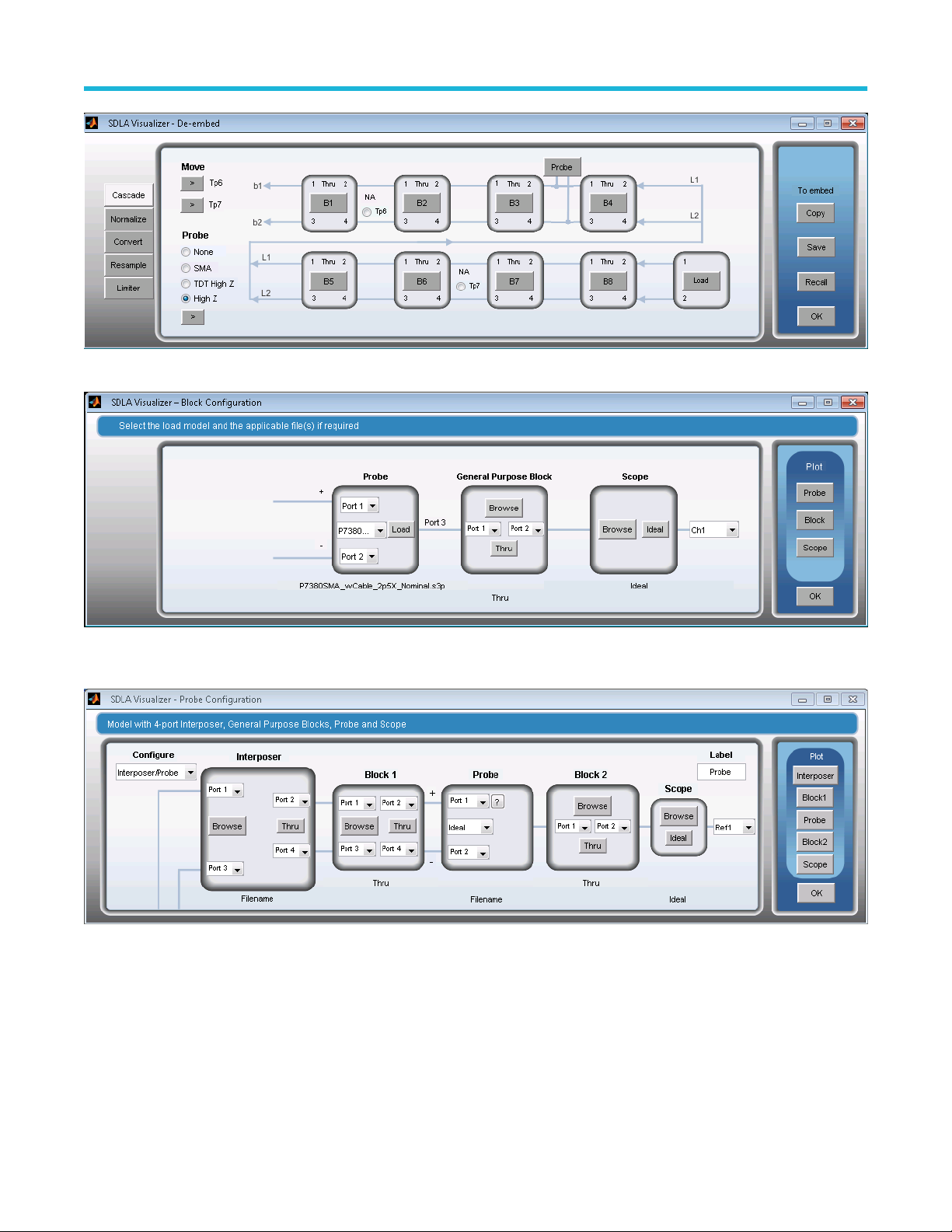
De-embed block
Pressing the Probe button on the Cascade T
Under Configure, select the circuit configuration desired. There is choice of Probe/Scope, shown above, or Interposer/Probe, shown
below:
ab diagram brings up the Probe Path Configuration Menu:
Or Interposer s6p, shown below:
SDLA Visualizer Serial Data Link Analysis Visualizer Software Application Help 52
Page 53
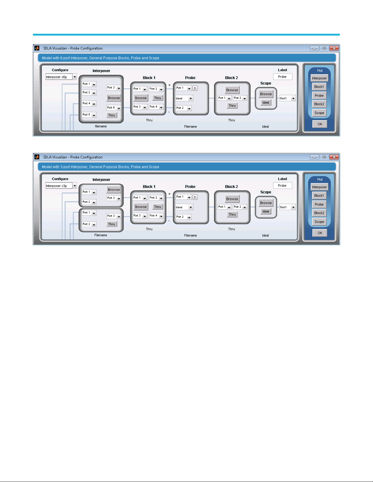
Or Interposer s3p, shown below:
De-embed block
Options
• Probe model: Use this drop-down menu to select the type of probe in use. This opens a file browser to the correct probe
directory
selecting the correct tip name for the file, see Probe and Tip Selection.. You may also press the ? button on the Probe panel.
• Probe Load: Press this to load a probe file according to the currently selected model.
• Port numbers: Select the desired port numbers to obtain the correct polarity connection for the probe.
• Scope Browse: Press this button to load an S-parameter file for the scope. This will open a browser and the user can select the
correct file according to the scope model in use.
• Scope Ideal: Press this button to use an ideal 50 Ohms termination to model scope.
• Interposer Browse: Press this to load 4-port S-parameters for the interposer model. This supports a simplified interposer model for a
differential clock or strobe line pair. Where the memory input and controller input are assumed to be one port per line, and the connect
to the probe are the other two ports.
• Interposer Thru: Press this to set the interposer to model two isolated ideal three way line connections.
• Interposer s6p Browse: Press this to load 6-port S-parameters for the s6p interposer model. This supports a complete two line
differential interposer model for a differential clock or strobe line pair. Where the memory input and controller input are modeled as
two ports per line, and the connection to the probe are the other two ports. The port number assignments for the s6p parameter is
as follows: the Tx side positive leg is connected to the top port on the left, the Tx side negative leg is connected to the second port
from the bottom on the left, the Rx side positive leg is connected to the second port from the top on the left, the Rx side negative
leg is connected to the bottom port on the left, the probe positive leg is connected to top port on the right, the probe negative leg is
connected to the bottom on the right.
• Interposer s6p Thru: Press this button to set the interposer to model two isolated ideal three way line connections.
. The user must then select the correct file according to the probe attenuation setting and according to the tip in use. For help
SDLA Visualizer Serial Data Link Analysis Visualizer Software Application Help 53
Page 54

De-embed block
• Interposer s3p Browse: Press this to load 3-port S-parameters for the s3p interposer model. This supports an interposer having the
same 3-port model on the positive leg and on the negative leg, and there is no coupling between the two lines. This configuration is
useful for single line signaling. The port number assignments for the s3p parameter are: the Tx side line is connected to the top port on
the left, the Rx side line is connected to the bottom port on the left, and the probe tip is connected to the port on the right
• Interposer s3p Thru: Press this button to set the interposer to model two isolated ideal three way line connections.
• Block 1 Browse: Press this button to load an S4p file for general purpose block 1. This general purpose block may be used to model
extra probe tip resistors.
• Block 1 Thru: Press this button to make general purpose block 1 be ideal Thru.
• Block 2 Browse: Press this button to load an S2p file for general purpose block 2. This general purpose block may be used to model
an RF switch.
• Block 2 Thru: Press this button to make general purpose block 2 be ideal Thru.
• Label: Edit this label to change the probe block label in the De-embed menu.
• Filenames: The filenames for the loaded S-parameter files are listed at the bottom of the menu.
• Interposer in Plot: Press this button to plot the interposer data. The interposer data could be s4p, s6p or s3p.
• Block1 in Plot: Press this button to plot the s4p data in Block1.
• Probe in Plot: Press this button to plot the s3p data of the Probe
• Block1 in Plot: Press this button to plot the s2p data in Block2.
• Scope in Plot: Press this button to plot the s1p data of the scope.
SEE ALSO:
• De-embed/Embed Menu
Probe and tip selection (RT only)
This topic explains how to identify probe tips and then select the proper file name for the configuration in use.
For the P7313 and 7380 probe models, the following set of tips is available; however
S-parameter sets. These are:
• HBW Right Angle Flex,
• HBW Straight Flex,
• Medium Flex Small Resistor,
• and Short Flex Small Resistor.
, only four of these tips are supported with
SDLA Visualizer Serial Data Link Analysis Visualizer Software Application Help 54
Page 55

De-embed block
Shown below are the tips for P75xx family of probes. However, only the Performance Solder Tip is currently supported with S-parameter
sets.
Choosing the correct 3-port S-parameter file
Press De-embed on the Main Menu. On the Cascade T
the diagram. This brings up the Probe Configuration menu:
SDLA Visualizer Serial Data Link Analysis Visualizer Software Application Help 55
ab, under Probe, select the High Z radio button. Then press the Probe button on
Page 56

De-embed block
On the Probe drop-down menu, choose the correct model that is in use. For example, P7380 was selected in the image above. The
browser will then open the correct directory for the selected probe model:
Choose the correct file for the probe’s current settings. Note that the file name contains the probe model, and a gain number such as 5X or
25X, and it also contains a name for the tip that is in use. Y
shown above.
The gain setting for a probe is indicated by LEDs on the probe comp box that plugs into the oscilloscope input channel connectors.
Note: T
ri-mode probes, such as the 75xx models, are able to operate under 4 possible modes. However, for SDLA, the
S-parameter support currently only allows a choice for differential mode, which is identified as A-B selection on the probe comp
box that plugs into the oscilloscope.
ou’ll need to correlate the tip name in the filename using the probe tip images
SMA Probes
The SMA probe S-parameter files include the matched pair of SMA cables that come with the probe. There are no tip selections. The
attenuator choice is included in the file name and the LEDs on the probe comp box indicate which setting is in use.
Scope Settings when Using a Probe with SDLA
The oscilloscope DSP filters must be turned on while using the probe in conjunction with SDLA. T
oscilloscope’s Vertical menu. Make sure that Digital Filters (DSP) Enabled radio button is selected. In addition, go to the scope’s Vertical
menu Chan X tab on the left, and select the channel which the probe is connected to. Then, on the scope menu, select Vertical > Probe
SDLA Visualizer Serial Data Link Analysis Visualizer Software Application Help 56
o check that they are turned on, go to the
Page 57

De-embed block
Cal. Press the Select button to bring up the probe tip selection menu. Make the radio button selection in this menu match the tip that is in
use on the probe. This insures that probe DSP is turned on. (Note: not all tips are supported with S-parameters, as mentioned above.)
Then, SDLA will correctly de-embed the current probe DSP response, and replace it with the probe combined with user data, and produce
the results in a math waveform slot on the scope display
does not include user data for the probe connection, but the test point math waveform created by SDLA will represent the response of the
system that includes both the probe and its actual connection to the DUT.
. This way, channel X of the scope will have the nominal filter response that
P7520A, P7625, P7630, P7633, and P77XX probes
For these probes, the S-parameters are stored internally in the probe. Therefore, they are loaded into SDLA directly from the scope. No file
browser is opened. A probe must be plugged into the oscilloscope source channel in order for the S-parameter set to be loaded into SDLA.
User DATA probes
In some cases, such as for interposer setups where custom modified probe tips are sometimes used, it may be that the oscilloscope does
not have nominal DSP probe data. In this case, on the scope menu, select Vertical > Probe Cal. Press the Select button to bring up the
probe tip selection menu. Choose Other Tip (no DSP). This way, the scope will not apply DSP for the given probe model. Instead, you
may use the user probe data that is selected from the probe drop-down menu under User. A file browser will open, and you may load the
custom probe data S-parameter set for use with the interposer. This data may be provided on a custom basis from Tektronix or from other
sources, such as a custom simulation model.
ou must have saved S-parameter data there prior to loading.
Note: Y
SEE ALSO:
• Configuring Probes
• De-embed/Embed Menu
Block configuration menu
Use the Block Configuration menu to configure the cascaded S-parameter modeling blocks B1–B8 in the De-embed/Embed Menu. (T
configure the final block, use the Load Configuration Menu.)
The Block Configuration menu has four tabs that offer different categories of models:
Thru Tab
The Thru block model is used when the block is not a necessary part of the cascade. It represents an ideal model that has no effect upon
signals in the system.
o
SDLA Visualizer Serial Data Link Analysis Visualizer Software Application Help 57
Page 58

File Tab
The File Tab allows you to choose from six models represented by data read from files:
16-Port
De-embed block
Extract a 4- port file from a single 16-port S-parameter file. Y
ports from the 16 ports. When apply is clicked, it plots the selected four port S-parameter. All S-parameter terms in the data are taken into
account when computing test point transfer functions.
ou can load a 16-port S-parameter file to represent the block. Select any four
12-Port
Extract a 4- port file from a single 12-port S-parameter file. Y
ports from the 12 ports. When apply is clicked, it plots the selected four port S-parameter. All S-parameter terms in the data are taken into
account when computing test point transfer functions.
ou can load a 12-port S-parameter file to represent the block. Select any four
SDLA Visualizer Serial Data Link Analysis Visualizer Software Application Help 58
Page 59

8-Port
De-embed block
Extract a 4- port file from a single 8-port S-parameter file. Y
ports from the 8 ports. When apply is clicked, it plots the selected four port S-parameter. All S-parameter terms in the data are taken into
account when computing test point transfer functions.
ou can load an 8-port S-parameter file to represent the block. Select any four
6-Port
Extract a 4- port file from a single 6-port S-parameter file. Y
ports from the 6 ports. When apply is clicked, it plots the selected four port S-parameter. All S-parameter terms in the data are taken into
account when computing test point transfer functions.
ou can load a 6-port S-parameter file to represent the block. Select any four
4-Port Single-ended
Models a single 4-port S-parameter set, as shown above. Y
terms in the data are taken into account when computing test point transfer functions.
ou can load a 4-port S-parameter file to represent the block. All S-parameter
4-Port Differential
Models a mixed mode S-parameter set.
You can load a 4-port S-parameter file that has been saved with a mixed mode format for the data. The differential block allows the
filename and path for the mixed mode S-parameters to be specified using a Browse button. The block is shown with two differential ports,
but physically it still has 4 single-ended ports. SDLA will convert the mixed mode data into a single-ended data format for use within the
cascade of blocks.
SDLA supports two ways of organizing the S-parameter data in the matrix. Typical shows a typical arrangement of mixed mode
S-parameter data read from the file. Alternate provides a second arrangement.
Note: The mixed mode representation of S-parameter data is not supported by the T
organizations of the file data is supported, as shown below:
SDLA Visualizer Serial Data Link Analysis Visualizer Software Application Help 59
ouchstone 1.0 file format. Therefore, only two
Page 60
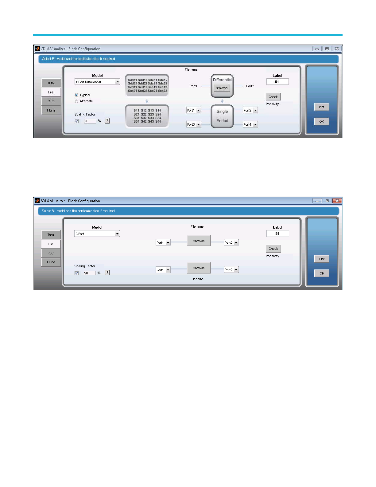
De-embed block
2-Port
Models two 2-port S-parameter sets.
This allows two 2-port S-parameter files to be loaded into the 4-port block model. SDLA will convert these into one 4-port S-parameter set
with ideal cross-coupling terms set to zero.
A common use for this choice would be to represent a pair of shielded cables connected between a fixture and the scope.
Transfer Function
Models a frequency domain set of complex data.
This allows two files containing transfer function data in the frequency domain to be loaded to represent the block. The file will be in the
ouchstone 1.0 format. This format contains a frequency column, a real or magnitude column and an imaginary or phase column.
s1p T
SDLA will convert these into a single 4-port S-parameter set with ideal cross-coupling and reflection coefficient terms set to zero. A
common use for this choice would be to represent a pair of shielded cables connected between a fixture and the scope.
SDLA Visualizer Serial Data Link Analysis Visualizer Software Application Help 60
Page 61

FIR
Models a time domain impulse response.
De-embed block
This allows two files containing FIR filter coef
oscilloscope arbflt() ASCII format. SDLA will convert these into one 4-port S-parameter set with ideal cross-coupling terms set to zero. The
reflection coefficient terms are also set to zero.
The file may contain comment lines with # as the first character. The file may contain multiple lines of filter coefficients, where the first
number followed by a “;” is the sample rate. The remaining numbers are the filter coefficients separated by space comma.
ficients data in the time domain to be loaded to represent the block. The file shall be in the
High Z probe
Models the loading of the probe.
This allows a 3-port S-parameter set representing a probe to be loaded. This model places the probe tips on line A and line B in parallel
with the signal path lines. A potential use would be to observe how oscilloscope or logic analyzer probes load the system.
Note: This model is representing probe loading ef
this model.
SDLA Visualizer Serial Data Link Analysis Visualizer Software Application Help 61
fects only. There is no acquired waveform entering the simulation system from
Page 62

De-embed block
TDT Waveforms
Models two waveforms from the TDT measurement. Press here for more information.
This allows two waveforms to be loaded as reference waveform and TDT waveform. These two waveforms are from the TDT
measurement. SDLA converts these into one 4-port S-parameter set. Insertion loss term is computed from these two waveforms.
A common use for this choice would be that TDT measurement is performed and the reference waveform and TDT waveform are obtained.
1-Port Shunt
Models two 1-port S-parameter sets in shunt connection. Press here for more information.
This allows two 1-port S-parameter files to be loaded as a shunt connection. SDLA converts these into one 4-port S-parameter set in
series.
A common use for this choice would be there are shunt connections represented by two 1-port S-Parameter files.
SDLA Visualizer Serial Data Link Analysis Visualizer Software Application Help 62
Page 63

De-embed block
2-Port Shunt
Models one 2-port S-parameter set in shunt connection. Press here for more information.
This allows one 2-port S-parameter file to be loaded as a shunt connection. SDLA converts these into one 4-port S-parameter set in series.
A common use for this choice would be that there are shunt connections represented by a 2-port S-Parameter file.
S Parameter Scaling
S Parameter Scaling is used to scale the S parameter
Scaling Factor is not changed with it.
When enabled, the scaled S parameter is plotted and applied to the cascading. Be aware, the crossing and reflection terms are zeroed out
during the scaling process, even at the 100% scaling. The default is 90%. Scaling is from 20% to 200%.
. The small square check box is used to enable or disable the Scaling Factor. The
RLC Tab
This allows RLC (resistor, inductor, and capacitor) elements to be used to model the block. SDLA computes a set of 4-port S-parameters
that will be used in the cascade. The cross-coupling terms will be set to zero.
SDLA Visualizer Serial Data Link Analysis Visualizer Software Application Help 63
Page 64

De-embed block
The RLC Tab Model drop-down menu of
fers six different series and shunt configurations of RLC networks.
Series 1
Represents a series RLC network in series with each line (shown above).
Series 2
Represents a parallel RLC network in series with each line:
Shunt 1
Represents series RLC networks in shunt with each line:
SDLA Visualizer Serial Data Link Analysis Visualizer Software Application Help 64
Page 65

Shunt 2
Represents parallel RLC networks in shunt with each line:
CRLC
De-embed block
Represents a shunt capacitor
RLCC
Represents a series resistor
, series inductor, series resistor and a shunt capacitor with each line:
, series inductor and two shunt capacitors with each line:
R, L, C, C2 edit boxes
These determine the values for these components.
SDLA Visualizer Serial Data Link Analysis Visualizer Software Application Help 65
Page 66

De-embed block
R, L, C, C2 check boxes
When checked, the R, L, C, or C2 value will be included in the circuit. When not checked, the R, L, C, or C2 element will be replaced with a
short if it is a series element, or with an open if it is a shunt element.
Freq Space MHz
This edit box specifies the frequency spacing for the S-parameter set that will be computed for this network. Frequency spacing determines
the time duration the S-parameter covers.
Label
This edit box determines what label will appear on the block diagram in the De-embed/Embed Menu, depending on which block this is
located in.
Plot
This will open a new window containing all the plot menus for the various ways in which the 4-port S-parameter set may be viewed.
OK
This menu button closes the block menu and returns to either the Embed or De-embed menu, depending on which one was used to open
the block.
T Line T
This allows you to define a lossless transmission line. SDLA computes a set of 4-port S-parameters depending on the parameter settings
in the edit boxes. The cross-coupling terms shall be set to zero. Press here for more information.
ab
Z0 ohms
This allows you to specify the characteristic impedance of the transmission line pair
.
Delay ns
This allows the delay through the transmission lines to be specified in ns.
Freq Space MHz
This specifies the frequency spacing for the 4-port S-parameter set that will be created for the transmission line model.
Plot
This may be used to view the characteristics.
SEE ALSO:
• De-embed/Embed Menu
SDLA Visualizer Serial Data Link Analysis Visualizer Software Application Help 66
Page 67

De-embed block
• Load Configuration Menu
Load configuration menu
The final block in the De-embed/Embed Menu cascade diagram is where you determine what will load the output ports of the cascaded
circuit. Pressing it brings up the Load Configuration menu. (T
De-embed Cascade Load Block
The final block on the De-embed Menu cascade diagram is labeled either Scope, SMAProbe (RT only) or Load. When you press it, a
different Load Configuration Menu will come up depending on how you have configured your model. For example, the image below shows
the default menu that comes up without a probe:
o configure blocks B1-B8, use the Block Configuration Menu.)
S-parameters for an ATI channel
• SX type scope If the source channel is A
1-Port from Model pull down list, two options show up for file loading;
1. Browse option lets you select any *.s1p file to load to the block.
2. Load ATI option automatically loads the ATI channel s-parameters to the block.
If, instead, you have configured it for an SMA Probe (RT only), the following menu comes up. The middle block allows for the effects of
cabling between the probe and the scope. For further information, see Configuring Probes.
TI, clicking the Load button in the De-embed menu will open the Load menu. After select
SDLA Visualizer Serial Data Link Analysis Visualizer Software Application Help 67
Page 68

De-embed block
If you have configured it for TDT High Z the following menu comes up. Blocks B1 through B7 are ignored and B8 is defined by time domain
waveforms.
Clicking the B8 button displays the following menu in which the B8 block can be defined by a reference and a TDT waveform.
Embed Cascade Load Block
The final block on the Embed Menu cascade diagram is labeled Rx Load. Pressing on it brings up the Load Configuration Menu show
below
, which allows you to determine the model that will load the output ports of the simulation circuit. In many cases, this would model a
physical receiver.
The impedance can be modeled as a nominal value, one 2-port S-parameter block, or two 1-port S-parameter blocks by choosing one of
the options in the Model drop-down list. By default, SDLA assumes 50 Ohm impedance. Below is the menu that comes up with one 2-port
S-parameter block:
SDLA Visualizer Serial Data Link Analysis Visualizer Software Application Help 68
Page 69

SEE ALSO:
• De-embed/Embed Menus
• Block Configuration Menu
De-embed block
SDLA Visualizer Serial Data Link Analysis Visualizer Software Application Help 69
Page 70

Plots
Plots
Plots
Plots are essential aids for setting up and verifying the system. SDLA V
the results of running the enabled processing blocks and the test points. These can be used along with DPOJET and oscilloscope plots
for tasks such as analyzing the quality of the S-parameters, verifying the configuration of each block as you configure the circuits, or
determining port numbers.
Navigation features include zoom (+) and pan tools; some plots also include measurement cursor tools.
isualizer provides a variety of context-sensitive plots that show
For some examples of how to troubleshoot using S-parameter plots, see Using Plots for T
Here are just some of the SDLA Visualizer plots available:
• Comprehensive S-parameter plots. Extensive plots of the S-parameters allows for full insight into the system characteristics. An
Overlay feature is available for some plots. Some examples of S-parameter plots:
• 6-port, 4-port, 3-port, 2-port, 1-port plots
Use these plots to:
• Quickly verify port assignment. You can tell by the shape of the curve which one is insertion loss.
• Validate that the magnitude is correct. Typically, the insertion loss should be higher at high frequencies; reflection and cross
talk is typically higher at higher frequencies.
• Do a passivity check. None of the S-parameters of a passive system should go above 0 dB in the frequency domain. All data
can be less than 0d and yet the system may still violate passivity where the total output power is more than the input power.
Note that viewing the plots is a first step only; for a more extensive check, go to a file load tab in a block menu. For cases
where the S-parameter data is loaded from a file, a passivity check button becomes available.
• Check whether models are Single-ended or Mixed Mode. For a single-ended system, transmission terms such as s21, s12,
s34, and s43 are equal for an ideal passive system. However, if the data had been converted to mixed mode, the common
SDLA Visualizer Serial Data Link Analysis Visualizer Software Application Help 70
roubleshooting S-parameters.
Page 71

mode transmission response is generally noticeably different than the differential transmission. In other words, S34 and S43
would equal common mode, and would look dif
ferent than the differential mode response plotted in S21 and S12.
Plots
• Impedance vs. magnitude (Plot Z(f) button)
These plots let you quickly observe how impedance varies over frequency for the reflection coefficients in the S-parameter set.
• Smith Chart impedance (Plot Z button)
A Smith Chart provides impedance, phase, and magnitude information, including impedance in polar or rectangular format,
markers readout, start and stop frequencies, and overlay:
SDLA Visualizer Serial Data Link Analysis Visualizer Software Application Help 71
Page 72

• Time Domain plots (Plot TD button), including impulse response vs. time and step response vs. time
Plots
In the time domain, all the plots should be settled by the end of the time record. If not, this could mean that the measurement was
performed with too short of a time interval. Note that if a pulse is close to the beginning of the record, such as a typical t1
should be expected that a portion of the non-causal response at the front is wrapped to the very end of the record. SDLA handles
the wrapped-end part internally.
This non-causal part is not real for the analog circuit that was measured; it is an artifact of the band-limiting effect of performing the
IFFT operation to transform the S-parameter set to the time domain.
If the frequency spacing is too wide, the time domain will show aliasing where the pulse is wrapped in the time domain to an
aliased position.
1, then it
SDLA Visualizer Serial Data Link Analysis Visualizer Software Application Help 72
Page 73

• Pressing Overlay on the left side lets you select up to 16 plots in one visual display. The overlay plot is performed on four axes:
Magnitude vs. Frequency
, Phase vs. Frequency, Impulse vs. Time and Step Response vs. Time:
Plots
The Overlay Menu is on the left side, with a Plot
vs. GHz, Phase in Degrees vs. GHz, Amplitude vs. Time, and Step Response vs. Time.
est point filter (transfer function) plots. Plots of test point filter responses allow for verification of the system setup. Any problems
• T
typically show up in the plots. Magnitude, Phase, Impulse and Step graphs are available.
button at the bottom. Pressing Plot opens a window with four overlaid axes: dB
SDLA Visualizer Serial Data Link Analysis Visualizer Software Application Help 73
Page 74

Plots
• Tx Emphasis plots. For details, see Tx Emphasis Menu.
Additional plots are available via:
• DPOJET eye diagram plots. When the Main Menu Config button is set for Auto Configure, then when the Apply button is pressed,
DPOJET will produce eye diagram plots for the test point waveforms that are turned on. These will include the source waveforms and
waveforms from one or more of the test points that are enabled. DPOJET can create a maximum of four plots. Therefore, it may be
necessary to go into the DPOJET menus to reassign the plots to view the waveforms desired. (T
Analyze>Jitter and Eye Analysis (DPOJET).)
• JNB eye diagram plots. JNB has an extensive collection of eye diagram plots as well as many jitter, noise, BER and spread spectrum
plots, displaying up to four plots at once. it may be necessary to go into the JNB plots to reassign the plots to view the waveforms
desired. (To do this, from the scope menu, press Applications > 80SJNB.)
• Scope waveform plots. The waveforms that represent the test points appear on the oscilloscope screen. They may be controlled for
viewing by using the standard oscilloscope controls. Cursor measurements and standard measurements may also be applied.
SEE ALSO:
• Using Plots for Troubleshooting S-parameters
• Understanding Test Points
o do this, from the scope menu, press
Using plots for troubleshooting s-parameters
SDLA Visualizer S-parameter plots include an Overlay tool, located on the left side, that allows you to view any selected plots on one
display. This can be helpful in many scenarios, such as:
• Viewing a DUT with Mismatched Differential Pairs
In this example, impulse plots reveal that the delay between transmission line pairs are not matched in length. In the overlay plot
below, the two lines have similar magnitude responses. However, the difference in delay between the two lines shows up in the phase,
impulse, and step response plots.
SDLA Visualizer Serial Data Link Analysis Visualizer Software Application Help 74
Page 75

• Troubleshooting bad VNA measurements using overlay plots
Plots
In this example, there is an open connection on one leg of the fixture and cables when measuring the S-parameters on a VNA. (Also
note the bad S1
good fixture.
1 and S22.) The other leg of fixture looks okay. All four plots circled on the image below should be similar-looking for a
• Troubleshooting bad phase response
In this example, the wrong calibration kit on VNA was used, which resulted in a bad phase response. The phase did not start at zero
degrees at DC. This, in turn, resulted in bad step response.
SDLA Visualizer Serial Data Link Analysis Visualizer Software Application Help 75
Page 76

• Verifying mixed mode vs. single-ended mode
Plots
Y
ou can use these plots to verify the difference between mixed mode and single-ended.
• Troubleshooting bad step response
In this case, the step response has a non-casual dip before the rising edge. The cause of this is revealed by observing the magnitude
response zoomed in at DC. The S-parameters commonly do not contain DC, because VNAs cannot measure it. SDLA must then
extrapolate the data to DC before it can be transformed to the time domain for processing to make a transfer function filter
Extrapolation can be problematic, as can be seen below, where the first data sample in the S-parameter set was lower than the
previous one due to noise or a bad VNA measurement. This results in the extrapolated portion of the curve being slightly offset by a
few tenths of a dB. This is enough to cause the pre-shoot dip in the step response, as shown below.
.
SDLA Visualizer Serial Data Link Analysis Visualizer Software Application Help 76
Page 77

SEE ALSO:
• Plots
• Examples of T
Plots
asks and Troubleshooting
SDLA Visualizer Serial Data Link Analysis Visualizer Software Application Help 77
Page 78

Tx block (Transmitter modeling block)
Tx block (Transmitter modeling block)
Tx block overview
ransmitter Modeling Block is the only block that contains a double definition: it is defined once for the Measurement Circuit model and
The T
again for the Simulation Circuit model.
A simple model assumes a perfect 50 Ohm environment. But what if the transmitter environment is not 50 Ohm? Using the Tx Block, you
can model different configurations, such as setting a nominal impedance. You can represent the transmitter as one 2 port S-parameter
model, or as two 1-port models. You can also use it to configure Emphasis options.
The source impedance is specified by the user, while the Thevenin equivalent voltage is computed by the software, based on the input
waveforms and system models defined by the user.
Thevenin Equivalent voltage: The Tx Block contains the Thevinin equivalent voltage, which has special importance to the system. It
is the point that contains the common waveform voltage that is shared by BOTH the Measurement Circuit (de-embed) path and the
Simulation Circuit (embed) path. In other words, this is the point where the acquired waveform is passed into the simulation side of the
system. Since a voltage source has zero impedance, this point provides isolation that prevents the Simulation Circuit from loading the
Measurement Circuit configuration.
Pressing on the Tx block brings up the Tx Configuration Menu. From there, you can select the Emphasis radio button and press on the
Emphasis button that appears on the diagram. This brings up the Tx Emphasis Menu.
SEE ALSO:
• Tx Configuration Menu
• Tx Emphasis Menu.
Tx configuration menu
Use this menu to model different transmitter configurations. You can reach it by pressing Tx on the Main Menu.
The transmitter representation is split into two Thevenin equivalent circuit models with a common differential voltage source. The top
section is the side for the Measurement Circuit (de-embed) path and the bottom is for the Simulation Circuit (embed) path. For example,
the graphic below shows a transmitter model using nominal impedance:
The following image represents the transmitter as one 2-port S-parameter model in the lower (embed) part of the systems, and two 1-port
S-parameter blocks in the upper (de-embed) part of the system. These are shown dif
both the upper and lower sections to be set up as identical to each other.
SDLA Visualizer Serial Data Link Analysis Visualizer Software Application Help 78
ferently to illustrate the choices; normal usage is for
Page 79

Tx block (Transmitter modeling block)
Select the Emphasis radio button. Press the Emphasis button that appears in the diagram, which brings up the Tx Emphasis Menu :
SEE ALSO:
• Tx Block Overview
• Tx Emphasis Menu.
Tx emphasis menu
The Tx Emphasis Menu lets you specify
a FIR filter file. You reach this menu by pressing Tx on the Main Menu, selecting the Emphasis radio button, and then pressing the
Emphasis button that appears on the diagram. Note that the Emphasis feature only appears in Simulation Circuit path.
, remove or add emphasis, de-emphasis or pre-emphasis filters. You may also read data from
SDLA Visualizer Serial Data Link Analysis Visualizer Software Application Help 79
Page 80

Tx block (Transmitter modeling block)
Four types of filter response are available. Each option offers the ability to either remove the effects of a component or to simulate one.
The Pre/De-emphasis units are in dB. Y
the source signal, press Apply on the Main Menu to recompute the system’s test point filters.
• Thru removes the effect of de-emphasis added by another circuit block or device.
• De- adds de-emphasis: it attenuates the low frequency components to compensate for high-frequency loss through the Channel.
Shown in the image above.
• Pre- adds pre-emphasis: it amplifies the high frequency components to compensate for high-frequency loss through the Channel.
• 3-tap FFE: High speed serial data standards require 3-tap FFE at the transmitter to compensate for the channel loss. When 3-tap FFE
is selected, SDLA shows three numerical controls for the three taps c-1, c0, and c1. You can enter in values for the three taps in linear
scale. When you Apply, SDLA computes the filter for the 3-tap FFE Tx equalizer. Make sure the DC term c0 is bigger than both c-1 and
c+1. Otherwise the equalizer will not be stabilizing.
ou can use the typical 3 dB setting or enter a custom dB setting. To see the results of the filter on
• Read from FIR File: The Emphasis block may be set up from a FIR filter file as follows:
Select the Read from FIR file radio button. Browse to the location of your filter file. The Emphasis FIR filter is combined into the test
point transfer function using the current sample rate setting of the oscilloscope. The file format contains comment lines starting with #.
It then contains at least one line formatted as: <sample rate>; coef1, coef2, ... coefN.
Note: The filter setup need not be an emphasis type. It may be of any type required to better simulate your system.
Specification Settings
Use the Specification settings that appear when you select the De- or Pre- radio button to add or remove emphasis values. The bit rate is
the bit rate of the source signal. It determines the frequency range increase or decrease in the magnitude response of the emphasis filter
The magnitude frequency response is periodic, with a period determined by the bit rate. The peak value of the filter magnitude response is
set by the dB value you chose.
.
SDLA Visualizer Serial Data Link Analysis Visualizer Software Application Help 80
Page 81

Plot button
Tx block (Transmitter modeling block)
Pressing Plot opens a window that contains four graphs: Magnitude vs. Frequency
and Step Response vs. Time. The image below shows a plot where de-emphasis with a setting of 3 dB was added:
, Phase vs. Frequency, Impulse Response vs. Time,
Plot with 3 dB of pre-emphasis added.
SDLA Visualizer Serial Data Link Analysis Visualizer Software Application Help 81
Page 82

Plot with 3 dB of de-emphasis removed.
Tx block (Transmitter modeling block)
Plot with 3 dB of pre-emphasis removed.
SEE ALSO:
SDLA Visualizer Serial Data Link Analysis Visualizer Software Application Help 82
Page 83

• Tx Block Overview
• Tx Configuration T
Tx block (Transmitter modeling block)
ool.
SDLA Visualizer Serial Data Link Analysis Visualizer Software Application Help 83
Page 84
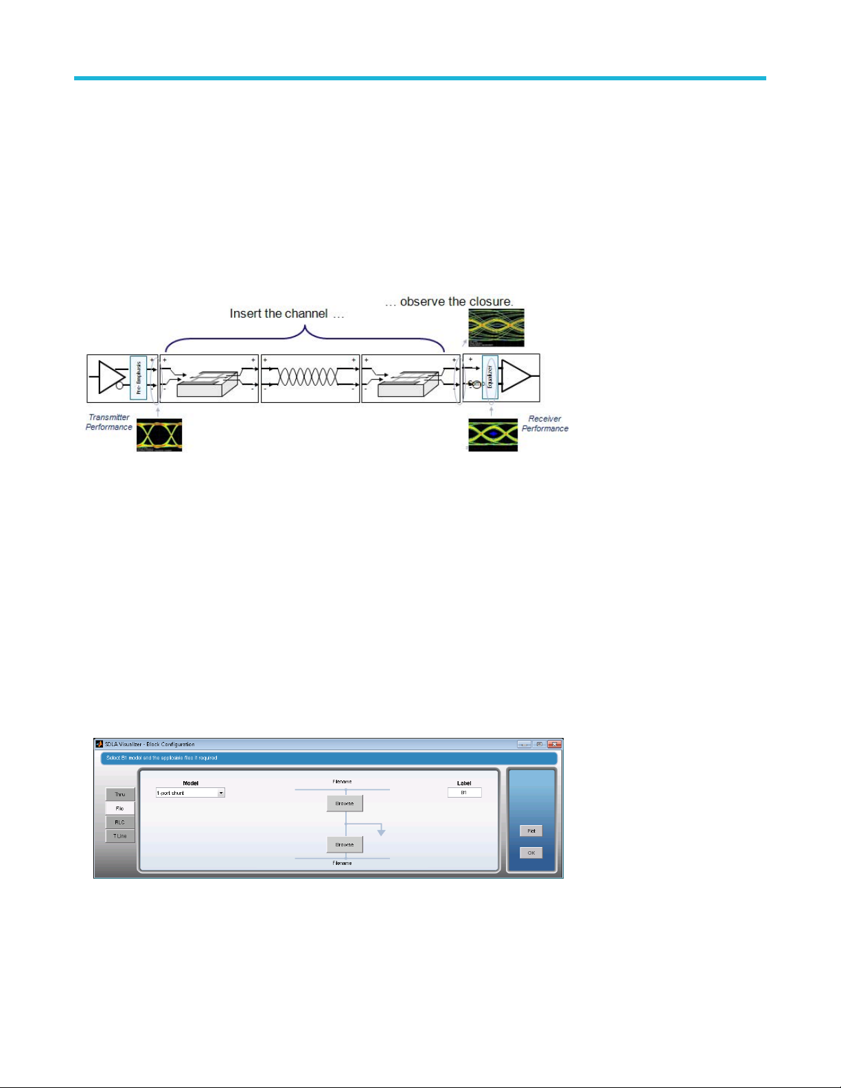
Embed block
Embed block
Embed block overview
The Embed Block represents a cascade of 4-port S-parameter models for simulating a desired system to be connected to the Tx model.
Models can be loaded from S-parameter files as 4-port, 3-port, 2-port, 1-port, or transfer functions. Models can be created from RLC
combinations, or a lossless transmission line. Probe load models are also included.
In a typical usage case, the testing of some serial standards requires the embedding of a compliance channel. But probing at the Rx pins is
often not possible, requiring simulation of the channel. The Embed Block lets you “insert” a simulated channel so that you can observe the
closed eye. Then, you can use the Rx Block to open the eye.
Create a simulated channel to embed by pressing Embed on the Main Menu. This brings up the Embed Menu. Using this, you may
configure the blocks in many ways. For more information, see De-embed/Embed Menu.
•
4-port single-ended S-parameter file
• 4–port differential S-parameter file
• Two 2-port S-parameter files
• FIR filter files (time domain)
• Transfer function files (frequency domain)
• High-Z probe
• TDT Waveform
• 6-port Single-ended
• 8-port Single-ended
• 12-port Single-ended
• 16-port Single-ended
SDLA Visualizer Serial Data Link Analysis Visualizer Software Application Help 84
Page 85

• Various RLC series or parallel configurations
• Lossless Transmission line model
• 3-port probe load model file
• 1-port load S-parameter file
• 2-port load S-parameter file
• Nominal load impedance
• TDT waveform block
SEE ALSO:
• De-embed/Embed Menu
Embed block
SDLA Visualizer Serial Data Link Analysis Visualizer Software Application Help 85
Page 86

Rx block (Receiver modeling block)
Rx block (Receiver modeling block)
Configure the Rx Block by pressing Rx on the Main Menu. This brings up the Rx Configuration Menu.
The Rx Block represents the model for the serial data link receiver for the Simulation Circuit. It restores the integrity of the data stream and
recovers the embedded clock. It can serve as a “reference receiver” in that it performs at the minimal acceptable level, as defined by a
standard, for a serial data receiver. (The analog part of a receiver, including the package and termination model, can be modeled using the
Embed Block, which contains the S-parameter files, transmission line, and RLC circuit models.)
The Rx Block equalizer compensates for the loss, cross-talk, reflection or noise in the link. It attempts to optimize the signal/noise ratio
of the eye opening, among other targets, in order to improve the link performance in aspects such as bit error rate. In the oscilloscope
measurement context, this equalization allows you to accurately simulate the signal timing and amplitude parameters at the receiver.
Sometimes, this measurement point may be referred to as a “virtual Rx”, reflecting the simulated nature of the signals.
The receiver has a comparator, or “slicer”, that determines whether a bit with value 0 or 1 is received in any unit interval. The exact timing
at the slicer is determined by the clock recovery in the receiver. But the virtual Rx is typically not directly accessible by probing or other
methods, so the Rx equalization must be simulated in order to get adequate measurements. Often the signal at the input of the equalizer
will have a “closed” eye. When correctly designed, the equalization will “open” the eye and increase the eye height, width, or both.
Use the Rx Block AFTER using the Embed Block to create and insert a channel, so you can observe the eye closure at the Rx load. The
Rx Block will then show what the signal will look like inside the Rx where the decision 0 or 1 is made by the comparator (aka the “slicer”)
after the Rx equalization.
Rx block overview (RT scopes)
The Rx Block contains:
• Mode choice of User, AMI or Thru
• CTLE equalizer (User mode)
• Clock recovery (User mode)
• FFE / DFE equalizer (User mode)
• PAM-4 versus NRZ configuration (User mode)
• Output of CTLE to oscilloscope Math channel (User mode)
• IBIS-AMI model of equalizer (AMI mode)
The Rx Block provides three equalizer modes: User, AMI, and Thru. In User mode, continuous-time linear equalizer (CTLE), feed-forward
equalizer (FFE), and decision feedback equalizer (DFE)) models are provided for you to try as serial data receivers typically contain them.
Also, user mode supports various equalization adaptation/optimization requirements, such as the LMS-based optimization criterion from
SAS 6G, and peak-to-peak based optimization criterion from PCI Express 3.0, as these standards call for "behavioral equalizers" that
can be modeled using CTLE and/or DFE. Note that SDLA not only provides implementation of such behavioral equalizers for various
standards, but it goes beyond them to simulate much more capable signal conditioning, and allows you to compare them.
AMI Mode is also available; this allows you to emulate IBIS-AMI models, which are descriptions of the equalizers provided by chip
designers and manufacturers, as well as EDA tools that provide similar plug-in functionality. This results in more precise simulated Rx
waveforms for measurements, comparison and validation.
SDLA Visualizer Serial Data Link Analysis Visualizer Software Application Help 86
Page 87

Rx block (Receiver modeling block)
Rx block overview (sampling scopes)
The Rx Block contains:
Mode choice of User or Thru
•
• CTLE equalizer (User mode)
The Rx Block provides two equalizer modes: User and Thru. In User mode, continuous-time linear equalizer (CTLE) models are provided
for you to try, as serial data receivers typically contain them. Also, user mode supports various equalization adaptation/optimization
requirements, such as the LMS-based optimization criterion from SAS 6G, and peak-to-peak based optimization criterion from PCI Express
3.0, as these standards call for "behavioral equalizers" that can be modeled using CTLE. Note that SDLA not only provides implementation
of such behavioral equalizers for various standards, but it goes beyond them to simulate much more capable signal conditioning, and
allows you to compare them.
Specifying FFE/DFE on a sampling scope is done with JNB. JNB's top level equalization menu looks as follows.
SEE ALSO:
• Rx Configuration Menu
Rx configuration menu
Press Rx on the Main Menu to bring up the Rx Configuration Menu. This of
and Thru.
SDLA Visualizer Serial Data Link Analysis Visualizer Software Application Help 87
fers you three modes in the radio buttons on the left: User, AMI,
Page 88

User Mode
Rx block (Receiver modeling block)
User Mode gives you access to equalization tools and options for recovering the data stream and clock by correcting for the ef
of insertion loss, cross talk, reflection, and noise. Many CTLE, clock recovery and FFE/DFE parameters can be specified, plus Taps
definition and training sequence detection. This mode also implements the behavioral equalizers of PCI Express, SAS, USB, etc.
fects
Config Tab
On the Config T
When both sets of equalizers are enabled, the CTLE equalization occurs first, followed by the FFE/DFE equalization.
The following sections provide usage details:
• Using CTLE to Improve Signal Recovery
• Using PCIE/USB3.1/MIPI/CAUI-4/TBT Option in CTLE
• Using Clock Recovery for FFE/DFE Equalization
• Using FFE/DFE to Improve Signal Recovery
• Using PCIE/USB3.1 GEN2/MIPI/CAUI-4/TBT Option in FFE/DFE
• Using the Taps Tab
• Manual FFE/DFE configuration for PCIE/USB/MIPI/CAUI-4/TBT options
• Equalizing PAM-4 signals
• Running the Rx Equalizer in User Mode
ab, the equalization processing runs from left to right. The CTLE and FFE/DFE equalizers may be enabled separately.
AMI Mode (RT only)
AMI Mode allows you to emulate IBIS-AMI models, which are descriptions of the equalizers provided by chip designers and manufacturers,
as well as EDA tools that provide similar plug-in functionality. Note that SDLA only emulates the digital part of the IBIS-AMI model in the Rx
block. The analog part of the model is neglected in the Rx block, but can be modeled using the Embed block, where the S parameter file,
T-line model, and RLC circuit models can be used to model the Rx package and terminations.
For more details, see Rx AMI Mode
SDLA Visualizer Serial Data Link Analysis Visualizer Software Application Help 88
Page 89

Rx block (Receiver modeling block)
Thru Mode
When using Thru mode, the output of EQ Tp4, is the same as the input to EQ Tp3. Note that selecting Thru on the Rx Configuration Menu
does not alter the panels displayed.
SEE ALSO:
• Rx Block Overview
• Rx AMI Mode
Using CTLE to improve signal recovery
o use the CTLE equalizer, press Rx on the Main Menu to open the Rx Configuration Menu. Select User. On the Config tab, the
T
Equalizer: CTLE panel is on the left. Toggle the CTLE ON or OFF using the radio buttons in the upper left.
The CTLE output waveform is Tp10. Pressing Tp10 in the CTLE panel brings up the Test Point and Bandwidth Manager, where Tp10 can
be assigned to a Math channel like other test points.
You may need to adjust the CTLE settings in order to recover the data and clock signals. You can plot the CTLE by pressing the Plot
button on the right. It shows both the frequency domain and time domain responses of CTLE.
Second-order CTLE
Many standards such as PCIE Gen3 and USB 3.0 define a second-order CTLE. The function of most of the key parameters of the
second-order CTLE described here are shown in the following illustration. Refer to it as you review the parameter descriptions in the list
that follows.
SDLA Visualizer Serial Data Link Analysis Visualizer Software Application Help 89
Page 90

Frequency
Most of the following parameters are defined in serial data standards.
Rx block (Receiver modeling block)
A
dc
This is the DC gain of the CTLE transfer function. It is a positive number in linear scale. The default value is 0.8.
F
z
This is the zero frequency of the CTLE transfer function. The value must be within the range of 1 MHz to 20 GHz. The default value is
750 MHz.
F
p1
This is the frequency of the first pole of the CTLE transfer function. The value must be within the range of 1 MHz to 20 GHz. The default
value is 3.75 GHz.
F
p2
This is the frequency of the second pole of the second order CTLE transfer function. The value must be within the range of 1 MHz to
20 GHz. The default value is 5 GHz.
Another convention on the second order CTLE is used in standards such as SuperSpeed Gen 2 reference CTLE uses the following
convention:
SDLA Visualizer Serial Data Link Analysis Visualizer Software Application Help 90
Page 91

Rx block (Receiver modeling block)
Note: Both formulas (CTLE -1 and CTLE - 2) have four independent variables to configure.
IIR
This option, found in the CTLE T
an ASCII text file with file extension .tsf. The file uses a polynomial transfer function or zero-pole (factored) transfer function to define the
IIR filter. There is no limit on the order of polynomials. The file uses # to indicate a comment line; Numerator as the key word for the
numerator polynomial, and Denominator as the key word for the denominator polynomial. For example, if an IIR is a first order filter having
the pole at 4 GHz, then the denominator should be written as 1, 2*pi*4*1e6.
The following is an example IIR filter file definition:
# IIR CTLE Filter
# defined by a polynomial transfer function
#
# b1s^(n-1)+b2s^(n-2)+...+bn
# H(s) = - - - - - - - - - - - - - - -
SDLA Visualizer Serial Data Link Analysis Visualizer Software Application Help 91
ype drop-down menu, loads a custom IIR filter file that sets the CTLE parameters. The IIR filter file is
Page 92

# a1s^(m-1)+a2s^(m-2)+...+am
#
#
# using the following format
#
#[Numerator]
#b1, b2, ..., bn
#[Denominator]
#a1, a2, ..., am
#
# Note that unit is radian/second, not Hz
[Numerator]
5.026548245743669e+010, 3.158273408348595e+020
[Denominator]
Rx block (Receiver modeling block)
1, 6.283185307179587e+010, 6.316546816697189e+020
Note: The frequency unit is radians/second, not Hz.
In zero-pole form, the file uses Zeros as the key word for the zero frequencies, Poles as the key word for the pole frequencies, Unit as the
key word for the unit of the zero/pole frequencies, and DC Gain as the key word for the DC gain (in linear scale). V
GHz, MHz, kHz, Hz.
The following is an example IIR filter file definition (zero-pole form):
# IIR CTLE Filter
#
# A transfer function expressed in zero-pole (factored) form is
#
# (s+fz1)(s+fz2)...(s+fzn)
# H(s) = K * --------------------------
# (s+fp1)(s+fp2)...(s+fpm)
#
# where, K = Adc*(fp1*fp2*...*fpm)/(fz1*fz2*...*fzn) and Adc is the DC gain
# in linear scale.
alid unit options are
#
# The file format is
# [Unit]
# GHz {MHz,kHz,Hz}
SDLA Visualizer Serial Data Link Analysis Visualizer Software Application Help 92
Page 93

Rx block (Receiver modeling block)
# [DC gain]
# Adc
# [Zeros]
# fz1
# fz2
# ...
# fzn
# [Poles]
# fp1
# fp2
# ...
# fpm
#------------------------------------------------------------------------------
[Unit]
GHz
[DC gain]
0.8
[Zeros]
0.75
[Poles]
3.75
SDLA generates FIR filters (based on the IIR filter definition and complete signal path ) on pressing the Apply
the Run Eq button in the Rx Configuration menu. If CTLE output Tp10 is assigned to a Math waveform and turned on, then SDLA writes
the Tp10 FIR filter file (sdlatp10.flt) to C:\TekApplications\SDLA\output filters and configures the Math setup to utilize that filter.
button in the Main Menu or
FIR
This button opens a file browser to load a custom FIR filter to set the CTLE parameters.
Serial Data Standards
A serial data standard can be selected from the CTLE type dropdown. The SDLA Visualizer will run an optimization process to find the best
CTLE setting to maximize eye area or eye height. The following standards are available in the drop-down menu:
• PCIe Gen3: 2-pole/1-zero design with 7 presets [1]
• PCIe Gen4: 2-pole/1-zero design with 7 presets [1]
• PCIe Gen5: 4-pole/2-zero design with 11 presets [1]
• USB 3.1 Gen1 Short: 2-pole/1-zero design per [2]
• USB 3.1 Gen1 Long: 2-pole/1-zero design per [2]
• USB 3.1 Gen2: 2-pole/1-zero design with 7 presets [2]
• MIPI MPHY HS G4 (obselete): 2-pole/1-zero design with 11 presets [3]
• MIPI MPHY HS G4: 2-pole/1-zero design with 4 presets [4]
• MIPI MPHY HS G5: 2-pole/1-zero design with 10 presets [5]
SDLA Visualizer Serial Data Link Analysis Visualizer Software Application Help 93
Page 94

Rx block (Receiver modeling block)
• CAUI-4: 2-pole/1-zero design with 9 presets [6]
DisplayPort 1.4: 2-pole/1-zero design with 10 presets [7]
•
• DisplayPort 2.0 UHBR10: 2-pole/1-zero design with 10 presets [8]
• DisplayPort 2.0 UHBR13.5: 2-pole/1-zero design with 10 presets [8]
• DisplayPort 2.0 UHBR20: 2-pole/1-zero design with 10 presets [7]
• Thunderbolt 10 Gb/s: 2-pole/1-zero design with 10 presets [9]
• Thunderbolt 10.3125 Gb/s: 2-pole/1-zero design with 10 presets [9]
• Thunderbolt 20 Gb/s: 2-pole/1-zero design with 10 presets [9]
• Thunderbolt 20.625 Gb/s: 2-pole/1-zero design with 10 presets [9]
• HDMI 2.1: 2-pole/1-zero design with 8 presets [10]
• DDR5: DFE gain with 7 presets [11]
Results File
Press Results in the far right panel to view the contents of the optimization results file. The best CTLE setting is labeled with ***, where the
best setting has the maximum eye area/height value. An example for PCIe Gen4 is shown below.
# PCIE4 equalizer adaptation results
# Time: 08-Oct-2021 16:19:15
Adc(dB) Adc(lin) DFEtap1(mV)DFEtap2(mV)EA(UI*mV) EH(mV) EW(UI) fz1(GHz) fp1(GHz) fp2(GHz)
-6 0.501 27.01 2.23 80.89 105.15 0.77 1.00 2.00 16.00
-7*** 0.447 25.15 0.39 87.72 109.69 0.80 0.89 2.00 16.00
-8 0.398 21.91 -1.72 86.37 109.88 0.79 0.80 2.00 16.00
-9 0.355 20.35 -4.02 79.32 104.57 0.76 0.71 2.00 16.00
-10 0.316 18.24 -5.32 70.27 97.38 0.72 0.63 2.00 16.00
-11 0.282 16.70 -7.01 61.73 91.14 0.68 0.56 2.00 16.00
-12 0.251 15.31 -8.70 54.20 85.48 0.63 0.50 2.00 16.00
Using clock recovery for FFE-DFE equalization
o use the clock recovery function, press Rx on the Main Menu to open the Rx Configuration Menu. Select User. On the Config tab, the
T
Clock Recovery panel is in the middle.
Clock recovery is used for FFE/DFE equalization in the Rx Block. The software performs clock recovery by emulating a phase locked loop
(PLL) circuit. Use the data rate defined for the serial standard you are testing. If you are testing a new serial line, you may need to measure
the bit rate near the transmitter
is opened for bit rate measurement. You can also use the Auto Detect option in the Clock Recovery panel to identify the bit rate.
Scroll down for information on Troubleshooting Clock Recovery.
SDLA Visualizer Serial Data Link Analysis Visualizer Software Application Help 94
, or after some equalization (i.e., Tx emphasis equalization, Rx equalizations such as CTLE) so that the eye
Page 95

Rx block (Receiver modeling block)
Nominal Bit Rate
The nominal bit rate of the signal. It is typically specified by a serial data standard if the signal is generated from a device designed based
on standards. If it may vary
Note: The nominal bit rate you enter must be accurate, or you’ll need to press the radio button to recover the data and clock
signals.
, then the Auto Detect option could be helpful.
Auto Detect
When this radio button is selected, SDLA searches in the neighborhood of the nominal bit rate to detect the correct bit rate of the signal.
After using the detect bit rate to open the eye, you can further tweak the nominal bit rate based on the detected bit rate to tune the clock
recovery settings.
Note: If SDLA detects spread spectrum clocking (SSC) in the input waveform, Auto Detect is turned on.
Clk Delay (ps)
The clock delay is a specific delay added to the recovered clock after the PLL result. The value adjusts the clock of
equalization result and achieve the best data recovery.
fset to optimize the
Custom PLL Type I and Type II
Bandwidth (BW). The -3 dB bandwidth of the high-pass observed jitter transfer function (OJTF). The value should be specified in the serial
standard. For Type I PLLs, the OJTF bandwidth and the loop bandwidth are the same.
Damp. This is the damping ratio of the Type II PLL. The value should be spcified in the serial standard.
Serial Data Standards
The following standards are available on the drop-down menu:
• PCIe Gen3: 5th-order loop per [1]
• PCIe Gen4: 5th-order loop per [1]
• PCIe Gen5: 5th-order loop per [1]
Explicit Clock
An explicit clock is used for memory applications.
Clock Input
This is the source of the clock waveform.
Autoset Clk Delay
When selected, the SDLA Visualizer automatically finds the optimal clock delay, within 1 UI, that maximizes eye height of the data signal.
The delay is recorded in the Clk Delay (ps) edit box.
Note: The Clock Input is required to be continuous, not bursty (normal memory operation). Therefore, a special setup is required
for the controller that is driving the memory.
Troubleshooting Clock Recovery
If clock recovery fails, your bit rate might not be what you expect. One solution is to select Auto Detect in the Clock Recovery panel, as
described above. Another solution is to measure the bit rate as near to the transmitter as possible. Y
running on the oscilloscope to accurately measure the bit rate.
ou can use the DPOJET application
Training Sequence Functions
Another technique is to use the Training Sequence functions to help the Rx Equalizer identify the correct bit sequence before again running
your test signal through the Rx Equalizer.
SDLA Visualizer Serial Data Link Analysis Visualizer Software Application Help 95
Page 96

Rx block (Receiver modeling block)
The image below shows the T
1. Use a signal source with the same data pattern as the signal you plan to test, but with a clean, open eye pattern. This signal could
be one acquired close to the transmitter
emphasis or Rx CTLE to improve the eye opening.
2. On the Rx Configuration menu, select the TrainSeq tab. Set the correct Pattern Length according to the standard; for example, 127
for a PRBS7 data pattern.
3. Press the Detect button. You should see a Bit Sequence displayed in the left field, which should be the same bit sequence as in your
original signal.
4. With the correct bit sequence in place, select the Config tab and select the original test source.
5. Select (enable) the Use TrainSeq box if not already enabled. Enter the correct bit rate if you changed it in a preceding step.
6. Press the Run Eq button.
7. Check the results on the oscilloscope display. You should see a recovered data signal, though it may not meet the standard
specifications. You may need to address other design issues to correct any problems with the recovered data.
rainSeq tab of the Rx Configuration menu:
, or a slower speed version of the original signal, or the original signal compensated using Tx
Checking Test Point Filters
Another area for investigation is whether your test point filters are correct. Review the plots for those filters to determine whether
high-frequency noise or other aberrations are corrupting the signal. Use the global bandwidth filters to reduce such noise.
SEE ALSO:
• Using CTLE
• Using FFE/DFE to Improve Signal Recovery
• Rx Configuration Menu
• Rx Block Overview
Using FFE-DFE to improve signal recovery
To use the FFE/DFE equalizers, press Rx on the Main Menu to open the Rx Configuration Menu. Select User. On the Config tab, the
Equalizer: FFE/DFE panel is on the right.
You may adjust the Rx Equalizer settings in order to recover the data and clock signals by using many of the same techniques used to
optimize a hardware receiver.
SDLA Visualizer Serial Data Link Analysis Visualizer Software Application Help 96
Page 97

Adapt Taps
The following selections are available in the drop-down menu:
Rx block (Receiver modeling block)
• Auto: The adaptation routine starts by identifying initial T
• From Current: The adaptation routine uses current Taps values as the initial Taps settings, then adjusts them to optimize recovery of
the data and clock. The initial Taps settings might be those saved from an earlier test.
• None: The Rx equalizer uses the current Taps either from your inputs or from a previous adaptive session. Use the entered values
without changes. This option is useful when you want to load a known Taps file in the Taps tab to resume a test started earlier.
Most of the following parameters are defined in a serial data standard:
ap settings and then adjusts them to optimize recovery of the data and clock.
FFE Taps
The Feed-Forward Equalizer tap number is normally set to a number defined by the serial data standard. A value of FFE Taps = 0 means
the FFE has one Tap with Tap coefficients fixed to 1, signifying that FFE is off. The default value is 0.
Sample/bit
Sample per bit specifies the number of FFE Taps per bit. If set to >1, it implies an FFE with fractional spaces. The default value is 1.
Ref Tap
The Reference Tap for the FFE indicates the number of precursor Taps. It must be set to one (1) more than a multiple of the number of
FFE Taps per bit. The default value is 1.
DFE Taps
The DFE Taps number is normally set to a number defined by the serial data standard. For example, the setting for SAS is 3, and the
setting for PCIE Gen3 is 1.
Amplitude
The Amplitude is the target output amplitude for the Rx Equalizer. When you select Autoset Voltages (Autoset V checkbox), the adaptation
routine adjusts this value automatically to optimize the recovery of the data signal. The default value is 0.15 V.
Threshold
The Threshold is the middle voltage level of the signal, which may be the transition between logic levels. For biased signals, enter the
mid-level value. For differential signals, the value should be close to 0 V. The default value is 0 V. Lacking clear knowledge of the correct
voltage, use the Autoset Voltages function to determine the optimal value.
Use TrainSeq
Enables the Rx Equalizer to optimize its adaptation routine over a specific pattern the length of which is defined on the TrainSeq tab.
SDLA Visualizer Serial Data Link Analysis Visualizer Software Application Help 97
Page 98

Autoset V
Rx block (Receiver modeling block)
When Autoset V
the data and clock.
oltages is enabled, the Rx Equalizer adaptation routine adjusts the Amplitude and Threshold values to optimize recovery of
Serial Data Standards
The following standards are available in the drop-down menu:
• PCIe Gen3: 1-tap DFE per [1]
• PCIe Gen4: 2-tap DFE per [1]
• PCIe Gen5: 3-tap DFE per [1]
• USB 3.1 Gen2: 1-tap DFE per [2]
• MIPI MPHY HS G4: 1-tap DFE per [3]
• MIPI MPHY HS G5: 1-tap DFE per [3]
• CAUI-4: 5-tap DFE per [6]
• DisplayPort 1.4: 1-tap DFE per [7]
• DisplayPort 2.0 UHBR10: 1-tap DFE per [7]
• DisplayPort 2.0 UHBR13.5: 1-tap DFE per [7]
• DisplayPort 2.0 UHBR20: 1-tap DFE per [7]
• Thunderbolt 10 Gb/s: 1-tap DFE per [9]
• Thunderbolt 10.3125 Gb/s: 1-tap DFE per [9]
• Thunderbolt 20 Gb/s: 1-tap DFE per [9]
• Thunderbolt 20.625 Gb/s: 1-tap DFE per [9]
• HDMI 2.1: 1-tap DFE per [10]
• DDR5: 4-tap DFE per [11]
Using the taps tab
The settings on the Taps Tab (on the Rx Configuration Menu with User mode selected) reflect the settings on the Config Tab. For
example, in the following figure, the FFE Taps have a value of 1, and the DFE field shows 3 Taps with different values. This state results
from settings on the Config tab, where FFE is set to 0 and DFE set to 3. If this was the result of setting Adapt Taps to Auto, you could save
the results in a Tap file for use in a later Rx Equalizer run.
When PCIE3/USB3.1 Gen2/MIPI is selected in the FFE/DFE panel (in the drop-down menu under FFE/DFE T
Current is selected under Adapt Taps, the DFE adaptation algorithms attempt to maximize the eye area. The resulting DFE tap value is
shown in the Taps tab.
ype), and Auto or From
SDLA Visualizer Serial Data Link Analysis Visualizer Software Application Help 98
Page 99

Rx block (Receiver modeling block)
The Config Tab Results button is enabled on the right panel (under Output) when PCIE/USB3.1 Gen2/MIPI is selected, and Auto
or From Current is selected under Adapt T
pcieAdaptationEQ.txt. This results file has better numerical resolution for DFE Tap(mv) than what is shown in the Taps tab. Note that the
DFE tap value is between -30 mV and 30 mV per PCIE Gen3 specifications.
aps. After adaptation is finished, press Results to open the adaptation results file
For a complete description of AMI files, visit the IBIS Open Forum at http://www.eda.org/ibis. See especially the I/O Buffer Information
Specification for IBIS 5.1, AMI Executable Model File Programming Guide (section 10) and AMI Parameter Definition File Structure
(Section 10A) at http://eda.org/pub/ibis/ver5.1/ver5_1.pdf.
SEE ALSO:
• Using FFE/DFE to Improve Signal Recovery
• Rx Configuration Menu
• Rx Block Overview
Manual FFE/DFE configuration for Serial Data Standards
Setting CTLE T
and clock recovery parameters.
SDLA now provides the option to enable editing these parameters for advanced users. Choose Manual from the drop-down box next to
CTLE Type. This box does not appear for Standard/IIR/FIR and is set to Auto by default.
ype to any of the Serial Data Standards options grays out the Rx panel and disables changes to many of the equalization
SDLA Visualizer Serial Data Link Analysis Visualizer Software Application Help 99
Page 100

Rx block (Receiver modeling block)
As seen in the image, Manual modes enables editing of the field values on the Equalizer: FFE/DFE panel. Equalizer: CTLE and Clock
Recovery panels remain unchanged.
Equalizing P
When the incoming signal is PAM-4, select PAM-4 in the top right corner of Equalizer: FFE/DFE panel, as in the below image.
Currently PAM-4 does not apply to any of the supported standards. Therefore, once the PAM-4 option is selected, CTLE Type can only be
set to Standard/IIR/FIR, while FFE/DFE Type can only be set to Custom.
Similarly, PAM-4 DFE utilizes the LMS-based optimization criterion from SAS 6G.
AM-4 signals
Running the Rx equalizer
The following steps describe how to make a first run of the Rx Equalizer to determine whether further adjustments are necessary.
SDLA Visualizer Serial Data Link Analysis Visualizer Software Application Help 100
 Loading...