

Page 1

PIO-SSR Series
User’s Guide
A GREATER MEASURE OF CONFIDENCE
Page 2

WARRANTY
Hardware
Keithley Instruments, Inc. warrants that, for a period of one (1) year from the date of shipment (3 years for Models 2000,
2001, 2002, 2010 and 2700), the Keithley Hardware product will be free from defects in materials or workmanship. This
warranty will be honored provided the defect has not been caused by use of the Keithley Hardware not in accordance with
the instructions for the product. This warranty shall be null and void upon: (1) any modification of Keithley Hardware that
is made by other than Keithley and not approved in writing by Keithley or (2) operation of the Keithley Hardware outside
of the environmental specifications therefore.
Upon receiving notification of a defect in the Keithley Hardware during the warranty period, Keithley will, at its option,
either repair or replace such Keithley Hardware. During the first ninety days of the warranty period, Keithley will, at its
option, supply the necessary on site labor to return the product to the condition prior to the notification of a defect. Failure
to notify Keithley of a defect during the warranty shall relieve Keithley of its obligations and liabilities under this
warranty.
Other Hardware
The portion of the product that is not manufactured by Keithley (Other Hardware) shall not be covered by this warranty,
and Keithley shall have no duty of obligation to enforce any manufacturers' warranties on behalf of the customer. On those
other manufacturers’ products that Keithley purchases for resale, Keithley shall have no duty of obligation to enforce any
manufacturers’ warranties on behalf of the customer.
Software
Keithley warrants that for a period of one (1) year from date of shipment, the Keithley produced portion of the software or
firmware (Keithley Software) will conform in all material respects with the published specifications provided such Keithley
Software is used on the product for which it is intended and otherwise in accordance with the instructions therefore.
Keithley does not warrant that operation of the Keithley Software will be uninterrupted or error-free and/or that the Keithley
Software will be adequate for the customer's intended application and/or use. This warranty shall be null and void upon any
modification of the Keithley Software that is made by other than Keithley and not approved in writing by Keithley.
If Keithley receives notification of a Keithley Software nonconformity that is covered by this warranty during the warranty
period, Keithley will review the conditions described in such notice. Such notice must state the published specification(s)
to which the Keithley Software fails to conform and the manner in which the Keithley Software fails to conform to such
published specification(s) with sufficient specificity to permit Keithley to correct such nonconformity. If Keithley determines that the Keithley Software does not conform with the published specifications, Keithley will, at its option, provide
either the programming services necessary to correct such nonconformity or develop a program change to bypass such
nonconformity in the Keithley Software. Failure to notify Keithley of a nonconformity during the warranty shall relieve
Keithley of its obligations and liabilities under this warranty.
Other Software
OEM software that is not produced by Keithley (Other Software) shall not be covered by this warranty, and Keithley shall
have no duty or obligation to enforce any OEM's warranties on behalf of the customer.
Other Items
Keithley warrants the following items for 90 days from the date of shipment: probes, cables, rechargeable batteries, diskettes,
and documentation.
Items not Covered under Warranty
This warranty does not apply to fuses, non-rechargeable batteries, damage from battery leakage, or problems arising from
normal wear or failure to follow instructions.
Limitation of Warranty
This warranty does not apply to defects resulting from product modification made by Purchaser without Keithley's express
written consent, or by misuse of any product or part.
Page 3

Disclaimer of Warranties
EXCEPT FOR THE EXPRESS WARRANTIES ABOVE KEITHLEY DISCLAIMS ALL OTHER WARRANTIES,
EXPRESS OR IMPLIED, INCLUDING WITHOUT LIMITATION, ALL IMPLIED WARRANTIES OF MERCHANTABILITY AND FITNESS FOR A PARTICULAR PURPOSE. KEITHLEY DISCLAIMS ALL WARRANTIES WITH
RESPECT TO THE OTHER HARDWARE AND OTHER SOFTWARE.
Limitation of Liability
KEITHLEY INSTRUMENTS SHALL IN NO EVENT, REGARDLESS OF CAUSE, ASSUME RESPONSIBILITY FOR
OR BE LIABLE FOR: (1) ECONOMICAL, INCIDENTAL, CONSEQUENTIAL, INDIRECT, SPECIAL, PUNITIVE OR
EXEMPLARY DAMAGES, WHETHER CLAIMED UNDER CONTRACT, TORT OR ANY OTHER LEGAL THEORY,
(2) LOSS OF OR DAMAGE TO THE CUSTOMER'S DATA OR PROGRAMMING, OR (3) PENALTIES OR PENALTY
CLAUSES OF ANY DESCRIPTION OR INDEMNIFICATION OF THE CUSTOMER OR OTHERS FOR COSTS, DAMAGES, OR EXPENSES RELATED TO THE GOODS OR SERVICES PROVIDED UNDER THIS WARRANTY.
Keithley Instruments, Inc.
Sales Offices: BELGIUM: Bergensesteenweg 709 • B-1600 Sint-Pieters-Leeuw • 02-363 00 40 • Fax: 02/363 00 64
CHINA: Yuan Chen Xin Building, Room 705 • 12 Yumin Road, Dewai, Madian • Beijing 100029 • 8610-6202-2886 • Fax: 8610-6202-2892
FINLAND: Tietäjäntie 2 • 02130 Espoo • Phone: 09-54 75 08 10 • Fax: 09-25 10 51 00
FRANCE: 3, allée des Garays • 91127 Palaiseau Cédex • 01-64 53 20 20 • Fax: 01-60 11 77 26
GERMANY: Landsberger Strasse 65 • 82110 Germering • 089/84 93 07-40 • Fax: 089/84 93 07-34
GREAT BRITAIN: Unit 2 Commerce Park, Brunel Road • Theale • Berkshire RG7 4AB • 0118 929 7500 • Fax: 0118 929 7519
INDIA: Flat 2B, Willocrissa • 14, Rest House Crescent • Bangalore 560 001 • 91-80-509-1320/21 • Fax: 91-80-509-1322
ITALY: Viale San Gimignano, 38 • 20146 Milano • 02-48 39 16 01 • Fax: 02-48 30 22 74
JAPAN: New Pier Takeshiba North Tower 13F • 11-1, Kaigan 1-chome • Minato-ku, Tokyo 105-0022 • 81-3-5733-7555 • Fax: 81-3-5733-7556
KOREA: 2FL., URI Building • 2-14 Yangjae-Dong • Seocho-Gu, Seoul 137-888 • 82-2-574-7778 • Fax: 82-2-574-7838
NETHERLANDS: Postbus 559 • 4200 AN Gorinchem • 0183-635333 • Fax: 0183-630821
SWEDEN: c/o Regus Business Centre • Frosundaviks Allé 15, 4tr • 169 70 Solna • 08-509 04 679 • Fax: 08-655 26 10
SWITZERLAND: Kriesbachstrasse 4 • 8600 Dübendorf • 01-821 94 44 • Fax: 01-820 30 81
TAIWAN: 1FL., 85 Po Ai Street • Hsinchu, Taiwan, R.O.C. • 886-3-572-9077• Fax: 886-3-572-9031
28775 Aurora Road • Cleveland, Ohio 44139 • 440-248-0400 • Fax: 440-248-6168
1-888-KEITHLEY (534-8453) • www.keithley.com
4/02
Page 4

The information contained in this manual is believed to be accurate and reliable. However, the
manufacturer assumes no responsibility for its use; nor for any infringements of patents or other rights
of third parties that may result from its use. No license is granted by implication or otherwise under any
patent rights of the manufacturer.
Note:
The manufacturer shall not be liable for any special, incidental, or
consequential damages related to the use of this product. This product is
not designed with components of a level of reliability that is suited for use
in life support or critical applications.
Note:
DriverLINX, SSTNET, and LabOBJX are registered trademarks
and DriverLINX/VB is a trademark of Scientific Software Tools, Inc.
Microsoft and Windows are registered trademarks and Visual C++ and Visual Basic are trademarks of
Microsoft Corporation.
Borland is a registered trademark and Borland C++, Delphi, and Turbo Pascal are trademarks of
Borland International, Inc.
IBM is a registered trademark of International Business Machines Corporation.
Acrobat is a registered trademark of Adobe Systems Incorporated.
All other brand and product names are trademarks or registered trademarks of their respective
companies.
Copyright © Keithley Instruments, Inc., 1999, 1995.
All rights reserved. Reproduction or adaptation of any part of this documentation beyond that permitted
by Section 117 of the 1979 United States Copyright Act without permission of the Copyright owner is
unlawful.
KEITHLEY INSTRUMENTS, INC.
28775 Aurora Road
Cleveland, OH 44139
TEL: (440) 248-0400
FAX: (440) 248-6168
Website: http://www.keithley.com
Page 5

PIO-SSR Series User’s Guide
Revision C - April 2001
Part Number: 95390
Page 6

S
The following safety precautions should be observed before using this product and any associated instrumentation.
Although some instruments and accessories would normally be used with non-hazardous voltages, there are situations
where hazardous conditions may be present.
This product is intended for use by qualified personnel who recognize shock hazards and are familiar with the safety
precautions required to avoid possible injury. Read and follow all installation, operation, and maintenance information
carefully before using the product. Refer to the manual for complete product specifications.
If the product is used in a manner not specified, the protection provided by the product may be impaired.
The types of product users are:
Responsible body is the individual or group responsible for the use and maintenance of equipment, for ensuring that
the equipment is operated within its specifications and operating limits, and for ensuring that operators are adequately
trained.
Operators use the product for its intended function. They must be trained in electrical safety procedures and proper use
of the instrument. They must be protected from electric shock and contact with hazardous live circuits.
Maintenance personnel perform routine procedures on the product to keep it operating properly, for example, setting
the line voltage or replacing consumable materials. Maintenance procedures are described in the manual. The procedures explicitly state if the operator may perform them. Otherwise, they should be performed only by service personnel.
Service personnel are trained to work on live circuits, and perform safe installations and repairs of products. Only
properly trained service personnel may perform installation and service procedures.
Keithley products are designed for use with electrical signals that are rated Installation Category I and Installation
Category II, as described in the International Electrotechnical Commission (IEC) Standard IEC 60664. Most measurement, control, and data I/O signals are Installation Category I and must not be directly connected to mains voltage
or to voltage sources with high transient over-voltages. Installation Category II connections require protection for high
transient over-voltages often associated with local AC mains connections. Assume all measurement, control, and data
I/O connections are for connection to Category I sources unless otherwise marked or described in the Manual.
Exercise extreme caution when a shock hazard is present. Lethal voltage may be present on cable connector jacks or
test fixtures. The American National Standards Institute (ANSI) states that a shock hazard exists when voltage levels
greater than 30V RMS, 42.4V peak, or 60VDC are present.
age is present in any unknown circuit before measuring.
Operators of this product must be protected from electric shock at all times. The responsible body must ensure that
operators are prevented access and/or insulated from every connection point. In some cases, connections must be exposed to potential human contact. Product operators in these circumstances must be trained to protect themselves from
the risk of electric shock. If the circuit is capable of operating at or above 1000 volts,
may be exposed.
Do not connect switching cards directly to unlimited power circuits. They are intended to be used with impedance
limited sources. NEVER connect switching cards directly to AC mains. When connecting sources to switching cards,
install protective devices to limit fault current and voltage to the card.
Before operating an instrument, make sure the line cord is connected to a properly grounded power receptacle. Inspect
the connecting cables, test leads, and jumpers for possible wear, cracks, or breaks before each use.
afety Precautions
A good safety practice is to expect that hazardous volt-
no conductive part of the circuit
5/02
Page 7

When installing equipment where access to the main power cord is restricted, such as rack mounting, a separate main
input power disconnect device must be provided, in close proximity to the equipment and within easy reach of the
operator.
For maximum safety, do not touch the product, test cables, or any other instruments while power is applied to the circuit under test. ALWAYS remove power from the entire test system and discharge any capacitors before: connecting
or disconnecting cables or jumpers, installing or removing switching cards, or making internal changes, such as installing or removing jumpers.
Do not touch any object that could provide a current path to the common side of the circuit under test or power line (earth)
ground. Always make measurements with dry hands while standing on a dry, insulated surface capable of withstanding the
voltage being measured.
The instrument and accessories must be used in accordance with its specifications and operating instructions or the
safety of the equipment may be impaired.
Do not exceed the maximum signal levels of the instruments and accessories, as defined in the specifications and operating information, and as shown on the instrument or test fixture panels, or switching card.
When fuses are used in a product, replace with same type and rating for continued protection against fire hazard.
Chassis connections must only be used as shield connections for measuring circuits, NOT as safety earth ground connections.
If you are using a test fixture, keep the lid closed while power is applied to the device under test. Safe operation requires the use of a lid interlock.
If or is present, connect it to safety earth ground using the wire recommended in the user documentation.
!
The symbol on an instrument indicates that the user should refer to the operating instructions located in the manual.
The symbol on an instrument shows that it can source or measure 1000 volts or more, including the combined
effect of normal and common mode voltages. Use standard safety precautions to avoid personal contact with these
voltages.
The
WARNING
associated information very carefully before performing the indicated procedure.
The
CAUTION
the warranty.
Instrumentation and accessories shall not be connected to humans.
Before performing any maintenance, disconnect the line cord and all test cables.
To maintain protection from electric shock and fire, replacement components in mains circuits, including the power
transformer, test leads, and input jacks, must be purchased from Keithley Instruments. Standard fuses, with applicable
national safety approvals, may be used if the rating and type are the same. Other components that are not safety related
may be purchased from other suppliers as long as they are equivalent to the original component. (Note that selected parts
should be purchased only through Keithley Instruments to maintain accuracy and functionality of the product.) If you
are unsure about the applicability of a replacement component, call a Keithley Instruments office for information.
To clean an instrument, use a damp cloth or mild, water based cleaner. Clean the exterior of the instrument only. Do
not apply cleaner directly to the instrument or allow liquids to enter or spill on the instrument. Products that consist
of a circuit board with no case or chassis (e.g., data acquisition board for installation into a computer) should never
require cleaning if handled according to instructions. If the board becomes contaminated and operation is affected,
the board should be returned to the factory for proper cleaning/servicing.
heading in a manual explains dangers that might result in personal injury or death. Always read the
heading in a manual explains hazards that could damage the instrument. Such damage may invalidate
Page 8

Table of Contents
Preface
Overview
1
Features . . . . . . . . . . . . . . . . . . . . . . . . . . . . . . . . . . . . . . . . . . . 1-2
Applications . . . . . . . . . . . . . . . . . . . . . . . . . . . . . . . . . . . . . . . 1-2
Supporting Software . . . . . . . . . . . . . . . . . . . . . . . . . . . . . . . . . 1-3
Accessories . . . . . . . . . . . . . . . . . . . . . . . . . . . . . . . . . . . . . . . . 1-4
Functional Description
2
Setup and Installation
3
Unpacking and Inspecting a Board . . . . . . . . . . . . . . . . . . . . . . 3-1
Installing and Configuring DriverLINX . . . . . . . . . . . . . . . . . . 3-2
Before Installing DriverLINX . . . . . . . . . . . . . . . . . . . . . . . 3-2
Selecting the DriverLINX Components to Install . . . . . . . . 3-3
Installing DriverLINX . . . . . . . . . . . . . . . . . . . . . . . . . . . . . 3-3
Configuring a Board . . . . . . . . . . . . . . . . . . . . . . . . . . . . . . . . . 3-5
Setting the Base I/O Address . . . . . . . . . . . . . . . . . . . . . . . . 3-6
Setting the IRQ Level . . . . . . . . . . . . . . . . . . . . . . . . . . . . . . 3-8
Clamping Cables to the Board . . . . . . . . . . . . . . . . . . . . . . . . 3-10
Installing Cable Shielding . . . . . . . . . . . . . . . . . . . . . . . . . . . . 3-12
Installing a Board . . . . . . . . . . . . . . . . . . . . . . . . . . . . . . . . . . 3-15
Configuring DriverLINX . . . . . . . . . . . . . . . . . . . . . . . . . . . . 3-16
4
Cabling and Wiring
Connecting an STP-50 . . . . . . . . . . . . . . . . . . . . . . . . . . . . . . . 4-1
Connecting a PB-24 or PB-24SM . . . . . . . . . . . . . . . . . . . . . . . 4-2
Monitoring Contact Closure at an Input . . . . . . . . . . . . . . . . . . 4-4
Eliminating Contact Bounce . . . . . . . . . . . . . . . . . . . . . . . . . . . 4-4
Boosting Relay Drive Current . . . . . . . . . . . . . . . . . . . . . . . . . . 4-5
Testing Your Board
5
I/O Bit Tests . . . . . . . . . . . . . . . . . . . . . . . . . . . . . . . . . . . . . . . 5-1
General Information . . . . . . . . . . . . . . . . . . . . . . . . . . . . . . . 5-1
Output Set Test . . . . . . . . . . . . . . . . . . . . . . . . . . . . . . . . . . . 5-6
Input Read Test . . . . . . . . . . . . . . . . . . . . . . . . . . . . . . . . . 5-10
i
Page 9

ii
Programming Options
6
Selecting an Application Programming Interface . . . . . . . . . . . 6-1
DriverLINX Interface . . . . . . . . . . . . . . . . . . . . . . . . . . . . . . 6-1
Direct I/O Application Programming Interface . . . . . . . . . . 6-3
Installing the Direct I/O Driver . . . . . . . . . . . . . . . . . . . . . . . . . 6-4
Configuring the Direct I/O Driver . . . . . . . . . . . . . . . . . . . . 6-4
Programming the Direct I/O Interface . . . . . . . . . . . . . . . . . 6-4
IISAPIO Intel 8255 Interface . . . . . . . . . . . . . . . . . . . . . 6-4
Using the Direct I/O Driver in Visual Basic . . . . . . . . . . 6-5
Creating a Simple Visual Basic Application . . . . . . . . . . 6-6
Register-Level Programming . . . . . . . . . . . . . . . . . . . . . . . . . . 6-7
I/O Address Maps . . . . . . . . . . . . . . . . . . . . . . . . . . . . . . . . . . . 6-8
Control Word Register . . . . . . . . . . . . . . . . . . . . . . . . . . . . . . 6-10
IRQ Control Registers 1 and 2 . . . . . . . . . . . . . . . . . . . . . . . . 6-11
IRQ Status Registers 1 and 2 . . . . . . . . . . . . . . . . . . . . . . . . . 6-13
7
Troubleshooting
Using the DriverLINX Event Viewer . . . . . . . . . . . . . . . . . . . . 7-1
Device Initialization Error Messages . . . . . . . . . . . . . . . . . . 7-2
Problem Isolation . . . . . . . . . . . . . . . . . . . . . . . . . . . . . . . . . . . 7-2
Identifying Symptoms and Possible Causes . . . . . . . . . . . . 7-2
Testing the Board and Host Computer . . . . . . . . . . . . . . . . . 7-5
Testing the Accessory Slot and I/O Connections . . . . . . . . . 7-6
Technical Support . . . . . . . . . . . . . . . . . . . . . . . . . . . . . . . . . . . 7-6
A
Specifications
Connector Pin Assignments
B
CE Mark Information for the PIO-SSR Series
C
Limitation of Certification . . . . . . . . . . . . . . . . . . . . . . . . . . . . C-1
Declaration of Conformity . . . . . . . . . . . . . . . . . . . . . . . . . . . . C-2
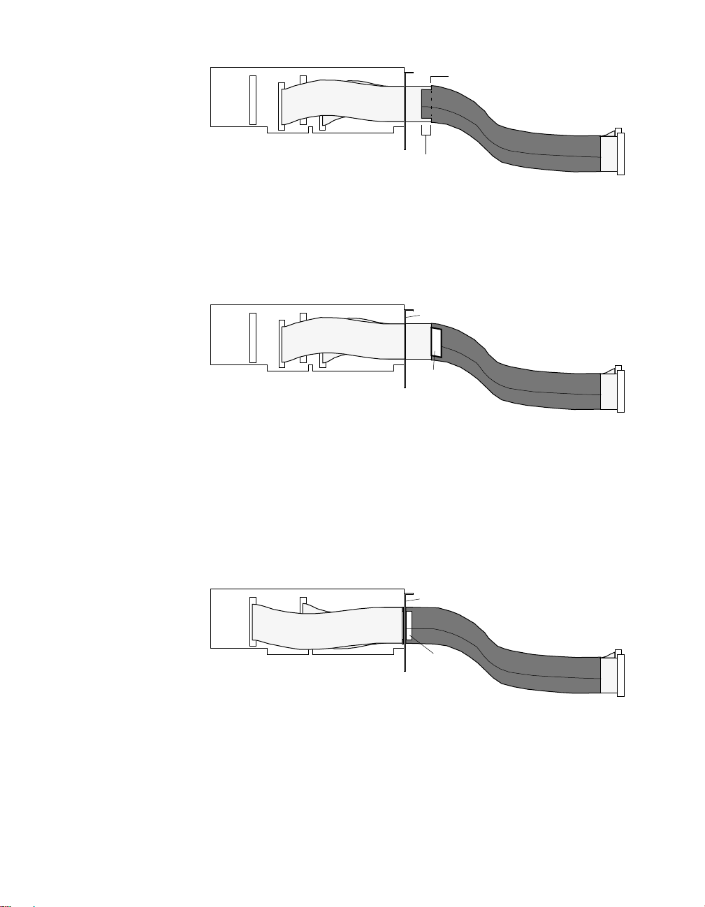
Cabling Instructions for the CE Mark Configuration . . . . . . . . C-3
Index
Page 10

List of Figures
Figure 2-1. Block Diagram of a PIO-SSR-24 . . . . . . . . . . . . 2-1
Figure 2-2. Block Diagram of PIO-SSR-48 . . . . . . . . . . . . . 2-2
Figure 2-3. Block Diagram of PIO-SSR-120 . . . . . . . . . . . . 2-3
Figure 3-1. Switch and Jumper Locations . . . . . . . . . . . . . . . 3-6
Figure 3-2. Base-Address Switch Values . . . . . . . . . . . . . . . 3-7
Figure 3-3. Jumper Block for Selection of IRQ Level . . . . . 3-8
Figure 3-4. Cable Clamp on a Mounting Plate . . . . . . . . . . 3-10
Figure 3-5. Cabling in Place . . . . . . . . . . . . . . . . . . . . . . . . 3-11
Figure 3-6. Cable Clamp Securing Single Cable . . . . . . . . . 3-11
Figure 3-7. Cabling Taped to Show Shield Boundary . . . . 3-12
Figure 3-8. Cabling Wrapped with Jacket to
Tape Boundary . . . . . . . . . . . . . . . . . . . . . . . . . 3-12
Figure 3-9. Jacket Trimmed with Scissors to Make
½
-Inch Flaps . . . . . . . . . . . . . . . . . . . . . . . . . . . 3-13
Figure 3-10. Jacket with Flaps Folded Back to Expose
Shield Surface . . . . . . . . . . . . . . . . . . . . . . . . . . 3-13
Figure 3-11. Cabling Reconnected, Placing Shield Surface
in Line with Clamp . . . . . . . . . . . . . . . . . . . . . . 3-13
Figure 3-12. Detail of Clamped Cable Showing
Installed Jacket . . . . . . . . . . . . . . . . . . . . . . . . . 3-14
Figure 4-1. Connecting an STP-50 to a PIO-SSR Series
Board . . . . . . . . . . . . . . . . . . . . . . . . . . . . . . . . . . 4-1
Figure 4-2. Connecting Two STP-50s to a PIO-SSR Series
Board . . . . . . . . . . . . . . . . . . . . . . . . . . . . . . . . . . 4-2
Figure 4-3. Connecting a PB-24 or PB-24SM to a
PIO-SSR Series Board . . . . . . . . . . . . . . . . . . . . 4-2
Figure 4-4. Connecting Two PB-24 or PB-24SM
Accessories to a PIO-SSR Series Board . . . . . . . 4-3
Figure 4-5. Contact-Closure Monitoring at an Input of a
PIO-SSR Series Board . . . . . . . . . . . . . . . . . . . . 4-4
Figure 4-6. Bounce Circuit for an Input of a PIO-SSR
Series Board . . . . . . . . . . . . . . . . . . . . . . . . . . . . 4-4
Figure 4-7. NPN Transistor Relay Control for an Output
of a PIO-SSR Series Board . . . . . . . . . . . . . . . . . 4-5
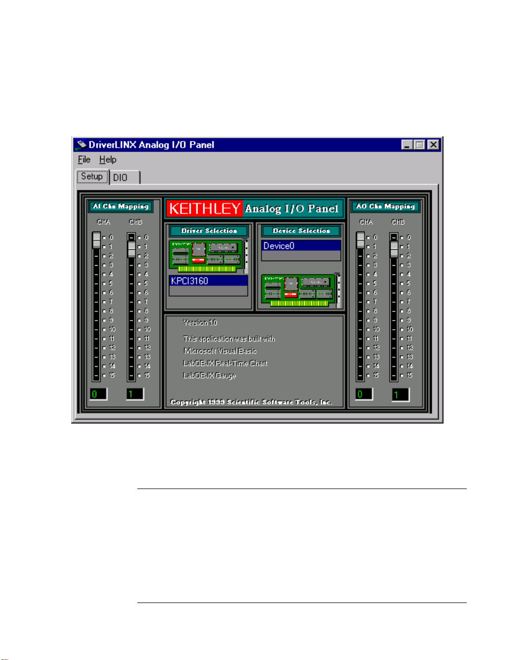
Figure 5-1. An AIO Panel example . . . . . . . . . . . . . . . . . . . . 5-2
Figure 5-2. DIO channel tab example . . . . . . . . . . . . . . . . . . 5-3
Figure 5-3. Configuring the digital I/O channels as inputs
and outputs . . . . . . . . . . . . . . . . . . . . . . . . . . . . . 5-5
Figure 5-4. Configuring channel 0 for output bit
pattern A . . . . . . . . . . . . . . . . . . . . . . . . . . . . . . . 5-5
Figure 5-5. An AIO Panel example . . . . . . . . . . . . . . . . . . . . 5-7
iii
Page 11

Figure 5-6. Configuring the digital I/O channels as
inputs and outputs . . . . . . . . . . . . . . . . . . . . . . . . 5-8
Figure 5-7. Configuring channel 0 for output bit
pattern A . . . . . . . . . . . . . . . . . . . . . . . . . . . . . . . 5-8
Figure 5-8. Configuring channel 0 for output bit
pattern B . . . . . . . . . . . . . . . . . . . . . . . . . . . . . . . 5-9
Figure 6-1. Block Diagram of IRQ Circuit . . . . . . . . . . . . . 6-11
Figure B-1. Pin Assignments for I/O Connectors
J1 to J5 . . . . . . . . . . . . . . . . . . . . . . . . . . . . . . . . B-1
Figure B-2. Pin Assignments for Edge Connector on
CAB-SSR Cable . . . . . . . . . . . . . . . . . . . . . . . . . B-2
List of Tables
Table 3-1. Priorities for IRQ Levels . . . . . . . . . . . . . . . . . . 3-9
Table 6-1. I/O Address Map for a PIO-SSR-24 . . . . . . . . . . 6-8
Table 6-2. I/O Address Map for a PIO-SSR-48 . . . . . . . . . . 6-8
Table 6-3. I/O Address Map for a PIO-SSR-120 . . . . . . . . . 6-9
Table 6-4. Bit Assignments for a Control Word
Register . . . . . . . . . . . . . . . . . . . . . . . . . . . . . . . 6-10
Table 6-5. Addresses of IRQ Control Register Bits for a
PIO-SSR-24 . . . . . . . . . . . . . . . . . . . . . . . . . . . 6-12
Table 6-6. Addresses of IRQ Control Register Bits for a
PIO-SSR-48 . . . . . . . . . . . . . . . . . . . . . . . . . . . 6-12
Table 6-7. Addresses of IRQ Control Register Bits for a
PIO-SSR-120 . . . . . . . . . . . . . . . . . . . . . . . . . . 6-13
Table 7-1. Troubleshooting Information . . . . . . . . . . . . . . . 7-3
Table A-1. Digital Input/Output Specifications . . . . . . . . . . A-1
Table A-2. Interrupt Request Specifications . . . . . . . . . . . . . A-1
Table A-3. Input Parameter Specifications . . . . . . . . . . . . . . A-2
Table A-4. Output Parameter Specifications . . . . . . . . . . . . A-2
Table A-5. General Specifications . . . . . . . . . . . . . . . . . . . . A-2
iv
Page 12

Preface
The
PIO-SSR Series User’s Guide
for handling and using PIO-SSR-24, PIO-SSR-48, and PIO-SSR-120
boards. Unless this guide refers specifically to one or more of these
models, it refers collectively to all models as the PIO-SSR Series.
To follow the information and instructions contained in this manual, you
must be familiar with data-acquisition principles, with your application,
and with an IBM PC AT
®
(or equivalent) in the MS DOS® or Windows
environments. The software that accompanies each board is compatible
with Windows 95/98 and Windows NT.
The
PIO-SSR Series User’s Guide
Section 1 provides an overview of the hardware and descriptions of
●
features, applications, supporting software, and accessories.
●
Section 2 provides a block diagram and descriptions of major
features.
Section 3 describes how to unpack, configure, and install the board
●
and how to install the software.
contains information and instructions
is organized as follows:
●
Section 4 describes how to connect accessories and circuits.
●
Section 5 describes how to start up and use the DriverLINX AIO
Panel test program; you use this utility to test your board.
Section 6 describes the I/O registers and programming options for the
●
board.
Section 7 describes how to isolate common problems, how to
●
troubleshoot your system, and how to obtain technical support.
Appendix A contains specifications.
●
●
Appendix B contains pin assignments for the I/O connectors.
●
An index completes the manual.
v
Page 13

1
Overview
PIO-SSR Series boards are multi-channel, parallel, digital I/O devices.
The boards feature high-current-driver, programmable, TTL-level I/O
channels to provide a flexible interface for SSR (solid-state relay)
modules and for a variety of parallel I/O devices, including instruments,
displays, and user-assembled systems. The PIO-SSR-120 is a
120-channel board, the PIO-SSR-48 a 48-channel board, and the
PIO-SSR-24 a 24-channel board. Each of these boards fits an expansion
slot of an IBM PC AT or equivalent. This section describes the features,
applications, supporting software, and accessories for this series of
boards.
The PIO-SSR Series boards and computer with DriverLINX software
require:
●
an IBM PC or compatible (386, or Pentium CPU) with minimum of
2 MB of memory
at least one floppy disk drive, and one fixed disk drive
●
●
Microsoft Windows 95/98, or Windows NT 4.0 or higher
●
a compiler supporting Microsoft Windows development
a mouse is highly recommended
●
1-1
Page 14

Features
Major features of PIO-SSR Series boards are as follows:
Each group of 24 digital I/O lines terminates in an onboard, 50-pin
●
header whose pin assignments are compatible with industry-standard
PB-24 and PB-24SM solid-state-relay baseboards.
Three board versions are available to drive one, two, or five PB-24
●
baseboards from a single expansion slot of your computer.
Each group of 24 digital I/O channels emulates Mode 0 of an Intel
●
8255, allowing most of the current application software for data
acquisition to work seamlessly with PIO-SSR Series boards.
●
All boards power up with all lines configured as inputs and pulled
high.
All boards provide high-current-drive capability.
●
All boards provides flexible interrupt capability.
●
●
An onboard 10kΩ pull-up resistor connected between each channel
and the +5V gives CMOS compatibility for TTL signals.
●
The software that accompanies each board is compatible with
Windows 3.x and Windows 95.
●
All PIO-SSR Series boards are ⅔ size.
Applications
Typical applications of PIO-SSR Series boards are as follows:
Machine control
●
Process monitoring and control
●
●
Control of solenoids, pumps, motors, and others
●
Contact-closure monitoring
1-2 Overview
Page 15

Supporting Software
The following software is available for operating PIO-SSR boards:
PIO-SSR standard software package —
●
Shipped with PIO-SSR
boards. Includes DriverLINX for Microsoft Windows 95/98 or
Windows NT and function libraries for writing application programs
under Windows in a high-level language such as Microsoft Visual
C++, Microsoft Visual Basic; Borland Delphi support files;
LabVIEW; utility programs; and language-specific example
programs.
DriverLINX —
●
the high-performance real-time data-acquisition
device drivers for Windows application development including:
–
DriverLINX API DLLs
and drivers supporting the PIO-SSR
hardware
–
AIO Panel —
A DriverLINX program that verifies the installation
and configuration of DriverLINX to your PIO-SSR board and
demonstrates several virtual bench-top instruments
–
Learn DriverLINX —
an interactive learning and demonstration
program for DriverLINX that includes a Digital Storage
Oscilloscope
–
Source Code —
–
DriverLINX Application Programming Interface files —
for the sample programs
PIO-SSR compiler
for the
–
DriverLINX On-line Help System —
provides immediate help as
you operate DriverLINX
–
Supplemental Documentation —
on DriverLINX installation and
configuration; analog and digital I/O programming; counter/timer
programming; technical reference; and information specific to the
PIO-SSR hardware.
PIO-SSR Series utilities —
●
The following utilities are provided as
part of the PIO-SSR Series standard software package:
– Test Utility
Supporting Software 1-3
Page 16

Accessories
The following accessories are available for use with a PIO-SSR Series
board:
●
PB-24
— A 24-channel baseboard for standard-size SSR modules.
PB-24SM
●
— A 24-channel baseboard for miniature SM Series SSR
modules.
Solid State Relay Modules
●
— Refer to Keithley’s Products catalog
for module choices and descriptions.
●
CAB-SSR
— A 3-foot ribbon cable for connecting a PIO-SSR Series
board to a PB-24 or PB-24SM accessory.
CACC-2000
●
— A 2-foot ribbon cable for connecting a PIO-SSR
Series board to an STP-50 accessory.
●
STP-50
— Universal screw-terminal panel with a 50-pin male
header.
●
Jacket
— Zipper-style shielded tubing available by the foot for
shielding flat cables; this shielding is designated
length or
Jacket nn
for custom-cut lengths (refer to the Keithley’s
Products catalog for more information).
Jacket
for a 2-foot
1-4 Overview
Page 17
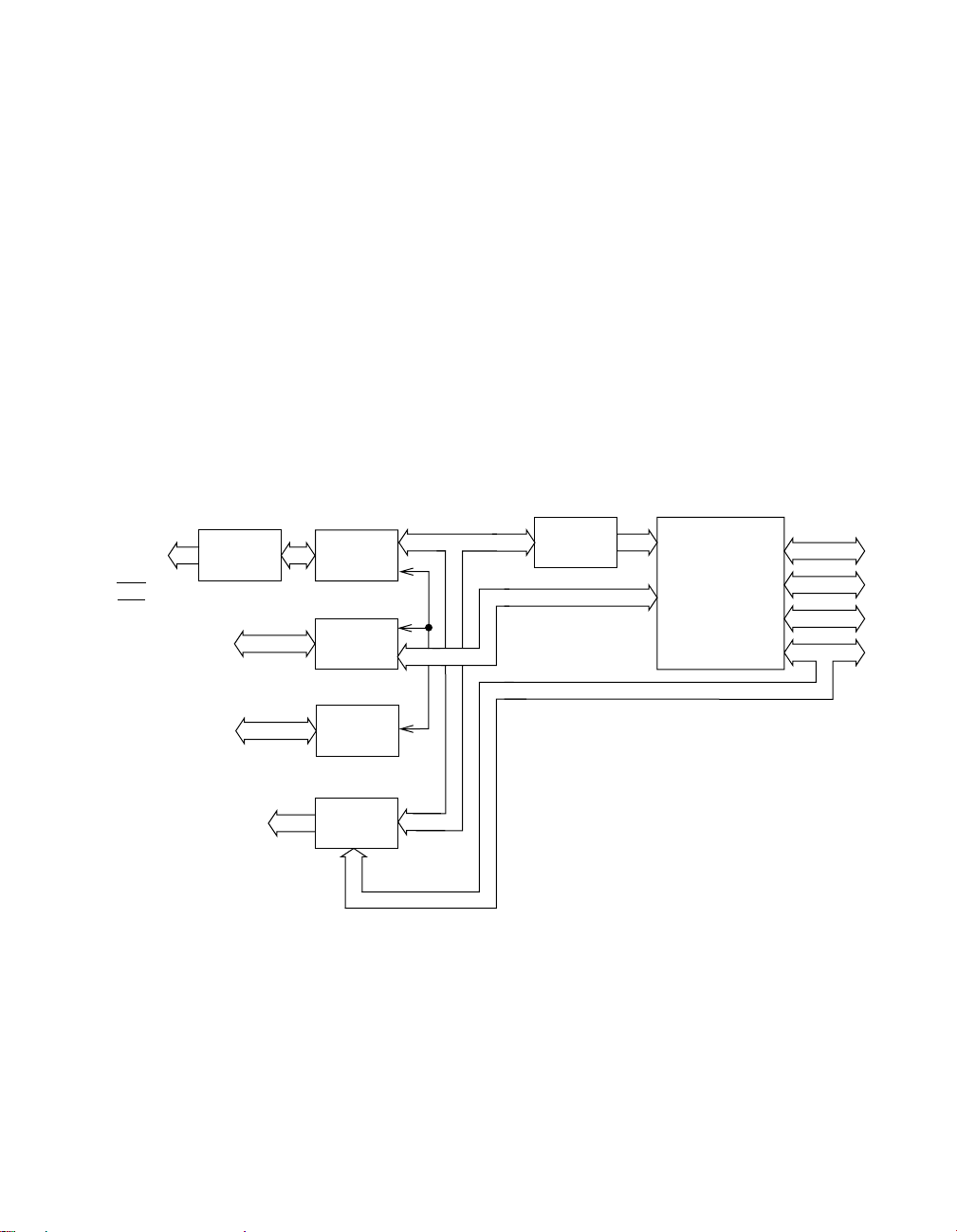
Functional Description
This section describes the features and operating characteristics of
PIO-SSR Series boards. Figure 2-1 shows a block diagram of a
PIO-SSR-24; Figure 2 -2 shows a block diagram of a PIO-SSR-48;
Figure 2-3 shows a block diagram of a PIO-SSR-120.
2
SA4
to
SA0
RESET
IOW
IOR
D7 to D0
SA15
to
SA5
IRQ
3 to 7
9 to 12
14, 15
Control
Bus
Buffer
I/O
Control
Circuit
Data
Bus
Buffer
Address
Decoder
IRQ
Control
Circuit
Control Bus
Data Bus
J1
I/O Mode
Selector
C0 and C3
Figure 2-1. Block Diagram of a PIO-SSR-24
J1 Data Buffer
Port A
Port B
Port C
A0 to A7
B0 to B7
C4 to C7
C0 to C3
2-1
Page 18
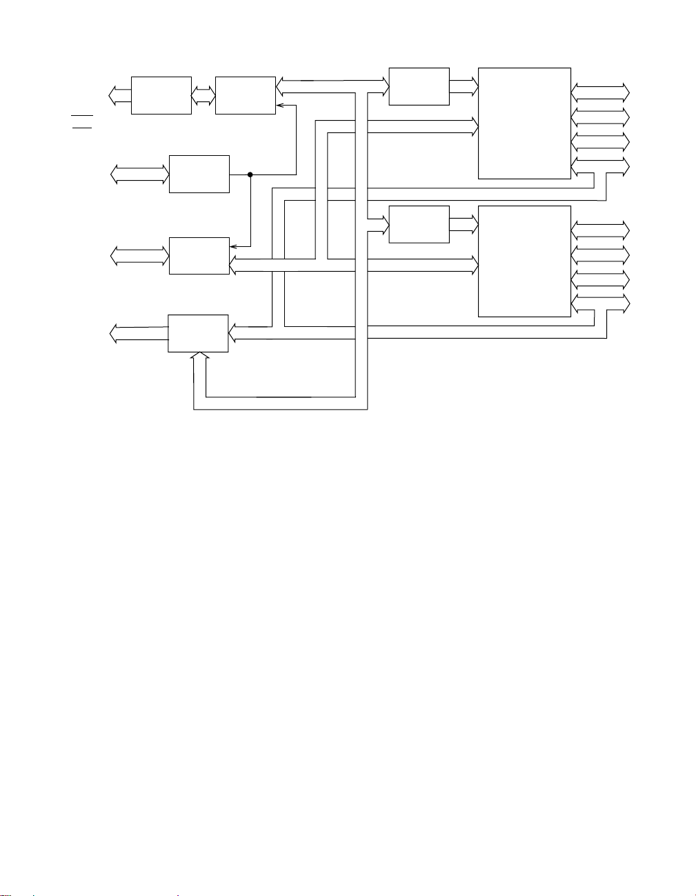
SA4
to
SA0
RESET
IOW
IOR
SA15
to
SA5
D7 to D0
IRQ
Levels
3 to 7
9 to 12
14, 15
Control
Bus
Buffer
Address
Decoder
Data
Bus
Buffer
IRQ
Control
Circuit
I/O
Control
Circuit
Control Bus
Data Bus
I/O Mode
Selector
I/O Mode
Selector
Figure 2-2. Block Diagram of PIO-SSR-48
J1
C0 and C3
J2
C0 and C3
J1 Data Buffer
Port A
Port B
Port C
J2 Data Buffer
Port A
Port B
Port C
A0 to A7
B0 to B7
C4 to C7
C0 to C3
A0 to A7
B0 to B7
C4 to C7
C0 to C3
2-2 Functional Description
Page 19

SA4
to
SA0
RESET
IOW
IOR
SA15
to
SA5
D7 to D0
IRQ
Levels
3 to 7
9 to 12
14, 15
Control
Bus
Buffer
Address
Decoder
Data
Bus
Buffer
IRQ
Control
Circuit
I/O
Control
Circuit
Control Bus
Data Bus
J1
I/O Mode
Selector
C0 and C3
J2
I/O Mode
Selector
C0 and C3
J3
I/O Mode
Selector
J1 Data Buffer
Port A
Port B
Port C
J2 Data Buffer
Port A
Port B
Port C
J3 Data Buffer
Port A
Port B
A0 to A7
B0 to B7
C4 to C7
C0 to C3
A0 to A7
B0 to B7
C4 to C7
C0 to C3
A0 to A7
B0 to B7
C0 and C3
J4
I/O Mode
Selector
C0 and C3
J5
I/O Mode
Selector
C0 and C3
Figure 2-3. Block Diagram of PIO-SSR-120
Port C
J4 Data Buffer
Port A
Port B
Port C
J5 Data Buffer
Port A
Port B
Port C
C4 to C7
C0 to C3
A0 to A7
B0 to B7
C4 to C7
C0 to C3
A0 to A7
B0 to B7
C4 to C7
C0 to C3
2-3
Page 20

Functional features of a PIO-SSR Series board are described as follows:
●
Using software, you can set each port as an input or an output.
The capacity of each channel (when set as an output) is 24mA of sink
●
current or 15mA of source current, allowing a board to drive
industry-standard solid-state relays. The SSRs allow up to 4000V
rms
of isolation and AC or DC voltage sensing up to 240V.
●
All channels in all ports are TTL-compatible and are not electrically
isolated from external circuits.
●
Channels on any PIO-SSR Series board are structured in groups of
24; a PIO-SSR-24 contains one 24-channel group, a PIO-SSR-48
contains two 24-channel groups, and a PIO-SSR-120 contains five
24-channel groups.
Each 24-channel group is accessible through an onboard, 50-pin,
●
male connector whose pin assignments are compatible with the
industry-standard PB-24 and PB-24SM solid-state-relay-module
baseboards.
●
Each 24-channel group emulates the Mode 0 operation of the Intel
8255A PPI (Programmable Peripheral Interface) integrated circuit.
● A single group comprises three 8-channel ports whose designations
are Port A, Port B, and Port C.
● While Port A and Port B are each used as 8-channel ports, Port C is
used as one 8-channel port or two 4-channel ports.
● Input channels C0 and C3 of every Port C on a board can each
generate an interrupt request (IRQ) signal for gating into a single,
jumper-selectable IRQ level.
● The IRQ levels supported by PIO-SSR Series boards are 3 to 7, 9 to
12, 14, and 15.
● The input requirement for an interrupt is the rising edge of a
TTL-compatible input signal.
● You can disable the interrupts through software.
2-4 Functional Description
Page 21

Setup and Installation
This section describes how to unwrap and inspect your board, install the
software, configure your board, create a configuration file, install the
board cabling, and install your board in the computer. These tasks are
described in the subsections that follow.
Unpacking and Inspecting a Board
After removing the wrapped board from its outer shipping carton,
proceed as follows:
1. Your PIO-SSR Series board is packaged at the factory in an anti-static
wrapper that must not be removed until you have discharged any
static electricity by either of the following methods:
3
– If you are equipped with a wrist grounding strap, you discharge
static electricity as soon as you hold the wrapped board.
– If you are not equipped with a wrist grounding strap, discharge
static electricity by holding the wrapped board in one hand while
placing your other hand firmly on a metal portion of the computer
chassis (your computer must be turned off, but grounded).
2. Carefully unwrap the board from its anti-static wrapping material.
(Store the wrapping material for future use.)
3. Inspect the board for signs of damage; if damage is apparent, return
the board to the factory. (See Technical Support on page 7-6).
4. Check the contents of your package against the packing list; report
any missing items to the factory immediately.
5. If inspection is satisfactory, proceed to install the software.
Unpacking and Inspecting a Board 3-1
Page 22

Installing and Configuring DriverLINX
Important: As a precaution against a system crash the first time you
install and test any new hardware, you should exit all other programs and,
if you use a disk cache, disable write caching. If the system does crash
and you re using disk compression software or a disk cache utility, as a
precaution after any crash, run the utility that checks the directory
structures.
Important: Before you begin installing any hardware or software for the
PIO-SSR, read the DriverLINX Installation and Configuration Guide and
the Using DriverLINX with your Hardware Keithley PIO Series
manuals that are packaged with the DriverLINX software. They are
accessed from the DriverLINX CD-ROM after you have installed Adobe
Acrobat.
Before Installing DriverLINX
1. Inventory your PIO-SSR board’s configuration settings.
2. Determine the resources your PIO-SSR board requires.
3. Inventory your computer’s resources already allocated to other
installed devices.
4. Determine whether your computer has sufficient resources for your
PIO-SSR board.
5. Determine whether your PIO-SSR board can use your computer’s
free resources.
6. Set any jumpers/switches to configure your PIO-SSR board to use
your computer’s free resources.
7. Set any other jumpers/switches to configure your PIO-SSR board as
desired.
3-2 Setup and Installation
Page 23

Selecting the DriverLINX Components to Install
For your convenience in installing and un-installing just the DriverLINX
components you need, the DriverLINX CD Browser will assist you in
selecting the components to install:
● Install Drivers — This required component installs only the files you
need for configuring your hardware and running third-party
data-acquisition applications that require DriverLINX.
● Install Interfaces — This optional component installs the files and
example programs that you will need to develop custom applications
for DriverLINX using C/C++, Visual Basic, Delphi, and LabVIEW.
● Install Documentation — This optional component installs
electronic documentation for DriverLINX that you can read, search,
and print using the Adobe Acrobat Reader.
● Install Acrobat — This optional component installs the Adobe
Acrobat Reader for the DriverLINX electronic documentation.
Installing DriverLINX
1. Insert the DriverLINX CD-ROM into your computer’s CD-ROM
Drive.
2. Start the DriverLINX setup program. On most systems, wait a few
seconds for automatic startup. Otherwise, run the setup.exe program
from the CD-ROM.
3. The DriverLINX CD-ROM Browser Map window appears on the
screen. Click Install Drivers, and follow the series of on-screen
instructions.
Note: To display an explanation of a menu option on the DriverLINX CD
browser map that appears next and on subsequent setup screens, place the
mouse pointer over the menu item. A star next to a menu item means that
the item was selected previously.
4. Select Read Me First, and follow the instructions.
Installing and Configuring DriverLINX 3-3
Page 24

5. Select Install Documentation. If you do not have Adobe Acrobat
installed on your computer, install it by selecting Install Adobe
Acrobat.
6. Open the manuals appropriate to the PIO-SSR installation and read
them before installing your PIO-SSR board or configuring
DriverLINX:
– Installation and Configuration
– Using DriverLINX with Your Hardware—Keithley PIO Series
– DriverLINX Technical Reference Manual
– DriverLINX Digital I/O Programming Guide
– DriverLINX Analog I/O Programming Guide
– DriverLINX Counter/Timer Programming Guide
– Appendix, I/O Port, Interrupt, and DMA Channel Usage
– Other manuals appropriate to your installation.
7. Before installing a PIO-SSR board in your computer, make sure that
the switches are set appropriately and that you have noted the switch
settings so that you can match these settings when you program the
configuration using DriverLINX. Refer to the DriverLINX
Installation and Configuration Guide and Using DriverLINX with
Your Hardware—Keithley PIO Series manuals.
8. Install your PIO-SSR board into an appropriate free slot in your
computer when DriverLINX prompts you to do so.
Note: If switches on the board are changed after the software has been
installed, the software will need to be reconfigured.
Refer to the documentation provided with your computer for more
information on installing boards.
Follow the DriverLINX on-screen instructions for installation of drivers
and interfaces. Refer to the DriverLINX Installation and Configuration
Guide and Using DriverLINX with Your Hardware—Keithley PIO Series
manuals.
3-4 Setup and Installation
Page 25

Note: Be sure to note and follow all programming differences between
installations for Windows NT and Windows 95/98.
Note: Typically, base addresses between 300h and 370h are available for
use. However, keep in mind that a network board, a sound board, a
CD-ROM, or other data acquisition board may use a base address within
this space.
DriverLINX allows you to set base addresses between 200h and 3F0h
only. Therefore, if you are using your PIO-SSR board with software that
requires a configuration file, you must specify an even boundary of four
I/O addresses within the range of 200h to 3F8h.
Configuring a Board
Keithley configures your PIO-SSR Series board by presetting a base I/O
address and an IRQ level. While the factory settings are suitable for most
installations, ensure these settings are not already in use by other devices
in your computer. If your board requires reconfiguration, you must set a
new base address and/or select a new IRQ level by setting the
base-address switches and IRQ-level jumper. These components are
located as shown in Figure 3-1.
Configuring a Board 3-5
Page 26
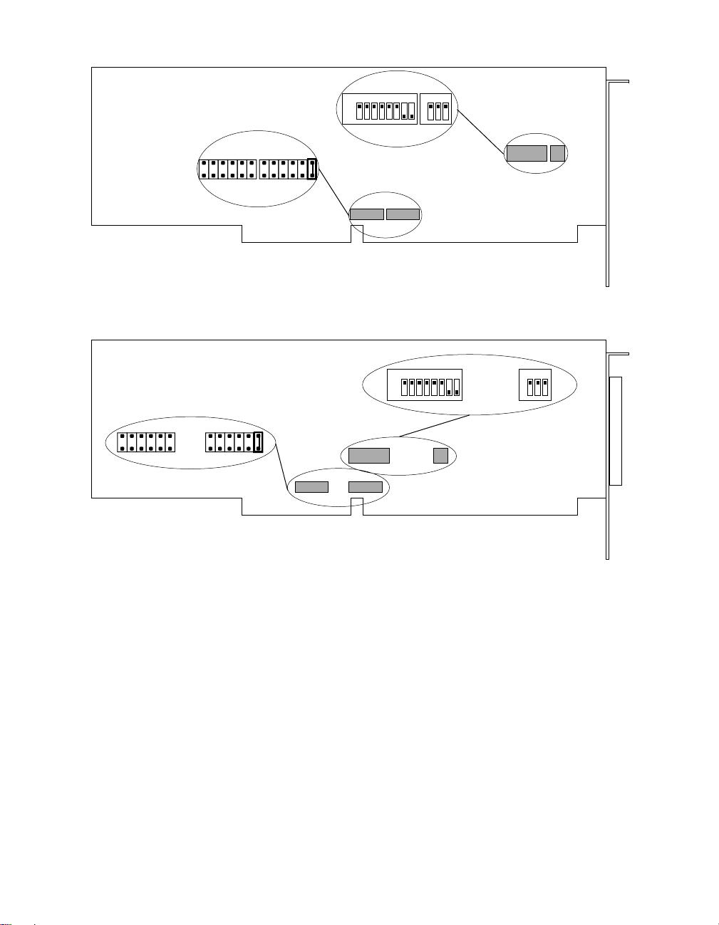
IRQ-Level Jumper
Blocks
IRQ-Level Jumper
Blocks
Base Address
Switches
PIO-SSR-24/48
Base Address
Switches
PIO-SSR-120
Figure 3-1. Switch and Jumper Locations
The following subsections describe how to set the base address and IRQ
level.
Setting the Base I/O Address
Addresses in the I/O space of your computer can range from 0000h to
FFFFh, for a total of 65,535 locations. IBM recommends a base I/O
address between 100h and 3FFh only and reserves some addresses in this
range computer and I/O device use. You can set your PIO-SSR Series
3-6 Setup and Installation
Page 27

board for an address well beyond the 100h to 3FFh range; Keithley
recommends *300h, *700h, *B00h, or *F00h (where * is any number in
the range of 0 to Fh) as valid base I/O addresses. You can also assign your
board an address that is 400h, 800h, or C00h above the upper limit of
3FFh recommended by IBM.
Caution: Writing to a base I/O address above 400h can sometimes draw
response from a device using an address below 400h. For example, an
address of 01F0h is used by many computers for a fixed disk. If the disk
drive controller board sees only the 10 least significant address lines (A0
to A9), then writing to 1F0h, 5F0h, 9F0h, or DF0h could inadvertently
activate the disk drive controller board.
The base-address switches are preset at the factory for a default base I/O
address of 300h (the address reserved by many computers for a prototype
board). If this address is already assigned to another device in your
computer, reset the switches for a different I/O address. Use the
information shown in Figure 3-2 to determine settings for a new address.
Hexadecimal V alue
Decimal Value
Computer
Address Line
Switch settings indicate a base address of
800
1000
2000
4000
8000
2048
4096
8192
16384
32768
A15
A14
A13
A12
A11
O
N
1 2 3 4 5 6 7 8
Switch 1
100
200
400
256
512
1024
A9
A10
512 + 256 = 768 Decimal
200h + 100h = 300h
A8
O
N
or
80
64
128
A7
A6
Switch 2
1 2 3
A5 32
20
40
Figure 3-2. Base-Address Switch Values
Configuring a Board 3-7
Page 28

Note: A base I/O address switch has value only when set to its OFF
position.
Notice that the least significant address line in Figure 3-2 is A5. This line
has a decimal value of 32; therefore, the address you select is on a 32-byte
boundary, giving the board access to 32 I/O address ports (the board
actually uses a maximum of only 22 address ports, as shown in the I/O
address maps of Section 6).
Setting the IRQ Level
A PIO-SSR Series board can generate an IRQ signal on the rising edge of
any input signal from either the C0 or C3 input channel. To gate the IRQ
signal to your computer, you must place a jumper on one of the IRQ-level
settings of the jumper block. The IRQ-level options on the jumper block
are 3 to 7, 9 to 12, 14, and 15. The jumper block also contains a position
labelled X for no connection. Your board is preset at the factory for the X
position, as shown in Figure 3-3.
9 3 4 5 6 7 10 11 12 14 15 X
Figure 3-3. Jumper Block for Selection of IRQ Level
3-8 Setup and Installation
Page 29

Priorities for the IRQ levels are shown in Table 3-1.
Table 3-1. Priorities for IRQ Levels
Priority IRQ Level
First 9
Second 10
Third 11
Fourth 12
Fifth 14
Sixth 15
Seventh 3
Eighth 4
Ninth 5
Tenth 6
Eleventh 7
Configuring a Board 3-9
Page 30

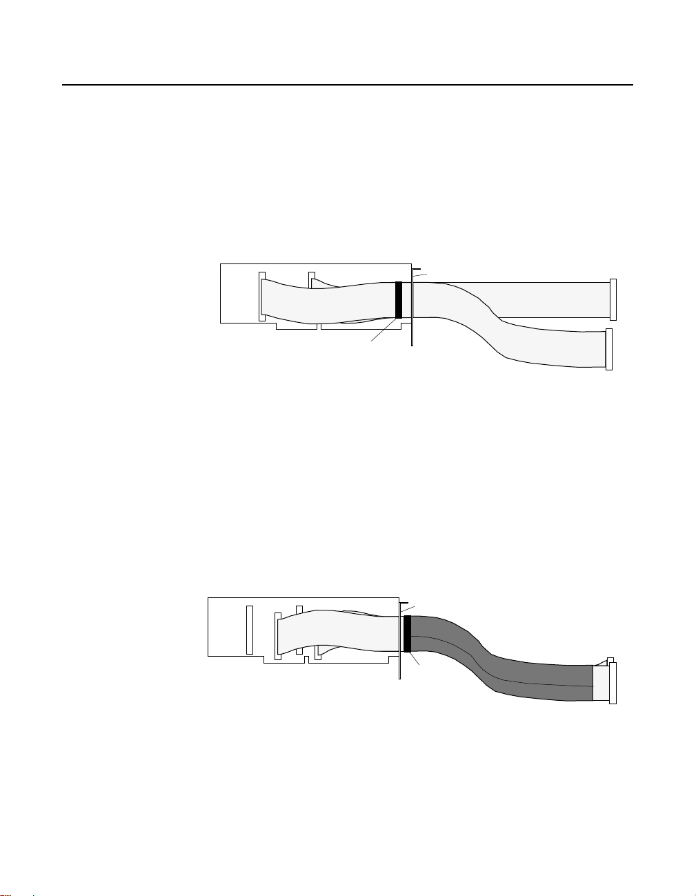
Clamping Cables to the Board
The mounting plate of your PIO-SSR Series board contains an adjustable
cable clamp that can secure up to five flat cables (shown in Figure 3-4
with a single cable).
Board
Mounting Plate
of Board
Clamp Adjusting
Screw
Cable Clamp
Clamp Adjusting
Screw
Figure 3-4. Cable Clamp on a Mounting Plate
To clamp one or more cables to your board, use the following procedure:
1. Remove the two clamp-adjusting screws and the clamp from the
board’s mounting plate.
2. Feed a cable through the hole in the mounting plate, and plug the
cable connector into the I/O connector nearest the mounting plate (if
your board contains more than one I/O connector).
3-10 Setup and Installation
Page 31

3. If your board is using more than one cable, feed the next cable
through the hole in the mounting plate, and plug the cable connector
into the next available I/O connector.
4. Repeat step 3 until all cables are in place on the board, as shown in
Figure 3-5.
PIO-SSR-48
Figure 3-5. Cabling in Place
5. Re-install the clamp and clamp-adjusting screws so that the clamp
holds the cabling firmly in place, as shown in Figure 3-6.
Mounting Plate
of Board
Clamp Adjusting
Screw
Cable
Cable Clamp
Clamp Adjusting
Screw
Figure 3-6. Cable Clamp Securing Single Cable
Clamping Cables to the Board 3-11
Page 32
Installing Cable Shielding
To shield cabling for your PIO-SSR Series board, perform the
following steps:
1. With cabling installed and clamped, wrap all cables together with a
piece of tape to mark a shield boundary at a point ½-inch or more
away from the inside surface of the mounting plate, as shown in
Figure 3-7.
PIO-SSR-48
Tape Marker ½ inch
from Mounting Plate
Figure 3-7. Cabling Taped to Show Shield Boundary
Mounting Plate
2. Remove the two clamp-adjusting screws and the clamp from the
board’s mounting plate.
3. Unplug the cable connectors from the board, and pull the taped
cabling back through the mounting plate until the tape marker is
beyond the clamping area.
4. Beginning at the tape marker, cover the cabling with a single piece of
jacket to the desired length, as shown in Figure 3-8.
PIO-SSR-48
Mounting Plate
Tape
Figure 3-8. Cabling Wrapped with Jacket to Tape Boundary
5. Remove tape from cabling, and use scissors to cut ½-inch flaps in the
jacket on both sides of cable, as shown in Figure 3-9.
3-12 Setup and Installation
Page 33
PIO-SSR-48
½ inch
Fold Line
Figure 3-9. Jacket Trimmed with Scissors to Make ½-Inch Flaps
6. Fold the flaps back on both sides of the cabling to expose the shield
surface, as shown in Figure 3-10.
PIO-SSR-48
Mounting Plate
Shield
Surface
Figure 3-10. Jacket with Flaps Folded Back to Expose Shield
Surface
7. Slide cabling back through the mounting plate and plug the cable
connectors back into the board, placing shield surface directly in line
with mounting-plate clamp, as shown in Figure 3-11.
PIO-SSR-48
Mounting Plate
Shield
Surface
Figure 3-11. Cabling Reconnected, Placing Shield Surface in Line
with Clamp
Installing Cable Shielding 3-13
Page 34
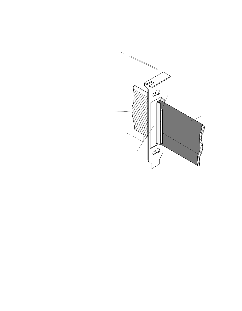
8. Re-install the clamp and clamp-adjusting screws so that the clamp
holds the cabling firmly in place while bearing firmly on the shield
surface of the jacket flap, as shown in Figure 3-12.
Trimmed and
Folded-back
Jacket Flap
Cable
Clamp
Jacket
over
Cable
Figure 3-12. Detail of Clamped Cable Showing Installed Jacket
Note: This shielding procedure assures CE Mark compliance (refer to
Appendix C for more information).
3-14 Setup and Installation
Page 35

Installing a Board
Caution: Installing or removing a board while power is ON can damage
your computer.
Use the following steps to install a PIO-SSR Series board in an expansion
slot of your computer:
1. Turn off power to the computer and all attached equipment.
2. Remove the computer chassis cover.
3. Select an unoccupied expansion slot in the rear panel, and remove the
corresponding dummy mounting plate.
4. Ensure the settings of the base-address switch and the IRQ jumper
match the settings shown in the configuration utility.
5. Insert and secure the board in the selected expansion slot, feeding any
cable ends through the rear panel of the computer as you insert the
board.
6. Replace the computer cover.
You can use the AIO Panel (Section 5) to check board operation.
You are now ready to make I/O connections. Refer to Section 4 for
descriptions of I/O accessories and connections for a PIO-SSR Series
board.
Installing a Board 3-15
Page 36

Configuring DriverLINX
After you have successfully installed the PIO-SSR board in your
computer, start Windows to install DriverLINX. For detailed instructions
on installing DriverLINX, see the documentation provided on the
DriverLINX CD-ROM. Refer to the DriverLINX Installation and
Configuration Guide and Using DriverLINX with Your
Hardware—Keithley PIO Series manuals.
Caution: Be sure to note and follow differences in programming
between Windows NT and Windows 95/98 as appropriate for your
system.
Run Learn DriverLINX (LearnDL.exe) from the DriverLINX program
group to tell DriverLINX how you configured your PIO-SSR board and to
verify that everything is properly installed and configured.
1. Start Windows as you normally would and select the Program
Manager window. Install DriverLINX if you have not previously
done so.
2. Either select the Learn DriverLINX icon created when you installed
DriverLINX or enter <drive>:/DRVLNX/LEARNDL in the
Command Line edit box. The command line edit box is activated by
selecting the Run... option. <drive> is the letter of the hard disk drive
where DriverLINX is installed.
3. Immediately after loading Learn DL, the Open DriverLINX DLL
dialog box appears. Select the name of the hardware-specific DLL
from the list for your PIO-SSR board. The name is an abbreviation of
the board’s model number.
4. From the main menu bar of Learn DL, select the Device menu and
choose Select....
5. Select the Logical Device you wish to configure and then click on the
OK button (return).
6. Again select the Device menu and then choose the Configure... option
to display the Device Configuration Dialog Box.
3-16 Setup and Installation
Page 37

7. From the Model list, select the model name for the PIO-SSR board
you are configuring.
8. If the value displayed in the Address edit box is not correct, type the
correct value into the box. You may enter the address in decimal or
hexadecimal using the c-notation for hex (that is, 768 decimal =
0x300 hexadecimal).
9. Choose the correct options for the Analog, Digital, and
Counter/Timer Sections by first clicking on the appropriate radio
button in the middle of the dialog box and then completing the group
of dialog fields in the lower third of the dialog box. Be sure to click on
both the Input and Output radio buttons for the Analog and Digital
groups to see all the dialog fields.
10. After you have made your selections, save the configuration
parameters by clicking on the OK button.
11. Repeat the preceding steps, starting at step 5, for each Logical Device
you want to configure.
Configuring DriverLINX 3-17
Page 38
4
Cabling and Wiring
This section describes the cabling and wiring required for attaching
accessories and field devices to the I/O connectors of your PIO-SSR
Series board. The board contains one I/O connector for each group of 24
channels; thus, the PIO-SSR-24 contains one I/O connector, the
PIO-SSR-48 contains two I/O connectors, and the PIO-SSR-120 contains
five I/O connectors. Pin assignments for an I/O connector are shown in
Appendix B.
Caution: To avoid electrical damage, turn off power to the computer and
any accessories before making connections to a PIO-SSR Series board.
Shorting any output of a PIO-SSR Series board to +5V or ground can
damage the board.
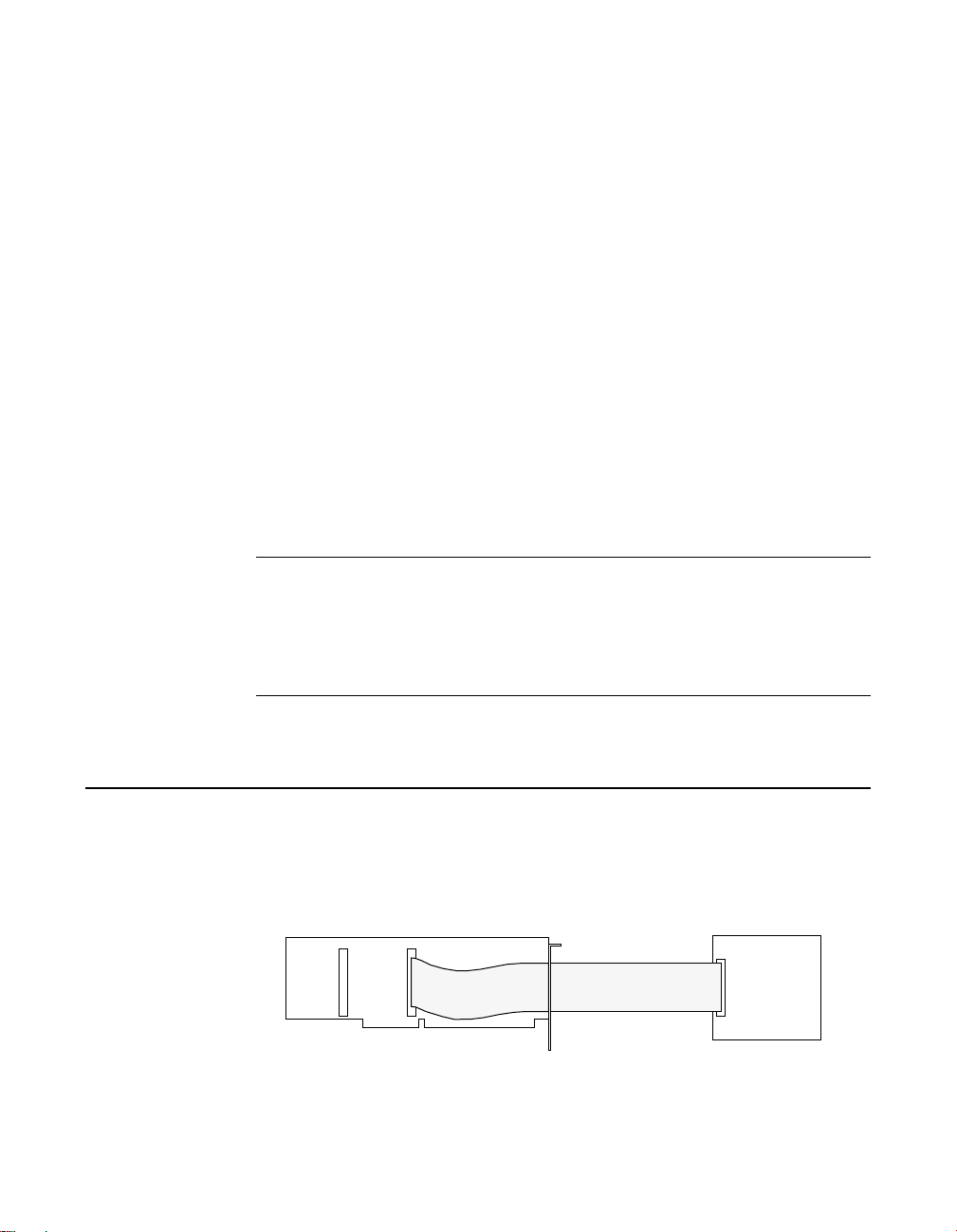
Connecting an STP-50
An STP-50 connects to an I/O connector of a PIO-SSR Series board as
shown in Figure 4-1.
PIO-SSR-48
STP-50
Accessory
CACC-2000
Cable
Figure 4-1. Connecting an STP-50 to a PIO-SSR Series Board
Connecting an STP-50 4-1
Page 39

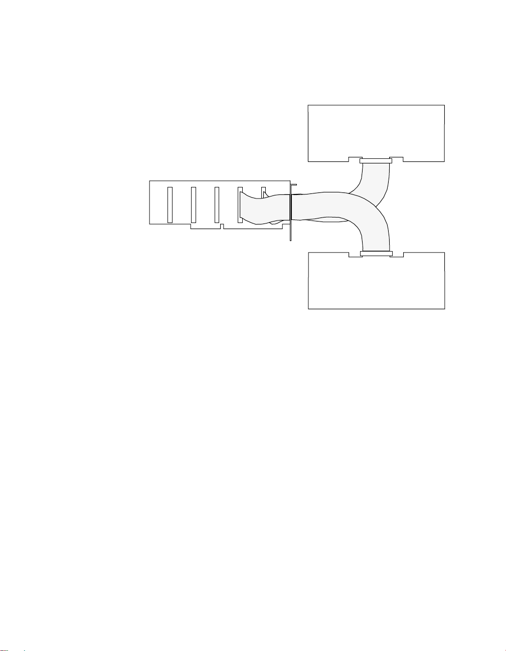
Two STP-50 accessories connect to I/O connectors of a PIO-SSR Series
board as shown in Figure 4-2.
PIO-SSR-48
Figure 4-2. Connecting Two STP-50s to a PIO-SSR Series Board
Connecting a PB-24 or PB-24SM
CACC-2000
Cables
STP-50
Accessory
STP-50
Accessory
A PB-24 or PB-24SM connects to an I/O connector of a PIO-SSR Series
board as shown in Figure 4-3. Refer to Appendix B for pin assignments
versus relay connections.
PB-24 or
PIO-SSR-120
CAB-SSR Cable
Figure 4-3. Connecting a PB-24 or PB-24SM to a PIO-SSR Series
Board
4-2 Cabling and Wiring
PB-24SM
Baseboard
Page 40
You can connect two or more PB-24 or P-24SM baseboards to I/O
connectors of a PIO-SSR Series board as shown in Figure 4-4.
PB-24 or
PB-24SM
Baseboard
PIO-SSR-120
CAB-SSR
Cables
PB-24 or
PB-24SM
Baseboard
Figure 4-4. Connecting Two PB-24 or PB-24SM Accessories to a
PIO-SSR Series Board
Connecting a PB-24 or PB-24SM 4-3
Page 41
Monitoring Contact Closure at an Input
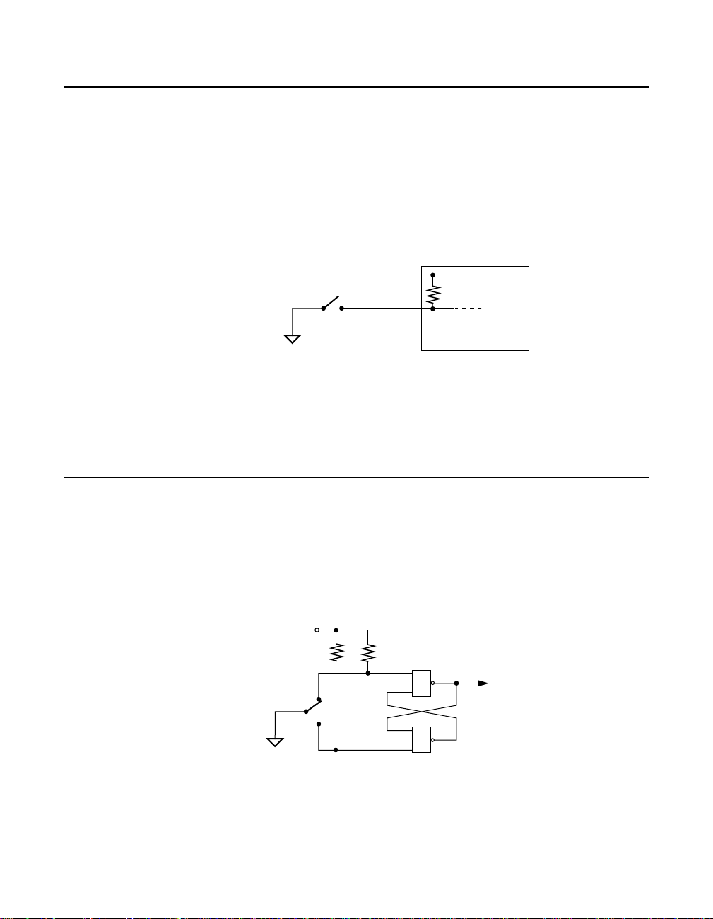
An onboard 10kΩ pull-up resistor connected between each channel and
the +5V serves to prevent floating input when contact is open and gives
CMOS compatibility for TTL signals. Figure 4-5 shows how this resistor
makes an input of a PIO-SSR Series board an effective circuit for
monitoring contact closure.
+5 V
PIO-SSR Series
n
Onboard Pull-up
Resistor
Board
10 kΩ
Switch
Digital
Common
GND
Digital
Input
#
Figure 4-5. Contact-Closure Monitoring at an Input of a
PIO-SSR Series Board
Eliminating Contact Bounce
While you can eliminate contact bounce through your application
program, you can also insert a bounce circuit between the contacts and
the input of your PIO-SSR Series board. Figure 4-6 shows a typical
bounce circuit.
+5 V
10 kΩ
10 kΩ
&
To Digital Input
of a
PIO-SSR Series
Board
&
Digital
Common
GND
Figure 4-6. Bounce Circuit for an Input of a PIO-SSR Series Board
4-4 Cabling and Wiring
TTL
Compatible
AND Gate
Page 42

Boosting Relay Drive Current
PIO-SSR Series boards can drive relays other than the standard solid-state
relays. The maximum output current for each channel of a PIO-SSR
Series board is 24mA at 5V. If your relay requires more than 24mA or
more than 5V, you can boost the drive current and/or voltage for relay
control using the circuit shown in Figure 4-7.
Digital
Output
n
PIO-SSR Series
Board
Figure 4-7. NPN Transistor Relay Control for an Output of a
#
NPN
Transistor
PIO-SSR Series Board
470 Ω
Min.
Digital
Common
GND
Relay
Surge
Protection
Diode
+
−
To Relay
DC Power
Supply
For drive-current requirements between 15mA and 100mA, select an
NPN transistor with appropriate current capacity. The power transistor
must be rated for the required supply voltage and must have a collector
current rating no higher than 0.5A. If higher current is needed, substitute a
Darlington NPN transistor.
Boosting Relay Drive Current 4-5
Page 43

I/O Bit Tests
5
Testing Your Board
You can use DriverLINX to verify board operation:
1. To physically initialize the PIO-SSR, select Device/Initialize from the
main menu in Learn DriverLINX.
2. The first time the PIO-SSR is initialized, or after a configuration
change, DriverLINX runs a diagnostic program to verify the
operation and accuracy of the configuration settings.
After you install the PIO-SSR board and configure DriverLINX for the
desired PIO-SSR configuration, you can attach an accessory board and
wire the appropriate signals to the board. Before writing your application
program, you can test the functions of the PIO-SSR board using the
DriverLINX AIO Panel test program.
General Information
1. Start the AIO Panel as follows:
a. In the Start menu, click Programs.
b. Find the DriverLINX ➧ Test Panels folder, under which you
should find the AIO Panel entry.
I/O Bit Tests 5-1
Page 44

c. Click on the AIO Panel entry. The Analog I/O Panel should
appear, similar to the example in Figure 5-1. (If you have other
DriverLINX devices installed in addition to the digital
input/output card you are testing, they will also be listed. In that
case, select the desired digital I/O card and the proper device
number before proceeding.)
Figure 5-1. An AIO Panel example
Note: The “Driver Selection” column will show the actual DriverLINX
driver(s) you have installed.
5-2 Testing Your Board
Page 45

2. On the AIO Control Panel, click the DIO tab.
Figure 5-2. DIO channel tab example
I/O Bit Tests 5-3
Page 46

Note: The on-screen digital I/O controller works as follows:
● Channels 0 to 15 refer to the 8-bit general-purpose registers of
your digital input-output card. (Depending on which card is
used, the number of valid 8-bit registers will vary.) Bits
displayed on the Digital Input Panel and the Digital Output
Panel are numbered 0-7 for every channel. Refer elsewhere in
this manual for a description of the available ports and their
direction.
● Invalid channels and settings appear as dark gray squares. For
example:
- Non-existent channels always appear as dark gray squares.
- Channels configured as inputs will appear as dark gray
squares on the output panel.
● Valid channels and settings appear as white squares when OFF
and green squares when ON. (When the manual is printed in
black and white, valid channels and settings appear as white
squares when OFF and as light gray squares when ON.)
● The two-digit numeric displays under Input Bits and Output
Bits show the hexadecimal values of the adjacent bit patterns.
● To configure a valid channel either for input or output, use the
Digital Channel Configuration Panel. Click on either the
Input or Output square below the channel number. Note: this
selection will be disabled for channels which are fixed as input
or output by hardware design.
● To turn ON output-channel bits, use the Digital Output Panel.
First select the channel number of the bits to be turned on by
clicking on the appropriate square under Channels. Then, turn
ON a bit by clicking the appropriate square under Output Bits.
Turn OFF a bit in the same way.
● To read an input-channel bit, use the Digital Input Panel. First
select the channel number to be checked by clicking the
appropriate square under Channels. Then, read the numbered
bit under Input Bits. OFF input bits appear as black dots and
ON input bits appear as green dots. (When the manual is
printed in black and white, OFF input bits appear as black dots
and ON input bits appear as light gray dots.)
5-4 Testing Your Board
Page 47

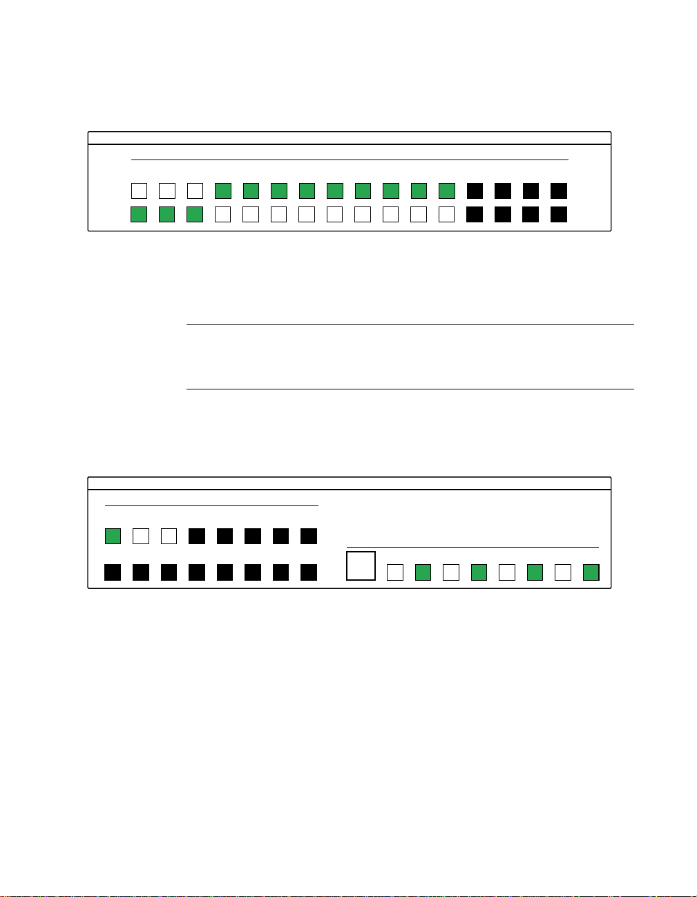
3. Under Digital I/O Configuration Panel, configure channels as
shown in Figure 5-3. (Actual channels available will vary according
to your hardware.)
KEITHLEY
Channel Configuration
0
Input
Output
123456789101112131415
Digital I/O Configuration Panel
Figure 5-3. Configuring the digital I/O channels as inputs and outputs
Note: For clarity when the manual is printed in black and white, the
control colors in Figure 5-3 and subsequent drawings will be shown as
follows:
Color on
Illustration
BLACK DARK GRAY Invalid
WHITE LIGHT GRAY OFF
GRAY GREEN ON
Actual Panel Function
4. In the Digital Output Panel under Channels, click on a channel
(here, channel 0) as shown in Figure 5-4.
KEITHLEY
Channels
1234567
0
8 9 10 11 12 13 14 15
Output Bits
765 43210
Digital Output Panel
55
Figure 5-4. Configuring channel 0 for output bit pattern A
I/O Bit Tests 5-5
Page 48

5. In the Digital Output Panel under Output Bits, set the bits of the
6. In the Digital Input Panel under Channels, click on a channel to
Output Set Test
The output set test checks whether logic levels measured at all output pins
agree with output bit patterns set by software, using a DriverLINX
graphical interface (AIO Panel).
Note: This test is performed without user circuits being connected to the
outputs.
Perform the output set test as follows:
1. Ready the following equipment:
channel as desired as shown in Figure 5-4. (Click on each bit position
to turn it ON or OFF.)
select it and display the logical state of its input lines.
● A digital voltmeter (DVM) or a digital multimeter (DMM) set to
measure voltages, or a logic probe capable of reading TTL logic
levels.
● A suitable accessory and cable for the board being tested.
2. Turn OFF the host computer.
3. Connect the cable and accessory to your board.
4. Turn ON the host computer and boot Windows 95/98/NT.
5. Click the Windows 95/98/NT Start tab.
6. Start the AIO Panel as follows:
a. In the Start menu, click Programs.
b. Find the DriverLINX ➧ Test Panels folder, under which you
should find the AIO Panel entry.
5-6 Testing Your Board
Page 49
c. Click on the AIO Panel entry. The Analog I/O Panel should
appear, similar to the example in Figure 5-5. (If you have other
DriverLINX devices installed in addition to the digital
input/output card you are testing, they will also be listed. In that
case, select the desired digital I/O card and the proper device
number before proceeding.)
Figure 5-5. An AIO Panel example
7. On the AIO Panel , click the DIO tab.
Note:
To read an input-channel bit, use the Digital Input Panel . First,
select the channel number to be checked by clicking the appropriate
square under Channels . Then, read the numbered bit under Input Bits .
OFF input bits appear as black dots and ON input bits appear as green
dots. (When the manual is printed in black and white, OFF input bits
appear as black dots and ON input bits appear as light gray dots.) Further
information about this panel, how to make changes, and how to interpret
displays, is given in “I/O Bit Tests” of this section.
I/O Bit Tests 5-7
Page 50
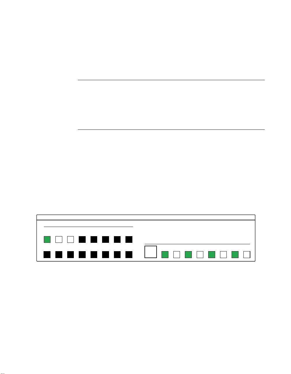
8. Under Digital I/O Configuration Panel, configure the output
channels to be tested as shown in Figure 5-6. (Actual output channels
available will vary according to your hardware.)
KEITHLEY
Channel Configuration
0
Input
Output
123456789101112131415
Digital I/O Configuration Panel
Figure 5-6. Configuring the digital I/O channels as inputs and outputs
Note: In Figure 5-6 and subsequent drawings of digital I/O controller
panels, the squares below invalid channels are colored black instead of
dark gray—for clarity when the manual is printed in black and white.
9. In the Digital Output Panel under Channels, click on an output
channel (channel 0 in this example) as shown in Figure 5-7.
KEITHLEY
Channels
1234567
0
8 9 10 11 12 13 14 15
Output Bits
765 43210
Digital Output Panel
55
Figure 5-7. Configuring channel 0 for output bit pattern A
10. In the Digital Output Panel under Output Bits, set the bits of
channel 0 for bit pattern A as shown in Figure 5-7.
11. Measure the voltage between signal ground and each bit of the output
port with a DMM or DVM. Make measurements at the cabled mating
connector of your accessory.
5-8 Testing Your Board
Page 51
12. Each bit set to ON in the AIO Panel should output a logic-high signal
at the corresponding I/O terminal, reading typically about 4 volts
(minimum of 2.2 volts) at a DMM/DVM. Each bit set to OFF in the
AIO Panel should output a logic-low signal at the corresponding I/O
terminal, reading typically about 0 volts (maximum of 0.8 volts) at a
DMM/DVM. Do one of the following:
Note: The typical values shown are valid for boards with TTL
compatible outputs. For boards with relay outputs (REL-16, PDISO-8,
and PIO-32) the output will be a relay contact closure. For boards with
open collector outputs (PIO-HV) use a pull up resistor to an appropriate
voltage to detect output state. Refer to the hardware description in this
user’s guide for more details on the output’s electrical specification.
● If the bit patterns set on the AIO Panel do not agree with the
logic levels measured at the I/O terminals, the board is not
functioning properly. Stop here, and determine why.
● If the bit patterns set on the AIO Panel agree with the logic levels
measured at the I/O terminals, then repeat steps 9, 10, and 11 for
remaining output channels.
13. In the Digital Output Panel under Channels, click on the output
channel to test (channel 0 in this example) as shown in Figure 5-8.
KEITHLEY
Channels
1234567
0
8 9 10 11 12 13 14 15
Figure 5-8. Configuring channel 0 for output bit pattern B
14. In the Digital Output Panel under Output Bits, set the bits of
channel 0 for bit pattern B as shown in Figure 5-8.
15. Measure the voltage between signal ground and each bit of the output
port with a DMM or DVM. Make measurements at the STA-50
terminals or the cabled mating connector that is connected to the
selected CONN-3160-D1 50-pin connector.
Digital Output Panel
Output Bits
76 5 43 2 1 0
AA
I/O Bit Tests 5-9
Page 52

16. Again, each bit set to ON in the AIO Panel should output a logic-
high signal at the corresponding I/O terminal, reading typically about
4 volts (minimum of 2.2 volts) at a DMM/DVM. Each bit set to OFF
in the AIO Panel should output a logic-low signal at the corresponding I/O terminal, reading typically about 0 volts (maximum of
0.8 volts) at a DMM/DVM.
Note: The typical values shown are valid for boards with TTL
compatible outputs. For boards with relay outputs (REL-16, PDISO-8,
and PIO-32) the output will be a relay contact closure. For boards with
open collector outputs (PIO-HV) use a pull up resistor to an appropriate
voltage to detect output state. Refer to the hardware description in this
user’s guide for more details on the output’s electrical specification.
● If the bit patterns set on the AIO Panel do not agree with the
logic levels measured at the I/O terminals, the board is not
functioning properly. Stop here, and determine why.
● If the bit patterns set on the AIO Panel do agree with the logic
levels measured at the I/O terminals, and you have performed an
output set test for all ports, the board is functioning properly.
17. Repeat steps 13, 14, and 15 for additional output channels.
Input Read Test
A similar test of input circuitry can be performed by applying an input
signal of suitable type to each input line and verifying that the appropriate
input indicator changes state. Refer to the hardware description in this
user’s guide for more details on the input’s electrical specifications.
5-10 Testing Your Board
Page 53

Programming Options
Selecting an Application Programming Interface
The PIO Series supports two different device driver interfaces to best
match your programming needs. The supported driver interfaces are
● DriverLINX — An interface that is hardware and operating system
independent and supports multitasking, multi-threading applications.
● Direct I/O — An interface that is operating system independent and
supports single-tasking, single-threaded access to an Intel 8255-like
function call interface.
DriverLINX Interface
6
For maximum portability and versatility, it is recommended that the
DriverLINX interface be used. The DriverLINX interface has the
following advantages:
● Hardware independence — DriverLINX supports ISA, PCMCIA,
and PCI digital I/O boards with a common interface as well as digital
ports on analog I/O and counter/timer boards.
● Operating system independence — DriverLINX supports Windows
95/98 and Windows NT with a common interface.
● Shared hardware access — DriverLINX allows multiple processes
or threads to cooperatively share hardware resources.
● Multitasking, multi-threading support — DriverLINX provides
the synchronization and coordination for multitasking,
multi-threading applications to safely access shared hardware
resources.
Selecting an Application Programming Interface 6-1
Page 54

● Portability — DriverLINX supports older and newer hardware with
a common interface for 16- and 32-bit applications on Windows
95/98 and Windows NT.
● Versatility — DriverLINX supports a wide variety of programming
styles and languages including C/C++, Visual Basic, Delphi, and
LabVIEW.
● Background I/O — DriverLINX supports background I/O using
interrupts or other techniques so your application can overlap
processing and data acquisition.
● Full hardware support — DriverLINX supports all the hardware’s
features.
The DriverLINX interface has a few disadvantages compared to the
alternative interfaces:
● Software modifications — Existing applications will require
rewriting to use DriverLINX.
● No direct hardware access — Before Windows NT, Microsoft
discouraged, but nevertheless allowed, direct application program
access to hardware.
● Speed of single-value I/O — Applications, especially those ported
from DOS, that depend on rapid software polling of I/O ports will
notice that the operating system time cost for multitasking,
multi-threading synchronization is higher than direct hardware
access.
While writing your application to use a multi-product, portable
application programming interface is the best long-term solution, you
should consider the alternative API only for special purpose or short-term
needs.
6-2 Programming Options
Page 55

Direct I/O Application Programming Interface
The Direct I/O interface uses the methods of an ActiveX Automation
object to access the PIO hardware. This interface has the following
advantages:
● Operating system independence — Both Windows 95/98 and
Windows NT support this interface.
● Intel 8255 emulation — This interface uses the I/O address map and
programming protocols of Intel’s 8255 chip.
● Fast hardware access — This interface provides the fastest access to
the hardware registers of the two interfaces.
● Versatility — Most Windows compilers and scripting languages
support ActiveX Automation objects.
● Native hardware register access — For special-purpose
applications, this interface also supports product-specific access to
the hardware registers.
● Speed of single-value I/O — The I/O performance of this interface is
the fastest of the two interfaces when using early binding to the
interface.
The Direct I/O interface also has disadvantages:
● Incompatible with DriverLINX — Applications cannot use this
interface with DriverLINX for the PIO Series either in the same or
another application.
● 32-bit only interface — 16-bit applications cannot use this interface.
● Non-exclusive hardware access — This interface does not
synchronize or coordinate hardware access among threads or
processes.
● 8-bit I/O only — The Intel 8255-based methods only support 8-bit
hardware access.
● Supports subset of hardware features — This interface does not
support using interrupts.
● ActiveX Interface — Using Automation objects in some C++
compilers is more difficult than in Visual Basic.
Selecting an Application Programming Interface 6-3
Page 56

Installing the Direct I/O Driver
The normal DriverLINX installation automatically installs the Direct I/O
Driver. This driver is a registered ActiveX object that resides in
KISAPIO.DLL.
This driver requires that you install the DriverLINX kernel drivers as it
uses their services. On Windows NT, the kernel driver is KMBPIO.SYS.
On Windows 95/98, it is KMBPIO.VXD. Follow the normal DriverLINX
installation and configuration procedures to install these kernel drivers.
Configuring the Direct I/O Driver
The Direct I/O Driver requires that you configure a DriverLINX Logical
Device using the DriverLINX Configuration Panel utility. The Direct I/O
driver does not require any separate configuration.
Programming the Direct I/O Interface
The Direct I/O Interface is an ActiveX Automation object hosting one
interface. This control is compatible with Microsoft Visual C++ and
Visual Basic as well as other ActiveX-hosting languages.
The methods of the control’s interface, ISAPIO, access the 8-bit ports of
an Intel 8255 chip.
IISAPIO Intel 8255 Interface
The following syntax descriptions are shown in C/C++. For Visual Basic,
use the Object Browser to see the VB syntax (see the next segment, Using
the Direct I/O Driver in Visual Basic.
● HRESULT Open Device(long Device);
Opens a PIO device.
Device is the DriverLINX Logical Device number of the PIO board to
open.
6-4 Programming Options
Page 57

● HRESULT CloseDevice();
Closes a previously opened PIO device.
The number of CloseDevice calls must match the number of
OpenDevice calls.
● HRESULT Read(short Offset, unsigned char * Result);
Reads an 8-bit value from the PIO board.
Offset is the value of the register to read relative to the base I/O
address. Result is the value read from the register.
● HRESULT Write(short Offset, unsigned char Value);
Writes an 8-bit value to the PIO board.
Offset is the value of the register to write relative to the base I/O
address. Value is the output to write to the register.
● HRESULT OpenCount(long *Count);
Returns the number of times a client has called OpenDevice for this
Logical Device. Count is the address of the value for the result.
● HRESULT Device(long *LogicalDevice);
Returns the Logical Device number if the device is open. Otherwise it
returns -1. LogicalDevice is the address of the value for the result.
Using the Direct I/O Driver in Visual Basic
The following instructions are for Version 5 of Microsoft Visual Basic. If
you have a different version, consult the Visual Basic documentation.
1. From VB’s P
2. Scroll through the A
roject menu, select References...
vailable References, looking for Keithley ISA
PIO Direct I/O Library.
3. Check Keithley ISA PIO Direct I/O Library and then click OK.
4. From VB’s V
iew menu, select Object Browser to display a list of
libraries.
5. Search for KISAPIOLib.
6. The Object Browser shows the VB syntax for the KISAPIO class.
Installing the Direct I/O Driver 6-5
Page 58

Creating a Simple Visual Basic Application
1. Create a Visual Basic form.
2. Add the following source code to declare, open, close, read, and write
a PIO device:
Option Explicit
Dim PIO As New KISAPIO
Private Sub Close_Click()
PIO.CloseDevice
End Sub
Private Sub btOpen_Click()
PIO.OpenDevice (Val(tbDevice))
End Sub
Private Sub btRead_Click()
tbValue=Hex(PIO.Read(Val(tbAddr)))
End Sub
Private Sub btWrite_Click_()
Dim v As Byte
v=Val(tbValue)
PIO.Write Val(tbAddr), v
End Sub
6-6 Programming Options
Page 59

Register-Level Programming
Note: Ignore this section if you are using the Function Call Driver from
your ASO-PIO software package.
If your application goes beyond the capabilities of the software included
with your board, you must develop your own programming for control of
I/O functions. You can program the I/O functions because each group of
24 digital I/O channels on your PIO-SSR Series board emulates Mode 0
operation of an Intel 8255A Programmable Peripheral Interface (PPI)
integrated circuit. Mode 0 is one of the following three modes of
operation available with an 8255A:
● Mode 0 - Basic I/O; all ports are I/O ports.
● Mode 1 - Strobed I/O; part of Port C controls data transfer.
● Mode 2 - Bidirectional I/O on Port A only; part of Port C controls
data transfer.
Note: For a complete description of the PPI operating modes, refer to an
Intel 8255A data sheet.
Your PIO-SSR Series board emulates Mode 0 only. Modes 1 and 2 are not
supported.
PIO-SSR Series boards contain 24-channel groups, as follows:
● A PIO-SSR-24 contains one group.
● A PIO-SSR-48 contains two groups.
● A PIO-SSR-120 contains five groups.
The 24 digital I/O channels of a group include three 8-channel ports, as
follows: Port A, Port B, and Port C. The following section shows the I/O
addressing of these ports.
Register-Level Programming 6-7
Page 60

I/O Address Maps
The following four tables (Table 6-1, 6-2, 6-3, and 6-4) show the I/O
address maps for the three models of PIO-SSR Series boards.
Base I/O Address Write Read
+0h J1-Port A J1-Port A
+1h J1-Port B J1-Port B
+2h J1-Port C J1-Port C
+3h J1-Control Word —
+4h IRQ Control 1 IRQ Status 1
Base I/O Address Write Read
Table 6-1. I/O Address Map for a PIO-SSR-24
Table 6-2. I/O Address Map for a PIO-SSR-48
+0h J1-Port A J1-Port A
+1h J1-Port B J1-Port B
+2h J1-Port C J1-Port C
+3h J1-Control Word —
+4h J2-Port A J2-Port A
+5h J2-Port B J2-Port B
+6h J2-Port C J2-Port C
+7h J2-Control Word —
+8h IRQ Control 1 IRQ Status 1
6-8 Programming Options
Page 61

Table 6-3. I/O Address Map for a PIO-SSR-120
Base I/O Address Write Read
+0h J1-Port A J1-Port A
+1h J1-Port B J1-Port B
+2h J1-Port C J1-Port C
+3h J1-Control Word —
+4h J2-Port A J2-Port A
+5h J2-Port B J2-Port B
+6h J3-Port C J2-Port C
+7h J2-Control Word —
+8h J3-Port A J3-Port A
+9h J3-Port B J3-Port B
+Ah J3-Port C J3-Port C
+Bh J3-Control Word —
+Ch J4-Port A J4-Port A
+Dh J4-Port B J4-Port B
+Eh J4-Port C J4-Port C
+Fh J4-Control Word —
+10h J5-Port A J5-Port A
+11h J5-Port B J5-Port B
+12h J5-Port C J5-Port C
+13h J5-Control Word —
+14h IRQ Control 1 IRQ Status 1
+15h IRQ Control 2 IRQ Status 2
Note that in the preceding tables each group of ports has its own Control
Word. The Control Word for a particular group determines whether each
port in that group is functioning as an input or an output. Control Words
are described in the following section.
I/O Address Maps 6-9
Page 62
Control W ord Register
Before using your board, you must set the Control Word for each group to
configure the ports as inputs or outputs. The Control Word for each group
is contained in an 8-bit, write-only, Control Word register for that group.
Table 6-4 shows the bit assignments of a Control Word register.
Table 6-4. Bit Assignments for a Control Word Register
Bit # Value
7 1
60
5 0
4 Port A: 1 = input; 0 = output
3 Port C (upper four bits): 1 = input; 0 = output
20
1 Port B: 1 = input; 0 = output
0 Port C (lower four bits): 1 = input; 0 = output
Note that you can set Port A, Port B, and the upper and lower four bits of
Port C independently. As an example, the following register bits show a
Control Word of 93h. This Control Word sets Ports A, B, and C-Lower as
inputs while setting Port C-Upper as an output.
Bit 7 Bit 6 Bit 5 Bit 4 Bit 3 Bit 2 Bit 1 Bit 0
1 0 0 1 0 0 1 1
6-10 Programming Options
Page 63

IRQ Control Registers 1 and 2
Figure 6-1 shows a simplified IRQ circuit for one or more groups of 24
channels.
V
J1-C0
From IRQ
Control
Register 1
J1-C3
From IRQ
Control
Register 1
D
CLK
D
CLK
cc
PR
CLR
V
cc
PR
CLR
Q
Q
Q
Q
IRQ Registers
for Group 1
From IRQ Control
Register 1Write
From IRQ Control
Register 2 Write
(if present)
Jumper
IRQ Registers
for Group 5
(if present)
IRQ
To
Computer
J5 -C0
(if present)
From IRQ
Control
Register 2
J5 -C3
(if present)
From IRQ
Control
Register 2
D
CLK
D
CLK
V
cc
PR
CLR
V
cc
PR
CLR
Q
Q
Q
Q
Figure 6-1. Block Diagram of IRQ Circuit
IRQ Control Registers 1 and 2 6-11
Page 64
A low-to-high transition at the input of Port C channel 0 (C0) or Port C
channel 3 (C3) generates an IRQ signal that is stored in the IRQ register
for that channel. You can enable an IRQ register for a particular channel
by writing 0 to the bit for that channel in the IRQ Control register, or you
can disable and clear that IRQ register by writing 1 to that same bit. The
IRQ Control registers are write-only. The I/O addresses of the IRQ
Control register bits for each group are listed in Tables 6-5, 6-6, and 6-7.
Table 6-5. Addresses of IRQ Control Register Bits for a
PIO-SSR-24
Input Channel Bit # I/O Address
J1-C0 0 Base address +4h
J1-C3 1 Base address +4h
Table 6-6. Addresses of IRQ Control Register Bits for a
PIO-SSR-48
Input Channel Bit # I/O Address
J1-C0 0 Base address +8h
J1-C3 1 Base address +8h
J2-C0 2 Base address +8h
J2-C3 3 Base address +8h
6-12 Programming Options
Page 65
Table 6-7. Addresses of IRQ Control Register Bits for a
Input Channel Bit # I/O Address
J1-C0 0 Base address +14h
J1-C3 1 Base address +14h
J2-C0 2 Base address +14h
J2-C3 3 Base address +14h
J3-C0 4 Base address +14h
J3-C3 5 Base address +14h
J4-C0 6 Base address +14h
J4-C3 7 Base address +14h
J5-C0 0 Base address +15h
J5-C3 1 Base address +15h
IRQ Status Registers 1 and 2
PIO-SSR-120
The IRQ Status registers are read-only. The I/O addresses of the IRQ
Status register bits for the C0 and C3 channels of each group are the same
as those shown for the IRQ Control register.
A 1 for a particular IRQ Status register bit indicates the issue of an IRQ
signal by the corresponding input channel. This bit remains a 1 until
cleared and disabled.
The following two lines of BASIC code are an example of commands to
read the settings of all IRQ Status register bits in a PIO-SSR-120 whose
base I/O address is 300h.
ST1 = INP (&H314) ’Read IRQ status of J1 to J4
’groups
ST2 = INP (&H315) ’Read IRQ status of J5 group
IRQ Status Registers 1 and 2 6-13
Page 66

When you power up your computer, your PIO-SSR Series board sets the
IRQ signals of all C0 and C3 channels to 1, disabling the IRQ Control
registers. Before you can use the interrupts on a PIO-SSR-120 with a base
I/O address of 300h, you must issue the following commands to enable
the IRQ Control registers:
OUT &H314, &HFF ’Disable/clear Group 1 to 4 IRQs
OUT &H315, &HFF ’Disable/clear Group 5 IRQs
OUT &H314, &Hxx ’Where xx is 0 (binary) for each
’interrupt to be used
OUT &H315, &Hxx ’Where xx is 0 (binary) for each
’interrupt to be used
After you enable the IRQ Control registers and position the IRQ jumper
at the desired level, your PIO-SSR Series board can issue IRQs to the
computer. You can then determine which channels have issued IRQs by
reading the IRQ Status Registers 1 and 2. When the interrupts are
complete, use the above commands to disable, clear, and re-enable the
IRQ Control registers.
Note that if you are using a PIO-SSR-120, you need two write commands
to disable/clear the two IRQ Control registers, because the board is using
the 8-bit data bus. As Figure 6-1 on page 6-11 shows, the write signals
from IRQ Control Registers 1 and 2 plus the output of the OR gate are
connected to the AND gate. When at least one IRQ is indicated at each
IRQ Control register, writing to clear one register causes the issue of an
extra IRQ because the second register is not cleared by the first write. To
avoid this extra interrupt, Keithley recommends using your interrupthandler program (shown in the above commands) to disable, clear, and
re-enable both IRQ Control registers by checking the settings in your IRQ
Status registers before returning to the main program.
6-14 Programming Options
Page 67

Troubleshooting
If your PIO-SSR board is not operating properly, use the information in
this section to isolate the problem. If the problem appears serious enough
to warrant technical support, refer to Technical Support for information
on how to contact an applications engineer.
Using the DriverLINX Event Viewer
The DriverLINX Event Viewer displays the Windows system event log.
Applications and hardware drivers make entries in the system event log to
assist in predicting and troubleshooting hardware and software problems.
DriverLINX uses the event log to report problems during driver loading
or unexpected system errors. The event log can assist in troubleshooting
resource conflicts and DriverLINX configuration errors. If you are having
trouble configuring or initializing a Logical Device, check the event log
for information from the DriverLINX driver.
7
Using the DriverLINX Event Viewer, you can view, save, and e-mail
DriverLINX event log entries under Windows 95/98 or Windows NT.
DriverLINX event log entries can help you or technical support
troubleshoot data-acquisition hardware and software problems.
Using the DriverLINX Event Viewer 7-1
Page 68

Device Initialization Error Messages
During device initialization, DriverLINX performs a thorough test of all
possible subsystems on PIO-SSR boards as well as the computer
interface. If DriverLINX detects any problems or unexpected responses, it
reports an error message to help isolate the problem. The device
initialization error messages fall into three basic categories:
● Device not found — Board address does not match hardware setting
or conflicts with another board. Verify the board’s address settings.
Also, don’t confuse hexadecimal with decimal addresses in the
DriverLINX Device Configuration dialog box.
● Invalid IRQ level or Invalid DMA level — Selected level does not
match hardware setting, conflicts with another board’s IRQ/DMA
levels, or is dedicated to the computer’s internal functions (COM
port, disk drive controller, network adapter, etc.)
● Hardware does not match configuration — Operating mode/range
switch or jumper setting does not match selection(s) made in the
DriverLINX Device Configuration dialog box.
Problem Isolation
If you encounter a problem with a PIO-SSR Series board, use the
instructions in this section to isolate the cause of the problem before
calling Keithley for technical support.
Identifying Symptoms and Possible Causes
Table 7-1 lists general symptoms and possible solutions for problems with
PIO-SSR Series boards. Use the troubleshooting information in Table 7-1
to try to isolate the problem.
7-2 Troubleshooting
Page 69
Table 7-1. Troubleshooting Information
Symptom Possible Cause Possible Solution
Board does not
respond
Intermittent
operation
Base address is incorrect or not
consistent with what the program
is addressing.
The interrupt level is incorrect or
not consistent with what the
program is addressing.
The board configuration is
incorrect.
The board is incorrectly aligned
in the accessory slot.
The board is damaged. Contact Keithley for technical support.
The I/O bus speed is in excess of
8 MHz.
Check the base-address-switch setting
on the board against the setting shown in
the configuration utility. If the base
address is set correctly, make sure no
other computer device is using any of
the I/O locations beginning at the
specified base address. If necessary,
reconfigure the base address.
Make sure no other computer device is
using the interrupt level specified in your
program. If necessary, reset the interrupt
level.
Check the remaining settings in the
configuration file.
Check the board for proper seating.
See page 7-6.
Reduce I/O bus speed to a maximum of
8 MHz (to change the I/O bus speed, run
BIOS setup). See your computer
documentation for instructions on
running BIOS setup.
Vibrations or loose connections
exist.
The board is overheating. Check environmental and ambient
Electrical noise exists. Provide better shielding or reroute
Problem Isolation 7-3
Cushion source of vibration and tighten
connections to external hardware.
temperature. See the documentation for
your computer.
unshielded wiring.
Page 70
Table 7-1. Troubleshooting Information (cont.)
Symptom Possible Cause Possible Solution
Data appears to be
invalid
Computer does not
boot.
The I/O bus speed is in excess of
8 MHz.
An open connection exists. Check wiring to screw terminal.
Another system resource is using
the specified base address.
Transducer is not connected to
channel being read.
Board is set for single-ended
mode while transducer is a
differential type, or vice versa.
Board not seated properly. Check the installation of the board.
The base address setting of the
PIO-SSR Series board conflicts
with that of another system
resource.
The power supply of the host
computer is too small to handle
all the system resources.
Reduce I/O bus speed to a maximum of
8 MHz (to change the I/O bus speed, run
BIOS setup). See the documentation for
your computer for instructions on
running BIOS setup.
Reconfigure the base address of the
PIO-SSR Series board. Check the I/O
assignments of other system resources
and reconfigure, if necessary.
Check the transducer connections.
Check transducer specifications and
board configuration.
Check the base address settings of your
system resources; each address must be
unique.
Check the needs of all system resources
and obtain a larger power supply. Also
try removing extra boards from your
system.
System lockup A timing error occurred. Restart your computer.
If your board is not operating properly after using the information in
Table 7-1, continue with the next two sections to further isolate the
problem.
7-4 Troubleshooting
Page 71

Testing the Board and Host Computer
To isolate the problem to the PIO-SSR Series board or to the host
computer, use the following steps:
Caution: Removing a board with the power ON can cause damage to
your board and/or computer.
1. Turn the power to the host computer OFF, and remove power
connections to the computer.
2. While keeping connections to accessories intact, unplug the cable to
the main I/O connector of the PIO-SSR Series board.
3. Remove the board from the computer and visually check for damage.
If a board is obviously damaged, refer to Technical Support on page
7-6 for information on returning the board.
4. With the PIO-SSR Series board out of the computer, check the
computer for proper operation. Power up the computer and perform
any necessary diagnostics.
At this point, if you have another PIO-SSR Series board that you know is
functional, you can test the slot and I/O connections using the instructions
in the next section. If you do not have another board, refer to the
instructions in Technical Support on page 7-6 before calling Keithley for
technical support.
Problem Isolation 7-5
Page 72

Testing the Accessory Slot and I/O Connections
When you are sure that the computer is operating properly, test the
computer accessory slot and I/O connections using another PIO-SSR
Series board that you know is functional. To test the computer accessory
slot and the I/O connections, follow these steps:
1. Remove computer power again, and install a PIO-SSR Series board
that you know is functional. Do not make any I/O connections.
2. Turn computer power ON and check operation with the functional
board in place. This test checks the computer accessory slot. If you
were using more than one board when the problem occurred, use the
functional board to test the other slot, as well.
3. If the accessory slots are functional, use the functional board to check
the I/O connections. Reconnect and check the operation of the I/O
connections, one at a time.
4. If operation fails for an I/O connection, check the individual inputs
one at a time for shorts and opens.
5. If operation remains normal to this point, the problem is in the
PIO-SSR Series board(s) originally in the computer. If you were
using more than one board, try each board one at a time in the
computer to determine which is faulty.
6. If you cannot isolate the problem, refer to the next section for
instructions on obtaining assistance.
Technical Support
Before returning any equipment for repair, call Keithley for technical
support at:
(440) 248-0400
Monday - Friday, 8:00 a.m. - 5:00 p.m., Eastern Time
7-6 Troubleshooting
Page 73

An applications engineer will help you diagnose and resolve your
problem over the telephone. Please make sure that you have the following
information available before you call:
PIO-SSR Board
Configuration
Computer Manufacturer
Operating System Windows version
Software package Name
Model
Serial Number
Revision code
Base address setting
Interrupt level setting
Number of channels
Output signal (V or I)
Mode (uni. or bip.)
Output span
Number SSH-8 boards
Number EXP boards
CPU type
Clock speed (MHz)
KB of RAM
Video system
BIOS type
Windows mode
Serial Number
Version
Invoice/Order Number
___________________
___________________
___________________
___________________
___________________
___________________
___________________
___________________
___________________
___________________
___________________
___________________
___________________
___________________
___________________
___________________
___________________
___________________
___________________
___________________
___________________
___________________
___________________
Compiler
(if applicable)
Accessories Type
Technical Support 7-7
Language
Manufacturer
Version
Type
Type
Type
Type
Type
Type
Type
___________________
___________________
___________________
___________________
___________________
___________________
___________________
___________________
___________________
___________________
___________________
Page 74

If a telephone resolution is not possible, the applications engineer will
issue you a Return Material Authorization (RMA) number and ask you to
return the equipment. Include the RMA number with any documentation
regarding the equipment.
When returning equipment for repair, include the following information:
● Your name, address, and telephone number.
● The invoice or order number and date of equipment purchase.
● A description of the problem or its symptoms.
● The RMA number on the outside of the package.
Repackage the equipment, using the original anti-static wrapping, if
possible, and handle it with ground protection. Ship the equipment to:
ATTN: RMA #_______
Repair Department
Keithley Instruments, Inc.
28775 Aurora Road
Cleveland, Ohio 44139
Telephone (440) 248-0400
FAX (440) 248-6168
Note: If you are submitting your equipment for repair under warranty,
you must include the invoice number and date of purchase.
To enable Keithley to respond as quickly as possible, you must include
the RMA number on the outside of the package.
7-8 Troubleshooting
Page 75

A
Specifications
Specifications for PIO-SSR Series boards are listed in the following
tables.
Table A-1. Digital Input/Output Specifications
Feature Value
Number of channels
PIO-SSR-24
PIO-SSR-48
PIO-SSR-120
I/O interface One 8255A Mode 0 emulation circuit for
I/O signal LS-TTL, non-isolation
24, bidirectional
48, bidirectional
120, bidirectional
each group of 24 channels
Pull-up resistors 10kΩ, one per channel
Table A-2. Interrupt Request Specifications
Feature Value
Input channels C0 and C3 of each 24-channel group
Active transition Rising edge of TTL input signal; minimum
pulse duration is 100ns
IRQ levels 3 to 7, 9 to 12, 14, and 15
A-1
Page 76

Table A-3. Input Parameter Specifications
Feature Value
V
IH
V
IL
I
IH
I
IL
2V minimum
0.8V maximum
20µA maximum at VI = 2.7V
−0.2mA maximum at VI = 0.4V
Table A-4. Output Parameter Specifications
Feature Value
V
V
I
I
OH
OL
OH
OL
2.4V minimum at I
OH
0.4V maximum at IOL = 12mA
−15mA maximum
24mA maximum
Table A-5. General Specifications
Feature Value
Base I/O address range Any 32-byte boundary
= −3mA
Base I/O address DIP switch selectable; default is 300h
External connections One 50-pin Opto-22 compatible connector
for each 24-channel group
Operating temperature 32˚ to 122˚F (0˚ to 50˚C)
Storage temperature 32˚ to 158˚F (0˚ to 70˚C)
Relative humidity 20 to 90%, noncondensing
Power consumption PIO-SSR-120: +5VDC, 1.6A typical
PIO-SSR-48: +5VDC, 800mA typical
PIO-SSR-24: +5VDC, 530mA typical
+5V line from all I/O connectors 1A maximum
Physical dimensions 9 x 4.2 x 0.75 inches (229 x 107 x 19 mm)
A-2 Specifications
Page 77

B
Connector Pin Assignments
Pin assignments for I/O connectors of PIO-SSR Series boards and the
edge connector of a CAB-SSR cable are shown in the following diagrams.
J1 to J5, PC7 - 01 02
J1 to J5, PC6 - 03 04
J1 to J5, PC5 - 05 06
J1 to J5, PC4 - 07 08
J1 to J5, PC3 - 09 10
J1 to J5, PC2 - 11 12
J1 to J5, PC1 - 13 14
J1 to J5, PC0 - 15 16
J1 to J5, PB7 - 17 18
J1 to J5, PB6 - 19 20
J1 to J5, PB5 - 21 22
J1 to J5, PB4 - 23 24
J1 to J5, PB3 - 25 26
J1 to J5, PB2 - 27 28
J1 to J5, PB1 - 29 30
J1 to J5, PB0 - 31 32
J1 to J5, PA7 - 33 34
J1 to J5, PA6 - 35 36
J1 to J5, PA5 - 37 38
J1 to J5, PA4 - 39 40
J1 to J5, PA3 - 41 42
J1 to J5, PA2 - 43 44
J1 to J5, PA1 - 45 46
J1 to J5, PA0 - 47 48
49 50
+5V
Mating connector is
part # 3M 3425-6050
Figure B-1. Pin Assignments for I/O Connectors J1 to J5
Digital Common
B-1
Page 78

Corresponding
Relay # on PB-24
or PB-24SM
0
1
2
3
4
5
6
7
8
9
10
11
12
13
14
15
16
17
18
19
20
21
22
23
+5V
49 50
J1 to J5, PA0 - 47 48
J1 to J5, PA1 - 45 46
J1 to J5, PA2 - 43 44
J1 to J5, PA3 - 41 42
J1 to J5, PA4 - 39 40
J1 to J5, PA5 - 37 38
J1 to J5, PA6 - 35 36
J1 to J5, PA7 - 33 34
J1 to J5, PB0 - 31 32
J1 to J5, PB1 - 29 30
J1 to J5, PB2 - 27 28
J1 to J5, PB3 - 25 26
J1 to J5, PB4 - 23 24
J1 to J5, PB5 - 21 22
J1 to J5, PB6 - 19 20
J1 to J5, PB7 - 17 18
J1 to J5, PC0 - 15 16
J1 to J5, PC1 - 13 14
J1 to J5, PC2 - 11 12
J1 to J5, PC3 - 09 10
J1 to J5, PC4 - 07 08
J1 to J5, PC5 - 05 06
J1 to J5, PC6 - 03 04
J1 to J5, PC7 - 01 02
Digital Common
Figure B-2. Pin Assignments for Edge Connector on
CAB-SSR Cable
Polarizing Key
B-2 Connector Pin Assignments
Page 79

C
CE Mark Information
for the PIO-SSR Series
Note: Products that contain the CE Mark are certified to meet European
EMC directive 89/336 EEC. If this directive is not of importance to your
application, please disregard the information in this appendix.
Keithley certifies that this product has been tested and found to be in
compliance with the EMC directive and relevant harmonized standards.
This appendix describes the limitation of certification, the declaration of
conformity, and the cabling instructions required for the CE Mark
configuration.
Limitation of Certification
This certification applies only to the operation of the product (with
specified cables and accessories) in the stated configuration and under the
stated operational and environmental specifications. Any modification,
misuse, or improper or inadequate maintenance of the product by the user
voids this certification.
Any deviation from the specific configuration may cause emissions or
susceptibility not within the allowed limits required by the stated
directive. It is the user’s responsibility to demonstrate and maintain
compliance with the directive and standards.
Limitation of Certification C-1
Page 80

Please read the next section, Declaration of Conformity, for the specific
testing configuration for this product. Consult the Keithley Instruments
GMBH office (European importer) or Technical Support in Cleveland,
OH, USA, for further information regarding the exact configuration
details and testing.
Declaration of Conformity
Application of Council Directive(s) 89/336/EEC
Standard(s) to which Conformity is
Declared
Manufacturer’s Name Keithley Instruments, Inc.
Importer’s Name Keithley Instruments GMBH
Importer’s Address Landsberger Str.65 D-82110 Germering, Munich
Type of Equipment Data Acquisition Plug-in Boards
Model Numbers PIO-SSR Series board with STP-50, CACC-2000, and
Year of Manufacture 1995
EN50081-1, EN50082-1
JACKET shield
I, the undersigned, hereby declare that the equipment specified above conforms
to the above Directive(s) and Standard(s).
Place: Taunton, MA USA
(Signature)
Date: 01 January 1996 Mark Urban
(Name)
Quality Assurance Manager
(Position)
C-2 CE Mark Information for the PIO-SSR Series
Page 81

Cabling Instructions for the CE Mark Configuration
The PIO-SSR-24 board has one connector, the PIO-SSR-48 board has two
connectors, and the PIO-SSR-120 has four connectors, each of which can
be connected to an STA-50 through a CACC-2000 cable. For CE Mark
compliance, you must shield the CACC-2000 cables. See Installing Cable
Shielding on page 3-12 for more information.
Cabling Instructions for the CE Mark Configuration C-3
Page 82

Index
A
accessory
CAB-SSR cable 1-4, 4-2, 4-3
CACC-2000 cable 1-4, 4-1, 4-2
jacket, cable 1-4, 3-12
PB-24/24SM baseboard 1-4, 4-2, 4-3
SSR modules 1-4
STP-50 1-4, 4-1, 4-2
Acrobat
for DriverLINX installation 3-2
address
configuration in DriverLINX 3-17
analog output range
configuration in DriverlINX 3-17
anti-static wrapper 3-1
cache
disabling for software installation 3-2
CD ROM
DriverLINX installation 3-3
CE Mark
certification C-1
compliance 3-14
clamping cables 3-10
computer resources
determination for installation 3-2
configuration
using DriverLINX 3-16
connecting
PB-24/24SM baseboard 4-2, 4-3
STP-50 4-1, 4-2
contact bounce, eliminating 4-4
contact-closure monitor 4-4
Control Word register 6-10
counter/timer
configuration in DriverLINX 3-17
B
base I/O address 3-5
factory setting 3-7
switches 3-7, 3-8
baseboard, PB-24/24SM 1-4, 4-2, 4-3
board installation 3-15
boosting relay drive current 4-5
browser map
DriverLINX installation 3-3
C
cable
CAB-SSR 1-4, 4-2, 4-3
CACC-2000 1-4, 4-1, 4-2
clamping 3-10
installing shield 3-12
jacket 1-4, 3-12
cabling and wiring 4-1
D
default
setting
base I/O address 3-7
IRQ level 3-8
device
menu in DriverLINX 3-16
DriverLINX
API DLLs
description 1-3
configuration with 3-16
event viewer 7-1
installing and configuring 3-2
using to verify board operation 5-1
drivers
installing for applications 3-3
X-1
Page 83

E
error messages
device initialization 7-2
event log
used to detect errors 7-1
event viewer
in DriverLINX 7-1
IRQ level
Control register 6-11, 6-14
factory setting 3-8
priorities 3-9
setting 3-8
Status register 6-13
J
F
factory setting
base I/O address 3-7
IRQ level 3-8
factory settings 3-5
G
grounded wrist strap 3-1
I
I/O
address maps 6-8
address, setting 3-6
circuit, contact-closure monitor 4-4
I/O bit tests 5-1
general information 5-1
input read test 5-10
output set test 5-6
inspection 3-1
installing
cable shielding 3-12
cables 3-10
PIO-SSR Series board 3-15
interfaces
installing for applications 3-3
jacket, cable 1-4, 3-12
L
Learn DriverLINX
description 1-3
using for configuration 3-16
logical device
configuration in DriverLINX 3-16
M
manuals
DriverLINX 3-4
Mode 0 emulation 6-7
modules, SSR 1-4
monitoring contact closure 4-4
O
operating modes 6-7
P
parallel I/O devices 1-1
PB-24/24SM baseboard 1-4, 4-2, 4-3
pin assignments
CAB-SSR edge connector B-2
PIO-SSR I/O connectors B-1
X-2 Index
Page 84

PPI, 8255 6-7
priorities, IRQ level 3-9
problem isolation 7-2
pull-up resistor 1-2, 4-4, A-1
T
technical support 7-6
instructions for using 7-6
R
register
Control Word 6-10
IRQ level Control 6-11, 6-14
IRQ level Status 6-13
relay drive current, boosting 4-5
RMA
obtaining for material return 7-8
S
setting
base I/O address 3-6
IRQ level 3-8
shipping instructions
for returning material 7-8
SSR modules 1-4
STP-50 accessory 1-4, 4-1, 4-2
switches
setting prior to installation 3-2
switches, base I/O address 3-7, 3-8
U
unpacking and inspecting 3-1
V
verify
board operation
using DriverLINX 5-1
W
wrapper, anti-static 3-1
wrist strap, grounded 3-1
X-3
Page 85

Specifications are subject to change without notice.
All Keithley trademarks and trade names are the property of Keithley Instruments, Inc. All other trademarks and
trade names are the property of their respective companies.
Keithley Instruments, Inc. 28775 Aurora Road • Cleveland, Ohio 44139 • 440-248-0400 • Fax: 440-248-6168
1-888-KEITHLEY (534-8453) • www.keithley.com
Sales Offices: BELGIUM: Bergensesteenweg 709 • B-1600 Sint-Pieters-Leeuw • 02-363 00 40 • Fax: 02/363 00 64
CHINA:
Yuan Chen Xin Building, Room 705 • 12 Yumin Road, Dewai, Madian • Beijing 100029 • 8610-6202-2886 • Fax: 8610-6202-2892
FINLAND: Tietäjäntie 2 • 02130 Espoo • Phone: 09-54 75 08 10 • Fax: 09-25 10 51 00
FRANCE: 3, allée des Garays • 91127 Palaiseau Cédex • 01-64 53 20 20 • Fax: 01-60 11 77 26
GERMANY: Landsberger Strasse 65 • 82110 Germering • 089/84 93 07-40 • Fax: 089/84 93 07-34
GREAT BRITAIN: Unit 2 Commerce Park, Brunel Road • Theale • Berkshire RG7 4AB • 0118 929 7500 • Fax: 0118 929 7519
INDIA: Flat 2B, Willocrissa • 14, Rest House Crescent • Bangalore 560 001 • 91-80-509-1320/21 • Fax: 91-80-509-1322
ITALY: Viale San Gimignano, 38 • 20146 Milano • 02-48 39 16 01 • Fax: 02-48 30 22 74
JAPAN:
New Pier Takeshiba North Tower 13F • 11-1, Kaigan 1-chome • Minato-ku, Tokyo 105-0022 • 81-3-5733-7555 • Fax: 81-3-5733-7556
KOREA: 2FL., URI Building • 2-14 Yangjae-Dong • Seocho-Gu, Seoul 137-888 • 82-2-574-7778 • Fax: 82-2-574-7838
NETHERLANDS: Postbus 559 • 4200 AN Gorinchem • 0183-635333 • Fax: 0183-630821
SWEDEN: c/o Regus Business Centre • Frosundaviks Allé 15, 4tr • 169 70 Solna • 08-509 04 679 • Fax: 08-655 26 10
SWITZERLAND: Kriesbachstrasse 4 • 8600 Dübendorf • 01-821 94 44 • Fax: 01-820 30 81
TAIWAN: 1FL., 85 Po Ai Street • Hsinchu, Taiwan, R.O.C. • 886-3-572-9077• Fax: 886-3-572-9031
© Copyright 2001 Keithley Instruments, Inc.
Printed in the U.S.A.
4/02
 Loading...