

Tektronix DPO70000 Series, DPO70000B Series, DSA70000 Series, DSA70000B Series, MSO70000 Series Technical Reference
...
xx
MSO70000 Series Mixed Signal Oscilloscopes
DSA70000/B Series Digital Signal Analyzers
DPO70000/B Series Digital Phosphor Oscilloscopes
DPO7000 Series Digital Phosphor Oscilloscopes
ZZZ
Specifications and Performance Verification
Technical Reference
*P077006304*
077-0063-04


xx
MSO70000 Series Mixed Signal Oscilloscopes
DSA70000/B Series Digital Signal Analyzers
DPO70000/B Series Digital Phosphor Oscilloscopes
DPO7000 Series Digital Phosphor Oscilloscopes
ZZZ
Specifications and Performance Verification
Technical Reference
This document applies to firmware version 5.2.0 and above.
Warning
The servicing instructions are for use by qualified personnel
only. To avoid per
unless you are qualified to do so. Refer to all safety summaries
prior to performi
sonal injury, do not perform any servicing
ng service.
www.tektronix.com
077-0063-04

Copyright © Tektronix. All rights reserved. Licensed software products are owned by Tektronix or its subsidiaries
or suppliers, and are protected by national copyright laws and international treaty provisions.
Tektronix products are covered by U.S. and foreign patents, issued and pending. Information in this publication
supersedes that in all previously published material. Specifications and price change privileges reserved.
TEKTRONIX and TEK are registered trademarks of Tektronix, Inc.
Pinpoint, TekLink, and RT-Eye are registered trademarks of Tektronix, Inc.
Contacting Tektronix
Tektronix, Inc.
14200 SW Karl Braun Drive
P.O . Bo x 50 0
Beaverton, OR 97077
USA
For product information, sales, service, and technical support:
In North America, call 1-800-833-9200.
World wide , vi s it www.tektronix.com to find contacts in your area.

Warranty
Tektronix warrants that this product will be free from defects in materials and workmanship for a period of one (1)
year from the date of shipment. If any such product proves defective during this warranty period, Tektronix, at its
option, either will repair the defective product without charge for parts and labor, or will provide a replacement
in exchange for the defective product. Parts, modules and replacement products used by Tektronix for warranty
work may be n
the property of Tektronix.
ew or reconditioned to like new performance. All replaced parts, modules and products become
In order to o
the warranty period a nd make suitable arrangements for the performance of service. Customer shall be responsible
for packaging and shipping the defective product to the service center designated by Tektronix, with shipping
charges prepaid. Tektronix shall pay for the return of the product to Customer if the shipment is to a location within
the country in which the Tektronix service center is located. Customer shall be responsible for paying all shipping
charges, duties, taxes, and any other charges for products returned to any other locations.
This warranty shall not apply to any defect, failure or damage caused by improper use or improper or inadequate
maintenance and care. Tektronix shall not be obligated to furnish service under this warranty a) to repair damage
result
b) to repair damage resulting from improper use or connection to incompatible equipment; c) to repair any damage
or malfunction caused by the use of non-Tektronix supplies; or d) to service a product that has been modified or
integrated with other products when the effect of such modification or integration increases the time or difficulty
of servicing the product.
THIS WARRANTY IS GIVEN BY TEKTRONIX WITH RESPECT TO THE PRODUCT IN LIEU OF ANY
OTHER WARRANTIES, EXPRESS OR IMPLIED. TEKTRONIX AND ITS VENDORS DISCLAIM ANY
IMPLIED WARRANTIES OF MERCHANTABILITY OR FITNESS FOR A PARTICULAR PURPOSE.
TRONIX’ RESPONSIBILITY TO REPAIR OR REPLACE DEFECTIVE PRODUCTS IS THE SOLE
TEK
AND EXCLUSIVE REMEDY PROVIDED TO THE CUSTOMER FOR BREACH OF THIS WARRANTY.
TEKTRONIX AND ITS VENDORS WILL NOT BE LIABLE FOR ANY INDIRECT, SPECIAL, INCIDENTAL,
OR CONSEQUENTIAL DAMAGES IRRESPECTIVE OF WHETHER TEKTRONIX OR THE VENDOR HAS
ADVANCE NOTICE OF THE POSSIBILITY OF SUCH DAMAGES.
[W2 – 15AUG04]
btain service under this warranty, Customer must notify Tektronix of the defect before the expiration of
ing from attempts by personnel other than Tektronix representatives to install, repair or service the product;


Table of Contents
General Safety Summary .......................................................................................... v
Service Safety Summary........................ ................................ ................................ . vii
Specifications
Specifications .......... .................................. ................................ ......................... 1-1
Specification Tables ......................................................................................... 1-1
Performance Verification
Performance Verification ... ................................ ................................ ..................... 2-1
Conventions .................................................................................................. 2-2
Brief Procedures ........... ................................ .................................. ..................... 2-4
Self Tests............................... ................................ .................................. ..... 2-4
Functional Tests.............................................................................................. 2-5
rmance Tests ......... ................................ .................................. ................... 2-18
Perfo
Prerequisites ......................... .................................. ................................ ..... 2-18
Equipment Required....................................................................................... 2-18
MSO70000 Series, DSA/DPO70000/B, and DPO7000 Series Test Record ........................ 2-21
Signal Acquisition System Checks .... .. . .. .. . .. . .. .. . .. .. . .. .. . .. . .. .. . .. .. . .. .. . .. . .. .. . .. .. . .. .. . .. . . 2-49
Time Base System Checks................................................................................ 2-86
gger System Checks................................... ................................ ................. 2-97
Tri
Output Signal Checks .......................... .................................. ........................ 2-111
Serial Trigger Checks (Optional on Some Models)..... .................................. ............ 2-116
Sine Wave Generator Leveling Procedure ................... ................................ .......... 2-126
MSO70000, DSA/DPO70000/B, DPO7000 Series Specifications and Performance Verification i

Table of Contents
List of Figure
Figure 2-1: Toolbar and menu bar (< 4 GHz models shown)................................................ 2-3
Figure 2-2: Universal test hookup for functional tests - Ch 1 shown....................................... 2-6
Figure 2-3: Channel button location..................................... ................................ ....... 2-7
Figure 2-4: Setup for time base test ....... ................................ ................................ ... 2-10
Figure 2-5: Setup for trigger test........... ................................ ................................ ... 2-12
Figure 2-6: Setup for the file system test .................................................................... 2-14
Figure 2-7: Setup for the digital channels test.......... ................................ ..................... 2-15
Figure 2-8: Initial test hookup . . .. .. . .. .. . .. . .. .. . .. .. . .. .. . .. .. . .. . .. .. . .. .. . .. .. . .. .. . .. . .. .. . .. .. . .. .. . .. . . 2-50
Figure 2-9: Measurement of DC accuracy at maximum offset and position...................... ....... 2-54
Figure 2-10: Initial test hookup . . .. ... .. . .. .. . .. ... .. . .. .. . .. .. . .. . .. .. . .. .. . .. .. . .. . .. .. . .. .. . .. .. . .. . .. .. . .. 2-55
Figure 2-11: Measurement of DC gain accuracy............. ................................ ............... 2-68
Figure 2-12: Initial test hookup . . .. ... .. . .. .. . .. ... .. . .. .. . .. .. . .. . .. .. . .. .. . .. .. . .. . .. .. . .. .. . .. .. . .. . .. .. . .. 2-69
Figure 2-13: Measurement of offset accuracy.......................... .................................. ... 2-72
Figure 2-14: Initial test hookup . . .. ... .. . .. .. . .. ... .. . .. .. . .. .. . .. . .. .. . .. .. . .. .. . .. . .. .. . .. .. . .. .. . .. . .. .. . .. 2-74
Figure 2-15: Measurement of analog bandwidth .. ................................ ......................... 2-76
Figure 2-16: Initial test hookup . . .. ... .. . .. .. . .. ... .. . .. .. . .. .. . .. . .. .. . .. .. . .. .. . .. . .. .. . .. .. . .. .. . .. . .. .. . .. 2-79
Figure 2-17: Measurement of analog bandwidth .. ................................ ......................... 2-83
Figure 2-18: Initial test hookup . . .. ... .. . .. .. . .. ... .. . .. .. . .. .. . .. . .. .. . .. .. . .. .. . .. . .. .. . .. .. . .. .. . .. . .. .. . .. 2-84
Figure 2-19: Initial test hookup . . .. ... .. . .. .. . .. ... .. . .. .. . .. .. . .. . .. .. . .. .. . .. .. . .. . .. .. . .. .. . .. .. . .. . .. .. . .. 2-86
Figure 2-20: Initial test hookup . . .. ... .. . .. .. . .. ... .. . .. .. . .. .. . .. . .. .. . .. .. . .. .. . .. . .. .. . .. .. . .. .. . .. . .. .. . .. 2-87
Figure 2-21: Final test hookup ................................................................................ 2-88
Figure 2-22: Delta time accuracy test hookup............................................................... 2-89
Figure 2-23: Delta time accuracy test hookup............................................................... 2-93
Figure 2-24: Initial test hookup . . .. ... .. . .. .. . .. ... .. . .. .. . .. .. . .. . .. .. . .. .. . .. .. . .. . .. .. . .. .. . .. .. . .. . .. .. . .. 2-98
Figure 2-25: Measurement of time accuracy for pulse and glitch triggering .. . .. .. . .. .. . .. .. . .. .. . .. .. . 2-99
Figure 2-26: Initial test hookup .. .. . .. .. . .. .. . .. . .. .. . .. .. . .. .. . .. . .. .. . .. ... .. . .. .. . .. .. . .. . .. .. . .. .. . .. .. . . 2-103
Figure 2-27: Measu
Figure 2-28: Initial test hookup .. .. . .. .. . .. .. . .. . .. .. . .. ... .. . .. .. . .. .. . .. . .. .. . .. ... .. . .. .. . .. .. . .. . .. .. . .. . 2-111
Figure 2-29: Measurement of trigger out limits...................... ................................ ...... 2-112
Figure 2-30: Initial test hookup .. .. . .. .. . .. .. . .. . .. .. . .. ... .. . .. .. . .. .. . .. . .. .. . .. ... .. . .. .. . .. .. . .. . .. .. . .. . 2-113
Figure 2-31: Measurement of probe compensator frequency............................................. 2-114
Figure 2-32: Subsequent test hookup ......... .................................. ............................ 2-115
Figure 2-33: Measurement of probe compensator amplitude. .. . .. .. . .. .. .. . .. .. . .. .. .. . .. .. . . . .. .. . .. .. . 2-115
Figure 2-34: Initial test hookup .. .. . .. .. . .. .. . .. . .. .. . .. ... .. . .. .. . .. .. . .. . .. .. . .. ... .. . .. .. . .. .. . .. . .. .. . .. . 2-117
Figure 2-35: Isolated 0 triggering.................. ................................ .......................... 2-119
Figure 2-36: Isolated 1 triggering.................. ................................ .......................... 2-121
Figure 2-37: Initial test hookup .. .. . .. .. . .. .. . .. . .. .. . .. .. . .. .. . .. . .. .. . .. ... .. . .. .. . .. .. . .. . .. .. . .. .. . .. .. . . 2-122
Figure 2-38: Clock recovery ................................................................................. 2-125
s
rement of trigger sensitivity - 50 MHz results shown . .. .. . .. .. . .. .. . .. .. . .. . .. .. . . 2-104
ii MSO70000, DSA/DPO70000/B, DPO7000 Series Specifications and Performance Verification

Table of Contents
Figure 2-39: Si
Figure 2-40: Equipment setup for maximum amplitude ... .. . .. . .. .. . .. .. . .. . .. .. . .. .. . .. . .. .. . .. .. . .. . .. 2-128
ne wave generator leveling equipment setup ............. ................................ 2-126
MSO70000, DSA/DPO70000/B, DPO7000 Series Specifications and Performance Verification iii

Table of Contents
List of Tables
Table 1-1: Channel input and vertical specifications ............ ................................ ............. 1-1
Table 1 - 2 : H
Table 1-3: Trigger specifications.............................................................................. 1-31
Table 1-4: Serial Trigger specifications (optional on < 4 GHz models DPO7000 Series).............. 1-38
Table 1-5: Digital acquisition specifications (MSO70000 Series) ........................................ 1-40
Table 1-6: Input/output port specifications .................................................................. 1-42
Table 1-7: Data storage specifications........................................................................ 1-44
Table 1 - 8
Table 1-9: Mechanical specifications............ ................................ ............................. 1-45
Table 1-10: Environmental specifications .................. ................................ ................. 1-46
Table 2-1: Vertical settings ... .. . .. .. . .. .. . .. ... .. . .. .. . .. .. . .. .. . .. .. . .. . .. .. . .. .. . .. .. . .. . .. .. . .. .. . .. .. . .. . .. . 2-8
Table 2-2: Test equipment................ ................................ .................................. ... 2-19
Table 2-3: MSO70000, DPO/DSA70000B, DPO/DSA70000, DPO7000 Series Test Record. .. ... .. . 2-22
Table
Table 2-5: Gain accuracy ... ................................ .................................. ................. 2-56
Table 2-6: Offset accuracy............................................ .................................. ....... 2-70
Table 2-7: Analog bandwidth, < 3.5 GHz models .......................................................... 2-75
Table 2-8: Analog bandwidth ≥4 GHz B models and MSO70000 Series....................... ......... 2-80
Table 2-9: Analog bandwidth ≥4 GHz non-B models...................................................... 2-80
ble 2-10: Analog bandwidth 3.5 GHz model ............................................................. 2-81
Ta
Table 2-11: Delta time measurement settings .. .. . .. .. . .. . .. .. . .. .. . .. . .. .. . .. .. . .. ... .. . .. .. . .. . .. .. . .. .. . . 2-91
Table 2-12: Delta time measurement settings . . .. .. . .. . .. .. . .. .. . .. .. . .. .. . .. .. . .. . .. .. . .. .. . .. .. . .. . .. .. . .. 2-94
Table 2-13: Trigger settings for ≥ 4 GHz models .............................. ............................ 2-107
Table 2-14: Serial pattern data ............................................................................... 2-117
Table 2-15: Word recognizer data ........................................................................... 2-120
Table 2-16: Clock recovery input frequencies and baud rates...................................... ...... 2-124
orizontal and acquisition system specifications .............................................. 1-26
: Power source specifications ...................................................................... 1-44
2-4: DC Voltage measurement accuracy....................... ................................ ....... 2-51
iv MSO70000, DSA/DPO70000/B, DPO7000 Series Specifications and Performance Verification

General Safety Summary
General Safet
To Avoid Fire or Personal
Injury
ySummary
Review the fo
this product or any products connected to it.
To avoid potential hazards, use this product only as specified.
Only qualified personnel should perform service procedures.
While using this product, you may need to access other parts of a larger system.
Read the safety sections of the other component manuals for warnings and
cautions related to operating the system.
Use proper power cord. Use only the power cord specified for this product and
certified for the country of use.
Ground the product. This product is grounded through the grounding conductor
of the power cord. To avoid electric shock, the grounding conductor must be
connected to earth ground. Before making connections to the input or output
terminals of the product, ensure that the product is properly grounded.
Observe all terminal ratings. To avoid fire or shock hazard, observe all ratings
and markings on the product. Consult the product manual for further ratings
information before making connections to the product.
llowing safety precautions to avoid injury and prevent damage to
The inputs are not rated for connection to mains or Category II, III, or IV circuits.
Do not apply a potential to any terminal, including the common terminal, that
exceeds the maximum rating of that terminal.
Power disconnect. The power cord disconnects the product from the power source.
Do not block the power cord; it must remain access ible to the user at all times.
Do not operate without covers. Do not operate this product with covers or panels
removed.
Do not operate with suspected failures. If you suspect that there is damage to this
product, have it inspected by qualified service personnel.
Avoid exposed circuitry. Do not touch exposed connections and components when
power is present.
Wear eye protection. Wear eye protection if exposure to high-intensity rays or
laser radiation exists.
Do not operate in wet/damp conditions.
Do not operate in an explosive atmosphere
Keep product surfaces clean and dry.
Provide proper ventilation. Refer to the manual’s installation instructions for
details on installing the product so it has proper ventilation.
.
MSO70000, DSA/DPO70000/B, DPO7000 Series Specifications and Performance Verification v
General Safety Summary
TermsinThisManual
Symbols and Terms on the
Product
These terms may
WARNING. Warning statements identify conditions or practices that could result
in injury or loss of life.
CAUTION. Caution statements identify conditions or practices that could result in
damage to this product or other property.
These terms may appear on the product:
DANGER in
the marking.
WAR N IN G
read the marking.
CAUTIO
The following symbol(s) may appear on the product:
appear in this manual:
dicates an injury hazard immediately accessible as you read
indicates an injury hazard not immediately accessible as you
N indicates a hazard to property including the product.
vi MSO70000, DSA/DPO70000/B, DPO7000 Series Specifications and Performance Verification

Service Safety Summary
Service Safet
y Summary
Only qualifie
Safety Summary and the General Safety Summary before performing any service
procedures.
Do Not Service Alone. Do not perform internal service or adjustments of this
product unless another person capable of rendering first aid and resuscitation is
present.
Disconnect Power. To avoid electric shock, switch off the instrument power, then
disconnect the power cord from the mains power.
UseCareWhenServicingWithPowerOn. Dangerousvoltagesorcurrentsmay
exist in
disconnect test leads before removing protective panels, soldering, or replacing
components.
To avoid electric shock, do not touch exposed connections.
d personnel should perform service procedures. Read this Service
this product. Disconnect power, remove battery (if applicable), and
MSO70000, DSA/DPO70000/B, DPO7000 Series Specifications and Performance Verification vii

Service Safety Summary
viii MSO70000, DSA/DPO70000/B, DPO7000 Series Specifications and Performance Verification

Specifications


Specifications
This chapter contains the specifications for the instrument. All specifications are
guaranteed unless labeled "typical." Typical specifications are provided for your
convenience
symbol are checked in this manual. All specifications apply to all models unless
noted otherwise.
≥ 4 GHz models specifications apply to DPO70000, DSA70000, DPO70000B,
DSA70000B, and MSO70000 Series instruments unless noted otherwise.
To meet specifications, the following conditions must be met:
but are not guaranteed. Specifications that are marked with the
The instr
18°Cand28°C(64°Fand82°F).
The inst
page 1-46.)
The ins
specifications.(Seepage1-44.)
The in
within the specified operating temperature range.
You m
20-minute w arm-up period, and the ambient temperature must not change
more than 5 °C without first repeating the procedure.
ument must have been calibrated in an ambient temperature between
rument must be operating within the environmental limits. (See
trument must be powered from a source that meets the
strument must have been operating continuously for at least 20 minutes
ust perform the Signal Path Compensation procedure after the
Specification Tables
Table 1-1: Channel input and vertical specifications
Characteristic Description
Number of channels
Input connector
≥ 4 GHz models TekConnect.
< 4 GHz models BNC and VPI probe
Input coupling
≥ 4 GHz models DC 50 Ω and GND. GND coupling disconnects the input connector from all channel input
< 4 GHz models DC, AC, or GND. GND coupling approximates ground reference by measuring an unused
4, all identical
circuitry and connects a g round reference to the channel input circuitry.
preamplifier input that has been connected to ground. The signal being measured is not
disconnected from the channel input load.
MSO70000, DSA/DPO70000/B, DPO7000 Series Specifications and Performance Verification 1–1

Specifications
Table 1-1: C hannel input and vertical specifications (cont.)
Characteristic Description
Input resist
≥ 4GHzBmode
MSO70000 models
≥ 4 GHz non-B models 50 Ω ±1.5% at 25 ºC (77 ºF)
Input impedance, < 4 GHz models
1MΩ , DC coupled 1 MΩ ± 1% in parallel with 13 pF ± 2 pF
50 Ω , DC coupled, typical 50 Ω ±1%
Maximum RMS input voltage
≥ 4 GHz non-B models <1 V
≥ 4 GHz B models and
MSO70000 models
Maximum Input Voltage, < 4 GHz
els
mod
1MΩ
coupled or GND coupled
50Ω 5 V RMS, with peaks ≤ ±24V
ance
ls and
-DC coupled, 1 MΩ -AC
100 mV FS to 9
95 mV FS:
50 Ω ±0.75 Ω at 25 ºC (77 ºF)
50 Ω ±1Ω over 10 to 45 ºC (50 to 113 ºF)
1VFSto5VF
S:
50 Ω ±2.2 Ω over 10 to 45 ºC (50 to 113 ºF)
50 Ω ±2%over10to45ºC(50to113ºF)
for <1.0 V/Full Scale settings and
RMS
<5.5 V
for ≥ 1.0 V/Full Scale settings
RMS
Full scale is the scale setting times 10.
<1 V
<5.0 V
150
for <1.0 V/Full Scale settings and
RMS
for ≥ 1.0 V/Full Scale settings
RMS
V. Derate at 20 dB/decade to 9 V
The maximum input voltage at the BNC, between center conductor and ground is 400 V peak.
The RMS voltage is limited to <150 V for arbitrary waveshapes including DC. The maximum
lse width for impulses with peaks over 150 V is 50 μs. Example: At 0 V to 400 V peak,
pu
rectangular wave, the duty factor is 14%.
The maximum transient withstand voltage is ± 800 V peak.
above 200 kHz.
rms
1–2 MSO70000, DSA/DPO70000/B, DPO7000 Series Specifications and Performance Verification

Table 1-1: C hannel input and vertical specifications (cont.)
Characteristic Description
Input VSWR, typical
≥ 4 GHz B models and
MSO70000 models
Input Frequency
<2.5 GHz
<6 GHz
<14 GHz
<15 GHz
<20 GHz
≥ 4 GHz non-B models
Input Frequency
<2.5 GHz
<6 GHz
<14 GHz
< 4 GHz models fin<3.5 GHz
Number of digitized bits
Digitizer nonlinearity, typical
Sensitivity range
50 Ω , ≥ 4 GHz B models and
MSO70000 models
50 Ω , ≥ 4 GHz non-B models 100 mV/Full Scale to 10 V/Full Scale, in a 1-2-5 sequence. Below 100 mV/Full Scale, Full
50 Ω , < 4 GHz models 1 mV/div to 1 V/division, in a 1-2-5 sequence
1MΩ , < 4 GHz models 1 mV/div to 10 V/division, in a 1-2-5 sequence
DC gain accuracy, sample o r
average acquisition mode,
≥ 4 GHz models
DC gain accuracy, sample or
average acquisition mode,
< 4 GHz models
VSWR < 1 V/Full Scale VSWR ≥ 1V/FullScale
1.25
1.5
2.1
2.5
3.2
1.2
1.2
1.5
1.5
1.9
Measured with a TekConnect 2.92 mm adapter
VSWR < 1 V/Full Scale VSWR ≥ 1V/FullScale
1.25
1.5
2.1
2.5
1.2
1.2
1.5
1.5
Measured with a TekConnect 2.92 mm adapter
3.0
<2.5 GHz
f
in
<2 GHz
f
in
f
<1 GHz
in
2.0
1.5
1.2
8bits
< 1 digitization level (DL), differential; ≤ 1 DL integral, independently based
100 mV/Full Scale to 5 V/Full Scale. Below 100 mV/Full Scale, Full Scale (FS) is software zoom.
Scale (FS) is software zoom.
Fine adjustment available with ≥1% resolution
Fine adjustment available with ≥1% resolution
±2%
± 1.0% with 0 V net offset
Add 0.5% for ranges <2 mV/div
Add 1.5% x | net offset/Max offset | for ranges <5 mV/div
Add 0.5% x | net offset/Max offset | for ranges ≥ 5 mV/div
Add 0.5% for ranges ≥ 1 V/div in 1 MΩ coupling and with offset >10 V
Specifications
MSO70000, DSA/DPO70000/B, DPO7000 Series Specifications and Performance Verification 1–3

Specifications
Table 1-1: C hannel input and vertical specifications (cont.)
Characteristic Description
DC voltage me
accuracy, ≥ 4 GHz B models and
MSO70000 models
Average acquisition mode
( ≥16 averages)
Delta voltage measurement
between
of ≥16 waveforms acquired
under the same setup and
ambient
DC voltage measurement
accuracy ≥ 4 GHz non-B models
Average acquisition mode
( ≥16 averages)
Delta voltage measurement
between any two averages
of ≥16 waveforms acquired
under the same setup and
ambient conditions
asurement
any two averages
conditions
Measurement type
100 mV/FS to 995 mV/FS ±[(2% | reading - net offset | ) +
1 V/FS to 5 V/FS ±[(2% | reading - net offset | ) +
100 mV/F
Measurement type
100 mV/FS to 995 mV/FS ±[(2% | reading - net offset | ) +
1 V/FS to 10 V/FS ±[(2% | reading - net offset | )
100 mV/FS to 10 V/FS ±[(2% | reading | ) + 0.016 FS]
Sto5V/FS
DC accuracy (in volts)
0.35% | net
0.014 FS]
0.35% | net offset | +7.5 mV +
0.014 FS]
±[(2% | r
DC accu
0.35% | net offset | +1.5 mV +
0.014 FS]
+ 0.35% | net offset | +15 mV +
0.014 FS]
offset | +1.5 mV +
eading | ) + 0.016 FS]
racy (in volts)
1–4 MSO70000, DSA/DPO70000/B, DPO7000 Series Specifications and Performance Verification

Table 1-1: C hannel input and vertical specifications (cont.)
Characteristic Description
DC voltage me
accuracy, < 4 GHz models
Average acq
( ≥16 averages)
Delta voltage measurement
between an
of ≥16 waveforms acquired
under the same setup and
ambient c
Sample a
typical
Delta vo
between any two samples
acquired under the same
setup a
typical
Position range ± 5 divisions
asurement
uisition mode
y two averages
onditions
cquisition mode,
ltage measurement
nd ambient conditions,
DC accuracy (in volts)
±(DC Gain Accuracy | reading -(offset - position) | + offset accuracy + 0.1 division)
For <5 mV/division settings:
±(DC Gain A
±(DC Gain A
For <5 mV/division settings:
±(DC Gain Accuracy | reading | + 0.05 division)
±(DC Gai
±(DC Gain Accuracy | reading | + 0.15 division + 1.2 mV)
Convert offset, position and the constant offset term to volts by multiplying by the appropriate
volts/div.
Specifi
and Cycle RMS measurements. Delta volts specification applies to subtractive c alculations
involving two of these measurements. Delta volts specification applies to the Positive
Overs
ccuracy | reading -(offset - position) | + offset accuracy + 0.1 division)
ccuracy | reading | + 0.05 division)
n Accuracy | reading -(offset - position) | + offset accuracy + 0.15 division + 0.6 mV)
cation applies to any sample and to the High, Low, Max, Min, M ean, Cycle Mean, RMS,
hoot, Negative Overshoot, Pk-Pk, and amplitude measurements.
Specifications
MSO70000, DSA/DPO70000/B, DPO7000 Series Specifications and Performance Verification 1–5

Specifications
Table 1-1: C hannel input and vertical specifications (cont.)
Characteristic Description
Offset range
≥ 4 GHz B models and
MSO70000 models
Offset is reduced to allow for
position control according to
the following formulas:
10 mV/div to 99.5 mV/div
Offset range = ±(0.500 V (V/div setting × 5))
100 mV/div to 500 mV/div
Offset range = ±(2.5 V - (V/div
setting * 5))
≥ 4 GHz non-B models
Offset is reduced to allow for
position control according to
the following formulas:
10 mV/div to 99.5 mV/div
Offset range = ±(0.500 V (V/div setting × 5))
100 mV/div to 1 V/div
Offset range = ±(0.500 V (V/div setting * 0.5))
SCALE range Offset range
10 mV/div
12 mV/div
14 mV/div
16 mV/div
18 mV/div
19.9 mV/div
20 mV/div
30 mV/div
40 mV/div
49.8 mV/div
50 mV/div
60 mV/div
70 mV/div
80 mV/div
90 mV/div
99.5 mV/div
100 mV/div
120 mV/div
140 mV/div
160 mV/div
180 mV/div
200 mV/div
248 mV/div
250 mV/div
300 mV/div
400 mV/div
500 mV/div
SCALE range Offset range
10 mV/div
20 mV/div
50 mV/div
100 mV/div
200 mV/div
500 mV/div
1V/div
±0.450 V
±0.440 V
±0.430 V
±0.420 V
±0.410 V
±0.4005 V
±0.400 V
±0.350 V
±0.300 V
±0.251 V
±0.250 V
±0.200 V
±0.150 V
±0.100 V
±0.050 V
±0.0025 V
±2.00 V
±1.90 V
±1.80 V
±1.70 V
±1.60 V
±1.50 V
±1.260 V
±1.250 V
±1.00 V
±0.50 V
±0.00 V
±0.450 V
±0.400 V
±0.250 V
±4.50 V
±4.00 V
±2.50 V
±0.00 V
1–6 MSO70000, DSA/DPO70000/B, DPO7000 Series Specifications and Performance Verification
Specifications
Table 1-1: C hannel input and vertical specifications (cont.)
Characteristic Description
< 4 GHz models,
50 Ω coupling
< 4 GHz models,
1MΩ coupling
Offset accuracy Net offset is the nominal voltage that must be applied to the channel to bring the trace to
≥ 4 GHz B models and
O70000 models
MS
≥ 4 GHz non-B models
< 4 GHz models
SCALE range Offset range
1 mV/div to 50 mV/div
50.5 mV/div to 99.5 mV/div
100 mV/div to 500 mV/div
505 mV/div to 1 V/div
SCALE range Offset range
1 mV/div to 50 mV/div
50.5 mV/div to 99.5 mV/div
100 mV/div to 500 mV/div
505 mV/div to 995 mV/div
1.0 V/div to 5 V/div
5.05 V/div to 10 V/div
center screen. Net offset = offset - ( position × volts/division). Offset accuracy is the accuracy
of this voltage level.
SCALE range Offset accuracy
mV/div to 99.5 mV/div
10
100 mV/div to 0.5 V/div ±(0.35% | net offset | + 7.5 mV +
SCALE range Offset accuracy
10 mV/div to 99.5 mV/div ±(0.35% | net offset | + 1.5 mV +
100 mV/div to 1 V/div ±(0.35% | net offset | + 15 mV +
SCALE range Offset accuracy
1 mV/div to 9.95 mV/div ±(0.2% | net offset | + 1.5 mV +
10 mV/div to 99.5 mV/div ±(0.35% | net offset | + 1.5 mV +
100 mV/div to 1 V/div ±(0.35% | net offset | + 15 mV +
1.01 V/div to 10 V/div ±(0.25% | net offset | + 150 mV +
±1.0 V
±1.5 V - 10 divisions
±10 V
±15V-10divisions
±1 V
±1.5 V - 10 divisions
±10 V
±15V-10divisions
±100 V
±150 V - 10 divisions
0.35% | net offset | + 1.5 mV +
±(
1% x Full Scale)
1% x Full Scale)
1% x Full Scale)
1% x Full Scale)
0.1 div V/div setting)
0.1 div V/div setting)
0.1 div V/div setting)
0.1 div V/div setting)
MSO70000, DSA/DPO70000/B, DPO7000 Series Specifications and Performance Verification 1–7

Specifications
Table 1-1: C hannel input and vertical specifications (cont.)
Characteristic Description
Analog bandw
idth
Instrument
DPO72004B
and MSO72004
20 GHz BWE
100 mV full scale (10 mV/div)
20 mV, 50 mV
, 100 mV, and
250 mV/div
DPO71604B and MSO71604 No DSP
DPO71254B and MSO71254 No DSP
DPO708
04B and MSO70804
DPO70604B and MSO70604 No DSP
DPO70404B and MSO70404
DC 50 Ω coupling, Full bandwidth, TCA-292mm or T CA-N adapter
BW Settings
1
No DSP
Enhanced BW
Enhanced B
W
Enhanced BW
Enhance
dBW
No DSP
Enhanced BW
Enhanced BW
No DSP
nced BW
Enha
Temperature Variation
uency
Freq
11 GHz
DC -
12.5 GHz
16 GHz
GHz
18
20 GHz
Enhanced bandwidth of 12.5 GHz, 16 GHz and 20 GHz is only available at 50 GS/s.
Bandwidth
>16 GHz, ty
pical
>18 GHz
>20 GHz
>16 GHz, typical
>16 GHz
>12.5 GHz
>12.5 GH
z
>8 GHz
>8 GHz
>6 GHz
>6 GHz
>4 GHz
z
>4 GH
dB/ °C)
TC, (
0
02
-0.
-0.04
-0.09
.09
-0
Temp Constr
<30 °C
<30 °C
<30 °C
<30 °C
<30 °C
<30 °C
<30 °C
<45 °C
<45 °C
<45 °C
<45 °C
<45 °C
C
<45 °
aint
3
1–8 MSO70000, DSA/DPO70000/B, DPO7000 Series Specifications and Performance Verification

Table 1-1: C hannel input and vertical specifications (cont.)
Characteristic Description
Instrument
DPO72004
20 GHz BWE
100mVand1Vfullscale
(10 mv/div and 0.1 V/div)
20 mV, 50 mV, 200 mV, and
500 mV/div
18 GHz BWE
DPO71604 No DSP
DPO71254 No DSP
DPO70804 No DSP
DPO70604 No DSP
DPO70404
Analog bandwidth with P7313
active probe, typical
BW Settings
No DSP
Enhanced BW
Enhanced BW
Enhanced BW
Enhanced BW
Enhanced BW
Enhanced BW
Enhanced BW
No DSP
Enhanced BW
Temperature Variation
Frequency
DC - 11 GHz
12.5 GHz
16 GHz
18 GHz
20 GHz
Enhanced bandwidth of 12.5 GHz, 16 GHz and 20 GHz is only available at 50 GS/s.
DPO72004/B,
DPO71604/B, and
MSO72004:
DPO71254/B and
MSO71254:
DPO70804/B and
MSO70804:
DPO70604/B and
MSO70604:
DPO70404/B and
MSO70404:
2
Bandwidth
>16 GHz, typical
>18 GHz
>20 GHz
>18 GHz
>16 GHz, typical
>16 GHz
>12.5 GHz
>12.5 GHz
>8 GHz
>8 GHz
>6 GHz
>6 GHz
>4 GHz
>4 GHz
TC, (dB/ °C)
0
-0.02
-0.04
-0.08
-0.08
DC >12.5 GHz
DC >11 GHz
DC >8 GHz
DC >6 GHz
DC >4 GHz
Temp Constraint
<30 °C
<30 °C
<30 °C
<30 °C
<30 °C
<30 °C
<40 °C
<40 °C
<45 °C
<45 °C
<45 °C
<45 °C
<45 °C
<45 °C
Specifications
3
MSO70000, DSA/DPO70000/B, DPO7000 Series Specifications and Performance Verification 1–9

Specifications
Table 1-1: C hannel input and vertical specifications (cont.)
Characteristic Description
Analog bandw
DPO7354 10 mV/div to 1 V/div DC to 2.5 GHz DC to
DPO7254 10 mV/div to 1 V/div DC to 2.5 GHz
Analog bandwidth, 1 MΩ ,DC
coupled, typical, < 4 GHz models
Analog bandwidth with
TAP2500 VPI probe, typical,
DPO7254
idth
DC 50 Ω coupling, Full bandwidth, operating ambient of ≤ 30 °C (86 °F), derated by 1% for
each °C above 30 °C (86 °F)
SCALE range
5 mV/div to 9.9 mV/div DC to 2.0 GHz
2 mV/div to 4.99 mV/div DC to 500 MHz,
1 mV/div to 1.99 mV/div DC to 200 MHz,
5 mV/div to 9.9 mV/div DC to 2.0 GHz
2 mV/div to 4.99 mV/div DC to 500 MHz,
1 mV/div to 1.99 mV/div DC to 200 MHz,
5 mV/div to 1 V/div DC to 1.0 GHzDPO7104
2 mV/div to 4.99 mV/div DC to 500 MHz,
1 mV/div to 1.99 mV/div DC to 200 MHz,
5 mV/div to 1 V/div DC to 500 MHzDPO7054
2 mV/div to 4.99 mV/div DC to 400 MHz,
1 mV/div to 1.99 mV/div DC to 200 MHz,
Full bandwidth, operating ambient of ≤ 30 °C (86 °F), derated by 1% for each °C above
30 °C (86 °F)
SCALE range
5 mV/div to 10 V /div DC to 500 MHz
2 mV/div to 4.98 mV/div DC to 350 MHz
1 mV/div to 1.99 mV/div DC to 175 MHz
Full bandwidth, operating ambient of ≤ 30 °C (86 °F), derated by 1% for each °C above
30 °C (86 °F)
SCALE range
≥ 100 mV/div DC to 2.5 GHz
50 mV/div to 99.58 mV/div DC to 2.0 GHz
20 mV/div to 49.8 mV/div DC to 500 MHz
10 mV/div to 19.9 mV/div DC to 200 MHz
Bandwidth
BWE off
typical
typical
typical
typical
typical
typical
typical
typical
Bandwidth
Bandwidth
BWE on
3.5 GHz
5
1–10 MSO70000, DSA/DPO70000/B, DPO7000 Series Specifications and Performance Verification

Table 1-1: C hannel input and vertical specifications (cont.)
Characteristic Description
Analog bandwidth with X10
passive probe, typical,
< 4 GHz models
Analog bandwidth selections,
< 4 GHz models
Lower frequency limit, AC coupled,
< 4 GHz models
Upper frequency limit, 250 MHz
bandwidth limited, < 4 GHz models
Upper frequency limit, 20 MHz
bandwidth limited, < 4 GHz models
Full bandwidth, operating ambient of ≤ 30 °C (86 °F), derated by 1% for each °C above
30 °C (86 °F)
SCALE range
5 mV/div to 10 V/div DC to 500 MHz
2 mV/div to 4.98 mV/div DC to 300 MHz
1 mV/div to 1.99 mV/div DC to 175 MHz
20 MHz, 250 MHz and Full
10 Hz when 1 M, AC coupled. The limit is reduced by a factor of 10 when 10X, passive probes
are used.
250 MHz
20 MHz
Specifications
Bandwidth
MSO70000, DSA/DPO70000/B, DPO7000 Series Specifications and Performance Verification 1–11

Specifications
Table 1-1: C hannel input and vertical specifications (cont.)
Characteristic Description
Calculated rise time, 50 Ω,typical
DPO72004B and MSO72004
DPO71604B and MSO71604
DPO71254B and MSO71254
DPO70804B and MSO70804
DPO70604B and MSO70604
DPO70404B and MSO70404
DPO72004
DPO71604
DPO71254
DPO70804
DPO70604
DPO70404
DPO7354
1 mV/div - 1.99 mV/div
2 mV/div - 4.99 mV/div
5 mV/div - 9.9 mV/div
10 mV/div - 1 V/div, BWE
off
10 mV/div - 1 V/div, BWE
on
DPO7254
1 mV/div - 1.99 mV/div
2 mV/div - 4.99 mV/div
5 mV/div - 9.9 mV/div
10 mV/div - 1 V/div
DPO7104
1 mV/div - 1.99 mV/div
2 mV/div - 4.99 mV/div
5 mV/div - 9.9 mV/div
10 mV/div - 1 V/div
DPO7054
1 mV/div - 1.99 mV/div
2 mV/div - 4.99 mV/div
5 mV/div - 9.9 mV/div
10 mV/div - 1 V/div
4
DSP On 10%
- 90%
18.0 ps NA NA
24.5ps 30ps 20ps
32.0ps 33ps 23ps
49 ps 34 ps 47 ps 32 ps
65 ps 45 ps 62 ps 43 ps
98 ps 68 ps 93 ps 65 ps
22.5 ps NA NA
27.5ps 30ps 20ps
34.3ps 33ps 23ps
47 ps 33 ps 47 ps 32 ps
62 ps 43 ps 62 ps 43 ps
93 ps 65 ps 93 ps 65 ps
1.2 ns
650 ps
180 ps
145 ps
115 ps
1.2 ns
650 ps
180 ps
160 ps
1.2 ns
580 ps
300 ps
300 ps
1.2 ns
680 ps
460 ps
460 ps
20% 80%
DSP Off
10% 90%
20% 80%
1–12 MSO70000, DSA/DPO70000/B, DPO7000 Series Specifications and Performance Verification

Table 1-1: C hannel input and vertical specifications (cont.)
Characteristic Description
Step response settling time,
typical, ≥ 4 GHz B models and
MSO70000 models
Instrument
DPO72004B and MSO72004
DPO71604B and MSO71604
DPO71254B and MSO71254
DPO70804B and MSO70804
DPO70604B and MSO70604
DPO70404B and MSO70404
The time by which the step response enters and stays below the indicated % error. Step
transition occurs at the 50% amplitude point of the step leading edge.
DSP off
Gain s etting
(FS)
100 mV - 5 V
100 mV - 5 V
100 mV - 5 V
100 mV - 5 V
100 mV - 5 V
100 mV - 5 V
± Step amplitude Settling
≤ 100% FS,
≤50% FS overdrive
≤ 100% FS,
≤ 50% FS overdrive
≤ 100% FS,
≤ 50% FS overdrive
≤ 100% FS,
≤ 50% FS overdrive
≤ 100% FS,
≤ 50% FS overdrive
≤ 100% FS,
≤ 50% FS overdrive
Error
Amount
<9%
<5.5%
<2.5%
< 0.15%
<9%
<5.5%
<2.5%
<0.15%
<9%
<5.5%
<2.5%
< 0.15%
<6%
<3%
<2.5%
<0.15%
<6%
<3%
<2.5%
< 0.15%
<6%
<3%
<2.5%
< 0.15%
Specifications
Time
150 ps
400 ps
3ns
1ms
150 ps
400 ps
3ns
1ms
150 ps
400 ps
3ns
1ms
150 ps
600 ps
3ns
1ms
200 ps
800 ps
3ns
1ms
300 ps
1.2 ns
3ns
1ms
MSO70000, DSA/DPO70000/B, DPO7000 Series Specifications and Performance Verification 1–13

Specifications
Table 1-1: C hannel input and vertical specifications (cont.)
Characteristic Description
DSP on
Instrument
DPO72004B and MSO72004
DPO71604B and MSO71604
DPO71254B and MSO71254
DPO70804B and MSO70804
DPO70604B and MSO70604
DPO70404B and MSO70404
Gain setting
(FS)
100 mV - 5 V
100 mV - 5 V
100 mV - 5 V
100 mV - 5 V
100 mV - 5 V
100 mV - 5 V
± Step amplitude Settling
≤ 100% FS,
≤ 50% FS overdrive
≤ 100% FS,
≤ 50% FS overdrive
≤ 100% FS,
≤ 50% FS overdrive
≤ 100% FS,
≤ 50% FS overdrive
≤ 100% FS,
≤ 50% FS overdrive
≤ 100% FS,
≤ 50% FS overdrive
Error
Amount
<6%
<3%
<2.5%
<0.15%
<6%
<3%
<2.5%
<0.15%
<6%
<3%
<2.5%
< 0.15%
<6%
<3%
<2.5%
< 0.15%
<6%
<3%
<2.5%
< 0.15%
<6%
<3%
<2.5%
< 0.15%
Time
100 ps
400 ps
3ns
1ms
100 ps
400 ps
3ns
1ms
100 ps
400 ps
3ns
1ms
150 ps
600 ps
3ns
1ms
200 ps
800 ps
3ns
1ms
300 ps
1.2 ns
3ns
1ms
1–14 MSO70000, DSA/DPO70000/B, DPO7000 Series Specifications and Performance Verification

Table 1-1: C hannel input and vertical specifications (cont.)
Characteristic Description
Step response settling time,
typical, ≥ 4 GHz non-B models
Instrument
DPO72004
DPO71604
DPO71254
DPO70804
DPO70604
DPO70404
The time by which the step response enters and stays below the indicated % error. Step
transition occurs at the 50% amplitude point of the step leading edge.
DSP off
Gain s etting
(FS)
100 mV - 10 V
100 mV - 10 V
100 mV - 10 V
100 mV - 10 V
100 mV - 10 V
100 mV - 10 V
± Step amplitude Settling
≤ 100% FS,
≤50% FS overdrive
≤ 100% FS,
≤ 50% FS overdrive
≤ 100% FS,
≤ 50% FS overdrive
≤ 100% FS,
≤ 50% FS overdrive
≤ 100% FS,
≤ 50% FS overdrive
≤ 100% FS,
≤ 50% FS overdrive
Error
Amount
<9%
<5.5%
<2.5%
< 0.15%
<9%
< 45.5%
<2.5%
<0.15%
<9%
<5.5%
<2.5%
< 0.15%
<6%
<3%
<2.5%
<0.15%
<6%
<3%
<2.5%
< 0.15%
<6%
<3%
<2.5%
< 0.15%
Specifications
Time
150 ps
400 ps
3ns
1ms
150 ps
400 ps
3ns
1ms
150 ps
400 ps
3ns
1ms
150 ps
600 ps
3ns
1ms
200 ps
800 ps
3ns
1ms
300 ps
1.2 ns
3ns
1ms
MSO70000, DSA/DPO70000/B, DPO7000 Series Specifications and Performance Verification 1–15

Specifications
Table 1-1: C hannel input and vertical specifications (cont.)
Characteristic Description
DSP on
Instrument
DPO72004
DPO71604
DPO71254
DPO70804
DPO70604
DPO70404
Gain setting
(FS)
100 mV - 10 V No overdrive
100 mV - 10 V No overdrive
100 mV - 10 V No overdrive
100 mV - 10 V
100 mV - 10 V
100 mV - 10 V
± Step amplitude Settling
≤ 100% FS,
≤ 50% FS overdrive
≤ 100% FS,
≤ 50% FS overdrive
≤ 100% FS,
≤ 50% FS overdrive
Error
Amount
<6%
<3%
<2.5%
<0.15%
<6%
<3%
<2.5%
<0.15%
<6%
<3%
<2.5%
< 0.15%
<6%
<3%
<2.5%
< 0.15%
<6%
<3%
<2.5%
< 0.15%
<6%
<3%
<2.5%
< 0.15%
Time
100 ps
400 ps
3ns
1ms
100 ps
400 ps
3ns
1ms
100 ps
400 ps
3ns
1ms
150 ps
600 ps
3ns
1ms
200 ps
800 ps
3ns
1ms
300 ps
1.2 ns
3ns
1ms
1–16 MSO70000, DSA/DPO70000/B, DPO7000 Series Specifications and Performance Verification

Table 1-1: C hannel input and vertical specifications (cont.)
Characteristic Description
Pulse response, peak detect, or
envelope mode, typical
< 4 GHz models
Effective bits, typical
≥ 4 GHz B models
and MSO70000
models
Input frequency DPO72004B
10 MHz 5.0 bits 5.4 bits 5.7 bits 5.9 bits 5.7 bits 5.8 bits 6.0 bits
1GHz
2GHz
3GHz
4GHz
5GHz
6GHz
7GHz
8GHz
9GHz
10 GHz
11 GHz
12 GHz
13 GHz
14 GHz
15 GHz
16 GHz
17 GHz
18 GHz
19 GHz
20 GHz
Nine division sine wave input at the indicated frequency, sampled at 500 mV FS and maximum sample rate
Enhanced bandwidth
and
MSO72004
20 GHz
5.0 bits 5.4 bits 5.6 bits 5.8 bits 5.7 bits 5.8 bits 5.9 bits
4.9 bits 5.4 bits 5.6 bits 5.7 bits 5.7 bits 5.7 bits 5.8 bits
4.9 bits 5.3 bits 5.5 bits 5.6 bits 5.5 bits 5.6 bits 5.7 bits
4.8 bits 5.3 bits 5.5 bits 5.6 bits 5.5 bits 5.6 bits 5.7 bits
4.8 bits 5.2 bits 5.4 bits 5.5 bits 5.5 bits 5.5 bits
4.7 bits 4.9 bits 5.3 bits 5.4 bits 5.4 bits 5.4 bits
4.3 bits 4.7 bits 5.1 bits 5.5 bits 5.4 bits
3.9 bits 4.0 bits 4.4 bits 5.6 bits 5.4 bits
3.2 bits 3.4 bits 5.1 bits 5.6 bits
2.8 bits 4.3 bits 5.5 bits 5.6 bits
3.9 bits 5.2 bits 5.4 bits 5.6 bits
4.8 bits 5.2 bits 5.4 bits 5.6 bits
4.5 bits 5.1 bits 5.2 bits
4.4 bits 5.1 bits 5.1 bits
4.5 bits 5.1 bits 5.1 bits
4.5 bits 5.1 bits 5.1 bits
4.4 bits 5.2 bits
4.5 bits 5.1 bits
4.6 bits
4.8 bits
Sample rate setting
≤ 10 GS/s 1 ÷ (sample rate) or 100 ps
≥ 40 MS/s 1 ÷ (sample rate) or 25 ps
This instrument uses analog peak detection for pulse capture in Peak Detect or Envelope mode
at sample rates of 125 MS per second and slower. At faster sample rates the instrument
uses conventional sampling.
The minimum single pulse widths for 50% or greater amplitude capture for pulses greater than
2 divisions in magnitude.
DPO72004B
and
MSO72004
18 GHz
DPO71604B
and
MSO71604
16 GHz
DPO71254B
and
MSO71254
12.5 GHz
Minimum pulse width
DPO70804B
and
MSO70804
8GHz
DPO70604B
and
MSO70604
6GHz
Specifications
DPO70404B
and
MSO70404
4GHz
MSO70000, DSA/DPO70000/B, DPO7000 Series Specifications and Performance Verification 1–17

Specifications
Table 1-1: C hannel input and vertical specifications (cont.)
Without enhanced bandwidth
Input frequency DPO72004B and
MSO72004
10 MHz 5.4 bits 5.4 bits 5.6 bits 5.6 bits 5.7 bits 5.8 bits
1GHz
2GHz
3GHz
4GHz
5GHz
6GHz
7GHz
8GHz
9GHz
10 GHz
11 GHz
12 GHz
13 GHz
14 GHz
15 GHz
16 GHz
5.4 bits 5.4 bits 5.5 bits 5.6 bits 5.7 bits 5.8 bits
5.3 bits 5.3 bits 5.4 bits 5.4 bits 5.6 bits 5.7 bits
5.3 bits 5.3 bits 5.4 bits 5.4 bits 5.5 bits 5.6 bits
5.2 bits 5.2 bits 5.3 bits 5.3 bits 5.4 bits 5.5 bits
5.2 bits 5.2 bits 5.3 bits 5.2 bits 5.3 bits
5.0 bits 5.0 bits 5.2 bits 5.2 bits 5.3 bits
4.8 bits 4.8 bits 5.1 bits 5.2 bits
4.4 bits 4.4 bits 5.0 bits 5.2 bits
4.1 bits 4.1 bits 5.0 bits
4.0 bits 4.0 bits 5.1 bits
4.1 bits 4.1 bits 5.2 bits
3.8 bits 3.8 bits 5.1 bits
4.1 bits 4.1 bits
4.7 bits 4.7 bits
4.7 bits 4.7 bits
4.7 bits 4.7 bits
DPO71604B
and
MSO71604
DPO71254B
and
MSO71254
DPO70804B
and
MSO70804
DPO70604B
and
MSO70604
DPO70404B
and
MSO70404
1–18 MSO70000, DSA/DPO70000/B, DPO7000 Series Specifications and Performance Verification

Table 1-1: C hannel input and vertical specifications (cont.)
Specifications
≥ 4 GHz non-B
models
Input frequency DPO72004
10 MHz 5.0 bits 5.4 bits 5.7 bits 5.9 bits 5.7 bits 5.8 bits 6.0 bits
1GHz
2GHz
3GHz
4GHz
5GHz
6GHz
7GHz
8GHz
9GHz
10 GHz
11 GHz
12 GHz
13 GHz
14 GHz
15 GHz
16 GHz
17 GHz
18 GHz
19 GHz
20 GHz
Nine division sine wave input at the indicated frequency, sampled at 500 mV FS and maximum sample rate
Enhanced bandwidth
DPO72004
20 GHz
5.0 bits 5.4 bits 5.6 bits 5.8 bits 5.7 bits 5.8 bits 5.9 bits
4.9 bits 5.4 bits 5.6 bits 5.7 bits 5.7 bits 5.7 bits 5.8 bits
4.9 bits 5.3 bits 5.5 bits 5.6 bits 5.5 bits 5.6 bits 5.7 bits
4.8 bits 5.3 bits 5.5 bits 5.6 bits 5.5 bits 5.6 bits 5.7 bits
4.8 bits 5.2 bits 5.4 bits 5.5 bits 5.5 bits 5.5 bits
4.7 bits 5.1 bits 5.3 bits 5.4 bits 5.4 bits 5.4 bits
4.5 bits 5.0 bits 5.1 bits 5.5 bits 5.4 bits
4.2 bits 4.4 bits 4.4 bits 5.6 bits 5.3 bits
3.4 bits 3.5 bits 5.1 bits 5.6 bits
2.8 bits 4.3 bits 5.5 bits 5.6 bits
4.0 bits 5.2 bits 5.4 bits 5.6 bits
4.8 bits 5.2 bits 5.4 bits 5.6 bits
4.5 bits 5.1 bits 5.4 bits
4.4 bits 5.1 bits 5.3 bits
4.5 bits 5.1 bits 5.3 bits
4.5 bits 5.1 bits 5.3 bits
4.4 bits 5.2 bits
4.5 bits 5.1 bits
4.6 bits
4.8 bits
18 GHz
DPO71604
16 GHz
DPO71254
12.5 GHz
DPO70804
8GHz
DPO70604
6GHz
DPO70404
4GHz
MSO70000, DSA/DPO70000/B, DPO7000 Series Specifications and Performance Verification 1–19

Specifications
Table 1-1: C hannel input and vertical specifications (cont.)
Without enhanced bandwidth
Input frequency DPO72004 DPO71604 DPO71254 DPO70804 DPO70604 DPO70404
10 MHz 5.4 bits 5.4 bits 5.6 bits 5.6 bits 5.7 bits 5.8 bits
1GHz
2GHz
3GHz
4GHz
5GHz
6GHz
7GHz
8GHz
9GHz
10 GHz
11 GHz
12 GHz
13 GHz
14 GHz
15 GHz
16 GHz
Noise, typical
≥ 4 GHz B models and MSO70000 models
Without enhanced bandwidth
Gain setting DPO72004B and
10 mV 0.87 mV 0.87 mV 0.67 mV 0.58 mV 0.53 mV 0.50 mV
15 mV 1.06 mV 1.06 mV 0.84 mV 0.74 mV 0.73 mV 0.69 mV
20 mV 1.21 mV 1.21 mV 0.98 mV 0.90 mV 0.86 mV 0.86 mV
30 mV 1.82 mV 1.82 mV 1.49 mV 1.34 mV 1.25 mV 1.25 mV
40 mV 2.29 mV 2.29 mV 1.80 mV 1.76 mV 1.67 mV 1.67 mV
50 mV 2.78 mV 2.78 mV 2.29 mV 2.02 mV 2.02 mV 2.02 mV
60 mV 3.35 mV 3.35 mV 2.78 mV 2.52 mV 2.46 mV 2.46 mV
70 mV 3.92 mV 3.92 mV 3.27 mV 3.02 mV 2.90 mV 2.90 mV
80 mV 4.49 mV 4.49 mV 3.76 mV 3.52 mV 3.34 mV 3.34 mV
90 mV 5.14 mV 5.14 mV 4.25 mV 3.87 mV 3.78 mV 3.78 mV
100 mV 6.48 mV 6.48 mV 4.89 mV 4.50 mV 4.28 mV 4.28 mV
200 mV 11.47 mV 11.47mV 8.98 mV 8.80 mV 8.36 mV 8.36 mV
250 mV 14.04 mV 14.04 mV 11.43 mV 10.81 mV 10.34 mV 10.34 mV
300 mV 16.61 mV 16.61 mV 13.88 mV 12.82mV 12.32 mV 12.32 mV
400 mV 21.83 mV 21.83mV 18.78 mV 17.36 mV 16.91 mV 16.91 mV
450 mV 24.41 mV 24.41 mV 21.30 mV 19.44 mV 18.97 mV 18.97 mV
500 mV 26.99 mV 26.99 mV 23.59 mV 21.51 mV 21.02 mV 21.02 mV
5.4 bits 5.4 bits 5.5 bits 5.6 bits 5.7 bits 5.8 bits
5.3 bits 5.3 bits 5.4 bits 5.4 bits 5.6 bits 5.7 bits
5.3 bits 5.3 bits 5.4 bits 5.4 bits 5.5 bits 5.6 bits
5.2 bits 5.2 bits 5.3 bits 5.3 bits 5.4 bits 5.5 bits
5.2 bits 5.2 bits 5.3 bits 5.2 bits 5.3 bits
5 bits 5 bits 5.2 bits 5.2 bits 5.3 bits
4.8 bits 4.8 bits 5.1 bits 5.2 bits
4.4 bits 4.4 bits 5.0 bits 5.2 bits
4.1 bits 4.1 bits 5.0 bits
4.0 bits 4.0 bits 5.1 bits
4.1 bits 4.1 bits 5.2 bits
3.8 bits 3.8 bits 5.1 bits
4.1 bits 4.1 bits
4.7 bits 4.7 bits
4.7 bits 4.7 bits
4.7 bits 4.7 bits
DPO70404B
and
MSO70404
MSO72004
DPO71604B
and
MSO71604
DPO71254B
and
MSO71254
DPO70804B
and
MSO70804
DPO70604B
and
MSO70604
1–20 MSO70000, DSA/DPO70000/B, DPO7000 Series Specifications and Performance Verification

Table 1-1: C hannel input and vertical specifications (cont.)
Enhanced bandwidth
DPO72004B,
DPO71604B,
DPO71254B,
MSO72004,
MSO71604,
MSO71254
where
applicable
Gain setting
10 mV NA NA 1.09 mV 0.70 mV 0.61 mV 0.59 mV 0.58 mV 0.58 mV
15 mV NA NA 1.06 mV 0.93 mV 0.81 mV 0.79 mV 0.77 mV 0.73 mV
20 mV 2.17 mV 1.67 mV 1.34 mV 1.09 mV 0.96 mV 0.92 mV 0.87 mV 0.84 mV
30 mV 3.06 mV 2.35 mV 1.90 mV 1.57 mV 1.36 mV 1.31 mV 1.28 mV 1.26 mV
40 mV 3.84 mV 3.10 mV 2.53 mV 2.08 mV 1.80 mV 1.67 mV 1.63 mV 1.59 mV
50 mV 3.68 mV 3.10 mV 2.61 mV 2.29 mV 2.12 mV 2.02 mV 1.92 mV 1.85 mV
60 mV 4.41 mV 3.70 mV 3.13 mV 2.78 mV 2.56 mV 2.46 mV 2.35 mV 2.27 mV
70 mV 5.15 mV 4.30 mV 3.65 mV 3.27 mV 2.99 mV 2.90 mV 2.79 mV 2.69 mV
80 mV 5.88 mV 4.90 mV 4.16 mV 3.76 mV 3.43 mV 3.34 mV 3.23 mV 3.10 mV
90 mV 6.21 mV 5.31 mV 4.57 mV 4.16 mV 3.76 mV 3.59 mV 3.51 mV 3.39 mV
100 mV 10.86 mV 8.35 mV 7.98 mV 5.32 mV 4.77 mV 4.50 mV 4.26 mV 4.22 mV
200 mV 19.19 mV 15.54 mV 12.66 mV 10.28 mV 9.10 mV 8.70 mV 8.23 mV 7.96 mV
250 mV 21.74 mV 17.87 mV 14.82 mV 12.26 mV 10.88 mV 10.51 mV 9.95 mV 9.62 mV
300 mV 24.29 mV 20.20 mV 16.88 mV 14.24 mV 12.66mV 12.32 mV 11.68 mV 11.27 mV
400 mV 29.40 mV 24.86 mV 21.17 mV 18.26 mV 16.28mV 15.98 mV 15.19 mV 15.34 mV
450 mV 31.95 mV 27.20 mV 23.29 mV 20.25 mV 18.06mV 17.80 mV 16.92 mV 17.09 mV
500 mV 34.50 mV 29.53 mV 25.41 mV 22.23 mV 19.85mV 19.61 mV 18.66 mV 18.83 mV
20 GHz 19GHz 18 GHz 17 GHz 16 GHz 15 GHz 14 GHz 13 GHz
Specifications
MSO70000, DSA/DPO70000/B, DPO7000 Series Specifications and Performance Verification 1–21

Specifications
Table 1-1: C hannel input and vertical specifications (cont.)
DPO72004B,
DPO71604B,
DPO71254B,
MSO72004,
MSO71604,
MSO71254
where
applicable
Gain setting
10 mV 0.55 mV 0.53 mV 0.51 mV 0.49 mV 0.46 mV 0.45 mV 0.43 mV 0.40 mV
15 mV 0.72 mV 0.71 mV 0.68 mV 0.65 mV 0.63 mV 0.60 mV 0.57 mV 0.54 mV
20 mV 0.82 mV 0.81 mV 0.78 mV 0.75 mV 0.71 mV 0.67 mV 0.63 mV 0.60 mV
30 mV 1.24 mV 1.20 mV 1.16 mV 1.10 mV 1.03 mV 0.99 mV 0.95 mV 0.89 mV
40 mV 1.55 mV 1.49 mV 1.43 mV 1.39 mV 1.33 mV 1.27 mV 1.18 mV 1.10 mV
50 mV 1.80 mV 1.78 mV 1.72 mV 1.65 mV 1.57 mV 1.48 mV 1.41 mV 1.31 mV
60 mV 2.23 mV 2.18 mV 2.12 mV 1.99 mV 1.89 mV 1.79 mV 1.71 mV 1.60 mV
70 mV 2.67 mV 2.58 mV 2.51 mV 2.34 mV 2.21 mV 2.11 mV 2.01 mV 1.88 mV
80 mV 3.10 mV 2.98 mV 2.90 mV 2.78 mV 2.61 mV 2.49 mV 2.37 mV 2.25 mV
90 mV 3.35 mV 3.27 mV 3.14 mV 3.02 mV 2.86 mV 2.74 mV 2.61 mV 2.45 mV
100 mV 4.09 mV 4.05 mV 3.94 mV 3.73 mV 3.55 mV 3.36 mV 3.18 mV 2.99 mV
200 mV 7.76 mV 7.47 mV 7.16 mV 6.93 mV 6.55 mV 6.33 mV 5.94 mV 5.51 mV
250 mV 9.37 mV 9.03 mV 8.68 mV 8.35 mV 7.92 mV 7.63 mV 7.20 mV 6.68 mV
300 mV 10.98 mV 10.58 mV 10.19 mV 9.76 mV 9.30 mV 8.93 mV 8.46 mV 7.84 mV
400 mV 15.16 mV 14.79 mV 14.29 mV 13.60 mV 13.01mV 12.40 mV 11.81 mV 11.07 mV
450 mV 16.88 mV 16.47 mV 15.93 mV 15.12 mV 14.50mV 13.80 mV 13.17 mV 12.34 mV
500 mV 18.60 mV 18.15 mV 17.56 mV 16.65 mV 15.98mV 15.20 mV 14.53 mV 13.61 mV
12.5 GHz 12 GHz 11 GHz 10 GHz 9 GHz 8 GHz 7 GHz 6 GHz
1–22 MSO70000, DSA/DPO70000/B, DPO7000 Series Specifications and Performance Verification

Table 1-1: C hannel input and vertical specifications (cont.)
Specifications
DPO72004B,
DPO71604B,
DPO71254B,
MSO72004,
MSO71604,
MSO71254
where
applicable
Gain setting
10 mV 0.37 mV 0.34 mV 0.31 mV 0.26 mV 0.20 mV 0.17 mV
15 mV 0.51 mV 0.48 mV 0.44 mV 0.39 mV 0.34 mV 0.27 mV
20 mV 0.57 mV 0.53 mV 0.48 mV 0.44 mV 0.37 mV 0.31 mV
30 mV 0.84 mV 0.77 mV 0.69 mV 0.61 mV 0.52 mV 0.44 mV
40 mV 1.06 mV 0.98 mV 0.88 mV 0.78 mV 0.66 mV 0.57 mV
50 mV 1.22 mV 1.10 mV 1.03 mV 0.91 mV 0.76 mV 0.68 mV
60 mV 1.49 mV 1.35 mV 1.24 mV 1.09 mV 0.91 mV 0.82 mV
70 mV 1.76 mV 1.59 mV 1.45 mV 1.27 mV 1.06 mV 0.95 mV
80 mV 2.08 mV 1.96 mV 1.76 mV 1.51 mV 1.22 mV 1.10 mV
90 mV 2.29 mV 2.08 mV 1.88 mV 1.63 mV 1.35 mV 1.22 mV
100 mV 2.77 mV 2.65 mV 2.38 mV 2.02 mV 1.57 mV 1.31 mV
200 mV 5.28 mV 4.90 mV 4.43 mV 4.12 mV 3.42 mV 2.88 mV
250 mV 6.34 mV 5.83 mV 5.33 mV 4.87 mV 4.07 mV 3.49 mV
300 mV 7.40 mV 6.77 mV 6.22 mV 5.63 mV 4.72 mV 4.10 mV
400 mV 10.37 mV 9.51 mV 8.83 mV 7.86 mV 6.63 mV 5.86 mV
450 mV 11.53 mV 10.54 mV 9.81 mV 8.68 mV 7.34 mV 6.53 mV
500 mV 12.68 mV 11.57 mV 10.80 mV 9.51 mV 8.06 mV 7.20 mV
5 GHz 4 GHz 3 GHz 2 GHz 1 GHz
500 MHz
MSO70000, DSA/DPO70000/B, DPO7000 Series Specifications and Performance Verification 1–23

Specifications
Table 1-1: C hannel input and vertical specifications (cont.)
DPO70804B,
DPO70604B,
DPO70404B,
MSO72004,
MSO71604,
MSO71254
where
applicable
Gain setting
10 mV 0.54 mV 0.51 mV 0.48 mV 0.45 mV 0.42 mV 0.40 mV 0.37 mV 0.32 mV 0.24 mV
15 mV 0.73 mV 0.69 mV 0.64 mV 0.60 mV 0.55 mV 0.50 mV 0.46 mV 0.39 mV 0.32 mV
20 mV 0.86 mV 0.80 mV 0.77 mV 0.72 mV 0.68 mV 0.60 mV 0.55 mV 0.46 mV 0.40 mV
30 mV 1.34 mV 1.25 mV 1.16 mV 1.07 mV 0.98 mV 0.89 mV 0.78 mV 0.67 mV 0.57 mV
40 mV 1.67 mV 1.58 mV 1.50 mV 1.41 mV 1.32 mV 1.14 mV 1.01 mV 0.88 mV 0.76 mV
50 mV 1.94 mV 1.85 mV 1.76 mV 1.67 mV 1.58 mV 1.41 mV 1.23 mV 1.01 mV 0.92 mV
60 mV 2.41 mV 2.29 mV 2.17 mV 2.04 mV 1.91 mV 1.70 mV 1.50 mV 1.23 mV 1.10 mV
70 mV 2.87 mV 2.73 mV 2.58 mV 2.41 mV 2.23 mV 1.99 mV 1.76 mV 1.44 mV 1.28 mV
80 mV 3.34 mV 3.17 mV 2.99 mV 2.77 mV 2.55 mV 2.29 mV 2.02 mV 1.65 mV 1.45 mV
90 mV 3.70 mV 3.56 mV 3.34 mV 3.12 mV 2.90 mV 2.55 mV 2.24 mV 1.89 mV 1.67 mV
100 mV 4.28mV 3.99 mV 3.83 mV 3.46 mV 3.38 mV 3.00 mV 2.59 mV 2.03 mV 1.65 mV
200 mV 8.36mV 8.09 mV 7.48 mV 6.95 mV 6.60 mV 5.80 mV 5.08 mV 4.19 mV 3.66 mV
250 mV 10.23mV 9.86 mV 9.20 mV 8.61 mV 8.18 mV 7.21 mV 6.32 mV 5.20 mV 4.61 mV
300 mV 12.10mV 11.62mV 10.92 mV 10.27 mV 9.75 mV 8.62 mV 7.55 mV 6.21 mV 5.56 mV
400 mV 16.61mV 15.90 mV 14.99mV 14.18 mV 12.97 mV 11.50 mV 10.07 mV 8.28 mV 7.50 mV
450 mV 18.57mV 17.75 mV 16.78mV 15.91 mV 14.55 mV 12.92 mV 11.31 mV 9.29 mV 8.46 mV
500 mV 20.53mV 19.60 mV 18.58mV 17.65 mV 16.13 mV 14.34 mV 12.55 mV 10.31 mV 9.41 mV
≥ 4 GHz non-B
models
Gain setting DPO72004 DPO71604 DPO71254 DPO70804 DPO70604 DPO70404
10 mV 940 μV 940 μV 720 μV 600 μV 550 μV 520 μV
15 mV 1.2 mV 1.2 mV 950 μV 800 μV 780 μV 740 μV
20 mV 1.45 mV 1.45 mV 1.17 mV 1.0 m V 950 μV 950 μV
30 mV 2.2 mV 2.2 mV 1.8 mV 1.5 mV 1.4 mV 1.4 mV
40 mV 2.8 mV 2.8 mV 2.2 mV 2.0 mV 1.9 mV 1.9 mV
50 mV 3.4 mV 3.4 mV 2.8 mV 2.3 mV 2.3 mV 2.3 mV
80 mV 5.5 mV 5.5 mV 4.6 mV 4.0 mV 3.8 mV 3.8 mV
90 mV 6.3 mV 6.3 mV 5.2 mV 4.4 mV 4.3 mV 4.3 mV
100 mV 9.5 mV 9.5 mV 7.2 mV 6.0 mV 5.5 mV 5.2 mV
200 mV 14.5 mV 14.5 mV 11.7 mV 9.7 mV 9.5 mV 9.5 mV
500 mV 34 mV 34 mV 28 mV 23 mV 23 mV 23 mV
1 V 68 mV 68 mV 58 mV 49 mV 46 mV 46 mV
8 GHz 7 GHz 6 GHz 5 GHz 4 GHz 3 GHz 2 GHz 1 GHz
Without enhanced bandwidth
500 MHz
1–24 MSO70000, DSA/DPO70000/B, DPO7000 Series Specifications and Performance Verification

Specifications
Table 1-1: C hannel input and vertical specifications (cont.)
Enhanced bandwidth
Gain setting DPO72004
20 GHz
10 mV NA 970μV660μV 590 μV 560 μV 500 μV 440 μV
15 mV NA 1.2mV 920 μV 820 μV 790 μV 690 μV 590 μV
20 mV 2.6 mV 1.6 mV 1.15 mV 980 μV 950 μV 850 μV 750 μV
30 mV 3.7 mV 2.3 mV 1.65 mV 1.5 mV 1.5 mV 1.3 m V 1.1 mV
40 mV 4.7 mV 3.1 mV 2.2 mV 1.9 mV 1.9 mV 1.7 mV 1.5 mV
50 mV 4.5 mV 3.2 mV 2.6 mV 2.2 mV 2.2 mV 2.0 mV 1.8 mV
80 mV 7.2 mV 5.1 mV 4.2 mV 3.8 mV 3.8 mV 3.4 mV 2.9 mV
90 mV 7.6 mV 5.6 mV 4.6 mV 4.1 mV 4.2 mV 3.8 mV 3.3 mV
100 mV NA 9.8 mV 7 mV 5.9 mV 6.0 mV 5.3 mV 4.5 mV
200 mV 24.7 mV 16 mV 11.5 mV 9.8 mV 9.4 mV 8.4 mV 7.4 mV
500mV 44.4mV 32mV 25mV 22mV 22mV 20mV 18mV
1 V 78 mV 61 mV 51 mV 45 mV 45 mV 41 mV 36 mV
Channel-to-channel crosstalk (channel isolation)
≥ 4 GHz models, typical
< 4 GHz models, typical
Delay between channels, full
bandwidth, equivalent time,
typical, ≥ 4 GHz models
Delay between channels, typical,
< 4 GHz models
Internal probe power,
< 4 GHz models
Probe power per probe
< 4 GHz models
1
Enhanced bandwidth only applies to full scale (FS) settings of 100 MV, 200 mV, 500 mV, 1 V, and 2.5 V. Enhanced bandwidth of 4 GHz, 6 GHz, and 8 GHz
is only available at 25 GS/s and 50 GS/s.
2
Enhanced bandwidth only applies to full scale (FS) settings of 100 MV, 200 mV, 500 mV, 1 V, 2 V, and 5 V. Enhanced bandwidth of 4 GHz, 6 GHz, and 8 GHz
is only available at 25 GS/s and 50 GS/s.
3
Use the Temperature variation table to determine the amount of performance derating above the temperature limit.
4
Rise time calculation: A simple formula relat
with the typical rise times listed.
5
The DPO7354 is guaranteed 3.5 GHz bandwidth with BWE On and can be verified with a 4-division sine wave. Typical bandwidth when measured with
an 8-division sine wave is 3 GHz.
DPO72004
DPO71604 DPO71254 DPO70804 DPO70604 DPO70404
18 GHz
Input frequency range (up to the rated bandwidth). Assumes two
Isolation
channels with the same scale and bandwidth settings
0to10GHz
>10GHzto12GHz
>12GHzto15GHz
>15GHzto20GHz
≥ 120:1
≥ 80:1
≥ 50:1
≥ 25:1
≥ 100:1 at ≤ 100 MHz and ≥ 30:1 at > 100 MHz up to the rated bandwidth.
≤ 100 ps between any two channels with the same scale and coupling settings.
≤ 50 ps delay change when enabling and disabling Channel Equalization (DSP matching).
≤ 100 ps between any two channels with the same scale and coupling settings with input
impedance set to 50Ω, DC coupling and scale set at or above 10 mV/div.
50 W maximum
Voltage
5V
12 V
ing these times to bandwidth for all instruments is not available. The instruments have been characterized
Maximum Amperage
50 mA
2A
Voltage Tolerance
±5%
±10%
MSO70000, DSA/DPO70000/B, DPO7000 Series Specifications and Performance Verification 1–25

Specifications
Table 1-2: Hori
Characteristic Description
Real-time sam
DPO70804/B, DPO70604/B,
DPO70404/B, MSO70804,
MSO70604, a
DPO72004/
DPO71254/B, MSO72004,
MSO71604, and MSO71254
DPO7354 and DPO7254
DPO7104
DPO7054
Equivalent-time sample rate or
interpolated waveform rate range
≥ 4
<4
Maximum record length, sample
ode, ≥ 4 GHz models
m
Standard on DPO70000/B
Series and MSO70000 Series
Option 2XL installed,
standard on DSA70000/B
Series
Option 5XL installed 50 GS/s or less 50,000,000 points (all channels)
Option 10XL installed 50 GS/s or less 125,000,000 points (all channels)
Option 20XL installed 50 GS/s or less 250,000,000 points (all channels)
zontal and acquisition system specifications
ple rate range
nd MSO70404
B, DPO71604/B,
GHz models
GHz models
Number of channels acquired
All channel
All channels
1
2
3or4
1
2
3or4
1
2
3or4
Equivalent-time acquisition can be enabled or disabled. When disabled, waveforms are
erpolated at the fastest time base settings.
int
Up
Up
epends on the number of active channels and the record length options installed. Maximum
D
record length is less in serial trigger mode, hi-res mode or when using the FIR filter.
50 GS/s or less 10,000,000 points (all channels)
50 GS/s or less 20,000,000 points (all channels)
s
to 5 TS/s and 0.2 ps trigger placement resolution
to4TS/s
Sample rate, maximum
(Standard) (Option 2SR)
Up to 25 GS/s
Up to 50 GS/
40 GS/s
20 GS/s
10 GS/s
40 GS/s
20 GS/s
10 GS/s
10 GS/s 20 GS/s
5GS/s 10GS/s
2.5 GS/s 5 GS/s
s
1–26 MSO70000, DSA/DPO70000/B, DPO7000 Series Specifications and Performance Verification

Characteristic Description
Maximum recor
mode, < 4 G Hz models
Standard, DPO7254 10 GS/s
DPO7104 5 GS/s
DPO7054 2.5 GS/s
Option 2RL installed,
DPO7254
DPO7104 5 GS/s
DPO705
Option 5RL installed,
DPO72
DPO7104 5 GS/s
DPO
Option 10RL installed,
DP
aximum record length, HiRes
M
mode
Acquisition update rate, typical
< 4 GHz models
≥ 4 GHz models
Time base delay time range 5 ns to 250 s
Internal time-base reference
frequency
d length, sample
4
54
7054
O7254
Depends on the number of active channels and the record length options installed. Maximum
record length is less in serial trigger mode, hi-res mode or when using the FIR filter.
20 GS/s or les
40 GS/s or less
10 GS/s or less
20 GS/s or le
5GS/sorless
10 GS/s or less
10 GS/s
20 GS/s or
40 GS/s or less
10 GS/s or less
20 GS/s
2.5 GS/
5GS/sorless
10 GS/s or less
10 GS/s
20 GS/
40 GS/s or less
10 GS/s or less
20 GS
2.5
5GS/sorless
10 GS/s or less
10 GS/s
20
40 GS/s or less
Half the record length of sample mode
< 4 GHz m odels Fastest sweep speed is 25 ps per divisionSeconds/division range
≥ 4 GHz models Fastest sweep speed is 20 ps per division
Fast Acquisition on: 250,000 waveforms per second maximum
Fast Acquisition on: 300,000 waveforms per second maximum
10 MHz
or less
s
sorless
/s or less
GS/s
GS/s or less
less
ss
Specifications
10,000,000 points (3 or 4 channels)
s
20,000,000 p
40,000,000 points ( 1 channel)
10,000,000 points (3 or 4 channels)
20,000,000 points (2 channels)
40,000,000
10,000,00
20,000,000 points (2 channels)
40,000,000 points ( 1 channel)
20,000,000 points (3 or 4 channels)
40,000,0
80,000,000 points (1 channel only)
20,000,000 points (3 or 4 channels)
40,000,000 points (2 channels only)
80,000
20,000
40,000,000 points (2 channels only)
80,000,000 points (1 channel only)
50,000,000 points (3 or 4 channels)
100,0
200,000,000 points (1 channel only)
50,000,000 points (3 or 4 channels)
100,000,000 points (2 channels only)
000,000 points (1 channel only)
200,
000,000 points (3 or 4 channels)
50,
100,000,000 points (2 channels only)
200,000,000 points (1 channel only)
125,000,000 points (3 or 4 channels)
0,000,000 points (2 channels only)
20
500,000,000 points (1 channel only)
oints (2 channels)
points (1 channel)
0 points (3 or 4 channels)
00 points (2 channels only)
,000 points (1 channel only)
,000 points (3 or 4 channels)
00,000 points (2 channels only)
MSO70000, DSA/DPO70000/B, DPO7000 Series Specifications and Performance Verification 1–27

Specifications
Characteristic Description
Timebase and delay time
accuracy (Long term sample rate
accuracy)
< 4 GHz models
≥ 4 GHz models ± 1.5 ppm initial accuracy. Aging < 1 ppm per year from date of factory calibration. Applies
Aperture uncertainty, typical,
≥ 4 GHz models
Jitter noise floor, typical,
≥ 4 GHz models
± 2.5 ppm initial accuracy. Aging < 1 ppm per year.
only when using the internal reference.
Measured at the maximum BWE enabled bandwidth.
Tota l :
<250 fs rms for record durations less than 10 μs
<350 fs rms for record durations less than 100 μs
<650 fs rms for record durations less than 1 ms
<15 parts/trillion for record durations less than 60 s
<2 ps peak-to-peak for record durations less than 10 μs
<3 ps peak-to-peak for record durations less than 100 μs
<4 ps peak-to-peak for record durations less than 1 ms
This assumes either internal reference, or external reference in low (stable) mode. For external
reference in high (tracking) mode, the input reference must be low noise, and the edge slew
rate must exceed 1.5 V/ns to achieve the above approximate jitter results. For the general
case, external reference in high (tracking) mode, the specification is:
<250 fs rms for record durations less than 2 μs
You can approach the performance of internal reference using a clean reference signal with
input slew rate exceeding 1.5 V/ns. This is most easily achieved either with a square wave
meeting that slew rate or using a 100 MHz sine wave (≈2V
). This is required for the best
pk-pk
possible performance in synchronous sampling applications.
Applies to time periods as long as 10.0 μs
DPO72004
DPO71604
DPO71254
DPO70804
DPO70604
DPO70404
400 fs
300 fs
300 fs
450 fs
450 fs
450 fs
Calculate the jitter noise floor (JNF) for a given instrument setting using the following formula:
FS = full-scale setting (volts)
A = signal amplitude as a fraction of full-scale
= 10 - 90% displayed (or measured) rise time (sec)
t
rm
N = input-referred noise (volts rms)
= short term aperture uncertainty (sec rms)
t
j
(seconds rms)
1–28 MSO70000, DSA/DPO70000/B, DPO7000 Series Specifications and Performance Verification

Characteristic Description
Timebase stability (sample rate
jitter or jitter noise floor), typical,
< 4 GHz models
Tota l :
<1.0 ps rms for record durations less than 10 μs
<2.5 ps rms for record durations less than 30 ms
<65 parts/tr
Delta time measurement
accuracy, ≥ 4
GHz B models
and MSO70000 models
The formula t
instrument setting and input signal is given below (assumes insignificant signal content above
Nyquist and insignificant error due to aliasing, overdrive recovery and overdrive interpolation):
SR
=slewra
1
= slew rate around 2nd point in measurement (2ndedge)
SR
2
= 1.3 for instrument bandwidth ≤9 GHz; 1.5 for instrument bandwidth ≥10 GHz
F
N
cal input-referred noise spec (volts rms)
=typi
N
typ
TBA = timebase accuracy (2 ppm)
= delta-time measurement (sec)
t
reading
Peak-pea
k based on statistical accumulation of 1000 waveforms.
illion for record durations less than 10 s
o calculate the maximum delta-time measurement accuracy (DTA
te around 1st point in measurement (1
st
edge)
Specifications
) for a given
max
DPO72004B and MSO72004,
at 50 GS/s, BWE off
DPO71604B and MSO71604
at 50 GS/s, BWE off
DPO71254B and MSO71254
at 50 GS/s, BWE off
RMS is guaranteed regardless of data-gathering duration.
The term under the square-root sign is the stability and is due to time interval error (TIE).
The errors due to this term occur throughout a single-shot measurement. The second term
is due to both the absolute center-frequency accuracy and the center-frequency stability of
the timebase and varies between multiple single-shot measurements over the observation
interval (the amount of time from the first single-shot measurement to the final single-shot
measurement). The observation interval may not exceed 1 year.
Test frequency = 0.621 x bandwidth, and the test amplitude = 80% full scale.
1.280 ps rms, 12.80 ps pk-pk, <10 ns pulse width, 10 mV/div, amplitude = 80% FS
1.172 ps rms, 11.72 ps pk-pk, <10 ns pulse width, 50 mV/div, amplitude = 80% FS
1.186 ps rms, 11.86 ps pk-pk, <10 ns pulse width, 100 mV/div, amplitude = 80% FS
1.280 ps rms, 12.80 ps pk-pk, <10 ns pulse width, 10 mV/div, amplitude = 80% FS
1.172 ps rms, 11.72 ps pk-pk, <10 ns pulse width, 50 mV/div, amplitude = 80% FS
1.186 ps rms, 11.86 ps pk-pk, <10 ns pulse width, 100 mV/div, amplitude = 80% FS
1.304 ps rms, 13.04 ps pk-pk, <10 ns pulse width, 10 mV/div, amplitude = 80% FS
1.201 ps rms, 12.01 ps pk-pk, <10 ns pulse width, 50 mV/div, amplitude = 80% FS
1.205 ps rms, 12.05 ps pk-pk, <10 ns pulse width, 100 mV/div, amplitude = 80% FS
MSO70000, DSA/DPO70000/B, DPO7000 Series Specifications and Performance Verification 1–29

Specifications
Characteristic Description
DPO70804B and MSO70804
at 25 GS/s, BWE off
DPO70604B an
at 25 GS/s, BWE off
DPO70404B and MSO70404
at 25 GS/s,
DPO72004B and MSO72004
at 50 GS/s, BWE on, 20 GHz
DPO72004B MSO72004 at
50 GS/s,
DPO71604B MSO71604 at
50 GS/s, BWE on
254B and MSO71254
DPO71
at 50 GS/s, BWE on
DPO70804B and MSO70804
GS/s, BWE on
at 25
DPO70604B MSO 70604 at
25 GS/s, BWE on
O70404B MSO70404 at
DP
25 GS/s, BWE on
Delta Time Measurement
Accuracy, < 4 GHz models
d MSO70604
BWE off
BWE on, 18 GHz
1.462 ps rms, 14.62 ps pk-pk, <10 ns pulse width, 10 mV/div, amplitude = 80% FS
1.295 ps rms, 12.95 ps pk-pk, <10 ns pulse width, 50 mV/div, amplitude = 80% FS
1.336 ps rms,
1.625 ps rms,
1.427 ps rms, 14.27 ps pk-pk, <10 ns pulse width, 50 mV/div, amplitude = 80% FS
1.463 ps rms, 14.63 ps pk-pk, <10 ns pulse width, 100 mV/div, amplitude = 80% FS
2.022 ps rms, 20.22 ps pk-pk, <10 ns pulse width, 10 mV/div, amplitude = 80% FS
1.762 ps rm
1.821 ps rms, 18.21 ps pk-pk, <10 ns pulse width, 100 mV/div, amplitude = 80% FS
1.228 ps rms, 12.28 ps pk-pk, <10 ns pulse width, 50 mV/div, amplitude = 80% FS
1.368 ps rms, 13.68 ps pk-pk, <10 ns pulse width, 100 mV/div, amplitude = 80% FS
1.186 ps rms, 11.86 ps pk-pk, <10 ns pulse width, 10 mV/div, amplitude = 80% FS
1.280 ps
1.172 ps rms, 11.72 ps pk-pk, <10 ns pulse width, 100 mV/div, amplitude = 80% FS
1.186 ps rms, 11.86 ps pk-pk, <10 ns pulse width, 10 mV/div, amplitude = 80% FS
1.304 ps rms, 13.04 ps pk-pk, <10 ns pulse width, 50 mV/div, amplitude = 80% FS
1.201 p
1.205
1.462 ps rms, 14.62 ps pk-pk, <10 ns pulse width, 50 mV/div, amplitude = 80% FS
1.295 ps rms, 12.95 ps pk-pk, <10 ns pulse width, 100 mV/div, amplitude = 80% FS
1.354 ps rms, 13.54 ps pk-pk, <10 ns pulse width, 10 mV/div, amplitude = 80% FS
1.23
1.241 ps rms, 12.41 ps pk-pk, <10 ns pulse width, 100 mV/div, amplitude = 80% FS
1.445 ps rms, 14.45 ps pk-pk, <10 ns pulse width, 10 mV/div, amplitude = 80% FS
1.295 ps rms, 12.95 ps pk-pk, <10 ns pulse width, 50 mV/div, amplitude = 80% FS
1.3
1.
1.437 ps rms, 14.37 ps pk-pk, <10 ns pulse width, 50 mV/div, amplitude = 80% FS
1.478 ps rms, 14.78 ps pk-pk, <10 ns pulse width, 100 mV/div, amplitude = 80% FS
For signals having amplitude greater than 5 divisions, reference level = 50%, filter set to
si
greater than 1.4 but less than 4. Extra error will occur for two channel measurements due to
channel to channel skew. Peak specification is based on statistical accumulation of 1000
w
S
Average Mode, ≥100 averages, full
bandwidth selected.
rms, 12.80 ps pk-pk, <10 ns pulse width, 50 mV/div, amplitude = 80% FS
s rms, 12.01 ps pk-pk, <10 ns pulse width, 100 mV/div, amplitude = 80% FS
ps rms, 12.05 ps pk-pk, <10 ns pulse width, 10 mV/div, amplitude = 80% FS
5 ps rms, 12.35 ps pk-pk, <10 ns pulse width, 50 mV/div, amplitude = 80% FS
29 ps rms, 13.29 ps pk-pk, <10 ns pulse width, 100 mV/div, amplitude = 80% FS
674 ps rms, 16.74 ps pk-pk, <10 ns pulse width, 10 mV/div, amplitude = 80% FS
n(x)/x, acquired at 10 mV/div or g reater. The displayed risetime/sample interval must be
aveforms.
ingle shot, sample or HiRes, full bandwidth
13.36 ps pk-pk, <10 ns pulse width, 100 mV/div, amplitude = 80% FS
16.25 ps pk-pk, <10 ns pulse width, 10 mV/div, amplitude = 80% FS
s, 17.62 ps pk-pk, <10 ns pulse width, 50 mV/div, amplitude = 80% FS
0.06/sample rate + 2.5 ppm x | reading |)
(
rms
± (0.30/(sample rate) + (2.5 ppm x | reading
|)) peak
± (2.5 ppm x | reading | + 4 ps)
1–30 MSO70000, DSA/DPO70000/B, DPO7000 Series Specifications and Performance Verification

Specifications
Table 1-3: Trig
Characteristic Description
random holdoff, typical
Edge trigger sensitivity, DC
coupled, typical
≥ 4 GHz models
ger speci fi cations
< 4 GHz models: 1.5 ps rms for low frequency, fast rise time signalTrigger jitter, DC coupled, A edge,
≥ 4 GHz models: 100 fs using enhanced trigger placement. 1 ps rms for low frequency, fast
rise time signal, A edge, time holdoff = 30 μs
All sources, positive or negative edge, for vertical scale settings ≥10 mV/div and ≤1V/div
Trigger Source Sensitivity
A Event trigger
B Event trigger
Auxiliary input
≤ 4%FS from DC to 50 MHz
≤ 10%FS at 4 GHz
≤ 15%FS at 6 GHz
≤ 20%FS at 8 GHz
≤ 50%FS at 11 GHz
≤ 4%FS from DC to 50 MHz
≤ 10%FS at 4 GHz
≤ 15%FS at 6 GHz
≤ 50%FS at 9 GHz
250 mV from DC to 50 MHz,
increasing to 350 mV at
1GHz
MSO70000, DSA/DPO70000/B, DPO7000 Series Specifications and Performance Verification 1–31

Specifications
Table 1-3: Trigger specifications (cont.)
Characteristic Description
< 4 GHz models Trigger Source Sensitivity
Main and Delayed trigger
Auxiliary input
Auxiliary trigger sensitivities are relative to the scope input.
Attaching a probe to the input results in a lower sensitivity at
the probe tip due to the attenuation of the probe.
Video trigger, Ch1 - Ch4 0.6 to 2.5 divisions of video
Edge trigger sensitivity, not DC
coupled, typical
≥ 4 GHz models Trigger Coupling Sensitivity
< 4 GHz models
All sources, positive or negative edge, for vertical scale settings ≥10 mV/div and ≤1V/div
NOISE REJ 15%FS from DC to 50 MHz
35%FS at 3 GHz
50%FS at 5 GHz
AC Same as DC-coupled limits for frequencies
> 100 Hz, attenuates signals < 100 Hz
HF REJ
LF REJ
Trigger coupling
NOISE REJ 3 the DC-coupled limits
AC Same as DC-coupled limits for frequencies
HF REJ
LF REJ
Same as DC-coupled limits for frequencies
< 20 kHz, attenuates signals > 20 kHz
Same as DC-coupled limits for frequencies
> 200 kHz, attenuates signals < 200 kHz
Sensitivity
> 100 Hz, attenuates signals < 100 Hz
Same as DC-coupled limits for frequencies
< 20 kHz, attenuates signals > 20 kHz
Same as DC-coupled limits for frequencies
> 200 kHz, attenuates signals < 200 kHz
≤ 0.7 div from DC to 50 MHz
≤ 1.2 div at 2.5 GHz
≤ 2.5 div at 3.5 GHz
1MΩ : 250 mV from DC to
50 MHz, increasing to 350 mV
at 250 MHz
50 Ω: 150 mV from DC to
50 MHz, increasing to 200 mV
at 1.8 GHz (not checked in
manual). The 50 ohm
termination is selected when
you connect a compatible
TekVPI probe to the AUX In
input.
sync tip
1–32 MSO70000, DSA/DPO70000/B, DPO7000 Series Specifications and Performance Verification

Table 1-3: Trigger specifications (cont.)
Trigger level or threshold range
≥ 4 GHz models Trigger Source
Any channel
Auxiliary input ±5.0 V
Line 0 V, Not settable
< 4 GHz models Trigger Source Sensitivity
Any channel
Auxiliary input ±5 V
Line Not settable
Trigger level or threshold accuracy,
typical
≥ 4 GHz models
< 4 GHz models
Trigger position error, typical
≥ 4 GHz models
< 4 GHz models
Time range for time-qualified
triggers
< 4 GHz models
≥ 4 GHz models Setup/Hold Violation
Edge trigger, DC coupling
Trigger Source
Channel 1, 2, 3, or 4 ± [(2% | trigger level - net offset | ) + (3.5% FS)
Auxiliary
Trigger Source
Channel 1, 2, 3, or 4 ± [(2% | deflection | ) + (0.7 divisions ×
Auxiliary
Edge trigger, DC coupling, for signals having a slew rate at the trigger point of ≥ 0.5 divisions/ns
Acquisition mode Trigger Position Error
Sample, Average ± (1 waveform interval + 50 ps)
Peak Detect, Envelope
Acquisition mode Trigger Position Error
Sample, Average ± (1 waveform interval + 200 ps)
Peak Detect, Envelope
300 ps to 1 s
Setup time:
Hold time:
Setup + hold time:
Timeout 400 ps to 1 s
Time qualified window, outside >1;
All other types:
Specifications
Range
±120% FS from center of screen
±12 divisions from center of screen
Accuracy
+ offset accuracy]
Not specified
Accuracy
volts/division) + offset accuracy]
Not specified
± (2 waveform interval + 50 ps)
± (2 waveform intervals + 200 ps)
-100 ns to +100 ns
-1 ns to +100 ns
500 ps minimum
600 ps to 1 s
300 ps to 1 s
MSO70000, DSA/DPO70000/B, DPO7000 Series Specifications and Performance Verification 1–33

Specifications
Table 1-3: Trigger specifications (cont.)
Time-qualifi
accuracy
< 4 GHz models <1 μs (<2 ns typical) ±(20% of setting + 0.5 ns)
≥ 4 GHz models Glitch and width triggering (300 ps to 1.0 ns typical)
Width and glitch trigger sensitivity,
typical
< 4 GHz models 1.0 division from DC to 1 GHz (at input connector)
≥ 4 GHz models 15% x FS from DC to 1 GHz, not violating the minimum timing requirements for each type (for
Width and glitch trigger, minimum
timing requirements,
<4 GHz models
Width type 225 ps 250 ps N.A. N.A.
Logic qualified width type
Glitch type
Logic qualified glitch type
Width and glitch trigger, minimum
timing requirements,
≥ 4 GHz models
Width and glitch types 150 ps 300 ps N.A. N.A.
Logic qualified width and
glitch types
Runt trigger sensitivity, typical
<4 GHz m odels 1.0 division (at input connector)
≥4 GHz models 15% x FS from DC to 1 GHz, not violating the minimum timing requirements for each type (for
ed trigger timer
For Glitch, Width, Time qualified runt, Transition, or Setup/hold violation types
Time range Accuracy
1 μsto1s
<300 ns to 1.01 μs
1.02 μsto1s
Other time-qualified types (300 ps to 1.0 ns typical)
<300 ps to 1.01 μs
1.02 μsto1s
vertical settings from 10 mV/div to 1 V/div at input connector)
For vertical scale settings 10 mV/div and 1 V/div
Minimum pulse
width
190 ps 250 ps 40 ps 175 ps
170 ps 250 ps N.A. N.A.
100 ps 250 ps 40 ps 60 ps
For vertical scale settings 10 mV/div and 1 V/div
Minimum pulse
width
150 ps 300 ps 200 ps 200 ps
vertical settings from 10 mV/div to 1 V/div at input connector)
Minimum rearm
time
Minimum rearm
time
±(0.01% of setting + 100 ns)
±(3% of setting + 80 ps)
±(TB accuracy + 100 ns)
±(5% of setting + 200 ps)
±(TB accuracy + 20 ns)
Setup time
Setup time
Hold time
Hold time
1–34 MSO70000, DSA/DPO70000/B, DPO7000 Series Specifications and Performance Verification

Table 1-3: Trigger specifications (cont.)
Specifications
Runt trigger, minimum timing
requirements,
< 4 GHz models
A runt event occurs at the end of the runt whether or not the runt was time qualified. Logic
qualified runt triggers require that the logic condition be true during the entire duration of the
runt plus some minimum amount of time after the runt event occurred.
Minimum pulse
time
Minimum rearm
time
Setup time
Runt type 225 ps 250 ps N.A.. N.A
Time qualified runt type
Logic qualified runt type
360 ps 450 ps N.A. N.A.
Runt width +
250 ps 160 ps -16 ps
150 ps
Time and logic qualified runt
type
Runt trigger, minimum timing
requirements,
≥4 GHz models
Runt width +
330 ps
A runt event occurs at the end of the runt whether or not the runt was time qualified. Logic
qualified runt triggers require that the logic condition be true during the entire duration of the
runt plus some minimum amount of time after the runt event occurred.
Minimum pulse
time
250 ps 160 ps 175 ps
Minimum rearm
Setup time
time
Runt type 200 ps 300 ps N.A. N.A.
Logic qualified runt type
Time qualified runt type
Time and logic qualified runt
200 ps 300 ps 300 ps 300 ps
476 ps 510 ps N.A. N.A.
520 ps 360 ps 160 ps 105 ps
type
Pattern and state trigger sensitivity,
DC coupled, typical
<4 GHz models 1.0 division from DC to 1 GHz (for vertical settings from 10 mV/div to 1 V/div at input connector)
≥ 4 GHz models 15% x FS from DC to 1 GHz, not violating the minimum timing requirements for each type (for
vertical settings from 10 mV/div to 1 V/div at input connector)
Pattern and state trigger, minimum
timing requirements, typical
<4 GHz models
Logic type
State type
Time qualified logic type
Minimum duration of logic state: 100 ps (10 GB/s). The minimum duration of the logic pattern
includes delay mismatch between channels.
Minimum pulse width Rearm time
100 ps (10 GB/s)
100 ps
500 ps 500 ps
300 ps 500 ps
Auxiliary trigger input
characteristics and range, typical
≥4 GHz models 50 Ω , ± 5V (DC + peak AC)
<4 GHz models 50 Ω , ± 5%; maximum input voltage ± 5 V (DC + peak AC)
above 200 kHz
rms
Video-type trigger formats and field
rates, <4 GHz models
1MΩ , ±5%, 150 V CAT1. Derate at 20dB/decade to 9 V
Triggers from negative sync composite video, field 1 or field 2 for interlaced systems, any
field, specific line, or any line for interlaced or non-interlaced systems. Supported systems
include NTSC, PAL, SECAM, and HDTV 1080/24sF, 1080p/25, 1080i/50, 1080i/60, 1080p/24,
720p/60, 480p/60.
Hold time
Hold time
MSO70000, DSA/DPO70000/B, DPO7000 Series Specifications and Performance Verification 1–35

Specifications
Table 1-3: Trigger specifications (cont.)
Timeout trigger, minimum timing
requirements, <4 GHz models
Timeout type 300 ps 500 ps + pulse
Logic qualified timeout type
Timeout trigger, minimum timing
requirements, ≥4 GHz models
Timeout type N.A. 300 ps + pulse
Logic qualified timeout type
Window trigger, minimum timing
requirements, <4 GHz models
Window 225 ps 300 ps N.A. N.A.
Logic qualified window
Window trigger, minimum timing
requirements, ≥ 4 GHz models
Window enters 150 ps 500 ps N.A. N.A.
Window exits 500 ps 150 ps N.A. N.A.
Logic qualified window enters
Logic qualified window exits
Window inside >t N.A. 500 ps N.A. N.A.
Window outside >t N.A. 150 ps N.A. N.A.
Transition trigger, minimum timing
requirements, < 4 GHz models
Transition type 0 ps 225 ps N.A. N.A.
Logic qualified transition type
Timeout event occurs after the signal has stayed in some state the minimum amount of time.
Setup and hold times are how long before and after the timeout event the logic level must
remain valid in order to generate a trigger.
Maximum ignored
pulse width
300 ps 500 ps + pulse
Timeout event occurs after the signal has stayed in some state the minimum amount of time.
Setup and hold times are how long before and after the timeout event the logic level must
remain valid in order to generate a trigger.
Minimum pulse
width
N.A. 300 ps + pulse
Minimum pulse
width
190 ps 300 ps -20 ps 0 ps
Minimum pulse
width
150 ps 500 ps N.A. N.A.
500 ps 150 ps N.A. N.A.
The transition trigger event occurs at the end of the transition. The logic condition must be
valid at the moment the transition event occurs minus the setup time plus the hold time.
Minimum pulse
width
330 ps 225 ps 225 ps 175 ps
Minimum rearm
time
width
width
Minimum rearm
time
width
width
Minimum rearm
time
Minimum rearm
time
Minimum rearm
time
Setup time
N.A. N.A.
200 ps 200 ps
Setup time
N.A. N.A.
200 ps 200 ps
Setup time
Setup time
Setup time
Hold time
Hold time
Hold time
Hold time
Hold time
1–36 MSO70000, DSA/DPO70000/B, DPO7000 Series Specifications and Performance Verification

Table 1-3: Trigger specifications (cont.)
Specifications
Transition trigger, minimum timing
requirements, ≥4 GHz models
Transition type 0 ps 500 ps N.A. N.A.
Logic qualified transition type
Transition trigger, delta time range 1 ns to 1 s
Setup/Hold violation trigger, setup
and hold time ranges
Setup time
Hold time -1 ns 102 ns
Setup+holdtime
Setup/hold time violation trigger,
minimum clock pulse widths, typical
< 4 GHz models
≥ 4 GHz models
Pattern and State trigger, minimum
timing requirements, ≥ 4GHz
models, typical
Pattern type 150 ps 200 ps N.A. N.A.
Time qualified pattern type
State type 1.7 GHz
Period trigger sensitivity, typical,
< 4 GHz models
Period trigger sensitivity, typical,
≥ 4 GHz models
B trigger after events, minimum
timing requirements, typical,
< 4 GHz models
B trigger after events, minimum
timing requirements, typical,
≥ 4 GHz models
The transition trigger event occurs at the end of the transition. The logic condition must be
valid at the m oment the transition event occurs minus the setup time plus the h old time. Rearm
time is the time below the lower threshold and the time above the upper threshold. Neither
timecanbeviolated.
Minimum pulse
width
0 ps 500 ps 200 ps 200 ps
Minimum Maximum
-100 ns 100 ns
500 ps
Minimum time from active clock edge to
inactive edge
Hold times ≥ 0: Hold time + 500 ps
Hold times <0: Hold time + 1.5 ns
Hold times ≥ 0: Hold time + 550 ps
Hold times <0: Hold time + 1.6 ns
The transition trigger event occurs at the end of the transition. The logic condition must be
valid at the moment the transition event occurs minus the setup time plus the hold time.
Minimum pulse
width
150 ps 300 ps N.A. N.A.
1.0 division (at input connector)
1.5 divisions (at input connector)
Minimum pulse width Minimum time between channels
200 ps 1 ns
Minimum pulse
width
140 ps
Minimum rearm
time
Minimum rearm
time
N.A. 25 ps 100 ps
Maximum
counting
frequency
3.5 GHz
Setup time
Minimum time from inactive clock edge to
active edge
500 ps
500 ps
Setup time
Minimum time between channels
1.0 ns
Hold time
Hold time
MSO70000, DSA/DPO70000/B, DPO7000 Series Specifications and Performance Verification 1–37

Specifications
Table 1-3: Trigger specifications (cont.)
B trigger after events, event
counter range,
< 4 GHz models
B trigger after events, event
counter range,
≥ 4 GHz models
B trigger after time, time delay
range
Variable A event trigger holdoff
range
Lowest frequency for successful
Set Level to 50%, typical
1 to 10,000,000
1 to 2,000,000,000
< 4 GHz models:
≥ 4 GHz models:
250 ns to 12 s + random holdoff
50 Hz
5nsto250s
3.2nsto3Ms
Table 1-4: Serial Trigger specifications (optional on < 4 GHz models DPO7000 Series)
Characteristic Description
Serial trigger number of bits
< 4 GHz models
≥ 4 GHz B models and
70000 models
MSO
GHz non-B models
≥ 4
Serial trigger decoding types
< 4 GHz models
≥ 4 GHz B models and
MSO70000 models
≥ 4 GHz non-B models ≤ 1.25 G B:
Serial trigger baud rate limits
< 4 GHz models Up to 1.25 GBd (Option PTM adds protocol trigger to DPO7000 Series)
64 bits
64 bits for NRZ data rates ≤ 1.25 GBd
its for 8b/10b data rates between 1.25 GBd and 6.25 GBd
40 b
bits for NRZ data rates ≤ 1.25 GBd
64
40 bits for 8b/10b data rates between 1.25 GBd and 3.125 GBd
RZ
N
RZ
≤ 1.25 GB:
1.25 GB to 6.25 GB:
1.25 GB to 3.125 GB:
N
8B10B
NRZ
8B10B
1–38 MSO70000, DSA/DPO70000/B, DPO7000 Series Specifications and Performance Verification

Table 1-4: Serial Trigger specifications (optional on < 4 GHz models DPO7000 Series) (cont.)
Characteristic Description
≥ 4 GHz B models and
MSO70000 models
≥ 4 GHz non-B models Up to 1.25 GBd
ecovery frequency
Clock r
range
< 4 GHz models 1.5 MBd to 1.25 GBd.
≥ 4 GHz models 1.5 MBd to 3.125 GBd. Above 1250 MHz the clock is only available internally as a trigger
k recovery jitter, typical
Cloc
Hz models
≥ 4G
< 4 GHz models 20 ps rms + 1.25% Unit interval rms for PRBS data patterns.
Up to 1.25 GBd
NRZ 8B10B encoded data at the following bit rates, typical
1.25 GBd,
1.50 GBd,
1.57 GBd,
2.00 GBd,
2.125 GBd,
2.50 GBd,
3.00 GBd,
3.125 GBd,
4.25 GBd,
4.80 GBd,
5.00 GBd,
6.00 GBd,
6.25 GBd
Up to 3 GBd, 8B/10B encoded NRZ data
source. Below 1250 MHz the clock is also available at the BERT Clock output along with
nerated data.
rege
25% bit period + 2 ps rms for PRBS data patterns with 50% transition density.
<0.
< 0.25% bit period + 1.5 ps rms for repeating 0011 data patterns.
rate
Bit
3.125 GBd
2.74 GBd
2.35 GBd
2.34 GBd
1.95 GBd
1.57 GBd
100 MBd 00110011 27 ps 27 ps
10 MBd 00110011 252 ps 252 ps
20 ps rms + 1.25% Unit interval rms for repeating 0011 data patterns. (Transition density of
50%).
Jitter increases by 1.4 every time the transition density is reduced by half.
tern
Pat
110011
00
0110011
0
0110011
0
00110011 3.1 ps 2.6 ps
00110011 3.3 ps 2.8 ps
00110011 3.6 ps 3.1 ps
Jitter (ps rms)
PRBS
8ps
2.
.9 ps
2
.1 ps
3
00
2.
2
2
Specifications
11
3ps
.4 ps
.6 ps
28 ps rms + 1.25% Unit interval rms for 25% transition density.
30 ps rms + 1.25% Unit interval rms for 12.5% transition density.
MSO70000, DSA/DPO70000/B, DPO7000 Series Specifications and Performance Verification 1–39

Specifications
Table 1-4: Serial Trigger specifications (optional on < 4 GHz models DPO7000 Series) (cont.)
Characteristic Description
Serial trigger, serial word
recognizer position accuracy
Clock recovery tracking/acquisition
range, typical
≥ 4 GHz models
< 4 GHz models
Minimum signal amplitude needed
for clock recovery, typical
≥ 4 GHz models 1 division p-p up to 1.25 GBd
< 4 GHz models 1 division p-p up to 1.25 GBd
Serial interface triggering
standards supported, < 4 GHz
models
TekLink trigger jitter, typical
≥ 4 GHz B models and
MSO70000 models
TekLink FastAcq acquisition
update rate
≥ 4 GHz B models and
MSO70000 models
± 325 ps
± 2% of requested baud
± 5% of requested baud
1.5 divisions p-p above 1.25 GBd
IIC, CAN, S PI, USB1.0, RS232
RMS jitter between the master and slave instruments:
150,000 waveforms per second
<500 ps rms
Table 1-5: Digital acquisition specifications (MSO70000 Series)
aracteristic
Ch
Minimum signal amplitude
Minimum detectable pulse width
(mainframe and logic probe), typical
Number of probe channels
Number of digital acquisition channels
Digital channel resolution 1 bit, either a 0 or 1
Logic threshold range
with P6780 probe
with P6717 probe
Logic threshold resolution 5 mV
Logic threshold accuracy (with probe
attached), typical
scription
De
00 mV pk-pk; logic threshold centered in dynamic range of signal;
3
f ≤1.5 GHz for P6780
f ≤350 MHz for P6717
<400 ps
17
16
-2 V to +5 V
-2 V to +4.5 V
-1.5Vto+4.0V
≤3% of threshold setting ±75 mV
1–40 MSO70000, DSA/DPO70000/B, DPO7000 Series Specifications and Performance Verification

Specifications
Table 1-5: Digital acquisition specifications (MSO70000 Series) (cont.)
Characteristic Description
Single acquisition displayed timing
uncertainty between digital channels with
P6780 probe, typical
Without deskew
After deskew
Number of digital channels available for
analog acquisition
Bandwidth with general purpose probe,
typical
Bandwidth with solder-in differential
probe, typical
Rise time with solder-in differential probe,
typical
Position range of analog iCapture
channels
iCapture DC analog accuracy (mainframe
and probe)
Gain ranges of analog channels with
probe
Digital channel comparison values 0, 1, or don’t care
Combinational trigger AND, NAND, OR, NOR
Edge qualified combinational trigger AND, NAND, OR, NOR qualified on the rising or falling or either edge of CQ, the
Word recognizer trigger toggle rate,
typical
Single channel trigger jitter, typical 5 ps rms for A event edge trigger using
Low speed serial trigger threshold
accuracy, typical
Low speed serial trigger threshold range -2 to +4.5 V with DI probe
Maximum low speed serial trigger toggle
rate
Maximum digital acquisition sample rate
Maximum record length, sample mode Depends on the record length options installed. Maximum record length is less in serial
160 ps
80 ps
4. Any of the 16 acquisition channels +
clock qualifier channel may be displayed
in place of any analog channel on the
instrument
>300 MHz
>2.5 GHz
≤200 ps
±5 divisions
±5% of reading +0.2 division
250 mV/div, 375 mV/div, 750 mV/div,
1.25 V/div, 1.88 V/div, 3.75 V/div
qualifying channel
≥1.5 GHz
low frequency, fast rise time signal
±(3% of setting ±125 mV) relative to the probe tip input.
+20 mV/°C from the operating temperature at which SPC was run.
-1.5 to +4 V with GP probe
2
I
C: 3.4 MHz
SPI: 4.25 MHz
12.5 GS/s
trigger mode, hi-res mode or when using the FIR filter.
MSO70000, DSA/DPO70000/B, DPO7000 Series Specifications and Performance Verification 1–41

Specifications
Table 1 -5: Digital acquisition specifications (MSO70000 Series) (cont.)
Characteristic Description
Standard 12.5 GS/s or less 10,000,000 points (all channels)
Option 2XL
12.5 GS/s or less 20,000,000 points (all channels)
installed
Option 5XL
12.5 GS/s or less 50,000,000 points (all channels)
installed
Option 10XL
12.5 GS/s or less 125,000,000 points (all channels)
installed
Option 20XL
12.5 GS/s or less 250,000,000 points (all channels)
installed
Table 1-6: Input/output port specifications
teristic
Charac
iary Output logic polarity and
Auxil
functionality
cal
typi
output voltage,
CH3
< 4 GHz models
Serial data output baud rate range,
≥ 4 GHz models
Serial clock output frequency
ange, ≥ 4 GHz models
r
Serial data and clock output
voltages, typical, ≥ 4 GHz models
Serial data output latency, typical,
≥ 4 GHz models
Probe Compensation output
step amplitude and offset
≥ 4 GHz models 440 mV ± 20% into a 50 Ω load (Vol = -140 mV, Voh = 0.3 V typical)
< 4 GHz models 1 V ± 1.5% into a ≥ 100 kΩ load (Vol = - 1.0 V, Voh = 0 V typical)
ption
Descri
lt output is A trigger low true (a negative edge when the A trigger event occurs). You
Defau
can also program the output to A trigger high true, B trigger low or high true, disabled, force
high, and force low.
V
high
out
≥2.5Vinto1MΩ load,
Vinto50Ω load to ground
≥1.0
V/div±20%intoa1MΩ load
50 m
V
low (true)Auxiliary Output logic levels,
out
≤0.7Vinto1MΩ load,
≤0.2
25 mV/div ±20% into a 50 Ω load
Fbaud < 1250 MBd. Output swing of 1010 repeating pattern at this baud will be at least
200 mV into 50 Ω .
Peak-to-peak output swing at 625 MHz is at least 200 mV p-p into 50 Ω. Higher frequencies
re further attenuated by approximately 6 dB per octave above 625 MHz.
a
Use AC or DC coupled 50 Ω termination; AC coupling the clock provides about 10% more
amplitude.
Voh = -1.0 V
Vol = -1.7 V
Assumes a load impedance greater than 1 kΩ.(50Ω source termination.)
If a 50 Ω or 75 Ω load is used, either use a DC blocking capacitor in series with the signal or
reference the termination to about -1.3 V. The signal amplitude will be correspondingly reduced.
11 ns ± 4 ns plus 35.5 clock cycles
810 mV ± 20% into a 10 kΩ load (Vol = -0.25 V, Voh = 0.56 mV typical)
Add 0.05%/°C for temperatures greater than or less than 25 °C
5Vinto50Ω load to ground
1–42 MSO70000, DSA/DPO70000/B, DPO7000 Series Specifications and Performance Verification

Specifications
Table 1-6: Input/output port specifications (cont.)
Characteristic Description
Probe Compensation output step
frequency
≥ 4 GHz models 1 kHz ± 20%
< 4 GHz models 1 kHz ± 5%
Probe Calibration output step rise
time, typical
< 4 GHz models 350 ps directly into an input channel. To deskew a probe, use a 50 Ω terminator in series with
the deskew fixture to minimize HF aberrations.
≥ 4 GHz models 300 ps (20% to 80%) directly into an input channel. To deskew a probe, use a 50 Ω terminator
in series with the deskew fixture to minimize HF aberrations.
Probe Calibration output step
aberrations, typical
Jitter of internal Probe Calibration
trigger, typical
External reference, typical Run SPC whenever the external reference is more than 0.1% (1000 ppm) different than the
Input sensitivity
Input voltage, maximum 7 V
Input impedance
Input frequency variation
tollerance
Internal reference output
Frequency
< 4 GHz models
≥ 4 GHz models > 750 mV pk-pk into 50 Ω
≤ ± 1% after the first 500 ns following the square wave transition. To deskew a probe, use a
50 Ω terminator in series with the deskew fixture to minimize HF aberrations.
5psrms
nominal reference or the reference at which SPC was last run.
The timebase changes in correspondence to the fluctuations in the external reference.
< 4 GHz models: 10 MHzInput frequency
≥ 4 GHz models: 10 MHz
< 4 GHz models: ≥ 1.5 V
≥ 4 GHz models: ≥ 200 mV
p-p
< 4 GHz models: 385 Ω ,C
≥ 4 GHz models: 1.5 kohms, C
p-p
p-p
= 137 pF, measured at 10 MHz
in
= 40 pF, >100 kHz
in
< 4 GHz models: 9.8 MHz to 10.2 MHz
≥ 4GHz models: Low (stable) jitter mode: ± 100 ppm
High (tracking) jitter mode: ± 1%
Running SPC is required whenever the external reference is more than 0.1% (1000 ppm)
different from the nominal reference frequency or reference at which SPC was last run.
< 4 GHz models: 10 MHz available at AUXOUT
≥ 4 GHz models: 10 MHz
V
high
out
≥2.5 V into open circuit,
≥1.0 V into 50 Ω load to ground
V
low (true)Output voltage, typical
out
≤0.7 V with ≤4masink,
≤0.25 V into 50 Ω load to ground
> 1.5 V pk-pk into 1 M Ω (internally AC coupled).
MSO70000, DSA/DPO70000/B, DPO7000 Series Specifications and Performance Verification 1–43

Specifications
Table 1-6: Input/output port specifications (cont.)
Characteristic Description
Input and output ports
VGA Video output port,
DPO7000, DPO70000/B,
and DSA70000/B
DVI-I Video port, MSO70000
models
Parallel port (IEEE 1284),
DPO7000, DPO70000/B,
and DSA70000/B
Passive eSATA Port,
MSO70000 models
Serial port, DPO7000,
DPO70000/B, and
DSA70000/B
COM1 and COM2 serial
ports, MSO70000 models
Keyboard and Mouse ports
LAN port
External audio ports
USB ports Four rear panel and 1 front panel USB 2.0 connectors
GPIB port IEEE 488.2 standard interface, listener or controller
15 pin D-Sub female connector
A female Digital Visual Interface (DVI-I) compatible port
25 pin D-Sub connector, supports the following modes:
standard (output only)
bidirectional (PS-2 compatible)
bidirectional enhanced parallel port (IEEE 1284 standard, mode 1 or m ode 2, v 1.7)
bidirectional high-speed extended capabilities port (ECP)
Instrument must be powered down to make connection
9 pin D-Sub COM1 port, uses NS16C550-compatible UARTS, transfer speeds up to 115.2 kb/s
9 pin D-Sub ports, use NS16C550-compatible UARTS, transfer speeds up to 115.2 kb/s
PS-2 compatible, instrument must be powered down to make connection
RJ-45 connector, supports 10 base-T, 100 base-T, and Gigabit Ethernet
External audio jacks for microphone input and line output
Table 1-7: Data storage specifications
Characteristic Description
Hard disk
Removable hard disk drive, ≥ 80 GB capacity
Table 1-8: Power source specifications
Characteristic Description
Power consumption
≥ 4 GHz models
< 4 GHz models
Source voltage and frequency
≥ 4 GHz models
< 4 GHz models 100 V to 240 V
Value probe interface (VPI),
< 4 GHz models
<1100 VA
550 Watts maximum
100 to 240 V
,50Hzto60Hz115V
rms
± 10%, 400 Hz
± 10%, 47 Hz to 63 Hz 115 V ± 10%, 400 Hz
rms
Probe interface allows installing, powering, compensating and controlling a wide range of
probes offering a variety of features.
1–44 MSO70000, DSA/DPO70000/B, DPO7000 Series Specifications and Performance Verification

Specifications
Table 1-9: Mech
Characteristic Description
Weight
< 4 GHz models
configuration
≥ 4 GHz non-MSO models,
Benchtop configuration
MSO70000 Series, Benchtop
configurat
Rackmount kit
Dimensio
Cooling Fan-forced air circulation with no air filter
Construction material Chassis p arts are constructed of aluminum alloy, side and top panels are constructed of plastic
ns
<4GHzmo
configuration
< 4 GHz models Rackmount
configu
≥ 4 GHz models Benchtop
configuration
≥ 4 GHz models Rackmount
configuration
quired clearances
Re
anical specifications
Benchtop
ion
dels Benchtop
ration
14.0 kg (31 lb
21.8 kg (48 lbs) when packaged for domestic shipment
20.0 kg (44 lbs) instrument only
34 kg (75 lbs) when packaged for domestic shipment
25.0 kg (55 lbs) instrument only
39 kg (86 lb
2.04 kg (4.
3.4 kg (7.5 lbs) kit packaged for domestic shipment
With fro
295.4 mm
468.6 mm (18.4 in) width
318 mm (12.5 in) depth
311.15 mm (12.25 in) height
482.6 m
520.7 mm (20.5 in) depth
With front cover Without front cover
278 mm (10.95 in) height
330 mm (13 in) with feet extended
451 m
442 mm (17.4 in) depth
h rack handles
Wit
mm (10.5 in) height 502 mm (19.75 in)
267
width 489 mm (19.4 in) depth
p
To
ottom
B
Left side 76 mm (3 in)
Right side
Front
laminate, circuit boards are constructed of glass laminate
s) instrument only
s) when packaged for domestic shipment
5 lbs) rackmount kit
nt cover
(11.6 in) height
m (19.0 in) width
m (17.75 in) width
front cover
Without
278 mm (1
450.8 mm (17.75 in) width
308.6 mm (12.15 in) depth
277 mm (10.9 in) height
330 mm (13 in) with feet extended
451 m
432 mm (17.02 in) depth
Wit
267
442 mm (17.4 in) depth
0mm(0in)
6.35 mm (0.25 in) minimum or 0 mm (0 in)
when standing on feet, flip stands down
76 mm (3 in)
0mm(0in)
0.95 in) height
m (17.75 in) width
hout rack handles
mm (10.5 in) height 482 mm (19 in) width
MSO70000, DSA/DPO70000/B, DPO7000 Series Specifications and Performance Verification 1–45

Specifications
Table 1-10: Env
Characteristic Description
Temperature, < 4 GHz m odels
operating
Nonoperati
Temperature, ≥ 4 GHz models
operating
Nonoperating
Humidity, < 4 GHz models
operati
Nonoperating
Humidity, ≥ 4 GHz models
Humidity, operating
operating
Non
Altitude
< 4 GHz models: operating Up to 3,000 meters (9,843 feet)
Nonoperating
≥ 4 GHz models: operating Up to 3,000 meters (9,843 feet), derate maximum operating temperature by 1 °C per
Nonoperating
ironmental specifications
ng
ng
+5 °C to +45 °C (41 °F to + 113 °F)
-40 °C to +71 °C (-40 °F to +160 °F), with 15 °C/hour maximum gradient, without disk media
installed in disk drives
+5 °C to +45 °C (41 °F to +113 °F), with 11 °C per hour maximum gradient, noncondensing,
derated 1 °
-20°Cto+
installed in disk drives
8% to 80% relative humidity with a maximum wet-bulb temperature of +29 ºC (84 °F) at up to
+45 ºC (113 °F), non-condensing
Upper l
5% to 9
or below +60 ºC (140 ºF), noncondensing
Upper limit derated to 20% relative humidity at +60 ºC (+140 °F)
8% to 80% relative humidity (% RH) at up to +32 ºC,
5% to
Wet-Bulb Temperature of +29.4 ºC (derates relative humidity to 32% RH at +45 ºC)
5% to 95% RH (Relative Humidity) at up to +30 ºC,
5% to 45% RH above +30 ºC up to +60 ºC, non-condensing, and as limited by a Maximum
Wet
Up to 12,192 meters (40,000 feet)
00 meters (984.25 feet) above 1500 meters (4921.25 feet) altitude
3
Up to 12,000 meters (39,370 feet)
C per 300 meters (984.25 feet) above 1500 meters (4921.25 feet) altitude.
60 °C (-68 °F to +140 °F), with 20 °C/hour maximum gradient, without disk media
imit derated to 30% relative humidity at +45 ºC (+113 °F)
0% RH (Relative Humidity) with a maximum wet-bulb temperature of +29 ºC (84 ° F)) at
45% RH above +32 ºC up to +45 ºC, non-condensing, and as limited by a Maximum
-Bulb Temperature of +29.4 ºC (derates relative humidity to 11% RH at +60 ºC)
1–46 MSO70000, DSA/DPO70000/B, DPO7000 Series Specifications and Performance Verification

Performance Verification


Performance Verification
Two types of Performance Verification procedures can be performed on this
product: Brief Procedures and Performance Tests. You may not need to perform
all of these p
To rapidly confirm that the instrument functions and was adjusted properly,
just do the b
Advantages. These procedures are quick to do, require no external equipment or
signal sou
high confidence that the instrument will perform properly. They can be used as a
quick check before making a series of important measurements.
To further check functionality, first do the Self Tests just mentioned; then do
the brief procedures under Functional Tests.
Advantages. These procedures require m inimal additional time to perform, require
no additional equipment other than cables and adapters, and these procedures
more completely test the internal hardware of the instrument. The y can be used to
quickly determine if the instrument is suitable for putting into service, such as
when it is first received.
If more extensive confirmation of performance is desired, do the Performance
Tests,(Seepage2-18,Performance Tests.), after doing the Functional and
Self
rocedures, depending on what you want to accomplish.
rces, and perform extensive functional and accuracy testing to provide
Tes t s mentioned above.
rief procedures under Self Tests.
Advantages. These procedures add direct checking of the warranted specifications
t are marked with the
tha
equipment. (See Table 2-2.)
you are not familiar with operating this instrument, read the instrument user
If
manual or explore the online help.
symbol. These procedures require specifictest
MSO70000, DSA/DPO70000/B, DPO7000 Series Specifications and Performance Verification 2–1

Performance Verification
Conventions
Throughout these procedures the following conventions apply:
Each test procedure uses the following general format:
Title of Test
Equipment Required
Prerequis
Procedure
Each procedure consists of as many steps, substeps, and subparts as required
to do the test. Steps, substeps, and subparts are sequenced as follows:
1. First Step
a. First Substep
b. Secon
2. Second Step
In steps and substeps, the lead-in statement in italics instructs you what to do,
while the instructions that follow tell you how to do it, as in the example
below:
step
Initialize the instrument: Push the front-panel Default Setup button.
STOP.TheSTOP notation at the left is accompanied by information you must
read to do the procedure properly.
ites
First Subpart
Second Subpart
dSubstep
The term "toolbar" refers to a row of buttons at the top of the display. The
term "menu bar" refers to a row of menus at the top of the display. You can
witch between toolbar and menu bar operating modes by using the menu at
s
the top right of the toolbar or menu bar. (See Figure 2-1.)
Item numbers in the equipment required lists refer to the equipment. (See
Table 2-2 on page 2-19.)
2–2 MSO70000, DSA/DPO70000/B, DPO7000 Series Specifications and Performance Verification
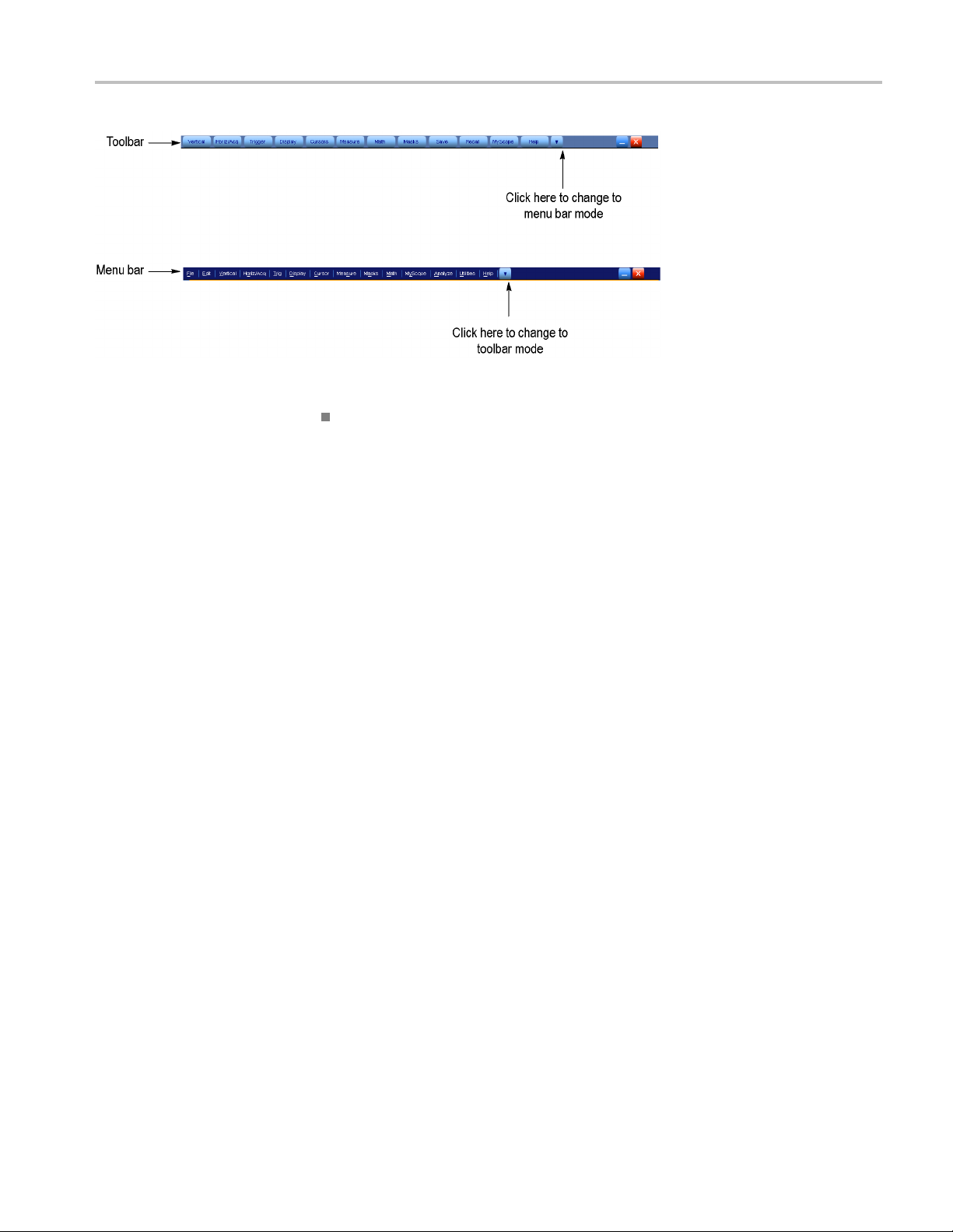
Figure 2-1: Toolbar and menu bar (< 4 GHz models shown)
The procedures assume you have connected a mouse to the instrument so you
can click on the screen controls. If you have not connected a mouse, you can
use the touch screen to operate the screen controls.
Performance Verification
MSO70000, DSA/DPO70000/B, DPO7000 Series Specifications and Performance Verification 2–3

Brief Procedures
Brief Procedu
Self Tests
res
The Self Test
adjustment. No test equipment is required to do these test procedures.
The Functio
test-signal source for further verifying that the instrument functions properly. A
BNC cable and an adaptor or a probe, depending on your instrument model are
required to do these test procedures.
This procedure uses internal routines to verify that the instrument functions and
was adjusted properly. No test equipment or hookups are required.
Equipme
None Power on the instrument and allow a
s use internal routines to confirm basic functionality and proper
nal Tests utilize the probe-compensation output at the front panel as a
nt required
Prerequ
20 minut
procedure.
isites
e warm-up before doing this
2–4 MSO70000, DSA/DPO70000/B, DPO7000 Series Specifications and Performance Verification

Brief Procedures
1. Verify that int
passing of internal diagnostics.
a. Display the S
If the instrument is in toolbar mode, put the instrument into menu bar
mode.
Pull down the Utilities menu and select Instrument Diagnostics. . . .
This dis
b. Run the System Diagnostics:
c. Wait: The internal diagnostics do an exhaustive verification of proper
instrument function. This verifi cation may take several minutes. When the
verification is finished, the resulting status will appear in the diagnostics
control window.
d. Verify that no failures are found and reported on-screen. All tests should
pass.
e. Run the signal-path compensation routine:
ernal diagnostics pass: Do the following substeps to verify
ystem diagnostics menu:
plays the diagnostics control window.
First disconnect any input signals from all four channels.
Click the Run button in the diagnostics control window.
Functional Tests
Pull down the Utilities menu and select Instrument Calibration. . . .
This displays the instrument calibration control window.
If required because the instrument is in service mode, select the Signal
Path button under Calibration Area.
Click the Run SPC (Calibrate on some instruments) button to start the
routine.
f. Wait: Signal-path compensation may take five to fifteen minutes to run.
g. Confirm signal-path compensation returns passed status: Verify that the
word Pass appears in the instrument calibration control window.
2. Return to regular service: Click the X (close) button to exit the instrument
calibration control window.
The purpose of these procedures is to confirm that the instrument functions
properly. The only equipment required is a BNC or SMA cable and an adapter or
the instrument probe. If you need to store settings during these procedures, access
the local C: drive and store them in the TekScope > Setups directory.
STOP. These procedures verify functions; that is, they verify that the instrument
features operate. They do not verify that they operate within limits.
MSO70000, DSA/DPO70000/B, DPO7000 Series Specifications and Performance Verification 2–5
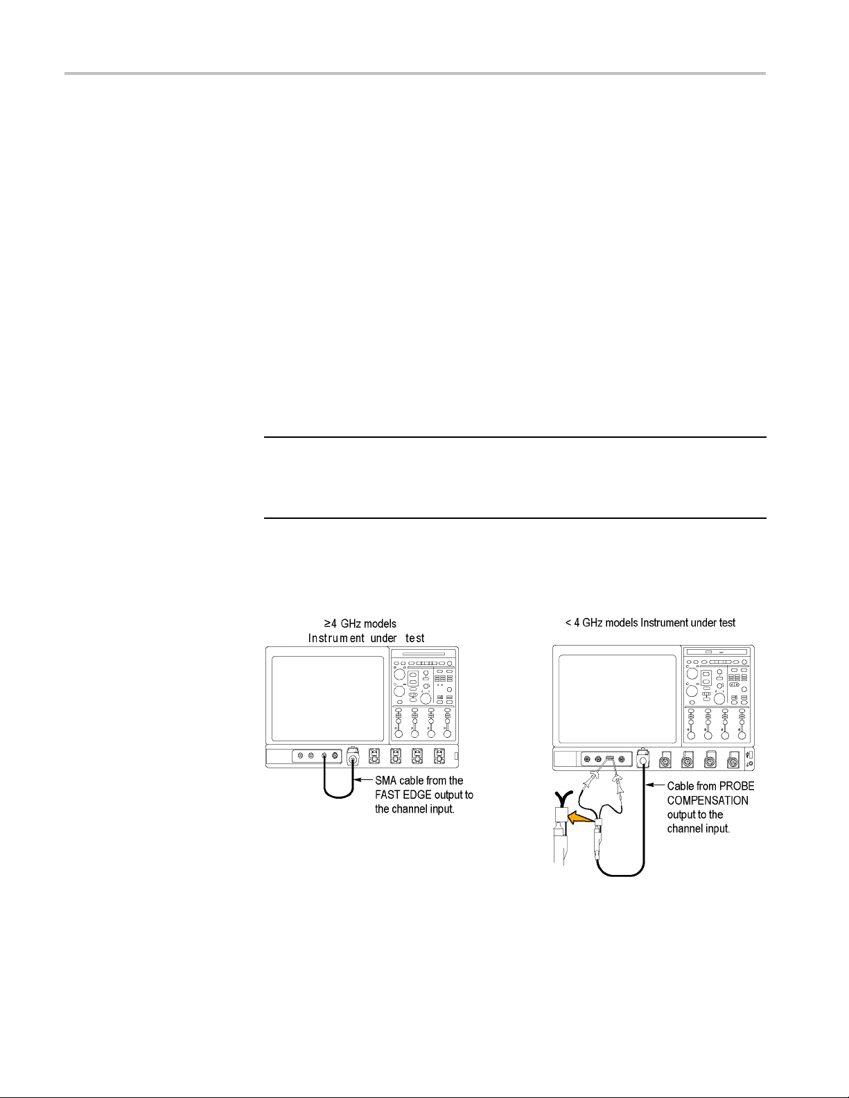
Brief Procedures
Verify All Analog Input
Channels
Therefore, whe
n the instructions in the functional tests that follow call for you to
verify that a signal appears on-screen "that is about five divisions in amplitude"
or "has a period of about six horizontal divisions," etc., do NOT interpret the
quantities given as limits. Operation within limits is checked in Performance
Tests. (See page 2-18, Performance Tests.)
STOP. DO NOT make changes to the front-panel settings that are not called
out in the procedures. Each verification procedure will require you to set the
instrument to certain default settings before verifying functions. If you make
changes to
these settings, other than those called out in the procedure, you may
obtain invalid results. In this case, just redo the procedure from step 1.
When you a
re instructed to press a front-panel or screen button, the button may
already be selected (its label will be highlighted). If this is the case, it is not
necessary to press the button.
Equipment required Prerequisites
< 4 GHz models: One precision 50 Ω coaxial cable (Item 4)
< 4 GHz models: One BNC to Minigrabber adapter (item 18)
≥ 4 GHz models: One SMA cable (item 21)
≥ 4 GHz models: One adapter (item 19)
None
1. Initi
alize the instrument: Push the front-panel Default Setup button.
2. Hook up the signal source: Connect the equipment as shown in the following
figure to the channel input you want to test (beginning with Ch 1).
Figure 2-2: Universal test hookup for functional tests - Ch 1 shown
2–6 MSO70000, DSA/DPO70000/B, DPO7000 Series Specifications and Performance Verification
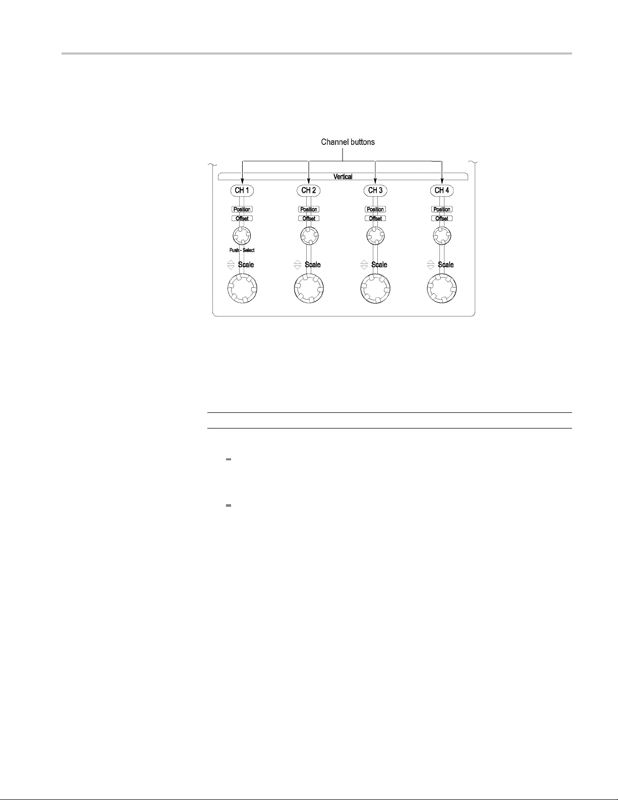
Brief Procedures
3. Turn off all cha
push those buttons to turn off the displayed channels as shown in the
following figure.
Figure 2-3: Channel button location
4. Select the channel to test: Push the channel button for the channel you are
currently testing. The button lights and the channel display comes on.
nnels: If any of the front-panel channel buttons are lighted,
5. Set up the instrument:
NOTE. If the AutoSet Undo window appears, click the X.
Push the front panel Autoset button. This sets the horizontal and vertical
scale and vertical offset for a usable display and sets the trigger source to
hannel you are testing.
the c
Pull down the Vert i ca l menu, select Vertical Setup. Confirm that the Ch1
set is about 0.0 mV.
Off
MSO70000, DSA/DPO70000/B, DPO7000 Series Specifications and Performance Verification 2–7

Brief Procedures
6. Verify that the
channel is operational: Confirm that the following statements
are true.
Verify that th
e vertical scale readout and the waveform amplitude for the
channel under test. (See Table 2-1.)
Table 2-1: Vertical settings
<4GHzmodels ≥ 4 GHz models
Setting Without probe Without probe
Scale
Waveform amplitude
500 mV 100 mV
2 division
s
4 division
s
The front-panel vertical Position knob (for the channel you are testing)
moves the signal up and down the screen when rotated.
Turning the vertical Scale knob counterclockwise (for the channel
you are testing) decreases the a mplitude of the waveform on-screen,
turning the knob clockwise increases the amplitude, and returning the
knob to
the original s cale setting returns the original amplitude for
that scale setting. (See Table 2-1.)
7. Verif
y that the channel acquires in all acquisition modes: Pull down the
Horiz/Acq menu to select Horizontal/Acquisition Setup. . . . Click the
2–8 MSO70000, DSA/DPO70000/B, DPO7000 Series Specifications and Performance Verification

Brief Procedures
Acquisition ta
b in the control window that displays. Click each of the
acquisition modes and confirm that the following statements are true.
Sample mode di
splays an actively acquiring waveform on-screen. (Note
that there is a small amount of noise present on the square wave).
Peak Detect
mode displays an actively acquiring waveform on-screen with
the noise present in Sample mode "peak detected".
HiResmoded
isplays an actively acquiring waveform on-screen with the
noise that was present in Sample mode reduced.
Average mo
de displays an actively acquiring waveform on-screen with
the noise reduced.
Envelope
mode displays an actively acquiring waveform on-screen with
the noise displayed.
NOTE. Default setup enables enhanced triggering. Enhanced triggering can
cause a slower acquisition rate that can be noticed in waveform database mode.
As waveform database mode acquires 100,000 samples, the display intensity
will increase, be cleared, and then the process will s t art over. When enhanced
ering is turned off, and with the specified settings and input signal, the
trigg
display reaches full intensity right away.
Verify the Time Base
form Database mode displays an actively acquiring waveform
Wave
on-screen with the noise displayed.
8. Te s
t all channels: Repeat steps 2 through 7 until all four input channels are
verified.
move the test hookup: Disconnect the equipment from the instrument.
9. Re
Equipment required Prerequisites
< 4 GHz models: One precision 50 Ω coaxial
cable (Item 4)
< 4 GHz models: One BNC to Minigrabber
adapter (item 18)
≥ 4 GHz models: One SMA cable (item 21)
≥ 4 GHz models: One adapter (item 19)
None
1. Initialize the instrument: Push the front-panel Default Setup button.
2. Hook up the signal source: Connect the probe compensation or fast edge
output to the Ch 1 input as shown in the following figure.
MSO70000, DSA/DPO70000/B, DPO7000 Series Specifications and Performance Verification 2–9

Brief Procedures
Figure 2-4: Setup for time base test
3. Set up the instrument: Push the front panel Autoset button.
4. Set the Ve rt ic al Sc al e to 200 mV per division.
5. Set the time base: Set the horizontal Scale to 200 μs/div.Thetime-base
readout is displayed at the bottom of the graticule.
6. Verify that the time base operates: Confirm the following statements.
One period of the square-wave signal is about five horizontal divisions
on-screen for the 200 μs/div horizontal scale setting.
Rotating the horizontal Scale knob clockwise expands the waveform
on-screen (more horizontal divisions per waveform period),
counterclockwise rotation contracts it, and returning the horizontal scale
to 200 μs/divreturnstheperiodtoaboutfive divisions.
The horizontal Position knob positions the signal left and right on-screen
when rotated.
2–10 MSO70000, DSA/DPO70000/B, DPO7000 Series Specifications and Performance Verification

Brief Procedures
7. Verify horizon
a. Center a rising edge on screen:
b. Turn on and set horizontal delay:
c. Verify the waveform: Verify that a rising edge of the waveform is within a
few divisions of center screen.
tal delay:
Set the horizontal Position knob so that the rising edge where the
waveform is triggered is lined up with the center horizontal graticule.
Change the horizontal Scale to 20 μs/div. The rising edge of the
waveform should remain near the center graticule and the falling edge
should be of
Pull down the Horiz/Acq menu to select Horizontal/Acquisition
Setup. . . .
Click the Horizontal tab in the control window that displays.
Click the Delay Mode buttontoturndelayon.
Double click the Horiz Delay control in the control window to display
the pop-up keypad. Click the keypad buttons to set the horizontal
delay to 1msandthenclicktheENTER key.
fscreen.
d. Adjust the horizontal delay: Rotate the upper multipurpose knob to change
the horizontal delay setting. Verify that the rising edge shifts horizontally.
Rotate the front-panel horizontal Position knob. Verify that this knob has
same effect (it also adjusts delay, but only when delay mode is on).
the
e. Verify the delay toggle function:
Rotate the front-panel horizontal Position knob to center the rising
edge horizontally on the screen.
Change the horizontal Scale to 50 ns/div (< 4 GHz models) or
40 ns/div (≥ 4 GHz models). The rising edge of the waveform should
emain near the center graticule.
r
Readjust the delay setting to position the rising edge 2 divisions to the
right of the center graticule line.
Push the front-panel Delay button several times to toggle delay off
and on and back off again. Verify that the display switches quickly
between two different points in time (the rising edge shifts horizontally
on the display).
8. Remove the test hookup: Disconnect the test hookup from the instrument.
MSO70000, DSA/DPO70000/B, DPO7000 Series Specifications and Performance Verification 2–11

Brief Procedures
VerifytheA(M
ain) and B
(Delayed) Trigger Systems
Equipment required Prerequisites
< 4 GHz models: One precision 50 Ω coaxial
cable (Item 4)
< 4 GHz models:
adapter (item 18)
≥ 4 GHz models: One SMA cable (item 21)
≥ 4 GHz models
One BNC to Minigrabber
: One adapter (item 19)
None
1. Initialize the instrument: Push the front-panel Default Setup button.
2. Hook up the signal source: Connect the probe compensation or fast edge
output to the Ch 1 input as shown in the following figure.
Figure 2-5: Setup for trigger test
3. Set up the instrument: Push the front-panel Autoset button.
4. Set the Ve rt ic al Sc al e to 200 mV per division.
5. Verify that the main trigger system operates: Confirm that the following
statements are true.
The trigger level readout for the A (main) trigger system changes with the
trigger-Level knob.
The trigger-Level knob can trigger and untrigger the square-wave signal
as you rotate the knob. (Leave the signal untriggered).
Pushing the front-panel trigger Level knob sets the trigger level to the
50% amplitude point of the signal and triggers the signal that you just left
untriggered. (Leave the signal triggered.)
2–12 MSO70000, DSA/DPO70000/B, DPO7000 Series Specifications and Performance Verification

Brief Procedures
6. Verify that the
delayed trigger system operates:
a. Set up the delayed trigger:
Pull down the Trig menu and select A – B Trigger Sequence. . . .This
displays the A →B Sequence tab of the trigger setup control window.
Click the Trig After Time button under A Then B.
Click the B Trig Level control in the control window.
Set the front-panel trigger mode to Norm.
b. Confirm that the following statements are true:
The trigg
er-level readout for the B trigger system changes as you turn
the lower multipurpose knob.
As you ro
tate the lower multipurpose knob, the square-wave signal
can become triggered and untriggered. (Leave the signal triggered.)
c. Verify
the delayed trigger counter:
Double click the Trig Delay control to pop up a numeric keypad for
ontrol.
that c
Click the keypad to enter a trigger delay time of 1 second (click 1
and No
ne) and then click Enter.
rifytheFileSystem
Ve
Verify that the trigger Ready indicator on the front panel flashes about
every second as the waveform is updated on-screen.
once
7. Remove the test hookup: Disconnect the test hookup from the instrument.
Equipment required Prerequisites
e
< 4 GHz models: One precision 50 Ω coaxial
cable (Item 4)
GHz models: O ne BNC to Minigrabber
<4
adapter (item 18)
≥ 4 GHz models: One SMA cable (item 21)
4 GHz models: One adapter (item 19)
≥
Non
1. Initialize the instrument: Push the front-panel Default Setup button.
2. Hook up the signal source: Connect the probe compensation or fast edge
output to the Ch 1 input as shown in the following.
MSO70000, DSA/DPO70000/B, DPO7000 Series Specifications and Performance Verification 2–13

Brief Procedures
Figure 2-6: Setup for the file system test
3. Set up the instrument: Push the front panel Autoset button.
4. Set the Ve
5. Set the time base: Set the horizontal Scale to 1ms/div. The time-base readout
is displ
6. Save the settings:
a. Pull down the File menu to select SaveAs...>Setup.... This displays
b. Note the default location and filenameandthenclicktheSave button to
7. Change the settings again: Set the horizontal SCALE to 200 μs/div.
8. Verify the file system works:
a. Pull down the File menu to select Recall. This displays the instrument
b. Click Recall What > Setup.
c. Locate and then double click the setup file that you previously stored.
d.V
rtical Scale to 200 mV per division.
ayed at the bottom of the graticule.
the instrument Save As control window.
save the setup to the default file name and location.
Recall control window.
erify t hat the instrument retrieved the saved setup. Do this by noticing
the horizontal SCALE is again 1 ms and the waveform shows ten cycles
just as it did when you saved the setup.
9. Remove the test hookup: Disconnect the test hookup from the instrument.
2–14 MSO70000, DSA/DPO70000/B, DPO7000 Series Specifications and Performance Verification

Brief Procedures
Verify the Dig
ital Channels
(MSO70000 Series Only)
Equipment required Prerequisites
MSO70000 models: One precision 50 Ω coaxial
cable (item 4)
MSO70000 mode
MSO70000 models: One SMA adapter (item 17)
MSO70000 models: One logic probe (item 31)
ls: One probe tip adapter (item 30)
None
1. Hook up the signal source: Connect the probe compensation or fast edge
output to th
e D0 input as shown in the following fi gure.
Figure 2-7: Setup for the digital channels test
2. Set up the instrument: Push the front panel Default Setup button.
3. Set the Horizontal Scale to 1ms/div.
4. Initialize the instrument: Pull down the Digital menu and select Digital
Setup. This displays the instrument Digital Setup control window.
MSO70000, DSA/DPO70000/B, DPO7000 Series Specifications and Performance Verification 2–15
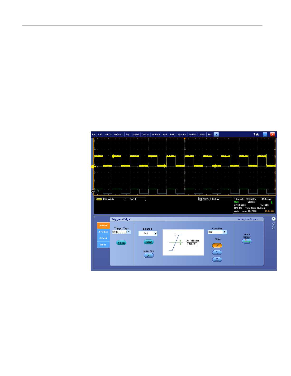
Brief Procedures
5. Press the D0 but
6. Double click Global Threshold. Use the keypad to enter 200 mV.
Press the Apply button.
7. Pull down the Ver t i c a l menu and select Ve rt i ca l Se tu p.
8. Press Digital input iCapture.
9. From the Digital Source list select D0.
10. Pull down t
11. From the Source list select D0.
12. Verify that the both the iCapture and the digital channel are triggered.
ton.
he Tr ig menu and select A Event (Main) Trigger Setup.
13. Rotate the Vertical SCALE knob counter clockwise.
14. Verify that the displayed amplitude of channel 1 is reduced.
15. Rotate the Vertical SCALE knob clockwise, back to its original setting.
16. Verify that the displayed amplitude of channel 1 returns to about 1.75
divisions (420 mV).
17. Rotate the Vertical Position knob counter clockwise.
2–16 MSO70000, DSA/DPO70000/B, DPO7000 Series Specifications and Performance Verification

Brief Procedures
18. Verify that the
19. Rotate the Vertical Position knob clockwise, back to its original setting.
20. Pull down the Digital menu and select Digital Setup.
21. Double click the D0 Position and enter -1.66 and press Enter.
22. Verify that the displayed position of digital channel moves up on the display.
23. Repeat steps 1 through 22, replacing D0 with the digital channel number of
the next channel you want to verify.
24. Remove the test hookup: Disconnect the test hookup from the instrument.
displayed position of channel 1 moves lower on the display.
MSO70000, DSA/DPO70000/B, DPO7000 Series Specifications and Performance Verification 2–17

Performance Tests
Performance T
Prerequisites
ests
This section
instrument performs as warranted.
The procedures are arranged in logical groupings: Signal Acquisition System
Checks, Time Base System Checks, Triggering System Checks, Output Ports
Checks, and Serial Trigger C hecks. They check all the characteristics that are
designated as checked in Specifications. (The characteristics that are checked
appear with a
STOP. These procedures extend the confidence level provided by the basic
procedures. The basic procedures should be done first, then these procedures
performed if desired.
The tests in this section comprise an extensive, valid confirmation of performance
and functionality when the following requirements are met:
The cabinet must be installed on the instrument.
You must have performed and passed the procedures under Self Tests,,and
those under Functional Tests. (See page 2-5, Functional Tests.)
contains a collection of manual procedures for checking that the
in Specifications).
Equipment Required
A signal-path compensation must have been done within the recommended
calibration interval and at a temperature within ±5 ºC (±9 ºF) of the present
operating temperature. (If at the time you did the prerequisite Self Tests, the
temperature was within the limits just stated, consider this prerequisite met).
A signal-path compensation must have b een done at an ambient humidity
within 25% of the current ambient humidity and after having been at that
humidity for at least 4 hours.
The instrument must have been last adjusted at an ambient temperature
between +18 ºC (+64 ºF) and +28 ºC (+82 ºF), must have been operating for a
warm-upperiodofatleast20minutes,andmustbeoperatingatanambient
temperature as listed in the specifications. (See Table 1-10 on page 1-46.)
(The warm-up requirement is usually met in the course of meeting the Self
Tests and Functional Tests prerequisites listed above).
Support sensor, probe, and adapter setups to avoid stress or torque when
connected to the device under test (DUT).
Procedures starting on (See page 2 -49.), use external, traceable signal s ources to
directly check warranted characteristics. The following table lists the required
equipment.
2–18 MSO70000, DSA/DPO70000/B, DPO7000 Series Specifications and Performance Verification

Performance Tests
Table 2-2: Test
1. Attenuator, 1
equipment
0X (two
required)
2. Attenuator, 5X
3. Terminati
on, 50 Ω (three
required)
4. Cable, Precision 50 Ω
Coaxial (
three required)
5. Connector, Dual-Banana
quired)
(two re
6. Genera
tor, DC
Calibration
7. Gene
8. Time
rator, Calibration
r-counter
9. Generator, Sine-Wave
Minimum requi
Ratio: 10X; im
rements
pedance 50 Ω;
connectors: female input,
male output
Ratio: 5X; i
mpedance 50 Ω;
connectors: female input,
male output
Impedance
50 Ω; connectors:
female BNC input, male BNC
output
50 Ω, 36 in, male-to-male
BNC conne
ctors
Female BNC-to-dual banana
Variable amplitude to ±7 V;
acy to 0.1%
accur
500 mV square wave
brator amplitude; accuracy
cali
to 0.25%
z and 100 MHz, 1 s
10 MH
gate
Instrument bandwidth ≤3GHz:
z to at least the instrument
5kH
bandwidth. Variable amplitude
from 60 mV to 2 V
requency error <2.0%
.F
strument bandwidth >3 GHz:
In
into 50 Ω
p-p
50 MHz to at least the
instrument bandwidth.
ariable amplitude from
V
60 mV to 2.0 V
into 50 Ω.
p-p
Frequency error <2.0%
Example Purpose
BNC ≤ 2GHzTekt
number 011-0059-03
ronix part
Signal attenu
bandwidth, trigger sensitivity
SMA ≤ 18 GHz Tektronix part
number 015-1
BNC ≤ 2GHzTe
number 011-0060-02
003-00
ktronix part
Signal atte
bandwidth, trigger sensitivity
SMA ≤ 18 GHz Tektronix part
number 015-
Tektronix part number
011-0049-
Tektronix part number
012-0482-00
1002-01
02 (1 GHz)
Signal ter
delay test, trigger sensitivity
Signal interconnection,
Trigger o
trigger, timebase delay time,
baud rate limit, bandwidth,
input re
clock recovery, generator
leveling
Tektronix part number
103-0090-00
Fluke 9500B
1
Various accuracy tests, input
resistance
Checki
measurement accuracy,
probe compensation out, and
um input voltage
maxim
Fluke 9500B
1
eck accuracy of signal
To c h
out, trigger out
ntest R5360
Adva
Checking long-term sample
rate and delay time accuracy
Fluke 9500B
1
Checking analog bandwidth,
gger sensitivity,
tri
sample-rate, external clock,
trigger sensitivity, time
alified trigger, baud rate
qu
ritsu MG3692B or
An
MG3694B Synthesized
limit, clock recovery, and
delay-time accuracy
CW Generator with options
x (step attenuator), 3 (low
2
noise >2 GHz), 4 (10 MHz to
2 GHz low phase noise), 15
high power), and 16 (high
(
stability)
ation,
nuation,
mination for channel
ut, time qualified
sistance, delta time,
ng DC offset, gain,
MSO70000, DSA/DPO70000/B, DPO7000 Series Specifications and Performance Verification 2–19

Performance Tests
ements
ent bandwidth.
p-p
nge: DC to
10. Meter, Level and Power
Sensor
11. Splitter, Power
Minimum requir
Frequency range: 50 MHz
to the instrum
Amplitude range: 6 mV
2V
p-p
Instrument bandwidth ≤3GHz:
Frequency ra
18 GHz. Tracking: <2.0%
Instrument bandwidth >3 GHz:
Frequency range: DC to
40 GHz. Trac
12. Cable 2.92 mm mal
13. Adapter
Kmale-to-maleDCto40GHz
king: <2.0%
e-to-female
14. Adapter (four required) Male N-to-female BNC
15. Adapter
Female N-to-male BNC
16. Adapter (three required) SMA female-to-female
17. Adapter (three required) SMA male-to-female BNC
18. Adapter
19. Adap
ter (four required)
20. Pulse Generator
BNC to Minigrabber
ale-to-BNC female
SMA m
MHz, ≤ 150 ps rise time,
250
5 V out
21. Cable, Coaxial (three
required)
22. Adapter
50 Ω, 20 in, male-to-male
SMA connectors
MA "T", male to 2 SMA
S
female
dapter
23.A
24. Adapter
SMA female to BNC male
BNC male to female elbow
Example Purpose
Rohde & Schwar
NRV-Z15 (40 GHz)
z NRVS and
Checking anal
and Trigger Sensitivity
og bandwidth
to
Agilent part number 11667A
Checking trigger sensitivity
and analog ba
ndwidth
Anritsu K241C (40 GHz)
Gore Phase
Flex cable
Checking a
nalog bandwidth
EL0CQ0CP0360 (40 GHz)
Anritsu K
Tektroni
220B
x part number
Checking analog bandwidth
Checking analog bandwidth
103-0045-00
ix part number
Tekt r on
Checking analog bandwidth
103-0058-00 (4 GHz)
ix part number
Tekt r on
Checking trigger sensitivity
015-1012-00 (18 GHz)
nix part number
Tekt r o
015-1018-00
Tektronix part number
013-0342-xx
BNC or TCA-292mm
TCAand, if required, SMA
male-to-BNC female adapter
tronix part number
(Tek
015-0554-00 (4 GHz) or
015-1018-00)
Checking the delay between
channels, delta time
Checking probe
nsation output
compe
al interconnection,
Sign
measurement accuracy,
delay time, time qualified
ger, trigger sensitivity,
trig
DC gain, offset, bandwidth,
input resistance, probe
pensation out, baud rate
com
limit, clock recovery
ke 9500B
Flu
1,2
d to test delta time
Use
measurement accuracy
ktronix part number
Te
174-1427-00
ed to test delta time
Us
measurement accuracy,
probe compensation out,
igger sensitivity
tr
Tektronix part number
15-1016-00 (18 GHz)
0
ektronix part number
T
015-0572-00 (4 GHz)
Used to test delta time
easurement accuracy
m
sed to test delta time
U
measurement accuracy and
trigger sensitivity
Tektronix part number
103-0031-00
Used to test delta time
measurement accuracy
2–20 MSO70000, DSA/DPO70000/B, DPO7000 Series Specifications and Performance Verification

Performance Tests
Minimum requir
25. Termination
26. Attenuator, 2
27. Digital Multimeter
28. Cable, coaxial 50 Ω, 39.37 in (1.0 m),
29. Mouse or keyboard Tektronix part numbers:
30. Probe ti
31. Logic probe P6717 or P6780 Logic Probe Tektronix part P6717 or
1
Fluke 9500B/1100, 9500B/3200, or 9500B/2200 and an output head (9510 or 9530) appropriate for the bandwidth of the instrument being tested.
2
For Delta Time Measurement Accuracy, use a Fluke 9500B or a pulse generator with the specified rise time. (See Table 2-11 on page 2-91.)
X
p adapter
Short circuit
female
Ratio: 2X; impedance 50 Ω;
connectors: female BNC
input, male B
Ohms: <60 Ohms
male-to-m
50 Ω,60in(1.5m),
male-to-male SMA connectors
BNC female to square pin
adapter, 50 Ω
ements
, SMA connector,
NC output
ale SMA connectors
Example Purpose
Tektronix part number
015-1021-00 (
Tektronix par
011-0069-02 (2 GHz)
Keithley 2700
Tektronix part number
174-1341-00
Tektronix
174-1428-00
119-6298
119-6297-xx (keyboard)
Tekt r on
067–1734–00
P6780
18 GHz)
t number
part number
-xx (mouse)
ix part number
Used to test delta time
measurement a
Used to test de
measurement accuracy,
pulse trigger accuracy, time
qualified tri
sensitivity, and channel
isolation
Checking input impedance
Checking analog bandwidth
and delta t
accuracy. Checking ≥ 4GHz
models serial trigger baud
rate limi
Used to input test selections
Checking digital channels
Checking digital channels
gger, trigger
ime measurement
ts
ccuracy
lta time
MSO70000 Series, DSA/DPO70000/B, and DPO7000 Series Test Record
Photocopy this table and use it to record the performance test results for your
instrument.
MSO70000, DSA/DPO70000/B, DPO7000 Series Specifications and Performance Verification 2–21

Performance Tests
Table 2-3: MSO7
Instrument Serial Number:
Temperature:
Date of Calibr
Instrument pe
DC voltage me
and MSO70000 Series
Ch1 10 mV Vert scale setting,
-5 Div position setting, +0.45 V offset
Ch1 10 mV Vert scale setting,
+5 Div posi
Ch1 20 mV Ve
-5 Div position setting, +0.4 V offset
Ch1 20 mV Vert scale setting,
+5 Div position setting, -0.4 V offset
Ch1 50 mV Vert scale setting,
-5 Div po
Ch1 50 m
Ch1 100 mV Vert scale setting,
Ch1 100 mV Vert scale setting,
Ch1 2
Ch1 250 mV Vert scale setting,
Ch1 500 mV Vert scale setting,
Ch
Ch2 10 mV Vert scale setting,
Ch2 10 mV Vert scale setting,
Ch2 20 mV Vert scale setting,
Ch2 20 mV Vert scale setting,
Ch2 50 mV Vert scale setting,
Ch2 50 mV Vert scale setting,
V Vert scale setting,
+5 Div position setting, -0.25 V offset
-5 Div position setting, +2.0 V offset
v position setting, -2.0 V offset
+5 Di
50 mV Vert scale setting,
-5 Div position setting, +1.25 V offset
+5 Div position setting, -1.25 V offset
Div position setting, 0V offset
-5
1 500 mV Vert scale setting,
+5 Div position setting, -0 V offset
-5 Div position setting, +0.45 V offset
+5 Div position setting, -0.45 V offset
-5 Div position setting, +0.4 V offset
+5 Div position setting, -0.4 V offset
-5 Div position setting, +0.25 V offset
+5 Div position setting, -0.25 V offset
0000, DPO/DSA70000B, DPO/DSA70000, DPO7000 Series Test Record
ation:
rformance test
asurement accuracy (averaged), ≥ 4GHzBmodels
tion setting, -0.45 V offset
rt scale setting,
sition setting, +0.25 V offset
Certificate Number:
RH %:
Technician:
Minimum Incoming Outgoing Maximum
+ 524.75 mV
- 535.25 mV
+ 552.75 mV
- 567.25 m
+ 636.75 mV
- 663.25 mV
+ 2.696
- 2.904 V
+ 2.994 V
-3.
+ 3.326 V
- 3.674 V
+
- 535.25 mV
+ 552.75 mV
- 567.25 mV
+ 636.75 mV
- 663.25 mV
V
256 V
524.75 mV
V
__________ __________
__________ __________
__________ __________
________
__________ __________
__________ __________
_____
__________ __________
__________ __________
___
__________ __________
__________ __________
_________
_
__________ __________
__________ __________
__________ __________
__________ __________
__________ __________
__
_____
_______
________
_____
___
_________
_
__
_____
_______
+535.25mV
- 524.75 mV
+567.25mV
- 552.75 m
+663.25mV
- 636.75 mV
+2.904
-2.696V
+3.256V
994 V
-2.
+3.674V
-3.326V
535.25 mV
+
- 524.75 mV
+567.25mV
- 552.75 mV
+663.25mV
- 636.75 mV
V
V
2–22 MSO70000, DSA/DPO70000/B, DPO7000 Series Specifications and Performance Verification

Performance Tests
Table 2-3: MSO70000, DPO/DSA70000B, DPO/DSA70000, DPO7000 Series Test Record (cont.)
Instrument performance test Minimum Incoming Outgoing Maximum
Ch2 100 mV Vert scale s etting,
-5 Div position setting, +2.0 V offset
Ch2 100 mV Vert scale s etting,
+5 Div position setting, -2.0 V offset
Ch2 250 mV Vert scale s etting,
-5 Div position setting, +1.25 V offset
Ch2 250 mV Vert scale s etting,
+5 Div position setting, -1.25 V offset
Ch2 500 mV Vert scale s etting,
-5 Div position setting, 0V offset
Ch2 500 mV Vert scale s etting,
+5 Div position setting, -0 V offset
Ch3 10 mV Vert scale setting,
-5 Div position setting, +0.45 V offset
Ch3 10 mV Vert scale setting,
+5 Div position setting, -0.45 V offset
Ch3 20 mV Vert scale setting,
-5 Div position setting, +0.4 V offset
Ch3 20 mV Vert scale setting,
+5 Div position setting, -0.4 V offset
Ch3 50 mV Vert scale setting,
-5 Div position setting, +0.25 V offset
Ch3 50 mV Vert scale setting,
+5 Div position setting, -0.25 V offset
Ch3 100 mV Vert scale s etting,
-5 Div position setting, +2.0 V offset
Ch3 100 mV Vert scale s etting,
+5 Div position setting, -2.0 V offset
Ch3 250 mV Vert scale s etting,
-5 Div position setting, +1.25 V offset
Ch3 250 mV Vert scale s etting,
+5 Div position setting, -1.25 V offset
Ch3 500 mV Vert scale s etting,
-5 Div position setting, 0V offset
Ch3 500 mV Vert scale s etting,
+5 Div position setting, -0 V offset
Ch4 10 mV Vert scale setting,
-5 Div position setting, +0.45 V offset
Ch4 10 mV Vert scale setting,
+5 Div position setting, -0.45 V offset
Ch4 20 mV Vert scale setting,
-5 Div position setting, +0.4 V offset
+ 2.696 V
- 2.904 V
+ 2.994 V
- 3.256 V
+ 3.326 V
- 3.674 V
+ 524.75 mV
- 535.25 mV
+ 552.75 mV
- 567.25 mV
+ 636.75 mV
- 663.25 mV
+ 2.696 V
- 2.904 V
+ 2.994 V
- 3.256 V
+ 3.326 V
- 3.674 V
+ 524.75 mV
- 535.25 mV
+ 552.75 mV
__________ __________
__________ __________
__________ __________
__________ __________
__________ __________
__________ __________
__________ __________
__________ __________
__________ __________
__________ __________
__________ __________
__________ __________
__________ __________
__________ __________
__________ __________
__________ __________
__________ __________
__________ __________
__________ __________
__________ __________
__________ __________
+ 2.904 V
- 2.696 V
+ 3.256 V
- 2.994 V
+ 3.674 V
- 3.326 V
+ 535.25 mV
- 524.75 mV
+ 567.25 mV
- 552.75 mV
+ 663.25 mV
- 636.75 mV
+ 2.904 V
- 2.696 V
+ 3.256 V
- 2.994 V
+ 3.674 V
- 3.326 V
+ 535.25 mV
- 524.75 mV
+ 567.25 mV
MSO70000, DSA/DPO70000/B, DPO7000 Series Specifications and Performance Verification 2–23

Performance Tests
Table 2-3: MSO70000, DPO/DSA70000B, DPO/DSA70000, DPO7000 Series Test Record (cont.)
Instrument performance test Minimum Incoming Outgoing Maximum
Ch4 20 mV Vert scale setting,
+5 Div position setting, -0.4 V offset
Ch4 50 mV Vert scale setting,
-5 Div position setting, +0.25 V offset
Ch4 50 mV Vert scale setting,
+5 Div position setting, -0.25 V offset
Ch4 100 mV Vert scale setting,
-5 Div position setting, +2.0 V offset
Ch4 100 mV Vert scale setting,
+5 Div position setting, -2.0 V offset
Ch4 250 mV Vert scale setting,
-5 Div position setting, +1.25 V offset
Ch4 250 mV Vert scale setting,
+5 Div position setting, -1.25 V offset
Ch4 500 mV Vert scale setting,
-5 Div position setting, 0V offset
Ch4 500 mV Vert scale setting,
+5 Div position setting, -0 V offset
DC voltage measurement accuracy (averaged), ≥ 4 GHz non-B models
Ch1 10 mV Vert scale setting,
-5 Div position setting, +0.45 V offset
Ch1 10 mV Vert scale setting,
+5 Div position setting, -0.45 V offset
Ch1 20 mV Vert scale setting,
-5 Div position setting, +0.4 V offset
Ch1 20 mV Vert scale setting,
+5 Div position setting, -0.4 V offset
Ch1 50 mV Vert scale setting,
-5 Div position setting, +0.25 V offset
Ch1 50 mV Vert scale setting,
+5 Div position setting, -0.25 V offset
Ch1 100 mV Vert scale setting,
-5 Div position setting, +4.5 V offset
Ch1 100 mV Vert scale setting,
+5 Div position setting, -4.5 V offset
Ch1 200 mV Vert scale setting,
-5 Div position setting, +4 V offset
Ch1 200 mV Vert scale setting,
+5 Div position setting, -4 V offset
Ch1 500 mV Vert scale setting,
-4 Div position setting, +2.5V offset
- 567.25 mV
+ 636.75 mV
- 663.25 mV
+ 2.696 V
- 2.904 V
+ 2.994 V
- 3.256 V
+ 3.326 V
- 3.674 V
+ 524.75 mV
- 535.25 mV
+ 552.75 mV
- 567.25 mV
+ 636.75 mV
- 663.25 mV
+ 5.248 V
- 5.353 V
+ 5.430 V
- 5.571 V
+ 5.379 V
__________ __________
__________ __________
__________ __________
__________ __________
__________ __________
__________ __________
__________ __________
__________ __________
__________ __________
__________ __________
__________ __________
__________ __________
__________ __________
__________ __________
__________ __________
__________ __________
__________ __________
__________ __________
__________ __________
__________ __________
- 552.75 mV
+663.25mV
- 636.75 mV
+2.904V
-2.696V
+3.256V
-2.994V
+3.674V
-3.326V
+535.25mV
- 524.75 mV
+567.25mV
- 552.75 mV
+663.25mV
- 636.75 mV
+5.353V
-5.248V
+5.571V
-5.430V
+5.621V
2–24 MSO70000, DSA/DPO70000/B, DPO7000 Series Specifications and Performance Verification

Performance Tests
Table 2-3: MSO70000, DPO/DSA70000B, DPO/DSA70000, DPO7000 Series Test Record (cont.)
Instrument performance test Minimum Incoming Outgoing Maximum
Ch1 500 mV Vert scale s etting,
+4 Div position setting, -2.5 V offset
Ch1 1.0 V Vert scale setting,
-5 Div position setting, +0.0 V offset
Ch1 1.0 V Vert scale setting,
+5 Div position setting, -0.0 V offset
Ch2 10 mV Vert scale setting,
-5 Div position setting, +0.45 V offset
Ch2 10 mV Vert scale setting,
+5 Div position setting, -0.45 V offset
Ch2 20 mV Vert scale setting,
-5 Div position setting, +0.4 V offset
Ch2 20 mV Vert scale setting,
+5 Div position setting, -0.4 V offset
Ch2 50 mV Vert scale setting,
-5 Div position setting, +0.25 V offset
Ch2 50 mV Vert scale setting,
+5 Div position setting, -0.25 V offset
Ch2 100 mV Vert scale s etting,
-5 Div position setting, +4.5 V offset
Ch2 100 mV Vert scale s etting,
+5 Div position setting, -4.5 V offset
Ch2 200 mV Vert scale s etting,
-5 Div position setting, +4 V offset
Ch2 200 mV Vert scale s etting,
+5 Div position setting, -4 V offset
Ch2 500 mV Vert scale s etting,
-4 Div position setting, +2.5V offset
Ch2 500 mV Vert scale s etting,
+4 Div position setting, -2.5 V offset
Ch2 1.0 V Vert scale setting,
-5 Div position setting, +0.0 V offset
Ch2 1.0 V Vert scale setting,
+5 Div position setting, -0.0 V offset
Ch3 10 mV Vert scale setting,
-5 Div position setting, +0.45 V offset
Ch3 10 mV Vert scale setting,
+5 Div position setting, -0.45 V offset
Ch3 20 mV Vert scale setting,
-5 Div position setting, +0.4 V offset
Ch3 20 mV Vert scale setting,
+5 Div position setting, -0.4 V offset
-5.621V
+ 5.318 V
- 5.683 V
+ 524.75 mV
- 535.25 mV
+ 552.75 mV
- 567.25 mV
+ 636.75 mV
- 663.25 mV
+ 5.248 V
- 5.353 V
+ 5.430 V
- 5.571 V
+ 5.379 V
-5.621V
+ 5.318 V
- 5.683 V
+ 524.75 mV
- 535.25 mV
+ 552.75 mV
- 567.25 mV
__________ __________
__________ __________
__________ __________
__________ __________
__________ __________
__________ __________
__________ __________
__________ __________
__________ __________
__________ __________
__________ __________
__________ __________
__________ __________
__________ __________
__________ __________
__________ __________
__________ __________
__________ __________
__________ __________
__________ __________
__________ __________
- 5.379 V
+ 5.683 V
- 5.318 V
+ 535.25 mV
- 524.75 mV
+ 567.25 mV
- 552.75 mV
+ 663.25 mV
- 636.75 mV
+ 5.353 V
- 5.248 V
+ 5.571 V
- 5.430 V
+5.621V
- 5.379 V
+ 5.683 V
- 5.318 V
+ 535.25 mV
- 524.75 mV
+ 567.25 mV
- 552.75 mV
MSO70000, DSA/DPO70000/B, DPO7000 Series Specifications and Performance Verification 2–25

Performance Tests
Table 2-3: MSO70000, DPO/DSA70000B, DPO/DSA70000, DPO7000 Series Test Record (cont.)
Instrument performance test Minimum Incoming Outgoing Maximum
Ch3 50 mV Vert scale setting,
-5 Div position setting, +0.25 V offset
Ch3 50 mV Vert scale setting,
+5 Div position setting, -0.25 V offset
Ch3 100 mV Vert scale setting,
-5 Div position setting, +4.5 V offset
Ch3 100 mV Vert scale setting,
+5 Div position setting, -4.5 V offset
Ch3 200 mV Vert scale setting,
-5 Div position setting, +4 V offset
Ch3 200 mV Vert scale setting,
+5 Div position setting, -4 V offset
Ch3 500 mV Vert scale setting,
-4 Div position setting, +2.5 V offset
Ch3 500 mV Vert scale setting,
+4 Div position setting, -2.5 V offset
Ch3 1.0 V Vert scale setting,
-5 Div position setting, +0.0 V offset
Ch3 1.0 V Vert scale setting,
+5 Div position setting, -0.0 V offset
Ch4 10 mV Vert scale setting,
-5 Div position setting, +0.45 V offset
Ch4 10 mV Vert scale setting,
+5 Div position setting, -0.45 V offset
Ch4 20 mV Vert scale setting,
-5 Div position setting, +0.4 V offset
Ch4 20 mV Vert scale setting,
+5 Div position setting, -0.4 V offset
Ch4 50 mV Vert scale setting,
-5 Div position setting, +0.25 V offset
Ch4 50 mV Vert scale setting,
+5 Div position setting, -0.25 V offset
Ch4 100 mV Vert scale setting,
-5 Div position setting, +4.5 V offset
Ch4 100 mV Vert scale setting,
+5 Div position setting, -4.5 V offset
Ch4 200 mV Vert scale setting,
-5 Div position setting, +4 V offset
Ch4 200 mV Vert scale setting,
+5 Div position setting, -4 V offset
Ch4 500 mV Vert scale setting,
-4 Div position setting, +2.5V offset
+ 636.75 mV
- 663.25 mV
+ 5.248 V
- 5.353 V
+ 5.430 V
- 5.571 V
+ 5.379 V
-5.621V
+ 5.318 V
- 5.683 V
+ 524.75 mV
- 535.25 mV
+ 552.75 mV
- 567.25 mV
+ 636.75 mV
- 663.25 mV
+ 5.248 V
- 5.353 V
+ 5.430 V
- 5.571 V
+ 5.379 V
__________ __________
__________ __________
__________ __________
__________ __________
__________ __________
__________ __________
__________ __________
__________ __________
__________ __________
__________ __________
__________ __________
__________ __________
__________ __________
__________ __________
__________ __________
__________ __________
__________ __________
__________ __________
__________ __________
__________ __________
__________ __________
+663.25mV
- 636.75 mV
+5.353V
-5.248V
+5.571V
-5.430V
+5.621V
-5.379V
+5.683V
-5.318V
+535.25mV
- 524.75 mV
+567.25mV
- 552.75 mV
+663.25mV
- 636.75 mV
+5.353V
-5.248V
+5.571V
-5.430V
+5.621V
2–26 MSO70000, DSA/DPO70000/B, DPO7000 Series Specifications and Performance Verification

Performance Tests
Table 2-3: MSO70000, DPO/DSA70000B, DPO/DSA70000, DPO7000 Series Test Record (cont.)
Instrument performance test Minimum Incoming Outgoing Maximum
Ch4 500 mV Vert scale s etting,
+4 Div position setting, -2.5 V offset
Ch4 1.0 V Vert scale setting,
-5 Div position setting, +0.0 V offset
Ch4 1.0 V Vert scale setting,
+5 Div position setting, -0.0 V offset
DC voltage measurement accuracy (averaged), < 4 GHz models
Ch1 1 mV Vert scale setting,
-5 Div position setting, +0.5 V offset
Ch1 1 mV Vert scale setting,
+5 Div position setting, -0.5 V offset
Ch1 2 mV Vert scale setting,
-5 Div position setting, +0.5 V offset
Ch1 2 mV Vert scale setting,
+5 Div position setting, -0.5 V offset
Ch1 5 mV Vert scale setting,
-5 Div position setting, +0.5 V offset
Ch1 5 mV Vert scale setting,
+5 Div position setting, -0.5 V offset
Ch1 10 mV Vert scale setting,
-5 Div position setting, +0.5 V offset
Ch1 10 mV Vert scale setting,
+5 Div position setting, -0.5 V offset
Ch1 20 mV Vert scale setting,
-5 Div position setting, +0.5 V offset
Ch1 20 mV Vert scale setting,
+5 Div position setting, -0.5 V offset
Ch1 50 mV Vert scale setting,
-5 Div position setting, +0.5 V offset
Ch1 50 mV Vert scale setting,
+5 Div position setting, -0.5 V offset
Ch1 90 mV Vert scale setting,
-5 Div position setting, +0.5 V offset
Ch1 90 mV Vert scale setting,
+5 Div position setting, -0.5 V offset
Ch1 100 mV Vert scale s etting,
0 Div position setting, +4.5 V offset
Ch1 100 mV Vert scale s etting,
0 Div position setting, -4.5 V offset
Ch1 200 mV Vert scale s etting,
-2 Div position setting, +4.6 V offset
-5.621V
+ 5.318 V
- 5.683 V
+ 504.25 mV
- 509.76 mV
+ 512.98 mV
- 519.03 mV
+ 536.26 mV
- 543.74 mV
+ 574.20 mV
- 585.80 mV
+ 651.65 mV
- 668.35 mV
+ 884.00 mV
- 916.00 V
+ 1.194 V
- 1.246 V
+ 4.746 V
- 4.854 V
+ 4.725 V
__________ __________
__________ __________
__________ __________
__________ __________
__________ __________
__________ __________
__________ __________
__________ __________
__________ __________
__________ __________
__________ __________
__________ __________
__________ __________
__________ __________
__________ __________
__________ __________
__________ __________
__________ __________
__________ __________
__________ __________
- 5.379 V
+ 5.683 V
- 5.318 V
+ 509.76 mV
- 504.25 mV
+ 519.03 mV
- 512.98 mV
+ 543.74 mV
- 536.26 mV
+ 585.80 mV
- 574.20 mV
+ 668.35 mV
- 651.65 mV
+ 916.00 mV
- 884.00 mV
+ 1.246 V
- 1.194 V
+ 4.854 V
- 4.746 V
+ 4.875 V
MSO70000, DSA/DPO70000/B, DPO7000 Series Specifications and Performance Verification 2–27

Performance Tests
Table 2-3: MSO70000, DPO/DSA70000B, DPO/DSA70000, DPO7000 Series Test Record (cont.)
Instrument performance test Minimum Incoming Outgoing Maximum
Ch1 200 mV Vert scale setting,
+2 Div position setting, -4.6 V offset
Ch1 500 mV Vert scale setting,
-2 Div position setting, +5.0 V offset
Ch1 500 mV Vert scale setting,
+2 Div position setting, -5.0 V offset
Ch1 1.0 V Vert scale setting,
0 Div position setting, +2.0 V offset
Ch1 1.0 V Vert scale setting,
0 Div position setting, -2.0 V offset
Ch2 1 mV Vert scale setting,
-5 Div position setting, +0.5 V offset
Ch2 1 mV Vert scale setting,
+5 Div position setting, -0.5 V offset
Ch2 2 mV Vert scale setting,
-5 Div position setting, +0.5 V offset
Ch2 2 mV Vert scale setting,
+5 Div position setting, -0.5 V offset
Ch2 5 mV Vert scale setting,
-5 Div position setting, +0.5 V offset
Ch2 5 mV Vert scale setting,
+5 Div position setting, -0.5 V offset
Ch2 10 mV Vert scale setting,
-5 Div position setting, +0.5 V offset
Ch2 10 mV Vert scale setting,
+5 Div position setting, -0.5 V offset
Ch2 20 mV Vert scale setting,
-5 Div position setting, +0.5 V offset
Ch2 20 mV Vert scale setting,
+5 Div position setting, -0.5 V offset
Ch2 50 mV Vert scale setting,
-5 Div position setting, +0.5 V offset
Ch2 50 mV Vert scale setting,
+5 Div position setting, -0.5 V offset
Ch2 90 mV Vert scale setting,
-5 Div position setting, +0.5 V offset
Ch2 90 mV Vert scale setting,
+5 Div position setting, -0.5 V offset
Ch2 100 mV Vert scale setting,
0 Div position setting, +4.5 V offset
Ch2 100 mV Vert scale setting,
0 Div position setting, -4.5 V offset
- 4.875 V
+ 4.345 V
- 4.655 V
+ 4.745 V
- 5.255 V
+ 504.25 mV
- 509.76 mV
+ 512.98 mV
- 519.03 mV
+ 536.26 mV
- 543.74 mV
+ 574.20 mV
- 585.80 mV
+ 651.65 mV
- 668.35 mV
+ 884.00 mV
- 916.00 V
+ 1.194 V
- 1.246 V
+ 4.746 V
- 4.854 V
__________ __________
__________ __________
__________ __________
__________ __________
__________ __________
__________ __________
__________ __________
__________ __________
__________ __________
__________ __________
__________ __________
__________ __________
__________ __________
__________ __________
__________ __________
__________ __________
__________ __________
__________ __________
__________ __________
__________ __________
__________ __________
-4.725V
+4.655V
-4.345V
+5.255V
-4.745V
+509.76mV
- 504.25 mV
+519.03mV
- 512.98 mV
+543.74mV
- 536.26 mV
+585.80mV
- 574.20 mV
+668.35mV
- 651.65 mV
+916.00mV
- 884.00 mV
+1.246V
-1.194V
+4.854V
-4.746V
2–28 MSO70000, DSA/DPO70000/B, DPO7000 Series Specifications and Performance Verification

Performance Tests
Table 2-3: MSO70000, DPO/DSA70000B, DPO/DSA70000, DPO7000 Series Test Record (cont.)
Instrument performance test Minimum Incoming Outgoing Maximum
Ch2 200 mV Vert scale s etting,
-2 Div position setting, +4.6 V offset
Ch2 200 mV Vert scale s etting,
+2 Div position setting, -4.6 V offset
Ch2 500 mV Vert scale s etting,
-2 Div position setting, +5.0 V offset
Ch2 500 mV Vert scale s etting,
+2 Div position setting, -5.0 V offset
Ch2 1.0 V Vert scale setting,
0 Div position setting, +2.0 V offset
Ch2 1.0 V Vert scale setting,
0 Div position setting, -2.0 V offset
Ch3 1 mV Vert scale setting,
-5 Div position setting, +0.5 V offset
Ch3 1 mV Vert scale setting,
+5 Div position setting, -0.5 V offset
Ch3 2 mV Vert scale setting,
-5 Div position setting, +0.5 V offset
Ch3 2 mV Vert scale setting,
+5 Div position setting, -0.5 V offset
Ch3 5 mV Vert scale setting,
-5 Div position setting, +0.5 V offset
Ch3 5 mV Vert scale setting,
+5 Div position setting, -0.5 V offset
Ch3 10 mV Vert scale setting,
-5 Div position setting, +0.5 V offset
Ch3 10 mV Vert scale setting,
+5 Div position setting, -0.5 V offset
Ch3 20 mV Vert scale setting,
-5 Div position setting, +0.5 V offset
Ch3 20 mV Vert scale setting,
+5 Div position setting, -0.5 V offset
Ch3 50 mV Vert scale setting,
-5 Div position setting, +0.5 V offset
Ch3 50 mV Vert scale setting,
+5 Div position setting, -0.5 V offset
Ch3 90 mV Vert scale setting,
-5 Div position setting, +0.5 V offset
Ch3 90 mV Vert scale setting,
+5 Div position setting, -0.5 V offset
Ch3 100 mV Vert scale s etting,
0 Div position setting, +4.5 V offset
+ 4.725 V
- 4.875 V
+ 4.345 V
- 4.655 V
+ 4.745 V
- 5.255 V
+ 504.25 mV
- 509.76 mV
+ 512.98 mV
- 519.03 mV
+ 536.26 mV
- 543.74 mV
+ 574.20 mV
- 585.80 mV
+ 651.65 mV
- 668.35 mV
+ 884.00 mV
- 916.00 V
+ 1.194 V
- 1.246 V
+ 4.746 V
__________ __________
__________ __________
__________ __________
__________ __________
__________ __________
__________ __________
__________ __________
__________ __________
__________ __________
__________ __________
__________ __________
__________ __________
__________ __________
__________ __________
__________ __________
__________ __________
__________ __________
__________ __________
__________ __________
__________ __________
__________ __________
+ 4.875 V
- 4.725 V
+ 4.655 V
- 4.345 V
+ 5.255 V
- 4.745 V
+ 509.76 mV
- 504.25 mV
+ 519.03 mV
- 512.98 mV
+ 543.74 mV
- 536.26 mV
+ 585.80 mV
- 574.20 mV
+ 668.35 mV
- 651.65 mV
+ 916.00 mV
- 884.00 mV
+ 1.246 V
- 1.194 V
+ 4.854 V
MSO70000, DSA/DPO70000/B, DPO7000 Series Specifications and Performance Verification 2–29

Performance Tests
Table 2-3: MSO70000, DPO/DSA70000B, DPO/DSA70000, DPO7000 Series Test Record (cont.)
Instrument performance test Minimum Incoming Outgoing Maximum
Ch3 100 mV Vert scale setting,
0 Div position setting, -4.5 V offset
Ch3 200 mV Vert scale setting,
-2 Div position setting, +4.6 V offset
Ch3 200 mV Vert scale setting,
+2 Div position setting, -4.6 V offset
Ch3 500 mV Vert scale setting,
-2 Div position setting, +5.0 V offset
Ch3 500 mV Vert scale setting,
+2 Div position setting, -5.0 V offset
Ch3 1.0 V Vert scale setting,
0 Div position setting, +2.0 V offset
Ch3 1.0 V Vert scale setting,
0 Div position setting, -2.0 V offset
Ch4 1 mV Vert scale setting,
-5 Div position setting, +0.5 V offset
Ch4 1 mV Vert scale setting,
+5 Div position setting, -0.5 V offset
Ch4 2 mV Vert scale setting,
-5 Div position setting, +0.5 V offset
Ch4 2 mV Vert scale setting,
+5 Div position setting, -0.5 V offset
Ch4 5 mV Vert scale setting,
-5 Div position setting, +0.5 V offset
Ch4 5 mV Vert scale setting,
+5 Div position setting, -0.5 V offset
Ch4 10 mV Vert scale setting,
-5 Div position setting, +0.5 V offset
Ch4 10 mV Vert scale setting,
+5 Div position setting, -0.5 V offset
Ch4 20 mV Vert scale setting,
-5 Div position setting, +0.5 V offset
Ch4 20 mV Vert scale setting,
+5 Div position setting, -0.5 V offset
Ch4 50 mV Vert scale setting,
-5 Div position setting, +0.5 V offset
Ch4 50 mV Vert scale setting,
+5 Div position setting, -0.5 V offset
Ch4 90 mV Vert scale setting,
-5 Div position setting, +0.5 V offset
Ch4 90 mV Vert scale setting,
+5 Div position setting, -0.5 V offset
- 4.854 V
+ 4.725 V
- 4.875 V
+ 4.345 V
- 4.655 V
+ 4.745 V
- 5.255 V
+ 504.25 mV
- 509.76 mV
+ 512.98 mV
- 519.03 mV
+ 536.26 mV
- 543.74 mV
+ 574.20 mV
- 585.80 mV
+ 651.65 mV
- 668.35 mV
+ 884.00 mV
- 916.00 V
+ 1.194 V
- 1.246 V
__________ __________
__________ __________
__________ __________
__________ __________
__________ __________
__________ __________
__________ __________
__________ __________
__________ __________
__________ __________
__________ __________
__________ __________
__________ __________
__________ __________
__________ __________
__________ __________
__________ __________
__________ __________
__________ __________
__________ __________
__________ __________
-4.746V
+4.875V
-4.725V
+4.655V
-4.345V
+5.255V
-4.745V
+509.76mV
- 504.25 mV
+519.03mV
- 512.98 mV
+543.74mV
- 536.26 mV
+585.80mV
- 574.20 mV
+668.35mV
- 651.65 mV
+916.00mV
- 884.00 mV
+1.246V
-1.194V
2–30 MSO70000, DSA/DPO70000/B, DPO7000 Series Specifications and Performance Verification

Performance Tests
Table 2-3: MSO70000, DPO/DSA70000B, DPO/DSA70000, DPO7000 Series Test Record (cont.)
Instrument performance test Minimum Incoming Outgoing Maximum
Ch4 100 mV Vert scale s etting,
0 Div position setting, +4.5 V offset
Ch4 100 mV Vert scale s etting,
0 Div position setting, -4.5 V offset
Ch4 200 mV Vert scale s etting,
-2 Div position setting, +4.6 V offset
Ch4 200 mV Vert scale s etting,
+2 Div position setting, -4.6 V offset
Ch4 500 mV Vert scale s etting,
-2 Div position setting, +5.0 V offset
Ch4 500 mV Vert scale s etting,
+2 Div position setting, -5.0 V offset
Ch4 1.0 V Vert scale setting,
0 Div position setting, +2.0 V offset
Ch4 1.0 V Vert scale setting,
0 Div position setting, -2.0 V offset
DC gain accuracy (averaged), ≥ 4 GHz B models and MSO70000
Series
Ch1 10 mV Vert scale setting,
0 Div position setting, 0 V offset
-5 Div position setting, +0.45 V offset
+5 Div position setting, -0.45 V offset
Ch1 20 mV Vert scale setting,
0 Div position setting, 0 V offset
-5 Div position setting, +0.4 V offset
+5 Div position setting, -0.4 V offset
Ch1 50 mV Vert scale setting,
0 Div position setting, 0 V offset
-5 Div position setting, +0.25 V offset
+5 Div position setting, -0.25 V offset
Ch1 100 mV Vert scale s etting,
0 Div position setting, 0 V offset
-5 Div position setting, +2.0 V offset
+5 Div position setting, -2.0 V offset
Ch1 250 mV Vert scale s etting,
0 Div position setting, 0 V offset
-5 Div position setting, +1.25 V offset
+5 Div position setting, -1.25 V offset
Ch1 500 mV Vert scale s etting,
0 Div position setting, 0 V offset
-5 Div position setting, 0 V offset
+5 Div position setting, 0 V offset
+ 4.746 V
- 4.854 V
+ 4.725 V
- 4.875 V
+ 4.345 V
- 4.655 V
+ 4.745 V
- 5.255 V
+ 74.48 mV
+ 74.48 mV
+ 74.48 mV
+ 148.96 mV
+ 148.96 mV
+ 148.96 mV
+ 372.40 mV
+ 372.40 mV
+ 372.40 mV
+ 744.80 mV
+ 744.80 mV
+ 744.80 mV
+ 1.862 V
+ 1.862 V
+ 1.862 V
+ 3.724 V
+ 3.724 V
+ 3.724 V
__________ __________
__________ __________
__________ __________
__________ __________
__________ __________
__________ __________
__________ __________
__________ __________
__________
__________
__________
__________
__________
__________
__________
__________
__________
__________
__________
__________
__________
__________
__________
__________
__________
__________
__________
__________
__________
__________
__________
__________
__________
__________
__________
__________
__________
__________
__________
__________
__________
__________
__________
__________
+ 4.854 V
- 4.746 V
+ 4.875 V
- 4.725 V
+ 4.655 V
- 4.345 V
+ 5.255 V
- 4.745 V
+ 77.52 mV
+ 77.52 mV
+ 77.52 mV
+ 155.04 mV
+ 155.04 mV
+ 155.04 mV
+ 387.60 mV
+ 387.60 mV
+ 387.60 mV
+ 775.20 mV
+ 775.20 mV
+ 775.20 mV
+ 1.938 V
+ 1.938 V
+ 1.938 V
+ 3.876 V
+ 3.876 V
+ 3.876 V
MSO70000, DSA/DPO70000/B, DPO7000 Series Specifications and Performance Verification 2–31

Performance Tests
Table 2-3: MSO70000, DPO/DSA70000B, DPO/DSA70000, DPO7000 Series Test Record (cont.)
Instrument performance test Minimum Incoming Outgoing Maximum
Ch2 10 mV Vert scale setting,
0 Div position s etting, 0 V offset
-5 Div position setting, +0.45 V offset
+5 Div position setting, -0.45 V offset
Ch2 20 mV Vert scale setting,
0 Div position s etting, 0 V offset
-5 Div position setting, +0.4 V offset
+5 Div position setting, -0.4 V offset
Ch2 50 mV Vert scale setting,
0 Div position s etting, 0 V offset
-5 Div position setting, +0.25 V offset
+5 Div position setting, -0.25 V offset
Ch2 100 mV Vert scale setting,
0 Div position s etting, 0 V offset
-5 Div position setting, +2.0 V offset
+5 Div position setting, -2.0 V offset
Ch2 250 mV Vert scale setting,
0 Div position s etting, 0 V offset
-5 Div position setting, +1.25 V offset
+5 Div position setting, -1.25 V offset
Ch2 500 mV Vert scale setting,
0 Div position s etting, 0 V offset
-5 Div position setting, 0 V offset
+5 Div position setting, 0 V offset
Ch3 10 mV Vert scale setting,
0 Div position s etting, 0 V offset
-5 Div position setting, +0.45 V offset
+5 Div position setting, -0.45 V offset
Ch3 20 mV Vert scale setting,
0 Div position s etting, 0 V offset
-5 Div position setting, +0.4 V offset
+5 Div position setting, -0.4 V offset
Ch3 50 mV Vert scale setting,
0 Div position s etting, 0 V offset
-5 Div position setting, +0.25 V offset
+5 Div position setting, -0.25 V offset
Ch3 100 mV Vert scale setting,
0 Div position s etting, 0 V offset
-5 Div position setting, +2.0 V offset
+5 Div position setting, -2.0 V offset
Ch3 250 mV Vert scale setting,
0 Div position s etting, 0 V offset
-5 Div position setting, +1.25 V offset
+5 Div position setting, -1.25 V offset
+ 74.48 mV
+ 74.48 mV
+ 74.48 mV
+ 148.96 mV
+ 148.96 mV
+ 148.96 mV
+ 372.40 mV
+ 372.40 mV
+ 372.40 mV
+ 744.80 mV
+ 744.80 mV
+ 744.80 mV
+ 1.862 V
+ 1.862 V
+ 1.862 V
+ 3.724 V
+ 3.724 V
+ 3.724 V
+ 74.48 mV
+ 74.48 mV
+ 74.48 mV
+ 148.96 mV
+ 148.96 mV
+ 148.96 mV
+ 372.40 mV
+ 372.40 mV
+ 372.40 mV
+ 744.80 mV
+ 744.80 mV
+ 744.80 mV
+ 1.862 V
+ 1.862 V
+ 1.862 V
__________
__________
__________
__________
__________
__________
__________
__________
__________
__________
__________
__________
__________
__________
__________
__________
__________
__________
__________
__________
__________
__________
__________
__________
__________
__________
__________
__________
__________
__________
__________
__________
__________
__________
__________
__________
__________
__________
__________
__________
__________
__________
__________
__________
__________
__________
__________
__________
__________
__________
__________
__________
__________
__________
__________
__________
__________
__________
__________
__________
__________
__________
__________
__________
__________
__________
+77.52mV
+77.52mV
+77.52mV
+155.04mV
+155.04mV
+155.04mV
+387.60mV
+387.60mV
+387.60mV
+775.20mV
+775.20mV
+775.20mV
+1.938V
+1.938V
+1.938V
+3.876V
+3.876V
+3.876V
+77.52mV
+77.52mV
+77.52mV
+155.04mV
+155.04mV
+155.04mV
+387.60mV
+387.60mV
+387.60mV
+775.20mV
+775.20mV
+775.20mV
+1.938V
+1.938V
+1.938V
2–32 MSO70000, DSA/DPO70000/B, DPO7000 Series Specifications and Performance Verification

Performance Tests
Table 2-3: MSO70000, DPO/DSA70000B, DPO/DSA70000, DPO7000 Series Test Record (cont.)
Instrument performance test Minimum Incoming Outgoing Maximum
Ch3 500 mV Vert scale s etting,
0 Div position setting, 0 V offset
-5 Div position setting, 0 V offset
+5 Div position setting, 0 V offset
Ch4 10 mV Vert scale setting,
0 Div position setting, 0 V offset
-5 Div position setting, +0.45 V offset
+5 Div position setting, -0.45 V offset
Ch4 20 mV Vert scale setting,
0 Div position setting, 0 V offset
-5 Div position setting, +0.4 V offset
+5 Div position setting, -0.4 V offset
Ch4 50 mV Vert scale setting,
0 Div position setting, 0 V offset
-5 Div position setting, +0.25 V offset
+5 Div position setting, -0.25 V offset
Ch4 100 mV Vert scale s etting,
0 Div position setting, 0 V offset
-5 Div position setting, +2.0 V offset
+5 Div position setting, -2.0 V offset
Ch4 250 mV Vert scale s etting,
0 Div position setting, 0 V offset
-5 Div position setting, +1.25 V offset
+5 Div position setting, -1.25 V offset
Ch4 500 mV Vert scale s etting,
0 Div position setting, 0 V offset
-5 Div position setting, 0 V offset
+5 Div position setting, 0 V offset
DC gain accuracy (averaged), ≥ 4 GHz non-B models
Ch1 10 mV Vert scale setting,
0 Div position setting, 0 V offset
-5 Div position setting, +0.45 V offset
+5 Div position setting, -0.45 V offset
Ch1 20 mV Vert scale setting,
0 Div position setting, 0 V offset
-5 Div position setting, +0.4 V offset
+5 Div position setting, -0.4 V offset
Ch1 50 mV Vert scale setting,
0 Div position setting, 0 V offset
-5 Div position setting, +0.25 V offset
+5 Div position setting, -0.25 V offset
Ch1 100 mV Vert scale s etting,
0 Div position setting, 0 V offset
-5 Div position setting, +4.5 V offset
+5 Div position setting, -4.5 V offset
+ 3.724 V
+ 3.724 V
+ 3.724 V
+ 74.48 mV
+ 74.48 mV
+ 74.48 mV
+ 148.96 mV
+ 148.96 mV
+ 148.96 mV
+ 372.40 mV
+ 372.40 mV
+ 372.40 mV
+ 744.80 mV
+ 744.80 mV
+ 744.80 mV
+ 1.862 V
+ 1.862 V
+ 1.862 V
+ 3.724 V
+ 3.724 V
+ 3.724 V
+ 74.48 mV
+ 74.48 mV
+ 74.48 mV
+ 148.96 mV
+ 148.96 mV
+ 148.96 mV
+ 372.40 mV
+ 372.40 mV
+ 372.40 mV
+ 744.80 mV
+ 744.80 mV
+ 744.80 mV
__________
__________
__________
__________
__________
__________
__________
__________
__________
__________
__________
__________
__________
__________
__________
__________
__________
__________
__________
__________
__________
__________
__________
__________
__________
__________
__________
__________
__________
__________
__________
__________
__________
__________
__________
__________
__________
__________
__________
__________
__________
__________
__________
__________
__________
__________
__________
__________
__________
__________
__________
__________
__________
__________
__________
__________
__________
__________
__________
__________
__________
__________
__________
__________
__________
__________
+ 3.876 V
+ 3.876 V
+ 3.876 V
+ 77.52 mV
+ 77.52 mV
+ 77.52 mV
+ 155.04 mV
+ 155.04 mV
+ 155.04 mV
+ 387.60 mV
+ 387.60 mV
+ 387.60 mV
+ 775.20 mV
+ 775.20 mV
+ 775.20 mV
+ 1.938 V
+ 1.938 V
+ 1.938 V
+ 3.876 V
+ 3.876 V
+ 3.876 V
+ 77.52 mV
+ 77.52 mV
+ 77.52 mV
+ 155.04 mV
+ 155.04 mV
+ 155.04 mV
+ 387.60 mV
+ 387.60 mV
+ 387.60 mV
+ 775.20 mV
+ 775.20 mV
+ 775.20 mV
MSO70000, DSA/DPO70000/B, DPO7000 Series Specifications and Performance Verification 2–33

Performance Tests
Table 2-3: MSO70000, DPO/DSA70000B, DPO/DSA70000, DPO7000 Series Test Record (cont.)
Instrument performance test Minimum Incoming Outgoing Maximum
Ch1 200 mV Vert scale setting,
0 Div position s etting, 0 V offset
-5 Div position setting, +4.0 V offset
+5 Div position setting, -4.0 V offset
Ch1 500 mV Vert scale setting,
0 Div position s etting, 0 V offset
-5 Div position setting, +2.5 V offset
+5 Div position setting, -2.5 V offset
Ch1 1.0 V Vert scale setting,
0 Div position s etting, 0 V offset
-5 Div position setting, 0 V offset
+5 Div position setting, 0 V offset
Ch2 10 mV Vert scale setting,
0 Div position s etting, 0 V offset
-5 Div position setting, +0.45 V offset
+5 Div position setting, -0.45 V offset
Ch2 20 mV Vert scale setting,
0 Div position s etting, 0 V offset
-5 Div position setting, +0.4 V offset
+5 Div position setting, -0.4 V offset
Ch2 50 mV Vert scale setting,
0 Div position s etting, 0 V offset
-5 Div position setting, +0.25 V offset
+5 Div position setting, -0.25 V offset
Ch2 100 mV Vert scale setting,
0 Div position s etting, 0 V offset
-5 Div position setting, +4.5 V offset
+5 Div position setting, -4.5 V offset
Ch2 200 mV Vert scale setting,
0 Div position s etting, 0 V offset
-5 Div position setting, +4.0 V offset
+5 Div position setting, -4.0 V offset
Ch2 500 mV Vert scale setting,
0 Div position s etting, 0 V offset
-5 Div position setting, +2.5 V offset
+5 Div position setting, -2.5 V offset
Ch2 1.0 V Vert scale setting,
0 Div position s etting, 0 V offset
-5 Div position setting, 0 V offset
+5 Div position setting, 0 V offset
Ch3 10 mV Vert scale setting,
0 Div position s etting, 0 V offset
-5 Div position setting, +0.45 V offset
+5 Div position setting, -0.45 V offset
+1.49V
+ 1.235 V
+ 1.235 V
+ 3.724 V
+ 2.352 V
+ 2.352 V
+ 7.448 V
+ 3.871 V
+ 3.871 V
+ 74.48 mV
+ 74.48 mV
+ 74.48 mV
+ 148.96 mV
+ 148.96 mV
+ 148.96 mV
+ 372.40 mV
+ 372.40 mV
+ 372.40 mV
+ 744.80 mV
+ 744.80 mV
+ 744.80 mV
+1.49V
+ 1.235 V
+ 1.235 V
+ 3.724 V
+ 2.352 V
+ 2.352 V
+ 7.448 V
+ 3.871 V
+ 3.871 V
+ 74.48 mV
+ 74.48 mV
+ 74.48 mV
__________
__________
__________
__________
__________
__________
__________
__________
__________
__________
__________
__________
__________
__________
__________
__________
__________
__________
__________
__________
__________
__________
__________
__________
__________
__________
__________
__________
__________
__________
__________
__________
__________
__________
__________
__________
__________
__________
__________
__________
__________
__________
__________
__________
__________
__________
__________
__________
__________
__________
__________
__________
__________
__________
__________
__________
__________
__________
__________
__________
__________
__________
__________
__________
__________
__________
+1.550V
+1.285V
+1.285V
+3.876V
+2.448V
+2.448V
+7.752V
+4.029V
+4.029V
+77.52mV
+77.52mV
+77.52mV
+155.04mV
+155.04mV
+155.04mV
+387.60mV
+387.60mV
+387.60mV
+775.20mV
+775.20mV
+775.20mV
+1.550V
+1.285V
+1.285V
+3.876V
+2.448V
+2.448V
+7.752V
+4.029V
+4.029V
+77.52mV
+77.52mV
+77.52mV
2–34 MSO70000, DSA/DPO70000/B, DPO7000 Series Specifications and Performance Verification

Performance Tests
Table 2-3: MSO70000, DPO/DSA70000B, DPO/DSA70000, DPO7000 Series Test Record (cont.)
Instrument performance test Minimum Incoming Outgoing Maximum
Ch3 20 mV Vert scale setting,
0 Div position setting, 0 V offset
-5 Div position setting, +0.4 V offset
+5 Div position setting, -0.4 V offset
Ch3 50 mV Vert scale setting,
0 Div position setting, 0 V offset
-5 Div position setting, +0.25 V offset
+5 Div position setting, -0.25 V offset
Ch3 100 mV Vert scale s etting,
0 Div position setting, 0 V offset
-5 Div position setting, +4.5 V offset
+5 Div position setting, -4.5 V offset
Ch3 200 mV Vert scale s etting,
0 Div position setting, 0 V offset
-5 Div position setting, +4.0 V offset
+5 Div position setting, -4.0 V offset
Ch3 500 mV Vert scale s etting,
0 Div position setting, 0 V offset
-5 Div position setting, +2.5 V offset
+5 Div position setting, -2.5 V offset
Ch3 1.0 V Vert scale setting,
0 Div position setting, 0 V offset
-5 Div position setting, 0 V offset
+5 Div position setting, 0 V offset
Ch4 10 mV Vert scale setting,
0 Div position setting, 0 V offset
-5 Div position setting, +0.45 V offset
+5 Div position setting, -0.45 V offset
Ch4 20 mV Vert scale setting,
0 Div position setting, 0 V offset
-5 Div position setting, +0.4 V offset
+5 Div position setting, -0.4 V offset
Ch4 50 mV Vert scale setting,
0 Div position setting, 0 V offset
-5 Div position setting, +0.25 V offset
+5 Div position setting, -0.25 V offset
Ch4 100 mV Vert scale s etting,
0 Div position setting, 0 V offset
-5 Div position setting, +4.5 V offset
+5 Div position setting, -4.5 V offset
Ch4 200 mV Vert scale s etting,
0 Div position setting, 0 V offset
-5 Div position setting, +4.0 V offset
+5 Div position setting, -4.0 V offset
+ 148.96 mV
+ 148.96 mV
+ 148.96 mV
+ 372.40 mV
+ 372.40 mV
+ 372.40 mV
+ 744.80 mV
+ 744.80 mV
+ 744.80 mV
+1.49V
+ 1.235 V
+ 1.235 V
+ 3.724 V
+ 2.352 V
+ 2.352 V
+ 7.448 V
+ 3.871 V
+ 3.871 V
+ 74.48 mV
+ 74.48 mV
+ 74.48 mV
+ 148.96 mV
+ 148.96 mV
+ 148.96 mV
+ 372.40 mV
+ 372.40 mV
+ 372.40 mV
+ 744.80 mV
+ 744.80 mV
+ 744.80 mV
+1.49V
+ 1.235 V
+ 1.235 V
__________
__________
__________
__________
__________
__________
__________
__________
__________
__________
__________
__________
__________
__________
__________
__________
__________
__________
__________
__________
__________
__________
__________
__________
__________
__________
__________
__________
__________
__________
__________
__________
__________
__________
__________
__________
__________
__________
__________
__________
__________
__________
__________
__________
__________
__________
__________
__________
__________
__________
__________
__________
__________
__________
__________
__________
__________
__________
__________
__________
__________
__________
__________
__________
__________
__________
+ 155.04 mV
+ 155.04 mV
+ 155.04 mV
+ 387.60 mV
+ 387.60 mV
+ 387.60 mV
+ 775.20 mV
+ 775.20 mV
+ 775.20 mV
+ 1.550 V
+ 1.285 V
+ 1.285 V
+ 3.876 V
+ 2.448 V
+ 2.448 V
+ 7.752 V
+ 4.029 V
+ 4.029 V
+ 77.52 mV
+ 77.52 mV
+ 77.52 mV
+ 155.04 mV
+ 155.04 mV
+ 155.04 mV
+ 387.60 mV
+ 387.60 mV
+ 387.60 mV
+ 775.20 mV
+ 775.20 mV
+ 775.20 mV
+ 1.550 V
+ 1.285 V
+ 1.285 V
MSO70000, DSA/DPO70000/B, DPO7000 Series Specifications and Performance Verification 2–35

Performance Tests
Table 2-3: MSO70000, DPO/DSA70000B, DPO/DSA70000, DPO7000 Series Test Record (cont.)
Instrument performance test Minimum Incoming Outgoing Maximum
Ch4 500 mV Vert scale setting,
0 Div position s etting, 0 V offset
-5 Div position setting, +2.5 V offset
+5 Div position setting, -2.5 V offset
Ch4 1.0 V Vert scale setting,
0 Div position s etting, 0 V offset
-5 Div position setting, 0 V offset
+5 Div position setting, 0 V offset
Offset accuracy, ≥ 4 GHz B models and MSO70000 Series
Ch1 10 mV Vert scale setting,
-5 Div position setting, +0.45 V offset
5 Div position setting, -0.45 V offset
Ch1 20 mV Vert scale setting,
-5 Div position setting, +0.4 V offset
5 Div position setting, -0.4 V offset
Ch1 50 mV Vert scale setting,
-5 Div position setting, +0.25 V offset
5 Div position setting, -0.25 V offset
Ch1 100 mV Vert scale setting,
-5 Div position setting, +2.0 V offset
5 Div position setting, -2.0 V offset
Ch1 250 mV Vert scale setting,
-5 Div position setting, +1.25 V offset
5 Div position setting, -1.25 V offset
Ch1 500 mV Vert scale setting,
-5 Div position setting, 0 V offset
5 Div position s etting, 0 V offset
Ch2 10 mV Vert scale setting,
-5 Div position setting, +0.45 V offset
5 Div position setting, -0.45 V offset
Ch2 20 mV Vert scale setting,
-5 Div position setting, +0.4 V offset
5 Div position setting, -0.4 V offset
Ch2 50 mV Vert scale setting,
-5 Div position setting, +0.25 V offset
5 Div position setting, -0.25 V offset
Ch2 100 mV Vert scale setting,
-5 Div position setting, +2.0 V offset
5 Div position setting, -2.0 V offset
Ch2 250 mV Vert scale setting,
-5 Div position setting, +1.25 V offset
5 Div position setting, -1.25 V offset
+ 3.724 V
+ 2.352 V
+ 2.352 V
+ 7.448 V
+ 3.871 V
+ 3.871 V
+ 495.75 mV
- 504.25 mV
+ 494.75 mV
- 505.25 mV
+ 491.75 mV
- 508.25 mV
+ 2.406 V
- 2.594 V
+ 2.391 V
- 2.609 V
+ 2.366 V
- 2.634 V
+ 495.75 mV
- 504.25 mV
+ 494.75 mV
- 505.25 mV
+ 491.75 mV
- 508.25 mV
+ 2.406 V
- 2.594 V
+ 2.391 V
- 2.609 V
__________
__________
__________
__________
__________
__________
__________
__________
__________
__________
__________
__________
__________
__________
__________
__________
__________
__________
__________
__________
__________
__________
__________
__________
__________
__________
__________
__________
__________
__________
__________
__________
__________
__________
__________
__________
__________
__________
__________
__________
__________
__________
__________
__________
__________
__________
__________
__________
__________
__________
__________
__________
__________
__________
__________
__________
+3.876V
+2.448V
+2.448V
+7.752V
+4.029V
+4.029V
+504.25mV
- 495.75 mV
+505.25mV
- 494.75 mV
+508.25mV
- 491.75 mV
+2.594V
-2.406V
+2.609V
-2.391V
+2.634V
-2.366V
+504.25mV
- 495.75 mV
+505.25mV
- 494.75 mV
+508.25mV
- 491.75 mV
+2.594V
-2.406V
+2.609V
-2.391V
2–36 MSO70000, DSA/DPO70000/B, DPO7000 Series Specifications and Performance Verification
 Loading...