

Page 1

I
!r
I
I
ffironlx
COMMITTED
TO EXCELLENCE
I
I
I
t
lo
I
I
I
THE
ARE
TO
PERFORM
CONTAINED
UNLESS
FOLLOWING
FOR
USE BY
AVOID
ANY
YOU
WARNING
SERVICING INSTRUCTIONS
QUALI
PERSONAL
SERVICING
IN
OPERATING
ARE
PLEASE
AT THE REAR OF THIS MANUAL.
FIED PERSONNEL
INJURY,
OTHER THAN
INSTRUCTIONS
QUALI
FIED TO
CHECK
DO
FOR
ONLY.
DO
SO.
NOT
THAT
CHANGE
INFORMATION
I
I
I
-o
I
I
Tektronix,
P.O.
Beaverton,
070-1483-00
Box
Inc.
500
Oregon
97077
INSTFTUCTION
Serial
Number
MANUAL
First
Printing
Revised APR
AUG
1981
1973
Page 2
Copyright
Contents of
any f orm
o
w
tn1.ltlhewritten
1973
lfektronix,
publication
this
Inc. All rights reserved.
not
may
perm
ssi,O.n= olrTgktranl
reproduced
be
x,.
in
,n,f-l
o:
I
I
I
I
I
Products
covered by U.S. and
patents.
TEKTRONIX,
registered
MENT is a registered trademark of
Lim ited,
Printed
privileges
Tektronix, lnc.
of
foreign
TEK,
SCOPE-MOBILE,
trademarks
in U.S.A. Specif
reserved.
are
of Tektronix,
ication and
its
and
patents
subsidiaries
and/or
and
Inc.
Tektronix U.K.
pending
@
TELEQUIP-
price
change
are
are
I
rl
I
I
I
I
I
I
I
or
Page 3
I
214 Service
!o
I
I
I
I
I
I
TABLE
SECTIO
SECTION 2 FUNCTIONS
N 1
INTRODUCTION
General Information
Specifications
Vertical
Triggering
Horizontal
Display
lsolation
AC
Operation
Internal
Environmental
Physical
Front Panel
Side
Deflection
Deflection
Battery Operation
OF
Panel
Controls
System
CONTROLS
Controls
OF
System
AND CONNECTORS
CONTENTS
Page
1-1
1-1
1-1
1-2
1-2
1-2
1-2
1-3
1-3
1-4
14
2-1
2-2
lo
I
I
I
I
I
I
SECTION 3 MAINTENANCE
Introduction
Preventive
General
Cleaning
Lubrication
Visual
CRT Care
Recalibration I nformation
Disassembly
Troubleshooting
Introduction
Troubleshooting
Trou
Corrective Maintenance
Obtaining Replacement Parts
Component Replacement
Recalibration
I nstrument
Mai
ntenance
lnspection
nstructions
I
bleshooting Equi
After Repair
Repackaging
Aids
pment
3-1
3-1
3-1
3-1
3-1
3-1
3-1
3-2
3-2
3-3
3-3
3-3
3-3
33
3-3
34
3-6
3-6
f.
I
REV APR 1981
Page 4
214
Service
SECTIO N
TABLE
4 CALIBRATION
General
Test
Equipment
Special Calibration
Preliminary
Preliminary
Power
Check
Adjust
Adjust FOCUS
Adjust
Adjust
Adjust
Adjust
Adjust
Vertical
Adjust
Adjust
Adjust
Adjust
Adjust
Check
Check Channel 2
Check
Check CH
Variable
Gheck Channel
Gheck Channel
Check
Trigger
Adjust
Gheck Trigger
Check
Horizontal
Adjust
Adjust
Adjust
Check Variable
Check
Procedure
Control
Supply
and
Power
Supply DC
CRT
Grid Bias
Trace Rotation
Storage Operating
Wall Band Level
Enhance
Hum Balance
System
Vertical
Channel
Channel
Vertical
Storage Vertical
Ghannel 2
lnput
Goupling
1 Volts/Division
Volts/Division
Vertical
Circuit
AUTO PRESET
Single
Sweep Operation
System
Horizontal
Horizontal
Calibration
Sweep
SEC/DlV
OF
Required
Level
DC
1
2
Gain
1 Volts/Div
2 Volts/Div
Amplifier
Circuit
Horizontal
Accuracy
CONTENTS
Fixtures
Settings
Display
Gentering
Attenuator
Step
Step Attenuator
Gain
Variable
Volts/Division
Switches
Bandwidth
Level
Operation
Centering
Gain
Levels
Level
Balance
Balance
Volt/Division
Accuracy
Accuracy
Range
Gompensation
Compensation
Magnifier
and
Range
Range
(cont)
Page
4-1
4-1
4-1
4-3
4-3
4-4
4-4
4-5
4-5
4-5
4-5
4-6
4-7
4-7
4-8
4-8
4-8
4-8
4-9
4-9
4-9
4-9
4-10
4-10
4-10
4-11
4-12
4-13
4-13
4-13
4-13
4-15
4-15
4-15
4-15
4-16
4-16
o:
I
I
I
I
I
I
ll
I
I
I
I
I
I
REV.
APR
1974
o:
@i
Page 5
214 Service
fr
I
I
I
I
I
I
TABLE
SECTION
SECTION
6 CIRCU IT
OF
5 TROUBLESHOOTING
Diagram Information
Gomponent Color Coding
Troubleshooting
DESCRIPTION
Block
Diagram Description
Circuit
Operation
Vertical I nput
Vertical
Trigger
Sweep Generator
Single Sweep
Storage
Power Supply
CRT Circuit
and Horizontal Output Amplifiers
Generator
CONTENTS
AIDS
Equ
ipment
Amplifiers
(cont)
Page
5-1
5-1
5-1
6-1
6-1
6-3
6-3
6-3
6-3
6-3
6-4
6-7
6-9
lo
I
I
I
I
I
I
SECTION
SECTION
OPTION INFORMATION
SECTION 9
SECTION 10 MECHANICAL
CHANGE
7 DELETED
(INFORMATION
8 ELECTRICAL
DIAGRAMS AND
INFORMATION
PARTS
INCORPORATED
NOW
LIST
CIRCUIT BOARD
PARTS LIST
IN
SECTION
ILLUSTRATIONS
3I
:o
t
I
REV.
c, ocr. re75
Page 6
o:
I
I
t
I
t
I
ot
I
I
I
I
I
I
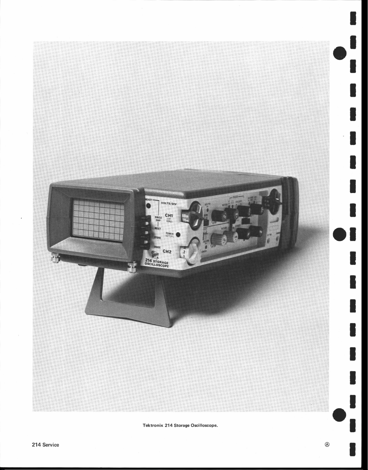
Tektronix
21
4
Storage
Oscilloscope.
o:
Page 7

I
Section
1-214
Service
fo
t
GENERAL
I
I
I
I
I
I
f
-
I
O
I The horizontal
I
I
I
.
I
t
I
I
I
I
The
Tektronix 214
portable
weight
measurements.
tions where
tional
mechanically
and other
provides
reduced
of the integral
automatically
rate.
channel with its
iffi :xl,,.ff
of vertical frequency
s1,\reep
division.
magnifier,
sliveep
division.
Sweep
faster.
horizontal
from
reduced
vertical
instrument that
with
display storage
(NONSTORE)
constructed
extremes
dual-channel
The
vertical deflection
bandwidth)
Single-trace
,,
rates
from
Uncalibrated
are
rate for
Stored
mode)
X-Y
operation is
deflection
less
than
bandwidth
deflection
the ability
lt is designed for
high-impedance
chop or
operation
position
i::lil"J
available
a maximum
Automatic Enhance
at sl,eep rates
one millivolt
of the
INFORMATION
Storage
associated
DC-to-500
to 50
alternate,
?l:ffJ
response.
deflection
500 milliseconds
$,\reep rates,
to at least five
provided
of the
of 50
applied
Oscilloscope is
combines
to make
general-purpose
is desired,
operation.
to withstand
portability.
with
kilohertz
factors
volts/division
is achieved
control.
from
probes.
depending
Single
?1,H",.
system
of
least
at
of 0.1 millisecond/division
with
Channel
applied
kilohertz).
(X)
to
50 volts/division
(Y)
INTRODUCTION
a solid-state
small
size and light
precision
along with
The
the
one millivolt
at the tip
The
by
turning
Sweep operation
waveform
applicaconven-
instrument
shock,
vibration,
vertical
of either
214
will either
upon the
off either
system
(at
srueep
is
'j;'#,^'J?lf
ffi
provides
to five microseconds/
via
a variable
times
the indicated
one microsecond/
occurs
Channel
signal.
(in
1 supplying
with
signal,
2
,Ji:
calibrated
$/eep
the
Single
and
the
a range
(at
supplies the
a
instrument
This
teristics after complete instrument calibration.
acteristics apply over an ambient temperature
-15oC
the internal batteries, and OoC to
when operating from an AC line source, except
indicated. Warmup
is
+55oC
to
will meet
(+5"F
for
time
the
+131"F)
to
given
following
+40"C
accuracies is
SPECIFICATIONS
Vertical Deflection
a
DEFLECTION FACTOR:
Calibrated Range:
in
steps
CAL
division.
between
factor to
BANDWIDTH
About two hertz
a 1-2-5 sequence.
Accuracy:
position
Uncalibrated
calibrated settings. Extends maximum
least
at
mV/DlV
10
5 mV/DlV:
2
mV/DlV: DC to at least 200 kilohertz.
1 mV/DlV:
Lower Bandwidth Limit, AC
Within 5%
(using
DC to at least 400 kilohertz.
DC
System
millivolt
One
with
VAR VOLTS/DlV
gain
and
(variable)
125 volts/division.
to 50 V/DlV:
to at least
at all
correctly
Range:
sixdivision reference):
DC to at least
100
def lection factors.
to
kilohertz.
(capacitively)
electrical
when operating from
(+32"F
50 volts/division.
set at
Continuously
five
charac-
These char-
range of
+104"F)
to
as otherwise
five
minutes.
control in
millivolts/
variable
deflection
kilohertz.
500
Coupled:
15
I
f.
I
The cathode-ray tube
Storage tube
division equals
The
internal
recharged
charger
@
having
0.203 inch).
214 is
operated either
rechargeable
from
(with
the
the
(CRT)
a 6 X
batteries.
power
AC
instrument
is
a direct-view
10 division
from
AC line
The internal
line by
OFF).
graticule
voltage or
batteries
the integral
bistable
(each
from
are
battery
INPUT RESISTANCE:
INPUT CAPACITANCE:
1 mV/DlV to
farads.
100 mV/DlV
farads.
mV/DlV:
50
to 50
One
megohm, within 5%.
Approximately 160
V/DlV:
Approximately
140
pico-
pico-
1-1
Page 8
I ntroducti
on-21 4 Service
MAXIMUM
50
volts
50
not
AC
nanoseconds.
CHOPPED
rate at approximately
ALTERNATE MODE:
rate,
INPUT
1Oo/o.
GAIN
with
gain
USABLE
V/DlV
peak-to-peak
mV/DlV to 1 mV/DlV:
over
MODE: From 500
IMPEDANCE MATCHING: Matched to within
ACCURACY BETWEEN CHANNELS: Within 5%
both VAR VOLTS/DIV
correctly
V/DlV:
to 0.1
AC
nruo kiloherlz or
set at 5
Triggering
TRIGGER
I nternal:
SENSITIVITY:
COMP: 0.2
division
INPUT VOLTAGE:
(DC + peak
volts
600
(five
megahertz
mVDIV
40 kilohertz.
From 1 mVDIV
controls
mV/DlV.
from
or
volts
600
risetime
to
to 5
in CAL
DC to 500 kilohertz.
AC).
600
less).
(DC
+ peak
less
not
2 ms/DlV of time
pslDlV
AC).
than 100
of time
position
and
Horizontal
SWEEP
Calibrated
seconds/division.
Accuracy
VAR HORIZ
correctly
of wveep
Linearity
divisions):
length).
Variable
brated
m icrosecond/d
one
1
CH
Calibrated
division.
Variable:
HORIZ
Accuracy:
CAL).
X-Y
Maximum Input
Deflection
RATE:
Range:
16 steps
(over
MAG control
1 mVDIV
at
set
length).
(any
trruo
Within
Magnifier; Continuously
settings.
HORIZONTAL
MAG}
Phasing:
Extends
Deflection
least
At
Within
Less
Display
System
milliseconds
500
1-2-5 sequence.
in
divisions): Within
eight
center
in CAL
(disregard
division
(disregard
5%
ivision.
INPUT:
five
1O%o
than 3o
Voltage: Same
portion
maximum
Factor:
times
(with
five kilohertz.
to
five micro-
to
5%
position
first
within center
first
lOo/o
variable
svveep
millivolt
One
magnification
VAR HORIZ MAG in
for
as
CH
and timing
microsecond
0.5
of total srueep
between cali-
rate to at
to 50 volts/
(using
(vertical).
1
with
eight
least
VAR
o:
I
I
I
I
t
I
ol
t
2:
CH
External:
PRESET
positive
above.
DISPLAY
hertz.
EXTERNAL
AC). 16 volts
slope
lnput Resistance: Approximately one
nput
I
Maximum
division
0.2
least
At
TRIGGER
of triggering signal.
JITTER: 0.5
TRIGGER:
Capacitance:
Usable Input
peak-to-peak
from
2 hertz to 500
volt from
one
LEVEL:
Approximately
Triggered
microsecond
Voltage:
(one
AC
1-2
kilohertz.
to 500 kilohertz.
DC
preset
at
Sensitivity
Eight volts
megahertz or less).
same as stated
or less at 500 kilo-
megohm.
picofarads.
30
(DC + peak
level on
GRATICU
Type:
Area: Six
Each
Stored Writing
millisecond
LE:
Internal
division
At least 80
equals
in
Black
divisions
0.203
Speed
divisions/millisecond.
Automatic
lsolation
f NPUT COMMON
battery
insulated
input common
volts RMS sinusoidal
$i,'
operated
?ily
I.'
cover.)
TO
with AC
Maximum
214 case
and
?li,H
line,
vertical
inch.
Enhance
214 CASE
700 volts
or
:$
i:
non-illuminated.
10 divisions
by
At least 500 divisions/
(internal
power
f loating
exterior
(DC
adjustment).
EXTER
plug
secured
potential
is not
+ peak
IOR :
to exceed
AC).
=#ff:ä,"
Jläl;:?.:"$f,ffi
B,
REV.
horizontal.
(When
the
in
between
500
1974
AUG.
I
I
I
t
I
I
o
t
I
Page 9
I
I
: O
I
sinusoidal
AC) is not to exceed 350
AC
or L4
,
Operation
times the
line voltage
AC
volts
plus
(DC
+ peak
Internal
BATTERIES:
Battery
Operation
rechargeable A
10
I ntrod u cti on
nickel-cadmium
size,
-21
4 Service
cells.
I
I
t
I
I
I
lo
I
Due
to
capacitive
the
changes may
age
transients.
sguare-wave
produce
LINE VOLTAGE
Stored
charged
between 104 and 110 volts
internal
Nonstore Mode: 104 to 126 volts AC.
operatd without
NE FREOUENCY:58
Lf
Refer
other
MAXIMUM
at 126 volts,
Avoid
inverter supplies,
large voltage
RANGE:
Mode: 110 to 126 volts
during AC operation.
batteries.
to
Option
Line Voltages
POWER
hertz.
60
line
input circuit,
cauffi damaging
operating this instrument
transients.
Instrument can be operated
with resulting slow discharge
resulting discharge of
to
62hertz.
NOTE
and Maintenance
and Frequencies.
CONSUMPTION:
sudden
input current
or other
AC.
sources that
Batteries
Instrument can be
internal
information
Three watts or less
volt-
from
not be
can
batteries.
for
of
(from
CHARGE
(instrument
POWER
indicates
left
BATTERY
strument
charge
TYPICAL OPERATING
after
NONSTORE
time
STORE
provided
TYPICAL
discharge
Table
TIME
off during
(BATTERY)
approximately
in
batteries.
the
EXCESSIVE
operation automatically
drops to 10
full charge cycle at
provided
Mode: 2.5
at
CHARGE CAPACITY
at
1-1 .
volts,
Mode: 3.5 to
lower trace
at
lower
trace
+20oC
to 3.5
to
charge
INDICATOR:
five
intensity.
line):
AC
minutes of scope
DISCHARGE
+0.5
volt.
TIME
+20oC
five hours.
intensity.
hours.
+30"C
hours
8
cycle).
interrupted
(at
maximum trace
+30oC):
to
Longest
(in
*68oF
or
for full
When
PROTECTION: In-
Longest
operating time
reference
to
charge
extinguished
operating
when battery
intensity
operating
charge/
to
+86oF)
life
St.
t
I
t
I
I
I
lo
REV.
ooc
+20"c
+40oc
APR.
C,
Charge
(+32"F)
+sgog
to
(+104"F)
1976
Temperature
(+68oF
to
+86oF)
TABLE
Operating
_lsoc (+soF)
1-1
Temperature
4OYo 6OYo
65Vo
40o/o
+20"G
(+69"F
+30"c
to
+86oF)
to
100% 85Yo
650/o
+55oC
(+131oF)
SOYo
55Yo
1-3
Page 10

I
ntroducti on-214
Service
Environmental
Temperature:
Operating from
+131"F)
Operating
+104"F)
Non-Operating,
Altitude:
Operating, to 25,000 feet
perature
feetl.
Non-Operating,
from
decreased
Batteries,
AC
Line, 0"C to
-40"C
to
by loC
50,000
to
per
-15"C
+ggog
feet.
to
(-40"F
(maximum
1,000 feet
+55oC
+40oC
(+5oF
(+32oF
+140"F)
to
operating tem-
above 15,000
to
to
Humidity
l;,'r1rl''.ätJ:
Shock
shocks
each direction
Physical
WEIGHT
DIMENSIONS
Height;
Width: 5.25
Depth:
(operating
(operating
at 150
along
(without
inches
3.0
inches
9.5
and
relative
e'o/o
non-operating): Tested
and
g,
one-half sine,
major axes.
accessories): 3.5
(measured
inches
at maximum
(7.6
centimeters)
(13.2
(24.1
non-operating):
humiditv in
millisecond
two
pounds
points):
centimeters)
centimeters)
f ive
cycle,
rererence to
with
duration
(1.6
kilograms)
nruo
O
I
:
I
I
I
I
I
I
I
ol
I
I
I
I
I
I
14
t
ot
@
Page 11
I
Section
2-214
Service
:O
I
I
I
I
I
I
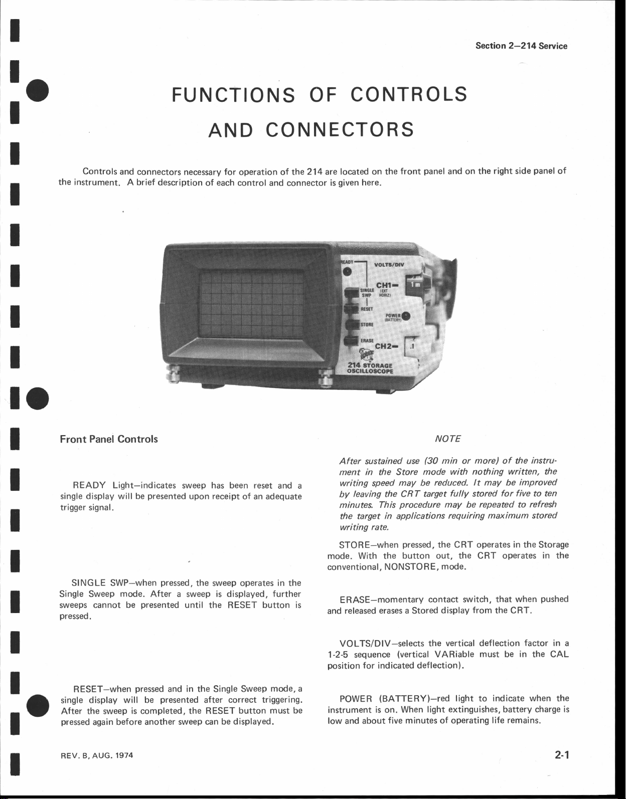
Controls
the instrument. A bri€f
and connectors
FUNCTIONS
AND
necessary for operation of the
description
of
each
CONNECTORS
control and connector is
OF
214 are located on the
CONTROLS
given
here.
front
panel
and on the
right side
pansl
of
lo
I
I
I
I
I
I
t
lo
Panel Controls
Front
READY
single
trigger
SINGLE SWP-when
Single
sweeps
pressed.
RESET-when
single
After
pressed
Light-indicates
display will be
signal.
Sweep
display will
the sweep
mode.
cannot be
before another
again
is completed, the RESET
presented
pressed,
After a
presented
pressed
and
presented
be
has been
sweep
upon receipt
the sweep operates in the
is displayed,
sweep
until
the RESET
in
the
Single
after
can be displayed.
sweep
reset
of an adequate
Sweep
correct triggering.
button
and a
further
button is
mode, a
must
be
After sustained
ment in the
writing speed
leaving
by
minutes.
target in
the
writing
STORE-when
mode. With
conventional,
ERASE-momentary
released
and
VOLTS/DlV-selects
1-2-5
sequence
position
instrument
low
for
POWER
and about
Store
may
the CRT
procedure
This
applications
rate.
the
NONSTORE,
erases
(vertical
indicated
(BATTERY)-red
When
is on.
five minutes of operating
NOTE
(30
use
pressed,
button out, the CRT operates
a
Stored
min or
mode
reduced.
be
target
may
the CRT operates in the
mode.
contact
display
the
VARiable
deflection).
light
more)
with nothing written, the
lt may be
fully
stored
repeated to
be
reguiring maximum stored
switch,
vertical deflection
light to indicate when the
extinguishes,
that
from
the
must
life remains.
instru'
of the
improved
for five
battery charge
CRT.
be
to
refredt
when
factor
in
the CAL
Storage
ten
in the
pushed
in
a
is
I
REV.
B, AUG.
1974
2-1
Page 12

Functions
Side
channel input
the
STEP ATTEN
the
deflection
Vertical POS-controls
appropriate trace. Detent turns the channel
VAR VOLTS/DlV-provides
deflection
VOLTS/DIV
the
PRESET trigger
of Controls
Panel
Controls
INPUT
frequency
The
large
AC
VERT
AUTO PREsET-screwdriver adiustment
TRIG
COUPLING-selects
signal to the
AC-DC
limit
GND-vertical
applied signal
resistor to
valve
input coupling capacitor.
DC-all
vertical system
entire
components of
vertical
amplifier
factors,
factor
switch.
GAIN-screwdriver
vertical system.
SOURCE-selects the source of the trigger
and
Connectory2l4
and Gonnectors
method
vertical
component
{-3
amplifier inpüt circuit is
BAL-screwdriver
for
between
point
for
input
of
point}
dB
is
connected to
provide a precharge
system.
minimum trace
AUTO
is
the input
vertical
the
a continuously
the calibrated settings of the
adjustment to set the
sl,\reep
used
amplifier
signal is blocked.
2hertz.
about
ground
signal are
adjustment to
shift when changing
operation.
Service
to couple the
system.
grounded.
through
path
passed
position
OFF.
to set the
Low
a
for
the
to
balance
of the
variable
gain
of
signal.
LEVEL/SLOPE-selects
the trigger
of
the indicator
triggered on
right of center,
the
LEVEL/SLOPE
detent, the srueep
on the
INTENs|TY-controls
SWP CAl-screwdriver
svveep timing.
POwER-controls
interrupt charging
instrument
FOCUS-screwdriver
display.
VAR HORIZ
sweep
the weep
HORIZ GA|N-screwdriver
gain
of the
Horizontal
trace.
signal on
dot
the
positive{oing
connected
is
magnification
indicated
rate
horizontal
POS-controls
which the sweep
is
to
positivegoing
on the
control is set to
is automatically
slope.
power
current
to an AC line
adiustment
MAc-provides
to a
system.
amplitude
the
left
the
brightness of
adiustment
to
maximum of
by the
or
slope of the trigger
negative€oing slope. When the
triggered at a
to
the
internal batteries when the
the
to
SEC/DIV
adiustment
horizontal
the
point
and slope
is
triggered.
center,
the
to
instrument. Does
voltage.
obtain
continuously
AUTO
the
CRT
provide
at least
sruitch.
to set the
position
the sweep is
preset
display.
calibrated
welldefined
a
five
When
signal; to
PRESET
level
not
variable
times
basic
of the
o:
I
I
I
I
I
I
^ I
I
U
t
I
I
I
I
COMP-sweep
the vertical signal after
of
2-sweep is
CH
of the CH
EXT-sweep is triggered from
applied
to
is triggered
triggered
2 vertical
EXT TRIG banana
the
2-2
from
a DC-coupled sample
the vertical switching.
from
an
AC-coupled sample
signal before the vertical
the DC-coupled
jack.
switching.
signal
SEC/Dlv-selects
the
detent
214
be in CAL
must
EXT TRIG-banana
between
under test.
ment
the
for
iack
and the
(VAR
rate
sweep
indicated
external signal
sweep
establish common
to
HORIZ
rate).
source or
MAG
ground
equip-
@
I
I
or
Page 13
I
_o
Section
3-214
Service
I
I
I
I
t
I
I
IO
I
I
I
I
I
Introduction
This
section
information
maintenance,
of the
use in
preventive
for
or
troubleshooting of
PREVENTIVE
General
Preventive
inspection, lubrication,
regular
ment
breakdown
instrument.
214
is
tenance.
maintenance
Avoid
might
Avoid
sodium hydroxide,
maintenance
preventive
basis,
The
subjected
A
convenient
preceding
is
the use
damage
chemicals
may improve
and
severity of environment
will determine the
CAUT'ON
of
chemical
plastics
the
which
or
Cleaning
The
214
conditions
can cause
The
dust in
lated
small brush.
and around
removed
and water
require.
component
high-impact
the
on these
with
solution.
should
interior
The
the exterior
a soft cloth
be
Accumulation
breakdown.
plastic
of
the
covers
can be removed
brush is
Abrasive
MAITUTEIUANGE
manual
MAINTENANCE
etc. When
maintenance
time to
recalibration
contain
sulfuric
cleaned
covers
instrument.
also useful
controls.
dampened
cleaners
contains maintenance
maintenance,
214.
the
consists
used
of cleaning, visual
performed
can
the
frequency of
perform preventive
of the
cleaning
in this instrument.
hydrochloric
acid.
as
often
of dirt in
provide
protection
Loose dust
with
for
dislodging
Dirt
that remains
in a mild
should not
sEcil0N
Lubrication
corrective
on a
prevent
reliability
to which
agents which
the instrument
a
instru-
of this
instrument.
acid,
as operating
against
accumu-
soft cloth
dirt
can
detergent
be used.
the
main-
or
on
be
require lubrication. No lubrication
the
reliability
sealed can
that does
Tektronix
Visual Inspection
defects as broken connections,
tors, damaged circuit
corrective
however,
components
trouble in the instrument; therefore,
the
damage.
CRT
following
this instrument:
intensity that is used,
rates, X-Y displays, or the
intensity
a
vertical
display area.
3
Generally,
contacts
The
overheating is important
Care
prolong
To
1.
Care
2. Avoid repeated use
particular
there are
rotary
or
potentiometers
of
be maintained by
not
affect
Part
No.
214
should
procedure
particular
found.
are
useful
the
precautions
must
be taken in the
permanently
may
display is being
position
occasionally to use other
006-2574-00).
be
boards,
for
care must be
Overheating usually indicates
should be
particularly
no components
should be used on
parts
of the
electrical
inspected
and heat
most visible
to
life
STORE
damage
of the same area
Stored
rotary
that are not
lubrication
characteristics
Do not over-lubricate.
occasionally for
improperly
damaged
defects is
taken
correcting
prevent
of the
Storage
observed
degree of writing-beam
when
mode.
the CRT screen.
repeatedly,
in the
with
recurrence
using slow sweep
214
that
switches. The
permanently
lubricant
a
(e.9.,
such
seated
transis-
parts.
The
apparent;
heatdamaged
if
other
the cause
of the
screen,
when
Too-high beam
the screen. lf
of
change the
portions
the
operating
of the
of
I
I
lo
I
Cleaning
sary.
The best
accumulated
brush
or a cotton-tipped
narrow
REV.
spaces
NOV.
C,
the interior
way to clean
dust
with
for
or
cleaning
1977
should
only
be
occasionally
the interior
dry, low-velocity
applicator
more
is
useful
delicate
is
blow
to
air.
A soft-bristle
for
eleaning
components.
neces-
off the
in
3.
Do not leave
no longer needed.
4.
Operate
required.
in
a Stored display
NONSTORE
the
on
the screen when
mode unless
it is
Storage
3-1
is
Page 14
Main ten
an ce
-21
4 Servi
ce
Recalibration
ensure accurate
To
instrument
this
of
To
probe
cases,
gain
wrap at
months
components
circuits.
localizing
in
minor
I nstructions
access
cords and
the
every six
ment of
affected
helpful
some
recalibration.
Disassembly
both
probe
I nformation
measurements.
each
after
if used
to
rear of the214.
infrequently.
necessitate
may
calibration
The
certain
troubles
may
the interior of
power
the
check the
1000 hours of
In addition,
recalibration
procedure
troubles
in
be revealed or
instrument,
the
from
cord
calibration
operation,
can also
instrument. In
the
corrected
instrument's
the
or
replace-
the
of
be
by
unwind
The arrows
direction
Fig. 3-1.
Remove
instrument.
instrument
the
circuit
pivoted
the
board,
out of
instrument
the
on
wrap
to
five screws
the
3-2. Separate
Fig.
See
lay it aside.
and
the
and
way.
the
now accessible
are
NOTE
probe
wrap
probes
the
in the
batteries,
Most of
proper
indicate
and
bottom
the
Power
The
can
internal
the
for maintenance.
the
power
cover of the
bottom
Supply
lifted
be
cord. See
cover
workings of
from
(A-3)
up an;d
o:
I
I
I
I
I
YELLOW GROUND
POSITIONED
HERE BEFORE
WRAP OF
THE
CLIP
PROBE
IS
FINAL
I
OI
I
I
I
I
I
I
I
3-2
Fig.3-1.
method
Proper
REV. APR 1974
for
wrapping
probes.
t
or
@i
Page 15
I
Maintenan
ce-214
Service
:o
t
I
I
I
I
I
I
lo
SCREWS
SECURING
SIDE
SCREWS SECURING
BOTTOM
PANEL
COVER
front
NOTE
panel
to
the lnput
pushbuttons
board
before
-
Secure the
and replace the
re-assem
Single Sweep board
bl ing th e instrum ent.
TROUBLESHOOTING
Introduction
following
The
troubleshooting
sectaons of
following information
component.
helpful
very
Description section
Troubleshooting
Diagrams. Complete
foldout
number
instrument are
the
designators
mentl. lmportant
on the
on
pages
and
Diagrams
diagrams.
circuit boards are
information is
214
the
manual
this
An
understanding of
in locating troubles. See
for more information.
Aids
in
the
electrical
shown on
section
identify components
to
used
voltages
The
provided
Information
should
to aid
Diagrams section. The component
value
portions
enclosed
.in
circuit diagrams are
of
the diagrams
for definition of the
waveforms
and
with blue
contained
be used along
locating the defective
the circuit operation is
each component
of
(see
the circuit
to
the
first
in this
are
lines.
facilitate
in
other
with
Circuit
given
in this
page
reference
instru-
shown
also
mounted
the
on
of
I
I
I
I
I
I
I
r
I
t
SCREWS SECURING
SINGLE SWEEP
Fig.
3-2.
Single
Single
the Power
removing
at a time,
(A-4)
panel
board to the
properly
Power
l^".*'J#:träJi:1":nJ:Hl
a
-
the Input circuit board and, with
the
Location
Sweep
For
calibration or troubleshooting
Sweep
the
board.
and the
connect the
Supply
lf access
panel,
front
BOARD
of
screws securing
(lnstrument
board.
(A-4)
circuit
Supply
(A-3)
panel pushbuttons
front
until they
Next, remove
two
screws
(A-1)
Input
circuit board.
front
to the
remove
bottom
shown
upside
board
should be
circuit board.
disconnect from
the
READY light
securing
circuit board.
Single
of the
the instrument
the
Sweep
Input
the READY
circuit board to
cover,
down.)
within
This
pulling
by
the
Single
(See
tA-l)circuit
[';:':ilJ';::lll
side
panel,
side
the 214, the
reconnected
is done by
them,
Single Sweep
from
the front
(A-4)
Sweep
Fig.3-2.)
panel.
board is
light
Then
out of
and
to
first
one
the
Troubleshooting
malority
The
214
can
be
such
262.
Type 577
conductor devices
in
thid
500 kilohertz
50 volt/division
Obtaining Replacement
Standard
replacements
local
many
obtained
them from Tektronix,
replacement
tolerance, rating, and description.
accomplished
Triplett Model
as a
dynamic
Use a
Transistor-Curve
instrument,
CORRECTIVE
Tektronix
of the
locally
Equipment
troubleshooting
of
with
630-NA
transistor
Tracer
used in the
use
a test oscilloscope
frequency
deflection
Parts.
for
the
Field
standard electronic
in
parts,
response and
factor.
MAINTENANCE
Parts
All electrical
214
can
Office or
less time
Inc.
Before
check the
a 20,000
tester such
214. To
be obtained
than
to be done on
ohms/volt
or a
Simpson
as a Tektronix
check the
to
check
with
millivolt
one
and mechanical
through
representative. However,
components can be
is required
purchasing
parts
or ordering
list for
the
VOM
Model
semi-
waveforms
a DC
to
to
part
your
to
order
value,
REV
DEC 1980
C
3-3
Page 16

-21
Maintenan ce
When
to remember that the
component
instrument. All
replacements unless it
component
performance.
4
Service
selecting
may
will not adversely
NOTE
replacement
physical
affect its
replacement
is known that a different
parts,
performance
parts
affect the instrument
is important
it
size and shape of a
in the
should be
direct
Ordering
Tektronix,
Instrument
1
.
2. lnstrument
3. A
description
circuit
number).
4. Tektronix
When ordering
Parts.
include
Inc.,
type.
serial
Part Number.
replacement
follovrüing information:
the
number.
(if
part
the
of
parts
electrical,
from
o:
include
I
Special
components,
214.
Tektronix, Inc.
ments,
cordance with our
parts
Tektronix,
local
Parts.
These
components are
or are
used
in this
Inc.
Tektronix
"o
some special
manufactured
Order all
Field
rrraro*
In
addition to the
components are
manufactured or selected by
meet
to
specifications. Most of the
instrument have
specific
special
Office or
/
SCREW
for Tektronix,
representative.
MOUNTED
standard
performance
been
parts
directly
ITTER
EM
electronic
used
in the
require-
Inc. in
mechanical
manufactured by
from
ac-
your
Disconnect
power
source
Component
Gircuit
given
beyond
on
in the
damaged
soldered
are
wired board.
WART'TG
instrument
the
before
Replacement
Board
Replacement.
repair, the
components
Mechanical
BASE2 Uilil
N.CHANNEL
from any
replacing
components.
lf a circuit
entire assembly
replaced.
be
can
Parts
List
ili-)
ffil
EMITTER
1
BASE
(}388
UNIJUNCTION
external
board
including all
Part
for
the completely
is
numbers
I
I
I
I
I
ol
t
I
coLLEcro-ffi
BASE
GATE
DRAIN
SOURCE
I
34
DUAL
EMrrrER
coLLEcro-,fi
SOURCE
DRA|N
GATE
Fig. 3-3. Lead
EMrrrER
eÄse
TRANSISTORS
14
14-PtN
INTEGRATED
configurations of semiconductors
coLLEcro-ffi
INDEX
C]RCUITS
EMrrrER
BASE
16-PtN
this instrument.
in
used
INDEX
,affi
1
ru-r^J-J
1483-04
or
1981
E DEC
REV
I
I
I
I
I
Page 17

I
Mai ntenan
e,e-21
4
Service
:o
I
I
I
I
I
I
I
I
o
I
I
I
Transistor Replacement. Transistors should
replaced unless actually
sockets during
original sockets.
may affect the
transistors
the instrument which
of
Replacement transistors
or a
type
configuration
Some
which do
tor is replaced by a
different
plastic
manufacturer's basing diagram
transistor sockets
basing used for metal-case transistors.
An extracting tool should be used
16'pin
pins.
one
both ends
disengage
be
semiconductor's index with
do
flat
lf an
these integrated
of
damaged.
will result
so
routine maintenance, return
Unnecessary
are replaced, check
direct
of the transistors used
case
not
agree
manufacturer
integrated circuits
extracting
of the device.
from
the socket before
When
in damaged components.
il: i:f,j#r
replacement
Power
ment from
necessary
C212 to maintain
and
Refer
three
quency
parts.
Supply
power
sources
change
to
Table
to
of the
3-1
more commonly used line voltage/line
combinations.
defective.
callbration
may
replacement.
transistors
with those shown
transistor
than the original,
in this
instrument
is not
tool
circuits,
Avoid
replacing
that
.'ilr"[+ *,Fj:r:'"l;#i#
Gapacitors. When
other
electrical
the
proper
for
the
correct
lf removed
replacement of transistors
this instrument.
of
the
operation
be affected.
strould be of
Fig. 3-3
in this instrument.
have lead conf
which is
for
correct
are
remove
to
prevent
to
available
pull
slowly
having
one
the
other,
semiconductors, key
the socket. Failure
of
operating
1 15
than
value
of
current leve.ls to the batteries.
values
of
not be
from,
them to
When
of that
the original
shows
here.
VAC
the
igurations
lf
a transis-
made by a
check the
basing.
for
wired
14-
the
damage
when removing
and evenly
end
as the
capacitors C210
capacitance
to the
of the
pins
the instru-
Hz, it is
60
their
their
part
lead
All
the
and
on
l.C.
may
the
to
for
fre-
Due
voltage changes
sients.
wave
large
Selection
frequency
3-4 and
ated on a
minimum
to the
instrument.
the
values of C210 and
provides
selected
ratings should be at
applied
C2O4
nominal
from other
24OV 5O
with
Selectable
selected
than
change
The value of
330
1. Install a 27O
the capacitive
to
Avoid
operating
inverter supplies,
vol
tage transients.
capacitor
of
combinations
For example,
3-5.
Hz line,
60
maximum
and
pF
3.3
.OO1
1.5
O
as
set SEC,/DIVto
(fully
capacitance
lt
Hz information.
50
from
a type suitable
voltage.
line
and C215
value only
1 15V
than
Hz operation, C2O4
gF
3kV capacitors.
Gomponents.
f
a switching
or
divisions
when
follows:
for each channel
changing
R388 is
clockwise).
also
when
power
may
cause
this
or other sources that
values
is illustrated by the
if
graph
the
line voltage limits, with
values,
provides
for
C212
least 1.414 times the
values
the
Hz or 1 15V 60
50
unblanked trace
sweep
selected
O resistor for R388, turn the
.5 s, and
line circuit, sudden
damaging current tran-
instrument
for
instrument is to be
the
in
for
information
other
These
for AC
must be changed
instrument
C215 should
and
Resistor R388
and
speeds
from
a
INTENSITYto
set
from
produce
line voltage/line
other
graphs
Fig.3'5 illustrates the
proper
operation
for
voltages. Fig. 3-4
line
capacitors should be
operation
minimum intensity
from 5 ms
range
and
value
is
to be operated
power
Hz
be
height of
27O,3OO, or
oI
square-
Figs.
in
oper-
respect
of
selecting
voltage
of the
from the
For
line.
replaced
value is
no more
ms.
2
to
214 on,
maximum
il
I
I
I
lo
I
Nominal Power
Voltage/Frequency
1 10 to 126 VAC
58 to 62
(Standard)
90 to 1
48
to
(Option
224 to 250
48
to 52
(Option
1981
F DEC
REV
TABLE 3.1
POWER SUPPLY CAPACITORS
Line
c210 - c212
+10%,2O0
pF,
3.3
Hz
10 VAC
Hz
52
2)
Hz
1)
VAC
VDC Tektronix
PN
285-0925-00
+1O%,200
4
ttF,
VDC Tektronix
PN
285-0935-00
+1oo/o,4OO
2
ttF,
VDC Tektronix
PN
285-0933-00
The
2.
the CH
set CH
horizontal
Check
3.
trace
lf each unblanked
4.
divisions, turn offthe214,
R388, recheck and
for
unblanked
high while
when
will show as
traces
1 dot
2 POS to
graticule
that
elftends
switching
the top
to
no more than
vertically
traces
maintaining
dots. Set CH
horizontal
place
the CH 2 dot to the
li ne.
1.5 divisions of unblanked
from each dot.
exceeds
trace
installthe next
repeat steps
are no more than
minimum
from 5 ms to
sweep
speed
POS
1
graticule
2through 4 until
1.5 divisions
intensity
place
to
line
bottom
1.5 vertical
larger
change
2 ms.
3-5
and
size
Page 18
Maintenan
ce-214 Service
Recalibration
After
any electrical component has been replaced, the
calibration
well
as
circuits.
calibration
work has been
I nstrument
lf
Tektronix
the
Service Center
(wittr
owner
firm
that
number
and
that
of
the calibration
as
Since the
the
of
Repackaging
for
address) and
can be
a description
After Repair
particular
power
instrument
entire
in the
done
instrument is
service
contacted,
supply.
or
the name
of the
circuit should be checked,
of other closely related
supply affects all circuits,
should be
be shipped
to
repair,
attach a tag
of an
complete
service required.
checked if
Tektronix
to a
showing:
individual
instrument serial
at
your
Save and
shipped.
available,
The carton test strength
re-use the
lf
the
repackage the
Surround
protect
corrugated
having inside dimensions
than
by tightly
foam between
carton
the
the instrument
with shipping
package
original
the instrument
finish
of the
cardboard of
packing
three inches
carton and
in which
packaging
instrument as
with
instrument.
the correct
of
dimensions.
instrument, on all sides.
or industrial stapler.
tape
your
for
your
is unfit
follows:
polyethylene
Obtain a
carton strength and
less
no
than
Cushion the instrument
dunnage
of
instrument is 200
instrument was
for
sheeting to
inches more
six
or
use or
carton of
urethane
Seal
pounds.
not
I
I
-
I
V
I
I
I
I
r
I
I
I
I
I
ol
I
I
I
I
I
I
3-6
REV E DEC
o:
1981
Page 19
I
:o
I
I
I
I
UJ
gs
Ftr
J tt,
ot
>ö
uJ>
Zz
180
160
:
in non-store
mode, without
Maintenan
ce-214 Service
I
I
I
lo
I
I
I
I
lrJ
s9
dz
ljE
!
JO
e5
-o
LU>
V=
J
120
100
180
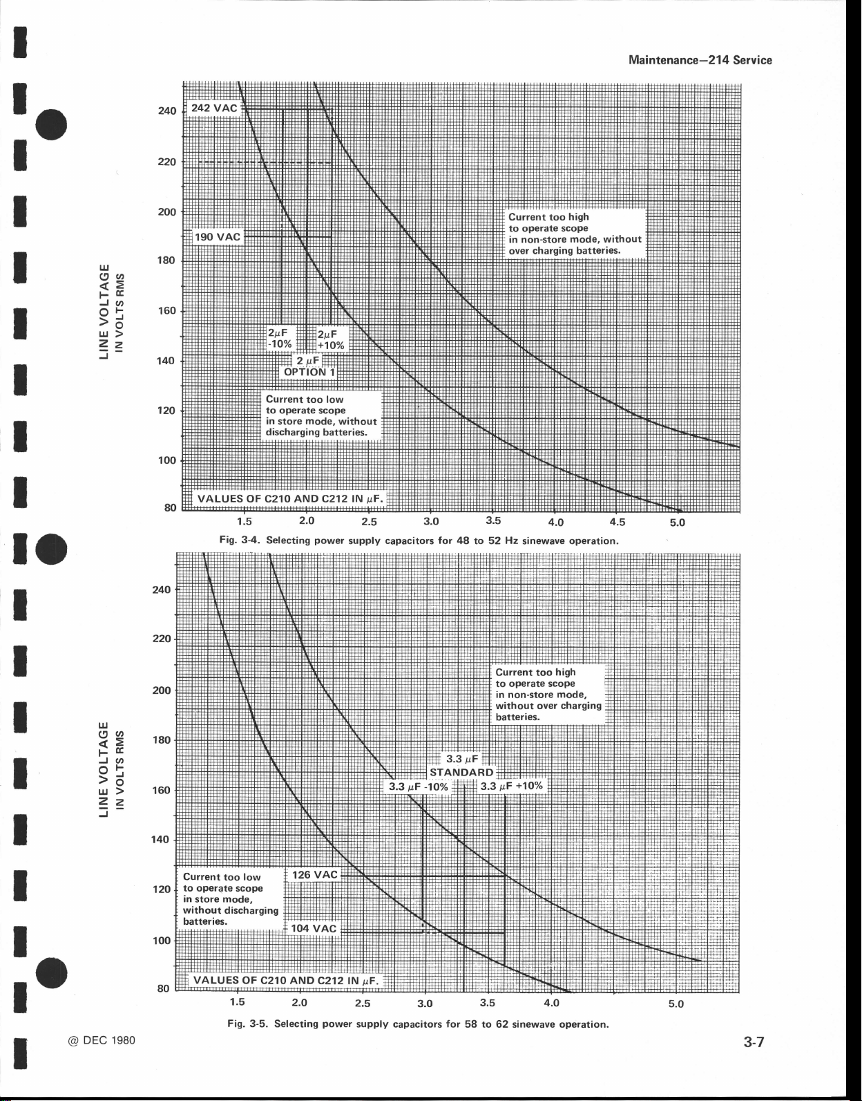
Fig.
Current
to operate scope
in
discharging
1.5
3-4.
Selecting
store
too
mode,
2.O
power
low
without
batteries.
supply
2.s
capacitors for
3.0
3.5
48 to 52
Hz
Current
operate scope
to
in non-store
without over charging
batteries.
4.o
sinewave
high
too
mode,
4.s
operation.
I
I
I
lo
t
DEc 1e8o
@
140
Current
to
120
100
operate
an
store mode,
without discharging
batteries.
low
too
scope
1.5
Fig.
3-5. Selecting
2.O
2.5
power
supply capacitors
3.0
3.5 4.0
for
58 to 62 sinewave operation.
3-7
Page 20

o:
I
I
t
t
I
I
ol
I
I
I
I
I
I
o:
Page 21

I
:o
Section
4-214
Service
I
I
I
I
I
I
r
I
I
f
I
General
ensure
To
the 214 every
if
used
infrequently.
oughly
Preventive
recalibration
Service
or
ensures
ilff ff : il,,"#l,
O
before an adjustment
performance,
even
clean and inspect
Tektronix,
Center.
representatave
Completion
that
the
if
CHECK-
instrument
1000
hours
Before
Maintenance
Inc.,
at local Field
Contact
of
this instrument
lälJo,
make
section.
provides
for further
each
J
l,
each
step
CALIBRATION
accuracy,
of
this
complete
Service
your
step in
" iil
i,"''}I
is
adiustment
is
within the
check the
operation, or every
complete
instrument
local
information.
the
made. For best overall
calibration,
as outlined
instrument repair
Centers and the Factory
Tektronix
Calibration
meets
ll,?y;
the
Il
to
the exact setting
allowable tolerances.
calibration
six months
thor-
in
and
Field
Office
procedure
electrical
g-*
;J""[ä
of
the
TEST
following
The
equivalent,
214.
Given specifications
minimum necessary for
specifications of any test equipment
exceed
be
specifications.
units
instruction
mation
Special Calibration Fixtures
procedure
These special
Tektronix,
Tektronix Field
those
correctly calibrated
are
is needed.
Special
only where
EOUIPMENT
test
required for
are
listed below.
Detailed
given
not
manual for
Tektronix
calibration
Inc.
Order by
Office
REOUIRED
equipment
accurate
and operating
operating instructions for
in
the
Calibration
they
part
representative.
or
and accessories,
complete
for
the test
calibration.
All test
this
facilitate
equipment
procedure.
equapment
test
fixtures
fixtures
number
instrument
calibration
equipment
Therefore,
must
either meet
is
within
Refer to the
if more infor-
are used
are
available
through
or their
of the
are the
the
or
assumed to
listed
the
the test
in
this
calibration.
from
your
local
I
I
1.
DC Voltmeter
I
I
I
I
2.
Co nstant-Amplitude
Signal Generator
l;.1?lilll*of;'0".
lro
@
Description
Low-Frequency
Range, zero
accuracy,
impedance,
Frequency,
500
tude,
Ampf itude
signal
volts
signal,
wave.
within
kilohertz;
least 200 millivolts.
at
amplitude,
to 100 volts;
one-kilohertz
to 1000 volts;
3o/o; input
20,000 O/volt.
kilohertz
one
output
accuracy, O.25o/o;
five
to
ampli-
milli-
output
square
TABLE 4-1
Test Equipment
Power
checks, CRT Grid Bias,
age Level adiustments. Vertical
adjustments.
Storage Enhance
ment.
bandwidth
tion checks.
Vertical and
checks
Supply
horizontal
and
Vertical amplifier
and adjustments.
output
centering
Level adjust-
and trigger
horizontal
opera-
level
Stor-
gain
Example
Triplett
Simpson Model 262.
a. General
Tektronix
a..
Model
Radio 1310-B
Part
630-NA.
Oscillator.
No. 067-0502-01.
+1
Page 22

Caf i brati o n
-21
4
Service
Description
4.
Square-Wave
Generator
5.
Time-Mark Gen-
erator
6. Ramp Generator
7.
Attenuator Ratio,
8. Cable
9.
Adapter Connectors,
10. Adapter Co
Minimum
F requency,
risetime, 100
fess;
output
volt to 40 volts.
Marker outputs,
nd s
seco
marker
O.1o/o.
F requency, ät
microseconds;
tude, at
nal
triggering, both AUTO
and NORMAL.
impedance,
lmpedance, 50
RG-58/U;
connectors,
female.
n n ectors,
BNC.
Specifications
one kilohertz;
nanoseconds
amplitude, o.4
five
0.1 second;
to
accuracy,
least 100
output
least
10X; connectors, BNC;
volts;
six
O.
S0
O; type
length, 42
BNC.
GR874 and
probe
or
micro-
within
ampli-
exter-
inches;
BNC
tip-to-
TABLE
Vertical amplifier
tion checks and
Horizontal
adiustment.
Hum Balance
Storage
ment. Vertical
bandwidth check.
E
check.
Vertical amplifier
tion
Used
for
(contl
4-1
timing
Enhance
xternal
signal
trigger operation
checks and adjustments.
throughout
interconnection.
Usage
compensa-
adiustments.
checks and
adjustment.
Level
amplifier
comp€nsa-
procedure
adiust-
Example
Tektronix Type
a.
Generator.
a. Tektronix
Mark Generator.
b.
Tektronix
Generator.
a. Tektronix
Generator
Power Supply.
Tektronix
a.
a. Tektronix
Tektronix
a.
Tektronix
a.
Type
Type 183 Time-Mark
Type RG 501 Ramp
with Type TM
Part No.
Part No. 012{057-01.
Part
Part No. 013-008401
106
Square-Wave
2901 Time-
501
1-0059-02.
01
No.017-006300.
o:
I
I
I
I
I
I
ol
I
11 . Adapter Connectors,
banana
12. Termination lmpedance,
2o/oi
13. T-Connector Connectors,
14.
Screwdriver
1 5. Low-Capaci-
tance Screwdriver
Three-inch shaft;
bit.
plug.
connectors, BNC.
1
1/2-inch shaft.
+2
BNC
Cl;
50
BNC.
female-to-
accuracy,
3132 inch
External trigger
Vertical amplifier
tion checks
External trigger
throughout
Used
to
adjust
Used to adiust
citors.
checks.
and adjustments.
checks.
variable
resistors.
variable capa-
compensa-
procedure
a. Tektronix
a. Tektronix
Tektronix
a.
Xcelite
a.
a. Tektronix
R-3323
No. 103{090{0
Part
No.
Part
Part No.
Part No.003{000{)0
10049-01 .
01
103003000
REV
B APR
1980
I
I
I
I
I
o:
I
Page 23
I
Cal i brati o n-21 4 Service
I
-
I
I
I
I
I
I
I
I
O
-7
This instrument
temperature
1.
Remove
Disassembly
section.
2.
Connect
source. lf the batteries
connected
period
for
a
with calibration.
3.
Set
liminary
warmup before
Titles
fully
capitalized
SWP). lnternal
(e.9.,
Grid
PRELTMTNARv
should be
(ts"C)
+25"C
of
the
instrument
Instructions in
the instrument
are not
to the
the instrument
Control
for
line
with
of approximately
Settings. Allow at least
proceeding.
external controls
in this
adjustments
Bias).
pRocEDURE
for
the
fully
the
one hour before
controls
NOTE
procedure
are initial
adiusted at
best
overall accuracy.
covers as described
Preventive
to a 117 VAC,
charged,leave
power
as
of
this
an ambient
Maintenance
60 Hz
the214
switch
turned
continuing
given
under
five
minutes
instrument
(e.g.,
SINGLE
capitalized only
in the
line
OFF
Pre-
of
are
Storage Controls
STORE
ERASE
Channel
VOLTS/DIV
VAR
VOLTS/DIV
POS
INPUT COUPLING
Channel 2 Controls
VOLTS/DIV
VAR VOLTS/DIV
POS
INPUT COUPLING
Trigger Controls
TR IG
LEVEL/SLOPE
RCE COMP
SOU
Out
{NONSTORE
Out
1
Controls
5m
(detent)
CAL
Midrange
GND
5m
(detent)
CAL
(detent)
OFF
GND
AUTO PRESET
mode}
(detent)
lo
I
I
I
I
I
I
PRELIMINARY
Preset
below
when starting calibration.
SINGLE
RESET
instrument
the
SWP
Single
Sweep
CONTROL
controls
Gontrols
SETTINGS
to
Out
Out
the settings
given
SEC/DIV
VAR
HORIZ
POS
POWER
INTENSITY
Sweep Gontrols
MAG
Display Gontrols
1m
(detentl
CAL
Midrange
ON
ly
Ful
counterclockwise
!r
I
@
+3
Page 24

Calibratio n
-214
Service
Equipment Required
1.
2.
3. Low-Frequency Constant-Amplitude
erator
Control
Preset
Prel iminary
Check
1.
lf
prior
Generator
Ramp
Voltmeter
DC
(General
the instrument has
Radio
Settings
.instrument
Control
Power
to recalibration,
(TM
1310-8
controls
Settings.
Supply
proceed
501/RG
Oscillator)
the
to
DC Levels
NOTE
been
operating
with
501)
settings
step
POWER
ntisfactorily
2.
SUPPTY AND DISPLAY
Signal Gen-
given
under
4. Probe
5.
6. Three-inch Screwdriver
Supply
-5.6
+5.6
+65
-1000
b.
To measure the
tip-to-BNC
10X BNC Attenuator
Power
V
V
V
v
Adapter
TABLE
Supply
-5.6
+5.6
+65
-960
(due
-100
4.2
Accuracy
Measurement
10.4
volts
10.4
volts
t4
volts
to
V
supply:
volts
140
volts
meter loading)
volt
volt
volts
o:
I
T
I
I
I
I
ol
a.
Using
power
pofarity.
supplies
the DC Voltmeter,
given
in
See
Fig. 4-1
tor
Table
test
measure
4-2.
point
Fig. 4-1.
the DC level of the
(A)
proper
Location
Observe
locations.
meter
of
Grid Bias adjustment
1. Depress the
Measure
2.
-110
to
volts
3. Press the
(B)
and
the
volts
STORE
Power
STORE
-100V
(see
button
test
supply
button.
supply
4-21.
Fig.
points.
release
to
for
reading
a
it.
of
t
-95
I
I
I
I
I
o:
4-4
REV. B, AUG.
1974
Page 25

I
Caf i brati o n
-21
4
Service
:o
I
I
t
I
I
I
I
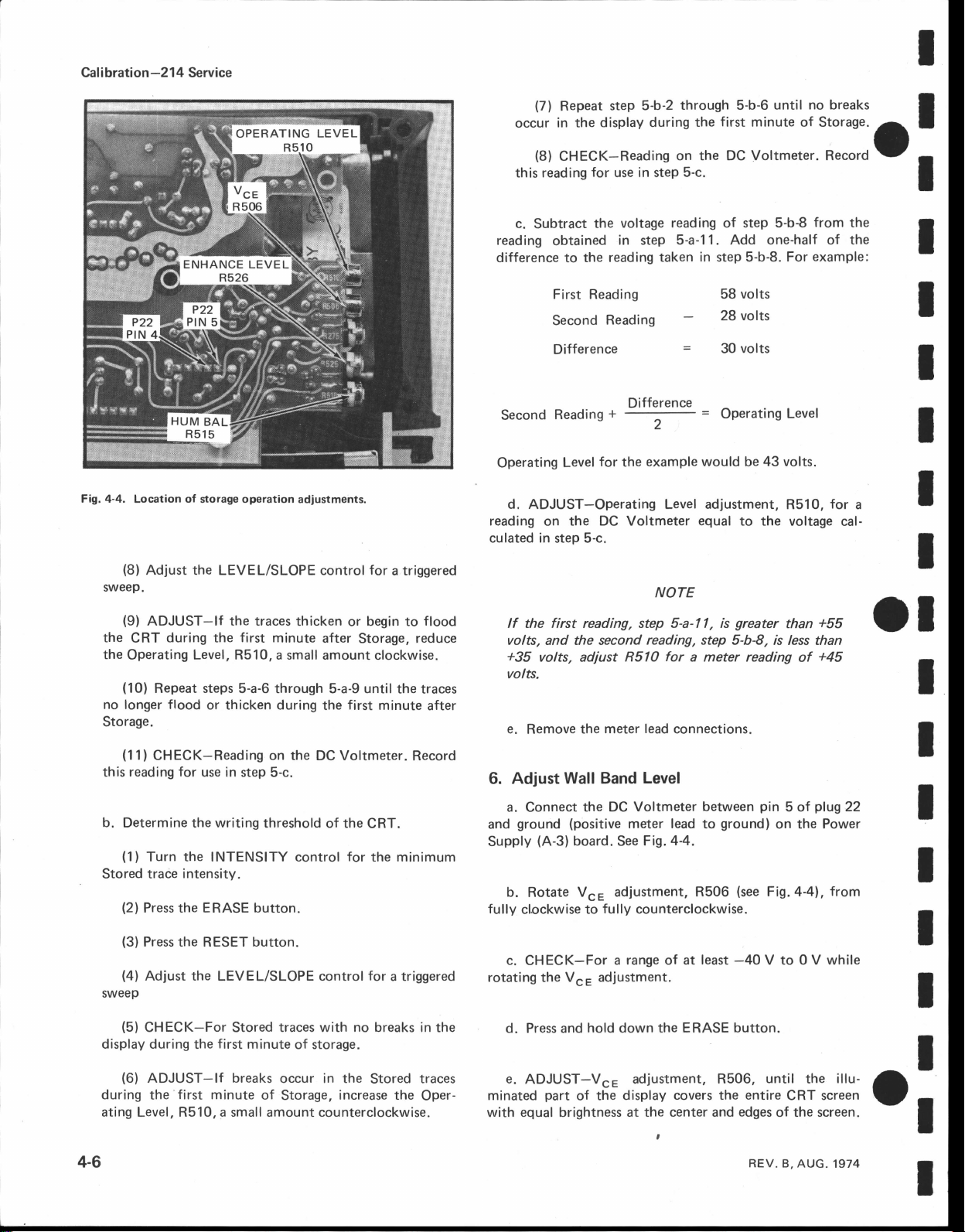
Fig.
*2.
Location of
-100
2. Adjust CRT Grid
a. Connect the
plug
of
Supply
P3
Board
DC
(negative
(A-3).
See
point.
tost
V
Bias
Voltmeter
meter lead
4-1.
Fig.
between
pin
to
2)
pin
on the Power
5
and
ptn
b. Position
line.
c.
CHECK-Free-running
horizontal
d. ADJUST-Trace Rotation adjustment, R141
Fig.
graticule
2
graticule
4-3)
to align the
line.
the
trace to
I ine.
the
sweep with the
center horizontal
$/\,eep is
parallel
center
graticule
with the
(see
horizontal
lo
r
I
I
I
I
I
I
I
I
I
b.
Turn the
c.
CHECK-Meter
d. ADJUST-CRT
rneter reading
e.
Disconnect
fully
trol
Adjust FOCUS
3.
Turn the
a.
POS control to the
b.
Set
INTENSITY
c. ADJUST-FOCUS, R398
panel)for
INTENSITY control fully
reading
Grid Bias adiustment, R273,
+1.9
of
counterclockwise.
the
control
welldefined dot.
a
volts.
meter leads.
POS
2
CH
OFF
SEC/DIV
for a nominal
clockwise.
+1.9
of
control to midrange and
detent,
switch to X-Y and
volts.
Turn the INTENSITY con-
display
(located
intensity.
on the
for
a
the
CH
adjust the
214
side
Fig.
4-3.
Location
5. Adiust Storage
a. Determine
(1)
vertically
graticule
(21
1
INTENSITY
(3)
tg. 4Al
F
(41
and
22
Power
(5)
button.
of Trace Rotation
Operating
upper writing
the
1 POS
Turn the
position
divisions.
Set
PREsET-Operating
f
ul
Connect
ground
Supply
Depress
CH
two traces within
the
the
SEC/DIV
fully
control
ly
counterclockwise.
the
{negative
(A-3)
the
clockwise.
DC Voltmeter
meter lead
board. See
SINGLE
switch
adjustment.
Level
limit
of the CRT.
control
to 5 m and turn
adjustment, R510
Level
between
Fig.4-4.
button and the STORE
SWP
midrange
to
the center
pin
ground)
to
4
of
on
and
four
the
{see
plug
the
4. Adjust Trace Rotation
- O
I
I
a. Set the
l@
SEC/DIV
switch to 1
m.
(6)
Press the
(7)
Press the RESET
ERASE
button.
button.
4-5
Page 26
Cal i bration-214 Service
I
Fig.4-4.
sweep.
Location
(8)
Adjust the
of
storage operation
LEVEL/SLOPE control
adjustments.
for
a triggered
(71
Repeat
in the display
occur
(8)
CHECK-Reading
this reading
c.
Subtract
reading
difference to
Second
Operating
reading on the DC Voltmeter
culated in step
obtained
First Reading
Second
Difference
Reading*
d.
ADJUST-Operating Level adjustment, R510,
for
the
the
Level
5-c.
step 5-b-2
use in step
voltage reading of step 5-b€
in step
reading taken
Reading
Difference
T=
for
the
through
during
on the DC Voltmeter. Record
5-c.
5-a-1
example would be 43
NOTE
s-b-G
first
the
1.
Add one-half of the
in
step
volts
58
28 volts
volts
30
OperatingLevel
equal
to the voltage
until no breaks
minute of Storage.
from
the
volts.
example:
for
a
cal-
5-b-8. For
|!
^-.
I
I
I
I
I
I
I
I
(9)
ADJUST-|f the traces
the
the
no longer
Storage.
this
b. Determine
Stored trace
sweep
display during
during the first minute
CRT
Operating
(101
(11)
reading for
(1)
Turn the
(2)
Press the ERASE button.
(3)
Press the
(4)
Adjust the
(5)
CHECK-For
Level, R510, a small amount
Repeat
CHECK-Reading
steps
flood
use in
the
intensity.
RESET
the
or
thicken
5-a-6 through
thicken during the
on
the DC
step 5-c.
writing
INTENSITY control
threshold
button.
LEVEL/SLOPE control
Stored
first
traces with no breaks
minute
of storage.
or
after
5-a-9
first
Voltmeter. Record
of the
for
reduce
the traces
minute
triggered
a
flood
after
in the
begin to
Storage,
clockwise.
until
CRT.
the minimum
for
lf the first reading, step d-a-l l, is
volts, and the second
+35
volts, adjust R5l0
volts.
e.
Remove
the meter
6. Adjust Wall
a.
Connect
ground
and
Supply
b.
Rotate
fully
cllcckwise to
c.
CHECK-For
rotating the V"= adiustment.
d. Press and
the DC Voltmeter
(positive
(A-3)
board.
V", adjustment,
hold
reading,
for
lead
connections.
Level
Band
meter lead
Fig.44.
See
fully
counterclockwise.
a range of at least
down the
greater
5-b-8,
step
a meter reading
between
to
R506
ERASE button.
pin
ground)
(see
Fig.4-41,
-40
V
+55
than
is less than
+45
of
plug22
5 of
the Power
on
from
to 0 V while
ol
I
I
I
I
I
I
(6)
ADJUST-|f breaks
during
ating
first
the
R510, a small
Level,
minute
occur in the
of
Storage,
amount
counterclockwise.
Stored traces
increase
the
Oper-
e.
ADJUST-V"=
minated
with
part
equal brightness at
of the
adjustment. R506,
display
covers the
the center and edges
until
entire
CRT screen
of the screen.
4-6 REV, B,
illu-
the
AUG. 1974
o:
I
Page 27

I
Gaf ibratio
n
-21
4
Service
:o
I
I
I
I
I
I
I
f.
Release
g.
CHECK-For
h.
Release
Adjust Enhance
7.
a.
Set
sruitch
the INTENSITY control
1 POS
CH
b.
Connect
Low-Frequency
Xl0
BNC
c. Adjust the
nal
Generator
d. Depress the
the
STORE
tne
SEC/DIV
to
2,
CH
the
control to the
the
Constant-Amplitude
attenuator
for
ERASE
uniform
and
Level
CH
CH
and a
Low-Frequency
3.2-division
a
SINGLE
button.
erasure
SINGLE SWP
switch to
2INPUT
for
OFF
2
COUPLING switch to AC,
visible
a
detent.
probe
tip to the output
probe
tip-to-BNC
display
SWP and
of the CRT
the TRIG
5p,
display, and
Signal
Constant-Amplitude Sig-
of a
STORE
screen.
buttons.
SOURCE
Generator via a
adapter.
kHz
50
buttons.
turn the
the
of
signal.
b.
Connect
the Ramp
c. Set the Ramp
six-volt, 100
and a
d.
Using the CH
display to
the
e.
Center
f
. Set
g.
Connect a
Ramp Generator to
the
h.
Adjust the
stable display.
i.
ADJUST-Hum
horizontal def lection.
the
CH
Generator.
!ts,
2
write the
the display on the CRT
the
Generator
Ramp
Xl
Ramp Generator Triggering
probe
2
Generator
ramp
output.
horizontal
and
entire
probe
from
the test
Bal adjustment, R515,
to
tip
the
for
External Auto Triggering
POS controls,
screen.
CRT
graticule.
for
Normal Triggering.
the External lnput
point
shown in
Ramp
Fig. 4-5.
controls
for
output of
position
of
iack
for
minimum
a
lo
I
I
t
I
I
t
Press
e.
f.
Press
g.
ADJUST-Enhance
Fig. 44)
h.
Press the
i.
CHECK-Entire
Disconnect the test
i.
8. Adjust
a. Set
VOLTS/DIV switch
ERASE button.
the
the RESET button.
for
best
the
RESET
Hum Balance
the
the
SEC/DIV
Level
possible
CRT screen
to
display.
button
setup.
switch to
2.
Wait
5 seconds.
adjustment, R526
several times
may be
in
flooded
and the CHz
X-Y
(see
succession.
positive.
Fig. 4-5.
point
test
Location
for ramp
of
Hum
generator.
Balance adjustment, and
external
trigger
lo
I
REV.
B, AUG.
1974
4-7
Page 28

Galibratio n-214 Service
Equipment
1.
2.
erator
3.
Standard
4.
Square-Wave Generator
5. Probe tip-to-BNC
Required
DC Voltmeter
Low-Frequency
(General
1310-B
Radio
Amplitude
Constant-Amplitude
Oscillator)
Calibrator
(Type
Adapter
Gontrol Settings
Preset instrument
Preliminary
INTENSITY Visible
Control
9. Adjust Vertical DC
a.
Connect
the
on
11)
the
Amplifier
ground.
and
b.
Adjust the CH
meter.
controls to the settings
Settings,
except
Centering
the
DC Voltmeter between
(A-2)
See
board,
Fig. 4-6.
1 POS
(positive
control
Signal
(067-0502-01
106)
given
follows:
as
Display
pin
11
meter lead
for
a 0 volt reading
VERTICAL
Gen-
)
under
of
U105,
pin
to
on
SYSTEM
BNC
Attenuator
Adapter
Screwdriver
Screwdriver
should
center.
Centering,
center
meter
leads.
GR-to-BNC
6.
7 . 10X
{.l BNC Termination
8. 50
9.
Three-inch
1
0. Low-capacitance
c.
CHECK-Trace
division of
d. ADJUST-Vertical
position
e.
graticule
trace to the
the
Disconnect the
10. Adjust Ghannel 1 Step
a. Rotate the
1m.
b.
CHECK-The
vertical
50mto1m.
trace shift
CH 1 VOLTS/DIV
display
CRT
between adjacent switch
be within
horizontal
approximately 0.4
R101
Attenuator
switch
for
0.1 division,
(see
Fig.4-61 to
graticule
Balance
from
or less,
positions
line.
50
o:
T
I
I
I
t
I
ol
m to
I
of
from
I
Fig.
4-6. Location of
4-8
Vertical
Centering adjustment
and
test
point.
c. ADJUST-CH 1 STEP
on the side
the
CH
11. Adjust
a. Turn
POS control
b.
1m.
c. CHECK-The CRT
vertical
50mto1m.
d.
the side
on
the
CH
panel)
1 VOLTS/DIV
Channel 2 Step
the CH
midrange.
to
Rotate
ADJUST
the CH
trace shift
-CH2
panel)
2 VOLTS/DIV
for minimum
1 POS control to
between adjacent
for minimum
switch
ATTEN
from
BAL, R417
trace shift when
50 m to 1 m.
Attenuator Balance
OFF
2 VOLTS/DIV switch
for
display
ATTEN BAL, R315
STEP
from
switch
0.1 division,
switch
trace shift when
50 m to 1
(locatäd
rotating
and the
from
50 m to
less,
or
positions
(located
rotating
m.
CH
of
from
@
I
I
2
I
I
I
a
-
I
I
Page 29
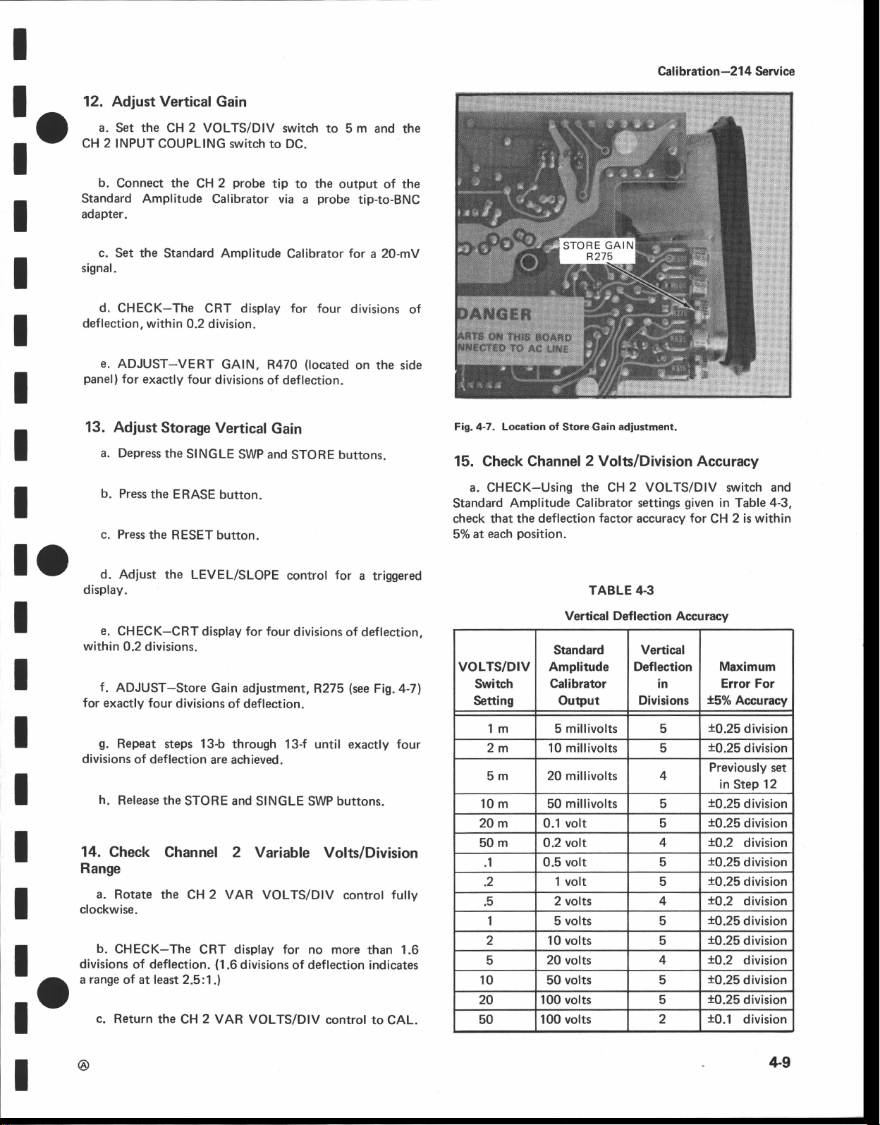
I
Caf
i bratio n
-21
4
Service
I
:
I
I
I
I
t
I
I
O
12. Adiust Vertical
cu" äill.i?'.SiÄ
b.
Connect
Standard Amplitude
adapter.
c.
Set the
signal.
d.
CHECK-The
deflection, within
e.
ADJUST-VERT
panel)
for
13.
Adjust
a.
Depress
b.
Press
c. Press
the
Standard Amplitude
exactly four
Storage
the
the
ERASE
the RESET button.
Gain
X,?1TIilY"'#':^
probe
2
CH
Calibrator via
CRT display for four
0.2
division.
GAIN,
divisions
Vertical
SINGLE
SWP and
button.
to
tip to the
Calibrator
R47O
of deflection.
output
probe
a
(located
Gain
STORE buttons.
5m and
of the
tip-to-BNC
for
20-mV
a
divisions
on
the side
the
of
Fig. 4-7. Location
of
Store Gain
15. Check Channel
a. CHECK-Using the CH 2 VOLTS/DIV switch and
Standard
check that the deflection
5o/o at
Amplitude Calibrator settings
position.
each
adjustm€nt.
2 Volts/Division
given
factor
accuracy
for
Accuracy
in
Table
is
2
CH
4-3,
within
lo
I
I
I
t
I
I
I
I
: O
I
d.
Adjust the
display.
e.
CHECK-CRT
within
0.2 divisions.
f.
ADJUST-Store
for exactly
g.
Repeat
divisions
14.
Range
clockwise.
divisions
ranse
a
of deflection
h.
Release the
Check
a.
Rotate
b.
CHECK-The
of deflection.
of
c. Return
LEVEL/SLOPE
display
Gain
four
divisions
13-b
steps
are
STORE and
Ghannel
the
cH 2 vAR
CRT display for no
(1.6
at least 2.5:1.1
the CH 2
VAR VOLTS/DIV
control
for
four
divisions of
adjustment,
of deflection.
through
achieved.
13-f until exactly four
SINGLE
SWP
2 Variable
VOLTS/DIV control
divisions
of deflection indicates
for
a
triggered
deflection,
(see
R275
Fig. 4-7)
buttons.
Volts/Division
fuily
more than 1.6
controt
to CAL.
TABLE 4.3
Vertical Deflection Accuracy
Standard
VOLTS/DIV
Switch
Setting
1m 5
2m 10mllivolts
5m
10m 50
20m
50m
1 0.5
.2
.5
1
2
5
10 50 volts 5
20 100
50
Amplitude
Calibrator
Output
millivolts
20 millivolts 4
millivolts
0.1volt 5
0.2 volt
volt
volt
1
2 volts
5 volts 5
volts
10
20 volts 4
volts 5
100 volts
Vertical
Deflection
in
Divisions
5
5
5
4
5
5
4
5
2
Maximum
Error For
t5%
Accuracy
*0.25
division
10.25
division
Previously
in
Step
*0.25
d
vrston
10.25
d vision
f]o.z
10.25
10.25
t0.2
xO.25
t0.25
t:O.2
t0.25
t0.25
t0.1
vtston
d
d
vrsron
d vtston
division
division
division
division
division
division
division
set
12
@
4-g
Page 30
Gaf
i brati o n
-21
4
Service
I
16. Check lnput Coupling
a.
Set hoth
both
VOLTS/DIV
b. Adjust the
20-mV
output.
c. Position
horizontal
d.
Set CH
e.
CHECK-For
center
horizontal
f.
Set CH
g.
CHECK-That
center horizontal
h.
Remove the
Amplitude
i.
Turn the CH 2
control to midrange.
j.
Connect
Standard Amplitude
adapter.
INPUT
sruitches to
Standard Amplitude
bottom
the
graticule
Calibrator.
line.
2INPUT
graticule
2INPUT
graticule
the
CH
COUPLING switches
10 m.
of
COUPLING
no
vertical
line.
COUPLING
the display
line.
probe
2
CH
POS control
probe
1
Calibrator
Switches
display
the
switch to
deflection;
switch
is centered
from
tip
to
OFF and the
tip
to the output
probe
via
a
to DC and
Calibrator
to the center
GND.
trace is
to AC.
about the
the
Standard
CH 1 POS
tip-to-BNC
for
the
at
of the
b.
CHECK-Using
Standard
check that the deflection
5o/o
a
output.
clockwise.
divisions of deflection.
Amplitude Calibrator
position.
each
?t
c.
the
Set
d. Set the CH 1 VOLTS/DIV
e.
Rotate the CH 1 VAR VOLTS/DIV control fully
f.
CHECK-The CRT
g.
Return the CH
h.
Disconnect the test setup.
";
:l:;:
b.
Connect
output
GR-Io-BNC
tip-to-BNC
of
the CH 1 VOLTS/DIV
settings
factor
given
accuracy of
switch and
in Table
CH 1 is
4-3,
within
_t
I
Standard
Amplitude
Calibrator
for
20-mV
a
I
srruitch to 5 m.
I
I
display
for
no more
than
1.6
I
1 VAR VOLTS/DIV
control to
CAL.
I
I
I
via a
probe
o
I
:11Til#'"'::,Y":il:ensa"n
the CH
the Type
adapter,
adapter.
a
1
106
50
probe
Sl
tip to the
Square-Wave
termination, and a
BNC
high
amplitude
Generator
I
k.
Position the bottom
horizontal
l.
m. Repeat
n.
o,
17. Check
able
a.
graticule
Set CH 1 INPUT COUPLING
Set CH 1 INPUT
Repeat
step
step
I ine.
16€.
COUPLING
169.
CH 1 Volts/Division
Volts/Division
Set the CH 1 INPUT
Range
+10
of the display
switch
switch
Accuracy
COUPLING
to the center
to
GND.
to AC.
switch
and
to DC.
Vari-
c. Adjust
display of a
d. Adjust
e.
CHECK-The
no
more than
division
of
lf
C307,
adjustment,
instrument
Refer to
procedure.
the Square-Wave
1'kHz square
the Triggering
+0.2
aberrations.
C308, C309,
it will be
side
the Dinssembly
wave.
display
CRT
division,
NOTE
C407,
panel
from the
Generator
controls
for flat-top
-0.1
C408, or
necesffiry to remove the
lnstructions
for a fourdivision
for
a stable
division, or a total of
lnput
display.
waveform with
reguire
C409
(A-l
Board
for
removal
O.2
).
@
I
I
t
I
I
or
Page 31

I
Cal
i brati o n
-21
4
Service
IO
I
t
I
I
I
I
I
f
. ADJUST-C4O7
screwdriver,
or a total
Fig.
4-8. Location
tor
of O.2 division
(see
no more
of attenuator
than
of aberration.
Fig.4-8)
compensation
+0.2
with a
division,
low-capacitance
-0.1
division,
capacitors.
19. Adjust Channel
a. Turn
POS control to
b.
INPUT COUPLING
c.
output
GR-to-BNC adapter, a 50 O BNC termination,
tip-to-BNC adapter.
d. Adjust the
display of a
e.
no more than
division
f.
division,
aberration.
the
CH
midrange.
the CH
Set
Connect
CHECK-The CRT
ADJUST-C3O7
the
of
the Type
1-kHz
+0.2
of aberration.
-0.1
division,
2 VOLTS/DIV
1 POS control
2 VOLTS/DIV
switch to DC.
probe
2
CH
106
Square-Wave
Square-Wave Generator
wave.
square
display
(see
-0.1
Fig.4€)
or a
division,
to
OFF
switch to
tip to the
for flat-top
division,
for
no more
total
of 0.2 division
Compensation
and
.1 V and the
high
Generator
for a fourdivision
waveform with
or a total of
the CH 2
amplitude
via
probe
and a
than
a
0.2
+0.2
of
I
O,n,tf.i,1Jffi%:
h.
I
CHECK-The
no more
with
0.2 division
+0.2
than
of aberration.
I
i. ADJUST-C4O8
-0.1
division,
Set the VOLTS/DlV
i.
termination from
Generator
k.
CHECK-The
+0.2
than
of aberration.
I
I
I
division,
aberration.
BNC
Square-Wave
with no more
0.2 division
I
l.
ADJUST-C4O9
-0.1
division,
I
division,
aberration.
ad
J.,:lJ?i?'.",ix,':*
display for flat-top
CRT
division,
(see
for
CRT display for a flat-top
division,
(see
-0.1
Fig.4€)
or a
total of O.2 division
switch to 10
the
test
fourdivision
a
-0.1
Fig.4€l for
or a
total of O.2
i,"J Jd[i
division,
for
no more
V, remove
setup, and
display.
division,
no more
waveform
or
a total of
+0.2
than
the 50
adjust the
waveform
or
a total of
+0.2
than
division
j
ust
of
O
of
g.
Set the CH 2 VOLTS/DIV switch to 1 V
the
Square-Wave
h.
CHECK-The CRT
with no more than
0.2 division
i.
ADJUST-C3O8
division,
aberration.
the
Set
i.
50 O
BNC termination
Square-Wave Generator
k.
CHECK-The CRT
with no more than
0.2 division of aberration.
l. ADJUST-C3O9
division,
aberration.
Generator
+0.2
of aberration.
-0.1
division, or a total
2 VOLTS/DIV
CH
+0.2
-0.1
division, or a total of 0.2 division
for a fourdivision
display
division,
(see
from
for a fourdivision
division,
(see
-0.1
Fig.4€)
sruitch
the
display
-0.1
Fig.4€)
test
and adjust
display.
for a flat-top
division,
for
no more
of
to
setup, and adjust the
for
a flat-top
division, or
for
no
waveform
or a total of
than
O.2 division
remove
10 V,
display.
waveform
a total of
more than
+0.2
of
the
+0.2
of
lo
I
m.
@
Disconnect
the
CH
probe
1
tip
from
the
test setup.
m. Disconnect all
instrument
side
panel
equipment,
test
and knobs.
and
replace
the
+11
Page 32

Cal
i bratio
n
-21
4
Service
20.
Gheck Vertical
a. Set the
b.
Low-Frequency Constant-Amplitude
Xl0
BNC attenuator
c.
Adjust
1*Hz
of a
d.
Without adjusting the output
output
is
reduced in
e.
CHECK-The Signal Generator output
must be at
f.
Set the VOLTS/DIV srnritch to 2 mV
Signal Generator
g.
Repeat step 20d.
h.
CHECK-The
must be at
CH
Connect the CH
the
signal.
frequenry
amplitude to
least 100 kHz.
least 200
Amplifier Bandwidth
2
VOLTS/DIV switch
probe
2
and
a
Signal Generator
of the
Signal Generator
for
a sixdivision display
Signal Generator
kHz.
probe
4.2
divisions.
tip
tip-to-BNC
for
m.
to 1
to the
Signal Generator
amplitude,
output of
adapter.
a sixdivision display
increase
until the display
frequency
and adiust the
1-kHz
of a
output
signal.
frequency
the
via
the
a
Repeat step
i.
k.
CHECK-The Signal
be
must
l.
Signal
m.
n.
must be at
o. Disconnect
p.
q.
POS
r.
least 400 kHz.
at
the
Set
CHECK-The Signal
Connect
Turn the CH
control to
Set
VOLTS/DIV
Generator
Repeat
step
least 500 kHz.
the
the
CH
2od.
for
a sixdivision
20d.
the
midrange.
1 VOLTS/DIV
2
CH
probe
1
CH
2 POS control
Generator output
to 10 m
switch
display
Generator outöut
probe
tip
tip to the test setup.
s,rryitch to
from
to
of a
the
OFF
1 m.
frequency
and adjust the
1-kHz
signal.
frequency
test
setup.
and the
CH
I
^-.
U
I
I
I
I
I
I
I
1
I
i.
Set the VOLTS/DIV switch to
for
Signal Generator
a sixdivision display
5 m and adjust the
a 1-kHz
of
signal.
s.
Repeat
20-c through
step
20-n.
ol
I
I
I
I
I
I
I
+12
or
@
Page 33

I
:o
I
I
I
I
I
I
Equipment
1.
erator
2. 42-inch
3.
Probe
Control
Preset instrument controls to the settings
Preliminary
INTENSITY
SEC/DIV
CH 1 INPUT
CH
CH
TR IG
Required
Low-Frequency
(General
50 A BNC
tip-to-BNC
Radio
1310-B
Settings
Control Settings
COUPLING
1 POS
2
POS
SOURCE
Constant-Amplitude
Oscillator)
Cable
Cable
except as
follows:
Visible
m
1.0
DC
OFF
Midrange
cH2
Signal
Display
TRIGGER CIRCUIT
4.
5. BNC-to-Banana
6.
e.
PRESET
f
g.
justing
positivegoing
waveform.
given
Gen-
under
BNC-T Connector
Plug Adapter
Three-inch
Return the LEVEL/SLOPE
detent.
the TRIG SOURCE switch to
. Set
CHECK-A stable display
the
Screwdriver
LEVEL/SLOPE
negative{oing
and
control to
Caf
control
can be
slopes
n
i bratio
to the AUTO
COMP.
obtained by ad-
trigger on both the
the displayed
of
-21
4 Service
21. Adjust
I
r ^
f
O ."jr.lff:t)
I
Low-Frequency
0.2division
t
I
I
I
I
side
22.
1 division display
AUTO
a. Connect the CH
via
b.
Adiust the Low-Frequency
display of a 5-kHz signal.
c.
CHECK-For a stable display.
d.
ADJUST-AUTO
panel)
for
PRESET
probe
2
Signal Generator
a BNc-r
a stable display.
connector
PRESET,
Level
tip to the output
(General
and
Signal
R375
Check Trigger Circuit Operation
a.
Set the CH 2 VOLTS/DlV switch to 1 V.
b.
Adjust the
c.
Set the CH 2 VOLTS/DlV switch
Low-Frequency Signal
of a 500-kHz signal.
Radio
probe
a
Generator
(located
Generator
to 5 V.
the
of
1310-8
tip-to-BNC
for
a
on the
for
a
h.
LEVEL/SLOPE
i.
to the
and
j.
justing
positive{oing
waveform.
23. Check Single
a.
display.
b. Disconnect
source.
c. Depress the SINGLE
d. Press the
the TRIG SOURCE
Set
control
unused
Connect
214
a BNC-to-banana
CHECK-A
the
TRIG
EXT
the LEVEL/SLOPE
plug
stable
negativegoing slopes
and
Sweep Operation
Adjust the LEVEL/SLOPE
the CH
RESET
EXT
the
of
42-tnch
can be
control
tip
to
BNC-T
50 O BNC
obtained
of the displayed
for
from
switch
to the AUTO PRESET
output
input via a
adapter.
display
control to trigger on
probe
2
button.
SWP
button.
and the
detent.
connector
cable
by
both the
triggered
a
the signal
ad-
I
iusting
ro
waveform.
REV B APR 1980
I
d.
CHECK-A
the
positivegoing
LEVEL/SLOPE
stable
negative{oing
and
display can
control
to
slopes of the displayed
be
obtained
trigger
on
by
both
ad-
the
e.
CHECK-READY
button is
re-applied
pressed
to
light comes
remains on until the CH
and
the signal source.
when RESET
on
probe
2
is
tip
+13
Page 34

Caf
i brati o n
-21
4
Service
f
. Reconnect
Signal Generator.
g.
CHECK-READY
the CH
probe
2
light is
tip to
the
Low-Frequency
extinguished.
h.
Press the RESET
i.
CHECK-That
presented
is
button.
a single-sweepdisplay
(one
sweep onlyl
O
I
:
I
I
I
t
I
I
I
ol
I
I
I
I
I
I
4-14
I
or
Page 35

I
Cal ibrati
-21
n
o
4
Service
fr
I
I
I
I
I
t
Equipment
1.
DC
2.
Standard
Control
Preset
Preliminary
INTENSITY
SEC/DIV
CH 2 POS
24.
Adjust Horizontal
a. Connect
on the Amplifier
ground.
and
Required
Voltmeter
Amplitude
Settings
instrument
Control
the DC Voltmeter
See Fig. 4-9.
controls
Settings
(A-2)
board,
Calibrator
except
Centering
(067O502-01)
to the settings
as
Visible
X-Y
Midrange
between
(positive
given
follows:
Display
pin
meter lead
HORIZONTAL
25. Adjust
under
Standard Amplitude
adapter.
20
5
of
U108,
pin
to
5)
horizontally
SYSTEM
3. Probe tip-to-BNC
4.
Time-Mark
b.
Three-inch
a.
Connect
b.
Adjust the
mV
output signal.
c.
the
Set
d.
CHECK-The
Generator
Screwdriver
Horizontal
the
Standard
CH 1 INPUT COUPLING
four
by
Adapter
(Type
Gain
probe
CH 1
Calibrator
display
CRT
divisions,
29011
tip to the
via
a
Amplitude
switch to DC.
for
two dots separated
t0.2
division.
output
probe
tip-to-BNC
Calibrator
of the
for
a
lo
I
I
I
I
I
I
t
to
b.
CHECK-For
c.
ADJUST-Horiz.
of 0 volts,10.2
lt-9.
Fig.
point.
Location
reading
a
Center,
volt.
of Horizontal
of 0 volts,10.2 volt.
for
R366,
Centering
meter
a
adjustment
reading
test
ard
e.
ADJUST-HORIZ
panel)
for
four
divisions of deflection
f.
Disconnect the
tude
Calibrator.
Adjust
26.
a.
Connect
Time-Mark
adapter.
b.
Set the
Generator
c.
Set
d. Adjust the
about three divisions in amplitude.
e.
CHECK-CRT
With the second time
vertical line, the tenth time
ninth division vertical
Sweep
the
Generator
SEC/DIV
for
1 millisecond time
the
2 POS
CH
CH 1 VOLTS/DIV switch
GAIN, R475
probe
1
CH
Calibration
probe
1
CH
(Type
2901)
switch to 1
control to the
display
marker
line,
for
aligned
marker
within
tip
markers.
(located
between
from
the
to the
via
a
m and the Time-Mark
OFF
1
time marker/division.
with
should
t0.4
division.
on the
the dots.
Standard
output of the
probe
tip-to-BNC
detent.
for
a display
first
the
align with
division
side
Ampli-
the
I
@
4-15
Page 36
Cal
ibratio
n
-21
4 Servi ce
f.
ADJUST-SWP
panel)
for exactly
second and tenth time
27. Check Variable
a. Rotate
wise.
b.
CHECK-The
between
cates a VAR
the VAR HORIZ
adjacent time markers.
HORIZ MAG control range
CAL, R370
eight divisions
CRT
of
markers.
Horizontal
MAG
display
Fivedivision
(located
deflection between
Magnifier
for
at least
on the side
Range
control
fully
five
spacing indi-
of at least 5:1.
the
clock-
divisions
VAR HORIZ
c. Return
detent.
28. Check SEC/DIV
a. CHECK-Apply
check each
timing over
within 0.4
the
position
center
the
division.
of the SEC/DIV
MAG control to
Accuracy
appropriate time
the
eight division
switch
portion
the
CAL
markers
of each sweep,
for
and
proper
o:
I
I
I
t
I
I
ot
I
I
I
I
I
I
4-16
I
or
@
Page 37

I
:o
Section
5-214
Service
t
t
I
I
I
I
t
I
Diagrams
Complete
in
the
value
the diagrams
definition
components
also
mounted
Fig.
the instrument,
assembly numbers
locating
Diagrams
circuit
diagrams
on
the boards
component
O
Information
circuit
Diagrams
of each
of the
in this
shown on
on circuit
5-1
shows
the boards.
section,
diagram,
and the
locators.
diagrams
section.
component
(see
the
along
to
is
page
first
reference
instrument).
diagram.
boards
the location
with
are also
Component
on the
aid in
circuit
boards.
identified
TROUBLESHOOTING
Troubleshooting
given
are
The
circuit
in
this instrument
of
designators
The
are
enclosed
of
their
used
back
cross-referencing
by its
on the
number
the
Diagrams
lmportant
portions
with blue
the
circuit
assembly
on
diagrams
the
locators
of the
Each
page
electrical
circuit
foldout
and electrical
are
used
waveforms
of
boards
(a)
numbers.
are
shown in
opposite
between
number
pages
shown
on
section
to
the
component
for
identify
are
circuit
lines.
within
The
to aid in
the
the
the
on the
The majority
can be
accomplished
Triplett
a
dynamic semiconductor
577
used
use
frequency
deflection
Model
Curve Tracer
in the 214.
a test
oscilloscope
factor.
AIDS
Equ
of
troubleshooting
230-NA
System, to check
To
response
with a 20,000
check waveforms
with
and
ipment
or a
tester,
at
millivolt
one
to
be done
ohms/volt
Simpson
such
as a
the
least
a DC
to
on the 214
VOM
such as
Model 262.
Tektronix
semiconductors
in this
instrument,
to 500
50
kilohertz
volts/division
Use
Type
a
I
I
I
I
I
I
I
lo
Component
The resistors
resistors
color-coded
precision
The color-code
end
of
which
consist
tolerance value
stripes
and a tolerance
The
small
tubular electrolytics
side
of the
capacitors
The
by
a stripe, a series
Color
precision
or
on
resistors
the resistor.
of two significant
consisting
capacitance
component
are color-coded
cathode end of each
Coding
used in
the components
may have
read
is
(see
of three
value.
of stripes, or a
the 214
resistors.
the
starting
Composition
Fig.5-2).
values
Precision
significant
of common
are
marked in
body.
picofarads
in
glass-encased
either
are
The resistance
with
EtA color-code
printed
value
with
the
resistors
figures,
figures,
The molded
dot.
composition
on the body).
stripe nearest
have four
multiplier,
a
resistors
a multiplier,
disc
capacitors
microfarads
(see
Fig.
diode
values
are
(some
the
stripes
and
have five
and
on the
electrolytic
5-2).
is indicated
a
Fig.5-1. Location of
circuit boards
within the
A2
AMPLIFIER
BOARD
214.
@
5-1
Page 38

Troubleshooti
ng
Aids-2
1 4
Service
Ceramic
Capacitors:
Oapped Tantalum
Electrolyticr:
rrrOTE:
@
manufacturor
+
Led
Lead
ana/or @ color code
and capacitor type.
May not
for
capacitors
bs
pressnt
depends
in
some
upon
cages.
rFor
capacitance of
'iFor
dipped tantalum capacitors only,
10
Resa3tor and Capacitor Color Code
pF
loss.
or
-lst,2nd,
"nO
O@
@
@
@
@
-multiptl*, O -tol€rance:
-a"-o"r"ture
-eotaritv
coeff
Yoltage rating.
and
icient;
and 3rd significant
figures:
o:
I
t
I
t
I
I
Fig.
5-2.
Color
for resistors,
code
ceramic capacitors,
and dipped
tantalum
electrolytic
capacitors.
OI
I
I
I
I
I
I
5-2
ol
Page 39

I
Section
6-214
Service
fr
t
I
I
I
I
I
r
I
I
I
I
o
I
I
I
I
r
I
I
-
I
I
following
The
cussion
in the
circuit is
necessary
in each
controls
diagram,
section.
of the instrument
Diagram
described
major
to
BLOCK
Signals to be
to show
complete
circuit
section
circuit
the
at the
in detail,
the interconnections
and the relationship
individual
schematics
DIAGRAM
displayed
j:itl{#l
ili;:g;::
amplifiers.
vertical
coupling,
The
produced
Trigger
capacitively
the directly
fier.
from
jack.
source
control.
The Input
deflection,
variable
Trigger
Generator
The Trigger
the
The
controls in
Generator circuit
by
the
coupled
coupled
external
Trigger
position
attenuation,
Sweep Generator.
can
be selected
CH 1 Input
COMP
Generator input
signal
Generator circuit
addition
CIRCUIT
description
using
rear
using
stages.
on
the
ii:#rulr
Amplifier
(with
and balance controls.
signal
applied
to a combination level/slope
begins with
the block diagram
of this manual.
detailed diagrams
between
of the external
In addition
given
are
to the block
in
the
DESCR IPTION
CRT are applied
*kT+":fil il
circuits
initiates the
internally either from
Amplifier signal,
of the Feedback
signal can
to
also contain
channel
The input
the EXT TRIG banana
on-OFF), input
also
contains
sweep
signal to
coupling
DESCRIPTION
a dis-
located
Then each
where
the
stages
Diagram
to the
the
signal
the
the
from
or
Ampli-
be
selected
and
The
Single Sweep
one)
ffiggered sweep to
with the
produces
sawtooth
permit
The output of the
by the Horizontal Amplifier circuit
horizontal
SEC/DIV
variable
maximum of
switch.
The CRT
operation of the
plished
circuits
this
In the
and
commonly
more information is
refer
an unblanking
waveform. This
display
deflection
switch.
magnifier to increase
by the
provide
instrument.
following
relationship
to the
mode
of operation
be
initiated
RESET
used
following
button.
presentation.
Sweep Generator circuit is amplified
for
The
five
times in
circuit contains
cathode-ray
Storage
all the voltages necessary
CIRCUIT
description
the circuits
of
by Tektronix is
desired
textbooks:
The
gate
signal coincident
gate
slgnal unblanks
the
CRT
Horizontal
the
any
the controls
tube. Trace storage is
circuit. The Power
OPERATION
of
the commonly used
on
sweep rate
position
only
allows
after the circuit
Sweep Generator
produce
to
for
all
Amplifier contains a
of the
Supply
for
the electrical
in
the 214,
briefly
(and
one
with
the
CRT to
correct
the
positions
up
to at
SEC/DIV
necessary
accom-
and
operation of
operation
circuitry
explained.
circuits,
is reset
of
least
only
also
the
the
a
for
CRT
lf
I
output
circuit,
I
Generator
operating mode
mined
SINGLE
the
to
AUTO PRESET
only when correctly
!.
REV. B, APR. 1977
I
The
Sweep
signal
The slope
by
SWP
absence
free
run.
Generator circuit
when initiated
of the
circuit is
the
When
controlled
the
of
Trigger
pushbutton.
of an
detent, a horizontal
Sweep
adequate
the
LEVEL/SLOPE
triggered
produces
by
the Trigger
sawtooth
LEVEL/SLOPE
produced
by
the
SEC/DlV switch. The
Generator circuit is
In
the AUTO PRESET
trigger
signal causes
control is
sweep is
by
an adequate
linear
a
control
sawtooth
Generator
by
the
the
out
presented
trigger signal.
Sweep
deter-
and
detent,
sweep
of the
the
Phillip
McGraw-Hill,
Lloyd
Electronics",
1962.
Jacob Millman and Herbert
Switching Waveforms", McGraw-Hill,
Cutler,
P.
Hunter
"Semiconductor
York, 1964.
New
(Ed.),
second
edition,
"Handbook
McGraw-Hill,
Taub,
New York,
Circuit Analysis",
of
Semiconductor
York,
New
"Pulse,
Digital,
1965.
and
6-1
Page 40

'n
|Cl
o
i
o
o
!t
=
=
E
c
o
3
g
6'
o
g
o
E,
E
g
o
o
-
CL
,E'
o
3
c4ol
+
U*
-@
tleü-.r:
PROBE
FROM CH
PROBE
lt"-)\
TIP
2
TIP
|
Eroou
Dci
GND r2
ATTENUATOR
STAGE
I
)
ATTENUATOR
STAGE
INPUT
SOURCE
FOLLOWER
o414A
FEEDBACK
SOURCE
FOLLOWER
04148
FEEDBACK
SOURCE
FOLLOWER
o3148
INPUT
SOURCE
FOLLOWER
o314A
FEEDBACK
AMPLIF
IER
NO.1
FEEDBACK
AMPLIFIER
FROM VERT
MODE MULTI
cHl
@l
R441
R440
EI
TO
VERT
MODE
MULTI
,dBJfiüIr,g-4
i
1
o;o
CH 1 OFF
CH2OFF
FEEDBACK
AMPLIFIER
c
7
I
I
FEEDBACK
AMPLIFIER
NO.2
NO.2
cR343
CR342
TO
TRIGGER
CIRCUIT
a
a
o
g
t+
0
(D
UI
o
=.
tt
=i.
o
3
I
N
J
F
u,
(D
-e.
o
o
o
II
ATTEN BA
STEP
ca27T
TO
TRIGGER
CIRCUIT
t
I
I
r
I
r I
I
r
I
FROM
MODE
r I
VERT
MULTI
o
r
I
II
Page 41

I
Circu
it Descriptio
n-21
4
Service
I
-
I
I
I
I
I
I
I
I
O
Vertical
-
214
Input Amplifier
Tt-1, lTotitilr.?ro.uig.,:
attenuation.
position
channel.
Vertical
is
shown
connected
the
deflection factor
VOLTS/DlV
VOLTS/DlV
tion
Amplifiers
V/DlV and up,
.1
addition
achieve the
VOLTS/DlV
across
deflection
VOLTS/DIV
(R315
between
Input
Input
signals
are
applied
vertical
(with
Fig.6-1 shows
Input
on diagram 1.
Input signals
to the
INPUT
factor
COUPLING
is achieved
U320-D
changing
to
R320
factors
and R417) control
lection factors.
def
Amptifiers
for
vertical deflection
to the
provides
def
channel
Amplifier circuit.
applied to
appropriate
in each
(S310
switch
switches below
and
precision
the
correct
control is rotated,
and R420. This
switch. The
deflection
between
O
tips
of the
control
control
lection factor,
on-OFF)
a
detailed
the
switches
channel is determined
or
5410). In
.1 V/DIV, the correct
by changing
U320-C. In sryitch
gain
of
offers variable
the calibrated
STEP
the trace
of the
CRT of the
attached
of input.couplins,.varia.ble
of input
for
block diagram
schematic
A
tips of the
Attenuation
(5305
the
attenuators
U320-D and
factors.
the signal is
ATTEN
shift when switching
probes.
coupling, variable
balance,
and
the
appropriate
of
probes
Stage through
and
5405). The
positions
all
gain
of
are
U320-C) to
When
attenuated
(uncalibrated)
settings
BAL adjustments
the
Each
vertical
of the
this
circuit
are
by the
of the
deflec-
Feedback
positions
(in
used
the VAR
of the
output signals
amplification
Trigger Generato,
Integrated
Generator. The
internally, either
Vertical Input Amplifier,
COMP signal
Amplifier. The Trigger Generator can
from
an
banana
trigger
block diagram of the
schematic
level,
Sweep
The
purpose.
X-Y, the
a
produced
Generator
controlled by the
Sweep
linear sawtooth
from
the Paraphase
in the
common base
O
circuit
U370 is a combination
Trigger
from
from
external
jack.
of
signal applied to the EXT
Controls
slope, and
this circuit is on diagram 2.
Generator
Generator
positions
In all
Generator
Sweep
voltage waveform. This output signal is
on command
circuit. The slope
setting
portion
the
or
the input
provided
are
source. Fig.
Trigger/Sweep
O
portion
of the
is
(trigger
the
of
Amplifiers
Output Amplifier stages.
derives trigger signals
capacitively
from
the directly coupled
of the
in this circuit
6-3 shows a detailed
Generator circuits.
of
U370
SEC/DIV
an integrator, which
pulse)
the sawtooth
of
SEC/DlV
receive
Trigger/Sweep
coupled
Vertical
also select signals
TRIG
serves a multiple
switch,
from
(53601
final
2
CH
Output
input
to select
A
except
generates
the Trigger
voltage is
switch.
IO
I
I
I
I
I
I
f.
The 214
vertical POS
channel in the last
through
U440. The CH
CH 2 POS control
instrument
upon
Vertical
the
shows a detailed block
A schematic
single-ended input signals
fiers,
push-pull
stage contains the
sets the overallgain
Centering
Horizontal
GAIN adjustment
(R476).
the
the sweep rate.
and
The
Vertical and
final
Both amplifiers contain
U105-A and
output signals.
and
be
can
will
operated
control to the
feedback
operation of the
2 trigger
setting. In
automatically
Horizontal
Horizontal
amplification
diagram
these circuits is
of
U105-8, to convert
VERT
of the vertical
adiustment
Paraphase
the
(R101)
Amplifier stage contains
(R475),
Horizontal POS control
for
The Vertical Paraphase
single trace by turning either
detent; this disables
OFF
stage of the
Vertical Mode Multivibrator
present
is
signal
the
chop
Output
Output
deflection
the
of these
on diagram
the same basic circuitry.
are
applied to
GAIN adiustment
to set DC centering.
the VAR
Input Amplifier
regardless
dual-trace mode,
or alternate, depending
Amplifie*
Amplifiers
signals.
Output
system, and a Vertical
HORIZ MAG control
Amplifiers.
2.
paraphase
the signal into
(R470)
the HORIZ
(R480).
that
of the
the
€>
provide
Fig.
6-2
The
ampli-
Amplifier
that
The
The
produces
The
coincident
signal
is amplified
signal
applied
presentation.
pulses
clock
alternate switching
the
of
feedback amplifier to amplify
CH
the Trigger/Sweep Generator
circuit
Sinsle
is disabled and sweep
Sweep
trolled
Sweep
is on diagram
the Sweep
The
coupled
SEC/DIV
probe
1
is
Sweep
the
In
Generator.
The
Sweep
positivegoing
Generator
Sweep
with the sawtooth waveform. This
to the
CRT
In addition, the
to the Vertical Mode Multivibrator
switch, the
tip. Fig. 6-3
diagram
on
O
Sweep
Single
circuit. Also, Sweep Start
Reset
latch
by
through C530
circuit
3.
Start
Generator
also
by
Unblanking Amplifier
to unblank the CRT during sweep
Sweep
between channels. In the
Sweep
shows a detailed
circuits. A schematic of this
2.
mode of operation, the
initiation
0532 and 0535
A schematic of
Holdoff
is
step
waveform
applied to
of this waveform
to turn on 0530. When
unblanking
an
0134 and
Generator supplies
Generator
the signal applied to
is
controlled
the
Single Sweep
(see
the
Single Sweep
(U440)
position
X-Y
becomes
block diagram of
Auto Trigger
by
the Single
Holdoff
instead of the
{Sweep
is con-
Fig. 6-4)
circuit.
Startl
0530 turns
gate
gate
the
for
a
the
circuit
from
is
I
@
6-3
Page 42
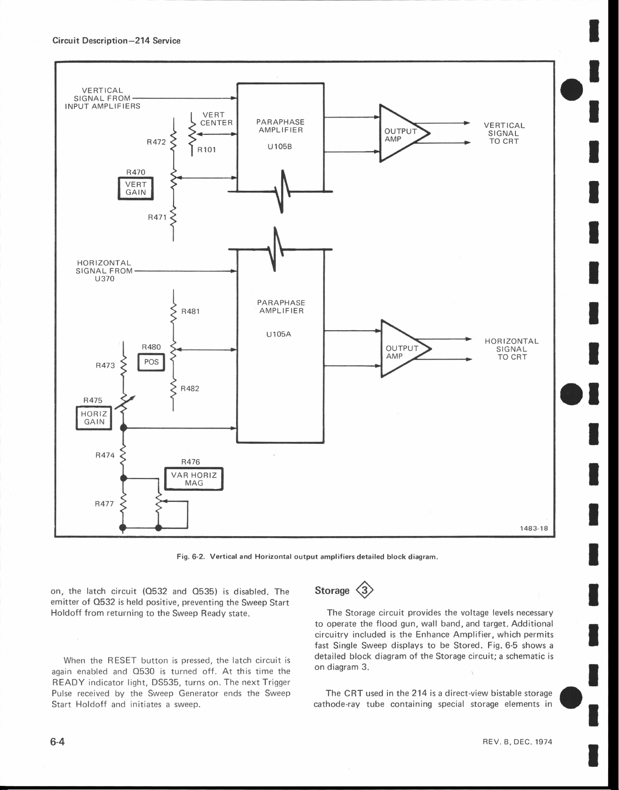
Ci rcu it Descriptio
n-214 Service
VERTICAL
SIGNAL
O"''''"J
INPUT
HOR
SIGNAL
FROM
IZONTAL
FROM
u370
-
R480
tril
VERT
CENTE
R 101
PARAPHASE
IF IER
AMPL
1O5B
U
PARAPHASE
IF
AMPL
IER
U1O5A
VERTICAL
SIGNAL
TO
CRT
IZONTAL
HOR
SIGNAL
TO CRT
o:
I
I
I
I
I
I
R475
r-l
rz_
I n(Jri
I r'l^ ll\l I
l
the latch
on,
emitter
Holdoff
When
enabled
again
READY indicator light,
Pulse
received by the
Holdoff
Start
I
e^rrv
I
R474
circuit
of 0532 is held
from
returning
RESET
the
0530
and
initiates a sweep.
and
R476
l*ilff"I
Fig. 6-2. Vertical and Horizontal output
(0532
button is
and 0535) is
positive,
to the
DS535,
Svueep Generator
preventing
Sweep
pressed,
is turned off.
turns on.
disabled.
the
Sweep Start
Ready state.
latch
the
At
this time
next Trigger
The
ends
circuit
the
The
is
the
Sweep
1483-18
amplifiers detailed
storase
to operate the
circuitry included
fast
detailed block diagram of the Storage circuit; a schematic is
on diagram 3.
The
cathode-ray tube containing special storage
Q
The
Storage
Single Sweep
CRT
block
diagram.
provides
circuit
gun,
flood
is
displays to
used in the214
wall band,
Enhance Amplifier, which
the
voltage levels
the
and target. Additional
be
Stored.
is a direct-view bistable
necessary
Fig.6-5
elements in
permits
shows a
storage
ol
I
I
I
I
I
I
I
or
6-4
REV.
DEC. 1974
B,
I
Page 43
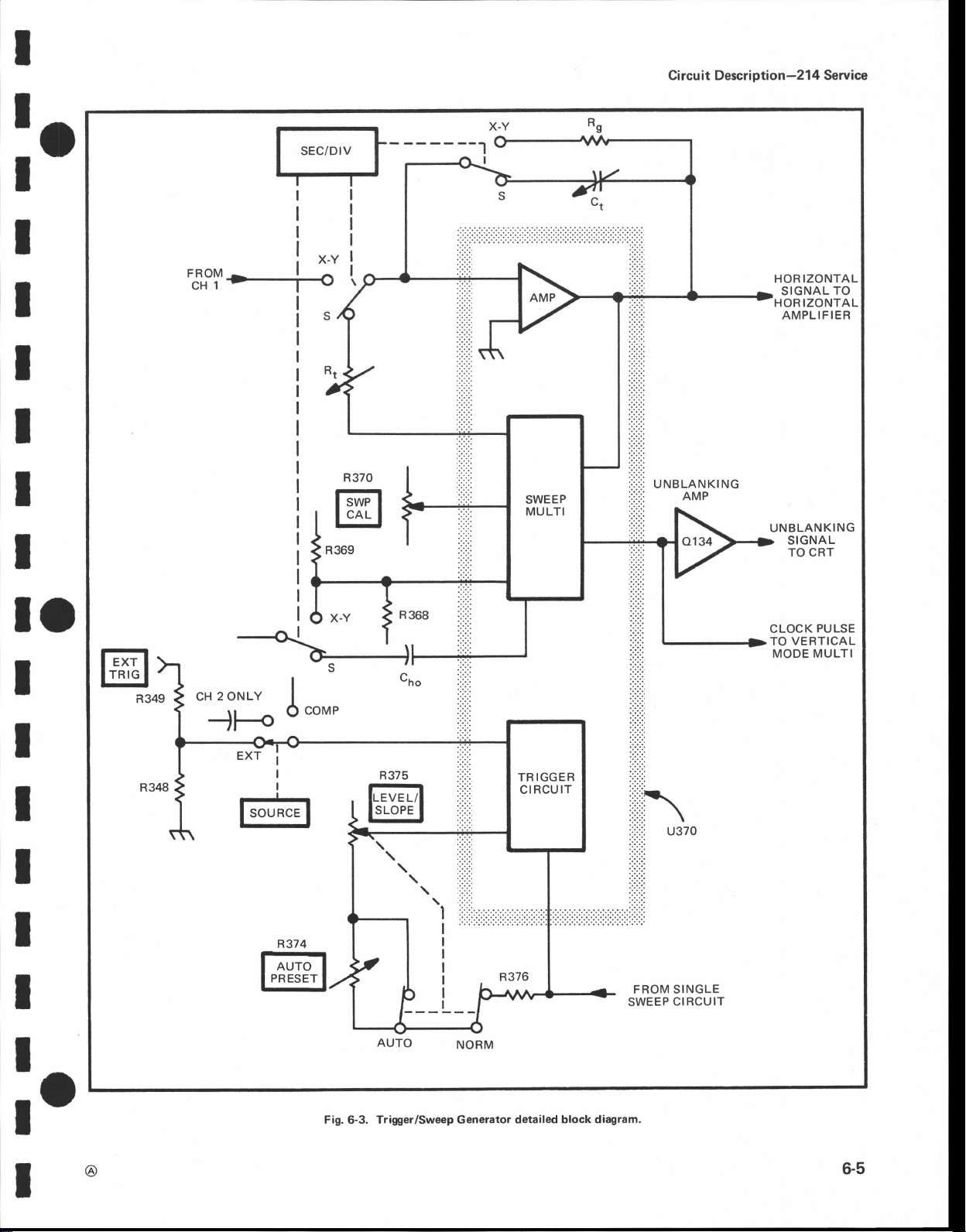
I
-o
I
I
I
I
I
t
I
tf""y+-i-o
',,
Ci
it Descri
rcu
UNBLANKING
AMP
ptio
n-214 Service
HORIZONTAL
SIGNAL
HORIZONTAL
AMPLIFIER
UNBLANKlNG
SIGNAL
CRT
TO
TO
lo
I
I
I
I
I
I
I
{2.NLY
2
ONLY
CH
Jl<
I
oco'tP
R375
@
FROM SINGLE
CIRCUIT
SWEEP
CLOCK
TO
PULSE
VERTICAL
MODE MULTI
lo
I
@
Fig. 6-3.
Trigger/Sweep Generator
detailed block diagram.
6-5
Page 44

it
Circu
Descriptio n-214 Service
F_sTffi"'Jf'-l
o:
I
I
I
I
Fig.
addition
operating
voltages
condition
operates
bombarded
bombarded
written display.
target operates in the conventional,
Power is
gun,
and
pushed
when
the
CRT
modes
R275.
The wall
electrons
effect
voltage
through 0505.
set by
Control
the conventional
to
mode
applied to these
of applied
in the
with
portion
With a different
applied
the
Storage
in. This reduces
in
the
NONSTORE
sensitivity between
are compensated
band serves
uniformly
on the
Amplifier
bombarding energy
level
of the wall
The
Operational Level control
ldentification
6-4.
of the tube
energy
-100
the
circuit
power
the
mode
for
as a lens
the storage
band
0512).
storage
only with the
by
potentials.
ready-to-write
high
shifts to the
by
over
ready-to-write
(O510,
writing
depends
the
state; then, when
writing beam
STORED
set
volt
drain
of operation. Differences in
STORE and
the
to distribute
is determined
potential
portions
of
gun
primarily
electrodes.
Storage screen
applied voltages,
of
NONSTORE, mode.
supply to
from
Store
target.
of the electrons.
R510 in
the
of
Sweep
elements.
on
With
(target)
current,
mode
to store a
flood
the
STORE
of the target
button
batteries
the
NONSTORE
Gain control,
flood
the
has
and
by
R506
the Target
The
the
one
it is
the
the
gun
no
The
SINGLE SWEEP
HOLDOFF
Holdoff waveform at Pin 5 of
Start
Storage
pressing
makes contact, a
applied
Control
target
entire
When the ERASE
pulse
band,
potential.
returned
Enhance
the
Store, Single
rates
Amplifier
the
Single Sweep
extinguished.
from
is
positive pulse
a
band circuits. The amplitude of this
determined by the
Erase. Erase of
releasing the ERASE
and
to the
voltage
target with
(about
pulling
0.1
of
the
target and
& Wall Board
above
-155V)
the target voltage below the ready-to-write
Then
the ready-to-write state.
to
Amplifier. Automated Enhance
millisecond/division and above. The Enhance
(0520
With
SEC/DlV
to
the
positive€oing
the
gun
flood
button is released,
is applied
the target and
Sweep
and 0521)
Reset
power
switch, the
the
Target Control
Enhance Level control,
_
Single Sweep
a Stored
wall band
Amplifiers. This
writing
electrons.
Mode of operation and
receives
circuit when the
applied to the Enhance
Enhance
Board.
display is
button.
pulse
through the
threshold
to
the target and wall
wall
band
a negative
achieved by
As
(about
pulse
and
a negativegoing
are
occurs
READY
Amplifier
Amplifier
Enhance
R526. This
the
switch
+155V)
Target
raises
writes
gradually
only in
sweep
at
pulse
from
light is
Amplifier
produces
wall
and
pulse
ol
is
the
the
is
or
I
I
I
I
I
I
I
I
I
6-6
@
I
Page 45

I
Circu it Descri
ptio
n
-21
4
Service
:o
I
I
I
I
I
I
I
FROM
SWITCH
FROM
LIGHT
SEC/DIV
READY
ENHANCE
AMPLIFIER
ENHANCE
LEVEL
--@
TL
+65
V
!-
55lOA
i"-* ät t äolJ
OPERATION
LEVE L
*-o t o-r,n-t,
Ft
I*-
I
WALL
BAND
F LOOD
GUN
HEATER
lo
I
I
I
I
Enhance
current is
I
I
-o
I
STORED
operate this
and connected
of this circuit is on diagram 4.
Power
Fig. 6-6
Supply
The
pulse
conditions the
required
state.
Power
shows
Supply
instrument
to an AC line,
a detailed block
Fig.
6-5. Storage
target
so that
to shift the written section to
less
O
provides
if
or,
the instrument is turned
power
the
recharge
to
of this circuit. A
necessary
the
writing
batteries.
schematic
circuit
gun
the
to
off
jP-'
55lOB
detailed block diagram.
the
When
power
AC
The
recharge
filter capacitor
operation.
of
power
The
DS310,
voltage or adequately
minutes of operating time
a
to
level of the
is capacitively
rectified DC
the internal
line. operating
POWER
is
illuminated
point
where
b-l
CURRENT
instrument
used to
is
for
the lnput
When
(BATTERY)
DS310
batteries
nzzs
".fto^,
GAIN
I
T
REFERENCE
batteries. The
the
when the
TO
155
R
is connected to
coupled to the
either
Rectifier
instrument
power
charged
falls
provided
is
indicator,
214
batteries.
remains, the
extinguish. When
will
below about
1483-20
power
a
Power Rectifier.
run
instrument or to
the
batteries act as a
in the AC
is not connected to a
by the
light
is operating
When about
battery charge
+10
line
line
batteries.
emitting diode
from line
charge
the
volts,
the
large
mode
five
drops
the
I
B, DEC. 1974
REV.
6-7
Page 46
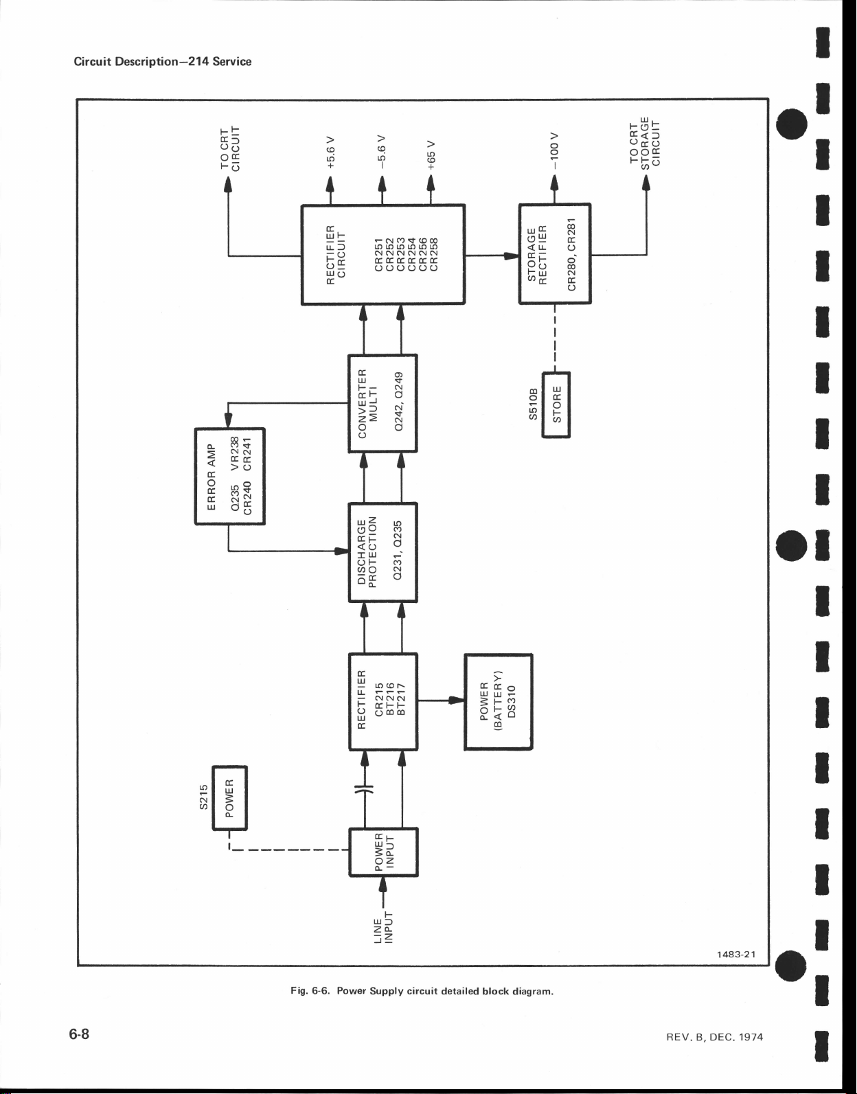
Circu
it Descri
ptio
n
-21
4
Servi ce
o
CE
o
CE
cc
uJ
rL
Er
()6
oE
FO
0Oe
(9t
C\N
(EE
>O
.^o
E{
11 c.l
;'icc
-()
uJ,
qeä
roqrö
+t+
(r
tuL
r.lf
-.\
tn trrrtrrrtrtr
Q=
ur
{E
FNc")\ttoo
rornlolo|'oro
(\lN$l(\lC!N
()()O(J()O
c)
cE
IJJ +
F-
at
2=$
oo
O
o,
(\
o
o
o
I
üü
<t!
öE
äH
I
I
I
I
,ff|
(r
ol
-I a I
;Ät v t
.l:l
$
o
I
ü
I
E3=
VE()
ootr
*
b.-,
o:
I
I
I
I
I
st
I
6s
c
E8
rJJ
f
Fc"l
l--
!
P8
c
CL
ol
t;I
frl ä I
r#
t_
___
Fig.
6-6.
E
tll
ll.
-
t:
H
TE
Power
.o(oF
FFF
c\Nol
(rFI-<-loo
(rp
-!
Lu
=d
oz
o--
F
ut
=,
zo-
=z
Supply
circuit
detailed
t
d:[ro
lll
e
UJ
<FC')
^j-u)
tsko
dl
block diagram.
I
I
I
I
I
I
1483-21
o:
6-8
REV.
B, DEC. 1974
I
Page 47
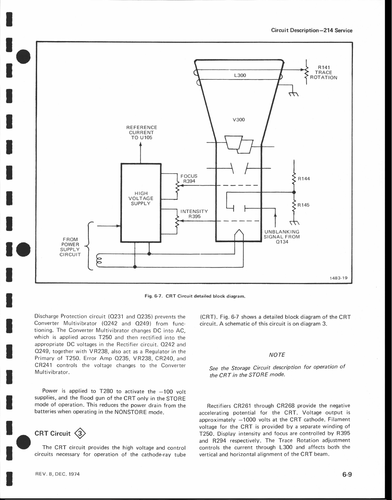
I
Circu
i t Descri
ptio
n
-21
4 Service
:o
I
I
I
I
I
I
I
lo
F ROM
POWER
SUPPLY
CIRCUIT
REFER ENCE
CURRENT
TO U105
IGH
H
VOLTAGE
SUPPLY
FOCUS
R394
UNBLANKING
SIGNAL
FBOM
o134
R141
TRACE
ROTATION
I
I
I
I
I
I
I
I
Discharge Protection
Converter
tioning. The
which is
appropriate DC voltages in
4249,
Primary
CR241
Multivibrator.
Power
supplies,
mode
batteries
CRT
.-.
V
The
circuits
Multivibrator
applied
together
of T250.
controls
is
and
of operation.
when
Circuit
CRT circuit
necessary for
circuit
Converter
across
VR238,
with
Error
the
applied
the
to
flood
This reduces
operating
g
provides
Fig.
(O231
(0242
Multivibrator
T25O
the Rectifier circuit. 4242
Amp
voltage
T280
gun
of the
in the
operation
and 0235)
0249l'
and
changes
and
also
0235, VR238,
changes
to
the
NONSTORE
the high
of
rectified
then
act
as a
to
activate the
CRT only in
power
voltage
the cathode-ray
Regulator
6-7. CRT Circuit detailed
prevents
from func-
DC
CR240,
the
the
drain from
mode.
and control
the
into
AC,
into
the
and
in the
and
Converter
-100
volt
STORE
the
tube
block
diagram.
(CRT).
circuit. A schematic
accelerating
approximately
voltage
T25O.
and R294
controls
vertical and
Fig.
6-7 shows a detailed
Storage
the
See
in the
CRT
the
Rectifiers CR261
potential
for
the CRT
Display
respectively.
current
the
horizontal
-1000
intensity
this circuit is
of
NOTE
Circuit
STORE
description
mode.
through CR268
for
the
volts at the CRT
provided
is
focus
and
Trace Rotation
The
through L300
alignment of
block
diagram of
diagram
on
for operation
provide
Voltage
CRT.
cathode.
by a separate
controlled
are
and affects
the CRT
beam.
1483-19
the
CRT
3.
of
negative
the
output
Filament
winding of
by
R395
adjustment
both the
is
I
REV,
B,
DEC.
1974
Page 48

o:
I
I
I
I
I
I
tl
I
I
I
I
I
I
o:
Page 49

cA2
PROBE
>4
(cH
2)
tffit
ATTENUATOR
-19!.31-
*ry
cH2
INPUT
o3l4r
ua?o
IRI66ER
ICKOFF
P
ae26, oazs
cHz
VERTICAI
2{9
€
SWllcH
U32OA
AAp
CHAN
lffi;l
-
I
ALT
CItOP.
CLOCK
oaaot o36a
UNBLANKIN6
AlilPLl F
a3t2,ota4
IER
ENHANCE
Ar{PLIFIER
o520
092l
HORIZONTAL
AMPLI
FI ER
U IOSA
l9
ol
ol22
BAND
AMPLI FIER
o50'
FLOOD 6U[
ANO9E
iEi
?
ol
^i
:O.
'D
:
>:
31
cHl
PROBE
2t4
(cH
tml
t)
(cH
t)
lvoLTs/DlVl
POWER
9U
PP LY
a?i,t , a7)6
a242,
O249
R,EV
POWER
ALL
-toov
SAORA6E
APR
TO
CIRCUITS
To
I98I
BLOCK DIAGRA/V\
Page 50

$g
5a
rs
!t
3E
-o
Eg
o
.n
E
U
U
oUo
:
E
o
E
I
o
;
o
;
D
z
q
ocooo
t
o
o
o
F
!i
Page 51

214
Service
The voltages and waveforms
obtained by using the following
equipment.
Voltage Measurements:
Set the
Input coupling
tioned to
Voltmeter
common.
front
and side
switches
the center horizontal
common
shown
panel
controls
ground
to
line.
is connected
VOLTAGES
on this diagram were
test
set-ups and test
to mid-range.
(GND).
to
the instrument
RECOMMENDED
Trace
posi-
AND WAVEFORMS
Waveform Measurements:
The 214
panel
switches are set
with a two millivolt sguare wave
two millivolt
switch is
Test
triggered; the vertical deflection
indicated
coupled. The
2Oo/".
The test oscilloscope used for
Tektronix
TEST EOUIPMENT
Oscilloscope
controls
are set to mid-range.
to AC. The vertical
sine wave
for 0.5 m
set
Oscilloscope: The test
on the waveform
tolerance
7503 with a readout
under
test:
connected
connected
with
a trjggered
oscilloscope
and horizontal
photo.
of the voltages
The vertical
display.
The
The input
deflection
to
CH 2.
display.
and
the
wave forms
front
and
coupling
is
set
to 1 m
to
CH I and
The
SEC/DIV
is internally
timing
input
is
waveforms
was
side
a
is
AC
is
a
Oscilloscope
Voltmeter
multimeter
nonloading d igital
ITEM
SPECIFICATIONS
Frequency response 500 kilohertz. Tektronix 2'11
lnput impedance:
Range:0-l
10 MSI
kV
RECOMMENDED
Tektronix 7D1
test oscilloscope
required.
Fairchild Model 7050
TYPE
equivalent.
or
3 Digital multimeter,
with
readout
equivalent.
or
is
Page 52

o
z
etr
.+
ge
ß
a
F
?
F
)o
i
i
':
:f
s<
.X
st ;
----{ 9I
r3+
ts'1-.1 .l- 4
t3ä
oö
ö
d'
,z\
ig
tE
ir
F9
22
go
,f
rP
tö
-r(ö-
J
iF
;l
t-
ig
!*
it
ül
l-o!i
fl3:
"lsc
rS
g8
\
!t,n
^Eg
rFi
Iee
f_
gz
NS
!o!
i:t<
5<9
f
äüfr
lvctIu3A
000O0lA
ä
dn
|.rdyrtv
J
ä;ti
,1
vru3|
sH
*{
z!
rä
sä
'>
;3
83
ro
eäs
.i\
:F
5i
3'
bf rr
0;
i6
9o;
lsÄ
oöi
'*$
E$-
eiPP
t>;'r
f
3
F
i
P
et-d%{_rtFrb-$
A
,
2
c
i
R
z
a
t
,
o
p
rn
-
r-
!
ilJ: *l
a.
r
.,ri:.i
lmn
ii.:l'i
'rÄ'{
ilsg::
r
1#uii
fii?,.Il
Hüili
c0r's
Iqadl
o
rFil
zqo
T
m ütö
üat
a
Si
Page 53

st{o[.v301
uf
lt{3Nodnoc
Ht'ldul zv
i:r1,y'i'9"r1"tilrt,
^ll
hD:ltl.
I rXrRoillx.
Rrstt vM
l,
äfi8
=H;
iär
äs
Eg
Page 54

t
+
aI
6r
U
0r
_l3l!H3
-@
eeeo
'o16,
)
I
I
I
/i.
I
loüD
Nt x:ao
t4ä*
M!
rol
;E;-Tfr-T;
--jJ-Y
(Ba) olE
"t
//
ov,Äl
,/,
'
|t:'
I
I
/:
4r'9.
,
I
ee?J
|
!'t.9
|
lE*) t
"Ar+
|
F"l /
tl
lqt-;r
I
tr'r
ll
rl
tl
T-t
d
^r.l-_,n
n"L* 1l#,
(lldro,
^l
sl
c\
sl
r
orea{
5r€:
(rraro)
(lrd)d)
o*
i
I
I
I
I
I
I
I
i
i
I
ll
,r,s-
-l
(r1il)
6Z6a
I
9ZA
I
n"l
,
629!
-i'r
iel
I
(rd)c)
I
I
0t5
" ' i:'J.', ,i il-,'r -.- .
y/vurvfv
|
'f
ot
otg
or
l,
t-r
I
,
9Er zrc
9rs 9r!l
*es
bo
gorn
Itgg 0r
>6
uu
E9
-
(ö
-
ö
iG
<o
dE
Et
u
G
o
ttL
1tuNrl
hl
tHt
r
oxooJ
l0Nrrdo@
r-:gEi-
l,'
l"
ir
t:
1."
F.
drlelH
tNvr€r9al+
sttd
?otlt
YIoMEN
\
trt
4;:H"^i..
lztd
tvtttvd
(r1d.o)
!liltv:
5:1i-iKtllJ tv'iiJf
üJfll;!i'ril:
lztd
owo€ lndxt
-lvf,lläfA
lv
O
ällJlldldv
ooooorsNs n"rae
I
:.EJ
(radX)
tNc
-l^rciffiil-
u3)
zrloB
(
'
.l
t c'l
9'
ä
Alw
Afl
os6t
s-i.?Y,:t fis
{lNY
i'J al:il!8
g::ilallo3(
!a:!r.!;f
Sl.:lV(
;:H5 Ni
3:n]v^
Ac
Page 55

sNollvco'l INSNodti\to3
rndNt
00000rs
'lvcrl-u3A
NsMo]38
tv
Yo
.,
; oi
/f.
ft.**,;*;r$
r
qEo
! -6
5Ez
--
z3ö
ögB
- h:
d6i .€
d!
gE
q
3gP
J.
ä
g
$:
I
:
.$lgdr
:"t
-f'.?Tl:{fr
Flil-*ry4;ij
"
lft$m;
.'lä',
.*i&F"r
1..1.:3J
",
'E
I
r"
*1
i.
]rh
üG
*
*
:.'l
_q
ö
o
c
e
U
u
u
E
o
u
{ä'
ii,
'IE
,f1"rcäL.il.
iTh"#
ä
oo-?g#
r
6'
,ü-
\\
\
Page 56

214
Service
The
voltages
obtained
equipment.
Voltage
tioned to
common.
Measurements:
Set the front
Input
coupling
Voltmeter
and waveforms
by
using
and
sruitches
the center
common
the following
panel
side
horizontal
controls
ground (GND).
to
line.
is conngcted
shown
test
VOLTAGES
on
this
diagram
set-ups
to
mid_range.
to
R ECOMMENDED
and
posi-
Trace
the. instrument
AND
were
test
WAVEFORMS
Waveform
The 214
panel
controls
suritches
with
a two
two
millivolt
switch
is
Test
triggered;
indicated
coupled.
2OoÄ.
The
Tektronix
TEST EOU
IPM
Measurements:
Oscilloscope
are set
are
set
to
AC.
millivolt
set for
Oscilloscope:
the
on
the waveform
The
test
7503
ENT
square
sine
wave
0.5 m with
vertical
tolerance
oscilloscope
with
a
under
to
mid-range.
The vertical
wave
connectd
a triggered
The
test
deflection
photo.
of
the voltages
used
readout
display.
test:
The
front
The
input
deflection
connected
to
oscilloscope
and
The
for
the
to
cH 2.
The
display.
horizontal
vertical
and waveforms
wave
and
coupling
is
set
CH
1 and
SEC/DlV
is
internally
timing
input
forms
to
is
was
side
1 m
a
is
AC
is
a
Oscilloscope
Voltmeter
multimeter
nonloading
ITEM
d igital
SPECIFICATIONS
Frequency
Input
impedance:
Range:0-1
response
10
kV
500 kilohertz.
MO
RECOMMENDED
Tektronix
Tektronix
test oscilloscope
required.
Fairchild
211
or equivalent.
7D1
3 Digital
Model
7050
TYPE
multimeter,
with
readout
or equivalent.
is
Page 57

F&h
orreQ
so
I
T'
LJ
l-"
l"o
l'o
l.
I
Ti
l"
Ll
[*
lb
rlo
L,
.c$2
t4
BCF
ttstD
st
R!6tC
t@k
PlatS
9k
i4::;s
A\J :::.
HAI+üiS fcDri-'l
jFi.(;:cirj
HORIZ
CINTER
..:
tL.tuni;.
-' .c:rll
j
,
ti
lffil-Y38
vlmru
Fg
"izi
H'l
t
'
| |
+2_2v cENitR
| |
|
|
| ,/
ß'3,1Fi
r
(DC?!1)
ll
---:il:i:
i'i"
vGtr
+VERT
5tO
TO PrNtO, ffi
Draog
-vEg
stc
TO
PtN ||,
cRT
Dlaq
(g
e
QEzO
oeo
p
c570
orrcQ
J#"
tElltBi-el ts
IGßl
ta19
,
cdPosEE
FsM e$2
H.",Tf.i'io+
>i]
t@
_ ::i
Ttro
sk
ffiBr-öfiH
atö
O
EXI
as79
t'-El
-agvswt@
N ruIL
REV
rw!l/sLoE
H
oPrN
CCW
DEC
OF
t'AO
PART OF ETCHED
*
PARAIAL
NOTE: FOR
see
R482
6t
!nl
(06p!,
\ilßrN(
TO
CIrcUIT BOARD
AI,INPUT BARD
qOMPONENT
Fr6.9-r FOe
At
LOCATIONS
BOARO.
HoR.tz{veer
-5.N
(ocEl)
I
f8l'f
I I
oerz)
| |
L--=l
| |
Raqro;
i
_Jl
Rt32
&37
rk
ii:ti
mTl^l
Aa, A$PLIF|ERaOARO
ouTpurs,TRIGGER
swrre
i
+
9t6
H4tZ
TO
PtN Cr CRT
orre@
-
916
aoRtz
TO PIN
9, CRT
oreg
fil-
!S--.*o'
i.r
lIh\
)+ORRAI
ELTs
FOPMERLY
PZr,
SIGXAL rc
Prf,
Draqo
c*wx"
PrN
I
UNALA{KIN6
q,
cRT
DtaqO
"rro
@
po
ON
:::
F
zm
=t
2p
sf
g!
Page 58

&
L(rcATIONS
Sil!'EEP
SUPPLV
5
@oo
@il!
=t=
*'5
sa
F=
Hts}
d
.l
F'-l-"'
ofr
ä4
a3 Po,uEd
A/t SINGLE
COMPOIIIENT
gls
Eli
rä
ä
I
!
rtt
!
D
F
o
@
r
0
l!
F)
I
P
?
mmm
@
Page 59

H
l!
(o
I
5
(t
t
o
v,
{
t
I
aa
tr
o
o
F
!
D
@q,G'
@
I
Page 60

VOLTAGES AND WAVEFORMS
214
Service
The voltages
obtained
by using
equipment.
Voltage
Measurements:
Set the
front
Input coupling
tioned to
the center
Voltmeter
common.
Oscilloscope
Voltmeter
multimeter
and waveforms
the following
side
panel
and
switches
horizontal
common
nonloading
is
digital
shown
on
test
controls
ground
to
line.
connected
this
diagram
set-ups
and
were
test
Wavef
The 214
panel
switches are
with
two millivolt
to mid-range.
(GND).
Trace
posi-
switch
Test Oscilloscope:
triggered;
indicated
coupled.
to
the instrument
2oo/o.
Tektronix 7503
RECOMMENDED
TEST EOUIPMENT
SPECIFICATIONS
Frequency response 500 kilohertz.
Input impedance:
10 MO
Range:0-l kV
orm Measurements :
Oscilloscope
controls
a two millivolt
are set
set to
AC. The vertical
square
to
sine wave connected
for
is set
0.5 m
with
The
the vertical
deflection
on the waveform
The tolerance of
The test oscilloscope
with a readout
RECOMMENDED
Tektronix
Tektronix
test
oscilloscope
required.
under
test:
The front
mid-range.
The
deflection
wave
connected
to
CH 2.
a triggered
test
display.
oscilloscope
and horizontal
photo.
The vertical
the voltages
used for
the wave
display.
211 or equivalent.
7D1
3 Digital multimeter,
with
input
is
to
CH
The
is internally
input
and
waveforms
forms
TYPE
readout
and
side
coupling
set to
1 m
1 and
SEC/DlV
timing is
is
AC
was
is
a
is
a
Fairchild
{:r
F
.1
;
ä
t'l fiö
'.
r,q'9
?9 * I I i,
.-.
f,.i'l
.i:I
\r
--*---ii-*
+i*
!;-J
.f:,t.,.l
'
't..':r
ir;
!,'
:
1ä
"^
€-
..ea-..
..i.-
''{t'
'.1
r
',
:i
'.
.1 .'
r
r,e;
i
6r'
,1.
'|
i.:1'7
.;
l
...-"..r.i....
*-
i:,
I
-
:--
r.-
1
.J'
1.'
i
"€..i
':.l,j;.::
,:i.!.;ii-
,..i
l
.',.t,*,
iill
ti;
ij;{.
'1,
'',
'+
far;
i..f'
"1.
i i._
{- erlrV
i
ltrl
a';'
r:i'i
.i
!15
i
I
,,-,
1,.
l;'
,:
l,
'1"-.
,.".
,i.-
.l-- .-''
-
,-,it'-i: r
...\,,
r.
,
,,.'i
.j-r
:
l
i
.
,.i!. ,"1.t"
;
.'-:'
i:.lt'iij:!,'r)1.!a.
;i:','!.I
rs
, : +ts
tflF
. .
x-"1.,,,,. ,.,.,."*
: l
t,.
.l'
':t'j
i
.
r' i
1
"'
'
,,.i-*
t#'-*
.
':
|
::.,
i
:
l.
:
i
i:
:
t
'.1,.;
i:i:"'
|,...,!tt.-
r-i
i
I
i /..-.,,.1
{:,:.
i'
;
.:-".,,i'
li"?r'l
i
:
!
:
i
l,
{
Model
i
k'
'..',;.
7050
equivalent.
or
i
I
I
Page 61
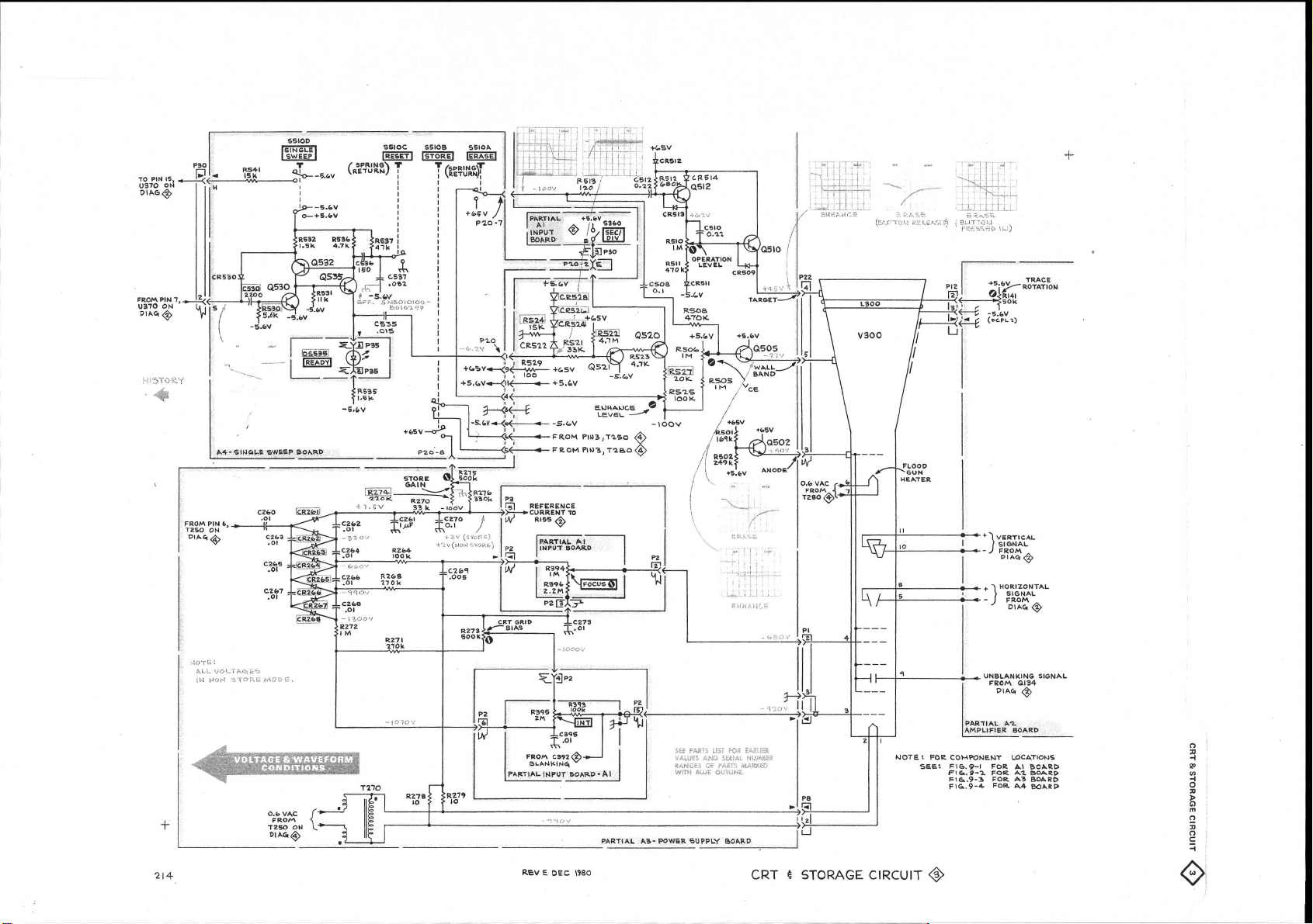
gSi
'a
Ädt
"l#;ij
*.
o9:
ffic
I
l^
I
I
,i;
*Ft
I
ePr
t
t9
i
a
+
!t
o
o
!ü
i\
i$r.
o
l,r
i3
"?e
$Hl
ül
'F;l
**
o
o
s*s I
t{ |
tl
^=
oA
oY{
I
ol
+|
sl
?*
XXt^
9ie
!f
ul
hc
f;i
i
"'
r{
TC
ö
P
Fir
!g
to
"",
Ä.ö \*
o6
6$
I
+l
cl
I
ö
I
I
It
I'
t$
lLt
__)\
Ilil
*Fi+
üii-71
l
flqT
'81
t
i
-\
-.o ;i
!\1
-fri
t-:u
XP
0
,
;ggi
0'i
YY
:äöi
yi?
\zt
ö
c
r
tli:
N
oi
6!ii
niln
\z
eBP
r3t
a>
otJ
Z
{
o
m
p
o
!
I
?
äT-":i
i, *d
ilirü
r__-___l
tr8U
n-
Tö
arllr
rir-?
pur_
e99o
f;
ntnn Z
ooOo
al,0D
L
;ts
l!t<t>
0
o
lrIt>
l0
l3
la
ld
lFrqt!
Il@lo
t,
l"
I
I
I
L_.
'|
o
-{
(t!
--l
m
o
o
o
nnc
f
o
oE;
,
ir
>>>> 5
6
z
I
o ort
rnFp;
9990'
9eB9
r
a ruc
ruvuors
.,n"r,"
Q
Page 62

214
Sewice
The voltages
obtained
equipment.
Voltage
tioned
common.
Measurements:
Set the
Input
to the center horizontal
Voltmeter
and waveforms
by using
front
and side
coupling
common
following
the
panel
wvitches
is connected
shown
on this diagram
test
controls
ground (GND).
to
line.
to mid-range.
to the instrument
VOLTAGES AND
were
set-ups
and test
Trace
posi-
WAVEFORMS
Waveform
panel
switches
with
two
switch
triggered;
indicated
coupled.
2O%.
Tektronix 7503
B ECOMMENDED TEST
Measurements
The 214
a two millivolt
millivolt
Test
The
Oscilloscope under
controls
are set
sine
is set for
Oscilloscope:
the
on the waveform
The tolerance
test oscilloscope
EOU IPMENT
:
are set
to AC.
0.5 m
vertical
with
to mid-range.
The vertical
square wave
wave connected
with
a triggered
The
deflection
of the voltages
a readout
test: The front
deflection
connected
to CH 2.
test
os€illoscope
and horizontal
photo.
The
used for
display.
The input
to
display.
vertical
and
the
wave forms
and side
coupling
is
set to 1 m
CH 1 and
The
SEC/DlV
is
internally
timing is
input
is
waveforms
was
a
AC
is
a
ITEM
Oscilloscope
Voltmeter nonloading
multimeter
digital
SPECIFICATIONS
Frequency response
impedance:
Input
Range:0-1 kV
10
500
MO
kilohertz.
RECOMMENDED
Tektronix
Tektronix
test
required.
Fairchild
211 or equivalent.
7D1
oscilloscope with
Model 7050
TYPE
3
Digital multimeter,
readout
equivalent.
or
is
Page 63

atrüL at-
ll{PuT 90aF,0
rrlrrilii'rl
-
,rlJlllll,ljl
o,.u
I
AOCRT
I
/
Dra6O
. loc2@
Dras
o.
HEATER
O
o
E
n
t
@
c
!
!
?
o
F V,)r.:fl..iE
rF*3eLEctED
VöLTAGE TANG€I
P.i:6 1 . !1t
FoE
NOE:
jgg
dri;:iJ
t;N:ES {:t
!; b(:l{TfD iN Bl:,18.
t,
Lrus
FOR COMrcNENT
gEE1
Flq,9-t FOR
FIG.9-2
FIq.
FIq,9.4 FOß
r_i3
:rr.*an
i;3t;i: ritr!:i€f:
*S1
pA€T€
:iit
'-3 FOR A:
r i.!:q cr.äi.i[]11
llj;i;:lti:.
,ö
rl
F+65v
tl
tl
tl
tl
tl
tl
il
!j-*
l'l
F-sev
0
+.ov
--..:,,.,
aßi,i
@?ft
JCL56
!
czEe
'
6.aaF
?'"??ii,",
1
I
E;
lEl
)*
llL
IW
IB
lFt
o,a40
oreeQ
FOR
aO.O-,Oat
At eoARD
A2
RoARD
bARD
A4
BOARD
I
I
PARThL
A3-PowERsuPPtY
Bl?llg
REV G SEP I97<I
POWER
SUPPLY
O
Page 64

I
REPLACEABLE
Section
8-214 Service
:o
I
I
I
I
I
I
I
lo
ELECTRICAL
PARTS
Replacement
or representative.
Changes
components as they become
improvements
ordering
type or number, serial
Tektronix, Inc. Field Off
number.
parts,
part you
lf a
Change
parts
to Tektronix
developed
include the following
to
have ordered
information,
available
are
instruments are sometimes
in
number,
ice
or
if any,
SPECIAL
X000
00X
ORDERING
from
orthrough
available,
our engineering
and modification
has been replaced
representative
and
information
will contact
is located at
NOTES
first
Part
Part
added
removed after
PARTS
INFORMATION
your
localTektronix,
made to
you
give
to
department.
your
in
number if applicable.
with a
you
rear
the
AND
of
SYMBOLS
this serial
at
this serial
accommodate
the benefit of
lt is therefore
Part number,
order:
lmproved
new or
concerning
this manual.
number
number
Field
lnc.
improved
the latest
important,
instrument
your
part,
any change
Office
circuit
when
local
part
in
I
I
I
I
I
I
Parts List, an
ln the
Because of space
further ltem Name
utilized
ACTR
ASSY ASSEMBLY
CAP
CER CERAMIC
CKT
COMP COMPOSITION
CONN
ELCTLT
ELEC- ELECTR]CAL
INCAND
LED LIGHT
NONWIR NON
possible.
where
ACTUATOR
CAPACITOR
CIRCUIT
CONNECTOR
ELECTROLYTIC
INCANDESCENT
ltem
limitations, an
identification,
EMITT{NG DIODE
WIREWOUND
ITEM NAME
Name is separated
Name
ltem
the U.S.
from the description
may sometimes
Cataloging
Federal
ABBREVIATIONS
PLSTC
QTZ
RECP
RES
RF
SEL
SEMICOND
SENS
VAR
WW
XFMB
XTAL
by a colon
incomplete.
as
appear
Handbook
PLASTIC
QUARTZ
RECEPTACLE
RESISTOR
RADIO
SELECTED
SEMICONDUCTOR
SENSITIVE
VARIABLE
WIREWOUND
TRANSFORMER
CRYSTAL
H6-1
FREQUENCY
can
(:).
For
be
!.
@
I
8-1
Page 65

Replaceable
Eleclrlcal
Parts-2l4
Servlce
I
Mfr.
01121
0l 295
03508
03888
04713
07263
1t237
r4433
r4752
1
6546
270L4
32997
5t642
56289
7 1450
72982
73138
7591 s
76493
79727
80009
8003
8441
90201
9r637
Code
I
I
Manufacturer
ALLEN-BRADLEY
TEXAS
INSTRI]MENTS,
GROUP
GENERAL
PRODUCTS
KDI
PYROFILM
MOTOROLA,
FAIRCHILD
FAIRCHILD
cTS
KEENE,
ITT
SEMICONDUCTORS
ELECTRO
U.
S.
CAPACITOR
ELECTRONICS
NATIONAL
BOURNS,
CENTRE
SPRACUE
cTs
ERrE
BECKMAN
LITTELFUSE,
BELL
MILLER,
C-I.l
TEKTRONIX,
ELECTRA-MIDLAND
TRI{
MALLORY
P.
DALE
ENGINEERING
coRP.
TECHNOLOGTCAL
INDUSTRIES,
INDUSTRIES
ELECTRONIC
R. MALLORY
ELECTRONICS,
COMPANY
ELECTRIC
DEPARTMENT
CORPORATION
rNC.,
SEMICONDUCTOR,
CAMERA
INC.
CUBE
INC.
DIV.
SEI'TICONDUCTOR
rNC.,
TRTMPOT
ELECTRIC
INSTRIJMENTS,
INC.
J. W.,
INC.
CAPACITOR
COMPONENTS,
AND
CROSS INDEX-MFR.
INC.,
SEMICONDUCTOR
COMPANY,
SEMICONDUCTOR
AND
CORP/CENTRALAB
INC.
CO.
PRODUCTS,
INC.,
DIV.
CORP.,
CO., DrV.
CO., rNC.
INC.
SEMI-CONDUCTOR
PROD. DIV.
A DIV.
INSTRTMENT
CORP.
PRODUCTS
INC.,
rNC.
HELIPOT
MEPCO DrV.
TRI.I CAPACITORS
OF
OF
CORP.
DrV.
DIV.
CODE NUMBER
TO
Address
12OI
2ND STREET
P
O BOX
EXPRESS}JAY
ELECTRONICS
60 S
5005 E MCDOI{ELL
464
3230 RIVERSIDE AVE.
3301 ELECTRONICS
P O BOX
17IO
4561
29OO
I2OO
2820 E
905 N. I{EST
644 W,
25OO HARBOR
8OO
19070
550 DAVISVTLLE
P
22
ll2
3029
P.
P. O.
5012, 13500 N CENTRAL
JEFFERSON ROAD
ELLIS STREET
S. DEL
coLoRADo
SEMICONDUCTOR DR.
COLUMBIA
E. NORTHI.IEST
O BOX
COLUMBIA ROAD
I.l. FIRST
E. I{ASIIINGTON
O. BOX
PARK
3049
MAR AVE.
COLLEGE AVENUE
BLVD
t2Trr ST.
BLVD.
REYES AVE., P O BOX
500 BEAVERTON,
372 TNDIANAPOLTS,
BOX 609
MANUFACTURER
SOUTII
RD,PO BOX
T{AY
AVE.
IIT{Y
RD.,p O BOX
ST.
STREET
20923
5825 COMPTON, CIL
96
State,
City,
MILI'IAUKEE
DALLAS, TX
SYRACUSE,
WHTPPANY,
PTIOENTX, AZ 85036
MOUNTAIN
PASO
ROBLES,
I{EST
PALI'I BEACII, FL
sAN GABRTEL,
LOS
ANGELES,
SANTA CLARA,
RMRSTDE,
STATE
COLLEGE, PA 16801
NORTH
ADAMS, t4A
ELKIIART,
ERIE, PA 16512
FULLERTON,
DES PLATNES,
I{ARMTNTSTER,
MORRISTOhIN,
OGALLALA, NE 69153
COLUIiBUS, IitE 68601
Zip
WL
53204
,
75222
NY 13201
NJ
07981
VIEhI, CA
CA 93446
CA 91776
CA 90039
CA 95051
CA
92507
CA
rL
90224
pA
OR
NJ
01247
92634
60016
18974
97077
07960
rN
rN 46514
o:
I
94042
I
33402
I
I
I
I
46206
ol
I
I
I
I
t
I
o:
8-2 REV
H, MAY
1980
I
Page 66

I
Replaceable
Electrlcal
Parte-214
Servlce
:o
I
I
I
I
I
t
I
lo
I
I
I
I
t
I
Ckt
AI
AI
AI
AI
A2
A3
A3
A3
A3
A4
A4
BT2l6
BT2t7
c10l
cl03
c104
cl04
cIl3
cll5
ct25
ct27
cI29
cl50
cl50
cl53
cl53
c204
c204
c206
c206
c207
c207
c2l0
c2l0
c2t0
czt2
c2t2
czt2
Tektronix
No,
Part
670-2353-01
670-2353-03
670-2353-05
670-2353-07
670-l
670-2741-OO
670-274t-Il
670-2741-21
670-274I-31
670-2676-00
670-2676-0r
146-0033-00
146-0033-00
283-01
283-0111-00
281-0591-00
283-0180-00
283-0lll-00
283-0111-00
290-0524-00
290-05?4-00
290-0522-00
281-0591-00
283-0180-00
281-0591-00
283-0180-00
283-0263-00
283-0279-00
283-0057-00
285-1065-00
283-0057-00
281-1065-00
285-0925-00
285-0933-00
28s-0935-00
285-0925-00
285-0933-00
285-0935-00
No.
505-02
ll-00
Serial/Model
Eff
B0l0l00
8055612
8090000
B100000
B010100
B050000
8010100
8060000
8010100
8066827
8010100
B066827
8010100
8,066827
B0l0l00
B051
100
8010100
B05t
100
No.
Dscont
805561 I
8089999
8099999
8049999
8059999
8066826
8066826
8066826
Bo5l099
8051099
Name
BOARD
CKT
CKT
CKT
CKT
CKT
CKT
CKT
CKT BOARD
(oprrou
CKT BOARD
(oprron
CKT
CKT
BATTERY
BATTERY
CAP.
CAP.,FXD,CER
CAP.,FXD,CER
CAP. , FXD,
CAP.,FXD,CER
CAP.
CAP.,
CAP.,
CAP.
CAP.,FXD,CER
CAP.,FXD,CER
CAP.,FXD,CER
CAP.,FXD,
CAP.,FXD,CER
(llourxll
FREQUENCY.
CAP.,FXD,CER
(nournel
FREQUENcv.
CAP., FXD,CER
CAP.
,
cAP.,
CAP.
,
CAP., FXD,PLSTC
(nournAl
FREQUENCY.
CAP.,
(r,tourua,l
FREQUENcv.
CAP.
,
(nournu
FREQUENCv.
CAP.,
(nournal
FREQUENCY.
CAP., FXD,
(nournel
FREQUENCY.
CAP.
,
(nournal
FREQUENCY.
ASSY:
BOARD
ASSY: INPUT
BOARD
ASSY:
BOARD
ASSY:
BOARD
ASSY:AMPLIFIER
BOARD
ASSY:
BOARD
ASSY:POtfER
ASSY: POI.IER
t
onl,y)
ASSY:POI{ER
2 oNLy)
BOARD
ASSY:SINGLE
BOARD
ASSY:SINGLE
ASSY:2
ASSY:2
FXD,
CER DI :0.
,
FXD,
,
FXD,
FXD,
FXD,
,
FXD,
FXD,CER
FXD,
FXD, PLSTC
FXD, PLSTC
FXD,PLSTC
FXD,
DI :0.
DI
CER DI :
DI
CER
DI :
ELCTLT
ELCTLT :
ELCTLT:
DI :
DI :
DI :
CER DI :
DI :
VALUE,
sEE
DI :0.
VALUE,
sEE
DI : 0. lUF,+80-2OZ,?OOV
PLSTC:
DI :
PLSTC :0.OIUF
VALUE,
SEE OPTTON
vALUE,
sEE opr
vALUE,
SEE OpT
vALUE,
sEE oprroN
PLSTC
VALUE,
SEE OpT
PLSTC
vALUE,
SEE
:
:4.4UF, I
& Description
INPUT
INPUT
INPUT
POI{ER
SUPPLY
SUPpLy
SUPPLY
SUPPLY
STTIEEP
SI{EEP
SETS
OF
SETS
: 5600PF,202,200V
5600PF
: 0. lUF,
0. IUF , 202
: 4.
4. 7UF,202,
lUF
5600PF,202,200V
5600PF,
5600PF,2OZ,?OOV
5600PF,
0.0022UF,
SELECTED FoR
oprroN
SELECTED
opr
0 .OIUF,
0. lUF,+80-2OZ,ZOOV
:
3. 3UF, 102,
SELECTED
: 2UF,
SELEcTED FoR
:4 . 4UF,
SELEcTED
: 3. 3UF,
SELEcTED
2UF,
SELECTED
SELEcTED
OpT
5
OF
5
IUF,
20U,
1UF,
7UF, 202,
,2OZ ,5OV
00lUF, 202,
l0Z,
102,400V
INFORMATION.
INFORI.TATION.
50V
202,50V
,207" ,200V
20Z,50V
,50V
l0V
l}V
2O"A,2OOV
2OZ,IOOV
202,
tnronuarron)
3000V
FoR
rNFoRMATroN.
20U,600V
,2O"A
,600V
200V
FoR
LrNE
TNFORMATTON)
400V
rNFoRMATroN.
I 0Z , 200V
INFORMATION.
l0Z,
02
LrNE
FoR
LrNE
200V
FoR
LrNE
rNFoRI.tATroN)
FoR
LrtfE
200V
,
FoR
LrNE
3000V
LrNE
LrNE
voLTAcE
voLTAcE
opr
I oNLy)
VoLTAGE
votrAcE
opr I
voLTAcE
OpT
2
voLTAGE
VoLTAGE
OpT
I
voLTAcE
OpT
2
oNLy)
Oltt
Ottty)
Oltty)
Mfr
Code
80009
80009
80009
80009
80009
80009
80009
80009
80009
80009
80009
80009
80009
72982 8l2l-N088Z5ULO4M
72982
72982
72982
72982
72982
90201
90201
56289
72982
72982
72982
72982
56289
AND
s6289
AND
56289
14752
56289
14752
844rr
AND
r4752
AND
56289
AND
y)
84411
AND
14752
AND
56289
AND
Mfr
670-2353-01
670-2353-03
670-2353-05
670-2353-07
670-1505-02
670-274t-OA
670-274L-tr
670-274t-21
670-274t-31
670-2676-00
670-2676-0I
146-0033-00
r46-0033-00
8t2l-N08825U104M
39300125v05622
8121N204
8121-N08825U104M
8l2l-N088Z5Ul04M
TDC475n0loEL
TDC475M0loEL
l96Dl05x0050nAl
39300125v05622
8121N204
39300125v05622
8121N204
33C319
55c153
274Ct0
230BlFl03
274Ct0
230BlFl03
TEKI2
A-1480
430P179
TEKl2l-33592
A-1480
430P179
Part
-33592
I
Number
E 562M
E
562M
E 562M
f.
I
REV
H,
MAY
1980
8-3
Page 67

Replaceable
Eleclrical
Parts-2l4
Service
Tektronix
No. Part
Ckt
c2I5
c215
czr6
c236
c238
c239
c24l
c247
c25l
c253
c256
c257
c258
c260
c26r
c262
c263
c264
c265
c266
c267 283-0068-00
c?68
c269
c270
c273
c280
c28l
c282
c301
c3068,
c306D,F
c307 281-0178-00
c308
c309
c3l3
c32r
c323
c323 281-0645-00
c327
c329
c348
c349
c353
c3621
c36
3l
$641
c368
c370
I
c37
c372
c373
No.
283-0263-00
283-0279-OO
283-0068-00
283-0003-00
290-0534-00
290-0283-00
283-0028-00
t 9-00
290-05
35-0 I
290-05
290-0535-0
290-051
283-0057-00
290-05
283-0068-00
283-01 77-00
283-0068-00
283-0068-00
283-0068-00
283-0068-00
283-0068-00
283-0068-00
283-0001-00
283-01
283-0105-00
283-01
283-01
290-0164-00
285-0697-06
307-0307-01
281-0178-00
281-0178-00
283-0000-00
283-0168-00
281-0645-00
283-01
290-0530-00
283-0084-00
283-0076-00
290-0524-00
295-0r44-00
283-0204-00
283-0251-00
290-0523-00
283-0068-00
7-00
I 7-00
l-00
I
I 1-00
I 1-00
I 1-00
I
Serial/Model
Eff
B010100
B052542
X8055612
No.
Dscont
8052541
Name & Description
DI : 0.0022UF
CER
FXD,
CAP.
,
(ttourl'rel
FREQUENCY.
CAP.,FXD,CER
(nournu,
FREQUENCY.
CAP.,FXD,CER
cAP.,
CAP.
CAP.,
CAP.
CAP.,
CAP.
CAP.,
CAP.
CAP.,
CAP.
CAP.,FXD,CER
cAP.,FXD,CER
CAP.,FXD,CER
CAP.,FXD,CER
cAP.,FXD,CER
cAp.,FxD,cER
cAP.,
CAP.,FXD,CER
cAP.,FXD,CER
CAP.,
CAP.
CAP.,
CAP.,FXD,CER
CAP.,FXD,CER
CAP.,
CAP.
NTT{K,HYB
(TURITSNND
CAP.,VAR,
CAP.,VAR,
CAP.,VAR,PLSTC
cAP.,FXD,CER
CAP.
CAP.
cAp.,
CAP,
CAP.,
CAP.
CAP.,FXD,CER
CAP.
CAP
rc362,C363,C364,
IN
PART
PRINTED
AssEltBLY.
CAP.,
CAP.,FXD,CER
CAP.
(pmt
cAP.,FXDTCER
VALUE, SELECTED
SEE
DI : 0.
vALUE,
SEE
DI :0.0lUF'+100-02,
FXD, CER
FXD,
,
FXD,ELCTLT
FXD,
,
FXD,
FXD,
,
FXD,
FXD,
,
FXD, CER
FXD,
,
FXD,CER
FXD,CER
FXD,
,
FXDTCER
FXD, ELCTLT
FXD,
,
,FXD,CER
FXD,
,
FxD,
FXD,
,
FXD, ELCTLT
,FXD,CER
FXD,
,
SET,I,IATCHED:
THIS
FXD,CER
FXD, ELCTLT:2.ZIJF
,
Dr : 0. 0luF,+80-207",L50V
ELCTLT:
DI:
CER
ELCTLT
ELCTLT:
ELCTLT
ELCTLT
DI
ELCTLT
DI
Dr : lUF,+80-20%,25V
DI : 0.
DI : 0.
Dr
Dr
Dr
DI :0. 0lUF,+100-02,
Dr : 0. 01UF,+100-02,500v
DI: 0. 005UF,+100-02,500V
DI :0.
CER
DI : 0.
DI : 0.
DI : 0.
PLSTC : 0.
CKT:
AS A UNIT
PLSTC :
PLSTC
Dr : 0. 001uF,+100-02,500v
DI:12PF,52,
DI : 8 .
CER
Dr : 8.
CER
DI : 0.
CER
Dl:270PF,52'
DI :
ELCTLT
ASSY
NT'II{BER,
THE
ON
exAltpln:
CIRCUIT
OF
,2014
FoR
OPTION
SELEcTED
OPT
lUF
: 0.47UF,
0.
: l00UF,
33UF
: 33UF,
: 6.
: 0.
: 6 .
:0. olUF,+100-02,
: 0.01UF,+100-02,
: 0. oluF,+100-02,
: 0.
: lUF,+50-102,
l-3. 5PF'
: 1-3. 5PF'
l-3.
:
:
68UF,
27PF,
:4.
IUF'0.
MUST
LETTER
TIMING
DI : 0.
DI :87
: 0. 01UF,+100-02,
Dr
INFORMATION)
001UF,207",3000V
0022UF
lUF,
TNDTVTDUAL
BOARD)
FoR
INFORMATION.
207"
,35V
,
l0Z'
,20i(
202,20V
,LOV
,207"
IOV
2O7",
8UF
lUF,+80-2OZ,?OOV
8UF
OIUF,+100-02,
01UF'+100-02'
0lUF,+100-02,
IUF ' 202
01UF,
lUF,
lUF,20%,sOV
,35V
,2Ai4
,35V
,2O'4
50V
'
+80-207,
202, 50V
+5-l
5U
R3O6A-F)
I.TITH
500V
500V
500V
5PF,
l00V
-0.
zPF
I
,+
ZPF,+
/'9.25PF,
202, 50V
lUF,
2OZ,6V
1000V
102,500V
202 , lOV
7UF,
00lUF'MATCIIED
ORDERED
BE
SUFFIX
CAPACITORS
285-xxxx-xx
20"Ä
0lUF,
PF,5Z'
,20"4,20V
l00V
,3000V
LrNE
LrNE
500V
35V
,50V
500V
500V
500V
500v
500v
500v
500V
2000V
150V
,600V
25PF,
TTMTNG
BY
AND
rsOV
500v
VOLTAGE
voLTAGE
I ONLY)
OPT
500V
500V
CAPACTTORS
g-DIGIT
THE
TOLERANCE
THE
IN
-)
r
Mfr
Code
56289
AND
56289 55C153
AND
56289
72982
56289
56289
56289
9020I
56289
56289
56289
56289
56289
56289
56289
56289
56289
56289
56289
56289
56289
56289
72982
72982
56289
72982
72982
56289
80009
80009
80031
80031
80031
72982
72982
72982
72982
72982
9020r
72982
56289
90201
8441
72982
72982
56289
56289
Mfr Part
33C319
l9g24r
855-55825U-1032
I96D105X0035HA1
r62D474X90358C2
19c606
TDCt07M02ot{LD
r96D336X00lOKAI
196D336x0010KA1
196D685X0035KA1
274Cr0
196D685X0035KA1
L9C24r
273C5
l9024r
l9024r
L9C24r
t9g24r
l9024l
r9024r
r9g24r
831-559E502P
8121-N088Z5Ul04M
4lC3l6
8121-N08825U104M
812I-N08825U104M
500Dl05Fl50BA7
285-0697-06
307-0307-01
2805D013R5BIto2F0
2805D013R58tt02F0
2805D0l3R5Blto2F0
831-5168102P
8l0lBl21C0G0120J
374018C0H0829C
374018C0H0829C
8121-N088Z5Ul04M
rDc686M006NLF
838-533B27rJ
40C287A2
TDC475M0lOEL
TEKI0l-0009R5
I
8I21N06125U0103M
81218145C0G0870J
196D225X002ottA1
r9g24r
Number
o:
I
t
I
I
t
t
ol
I
I
I
I
I
I
o:
8-4
REV
I, MAY
1980
Page 68

I
Replaceable
Electrlcal
Parts-214
Service
O
:
t_
I
I
I
r
I
I
loiii'
cktNo
c374
c376
liii
c383
!il;
c401
ti8ät:,
c407
c408
iili
c423
.'il
c49l
c493
:;r3
c5I2
c536
c.*.
290-0523-00
290-0534-00
283-0068-00
283-0000-00
283-0000-00
283-0 1 I 1-00
283-0103-00
283-0087-00
283-00
285-069 7-06
131:3'!111
28l-0I78-00
281-0
281-0I78-00
283-0000-00
283-0168-00
281-0612-00 B0l0l00
281-0612-00 B;052542
290-0524-00
290-05 35-00
290-0535-00
283-0 I 78-00
283-0198-00
283-0208-00
283-006 7-00
283-0197-00 8010100
283-0176-00 8060000
283-0268-00
283-01 39-00
283-0326-00
I
cR21 5
I :ä;i?
r
I
:ffi1
cRz53
:#:
cRz58
r :13:l
I
I
I
I
r O
cR262
cR262
:iili
cR264
cR265
:l;:;
cR266
iüli
cR26B
152-0488-00
I
152-0141-02
t52-Ot4L-02
I 52-0141-02
I 52-0 141-02
I 52-0
I
l 52-0333-00
152-0107-00 8010100
152-0107-03
152-0107-00 B0l0l00 8029999
152-0107-03 8030000
152-0107-00 B0l0l00
152-0107-03 8030000
152-0107-00 B0l0l00
152-0107-03
r52-0107'00
t52-0107-03
152-0107-00 8010100
r52-0107-03 8030000
152-0107-00
r52-0107-03
152-0107-00 8010100 8029999
I52-0107-03 8030000
Tektronix Serial/ModelNo,
Part No. Eff Dscont
I 3-00
I 78-00
B052541
8059999
14 1-02
52-0
141-02
52-0333-00
8030000
8030000
B0l0l00
8030000
B0l0l00
8030000
8029999
B029999
8029999
8029999
B029999
8029999
Name &
CAP.
,FXD,ELCTLT
CAP.,FXD,
cAP.,FXD,CER
cAP.,FXD,CER
cAP.,FXD,CER
CAP.,FXD,CER
CAP.,FXD,CER
CAP.,FXD,CER
CAP.,FXD,
cAP.,FXD,PLSTC
NTI.IK,HYB
(rurutsurD
CAP.
CAP.,VAR,PLSTC
CAP.
CAP.,FXD,CER
CAP.,FXD,CER
CAP.,FXD,CER
CAP .
CAP.,FXD,
CAP.,FXD,ELCTLT
cAP.,
cAP.,FXD,CER
CAP.,FXD,CER
CAP.,FXD,CER
CAP.,FXD,CER
CAP.,FXD,CER
CN.,FXD,CER
CAP.,FXD,CER
CAP.,FXD,CER
CAP.,FXD,CER
SEUICOND
SEMICOND
SEMICOND
SEUICOND
SEI,IICOND
SEI,IICOND
SEMICOND
SEI'IICOND
SEUICOND
SEI'IICOND
SEUICOND
SEMICOND
SEMICOND
SEI'{ICOND
SEMICOND
SEUICOND
SEMICOND
SEI'{ICOND
SEUICOND
SEMICOND
SEUICOND
SEMICOND
SEI'{ICOND
SEMICOND
SEMICOND
ELCTLT
Dr
Dr :
Dr
DI :
DI
DI
DI
CER
:
CKT:
A uNrr
As
,VAR,PLSTC:
,VAR,PLSTC:
FXD,
,
FXD,
:
DI :0.00IUF,+100-02,500V
DI :
DI :
CER DI
ELCTLT
ELCTLT
Dr :
DI
DI :
DI
DI
Dl
DI :
DI :
DI :
DEVICE
DEVICE
DEVICE:
DEVICE:
DBVICE
DEVICE:
DEVICE
DEVICE
DEVICE
DEVICE
DEVICE
DEVICE
DEVICE
DEVICE
DEVICE
DEVICE
DEVICE
DEVICE
DEVICE
DEVICE : SILICON,
DEVICE : SILICON'
DEVICE
DEVICE
DEVICE
DEVICE
0. lUF,+5-152,600V
l-3
I-3. 5PF'
l-3.5PF
: 5 .
Description
:2.2lJF
,2O%,zOY
2OZ,35V
: lUF,
: 0. 0lUF,+100-02,500v
0.001uF,+100-02,
:0.00IUF,+100-02r500v
20%,50V
0. lUF,
52, 500V
: 180PF,
: 300PF,I07",1000V
: 0. 0lUF,+100-02,
I{rrH
.5PF,500V
500V
500V
'
l2PF, 5Z'
5. 6PF,+
:4.
: 33UF,
: 33UF,2O"4,IOV
0. lUF,+80-202,
: 0.
0. 22UF,
: 0.
470PF,
:
0. 0022UF,20"Ä,50V
:
0.015UF,
l50PF,2OZ,5OV
0.082UF,
: SILICON,200V,
SILICON,
:
SILIGON,30V
SILICON,30V,
: SILICON,30V,
SILICON,30V
: SILICON,
: SILICON,55V
: SILICON,
: SILICON,
: SILICON,
: SILICON,400V,400MA
:
SILICON,375V
: SILICON,
: SILICON,
: SILICON,400V'
: SILICON,
: S ILICON,
: SILICON'
: SILICON,400V,400MA
: SILICON,
: SILICON,400V,400!'lA
SILIGON'
:
l00V
/-0.
6PF
/'0.
,+
202,
7UF,
202' 10V
22UF,20"4,50V
10U,
l0Z, 200V
00lUF'
100V
52,
l0Z,50V
102,50V
30V,
30V,
55V'
400V,
375V'4OOMA,SEL
400V'4001'IA
375V,4OOMA,
375V'4OOI'{A,
400V'
375V'4OOMA,SEL
400V'400I'{A
375V'4OOMA'SEL
375V,400MA'SEL
375V'4OOMA,SEL
1000V
n+ooe-r)
5PF'500V
5PF, 500V
lOV
l00v
200V
I
500MA
I 50MA
I
50MA
'
1
50MA
150M4
l50MA
,
l50l'{A
,200MA
200MA
4001'lA
'4OOMA,
4001'{A
400MA
500v
SEL
SEL
SEL
Mfr
Number
Part
Code
56289
56289
56289
72982
72982
72982
56289
56289
56289
80009
80009
80031
80031
8003I 2805D0l3R5Brr02r0
72982
72982
72982
72982
9020r
56289
56289
72982
72982
72982
72982
72982
7 2982
72982
51642
16546
047T3
01295
01295
01295
01295
01295
01295
07263 FDH-6012
07263
01295
80009
01295
80009
01295
80009
0r295 c727
80009
01295
80009
01295 c727
80009
01295
80009
01295
80009
Mfr
196D225X0020HA1
l96Dl05X0035HAl
l9024l
831-5168102P
831-516E102P
8l2I-N088Z5urp4M
40C638
403637
33C29A7
285-0697-06
307-0307-01
2805D013R58H02F0
2805D013R58H02F0
831-5168102P
810lBl2lC0c0l20J
374-001C0H0569D
374-001C0H0569D
TDC475M0IoEL
196D336X00I0KA1
t96D336x00loKAl
813rNr4565I
8121N08325V0224Vr
8151N230 C
835-5l5Bl02K
8l2lN075C0G047lJ
2lB058X7RO222ttl
8l
8121N083X7R0153K
Wl00-050-X5Fl5tM
Clr20C823K
FAMILY
3N55
lN4t52R
lN4I52R
lN4l52R
lN4l52R
lN4I52R
lN4t52R
FDH-6012
c727
152-0107-03
c727
152-0107-03
c727
152-0I07-03
152-0107-03
c7Z7
152-0107-03
r52-0107-03
G727
152-0107-03
c727
152-0107-03
IO4Z
224K
I
I
REV
J, JAN
1981
8-5
Page 69

Replaceable
Electrical
parts-214
Servlce
Ckt No.
cR280
cR280
cR28l
cR28l
cR313
cR342
cR343
cR346
cR383
cR389
cR4l3
cR446
cR509
cR5ll
cR5l2
cR5l3 152-Ot4t-02
cR5l4
cR522
cR524
cR526
cR528
cR530
DS3l0
DS310
DS320
DS420
DS535
DS535
F20l
J348
J349
rl08
Llll
L257
L300
L528
L529
107
Q
Qlr0
re
Qr
Qr22
Q134
I
Q23
Q235
Q242
Q24e
r4
Q3
Q3l4
Q326
Q328
Q380
Q388
Q392
Q414
Q414
Part
No.
152-0107-00
152-0107-03
152-0107-00
152-0107-03
152-0246-00
152-0141-02
152-0141-02
152-0141-02
152-0141-02
t52-Ot4I-02
r52-0246-00
t52-Ot4t-02
I52-OI4L-02
152-0107-00
152-0107-00
152-0107-00
152-0141-02
152-0141-02
152-0141-02
r52-Ot4r-02
152-0141-02
150-1004-02
150-1031-0r
150-r061-00
150-1061-00
150-1004-03
r50-1031-02
159-0r21-00
29-0398-00
I
I 29-0398-00
108-069
108-069
108-0654-00
108-0756-00
I
l
r
l
l
1
l5t-0341-00
I
l5l-0334-00
l 5 l-0334-00
151-1072-00
l5l-1057-00
r 5 l-0341-00
151-0341-00
151-0341-00
l
I
t5l-1072-00
l5l-1057-00
t-00
l-00
08-0756-00
5 l-0432-00
-0432-00
5 l
5 r-0432-00
5 t-0432-00
5 l-0432-00
5 t-0220-00
-0504-00
5 I
5 l-0432-00
Tektronix
Serial/Model
Eff
80r0100
80407
B0l0l00
80407
x8050000
x8050000
x8050000
8010100
8054580
x8090000
xB090000
B0r0r00
8054580
B0l0l00
8090000
B0r0l00
B090000
8040712
I 3
Bo407t2
I
3
8054579
8054579
8089999
8089999
No.
Dscont
Name
& Description
SEMICOND
SEMICOND
SEMICOND
SEMICOND
SEMICOND
SEMICOND
SEMICOND
SEMICOND
SEMICOND
SEMICOND
SEMICOND
SEI'iICOND
SEI'IICOND
SEI'{ICOND
SEMICOND
SEI'{ICOND
SEI'{ICOND
SEMICOND
SEUICOND
SEMICOND
SEI'{ICOND
SEMICOND
LT
LAMP,LED:W/DIODE,I{rrRE
LT
EMITTING
LT
El'tITTINc
LT
EI,IITTING
LAMP,LED:I{/DIODE,WIRE
FUSE
POST,CONTACT:FOR
POST,CONTACT:FOR
COIL,
COIL,
COIL,RF:2.2MH
(r'unnrsunD
COIL,TUBE
COIL,TUBE
TRANS
TRANS
TRANS
TRANSI
TRANS
TRANSISTOR
TRANS
TRANS
TRANS
TRANS
TRANSISTOR:
TRANS
TRANS
TRANS
TRANSI
TRANS
TRANS
TRANSISTOR:
DEVICE
DEVICE
DEVICE
DEVICE
DEVICE
DEVICE
DEVICE
DEVICE
DEVICE
DEVICE
DEVICE
DEVICE
DEVICE
DEVICE
DEVICE
DEVICE
DEVICE
DEVICE
DEVICE:
DEVICE
DEVICE
DEVICE:
EUITTING
CARTRIDGE
,
RF:
l
.8MH
RF: l
.8lfil
AS A
DEFLE:GEOMETRY
DEFLE:GEOMETRY
I
STOR
: S ILICON,
I STOR
:
S ILICON,
ISTOR
:
S ILICON,
STOR
: S ILICON,
ISTOR
:
S ILICON,
: S ILICON,
I STOR
: S ILICON,
ISTOR
: S ILICON,
ISTOR
:
SILICON,
ISTOR
:
S ILICON,
SILICON,
I STOR
: S ILICON,
I STOR
:
S ILICON,
I
STOR
:
S ILICON,
STOR
:
SILICON,
ISTOR
:
S ILICON,
ISTOR:
SILICON,JFE
SILICON,
: SILICON,400V,400l,tA
: SILICON,
:
SILICON,400V
:
SILICON,
:
SI{,
SI,40V, 200}fA
:
SILICON,
: SILICON,30V,
: SILICON,
: SILICON,30V,
: SILICON,
:
SI{, SI,40V, 200M4
: SILICON,
:
SILICON,
: S ILICON,400V
:
SILICON,400V,400MA
: S
ILICON, 30V , 150},tA
: SILICON,
:
S ILICON, 30V,
S
ILICON,30V,
:
SILICON, 30V,
:
SILICON,
SILICON,
DIO:RED,1sMA,W/ttOlpnn
DIO:
RED,660NM,
DIO:
RED,660NM,
DIO:RED,t5Ue,W/IIOLDER
:
DIN r 0
.4A,250V
JACK
JACK
unrr
NPN
NPN
NPN
NPN
NPN
NPN
PNP
NPN
NPN
JFE,
FE,N-CHANNEL,
NPN
NPN
NPN
N-CHAN,
NPN
FE, N-CHANNEL,DUAL
375V,4OOMA,SEL
,400MA
375V,4OOMA,
30V,
l50MA
150l,IA
30V, I50MA
I
50MA
30V,
l50l,IA
30V, I
50MA
30V, l50MA
,400MA
400V
r400MA
I
50I'{A
I
50MA
I
50MA
30V,
150MA
30V, I
50MA
AND
CONN
50l,IA
50MA
AND CONN
,5
TIp
TIp
wrru cnr)
CORRECTION
CORRECTION
P.CHAN,
P-CHAN,
,
DUAL
UNIJUNCT ION
DUAL
MttJK
MAIK
&
SEC
DUAL.
SEL
& LEADS
LEADS
Mfr
Code
01295
80009
0t295
80009
03508
0I295
01295
01295
01295
01295
03508
01295
0L295
01295
0t295
0t295
01295
01295
01295
01295 IN4152R
01295
01295
80009
80009
270t4
27014
80009
80009
75915
80009
80009
76493
76493
76493
80009
80009
80009
80009
80009
80009
80009
07263
07263
80009
80009
80009
80009 l5l-r057-00
07263 S040065
07263
07263
047t3 2N4851
80009
80009
80009 l5l-r057-00
Part
Mfr
c727
I52-0107-03
C727
152-0107-03
D8140
lN4152R
tN4l52R
lN4t52R
1N4I52R
lN4t52R
D8140
lN4l52R
lN4l52R
c727
c727
lN4l52R
c727
tN4l52R
IN4152R
lN4l52R
lN4152R
150-r004-02
150-1031-01
sJ62775
sJ62775
150-1004-03
150-1031-02
212.400
129-0398-00
129-0398-00
02279
02279
01872
108-0756-00
108-0756-00
l5l-0432-00
I5l-0432-00
l5l-0432-00
151-0432-00
l5l-0432-00
S040065
s036228
l5r-0334-00
r5l-0334-00
l5l-1072-00
S040065
5040065
t5r-0432-00
l5l-I072-00
Number
o:
I
I
I
t
I
I
ol
I
I
I
I
I
I
t
8-6
REV
L,
JAN
or
1981
Page 70

I
Replaceable
Electrical
parts-2l4
Servlce
_o
I
I
I
I
I
I
I
ro
I
I
Ckt No.
Q454
Q502
Q502
Q505
Qsl0
Q510
Q512
12
Qs
Q520
I
Q52
Q53o
532
Q
35
Q5
Rl0l
Rl05
Rt06
Rl 07
Rl 08
Rl09
l0
Rl
Rlll
Rl17
Rl t8
Rll9
Rl2l
iü;
Rl 29
Rl 32
::;
Rl 36
iili
Rl5 t
liH
R204
l;3;
I
I
R209
R2l0
i;i3
R225
lffi;
R23l
I
r O
rt3;
R236
316-0475-00
3 t6-0225-00
3 I
302-0
302-0
302-01
302-0
315-0271-00
315-0103-00
3
3t5-0222-OO
3 1
3l
3 I
315-0131-00
Tektronix
Part
No.
I
5
l-0341-00
I 5 1-0190-00
l
5 l-0432-00
-0347-00
I
5 I
l5
1-0292-00
-0444-00
I
l
5
-0292-00
I
5
I
-0444-00
I
5 I
-0350-00
I
5 I
r5t-0410-00
151-0190-00
-0342-00
I
5 I
1
5 1-0341-00
3l l-1235-00
321-0218-00
3 1
6-047
322-033
3 l6-0223-00
316-0471-00
322-033
3 I 6-0223-00
32 l-0260-00
316-047
32
3 l6-0471-00
321-0373-00
3 I
316-0150-00
321-0169-00
315-0123-00
321-0354-00
32l-0377-00
3 I
3 I
3l l-1232-00
3 I 6-0470-00
315-0153-00
3 I 6-0470-00
3 l
316-0392-00
316-0475-00
I
1-00
1-00
l-00
l-00
l-0373-00
6-0r
50-00
5-0332-00
5-0202-00
5-0473-00
6-0225-00
I 54-00
I
20-00
54-00
I
20-00
5-0 102-00
5-0472-00
5-0393-00
5-0222-00
Serial/Model
Eff
B0I0l00
8051337
8010100
8050000
B010100
8050000
No.
Dscont
B051336
8049999
8049999
Name
TRANS
ISTOR
:
I STOR
I STOR
STOR
ISTOR
ISTOR
I
STOR
ISTOR
I
STOR
I STOR
ISTOR
ISTOR
I
STOR
CMPSN:470
CIIPSN: 22K
,
FXD,
CMPSN:470
FXD
CMPSN:
,
FXD,
CMPSN:
CMPSN: 15
FILII: 562
CMPSN: l2K
CMPSN: 2K
CMPSN: 47
,
CMPSN:
CUPSN:
CMPSN: 2.
CMPSN: 270
S ILICON,
:
SILICON,
: S IL
ICON,
: S ILICON,
:
S ILICON,
: S IL
ICON, NPN
: S ILICON,
:
S ILICON,
: S ILICON,
: S ILICON,
: S ILICON,
: S ILICON,
: SILICON,
100K
I
.82K
27
.4R OHM, lZ,0.ZSW
27
.4K
22K
4.99K
470 OHM,
75K
470
l5
47
. 5K
82.
3.
50K
l5K
47
3. 9K
7M
7U
2U
2. 2M
l50K
l2
l50K
l2
I0K
lK
2.
2K
7K
39K
2.
2K
130
TRANS
TRANS
TRANSI
TRANS
TRANS
TRANS
TRANS
TRANS
TRANS
TRANS
TRANS
TRANS
RES
.,VAR,NONI{IR:
RES.,FXD,FILM:
RES
.
,FXD,
RtiES.,FXD,FILM:
RES
. , FXD
ffiS
.
,
RES.,FXD,FILM:
RES.,FXD,CMPSN:
RES.,FXD,FILM:
RES
.
,
RES.,FXDTFILM:
RES.,
RES.
,FXD,FILM:75K
RES.,FXD,CMPSN:
RES.,FXD,
RES
. , FXD,
RES
. , FXD,
RES
. , FXD, FILM:
RES.,FXD,FILM:
ffiS.,FXD,CMPSN:
RES
. , FXD,
RES.,VAR,NONI{IR:
RES
. , FXD
RES.,FXD,
RES.,FXD,CMPSN:
ffiS.,
FXD, CMPSN:47K
RES.,FXD,
RES.,FXD,CMPSN:4.
RES.,FXD,CMPSN:4.
RES.,FXD,
RES.,FXD,CMPSN:
RES.,FXD,CMPSN:
RES.,FXD,CMPSN:
ffiS.,
FXD,CUPSN:
RES.
,FXD,CMPSN:
RES.,FXD,
RES.,FXD,CMPSN:
RES.,FXD,CMPSN:
RES.
TFXD,CHPSN:
RES.,FXD,CMPSN:4.
RES.,FXD,CMPSN:
RES.,FXD,CMPSN:
RES.,FXD,CMPSN:
&
Description
NPN
NPN
NPN
NPN
NPN
NPN
NPN
PNP
PNP
NPN
PNP
NPN
OHI.{, 202,
OHM, 12,0.
OHM, I0"A,O
OHM, LO"Ä
OHM, l}"l,0
OHl,t,
OHM, I0Z,O.25V
OHM, 12,0.
OHM,
OHU, IO"Ä,0
OHM, 12,0.
OHM, I02,0.
OHM, IO"/",0.25W
OHM,
OHU,
OIIM,
5K
OHU,
3K
OHI,I, 52,0.
OHM,
5"Ä
OHM,
OHI.{, l0Z
OHM,5Z,0.25W
OHI.{, 102,0.
OHM, 52,0.25W
OHI'i, 102,0.
OHM, 10U,0.
OHU, 102,0.
OHM, 102,0.
OttM, 102,0.
OHM, 102,0.
102,0.
OHI'{,
OHM,
OHU,102,0.50W
OHl,t, 52,O.
OHM, 5Z,O.ZsW
OHM, 5Z,O.ZsW
OHM,
OHI.{,
OHM,
OHM,5Z,0.
OHI'i,
.ZsW
.25W
,O
.Z5W
IZ,0.
IO"Ä
.25W
,O
L"Ä
rO.l25W
.
l25W
25tI
1U,0.
125I4I
5"1
.25W
,O
12
.
,0
1U,0.
.25W
,0
202,0.
251{
.
,0
25W
50t{
102,0.
Z5W
57,0.25W
52,0.25W
52,0.25W
25W
5U,0. 25t{
25hr
l25W
25W
l 25W
l25tI
25W
0.
50W
I25tl
50tI
25üI
25W
25W
25ll
25tI
50W
50lI
Mfr
Code
07263
07263
80009
56289
80009
80009
80009
80009
04713
80009
07263
07263
47263
32997
9t637
01121
0l 121
01t21
01
l2I
01121
0112I
9r637
01 l2t
9I637
0Il2I
91637
01 l2l
0ll2l
91637
01 l2t
9t637
91637
01 121
0112t
32997
0ll2I
0l l2t
0ll2l
0rl2l
0112I
0ll2l
0ll2l
0ll2l
0ll2r
0ll2l
01121
0ll2l
0ll2l
0ll2t
01121
0ll2l
0ll2l
0ll2l
0l l2l
0lr2l
0l l2l
Mfr
Part
Number
s040065
s032677
l5l-0432-00
2N5551
151-0292-00
l5r-0444-00
151-0292-00
l5l-0444-00
sPs6700
r5l-0410-00
s032677
s035928
s040065
3386F-T04-104
r.rFFl816cl8200F
cB47LL
oBD
cB223I
c8471 I
oBD
c82231
MFFl8l6c49900F
I
cB47l
MFF18l6c75001F
cB47l1
MFFl8l6c7500lF
cBI50r
cBl50I
MFFl8l6c562RoF
cBl235
MFFt8l6c47501F
MFFl8l6c8250IF
c83325
cB2025
3386F-T04-503
cB470l
cBl535
c84701
c84735
cB392l
cB475l
cB475l
cB225l
cB225l
EBl54l
EBl20l
EBl54l
EBl20l
cB27l5
cBl035
CBl025
c82225
C84725
c83935
c82225
CBl3l5
I
I
REV t,
JAN 19q1
8-7
Page 71

Replaceable
Electrical Parts-2l4 Service
Tektronix
No.
Part
No.
Ckt
R238
R239
R24t
R264
R268
R270
R271
R272
R273
R274
R274
R275 3l
R276
R278
R279
R280
R301
R306A-F
R3l
R3I2
R31
R314
R3l
R3I5
R3l6
R3I6
R3l7
R317
R318
R3l8
R3l9A-E
R320
R321
R322
R323
R324
R325
R327
R328
R329
R340
R34l
R342
R343
R344
R346
R348
R349
R351
R352
R355
R361A-F
R362
R364 315-0104-00
R365
315-0102-00
315-0121-00
315-0131-00
I
3
5
315-0104-00
315-0274-00
315-0333-00
315-0274-00
315-0105-00
3LL-L252-OO
315-0514-00
315-0224-00
l-1274-00
315-0334-00
315-0100-00
315-0100-00
315-0681-00
315-0105-00
307-0307-0I
315-0r07-00
3 I 5-0474-00
3 I 5-027
321-0164-00
311-0634-00
311-0622-00
321-0318-02
321-0776-03
315-0271-00
321-0168-00
321-0318-02
32r-0776-03
307-0395-00
311-1406-00
315-0103-00
315-0512-00
321-0306-00
315-0271-00
315-0473-00
315-0822-00
315-0162-00
3-00
315-0183-00
l-1422-00
3l
315-0393-00
321-0309-00
321-0251-00
315-0682-00
315-0104-00
315-0114-00
315-0914-00
315-0912-00
3r5-0222-OO
315-0273-00
307-0308-00
18-00
325-01
315-0204-00
Serial/Model
Eff
x8070000
x8010190
8040000
X8090000
8010100
8090000
8010100
8090000
8010100
B090000
B010r00
8090000
x8090000
No.
Dscont
B039999
8089999
8089999
8089999
8089999
Name &
lK
RES .
RES.,FXD,CMPSN:
RES
RES.,FXD,
RES .
RES.,FXD,
RES .
RES .
RES .,VAR,NON!'IIR:
RES.,FXD,
RES.,FXDTGMPSN:
RES .
RES.
RES.
RES.,FXD,CMPSN:
RES.,FXD,
RES .
M}JK,HYB
(runnrsunD
RES
RES.
RES .
PSttES.,FXD,
RES .,VAR,NONI'IIR:
RES.,VAR,NONI{IR:
RES
RES .
RES.,FXD,CMPSN:
RES.,tr'XD,FILM:
RES.,FXD
RES.,FXD,FILM:
RES .
RES
RES.,FXD,CMPSN:
RES.
RES.,FXD,FILM:
RES .
RES.
RES.,FXD,
RES
RES.,FXD,CMPSN:
RES.,VAR,NONI{IR:
(runnrsnnD
RES.
RES.
RES.,FXD,
RES.
RES.,FXD,
RES
RES .
RES .
RES.,FXD,
RES.
RES.,FXD,FILM:
RES.,FXD,FILM:
RES.,FXD,CMPSN:
RES
CMPSN:
,FXD,
FXD , CMPSN:
.
,
CMPSN:
CIIPSN:
FXD,
,
CMPSN:
CMPSN:
,FXD,
CMPSN:
FXD
,
,
CMPSN:
,VAR,NON!{IR:
,FXD,CMPSN:
TCMPSN:
TFXD
CMPSN:
CMPSN:
FXD
,
,
CKT:
A uNrr
As
:
CMPSN
.,FXD,
CMPSN:470K
,FXD,
CMPSN:
FXD,
,
FXD
.
,
FXD,
,
,FXD,FILM:
.,VAR,NON!{IR:
,FX.D,
,FXD,
TFXD,
FXD,
.
,
TFXD,
TFXD,FILM:
TFXD,
FXD
.
,
FXD , CMPSN:
,
FXD,
,
TFXD
FXD, C}IPSN:
.
,
499 OHM,I"Ä,0.
FILM :
20K OHM, O .si|
FILM:
,
FILM: 3 .
549 OHI'{,
20K OHI'i,0
TFILM:
3. 50lK
5 RES
CMPSN:
CMPSN:
CMPSN
CMPSN:
CMPSN:
A uNrr
As
CMPSN:
FILM:4.
CMPSN:
CIIPSN:
CIIPSN:
,
CMPSN:
C}IPSN:
TCMPSN:
I20 OHM,
130
100K OHM, 5i(,0.25W
270K OHM,
33K OHU'
270K OHI'I'
lM
500K
l0K Ol{l't'
5
220K OHM'
500K
330K OHM'
10 OHU'
l0
680 OHU,
lU OHM,
I00l'{ OHM'
27K OHM,
TRMR,
270 OHM,
10K
5 .
l5K OIIM'
270 OHM'
47K OHM,
:
8.
I
l8K OIIM'
39K
16.
6.
100K OHM,
I 10K
9l0K
9 . lK OHM
2. 2K OHI'{, 57",0.25W
27K OHI'{'
TIUING'HYBRID
3U OHM,
l00K OHU,
200K OHM,
Description
5"/"
OHM,
,O
5i(,0,25W
5"Ä
OHM
,O
'
5i4
5"4'O .25W
57.
5"1
OHM,
,O
202'
OHM,
57.,0.25W
5ru,0.25W
10U,0.50}f
OH}'t,
52,0 .25W
57",0.25W
5Z,O.25lI
OHM'
5"4,0.25W
5"Ä
,0
I^IrrH
5"4,0 .25W
OHM,5%,O .25W
5i(
,O
500 OHM,
100 OHM'
50lK
20K OHM,0.
IK OIIM,
2K
.6K
20K
2K OHM,
02K OHI'i'
8K OHI'{'
102,0.
OHI'{,0
57",0.25W
L%,0.
.5%,0.
0 .25"Ä,0.
OHM'
NETI.IORK
OHM, 52,0.25W
5"4,0 .25W
lU'0.
57",O.25W
5"Ä,0 .25W
57"
OHM'
5"Ä
OHM,
52,0.25W
207",0.25W
OHU,
t.trru
5"4,0 .25W
OHM,
12,0.
L7",O.l
5i(,O.25W
57(,0.25W
57"
OHM,
5"A
OHM
'
5"/"
'
57.,0.25W
lZ'0.
5"l,0.25W
5"/.
.25W
.25W
.25W
,0
.25W
,0
.25W
0. 50!t
.25W
c306B,D,F)
.25W
I 25I'I
0. 5ll
50!'I
125I^f
.
,0
.257"
25I{,1{/SW
L25W
125I{
.25W
r0
,25W
,O
,0.
l25W
l25W
I 25I^l
s34o)
l25I{
25SI'
.25W
,0
.25W
,O
.25W
,0
CKT
l25I.l
.25W
,O
Mfr
Part
Code
0ll2l cB1025
01121 cBl2t5
01r21
01 l2l cBI045
01I21 CB2745
0ll2l
0tI2l
0112r
32997
01121
0ll2I
32997
01121 C83345
0tl2l
01121
0Il2l
01121
80009
0r121
01121
0ll2l
91637
32997
32997
91637
91637
0ll2l
91637
91637
91637
80009
01I21
01r21
01121
Mfr
cBl315
c83335
cr.2745
c81055
3386F-T04-504
CB5l45
c82245
3329P-L58-504
cBl005
cBl005
c86815
C81055
307-0307-01
CBl075
CB,4745.
c82735
MFF1816G499RoF
3326H-G48-501
3326H-G48-10r
MFFl816D2000ID
MFFl8l6D350I0C
cB27L5
MFFl816G549ROF
MFFt8l6D2000lD
MFFl8l6D350l0C
307-0395-00
71450
91637
0ll2l
0r121
0112r
01121 CBl835
7L450
0ll2l
91637
91637
01121
01121
0ll2l
01121
01121
01121
0ll2l
03888
200-YA5557
CBl035
C85125
l-{FF18l6Gl500lF
CB27I5
c84735
c88225
cBr625
oBD
c83935
MFFl8l6Gl620tF
r'rFF1816G40200F
c86825
cB1045
cBll45
cB9l45
cB9I25
c82225
c82735
80009
0tl2l
0ll2l
307-0308-00
PltE55-G30003F
c81045
cB2045
Number
ol
t
t
I
I
I
I
ol
I
I
I
I
I
I
I
or
8-8
REV, MAY 1981
Page 72

I
Replaceable
Eleclrical
Parts-2l4 Service
rck,No
f
R366 311-1243-00
R368
R369 315-0273-00
I
I
I
I
I
I
R370 3l l-l 272-00
R371 317-0391-00 X8080000
R372 315-0105-00
R374
R375
R376
R380 315-0102-00
R38l
R383
R385 315-0224-00
R388
R388 315-0301-00
R390
R391 315-0102-00
R393
R394
R395
R396
R401
R406A-F
tOili3
R414
R41
5
R4l 5
I
I
I
R416 32r-0318-02
R4l6 321-0776-03
R4l7 3l l-0634-00
R4l 7 3r
R418
R4l8 32r-0776-03
R4r9A-E 307-0395-00
R420
R42r
R422
R423
R424
I
R425
R440 3n-1422-00
t
I
I
R44l
R442
R443
R446
R45l
R452
R454
R470
R47 I
toi'i;
Tektronix Serial/Model No.
Part No.
315-0223-00
l-1269-00
31
3l l-t 173-00
315-0103-00
315-0183-00
31
5-0122-00
315-0271-00
315-0682-00
315-0104-00
31 1-1275-00
l-r r69-00
3r
316-0225-00
315-0105-00
307-0307-01
31
5-0107-00
31 5-0474-00
3r
5-0273-00
321-0164-00
3r5-0271-00
321-0168-00
l-0622-00
321-0318-02
3l l-1406-00
315-0103-00
315-0512-00
321-0306-00
315-0561-00
315-0243-00
3 I 5-0393-00
-0309-00
32 I
321-0251-00
315-0104-00
3l
5-09 l 2-00
3l 5-0222-00
3l 5-0102-00
-l
3r
I
269-00
3l 5-0223-00
3r5-0223-00
3l
5-0472-00
315-0103-00
Eff
B0l0l00 B109194
8109195
x8090000
8010100
B090000
B0l0l00
8090000
8010100 8089999
8090000
8010100 8089999
8090000
x8090000
Dscont
8089999
8089999
Name & Description
RES.,VAR,NONIIIR:
RES.,FXD,CI1PSN:
FXD, CI'|PSN:
RES .
,
RES .
,VAR,NONI,IIR:
RES.,FXD,C}IPSN:
RES.,FXD,CMPSN:
RES.
,VAR,NONI{IR:20K
RES.,VAR,NONIJIR:
(runnrsnuD
RES.,FXD,CMPSN:
RES.
,FXD,CI.{PSN:
RES.,FXD,CMPSN:
RES . , FXD
RES.
RES.
RES.,FXD,CMPSN:
RES.,FXD,CMPSN:
RES.,FXD,CMPSN:
RES.
RES.,VAR,NONI'IIR:
RES.,VAR,NONI'IIR
RES.,FXD,CMPSN:
RES.,FXD,CMPSN:
NTI.IK,HYB
(runNrsnnD
RES.,FXD,CMPSN:
RES.,FXD,CUPSN
RES.,FXD,CMPSN:
RES.,FXD,FILM:499
RES.,FXD,CMPSN:
RES.,FXD,FILM:
RES
RES.,FXD,FILM:
RES.,VAR,
RES.,VAR,NONI{IR:
RES.,FXD,FILM:
RES.,FXD,FILM:
RES.,FXD,FILM:
RES .,VAR,NONIIIR
RES.
RES.,FXD,CMPSN:
RES.,FXD,FILM:
RES.,FXD,CMPSN:
RES.,FXD,CMPSN:
RES.,VAR,NONI{IR:
(runnlsHnD
RES.,FXD,CMPSN:
RES.,FXD,FILM:
RES.,FXD,FILM:4.02K
RES.,FXD,CMPSN:
RES.,FXD,CMPSN:
RES.,FXD,CMPSN:
RES.,FXD,CMPSN:
RES.,VAR,NONI{IR:
RES.,FXD,CI.{PSN
RES.,FXD,CII{PSN
RES.,FXD,CMPSN
RES.,FXD,CHPSN:
CMPSN: I .
,
TFXD TC}IPSN:
,FXD,CMPSN:270
,FXD,CMPSN:
CKT:
FXD , FILM:
.
,
NONI,IIR
,FXD,CMPSN:
500K OHM,
22K OHM,
27K OHM, 5'A
l00K OHU,
OHM, 5Z,O.L25W
390
lM
OHM,
20K
A UNIT
AS
l0K OIIM, 52,0
lK
OHM, 57"
18K OtlM,
2K OHM, 5Z
220K OHl,t, 5"4,0 .25W
OHM, 5"Ä
OHM,
300
6.8K OHM, 5U,0.
lK OIIU,
l00K OHI'i,5"4
lM OHM,
PNL, 2U OIIM'
:
2. 2M OHM, 10U,0.
II"I
OHM,
A uNrr llrrH
AS
l00M OHI'{, 5Z'0.25W
:470K OHlt,
27K OHM, 5"4,0.25W
OHM,
270 OHM' 5"Ä
549 OHM,
20K OHI'{,0
3.50IK
: TRMR,
100 OHI'i,
20K OHM,
3.50IK
5 RES
: 20K OHM,
OHI'I' 5Z
10K
lK
5.
I
OIIM'
5K
OHM, 5"4,0.25W
560
24K OHM' 5U'0.
20K OHM,
A UNIT
AS
39K OHM,
16. 2K OHM,
l00K OHM,
lK
9.
2. 2K OHI'{'
IK OHI'{, 52
20K
: 22K OHü,
OHM, 5U,0.
: 22K
7K OHU,5Z,0.
:4.
OHM,
l0K
l0Z'0.
57,0.25W
.25tt
'0
l0U
'0
251^I
5Z,0.
l0U
OHM,
OHM,
NETIIORK
OHU'
OHM'
OHM'
OHM,
'0.501I
202,0.25W
5375)
I{ITH
.25W
.25W
r0
5Z,O .25W
,25W
,O
.25W
rO
5"1,0.25W
'0.25W
l0Z'0. 50lI
0. 2I.I
c406B,D,F)
52,0.
r0.25W
IZ,O
.125W
.5"Ä
,O.
.252'0.
102,0. 50W
zsW,W/Sll
0.
'O.25W
5Z'0.25W
I
25I.I
25I'l
20Y",0.25W
S44O)
52,0.25W
12,0.
1U,0. I
0. 25Id
52,
52,O.25W
57,0,25W
25}f
r0.
l0U'0. 5OId
52,0,25W
251{
25t{
5Z'0.
25tI
25I.I
I
0. 5ll
I 25I{
I 25I{
25t'l
52,0.25W
5Z,O .25W
lZ'0. l25ll
OHM,0
500 OHM,
0.5"/",0.
OHM,0 .252'0.
lZ'0.
I.IITH
50W
. 50lI
25W
25W
25I'I
l25SI
l25I{
Mfr
Number
Part
Code
73138
0ll2l
0Il2l
32997
0rl2l
01121
32997
71450
0l
01121 C81025
0ll2t cBl835
01121
0Ir2l
0l l2l
0ll2l
0lt2t
0ll2l c81025
0lt2l
32997 3329P-L58-r05
71450
0lt2l
0ll2I cBl055
80009 307-0307-0I
0l
0ll2l
01121
91637
0ll2l cB2715
91637
91637
91637
32997
32997
91637
9t637
80009
71450
01121 cBl035
0Il2l
9t637
0ll2l
0ll2l c82435
71450
0rr2l
9t637
91637
0l
0tl2l cBgl25
0ll2l
0ll2l
32997
0ll2l
0tl2I
0l
0lt2l
Mfr
72-34-0
cBz?35
c82735
3329P-L58-r04
883915
cBl055
3329P-L58-203
200-YA554r
121 cBl035
cBr225
c82245
l5
cB27
c83015
c86825
cBl045
oBD
cB225l
121 cBl075
c84745
c82735
MFFl8l6G499RoF
MFFl8l6G549RoF
l,{FFl8l6D2000lD
MFFt8l6D350r0C
3326H-G48-501
3329H-G48-l0l
nFFl816D2000lD
UFF18l6D350l0C
307-0395-00
200-YA5557
cB5I25
MFFl8l6Gl500lF
cB56l5
oBD
c83935
MFFl8l6Gl620lF
HFFl8l6G40200F
121 cBl045
c82225
cBl025
3329P-L58-203
c82235
cB2235
c84725
l2l
cB1035
I
REV,
MAY
1981
8-9
Page 73

Replaceable
Electrlcal
Parts-2l4
Servlce
Ckt No.
R475
R476
R477
R480
R481
R482
R485
R49l
R493
R50l
R502
R505
R506
R508
R5l0
1
R5l
R5l2
R5t3
R513
R5l5
R5l6
R52r
R522
R5 22
R523
R524
R5
25
R526
R527
R527
R529
R530
R530
R53l
R532
R535
R536
R537
R54l
s2l5
s305
s 305
s3 l0
s340
s345
s345
s360
s375
s405
s405
s4l0
s440
s476
s5 I 0Al
s5r0B(
srroc
{
s5l0D/
Tektronix
Part
No.
3ll-1269-00
3ll-1 172-OO
3 I
5-0333-00
3l
l-t
171-00
3l 5-0333-00
31
5-0683-00
3 I
5-0224-00
315-0150-00
3t 5-01
50-00
-0407-00
I
32
-0423-00
321
315-0105-00
311-1275-00
3l 5-0474-00
3r l-l 275-OO
3 l 5-0474-00
3 l
5-0684-00
315-0221-00
315-0121-00
31 l-r
274-OO
3t
5-0274-00
3l 5-0333-00
3l 6-0225-00
3t
5-0475-00
3r
5-0472-00
315-0153-00
-l
3l I
272-OO
3l 5-0104-00
3l
5-01
53-00
3l
5-0203-00
3l 5-0101
315-0473-00
3l
3l
315-0152-00
315-0r52-00
315-0472-OO
3l 5-0473-00
315-0r53-00
260-072
260-0984-00
260-0984-01
214-t577-Ol
260-0984-00
260-0984-01
214-t176-0r
260-0984-00
260-0984-01
2r4-t577-OI
670-2676-00
-00
5-0562-00
5-01
I 3-00
3-00
Serial/Model
Eff
B0l0r00
B0 10332
B0l0r00
8050000
x8050000
B0l0l00
8010100
8050000
xBo
I 0332
8010100
Bl 08948
B0l0l00
8052400
B0l0l00
8052400
B0l0lo0
8052400
B0l0l00
No.
Dscont
8010331
8049999
8049999X
8049999
B108947
8052399
8052399
8052399
B059999
Name
& Description
RES.,VAR,
RES
(r'unmsunD
RES.
RES.,VAR,NONI{IR:
RES.,FXD,CUPSN:
RES.
RES.,FXD,CMPSN : 220K
RES . , FXD , CüPSN:
RES.,FXD
RES.,FXD,FILM: 169K
RES.,FXD,FILM:
RES.
RES.,VAR,NONIIIR
RES.,FXD,CMPSN:
RES.
RES.,FXD,CMPSN:
RES.,FXD,CMPSN:
RES.
RES
RES.,VAR,NONI'IIR:
RES.
RES.,FXD,CMPSN:
RES.,FXD,CMPSN:
RES.,FXD,GMPSN:
RES.
RES
RES.,VAR,NONITIIR:
RES.
RES
RES
RES.
RES.,FXDTCMPSN:47K
RES.
RES
RES.,FXD,CMPSN:
RES.,FXD,CMPSN:
RES.,FXD,CMPSN:4.
RES.,FXD,CMPSN:
RES
SI,IITCH, SLIDE :
SI{ITCH, SLIDE
sIdrTcH,sLrDE:Dp3T
DTT-CONT
(runnrsurD
SI{ITCH, SLIDE : DP3T,0
SI.IITCH,
DTT-CONT
(runnrsHuD
SI.IITCH,
swITcH,SLIDE
DTT-CONT
(runnrsneD
(r'unNrsHsD
CKT BOARD ASSY:SINGLE
(sug
NONI{IR:
.,VAR, NONI{IR : PNL,
20K OHI'!, 102,0.
AS A uNrr
,FXD,CMPSN:33K
,FXD,CMPSN:68K
TCMPSN
,FXD,CUPSN:
,VAR,NOI{!{IR:
,FXD,CMPSN:220
. , FXD , C}IPSN:
,FXD,CMPSN:270K
,FXD,CMPSN:4.
FXD,
.
CMPSN:
,
,FXD,CMPSN:
FXD
CMPSN:
.
,
,
. , FXD , CMPSN:
,FXD,CMPSN:
TFXD,CIIPSN:
FXD,
.
CüPSN: I lK
,
FXD
.
CMPSN: I
,
,
: DP3T
ASSY:2 CONTACT
AS A UNIT
SLIDE: DP3T ltlPLASTIC PLATE
ASSY: 3 CONTACT
As A
SLIDE: DP3T,0.
: DP3T I{/PLASTIC PLATE
ASSY:2 CONTACT
OHU, 52,0.25W
PNL,
33K
OHU, 5Z
OIIM, 5"1r0 .25W
I 5 OHI,I, 57"
: I
5 OHl,l, 5"/"
OHI'{,
249K
OHM,
lU
OHM,5Z,0.25SI
: lU
OtlU,
470K
ll't
OHM, 102,0.5011
470K OHM,
680K
OHM, 5Z
I 20
OHI.{, 5'A
500K OHM, 102,0.
33K OHI'{, 5"1,0.25W
2. 2M OHM, 102,0. 25lI
4. 7M OHI,I,
7K
l5K
OHM, 57"
l00K
l00K
I
5K OHI'{, 57
20K OHI.{,
100
OHM,
OHM, 52,O.25W
5. 6K
OHI.i, 57,0.25W
OIIM,
I
. 5K OHM, 52,0,25W
I
. 5K
OHM,
7K
OHM, 5Z,O .25W
47K OHM,
5K OHM, 5Z
DPDT,0. 5A, I 25VAC
. 5A,
,0
I{/PLASTTC PLATE
. 5A, I 25V
UNIT
5A,
As A uNrr
As A uNrr r{rrH
ttpl,
FoR REPLAcEMENT PARTs)
50ll
50K OHM, 0 .
2I.l,ttl
trrru s476)
l00K OHM,0. 25tI
rO.25W
OHM, 5U, 0. 25I.I
.25W
r0
.25W
r0
lZ, 0. I
25I.t
12,0.
l25ll
l0Z, 0. 5Olt
OIIM, 5Z,O .25W
5Z,O .25W
OI{M, 52,0.25W
.25W
rO
.25W
,O
OHl.{,
5Z,O
5"4,0
OHU, 52,0 .25W
OHM,
OHU, 52,0.25W
5"4
5I,O,25ll
5Z
52,O.25W
52,0.25W
I 25V
I{ITH R34O)
IIITH R375)
l25V
,25W
.25W
.25W
,O
l0Z, 0.
.25W
,O
.25W
,O
.25W
,O
.25tt
,O
501{
50lI
r{rru n44o)
R476)
SI{EEP
Sül
Mfr
Code Mfr
32997 3329P-r58-203
71450
0ll2l c83335
71450 FX9406
0ll2l cB3335
0l l2l cB6835
0lI2l
0lr2l
0l r2l
91637 nFFl8l6cl6902F
9t637 MFFl8l6c24902F
0ll2t
32997
0l12l c84745
32997 3329P-L58-105
0ll2r
0ll2l
0lt2l clj22t5
01r21
32997 3329P-L58-504
0lt2l c82745
0l l2I c83335
0l12l cB225r
0l
l2r c84755
0rl2l c84725
0ll2l
32997
0lr2l
01121
0t l2l
0ll2l
01121
0t121 c85625
01121 cBll35
0l r2r
0l l2l
0lr2r
0ll2l
0l l2t
79727 cFl26-0028
79727 c-128-5-0012
79727 c-128SPC/
80009 2r4-t577-Ol
79727 c-128-5-0012
79727 c-l28SPC/
80009
79727 c-128-5-0012
79727 c-l28SPC/
80009
80009 670-2676-00
Part
Number
200-YA5540
c82245
cBl505
cBl505
cBl055
3329P-L58-105
cB,4745
c86845
cBl215
c81535
3329P-L58-104
cBI045
CBl535
c82035
cBl0t5
C84735
cBI525
cBt525
c84725
c84735
cBl535
214-1576-0r
2t4-t577-01
o:
I
I
I
I
I
I
ol
I
I
I
I
I
I
I
or
8-10
REV,
MAY
1981
I
Page 74

I
Replaceable
Electrlcal
Parte-214
Servlce
!o
I
I
I
I
I
I
T207
T207
T207
T250
T270
T280
T280
u105
u320
u370
v440
v300
v300
vR228
vRz38
Tektronix
Part
No.
670-2676-Ot
I 20-0864-00
r 20-1
043-00
1 20-l
103-00
I 20-0
735-00
108-0772-00
I 20-0865-00
r20-0865-01
I
55-0047-00
r
55-0083-00
I 55-0048-00
r
56-0280-00
154-0695-00
154-0732-00
I
52-0306-00
r
52-0514-00
Serial/ModelNo.
Eff
8060000
8010100
8053087
8054660
B0l0l00
8050970
8010100
8050000
Dscont
B053086
8054659
8050969
8049999
Name
& Description
CKT
BOARD
(ssn
XFMR,RF:
MICRoC
MICROCIRCUIT,LI:DUAL
ltIcRocIRcuIT,DI:TRIG
MICROCIRCUIT,DI
ELECTRON
(r'unntsnnD
ELECTRON
(runnrsnnD
SEI.{ICOND
SEMICOND
ASSY:SINGLE
I*{pL
FoR
REpLAcEMENT
IRCUIT,
LI :
: J-K
TUBE:CRT,P400,
As A
TUBE:CRT,P40O,
As A
DEVICE
: ZEMR,
DEVICE
: ZENER,0.4I{,
OUTpUT
uNrr I{rrH
uNrr l.Irut
SWEEP
pARTs)
MODE
REJ,PoT
AIr{PLIFIER
opNL
AIr{pL
e
SWEEP
MASTER-SLAVE
INT
INT
0
. 4I{
AIr{pL
SCALE
L3oo)
SCALE
L3oo)
. IV
,9
l0V,
& CHAN
,57,
lU
CoRE
SI{
FLIP-FLOP
Mfr
Code
80009
80009
80009
80009
80009
80009
80009
80009
80009
80009
80009
80009
80009
80009
14433
80009
Mfr Part
670-2676-OL
120-0864-00
120-1043-00
120-l
120-0735-00
108-0772-00
120-0865-00
120-0865-01
155-0047-00
r55-0083-00
155-0048-00
156-0280-00
154-0695-00
154-0732-00
lN960B
152-0514-00
Number
103-00
lo
I
I
I
I
I
I
I
lo
I
MAY 1980
@
8-11
Page 75

o:
I
I
I
I
I
I
ol
I
I
I
I
I
I
t
or
Page 76

I
Options-2l4
Service
:t
I
I
I
I
I
I
t
Your
instrument
directs
the
Option 1
parts
values
appropiate
section
A3
c21
c212
c215
of this manual for
cz0/.
0
OPTION
may be
reader
to where the
equips
the 214
that differ from the
power
plugs,
equipped
tor
is
included with Option 1
additional
ELECTRICAL PARTS
670-2741-21"
283-0279-00
285-0933-00
285-0933-00
283-0279-OO
INFORMATION
from
214
LIST
or
OPTION
a22O to
listed here.
are
DIFFERENCES
with one
option
is documented.
operation
standard
information concerning
more
options.
1
250 V ac
instruments.
POWER
0.001 UF,2oo/o,3
UF,1Oo/o,400
2.O
2.0 UF,10o/o,400
0.001
UF,2Oo/o,3
This
48
power
A
Refer
Option
SUPPLY
to
cord cable assembly
1.
FOR
Circuit Board
V
V
section
52 Hz
to the
OPTION
KV
KV
describes
power
Maintenance
those options or
line
source. Option
1
Assembly
for
adapting
Diagrams
and
(Option
1
to
1)
to
I
I
I
I
I
t
ADDITIONAL
161-0077-01 CABLE
*ln
some Option 1 instruments,
values
the
equips
the214
that differ
manual
Option 2
parts
sections of
A3
c210
c212
**ln
some Option 2 instruments, the suffix
for
from
the standard 214
for
additional
ELECTRICAL
670-2741-31**
285-0935-00
285-0935-00
STANDARD ACCESSORIES
(Adapts
suffix number
the
operation from
information
PARTS LIST
on
the
OPTION 2
to 110
a 90
listed
are
concerning
DIFFERENCES
POWER
4.4
4.4
number on the board
FOR
OPTION
ASSEMBLY,
users
to
may
board
Vac48to52 Hzpowerlinesource.Option2
here. Refer
Option
SUPPLY
10o/o,200
UF,
1O"/o,2OO
UF
,
may not
POWER
plug
type)
not
be marked
to the
2.
FOR OPTION
Circuit
V
V
be
1
-21.
Maintenance and
2
Board Assembly
marked
-31.
Diagrams
(Option
2)
!.
@
I
Page 77

t:
I
I
I
I
t
I
ol
I
I
I
I
I
I
o:
Page 78

I
REPLACEABLE
Sectfon 10-214
Service
!r
I
I
I
I
I
t
PARTS ORDERING
Replacement
Tektronix,
Changes
accommodate
give you
to
and
developed
important, when ordering
information
number, serial
part you
lf
a
improved
representative
number.
Change
manual.
SPECIAL
X000
00X
parts
are
Inc. Field
in
part, your
Office
to Tektronix
improved components
the benefit
our engineering
your
in
order:
number, and
have ordered
local
will
contact
information,
NOTES
first added
Part
Part removed
MECHANICAL
INFORMATION
from
available
representative.
or
instruments
latest
of the
department.
parts,
to include
Part number,
modification number
has been replaced
Tektronix,
you
concerning
is located at the
if
any,
AND SYMBOLS
at
after
through
or
are sometimes
as they become
circuit
instrument
Inc. Field Office
any
this serial
this serial
your
local
made
available,
improvements
lt is therefore
following
the
type or
if
applicable.
new
with a
part
in
change
rear of this
number
number
to
or
or
PARTS
mechanical
This
relationships.
used
the
Indented
indentation.
attaching
Attachlng
specilied.
description
in the
12345
Assembly
Attaching
Detail
Attaching
Parts of
Attaching
Attaching
mounts, while
item it
items are
parts.
parts
INDENTATION SYSTEM
parts
Component
/or
parts
for Assembly
Assembly
of
parts
Detail
parts
is an example
column.
for Detail
---
Part
for
Following
and
Part
---
Parts always
the detail
part
of, and
The separation
purchased
be
must
list is indented
andlor
andlor
Part
a---
Parts of
*---
appear
parts
included
- -
symbol
separately,
indentation system
the
of
&
Name
Component
Component
Part
Detail
in the same
indented
are
with, the next
- * - - -
indicates
to indicate
Description
indentation as
to the
higher
the end
olhewlse
unless
item
right.
of
lo
I
I
I
I
I
I
FIGURE AND
Items in this
numbers to the
.
* NUMBER slzE
ACTR ACTUATOR
ADPTR ADAPTER
ALIGN ALIGNMENT
AL
ASSEM
AssY
ATTEN
AwG AMERICAN
BD BOARD
BRKT BRACKET
BRS
BRz BRoNzE FT Foor
BSHG
cAB
CAP
cER
cHAs
cKT clRculr HEx
coMp
CONN
cov
OPLG
cRT
DEG
DwR
INCH
ALUMINUM
ASSEMBLED
ASSEMBLY
ATTENUATOR
BRASS
BUSHING FXD
cABTNET csKT
CAPACITOR
CERAMIC
cHAssrs
coMposrloN
CONNECTOR
covER
couPLlNG lc
CATHODE
DEGREE IDENT
DFAWER
section are
illustrations.
wlRE GAGE
RAY TUBE
INDEX
NUMBERS
figure
referenced
ELCTRN
ELEc
ELCTLT
ELEM
EPt
EOPT
EXT EXTERNAL
FIL
FLEX
FLH
FLTR
FR
FSTNR
HDL
HEx
HEx HD
HLcps
HLEXT
HV
lD
IMPLR
by
ELECTRON
ELECTRIcAL
ELECTROLYTIC
ELEMENT
ELECTRICAL
EOUTPMENT
FlLLlsrER
FLEXIBLE
FLAT HEAD
FILTER
FRAME OT
FASTENER
FIXEO
cAsKET
HANDLE
HEXAGON
HExAGoNAL
HExAGoNAL
soc
HELTCAL
HELICAL
HIGH votrAGE
INTEGRATED
lNslDE DIAMETER
IDENTIFICATION
IMPELLER
and index
description
Name
Name
can be
Parts List,
In the
by a colon
may sometimes
identification,
utilized
ABBREVIAT!ONS
wlRE
BRz
INCH
INcANDESCENT
INSULATOR
INTERNAL
LAMPHOLDER
MACHINE
MECHANICAL
MoUNTING
NIPPLE
Nor wlRE
oRDER
OUTSIDE
OVAL
PHoSPHoR
PLAIN
PLAsrlc
PART
HEAD
PAN
PowER
REcEPTAcLE
REslsroR
RIGID
RELIEF
RETAINER
socKET
OSCILLOSCOPE
scREw
PARTS LIST
HEAD
FRONT
HEAD
socKET
coMpREsstoll
EXTENSION
clRculr
IN
tNcANo
TNSUL
INTL
LPHLDR
MACH
MECH
MTG
NIP
NoN
oBD
OO
OVH
PH
PL
PLsrc
PN
PNH
PwR
RcPT
RES
RGD
RLF
RTNR
scH
SCOPE
scR
the U.S.
where
wouND
DEscRlPTloN
BY
DIAMETER
HEAD
BRoNzE
PLATE
OT
NUMBER
HEAD
ITEM
Possible.
NAME
an ltem
(:).
appear
Name
Because
of space
incomplete.
as
FederalCataloging
is separated
limitations,
SE
SECT
SEMICOND
SHLD
SHLDR
SKT
SL
SLFLKG
SLVG
SPR
SO
SST
STL
sw
T
TERM
THD
THK
TNSN
TPG
TRH
V
VAR
wt
WSHR
XFMR
XSTR
the
from
an ltem
For further
Handbook
SINGLE
SECTION
SEMICONDUCTOR
SHIELD
SHOULDERED
SOCKET
SLIDE
SELF.LOCKING
SLEEVING
SPRING
SQUARE
STAINLESS
STEEL
swlrcH
TUBE
TERMINAL
THREAD
THIGK
TENSION
TAPPING
TRUSS
VOLTAGE
VARIABLE
wlTH
WASHER
TRANSFORMER
TRANSISTOR
ltem
H6-1
END
STEEL
HEAD
:o
I
REV
B,
DEC
1974
10-1
Page 79

Replaceable
Mechanlcal
Parts-2l4
Servlce
CROSS
INDEX-MFR. CODE
Mfr. Code Manufacturer
o0779
08530
t6428
17516
181 2l
19209
22526
23050
7t785
73743
73803
76545
781 89
79727
80009
80710
8338s
98278
Alt{P, INC .
RELIANCE
BELDEN CORP.
MOORE, MAYNARD It.,
WILSIIIRE
GENERAL ELECTRIC CO., ELECTRONTC
CAPACITOR AND BATTERY
BATTERY PRODUCTS SEC.
BERG
PRODUCT
TRI{, CINCH CONNECTORS
FISCHER
TEXAS
II{ATERIALS DIV.
MTIELLER
TLLINoTS
SHAKEPROOF DIVISION
C-II INDUSTRIES
TEKTRONIX, rNC.
ALLEGHET{Y LUDLTM
oF
CENTRAL
MALCO A MICRODOT
CONNECTOR AND CABLE DIVISION
I'IICA CORP.
FOAM PRODUCTS, INC.
ELECTRONICS,
COMPONENTS CORP
SPECIAL MFC. CO.
INSTRTUENTS, INC.,
ELECTRIC CO.
I{oRKS, rNC.
TOOL
ALLEGHENY
LUDLIIM INDUSTRTES,
SCREI{ CO.
JR.,
PRODUCTS DEPT.
INC.
STEEL
COII{PANY,
rNC.
METALLURGICAL
CORP.,
A DMSION
INC.
INC.
NUMBER
TO MANUFACTURER
Address
P O BOX
342-39TH
P. O.
430 I"IAIN
2665
P.
YOUK
30
I5OI
446
34
1583 EAST
ST. CHARLES
550
P O
BRACKENRIDGE
2530 CRESCENT
220 PASADENA
3608
ST.
BOX 1331
ST.
COLUI'IBrA
l14
BOX
O.
EXPRESSI{AY
LORRAINE
MORSE AVENUE
MORGAN
FOREST
DAVTSVILLE
BOX
AVE.
ST.
STREET
3IST
ROAD
500
IIORKS,
AVE.
ST.
ST.
RD.,P O
DR.
RMR
BOX 96
AVE.
State,
City,
HARRTSBURG,
BROOKLYN,
RTCHMOND,
STONEHAM,
TORRANCE,
GATNESVTLLE,
CUI'{BERLAND,
NEI.I
MT VERNON,
GROVE VTLLAGE,
ELK
crNcrNNATr,
ATTLEBORO,
CLEVELAND,
ELGTN,
lrARMrNrsrER,
BEAVERTON,
BRACKENRTDGE,
BROADVTEI{,
souTH
PA
NY 11232
rN 47374
MA 02I80
CA 90503
FL 3260I
NY 10553
oH 45206
I,tA 02703
OIt 44114
rL 60120
PA
OR 97077
rL
PASADENA,
Zip
17105
PA 17070
rL 60007
18974
PA 15014
60153
CA 91030
o:
I
t
I
I
I
I
ol
I
I
I
I
I
I
10-2
REV
F,
MAY
o:
1980
I
Page 80

t
ro
Fig.
&
Index
No.
Tektronix
Part
No.
Serial/Model
Eff
No.
Dscont
12345
Oty
Name
& Description
Repfaceable
Mechanlcal
Mfr
Code
parts
Mfr
-214
Part
Servlce
Number
I
I
I
I
I
I
I
lo
I
I
I
I
t
I
I
r-l
-2
-3
-4
-5
-6
-7
-8
-9
-10
-1
-r2
-1
-14
-15
-16
-t7
-18
-19
-20
-21
-22
-23
-24
-25
-26
-27
-28
-29
-30
-31
-32
-33
-34
-35
-36
-37
-38
-39
-40
-41
-42
-43
-44
-45
-46
-47
-48
-49
-50
l
3
366-1468-01
366-1469-01
366-1
322-05
366-1466-02
366-1
322-02
366-1466-01
366-1467-03
366-1467-02
366-1467-01
366-1467-04
366-1470-01
348-0285-00
2l l-021
21
355-0181-00
2ll-0019-00
437-0147-Or
2 l4-l
348-0254-01
334-t859-00
386-l
331-0445-00
378-0691,00
354-0423-00
253-01
337-1458-00
386-2185-00
200-1400-00
214-1805-00
200-1469-00
200-1470-00
200-r467-00
131-0608-00
I
t36-0252-04
136-0328-03
I 36-0549-00
136-0453-00
352-0169-00
352-0199-00
l3l-0707-00
131-0707-00
131-0621-00
I
I
I
I
253-0154-00
342-On
200-1238-01
146-0026-00
I
98-3
352-0161-00
I 3l-0707-00
253-0153-00
I 3 I
t36-0252-04
3-00
t-01
70-00
850-00
999-00
53-00
3l-l 172-00
3l-0371-00
3l-l 109-00
3l-l 109-00
3l-1 109-02
3-00
r83-00
-0589-00
x8055100
8010100
8054557
8010100
80t0100
8040500
x8040500
8054556
8054556x
8040499
I KNOB:DARK
I
KNOB:LIGIiT
1 KNOB:DARK
I KNOB:LT
I KNOB:DARK
I KNOB:LT
1 KNOB:DARK
I KNOB:DARK
I
KNOB:DARK
I KNOB:DARK
I
KNOB:MEDIIIM
1 FLIP-STAND,CAB:1.94
I
SCREI{,MACIIINE:4-40
2 SCREI{,MACIIIMz4-4O
2 STUD,CRYG,HDL:0.312
2
SCREI{,MACIIINE:4-40
I
CABTNET,SCOPE:
4 .
PIN,ALIGNMENT:CIRCUIT
4 . FOOT,CABINET:BLACK
UARKER,
SUPPORT,
MASK,CRT
FILTER,LT,
RING,
TAPE
SIILD,ELECTRON
SPRT,CRT
COVER, PLUG:
sPool,,coRD
COVER,CORD
2
I
COVER,
I
COVER, CORD I{RAP : PROBE,
I
CKT
. CKT BOARD ASSY
TERIT{INAL,PIN:0.365
9
.
I
.
CONTACT,ELEC:CKT
31
. SOCKET,PIN TERM:UlV
l2
. SOCKET,PIN TERH:IIORIZ,SQ
. SKT,PL.IN ELEK:ELCTRN TUBE,IICONT
. .
. CONN BODY,PL,EL:3 I{IRE
2
.
.
7
.
3
7
. CONTACT,ELEC:FOR NO.26
1l
. CoNNECTOR,PLUG:CRIüp
7
. CoNNECTOR,PLUG:CRIMP
. CONNECTOR,TERI,I:CRIMP
4
. TAPE, PRESS.
4
I
. INSULATOR,PLATE:CKT
BATTERY
2
.
EACH
2
. COVER,BAT
BATTERY
I
.
I
. wrRE
I
. . HLDR,TERI,i CONN:3 ITIIRE BLACK
.
3
FT
47
24
CONNECTOR,TER!{.222-26
. TAPE,PRESS.SENS 20.25 W
I
CKT
BOARD ASSY:POT{ER SUPPLY(SEE A3 EPL)
TERU,PIN:0.46
.
. socKET,pIN TERM:U/rd
GRAY
GRAY
GRAY--POS
GRAY--POS
GRAY--VAR
GRAY--VAR
GRAY--TRG
GRAY--IM
GRAY--VAR
GRAY--POS
GRAY
IDENT :
STANDARD
CRT: FROM
SCALE:
CRT: BLUE
SPRT,
CRT:
PRESS.
,
BOARD ASSY:A}IPLIFIER(SEE
SOCKET,PLUG-IN:
IlLDR,rnnU
CONNECTOR,TERIi.:22-26 At{c,BRS&
CONNECTOR,TERIi.t22-26
CONNECTOR,TERUz22-26 AI{G,BRS&
SENS zO .25 t{ X
SIIIELD:REAR
POI{ER CORD
I{MP:
I{RAP:UPPER
CORD IIRAP : PROBE
SENS :0. l25rrTHK
(SEE
ASSY:
BATTERY
SET:PLASTIC,BLACK
SET:6V,660 MAll,sA
SET,ELEC:
H
X 3.424
(ATTACHING
X
0.312
X
2.75
DIA
X 0.50
X
1.0
BOARD
RUBBER
RUBBER
T:CATIIODE
INCLUDES:
COnn:2
ASSY INCLUDES:
L
RAY
& LOIIER
TUPPER
LOI{ER
L X
CARD GROUND
0.016-0.018
I I PIN,CRT
!{IRE
ON,FOR
ON,FOR 0.4rr OD
.CARD,FILM
8T216/RT2I7
X
x 0.025
0.016-0.018
INCII IdIDE
PARTS)
INCII,PNH
INCH,PNH
INCII,PNII
*--
0. 125'|THK
TUBE
A2 EPt)
0.25 PII,BRZ,GOLD
PIN RCPT
BLACK
BLACK
AIdG,BRS&
AIdc I{IRE
ON,FOR
CELL
AI{G,BRS&
0.l25rrTHK FOAI.{
SQ.PH BRz
INCII
DIA PINS
CU
0.4"
0.4rr OD
EPL)
DIA PINS
NYLON
STL
LONG
STL
FOAI.I
IT|LEADS
CU BE
CU BE
BE
OD
CU
BE
cL
GOLD
pIN
pIN
PIN
GOLD
PL
GOLD
GOLD
80009
80009
80009
80009
80009
80009
80009
80009
80009
80009
80009
80009
23050
83385
80009
83385
80009
80009
80009
80009
80009
80009
80009
80009
l8l2r
807r0
80009
80009
80009
80009 200-1469-00
80009 200-1470-00
80009
22526
80009
22526
22526
80009
80009 136-0453-00
80009
80009
22526
22526
22526 46231
98278
00779 42869-6
00779
o0779 P73-7444
l8l2l
80009
80009
19209
80009 198-3183-00
80009
22526
l8l2l P7
22526
22526
366-1468-01
366-1469-01
366-1322-05
366-1466-02
366-t322-02
366-1466-01
366-1467-03
366-1467-02
366-1467-0r
366-1467-04
366-1470-0r
348-0285-00
oBD
oBD
355-0181-00
oBD
437-0147-OL
214-1850-00
348-0254-01
334-r859-00
386-1999-00
331-0445-00
378-0691-00
354-0423-00
P7
IPVC
337-1458-00-D
386-2185-00
200-1400-00
2r4-1805-00
200-1467-00
47357
l3l-l L72-oo
75060-007
47710
136-0549-00
352-0169-00
352-0199-00
47439
47439
122-0182-019
42869-6
MT8
342-0113-00
200-1238-01
418906FD02-ct
352-0161-00
47439
IPVC
47350
7s060-007
lo
I
REV
K,
MAY
1980
10-3
Page 81

Replaceable
Mechanical Parts-2l4 Service
Fig. &
Index Tektronix
No.
-51
-52
-53
-54
-55
-56
-57
-58
-59
-60
-61
-62
-63
-64
-65
-66
-67
-68
-69
-70
-71
-72
-73
-74
-75
-76
-77
-78
-79
-80
-81
-82
-83
-84
-85
-86
-87
-88
-89
-90
-91
-92
-93
-94
-95
-96
-97
Part
348-0089-00
253-0154-00
76-00
342-0l
131-l172-00
926-00
334-l
344-0255-00
l 6l-0078-00
I 66-0548-00
198-00
384-l
211-0125-00
366-1493-00
-0589-00
r
3 I
r36-A252-O4
I
3t-0608-00
I 36-0328-02
r3t-0722-00
342-0095-00
337-t 795-00
2ll-0062-00
361-0549-00
210-0001-00
2r0-0405-00
407-t285-00
211-0019-00
-0008-00
2 I I
t36-0252-04
t36-0269-02
l3l-0787-00
337-1734-00
337-l 735-00
21 r-0091-00
210-0001-00
210-0405-00
337-1767-OO
337-r 768-00
337-1766-00
343-0213-00
380-0244-00
401-01 27-or
401-0127-02
2r4-r576-0r
2r4-t577-0r
2r4-r579-00
2t4-t
127-00
200-1232-OO
210-0405-00
No.
I
Serial/Model
Eff
No.
Dscont
12345
Oty
I BtI,IPER,PLASTIC:BLACK
TAPE,PRESS.SENS:0.
4
INSULATOR,FILM:CIRCUIT
1
I CONTACT,ELEC:CKT
MARKER,IDENT:DANGER
2
CLIP,ELECTRICAL:FUSE
2
I CABLE
1
4 EXTENSION
I CKT BOARD
2 SCREI.I,MACHINE
.
I ACTR ASSY,PB:4
2 TERM,PIN:0.46
L2 SOCKET,PlN
3
ll SOCKET,PIN
6
1
INSULATOR
I SHIELD,ELEC:
SCREI{,MACHINE:2-56
I
I SPACER,SLEEVE:0.105
I I.IASI{ER, LOCK:
I NUT,PLAIN,IIEX.
I BRACKET,ELEC
I SCREI{,MACIIINE:4-4O
1
CKT
SCREI{,MACHINEz4-40
3
.
.
60
I
.
.
L2
. SHIELD,ELEC
I
I
.
I SCREI.I,MACHINE:
1
I
I
1 SHIELD,ELEC:ATTENUATOR'FRONT
1 SHIELD,
I CLAUP,LOOP:PRESS
3
2 ROTOR,ELEC
I
I DTT-CONT
2
3 SPRING,DETENT:0.59
3
3
9
ASSY,PI{R,:2
FERRULE,RF CA:O.144
CKT BOARD
TERMINAL,PIN:0.365
CONTACT,ELEC:CAlt
CKT BOARD
socKET,PrN
SKT,PL-IN
CONTACT,ELEC:0.64
SHIELD,ELEC
T.IASIIER,LOCK: INTL,O.O92
NUT,PLAIN,HEX.:2-56
SHIELD,ELEC:ATTENUATOR'REAR
HOUSING,SI{ITCII:POLYCARBONATE
ROTOR-CONT
DTT-CONT
ROLLER,DETENT:0.125
SHAFT:STOMGE
ASSY:SINGLE
ASSY
FILM
,
ASSY:INPUT(SEE
BOARD
ELEC :
ASSY:3
ASSY:2
covER'RrRY
NUT,PLAIN,HEX.:2-56
Name & Description
VINYL
125"THK
CARD
CARD GROUND
MOUNT
I^IIRE'48 INCH
ID X 0.227
SIüITCI1
SI{EEP(SEE
(lrrlctttxc
X 0.25
:I-72
INCLUDES:
BUTTON,0.3
L X 0.025
TERM:U/I{
TERI'{:IIORIZONTAL
SI.I,CU
: SHIELD
STORAGE
INTL, O
ASSY INCLUDES:
ELEK:MICROCIRCUIT'14
(ertlcnrnc
X
. 092
z2-56
Shr:ALUMINUM
(ATTACHING
X 1.0
(lrrlcnrnc
X
TERM:U/W
:ATTENUATOR'REAR
:ATTENUATOR,FRONT
(Rrtacntnc
2-56
ATTENUATOR
MT,PLASTIC
Sl{:I{/CONTACTS
ASSY:DELRIN,I{/O
CONTACT
CONTACT
INCH,PNII
*--
SPACING
SQ.PH
0.016-0.018
L X 0.25
BE
STER
POLYE
'
SWITCH
INCH,RDII
0.312
L X 0.093
ID X O.
X 0.188
0.25
INCH
X 0.875
INCH,BRS
*--
INCH,PNH
*--
EPL)
AI
INCH,PNH
*--
0.016-0.018
LONG
ID X
X 0.188
*--
PERIPHERAL
'
ID X 0.08
X 0.125
DIA
'OVH'
st'I:crR.Url^äfltfiä
0'188
X
*--
LONG
OD,GND
EPL)
A4
PARTS)
STL
BRZ GL
PrNs
DrA
PH'BRZ'GOLD
PARTs)
STL
ID,AL
I8.'OD, STL
PARTS)
STL
PARTS)
STL
PrNS
DrA
DIP,LOII
PARTs)
SST
O.ISIIOD,STL
INCII'BRS
CENTER
CENTER
CONTACTS
l'I X 0.01
INCtt
L
pARrs)
INCH,BRS
PL
CLE
THK
Mfr
Number
Part
Code
80009
181 21
80009
80009
80009
80009
t6428
80009
80009
83385 oBD
80009
22526
22526 75060-007
22526 47357
oo779
80009 l3l-0722-00
80009
80009
83385
80009 361-0549-00
78189
73743
80009 407-r285-00
83385
83385 oBD
22526
73803
22526 47359
80009
80009
83385
78189
73743
80009 337-1767-OO
80009 337-1
80009
80009
80009
80009 401-0127-Or
80009
80009
80009 214-r577-01
80009
80009
80009
73743
Mfr
348-0089-00
MT8
342-0176-00
172-00
t3l-t
3 34-l 926-00
344-0255-00
Kctzl27
r66-0548-00
198-00
384-1
366-1493-00
47350
86282-2
342-0095-00
337-r795-00
oBD
1202-00-00-0541c
2Xl2L57-402
oBD
75060-007
CS9002-14
337-1734-00
337-1735-00
oBD
1202-00-00-054rc
2xr2r57-402
768-00
337-1766-00
343-0213-00
380-0244-00
401-0L27-02
2t4-1576-01
214-1579-00
214-1127-00
200-1232-OO
2Xr2L57-402
o:
I
I
I
I
I
I
ol
I
t
I
I
I
I
10-4
REV G,
MAY
I
or
1980
Page 82

I
r-
Fig.
Index
:o
No.
t
I
t
t
I
I
I
ro
I
I
I
I
&
Tektronix Serial/Model
Part No. Eff
l-
200-2262-00
-98
-99
210-0933-00
-100
260-a723-00
-101
260-0984-00
260-0984-01
-r02
129-0398-00
-103
179-1846-00
-ro4
t3l-0707-00
-105
131-0621-00
-106
2LO-0774-OO
-107
210-0775-00
-108
352-0162-00
-109
352-0163-00
352-01
352-01 65-00
-110
352-0202-00
-1
I I 200-1480-01
-ll2
200-1480-00
-l
13 200-1480-02
-1
l4
333-1655-01
-l
l5
-1
16 I 31-0707-00
-I
I 7
352-0169-00
352-0360-00
352-0360-01
-l
18
I79-L992-00
-l
19 I 31-0707-00
-l
20 352-0199-00
010-0262-01
01 0-0262-05
ot0-0262-02
01 0-0262-04
-LzL
013-0107-02
-r22
175-r288-03
I 75-1498-0
-I23
175-0940-00
1 75-0940-01
-r24
200-1281-00
-125
200-1280-00
-r26
344-0024-00
-I27
2r4-0592-00
-1
28 204-0490-03
204-0594-OL
-129
204-0490-05
204-0594-02
64-00
Dscont Oty
XB066335
8010100 8052399
8052400
8010100 8054130
80541
3t
x80541 31
8010100 8054579
8054580
B010100 8053004
8053005
B0l0l00 8053004
8053005
8010100
I
B053005
8010100 8053004
B053005
8010100
B0l0l 00
B010 I 00
8010100
B010100
8053005
801
8053005
0l 00
B053004
8053004X
8053004X
8053004x
8053004X
8053004
8053004
No.
12345
. covER,vAR
RESISTOR:VARIABLE
.
R395,R420,R44015440,R476,R480(SEE
.
I.TASHER,NONMETAL:O.625IIDIA,O.OO2
.
I
SI.IITCH,SLIDE
I
.
. S!'IITCH, SLIDE
3
. S}IITCII,
3
POST,CONTACT:FOR
.
2
I{IRING HARNESS,
.
I
I4
5
I
I
I
2
I
I
I
2
I
I
I
2
2
I
2
1
I
6
1:
I
CONNECTOR,TERM.:22'26
.
CONNECTOR,TERM:22-26
.
EYELET,METALLIC:0.152
.
. EYELET,METALLIC:0.126
. HLDR,TERM
. CONN
CONN
.
CONN
.
HLDR,TERM
. .
COVER,SLIDE
COVER,SLIDE
COVER,SLIDE
PANEL, SIDE:
LAMP ASSY:(Srn
. EACIT LAMP
CONNECTOR,TERM.
.
. HLDR,TERM
ITOLDER, LED: 0.
HOLDER,LED:21
I{IRING
CONNECTOR,TERM.
.
CONN BODY,PL,EL:3
.
PROBE,VOLTAGE
PROBE
LEAD, TEST : I
PROBE,VOLTAGE:l
EACH PROBE
.
TIP,TEST PROD:RETRACTABLE
.
CABLE
.
CABLE
. CABLE
. LEAD, ELECTRICAL
LEAD,ELECTRICAL:PROBE
.
.
. CABLE
. COVER,ELEC
.
CONTACT,ELEC:O.429
.
BODY,TEST
BODY
BODY,TEST
BODY
RES:
SLIDE :
BODY,
BODY,PL'EL:6
BODY , PL,
ASSY INCLUDES:
IIARNESS :
VOLTACE
,
ASSY,RF:94
ASSY,RF:
INCLUDES:
INCLUDES:
WIRE
CLIP,ELECTRICAL:ALLIGATOR
ASSY,PROBE:lX
ASSY,PROBE:l
Name&DescriPtion
R320,
: DPDT,0.
:DP3T,0.
DP3T I^I/PLASTIC
CONN:4
PL, EL: 5
CONN:6
SI{:MEDIUM
SIrr:DARK
S!{:LIGHT
80009
DS310,DS535
CONN:2
086
21214
SINGLE
:212,48. 55
: I MEG OHI.{/
X, LIGI{T
INCLUDES:
NIP,ELEC:0.125
PROD:
PROD:LIGHT
5A,
5A,
TIP
JACK
:CIIASSIS
[{IRE BLACK
I'IIRE BLACK
LIIRE
EL: 7 I.IIRE
I{IRE BLACK
GRAY PLASTIC
GRAY
GRAY
333-1655-01
AI{G,BRS& CU
:22-26
ID X 0.
:22-26
X
CLIP:YELLOI^MML
DARK
BLACK
hrIRE
20 I OD, PLSTC
SI{EEP
AI.IG,BRS& CU BE
WIRE
L,PROBE ONLY
I MEG OHM, DARK
GRAY
COAX'49.125
OHM
: STRD,
INCH
GRAY
GRAY
MEG OHM/I
Replaceable
R340/3340, R375/5375,
125VAC
125V
AI{G'BRS&
AI{G,BRS& CU
OD X 0.245 INCH
OD X 0.23
BLACK
BLACK
PLASTIC
PLASTIC
EPL)
BLACK
24 AI.IG,
COMMON
ID-O.174
MICA
PLATE
IIOOK
1 2
W/CLrc
TYPE
LONG
MEG OIIM
Mechanical
FOR PN)
EPL
CU BE GOLD
BE GOLD
L'BRS
INCIT L'BRS
BE
GOLD
GOLD
L
L
. 5
X 0.75
SQ
SILVER
Parts-214
Service
Mfr
Part
Code
80009 200-2262-00
08530
79727
79727
79727
80009
80009
22526
22526
80009
80009
80009
80009
80009
80009
80009
80009
80009
80009
22526 47439
80009 352-0169-00
80009 352-0360-00
80009 352-0360-01
80009 179-1992-OO
22526 47439
80009 352-0199-00
80009 010-0262-01
80009 010-0262-05
80009 010-0262-02
80009 0r0-0262-04
80009 0r3-0107-02
80009
80009
80009
80009
80009
80009 200-r280-00
76545
71785
80009
80009 204-0594-01
80009
80009
Mfr
OBD
crl 26-0028
c-l 28-s-001
G-I
I 29-0398-00
179-1846-00
47439
4623r
2IO-0774-00
210-0775-00
352-01
352-01
352-01 64-00
352-01
352-0202-00
200-1480-01
200-1480-00
200-1480-02
I 75-1288-03
175-1498-01
I 75-0940-00
175-0940-01
200-r281-00
56896-000
318-20-00-003
204-0490-03
204-0490-05
204-0594-02
Number
28SPC/
62-00
63-00
65-00
2
I
I
lö
REV M,
I
MAY 1980
10-5
Page 83

I
o:
I
I
I
I
I
I
or
I
I
I
I
I
I
1l
-l
I
Page 84

o
II
IIIIII
o
I
IITIIII
o
I
Page 85

o:
I
I
I
I
I
I
ol
I
I
I
I
I
I
I
or
Page 86
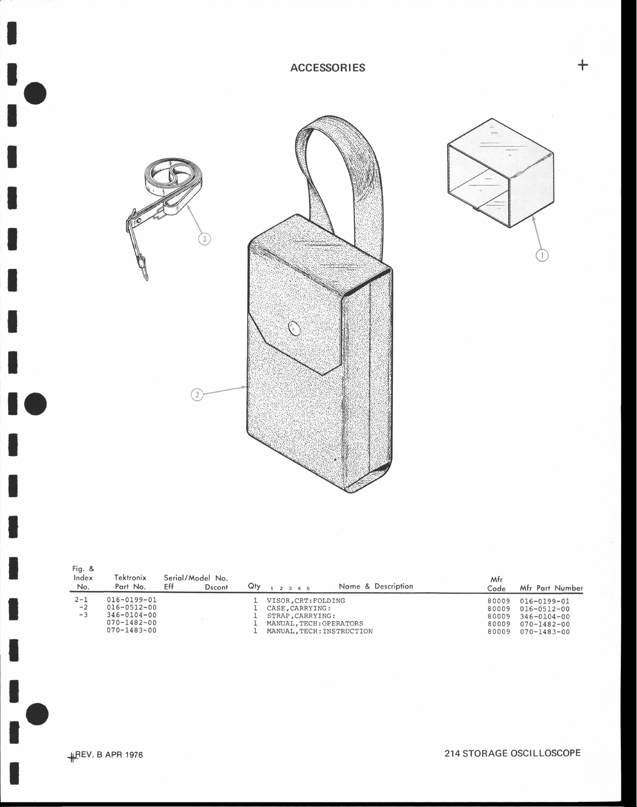
I
-
ro
I
t
I
I
I
I
I
ACCESSORIES
+
I
lo
I
I
I
I
r
I
I
I
Fis.
Index
No.
2-L
-2
-3
&
Tektronix
Pqrt
016-0199-01
015-0512-00
346-0104-00
07
0-1482-00
070-1483-00
No.
Seriol/Model
Eff
Dscont
No.
oty
1 VISOR,CRT:FOLDING
1
1 STRAP,CARRYING:
1 MANUAL,TECH:OPERATORS
I MANUAL,TECH:INSTRUCTTON
3 4
1z
CASE,CARRYING:
s
Nome &
Descriplion
Mfr
Code
80009 016-0199-01
80009
80009
80009 070-1482-00
80009 070-1483-00
Port
Mfr
016-0512-00
346-0104-00
Number
f.
I
..UFEV.
lr
B
APR 1976
4
21
STORAGE
LLOSCOPE
OSCI
Page 87

o:
I
I
I
I
I
I
ol
I
I
I
I
I
I
O:
Page 88

ro
I
t
I
I
I
I
I
to
I
I
At Tektronix,
by adding
are
Sometimes,
changes
change
A
are
duplication
manual
Because
instrument
List.
of
this instrument.
the
circuit
developed
immediately
information
single
change
carried in
may
is
correct as
of the
may
parts
The
customer.
MANUAL
we continually
and component improvements to
tested.
and
due to
into
on following
may
the manual
occur.
printed.
universal
different
be
used will in
They
Order replacement
CHANGE
strive to keep up with
printing
affect
lf no
are installed when necessary
and shipping requirements, we
printed
parts procurement problem,
no way
manuals. Hence,
pages.
several
until all
such
f rom those described in the Replaceable
sections. Since
changes are
change
SERVICE
alter or compromise the
parts
pages
from the
INFORMATION
latest
electronic developments
instruments as
our
your
manual may
the change information
permanently
appear
NOTE
Replaceable
following this
some electrical
performance
to ensure
prompt
Electrical
soon as they
get
can't
entered,
Electrical Parts
these
contain new
sheets
some
page,
your
parts
or
your
in
reliability
delivery
Parts
List.
to
t
I
I
t
I
to
Page 89

t
CALIBRATION
Calibration
This
chart
characteristics where
may not
calibration
DM
Test
Equipment
compares
be a total functional
procedure
501 replaces
PG
501 replaces 1
PG
502 replaces
PG
508 replaces 114
PG
506 replaces 106
067-0502-01
TM
significant
may be necessary.
7D13
108
107
108
111
115
210',
Chart
500
replacement.
TEST
product performance
specification differences
Comparlson
501
PG502-5Voutput
PG
502
Performance
better than equipment being replaced.
PG
506 - Positive-going
PG 506 - Does not
EQUIPMENT REPLACEMENT
to that
Additional
ns into
3.5
-SVoutputpulse;
ns Risetime
3.5
-
Risetime less than
1 ns; 10 ns
Pretrigger
delay
of replacement equipment is the same or
trigger
output signal at least 1 V;
High Amplitude
put,
60 V.
chopped feature.
of
50
pulse
have
support
Main
Gharacterlstlcs
O.
out-
of
occur,
instrumentation may
older Tektronix
are listed. In some cases the
3.0 ns into 50
108 - 10 V
1
108-l0Voutput
111 - Risetime 0.5 ns:
to
Pretrigger
delay
-
106
Positive and Negativegoing
signal, 50 ns and 1 V;
High
100 v.
0502-01
-
Comparator output
can be
chopped
ence voltage.
equipment.
needed or a change in
be
Q.
pulse
output
ns
Risetime
250 ns
pulse
trigger output
Amplitude output,
alternately
to a refer-
30
Only those
new
instrument
or
t
I
I
I
I
I
I
ll
NOTE:
REV
All TM
B, JUN
1904, 1908
067-0532-01
504 replaces
067-0532-01
TG
1978
067-06s0-00
501 replaces 180,
generator
500
SG 503 - Amplitude range
191
SG 503 - Frequency
SG 504
1804
181
184
outputs are short-proof.
TG
501 - Trigger
TG
501
TG
501
range
range
output-
marker
from
100 ns.
can be
at
output-
from
at a time.
output-
TM 500
p-p.
5 sec
a time.
sec
5
at
5 mV to 5.5 V
250 kHz to 250 MHz.
-
Frequency
slaved to
output
through
time-mark
generated
-
Trigger
slaved to market
output
through 100 ns.
time-mark can be
generated
-
Trigger
slaved to,marker
output from 5 sec
through 100 ns.
One time-mark can
generated
be
a time.
All
One
One
plug-ln
1908 - Amplitude range 40 mV
0532-01
0532-01 - Frequencyrange
1804 - Trigger
181 - Multiple time-marks
184
2901
Instruments require
10 V
to
-
Frequency range
65 MHz to 500 MHz.
100 Hz;
100 kHz. Multiple
time-marks
generated
eously.
-
Separate
pulses
sec;
ms; 10 and
-
Separate
pulses,
to 0.1
time-marks can be
generated
eously.
p-p.
500 MHz.65 MHz
pulses
1, 10, and
can
simultan-
trigger
1 and 0.1
of
10, 1, and 0.1
TM
gs.
1
trigger
from 5 sec
gs.
Multiple
simultan-
5O&serles
1,
be
10,
Power
I
t
I
I
I
t
o:
Module.
Page 90
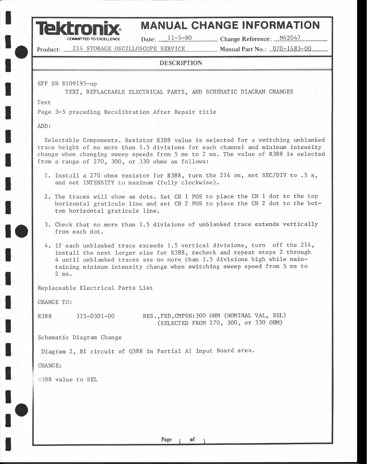
I
-o
I
I
I
TelGftrnix
6,ür,rrrEDrop(cEuFrrrcE
product:
EFI SN 8109195-up
Text
Page
ADD:
3-5
214
STORAGE
TEXT,
REPLACEABLE ELECTRICAL ?ARTS, AI{D SCIIEMAT IC
preceding
oSCIIIOSCOPE SERVICE.
Recallbratlon After Repair
MANUAL CHANGE
Date:
_11-5-80
DESCRIPTION
title
Change
Manual Part
INFORMATION
Reference'
DIAGRÄ!4 CIIANGES
No.:
y142047
070-1483-00
I
I
I
I
lo
I
I
I
I
SeLectable Components.
trace height of no
change when
frorn a range
1.
Install a 270 otnrs reslstor for R388, turn
and set IMENSITY
2. The traces !.ril-l- shorr
horlzontal
tom
3. Check that no more than
f rorn each dot.
4. If each unblanked trace exceeds
lnstall the next larger size
until unblanked traces are no
4
taini.ng mlnimum lntenslty change
2 ms.
Replaceable
CIIANGE TO:
R388
Schematic Diagram
changing sweep speeds from 5
of
horizontal
Electrical
315-0301-00
more than
27O,
graticule
Change
Resistor R388 value
1.5
300, or 330 ohms as follows:
maximum
to
as dots. Set CH
llne and set CH
gratlcule
Parts
Line.
1.5
List
RES.
is selected
dlvislons
(fully
divisions
1.5 vertlcal divisions,
for R388, recheck
more than
when svrltching
,FXD,CIVIPSN:300
(snr,ecrno
for each channel- and
ms
c1ocl,:wlse).
2 ms. The val-ue of
to
the
I POS to
2 POS to
of unblanked
1.5 diviolons
FR0M
214
place
place
and.repeat
sweep speed
(triOUrUAl
OIIM
270,
300,
for
a switching
minimun Lntenslty
R388 ls selected
set
on,
the CH
the CH
trace extends
SEc/DIv
I dot to the top
2 dot to the bot-
turn
high whlle
VAL, SEt)
330 olil{)
or
off the
steps 2 through
from 5
rmblanked
to
.5
vertlcally
214'
mainms to
s,
I
I
I
to
I
Diagram 2,
CIIANGE:
R388 value to SEL
Bl
circuit
of
Q388
in
Partial
A1 Input
of
Board
area.
Page 91

ol
I
I
I
I
I
I
I
ol
I
t
I
I
I
I
I
or
Page 92

Page 93

Page 94

lo
I
I
I
I
I
I
I
lo
I
I
I
I
I
I
I
ll
lo
Page 95

 Loading...