

Page 1

TECHNICAL MANUAL
OPERATOR, ORGANIZATIONAL, DIRECT SUPPORT,
AND GENERAL SUPPORT
MAINTENANCE MANUAL
(INCLUDING REPAIR PARTS)
FOR
OSCILLOSCOPE, TEKTRONIX, MODEL 212
NSN 6625-01-061-5519
MULTIPLE LAUNCH ROCKET SYSTEM
TM 9-6625-646-14&P
DEPARTMENT OF THE ARMY
JUNE 1984
Page 2

TM 9-6625-646-14&P
WARNING
DANGEROUS VOLTAGE
is used in the operation of this equipment
DEATH ON CONTACT
may result if personnel fail to observe safety precautions
Never work on electronic equipm ent unless ther e is another per son near by who is familiar
with the operation and hazards of the equipment and who is com petent in administering
first aid. When the technician is aided by operators, he must warn them about dangerous
areas.
Whenever poss ible, the power supply to the equipment must be s hut off befor e beginning
work on the equipment. Tak e particular care to ground every capacitor likely to hold a
dangerous potential. When working inside the equipment, after the power has been
turned off, always ground every part before touching it.
Be careful not to contact high-voltage connections when installing or operating this
equipment.
Whenever the nature of the operation permits, keep one hand away from the equipment
to reduce the hazard of current flowing through vital organs of the body.
WARNING
Do not be misled by the term "low voltage." Potentials as low as 50 volts may
cause death under adverse conditions.
COMMON and probe ground straps are electr ically connected. Theref ore, an elevated
reference applied to any is present on each - as indicated by the yellow warning bands
under the probe retractable hook tips.
For Artificial Respiration, refer to FM 21-11.
EXTREMELY DANGEROUS POTENTIALS
greater than 500 volts exist in the following units:
1. CRT Power Supply
2. Horizontal Deflection System
3. Vertical Deflection System
a/(b blank)
Page 3

TM 9-6625-646-14&P
Copyright 1972 by Tektronix, Inc. All rights reserved. REPRODUCED BY PERMISSION OF TEKTRONIX, INC. Distribution is limited
to use in connection with the Multiple Launch Rocket System.
Technical Manual HEADQUARTERS
DEPARTMENT OF THE ARMY
No. 9-6625-646-14&P Washington, D.C.,
8 June 1984
Operator’s, Organizational, Direct Support, and
General Support Maintenance Manual
(Including Repair Parts)
for
OSCILLOSCOPE, TEKTRONIX, MODEL 212
(NSN 6625-01-061-5519)
MULTIPLE LAUNCH ROCKET SYSTEM
REPORTING OF ERRORS
You can help improve this bulletin by calling attention to errors and by
recommending improvements and stating your reasons for the recommendations.
Your letter or DA Form 2028, Recommended Changes to Publications, s hould be
mailed directly to Commander, U.S. Army Missile Command, ATTN: DRSMISNPM, Redstone Arsenal, AL 35898. A reply will be furnished to you.
TABLE OF CONTENTS
Page
LIST OF ILLUSTRATIONS............................................................................................................................ iii
SECTION 0. GENERAL INFORMATION.......................................................................................... 0-1
Scope............................................................................................................................ 0-1
Indexes of publications................................................................................................. 0-1
SECTION 1. INTRODUCTION.......................................................................................................... 1-1
Option information........................................................................................................ 1-4
Accessories.................................................................................................................. 1-5
Manual change information.......................................................................................... 1-6
Calibration test equipment replacement....................................................................... 1-7
SECTION 2. FUNCTIONS OF CONTROLS AND CONNECTORS.................................................. 2-1
SECTION 3. PREVENTIVE MAINTENANCE.................................................................................... 3-1
Disassembly instructions.............................................................................................. 3-1
Cleaning........................................................................................................................ 3-1
Visual inspection........................................................................................................... 3-1
Semiconductor checks................................................................................................. 3-2
Recalibration................................................................................................................. 3-2
This manual is, in part, authenticated manufacturer’s commercial literature. A Maintenance Allocation Chart and Recommended Spare
Parts List has been added to supplement the commercial literature. The format of this manual has not been structured to consider
levels of maintenance.
i
Page 4

TM 9-6625-646-14&P
SECTION 4. CALIBRATION................................................................................................................ 4-1
Test equipment required................................................................................................. 4-1
Preliminary procedure..................................................................................................... 4-3
Preliminary control settings............................................................................................. 4-3
Procedure ....................................................................................................................... 4-4
SECTION 5. TROUBLESHOOTING AIDS.......................................................................................... 5-1
Component color-code ................................................................................................... 5-1
Semiconductor lead configurations ................................................................................ 5-2
Equipment recommended .............................................................................................. 5-2
SECTION 6. CIRCUIT DESCRIPTION................................................................................................ 6-1
Block............................................................................................................................... 6-1
Circuit operation.............................................................................................................. 6-1
SECTION 7. CORRECTIVE MAINTENANCE..................................................................................... 7-1
Obtaining replacement parts........................................................................................... 7-1
Component replacement ................................................................................................ 7-1
Instrument repackaging.................................................................................................. 7-4
SECTION 8. PARTS LIST, DIAGRAMS AND CIRCUIT BOARD ILLUSTRATIONS .......................... 8-1
Electrical parts list........................................................................................................... 8-2
Mechanical parts list....................................................................................................... 8-12
Exploded drawings.......................................................................................................... 8-17
Circuit board drawings and schematics.......................................................................... 8-19
APPENDIX A. REFERENCES ........................................................................................... A-1
B. MAINTENANCE ALLOCATION CHART (MAC)......................................... B-1
C. RECOMMENDED REPAIR PARTS LIST................................................... C-1
ii
Page 5

TM 9-6625-646-14&P
LIST OF ILLUSTRATIONS
Figure Title Page
1-1 212 Oscilloscope. 0-1
1-2 212 Oscilloscope Accessories. 1-5
2-1 Side Panel Controls and Connectors. 2-1
3-1 Location of Screws Securing Bottom Cover and Side Panel. 3-1
3-2 Location of Circuit Boards Within the 212. 3-2
4-1 Location of Power Supply Test Points and CRT Grid Bias
Adjustment. 4-4
4-2 Location of Trace Rotation Adjustment. 4-4
4-3 Location of Vertical Centering Adjustment and Test Point. 4-5
4-4 Location of Attenuator Compensation Capacitors. 4-7
4-5 Location of Horizontal Centering Adjustment and Test Point. 4-10
5-1 Color Code for Resistors, Ceramic Capacitors, and Dipped Tantalum
Electrolytic Capacitors. 5-1
5-2 Lead Configuration of Semiconductors Used in this Instrument. 5-2
6-1 Vertical Input Amplifiers Detailed Block Diagram. 6-2
6-2 Vertical and Horizontal Output Amplifiers Detailed Block Diagram. 6-3
6-3 Trigger/Sweep Generator Detailed Block Diagram. 6-4
6-4 Power Supply Detailed Block Diagram. 6-5
6-5 CRT Circuit Detailed Block Diagram. 6-6
7-1 Selecting C210 and C212 Capacitance Values for 48 to 52
Hz Operation. 7-2
7-2 Selecting C210 and C212 Capacitance Values for 58 to 62
Hz operation. 7-3
8-0 Mechanical Parts, Exploded View. 8-17
8-1 Block Diagram. 8-19
8-1A Al Input Circuit Board (Front). 8-21
8-1B Al Input Circuit Board (Near). 8-21
8-1C Waveform Conditions - Vertical Amplifier. 8-23
8-1D Vertical Amplifier Schematic Diagram. 8-23
8-1E Vertical Amplifier Schematic Diagram. 8-25
8-2 A2 Amplifier Circuit Board. 8-25
8-2A Waveform Conditions - Horizontal and Vertical Output Sweep
and Trigger. 8-27
8-2B Horizontal and Vertical Output Sweep and Trigger
Schematic Diagram. 8-27
8-3A A3 Power Supply Circuit Board, SN B040000-up. 8-29
8-3B A3 Power Supply Circuit Board, below SN B040000. 8-31
8-4 CRT Circuit Schematic Diagram. 8-33
8-5 Power Supply Schematic Diagram. 8-35
iii
Page 6

SECTION 0 GENERAL INFORMATION
TM 9-6625-646-14&P
O-1. Scope. This manual contains instructions for the
operator, organizational, direct support, and general
support maintenance of and calibration procedures for
Tektronix Oscilloscope, Model 212. Throughout this
manual, Tektronix Oscilloscope, Model 212 is referred
to as the 212.
O-2. Indexes of Publications.
Refer to the latest issue of DA Pam 310-4 to determine
whether there are new editions, changes, or additional
publications pertaining to Tektronix Oscillos cope, Model
212.
b. DA Pam 310- 7.
Pam 310-7 to determine whether there are modification
work orders (MWO’s) pertaining to Tektronix
Oscilloscope, Model 212.
O-3. Forms, Records, and Reports. Department of
Army forms and procedures used for equipment
maintenance and calibration are those prescr ibed by TM
38-750, The Army Maintenance Management System.
Accidents involving injury to personnel or damage to
materiel will be reported on DA Form 285, Accident
Report, in accordance with AR 385-40.
Refer to the latest issue of DA
a. DA Pam 310-4.
O-4. Reporting Equipment Improvement
Recommendations (EIR). If your 212 needs
improvement, let us know. Send us an EIR. You, the
user, are the only one who can tell us what you don’t like
about your equipment. Let us know why you don’t like
the design. Tell us why a procedure is hard to perform.
Put it on an SF 368 (Quality Deficiency Report). Mail it to
Commander, U.S. Army Missile Command, ATTN:
DRSMI-SNEM, Redstone Arsenal, AL 35898. We’ll send
you a reply.
O-5. Administrative Storage. To prepare the Tektronix
Oscilloscope, Model 212 for placement into and removal
from administrative storage, refer to Section 3, Chapter
4, AR 750-25-1, Maintenance of Equipment and
Supplies. Temporary storage should be acc omplished in
accordance with TB 750-25-1, Section 2, Maintenance
of Supplies and Equipment.
O-6. Destruction of Army Electronics Materiel.
Destruction of Tektronix Oscilloscope, Model 212 to
prevent enemy use shall be in accordance with TM 430002-26, Organizational Maintenance Manual,
Destruction of Equipment to Prevent Enemy Use for
Launcher, Rocket, Armored Vehicle Mounted: XM270,
Multiple Launch Rocket System.
0-1
Page 7
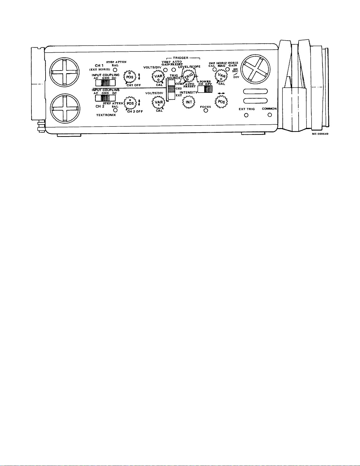
Figure 1-1. 212 Oscilloscope.
0-2
TM 9-6625-646-14&P
Page 8

SECTION 1
INTRODUCTION
TM 9-6625-646-14&P
The 212 Oscilloscope is a dual-channel portable
oscilloscope using all solid state and integrated circuitr y
(except the CRT). The s m all size of the 212 m ak es it an
extremely portable oscilloscope for on-location
maintenance in many fields of application.
The 500 kilohertz vertical system provides vertical
deflection factors from one millivolt (at a reduced
bandwidth) to 50 volts/division at the tip of either of the
two integral high-impedance probes. Both single-trace
and dualtrace modes of operation are offered. Singletrace displays are achieved by turning off either ver tical
channel with its position control. In the dual-trace mode,
the instrument automatically chops or alternates,
depending upon the sweep rate. The trigger circuits
provide stable triggering over the full bandwidth
capabilities of the vertical system.
The horizontal deflection system provides calibrated
sweep rates from 500 millisec onds to five m icrosec onds/
division. It also provides uncalibrated sweep rates, via a
variable sweep magnifier, to at least five times the
indicated sweep rate for a maximum of at least one
microsecond/ division. In addition, X-Y operation is
provided. Channel 1 supplies the horizontal (X)
deflection, with a range from less than one millivolt to 50
volts/division (at a reduced bandwidth of 50 kilohertz),
and Channel 2 the vertical (Y) deflection. The resultant
CRT display is presented on a 6 X 10 divis ion graticule
(each division equals 0.203 inch).
The 212 is operated either from AC line voltage or
from internal rechargeable batteries. The internal
batteries are recharged from the AC power line by the
integral battery charger.
This instrument will meet the following electrical
characteristics after complete instrument calibration.
These characteristics apply over an ambient temperature
of -15àC to +55àC (+5àF to +131àF), except as
otherwise indicated. W armup time for given accuracies
is five minutes.
VERTICAL DEFLECTION SYSTEM
Calibrated Range: One millivolt to 50 volt/division. 15
steps in 1-2-5 sequence.
Accuracy: Within 5% with VOLT S/DIV VAR control in
CAL position and gain correctly set at 5 mV/div.
Uncalibrated (variable) Range: Continuously variable
between calibrated settings. Extends maximum
deflection factor to at least 125 volts/division.
BANDWIDTH (with six-division reference):
10 mV/DIV to 50 V/DIV: DC to at least 500 kilohertz.
5 mV/DIV: DC to at least 400 kilohertz.
2 mV/DIV: DC to at least 200 kilohertz.
1 mV/DIV: DC to at least 100 kilohertz.
Lower Bandwidth Limit, AC (capacitively) Coupled:
about 2 hertz at all deflection factors.
INPUT RESISTANCE:
Approximately one megohm.
INPUT CAPACITANCE:
1 mV/DIV to 50 mV/DIV: Approximately 160
picofarads.
100 mV/DIV to 50 V/DIV: Approximately 140
picofarads.
MAXIMUM USABLE INPUT VOLTAGE:
50 V/DIV to .1 V/DIV: 600 volts (DC + peak AC). 600
volts peak-to-peak AC (five megahertz or less).
50 mV/DIV to 1 mV/DIV: 600 volts (DC + peak AC).
AC not over 2 kilohertz or risetime not less than 100
nanoseconds.
CHOPPED MODE:
From 500 ms/DIV to 2 ms/DIV of time base at
approximately 50 kilohertz.
ALTERNATE MODE:
From 1 ms/DIV to 5ps/DIV of time base.
INPUT IMPEDANCE MATCHING:
Matched to within approximately 10%.
DEFLECTION FACTOR:
1-1
Page 9

TM 9-6625-646-14&P
GAIN ACCURACY BETWEEN CHANNELS:
Within 5% with both VOLTS/DIV VAR controls in CAL
position and gain correctly set at 5 mV/DIV.
TRIGGERING
TRIGGER SENSITIVITY:
Internal: COMP: 0.2 division from DC to 500
kilohertz.
CH 2: 0.2 division from 2 hertz to 500 kilohertz.
External:
1.0 volt from DC to 500 kilohertz.
PRESET TRIGGER LEVEL:
Triggered at preset level on positive slope of
triggering signal. Sensitivity same as stated above.
DISPLAY JITTER:
0.5 microsecond or less at 500 kilohertz.
EXTERNAL TRIGGER:
Input Resistance: Approximately one megohm.
Input Capacitance: Approximately 30 picofarads.
Maximum Usable Input Voltage: 8 volts (DC + peak
AC) 16 volts peak-to-peak AC (one megahertz or less).
calibrated settings. Extends maxim um sweep rate to at
least 1.0 microsecond/division.
CH 1 HORIZONTAL INPUT:
Calibrated Deflection Factor: 1 millivolt to 50 volts/
division.
Variable: At least five times (using HORIZ MAG).
Accuracy: Within 10% (with HORIZ MAG control in
CAL position).
X-Y Phasing: Less than 3à at five kilohertz.
Maximum Input Voltage: 600 volts (DC + peak AC) ;
600 volts (peak-to-peak AC).
DISPLAY
GRATICULE:
Type: Internal black line, non-illuminated.
Area: Six divisions vertical by 10 divisions horizontal.
Each division equals 0.203 inch.
PHOSPHOR:
P31 Standard.
ISOLATION
HORIZONTAL DEFLECTION SYSTEM
SWEEP RATE:
Calibrated Range: 500 milliseconds to five
microseconds/ division. 16 steps in 1-2-5 sequence.
Accuracy (over center eight divisions): Within 5%
with HORIZ MAG control in CAL position and timing
correctly set at 1 ms/DIV (disregard f irs t 0.5 microsecond
of total sweep length).
Linearity (any two division portion within center eight
divisions): W ithin 5% (disregard f irst 10% of total sweep
length).
Variable Magnifier: Continuously variable between
PROBE COMMON TO 212 CASE EXTERIOR: (When
battery operated with AC power plug secured in the
insulated cover.) Maxim um s afe potential between pr obe
common (floating circuit ground) and 212 case exterior
not to exceed 500 V RMS sinusoidal, or 700 V (DC +
peak AC).
PROBE COMMON TO AC LINE: Maximum safe
potential between probe common (f loating c irc uit ground)
and the AC power line is not to exceed 250 V RMS
sinusoidal minus the AC power line RMS voltage. (i.e.,
when the AC power line RMS voltage is 117 V, the
maximum allowable potential on the probe common is
250 -117 = 133 V RMS.)
1-2
Page 10

AC OPERATION
CAUTION
Due to the capacitive line input
circuit, sudden voltage changes may
cause damaging input current
transients. Avoid operating this
instrument from squarewave inverter
supplies, or other sources that
produce large voltage transients.
LINE VOLTAGE RANGE: 110 to 126 volts, AC.
Batteries can not be charged during AC operation.
Instrument can be operated between 104 and 110 volts
with resulting slow discharge of internal batteries.
TM 9-6625-646-14&P
CHARGE OPERATING TEMPERATURE
TEMPERATURE 15°C +20°C to +30°C +55°C
(+5°F) (+68°F to +860F) (+131°F)
0°C (+32°F) 40% 60% 50%
+20àC to +30àC 65% 100% 85%
(+68° F to +86à F)
40°C (+104àF) 40% 65% 55%
GENERAL
ENVIRONMENT:
Temperature:
LINE FREQUENCY: 58 to 62 hertz.
NOTE
Refer to Option and Corrective
Maintenance information for other
line voltages and frequencies.
MAXIMUM POWER CONSUMPTION: Three watts or
less at 126 volts, 60 hertz.
INTERNAL BATTERY OPERATION
BATTERIES: 10 rechargeable A nickel-cadmium cells.
CHARGE TIME (from AC line): 16 hours f or full charge
(instrument off during charge cycle).
POWER (BAT TERY) INDICATOR: When ex tinguished,
indicates less than 10 minutes of sc ope operating life left
in the batteries.
BATTERY EXCESSIVE DISCHARGE PROTECTION:
Instrument operation automatically interrupted when
battery charge drops to 10 volts +0.5 volt.
TYPICAL OPERATING TIME (at maximum trace
intensity after full charge cycle at +20àC to +30àC):
Three to five hours. Longest operating tim e provided at
lower trace intensity.
Operating from Batteries , -15°C to +55 àC (+5àF to
+131àF).
Charging or operating from AC line, 0°C to +40°C
(+32°F to +104àF).
Storage, -40àC to +60°C (-40àF to +140à F).
Altitude:
Operating, to 25, 000 feet (maximum operating
temperature decreased by 10C per 1, 000 f eet above 15,
000 feet).
Non-operating, to 50, 000 feet.
Humidity (operating and non-operating): 5 cycles
(120 hours) to 95% relative humidity referenced to
MIL-E-16400F.
Shock (operating and non-operating): Tested with
two shocks at 150 g, one-half sine, two millisecond
duration each direction along three major axes.
WEIGHT (without accessories):
3.4 pounds (1.5 kilograms)
DIMENSIONS (measured at maximum points):
TYPICAL CHARGE CAPACITY (reference to charge/
discharge at +20àC to +30àC):
Height: 3.0 inches (7.6 centimeters).
Width: 5.25 inches (13.2 centimeters).
Depth: 8.9 inches (22.6 centimeters).
1-3
Page 11

TM 9-6625-646-14&P
OPTION INFORMATION
Your instrument may be equipped with one or more options. T his s ection desc ribes thos e options or dir ects the reader
to where the option is documented.
OPTION 1
Option 1 equips the 212 for operation from a 220 to 250 V ac 48 to 52 Hz power line source. O ption 1 parts values that
differ from the standard 212 are listed here. A power cord cable assembly, for adapting to appropriate power plugs, is
included with Option 1 instruments. Refer to the Corrective Maintenance and Diagrams sections of this manual for
additional information concerning Option 1.
ELECTRICAL PARTS LIST DIFFERENCES FOR OPTION 1
A3 670-2405-21* POWER SUPPLY Circuit Board Assembly (Option 1)
C204 283-0279-00 0.001 UF, 20%, 3 KV
C210 285-0932-00 1.0 UF, 10%, 400V
C212 285-0933-00 2.0 UF, 10%, 400V
C215 283-0279-00 0.001 UF, 20%, 3 KV
ADDITIONAL STANDARD ACCESSORIES FOR OPTION 1
161-0077-01 CABLE ASSEMBLY, POWER
(Adapts to users plug type)
*In some Option 1 instruments, the suffix number on the board may not be marked -21.
OPTION 2
Option 2 equips the 212 for operation from a 90 to 110 V ac 48 to 52 Hz power line source. Option 2 parts values that
differ from the standard 212 are listed here. Refer to the Corr ective Maintenance and Diagrams s ections of this manual
for additional information concerning Option 2.
ELECTRICAL PARTS LIST DIFFERENCES FOR OPTION 2
A3 670-2405-31 ** POWER SUPPLY Circuit Board Assembly (Option 2)
C210 285-0934-00 2.2 UF, 10%, 200V
C212 285-0935-00 4.4 UF, 10%, 200V
**ln some Option 2 instruments, the suffix number on the board may not be marked -31.
1-4
Page 12
TM 9-6625-646-14&P
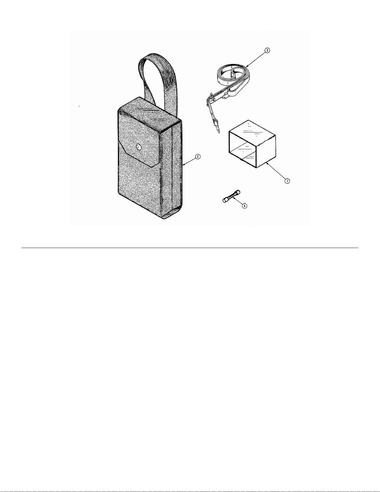
Fig. &
Index Tektronik Serial/Model No. Mfr
No. Part No. Eff Dscont Qty 1 2 3 4 5 Name & Description Code Mfr Part Number
-1 015-0199-01 1 VISOR, CRT: 80009 016-0199-01
-2 016-0512-00 1 CASE, CARRYING: 80009 016-0512-00
-3 346-0104-00 1 STRAP, CARRYING: 17516 4188-BA
-4 159-0121-00 2 FUSE, CARTRIDGE :DIN, 0.4A, 250V,5 SEC 75915 212.400
070-1375-00 1 MANUAL, TECH: OPERATORS 80009 070-1375-00
070-1376-00 1 MANUAL, TECH: INSTRUCTION 80009 070-1376-00
Figure 1-2. 212 Oscilloscope Accessories
1-5
Page 13

TM 9-6625-646-14&P
MANUAL CHANGE INFORMATION
At Tektronix, we continually strive to keep up with latest electronic developments by adding circuit and component
improvements to our instruments as soon as they are developed and tested.
Sometimes, due to printing and s hipping requirements, we can’t get these changes imm ediately into printed manuals.
Hence, your manual may contain new change information on following pages.
A single change may affect sever al sections. Since the change inform ation sheets are c arried in the manual until all
changes are permanently entered, some duplic ation may occur. If no such change pages appear following this page, your
manual is correct as printed.
SERVICE NOTE
Because of the universal parts procurement problem, some electrical parts in your instrument may be different
from those described in the Replaceable Electrical Parts List. The parts used will in no way alter or compromise
the performance or reliability of this instrument. They are installed when necessary to ensure prompt delivery to
the customer. Order replacement parts from the Replaceable Electrical Parts List.
1-6
Page 14

TM 9-6625-646-14&P
CALIBRATION TEST EQUIPMENT REPLACEMENT
Calibration Test Equipment Chart
This chart compares TM 500 produc t perform ance to that of older Tek tronix equipm ent. Only those characteris tics where
significant specification differences occur, are listed. In some cases the new instrument may not be a total functional
replacement. Additional support instrumentation may be needed or a change in calibration procedure may be necessary.
Comparison of Main Characteristics
DM 501 replaces 7D13
PG 501 replaces 107 PG 501 - Risetime less than 3.5 ns into 107 - Risetime less than 3.0 ns into
108 PG 501 - 5 V output pulse; 3.5 ns Risetime. 108 - 10 V output pulse; 1 ns Risetime.
111 PG 501 - Risetime less than 3.5 ns; 8 ns 111 - Risetime 0.5 ns; 30 to 250 ns
114 PG 501 + 5 V output. 114 - ±10 V output. Short proof output.
115 PG 501 - Does not have Paired, Burst, Gated, 115 - Paired, Burst, Gated, and Delayed
PG 502 replaces 107
108 PG 502 - 5 V output 108 - 10 V output.
111 PG 502 - Risetime less than 1 ns; 10 ns 111 - Risetime 0.5 ns; 30 to 250 ns
114 PG 502 -+5 V output 114 - 10 V output. Short proof output.
115 PG 502 - Does not have Paired, Burst, Gated, 115 - Paired, Burst, Gated, Delayed & Un-
2101 PG 502 - Does not have Paired or Delayed 2101 - Paired and Delayed pulse; 10 V
PG 506 replaces 106 PG 506 - Positive-going trigger output signal 106 - Positive and Negative-going trigger
067-0502-01 PG 506 - Does not have chopped feature. 0502-01 - Comparator output can be alter-
SG 503 replaces 190,
190A, 190B SG 503 - Amplitude range 5 mV to 5.5 V p-p. 190B - Amplitude range 40 mV to 10 V p-p.
191 SG 503 - Frequency range 250 kHz to 250 MHz. 191 - Frequency range 350 kHz to 100 MHz.
067-0532-01 SG 503 - Frequency range 250 kHz to 250 MHz. 0532-01 - Frequency range 65 MHz to 500
TG 501 replaces 180,
180A TG 501 - Marker outputs, 5 sec to 1 ns. 180A - Marker outputs, 5 sec to 1 us.
181 TG 501 - Marker outputs, 5 sec to 1 ns. Sine- 181 - Marker outputs, 1, 10, 100, 1000,
184 TG 501 - Marker outputs, 5 sec to 1 ns. Sine- 184 - Marker outputs, 5 sec to 2 ns. Sine-
2901 TG 501 - Marker outputs, 5 sec to 1 ns. Sine- 2901 - Marker outputs, 5 sec to 0.1 us.
50Ω.50Ω.
Pretrigger pulse delay. Pretrigger Pulse delay.
or Delayed pulse mode; +5 V dc pulse mode; +
Offset. Has +5 V output. Short-proof output.
Pretrigger pulse delay. Pretrigger pulse delay.
Delayed & Undelayed pulse mode; delayed pulse mode; +10 V output.
Has ±5 V output. Short-proof output.
pulse. Has ±5 V output. output.
at least 1 V; High Amplitude out- output signal, 50 ns and 1 V; High
put, 60 V. Amplitude output, 100 V.
nately chopped to a reference
voltage.
MHz.
Sinewave available at 5, 2, and 1 ns. Sinewave available at 20, 10,
Trigger output - slaved to marker and 2 ns. Trigger pulses 1, 10,
output from 5 sec through 100 ns. 100 Hz; 1, 10, and 100 kHz.
One time-mark can be generated at a Multiple time-marks can be
time. generated simultaneously.
wave available at 5, 2, and 1 ns. and 10, 000 us, plus 10 ns sinewave.
wave available at 5, 2, and 1 ns. wave available at 50, 20, 10, 5,
Trigger output - slaved to marker and 2 ns. Separate trigger pulses
output from 5 sec through 100 ns. of 1 and .1 sec; 10, 1, and .1 ms;
One time-mark can be generated at 10 and 1 /s. Marker amplifier proa time. vides positive or negative time
marks of 25 V min. Marker
intervals of 1 and .1 sec; 10, 1,
and .1 ms; 10 and 1 us.
wave available at 5, 2, and 1 ns. Sinewave available to 50, 10,
Trigger output - slaved to marker and 5 ns. Separate trigger
output from 5 sec through 100 ns pulses, from 5 sec to 0.1 us.
One time-mark can be generated at Multiple time-marks can be genea time. rated simultaneously.
10 V output.
NOTE: All TM 500 generator outputs are short-proof. All TM 500 plug-in instruments require TM 500-Series
Power Module.
1-7
Page 15
TM 9-6625-646-14&P
1-8
Page 16
SECTION 2
FUNCTIONS OF CONTROLS AND CONNECTORS
TM 9-6625-646-14&P
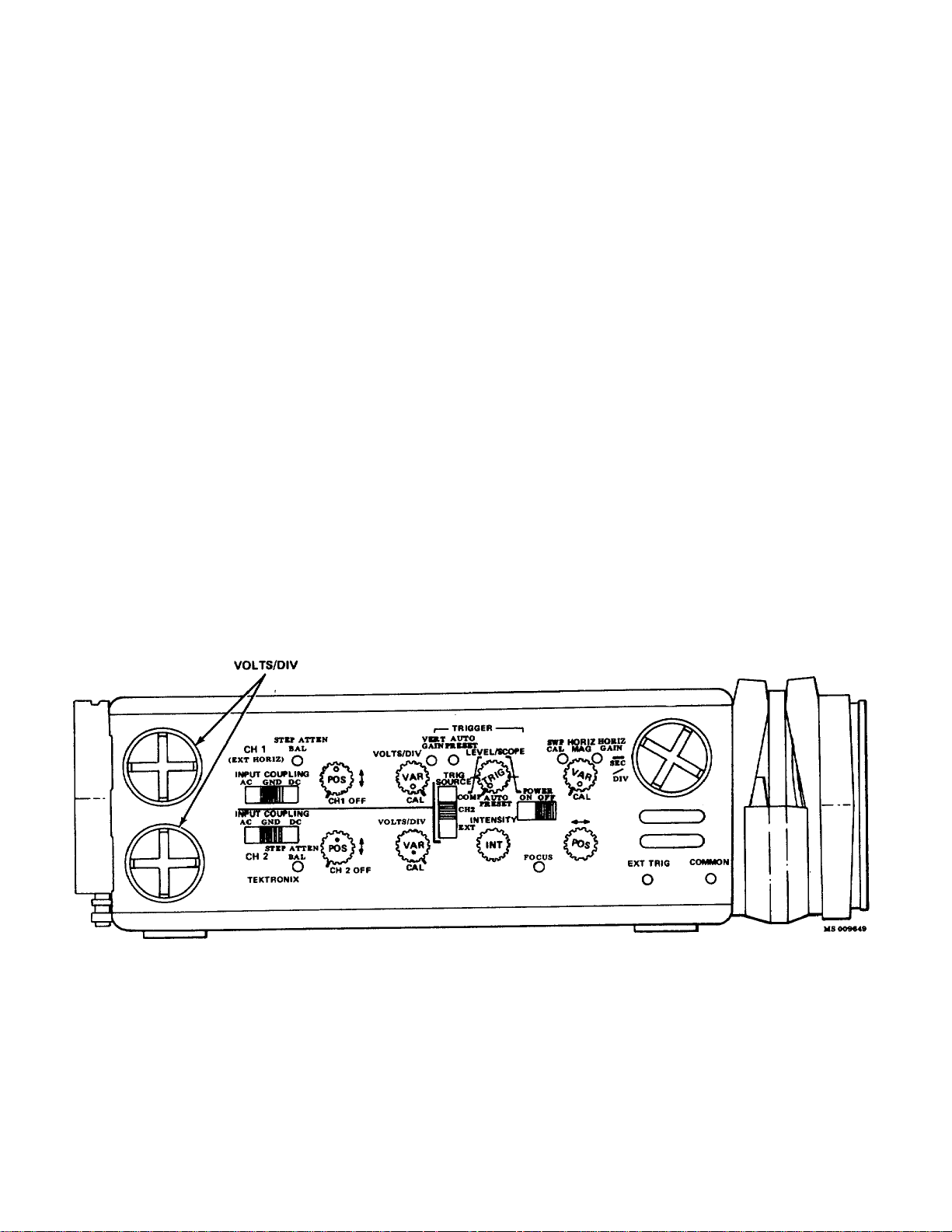
The controls and connectors neces sary for operation
of the 212 are located on the right side of the instrument.
(See Fig. 2-1.) The POWER (BATTERY) indicator is on
the front panel. A brief description of each contr ol and
connector is given here.
VOLTS/DIV-selects vertical deflection factor (vertical
VARiable control must be in CAL position for
indicated deflection.
INPUT COUPLING-selects the method used to couple
the channel input signal to the vertical amplifier
system.
AC-the DC component of input signal is blocked.
GND-vertical amplifier input circuit is grounded.
The applied input signal is connected to ground
through a one megohm resistor to provide a
precharge path for the AC input coupling
capacitor.
DC-all components of the input signal are
passed to the vertical amplifier system input.
STEP ATTEN BALance-a screwdriver adjustment to
balance the vertical amplifier system for minimum
trace shift when switching deflection factors.
Vertical POSition-controls the vertical position of the
appropriate trace. OFF detent turns the channel
off.
VOLTS/DIV VARiable-provides a continuously variable
deflection factor between the calibrated settings of
the VOLTS/DIV switch for the appropriate vertical
channel.
VERTical GAIN-screwdriver adjustment to set the gain of
the vertical amplifier system.
AUTO PRESET-screwdriver adjustment to set the AUTO
PRESET trigger point for automatic trigger
operation.
Trigger SOURCE-selects the source of the trigger signal.
COMP-the sweep is triggered from a sample of
the vertical deflection signal after the vertical
switching.
CH 2-the sweep is triggered from a sample of
the vertical deflection signal before the vertical
switching and only from CH 2.
EXT-the sweep is triggered from the signal
applied to the EXT TRIG banana jack.
Figure 2-1. Side Panel controls and connectors.
2-1
Page 17

LEVEL/SLOPE-selects the amplitude point and the s lope
of the trigger signal on which the sweep is triggered.
When the indicator dot is to the left of center, the
sweep is triggered on the positive-going slope of the
trigger signal; to the right of center, on the negative-
going slope. When the LEVEL/SLOPE control is set
to the AUTO PRESET detent, the sweep is
automatically triggered at a preset level on the
positive-going slope.
INTENSITY-controls brightness of CRT display.
TM 9-6625-646-14&P
Horizontal POSition-controls the horizontal position of the
trace.
SEC/DIV-selects horizontal sweep rate (HORIZ MAG
must be in CAL position for indic ated sweep rate) X-Y
position allows for X-Y operation; CH 2 supplies the
vertical deflection and CH 1 the horizontal deflection.
EXT TRIG-banana jack for input of an external trigger
signal.
SWP CAL-screwdriver adjustment to provide calibrated
sweep timing.
POWER-controls power to the instrument. Does not
interrupt charging current to the internal batteries
when the instrument is connected to an AC line
voltage.
FOCUS-screwdriver adjustm ent to obtain a well-defined
display.
HORIZontal MAGnifier-provides continuously variable
sweep magnification to a max imum of approxim ately
five times the sweep rate indicated by the SEC/DIV
switch.
HORIZontal GAIN-screwdriver adjustment to set the
basic gain of the horizontal amplifier system.
COMMON-banana jack to establish common ground
between the 212 and the external signal source or
equipment under test.
WARNING
COMMON and probe ground straps
are electrically connected. Therefore,
an elevated reference applied to any
is present on each - as indicated by
the yellow warning bands under the
probe retractable hook tips.
POWER ( BATTERY) Indicator-red light to indicate when
the instrument is on. When light extinguishes, less
than 10 minutes of operating life remain.
2-2
Page 18
SECTION 3
PREVENTIVE MAINTENANCE
Preventive maintenance, when performed on a
regular basis, can prevent instrument breakdown and
may improve the reliability of this instrument. The
severity of environment to which the 212 is subj ected will
determine the frequency of maintenance. A convenient
time to perform preventive maintenance is preceding
recalibration of the instrument.
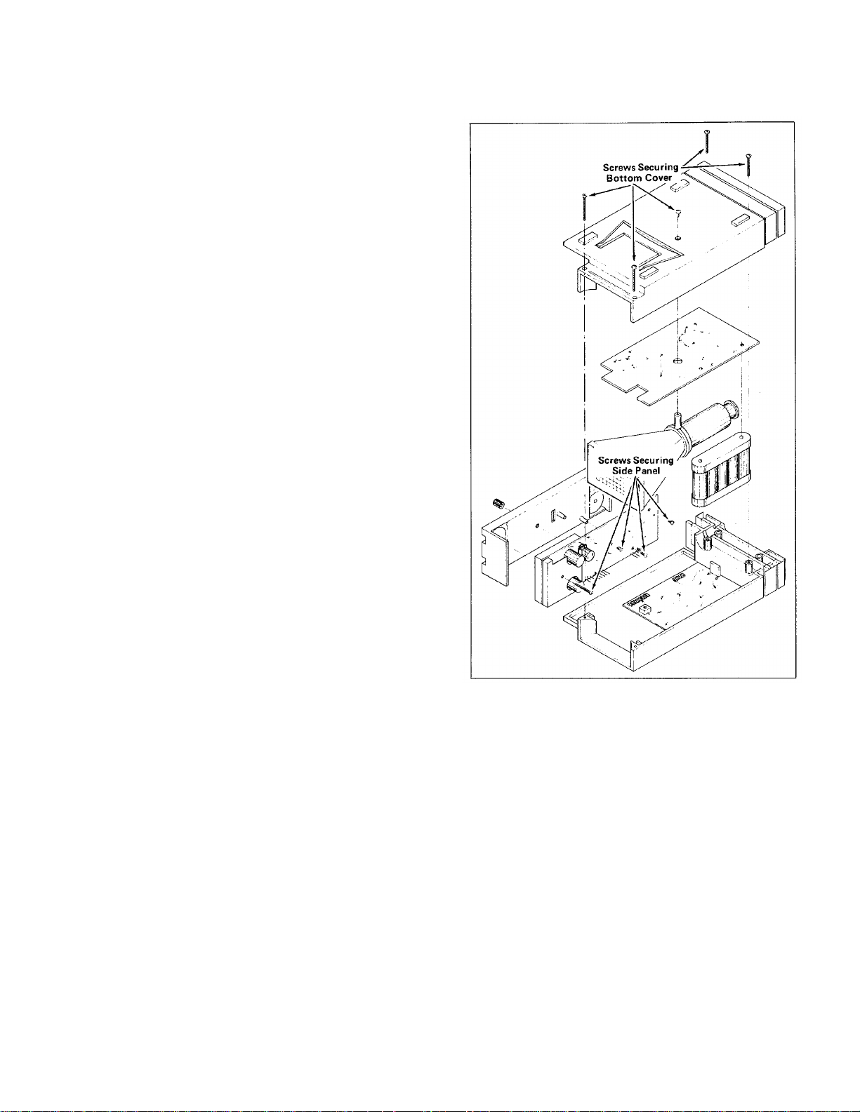
Disassembly
To gain access to the interior of the instrument,
unwind both the probe cords and the power cord from
the rear of the instrument. Remove the five screws in
the bottom cover of the instrument. See Fig. 3- 1. G ently
separate the bottom cover from the instrument and lay
aside. The Power Supply circuit board with the batteries
can be lifted up and pivoted out of the way. Most of the
internal workings of the instrument are now accessible.
If it is necessary to have access to the front of the
Input circuit board, remove the knobs from all of the
external control shafts. Remove the four screws
securing the side panel to the Input circuit board and
remove the instrument side panel.
TM 9-6625-646-14&P
Cleaning
The 212 should be cleaned as often as operating
conditions require. Accumulation of dir t in the inst rument
can cause component breakdown.
The high impact plastic covers provide protection
against dust in the interior of the instrument. Loos e dust
accumulated on these covers can be removed with a soft
cloth or small brush. The brush is also useful for
dislodging dirt on and around the side-panel controls.
Dirt which remains can be removed with a soft cloth
dampened in a mild detergent and water solution.
Abrasive cleaners should not be used.
It should be only occasionally necessary to c lean the
interior. The best way to clean the interior is to blow off
the accumulated dust with dry, low-velocity air. A
softbristle brush or a cotton-tipped applicator is useful for
cleaning in narrow spaces or for cleaning more delic ate
circuit components.
Figure 3-1. Location of screws securing bottom cover and
side panel.
CAUTION
Avoid the use of chemical cleaning
agents which might damage the
plastics used in this instrument.
Avoid chemicals which contain
hydrochloric acid, sodium hydroxide,
or sulfuric acid.
Visual Inspection
The 212 should be inspected occasionally for such
defects as broken connections, improperly seated
transistors, damaged circuit boards, and heat-damaged
parts.
3-1
Page 19
parts. The corrective procedure for most visible defects
is apparent; however, particular care must be taken if
heat-damaged components are found. Overheating
usually indicates other trouble in the instrument;
therefore, it is important that the cause of the
overheating be corrected to prevent recurrence of the
damage.
Semiconductor Checks
Periodically checking the semiconductors in the 212 is
not recommended. The best check of semiconductor
performance is actual operation in the instrument. If it is
desired to check the performance of a semiconductor
out of the instrument, a dynamic checker such as a
TEKTRONIX Type 576 Transistor Curve Tracer is
recommended. Lead configurations of the
semiconductors used in the 212 are shown in Fig. 5-2.
An extracting tool should be used to remove the 14-,
and 16-pin flat integrated circuits to prevent damage to
the pins. If an extracting tool is not available when
removing one of these integrated circuits, pull s lowly and
evenly on both ends of the device. Try to avoid having
one end of the integrated circuit disengage from the
socket before the other, as the pins may be damaged.
When replacing semiconductors, key the
semiconductor’s index with that of its soc ket. Failure to
do so can result in damaged components.
TM 9-6625-646-14&P
Recalibration
To assure accurate measurements, check the
calibration of this instrument after each 1000 hours of
operation or every six months if used infrequently. In
addition, replacement of components may necessitate
recalibration of the affected circuits. The calibration
procedure can also be helpful in localizing certain
troubles in the instrument. In some cases, minor
troubles may be revealed or corrected by recalibration.
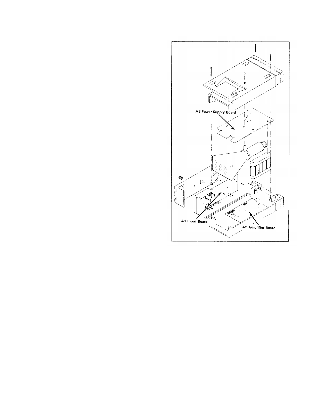
Figure 3-2. Location of circuit boards within the 212.
3-2
Page 20

SECTION 4
CALIBRATION
TM 9-6625-646-14&P
General
To assure instrument accuracy, check the calibration
of the 212 every 1000 hours of operation, or every six
months if used infrequently. Before complete calibr ation,
throughly clean and inspect this instrument as outlined in
the Preventive Maintenance section.
The following test equipment and accessories, or their
equivalent, are required for complete calibration of the
212. Given specifications for the test equipment are the
minimum necessary for acc urate calibration. Therefore,
the specifications of any test equipment must either meet
TEST EQUIPMENT REQUIRED
or exceed those listed below. All test equipment is
Tektronix, Inc., provides complete instrument repair
and recalibration at local Field Service Centers and the
Factory Service Center. Contact your local TEKTRONIX
Field Office or representative for further information.
assumed to be correctly calibrated and operating within
the listed specifications. Detailed operating instruc tions
for the test units are not given in this procedure. Refer to
the instruction manual for the test equipment if more
information is needed.
To aid in locating a step in this procedure, an index is
given prior to the complete procedure. Completion of
each step in the Calibration procedure ensur es that this
Special Calibration Fixtures
instrument meets the electrical specifications given in the
Introduction of this manual. Where possible, instrument
performance is checked before an adjustment is made.
For best overall instrument performance, make each
adjustment to the exact setting even if the CHECK- s tep
is within the allowable tolerances.
Special TEKTRONIX Calibration fixtures are used in
this procedure only where they facilitate instrument
calibration. These special calibration fixtures are
available from Tektronix, Inc. Order by part number
through your local TEKTRONIX Field Office or
representative.
TABLE 4-1.
TEST EQUIPMENT
Description Minimum Specifications Usage Example
1. Time-Mark Generator Marker outputs, 5 microseconds to 0.1 Horizontal timing check a. TEKTRONIX 2901
second; marker accuracy, within 0.1%. and adjustment. Time-Mark Generator.
b. TEKTRONIX 184
Time-Mark Generator.
2. Standard Amplitude Amplitude accuracy, 0.25%; signal Vertical and horizontal a. TEKTRONIX
Calibrator amplitude, 5 millivolts to 100 volts; amplifier gain checks and calibration fixture Part
output signal one-kilohertz square adjustments. Number 067-0502-01.
wave.
3. Square-Wave Frequency, one kilohertz; risetime, Vertical amplifier a. TEKTRONIX Type
Generator 100 nanoseconds or less; output compensation checks and 106 Square-Wave
amplitude, 0.4 volt to 40 volts. adjustments. Generator.
4. Low-Frequency Frequency, one kilohertz to 500 Vertical Amplifier a. General Radio
Constant-Amplitude kilohertz; output amplitude, at least bandwidth check. Trigger 1310-B Oscillator.
Signal Generator 200 millivolts. operation checks.
5. DC Voltmeter Range, zero to 1000 volts; accuracy, Power supply output level a. Triplett Model
within 3%; input impedance, checks. Vertical and 630-NA.
20, 000Ω/volt. horizontal centering
adjustment. CRT grid bias b. Simpson Model 262.
adjustment.
4-1
Page 21

TM 9-6625-646-14&P
TABLE 4-1 (cont)
Description Minimum Specifications Usage Example
6. Cable Impedance, 50 ohms; type, RG-58/U; External trigger operation a. TEKTRONIX Part
length, 42 inches; connectors, BNC. check. Horizontal gain Number 012-0057-01.
check and adjustment.
7. Adapter Connectors, BNC female and dual External trigger checks. a. TEKTRONIX Part
banana plug. Number 103-0090-00.
8. Adapter Connectors, GR874 and BNC female. Vertical Amplifier a. TEKTRONIX Part
compensation checks and Number 017-0063-00.
adjustment.
9. Termination Impedance, 50 ohms; accuracy, 2%; Vertical amplifier a. TEKTRONIX Part
connectors, BNC. compensation checks and Number 011-0049-01.
adjustment.
10. Attenuator Ratio, 10X; connectors, BNC; Vertical amplifier a. TEKTRONIX Part
impedance, 50 ohms. bandwidth check. Number 011-0059-01.
11. Adapter Connectors, probe tip to BNC. Used throughout a. TEKTRONIX Part
procedure for signal Number 013-0084-01.
interconnection.
12. T-Connector Connectors, BNC. External trigger operation a. TEKTRONIX Part
checks. Number 103-0030-00.
13. Screwdriver Three-inch shaft, 3/32 inch bit. Used throughout a. Xcelite R-3323.
Procedure to adjust
variable resistors.
14. Low-Capacitance 1 1/2-inch shaft. Used to adjust variable a. TEKTRONIX Part
Screwdriver capacitors. Number 003-0000-00.
INDEX TO CALIBRATION PROCEDURE
Power Supply and Display
1. Check Power Supply DC Levels
2. Adjust CRT Grid Bias (internal adjustment of
R273)
3. Adjust FOCUS (external side panel adjustment
of R398)
4. Adjust Trace Rotation (internal adjustment of
R141)
Vertical System Adjustment
5. Adjust Vertical DC Centering (internal
adjustment of R101)
6. Adjust CH 1 STEP ATTENuation BALance
(external
side panel adjustment of R415)
7. Adjust CH 2 STEP ATTENuation BALance
(external side panel adjustment of R315)
8. Adjust VERTical GAIN (external side panel
adjustment of R470)
9. Check CH 2 VARiable VOLTS/DIV Range
10. Check CH 2 VOLTS/DIV Accuracy VOLTS/DIV
Range
11. Check CH 1 VOLTS/DIV Accuracy and VARiable
12. Adjust CH 1 VOLTS/DIV Switch Compensation
(internal side panel adjustment of C407, C408, C409)
13. Adjust CH 2 VOLTS/DIV Switch Compensation
(internal side panel adjustment of C307, C308, C309
14. Check CH 2 Vertical Amplifier Bandwidth
4-2
Page 22

TM 9-6625-646-14&P
15. Check CH 1 Vertical Amplifier Bandwidth
Trigger Circuit Adjustment
16. Adjust AUTO PRESET (external side panel
adjustment of R375)
17. Check Trigger Circuit Operation
Horizontal System Adjustment
18. Adjust Hor izontal Centering (internal adjustm ent
of R366)
19. Adjust HORIZontal GAIN (external side panel
adjustment of R475)
20. Adjust SWEEP CALibration (external side panel
adjustment of R370)
21. Check HORIZ MAG Range
22. Check SEC/DIV Accuracy
PRELIMINARY PROCEDURE
NOTE
Titles for external controls of this
instrument are fully capitalized in this
procedure (e.g., INTEASITY). Internal
adjustments are initial capitalized
only (e.g., Grid Bias).
PRELIMINARY CONTROL SETTINGS
Preset the instrument controls to the settings given
below when starting a calibration procedure.
Channel 1 Controls
VOLTS/DIV 5 m
VOLTS/DIV VAR CAL
POS Midrange
INPUT COUPLING GND
Channel 2 Controls
VOLTS/DIV 5 m
VOLTS/DIV VAR CAL
POS OFF
INPUT COUPLING GND
This instrument should be adjusted at an ambient
temperature of +250C (+ 50C) for best overall accuracy.
1. Remove the instrument covers as described in
the Disassembly Instructions in the Preventive
Maintenance section.
2. Connect the instr ument to a 117 VAC 60 Hz line
source. If the batteries are not fully charged, leave the
212 connected to the line with the power switch turned
off for a period of approximately one hour before
continuing with calibration.
3. Set the instrument controls as given under
Preliminary Control Settings. Allow at least five minutes
of warmup before proceeding.
Trigger Controls
SOURCE COMP
LEVEL/SOURCE AUTO PRESET
Sweep Controls
SEC/DIV 1 m
HORIZ MAG CAL
POS Midrange
Display Controls
POWER ON
INTENSITY Fully Counterclockwise
4-3
Page 23
CALIBRATION PROCEDURE
POWER SUPPLY and DISPLAY
Equipment Required
1. DC Voltmeter 2. Three-inch Screwdriver
TM 9-6625-646-14&P
Control Setting
Preset instrument controls to the settings given under
Preliminary Control Settings.
1. Check Power Supply DC Levels
NOTE
If the instrument has been operating
satisfactorily prior to recalibration,
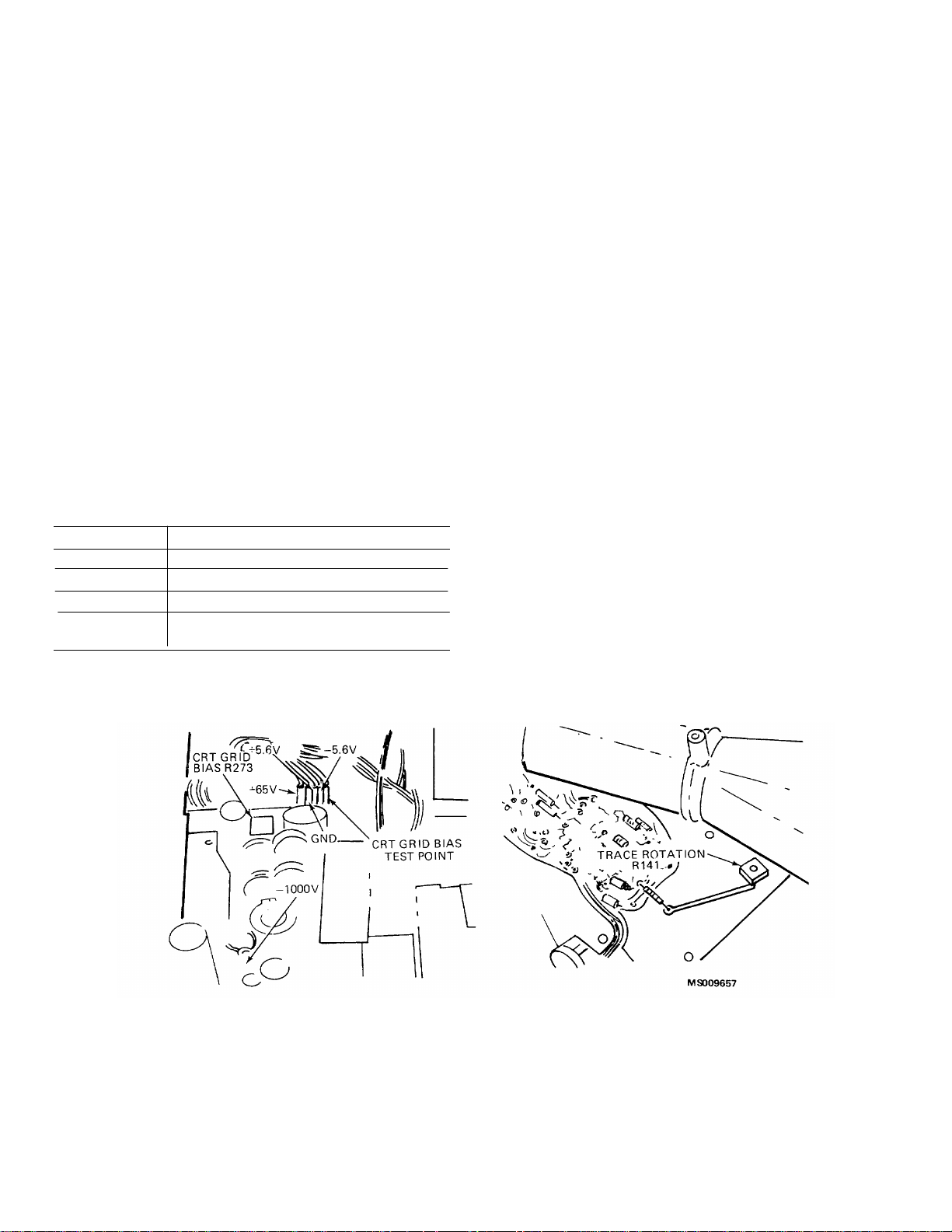
proceed with step 2.
a.Using the DC voltmeter, measure the DC level of
the power supplies given in Table 4-2. Observe proper
meter polarity. See Fig. 4-1 for test point locations.
TABLE 4-2.
Power Supply Accuracy
Supply Measurement
-5.6 volt -5.6 volts ±0.4 volt
+5.6 volt +5.6 volts ±0.4 volt
+65 volt +65 volts ±4 volts
-1000 volt -960 volts ±40 volts
(due to meter loading)
2 of plug P3 (negative meter lead to pin 2) on the Power
Supply Board. See Fig. 4-1.
b.Turn the INTENSITY control fully clockwise.
c.CHECK-Meter reading of +1.9 volts.
d.ADJUST-CRT Grid Bias, R273 (s ee Fig. 4-1) for
a meter reading of +1.9 volts.
e.Disconnect all test equipment. Turn the
INTENSITY control fully counterclockwise.
3. Adjust FOCUS
a.Turn CH 2 POS midrange and CH 1 POS to the
OFF detent.
b.Set the SEC/DIV switch to X-Y and adjust the
INTENSITY control for a nominal display intensity.
c.ADJUST-FOCUS, R398 (located on the 212 side
panel) for a well-defined dot.
4. Adjust Trace Rotation
a.Set the SEC/DIV switch to 1 m.
b.CHECK-Free-running sweep is parallel with a
horizontal graticule line.
c.ADJUST-Trace Rotation, R141 (see Fig. 4-2) s o
the trace is parallel with the center horizontal graticule
line.
2. Adjust CRT Grid Bias
a.Connect the DC voltmeter between pin 5 and pin
Figure 4-1. Location of power supply test points and CRT
Grid Bias
adjustment.
Figure 4-2. Location of Trace Rotation adjustment.
4-4
Page 24
VERTICAL SYSTEM ADJUSTMENT
Equipment Requested
TM 9-6625-646-14&P
1.Standard Amplitude Calibrator
2.Square-Wave Generator
3.Low Frequency Constant Amplitude Signal
Generator
4.DC Voltmeter
5.GR-to-BNC Female Adapter
Control Settings
Preset instrument controls to the settings given under
Preliminary Control Settings, except as follows:
INTENSITY Visible Display
INPUT COUPLING DC
(both)
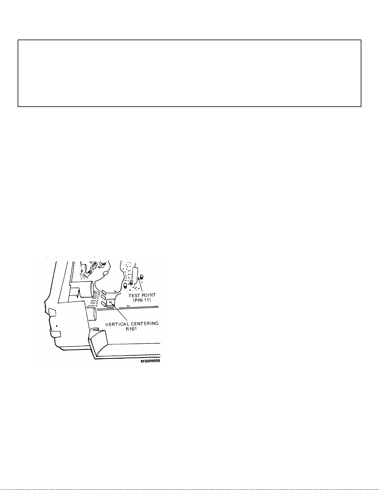
5. Adjust Vertical DC Centering
a.Connect the DC voltmeter between pin 11 of
U105 (positive meter lead to pin 11) and ground (see
Fig. 4-3).
b.Adjust CH 1 Vertical POS control for a 0 volt
meter reading.
c.CHECK-Trace should be within approximately
0.4 division of graticule center.
d.ADJUST-Vertical Centering, R101 (see Fig. 4-3)
to position the trace to the center horizontal graticule line.
e.Disconnect all test equipment.
6.Probe Tip-to-BNC Adapter
7.50-Ohm BNC Termination
8.10X 50-Ohm Attenuator
9.Three-inch Screwdriver
10.Low-Capacitance Screwdriver
6. Adjust CH 1 STEP ATTENuator BALance
a.Rotate the CH 1 VOLTS/D)V switch from 50 m
to 1 m.
b.CHECK-The CRT display for 0.1 division or less
of trace shift between adjacent switch positions when
rotating the VOLTS/DIV switch from 50 m to 1 m.
c.ADJUST-CH 1 STEP ATTEN BAL, R415
(located on the side panel) for minimum trace shift when
rotating the CH 1 VOLTS/DIV switch from 50 m to 1 m.
7. Adjust CH 2 STEP ATTENuator BALance
a.Turn the CH 1 POS control to the OFF detent
and the CH 2 POS control to midrange.
b.Rotate the CH 2 VOLTS/DIV switch from 50 m to
1 m.
c.CHECK-The CRT display for 0.1 division or less
of trace shift between adjacent switch positions when
rotating the VOLTS/DIV switch from 50 m to 1 m.
d.ADJUST-CH 2 STEP ATTEN BAL, R315
(located on the side panel) for minimum trace shift
rotating the CH 2 VOLTS/DIV switch from 50 m to 1 m.
Figure 4-3. Location of Vertical Centering adjustment and
test point.
8. Adjust VERTical GAIN
a.Set the CH 2 VOLTS/DIV switch to 5 m.
b.Connect the CH 2 probe tip to the output of the
Standard Amplitude Calibrator via a probe tip-to-BNC
adapter.
c.Set the Standard Amplitude Calibrator for a 20
millivolts output signal.
d.CHECK-The CRT display for four divisions of
deflection within 0.2 division.
e.ADJUST-VERT GAIN, R470 (located on the side
panel) for exactly four divisions of deflection.
4-5
Page 25

TM 9-6625-646-14&P
9. Check CH 2 VARiable VOLTS/DIV Range
a.Rotate the CH 2 VOLTS/DIV VAR control fully
clockwise.
b.CHECK-The CRT display for 1.6 divisions or
less of deflection. 1.6 divisions of deflection indicates a
VARiable VOLTS/DIV range of at least 2.5: 1.
c.Set the VARiable VOLTS/D IV control to CAL.
10. Check CH 2 VOLTS/DIV Accuracy
a.CHECK-Using the CH 2 VOLTS/DIV switch and
Standard Amplitude Calibrator settings given in Table 43, check that the deflection factor acc uracy for CH 2 is
within 5% at each position.
TABLE 4-3.
Vertical Deflection Accuracy
VOLTS/DIVStandard Vertical Maximum
Switch AmplitudeDeflection Error For
Setting Calibrator in Ù5% Accuracy
Output Divisions
1 m 5 millivolts 5 Ù0.25 division
2 m 10 millivolts 5
5 m 20 millivolts 4 Previously set in
10 m 50 millivolts 5
20 m 0.1 volt 5
50 m 0.2 volt 4
.1 0.5 volt 5
.2 1 volt 5
.5 2 volts 4
1 5 volts 5
2 10 volts 5
5 20 volts 4
10 50 volts 5
20 100 volts 5
50 100 volts 2
Ù0.25 division
step 8.
Ù0.25 division
Ù0.25 division
Ù0.2 division
Ù0.25 division
Ù0.25 division
Ù0.2 division
Ù0.25 division
Ù0.25 division
Ù0.2 division
Ù0.25 division
Ù0.25 division
Ù0.1 division
b.Disconnect the CH 2 probe tip from the Standard
Amplitude Calibrator.
a.Turn CH 2 POS to the OFF detent and the CH 1
POS to midrange.
b.Connect the CH 1 probe tip to the output of the
Standard Amplitude Calibrator via a probe tip-to-BNC
adapter.
c.CHECK-Using the CH 1 VOLTS/DIV switch and
Standard Amplitude Calibrator settings given in Table 43, that the deflection factor accuracy of CH 1 at each
position is within 5%.
d.Set the Standard Amplitude Calibrator for a 20
millivolts output signal.
e.Set the CH 1 VOLTS/DIV switch to 5 m.
f.Rotate the CH 1 VARiable VOLTS/DIV control
fully clockwise.
g.CHECK-The CRT display for 1.6 divisions or
less of deflection. 1.6 divisions of deflection indicates a
VARiable VOLTS/DIV range of at least 2.5: 1.
h.Set the VARiable VOLTS/DIV control to CAL.
12. Adjust CH 1 VOLTS/DIV Switch Compen-sation
a.Set the CH 1 VOLTS/DIV switch to 0.1 V.
b.Connect the CH 1 probe tip to the high amplitude
output of the Type 106 Square-Wave generator via a
GR-to-BNC female adapter, a 50-ohm BNC ter mination,
and a probe tip-to-BNC adapter.
c.Adjust the Square-Wave generator for a fourdivision display of a one kilohertz square wave.
d.Adjust the Triggering controls for a stable
display.
e.CHECK-The CRT display for flat-top waveform
with no more than +0.2 division, -0.1 division, or a total of
0.2 division of aberration.
NOTE
If C307, C308, C309, C407, C408, or
C409 require adjustment, it will be
necessary to remove the instrument
side panel from the Input Board.
Refer to the Disassembly Instructions
for removal procedure.
11. Check CH 1 VOLTS/DIV Accuracy and VARiable
VOLTS/DIV Range
4-6
Page 26

f.ADJUST-C407 (see Fig. 4-4) for no more than
+0.2 division, -0.1 division, or a total of 0.2 division of
aberration. (Use a low-capacitance screwdriver.)
g.Set the CH 1 VOLTS/DIV switch to 1 and adjust
the Square-Wave generator for a four-division display.
h.CHECK-The CRT display for flat-top waveform
with no more than +0.2 division, -0.1 division, or a total of
0.2 division of aberration.
i.ADJUST-C408 (see Fig. 4-4) for no more than
+0.2 division, -0.1 division, or a total of 0.2 division of
aberration.
j.Set the VOLTS/DIV switch to 10, remove the 50ohm BNC termination from the test s etup, and adjust the
Square-Wave generator for a four-division display.
k.CHECK-The CRT display for a flat-top waveform
with no more than +0.2 division, -0.1 division, or a total of
0.2 division of aberration.
I.ADJUST-C409 (see Fig. 4-4) for no more than
+0.2 division, -0.1 division, or a total of 0.2 division of
aberration.
m.Disconnect CH 1 probe tip from the test setup.
Figure 4-4. Location of attenuator compensation
capacitors.
TM 9-6625-646-14&P
13. Adjust CH 2 VOLTS/DIV Switch Compensation
a.Turn CH 1 POS control to the OFF detent and
turn CH 2 POS control to midrange.
b.Set the CH 2 VOLTS/DIV switch to 0.1 V/div.
c.Connect the CH 2 probe tip to the high amplitude
output of the Type 106 Square-Wave generator via a
GR-to-BNC female adapter, a 50-ohm BNC ter mination,
and a probe tip-to-BNC adapter.
d.Adjust the Square-Wave generator for a fourdivision display of a one-kilohertz square wave.
e.CHECK-The CRT display for flat-top waveform
with no more than +0.2 division, -0.1 division, or a total of
0.2 division of aberration.
f.ADJUST-C307 (see Fig. 4-4) for no more than
+0.2 division, -0.1 division, or a total of 0.2 division of
aberration.
g.Set the CH 2 VOLTS/DIV switch to 1 and adjust
the Square-Wave generator for a four-division display.
h.CHECK-The CRT display for a flat-top waveform
with no more than +0.2 division, -0.1 division, or a total of
0.2 division of aberration.
i.ADJUST-C308 (see Fig. 4-4) for no more than
+0.2 division, -0.1 division, or a total of 0.2 division of
aberration.
j.Set the CH 2 VOLTS/DIV switch to 10, remove
the 50-ohm BNC termination from the test setup, and
adjust the Square-Wave generator for a four-division
display.
k.CHECK-The CRT display for a flat-top waveform
with no more than +0.2 division, -0.1 division, or a total of
0.2 division of aberration.
I.ADJUST-C309 (see Fig. 4-4) for no more than
+0.2 division, -0.1 division, or a total of 0.2 division of
aberration.
m.Disconnect all test equipment, and re-install the
instrument side panel.
4-7
Page 27

14. Check CH 2 Vertical Amplifier Bandwidth
a. Set the CH 2 VOLTS/DIV switch to 1 m.
b. Connect the CH 2 probe tip to the output of the
Low Frequency Constant-Amplitude signal generator via
a 50-ohm BNC 10X attenuator and a probe tip-to-BNC
adapter.
c. Adjust the signal generator for a six-division
display for a one-kilohertz signal.
d. W ithout adjusting the output am plitude, increase
the output frequency until the display is reduced in
amplitude to 4.2 divisions.
e. CHECK-T he signal generator output must be at
least 100 kilohertz.
f. Set the VOLT S/DIV switch to 2m and adjust the
signal generator for a six-division display of a onekilohertz signal.
g. W ithout adjusting the output am plitude, increase
the output frequency until the display is reduced in
amplitude to 4.2 divisions.
h. CHECK-T he signal generator output must be at
least 200 kilohertz.
i. Set the VOLTS/DIV switch to 5m and adjust
the signal generator for a six-division display of a onekilohertz signal.
TM 9-6625-646-14&P
j. W ithout adjus ting the output amplitude, increase
the output frequency until the display is reduced in
amplitude to 4.2 divisions.
k. CHECK-The signal generator output frequency
must be at least 400 kilohertz.
I. Set the VOLTS/DIV switch to 10 m and adjust
the signal generator for a six-division display of a onekilohertz signal.
m. Without adjusting the output am plitude, increase
the output frequency until the display is reduced in
amplitude to 4.2 divisions.
n. CHECK-The signal generator output frequency
must be at least 500 kilohertz.
o. Remove CH 2 probe tip from the test setup.
15. Check CH 1 Vertical Amplifier Bandwidth
a. Connect CH 1 probe tip to the test setup.
b. Turn CH 2 POS to the OFF detent and CH 1
POS to midrange.
c. Set the CH 1 VOLTS/DIV switch to 1 m.
d. Repeat steps 14-c through 14-n.
4-8
Page 28

TRIGGER CIRCUIT ADJUSTMENT
Equipment Required
1. Low Frequency Signal Generator
2. 42-inch 50-Ohm BNC Cable
3. BNC-T Connector
Control Settings
Preset instrument controls to the settings given under
Preliminary Control Settings except as follows:
INTENSITY Visible Display
SEC/DIV .1 m
CH 1 INPUT COUPLING DC
CH 1 POS OFF
CH 2 POS Midrange
Trigger SOURCE CH 2
16. Adjust AUTO PRESET
a. Connect the CH 2 probe tip to the output of the
Low Frequency signal generator via a BNC-T connector
and a probe tip-to-BNC adapter.
b. Adjust the signal generator for a 0.2 division
display of a five-kilohertz signal.
c. CHECK-For a stable display.
d. ADJUST -AUTO PRESET, R375 (located on the
side panel) for a stable display.
17. Check Trigger Circuit Operation
TM 9-6625-646-14&P
4. BNC to Banana Plug Adapter
5. Three-inch Screwdriver
6. Probe tip-to-BNC Adapter
a. Set the CH 2 VOLTS/DIV switch to 1 V.
b. Adjust the signal generator for a one-division
display of a 500 kilohertz signal.
c. Set the CH 2 VOLTS/DIV switch to 5 V.
d. CHECK-A stable display can be obtained by
adjusting the LEVEL/SLOPE control to trigger on both
the positive-going and negative-going slopes of the
displayed waveform.
e. Return the LEVEL/SLOPE control to the AUTO
PRESET detent.
f. Set the Trigger SOURCE switch to COMP.
g. CHECK-A stable display can be obtained by
adjusting the LEVEL/SLOPE control to trigger on both
the positive-going and negative-going slopes of the
displayed waveform.
h. Set the Tr igger SOURCE switch to EXT and the
LEVEL/SLOPE control to the AUTO PRESET detent.
i. Connect the unused output of the BNC-T
connector to the 212 EXT T RIG input via a 42-inc h BNC
cable and a BNC-to-banana plug adapter.
j. CHECK-A stable display can be obtained by
adjusting the LEVEL/SLOPE control to trigger on both
the positive-going and negative-going slopes of the
displayed waveform.
4-9
Page 29

1.Standard Amplitude Calibrator
2.Time-Mark Generator
3.DC Voltmeter
4.42-inch 50-ohm BNC Cable
TM 9-6625-646-14&P
HORIZONTAL SYSTEM ADJUSTMENT
Equipment Required
5.BNC-to-Banana Plug Adapter
6.Probe Tip-to-BNC Adapter
7.Three-inch Screwdriver
Control Settings
Preset instrument controls to the settings given under
Preliminary Control Settings except as follows:
INTENSITY Visible Display
SEC/DIV X-Y
CH 2 POS Midrange
18. Adjust Horizontal Centering
a.Align dot to graticule center using HORIZ POS
and CH 2 VERT POS control.
b.Connect the DC voltmeter between pin 5 of
U105 (positive meter lead to pin 5) and ground. (See
Fig. 4-5 for test point and adjustment location.)
c.CHECK-For a reading of 0 volts, +0.2 volt.
d.ADJUST-Horizontal Centering, R366 for a meter
reading of 0 volts +0.1 V.
19. Adjust HORIZontal GAIN
a.Connect the CH 1 probe tip to the output of the
Standard Amplitude Calibrator via a probe tip-to-BNC
adapter.
b.Set the Standard Amplitude Calibrator for a 20
millivolts output.
c.Set CH 1 INPUT COUPLING switch to DC.
d.CHECK-The CRT display for two dots
separated horizontally by four divisions, +0.2 division.
e.ADJUST-Horiz Gain, R475 (located on the side
panel) for four divisions of deflection between dots.
f.Disconnect all test equipment.
20. Adjust SWEEP CALibration
a.Connect the CH 1 probe tip to the output of the
Time-Mark generator via a probe tip-to-BNC adapter.
b.Set the SEC/DIV switch to 1 m and the TimeMark generator for 1 millisecond markers.
c.Set CH 2 POS to the OFF detent.
d.Adjust the CH 1 VOLTS/DIV switch for a display
approximately three divisions in amplitude.
Figure 4-5. Location of Horizontal Centering adjustment
and test point.
4-10
Page 30

TM 9-6625-646-14&P
e. CHECK-T he CRT display for one time mark per
division. With the second time mark aligned with the
second vertical graticule line, the tenth tim e mark should
align with the tenth vertical graticule line within 0.4
division.
f. ADJUST-SWEEP CAL, R370 (located on the
side panel) for exactly eight divisions of deflection
between the second and tenth time marks.
21. Check Horizontal Magnification Range
a. Rotate the HOR IZ MAG control fully clockwise.
b. CHECK-The CRT display for at least five
divisions between adjacent time marks. Five-division
spacing indicates a HORIZ MAG control range of at least
5:1.
c. Return the HORIZ MAG control to the CAL
detent.
22. Check SEC/DIV Accuracy
a. CHECK-Apply the appropriate time marks and
check each position of the SEC/DIV switch for proper
timing over the center eight division portion of each
sweep, within 0.4 division.
4-11
Page 31

SECTION 5
TROUBLESHOOTING AIDS
TM 9-6625-646-14&P
TROUBLESHOOTING AIDS
Complete circuit diagrams are given in the rear of this
manual. The component number and electrical value of
each component in this instrument are shown on the
diagrams along with important voltages. The portions of
the circuit mounted on circuit boards are enclosed with
blue lines.
Figure 3-2 shows the location of the circuit boards
within the instrument along with the assembly (A)
numbers. The assembly numbers are also us ed on the
diagrams to aid in locating the boards. Pictures of the
circuit boards are shown in the Diagrams section, on the
back of the page opposite the circuit diagram, to aid
cross-referencing between the diagrams and the circuit
board pictures. Each electrical component on the boards
is identified by its circuit number as well as the
interconnecting wires and/or connectors.
Component Color Coding
The resistors used in this instrument are either
composition resistors or precision resistors. The
resistance values are color-coded on the components
with EIA color-code (some precision r esistors may have
the value printed on the body). The color-code is read
starting with the stripe nearest the end of the resistor.
Composition resistors have four stripes which c onsist of
two significant figures, a multiplier, and a tolerance value
(see Fig. 5-1). Precision resistors have five stripes
consisting of three significant figures, a multiplier, and a
tolerance value.
The capacitance values of common disc capacitors
and small tubular electrolytics are marked in mic rofarads
on the side of the component body. The molded
electrolytic capacitors ar e color-coded in picofarads (see
Fig. 5-1).
The cathode end of each glass-encased diode is
indicated by a stripe, a series of stripes, or a dot.
Figure 5-1. Color code for resistors, ceramic capacitors, and dipped tantalum electrolytic capacitors.
5-1
Page 32

Figure 5-2. Lead configuration of semiconductors used in this instrument.
TM 9-6625-646-14&P
Semiconductor Lead Configuration
Figure 5-2 shows the lead configurations of the
semiconductors used in this instrument.
Troubleshooting Equipment
The majority of troubleshooting to be done on the 212
can be accomplished with a 20, 000 ohms/volt VOM
such as a Triplett Model 630-NA or a Simpson Model
262. Use a dynamic transistor tester such as a
TEKTRONIX Type 576 Transistor-Curve Trac er to c heck
the semiconductor devices used in the 212. To check
waveform(s) in this instrument, use a test oscilloscope
with a DC to 500 kilohertz frequency response and one
millivolt to 50 volts/division deflection factor.
5-2
Page 33

SECTION 6
CIRCUIT DESCRIPTION
TM 9-6625-646-14&P
The following circuit description begins with a
discussion of the instrument using the block diagram
located in the Diagrams section at the rear of this
manual. Then each circuit is described in detail, using
detailed diagrams where necessary to show the
interconnections between the stages in each major
circuit and the relationship of the side-panel controls to
the individual stages. In addition to the block diagram,
complete schematics are given in the Diagrams section.
Block Diagram
Signals to be displayed on the CRT are applied to the
tips of the signal probes. The signals are then amplif ied
by the appropriate channel Input Amplifier circuit,
consisting of a two-section source-follower stage and two
feedback amplifiers. The Input Amplifier circuits also
contain the vertical deflection, position (with channel onOFF), input coupling, variable attenuation, and balance
controls.
The Trigger Generator circuit initiates the sweep
signal produced by the Sweep Generator. The input
signal to the Trigger Generator can be select ed internally
either from the capacitively coupled CH 2 Input Am plifier
signal, or from the direc tly coupled COMPosite signal of
the Feedback Amplifier. The Trigger Generator input
signal can also be selected from the external signal
applied to the EXT TRIG jack. The Trigger Generator
circuit contains coupling and sourc e controls in addition
to a combination level/slope control.
The Sweep Generator circuit produces a linear
sawtooth output signal when initiated by the Trigger
Generator circuit. The slope of the sawtooth signal is
controlled by the SEC/DIV switch. The Sweep Generator
circuit also produces an unblanking gate signal
coincident with the sawtooth waveform. This gate s ignal
unblanks the CRT to permit display presentation.
The output of U370 is amplified by the Horizontal
Amplifier circuit to produce the correct horizontal
deflection for the CRT for all positions of the SEC/DIV
switch. The Horizontal Amplifier contains a variable
magnifier to increase the sweep rate up to at least a
maximum of five times in any position of the SEC/DIV
switch.
The Power Supply and CRT circuits provide all the
voltages necessary for operation of this instrument.
Circuit Operation
In the following description of the electrical operation
and relationship of the circuits in the 212, circuitry
commonly used by TEKTRONIX is only briefly explained.
If more information is desired on the commonly used
circuits, refer to the following textbooks:
Phillip Cutler, "Semiconductor Circuit Analysis",
McGraw-Hill, New York, 1964.
Lloyd P. Hunter (Ed.), "Handbook of Semiconductor
Electronics", second edition, McGraw-Hill, New York,
1962.
Jacob Millman and Herbert Taub, "Pulse, Digital, and
Switching Waveforms", McGraw-Hill, New York, 1965.
6-1
Page 34

TM 9-6625-646-14&P
Vertical Input Amplifiers
Input signals for vertical deflection of the CRT of the
212 are applied to the tips of the attached probes. Each
Input Amplifier provides control of input coupling, variable
attenuation, vertical deflection factor, balance, and
vertical position (with channel on-OFF) for the
appropriate channel. Figure 6-1 shows a detailed block
diagram of the Vertical Input Amplifier circuit. A
schematic of this circuit is shown on diagram 1.
Input signals applied to the tips of the probes are
connected to the appropriate Attenuation Stage through
the INPUT COUPLING switches (S305 and S405) . The
deflection factor in each channel is determined by the
VOLTS/DIV switch (S310 or S410). In all positions of the
VOLTS/DIV switches below .1 V/DIV, the correct
deflection factor is achieved by changing the gain of
Feedback Amplifiers U320-A and U320-B. In switch
positions .1 V/DIV and up, precision attenuators are used
(in addition to changing the gain of U320-A and U320-B)
to achieve the correct deflection factors. When the
VOLTS/DIV VAR control is rotated, the signal is
attenuated across R320 or R420. This offers variable
(uncalibrated) deflection factors between the calibrated
settings of the VOLTS/DIV switch. The STEP ATTEN
BALance adjustments (R315 and R417) control the tr ace
shift when switching between deflection factors.
The 212 can be operated single trace by turning
either vertical POSition control to the OFF detent; this
disables that channel in the last feedback stage of the
Input Amplifier through the operation of the Vertical
Mode Multivibrator U440. The CH 2 trigger signal is
present regardless of the CH 2 POS control setting. In
the dual-trace mode, the instrument will automatically
chop or alternate, depending upon the sweep rate.
Figure 6-1. Vertical input amplifiers detailed block diagram.
6-2
Page 35

TM 9-6625-646-14&P
Vertical and Horizontal Output Amplifiers
The Vertical and Horizontal Output Amplifiers provide
the final amplification for the deflection signals. Figure 62 shows a detailed block diagram of these Output
Amplifiers. A schematic of these c ircuits is on diagram
2.
Both amplifiers contain the same basic circuitry. The
single-ended input signals are applied to paraphase
amplifiers, U105-A and U105-B, to convert the signal into
push-pull output signals. The Vertical Paraphase
Amplifier stage contains the VERT GAIN adjustment
(R470) that sets the over-all gain of the ver tical system,
and a Vertical Centering adjustment (R101) to set DC
centering. The Horizontal Paraphase Amplifier stage
contains the HORIZ GAIN adjustment (R475), the
HORIZ MAG control (R476), and the Horizontal POSition
control (R480). The output signals from the Paraphase
Amplifiers receive final amplification in the c ommon bas e
Output Amplifier stages.
Figure 6-2. Vertical and Horizontal output amplifiers detailed block diagram.
6-3
Page 36

TM 9-6625-646-14&P
Trigger/Sweep Generator
Integrated circuit U370 is a combination
Trigger/Sweep Generator. The Trigger portion derives
trigger signals internally, either from the capacitively
coupled CH 2 Vertical Input Amplifier, or from the direc tly
coupled COMPosite signal from the input of the Vertic al
Output Amplifier. The Trigger portion can also select
signals from an external signal applied to the EXT TRIG
banana jack. Controls are provided in this circuit to
select trigger level, slope, and source. Figure 6- 3 shows
a detailed block diagram of the Tr igger/Sweep G enerator
circuit. A schematic of this circuit is on diagram 2.
The Sweep Generator portion of U370 serves a
multiple purpose. In all positions of the SEC/DIV switch
except X-Y, the Sweep Generator is an integrator, which
generates a linear sawtooth voltage waveform. The
slope of the sawtooth voltage is controlled by the setting
of the SEC/DIV switch. U370 also produces an
unblanking gate signal coincident with the sawtooth
waveform. This gate signal is amplified by Unblanking
Amplifier Q134 and applied to the CRT to unblank the
CRT during sweep presentation. In addition, the Sweep
Generator supplies the clock pulses to the Vertical Mode
Multivibrator for alternate switching between channels.
In the X-Y position, the Sweep Generator section
becomes a feedback amplifier to amplify the signal
applied to the probe tip of CH 1.
Figure 6-3. Trigger/Sweep Generator detailed block diagram.
6-4
Page 37

TM 9-6625-646-14&P
Power Supply
The Power Supply provides the power necessary to
operate this instrument or, if the instrument is turned off,
to recharge the batteries. Figure 6-4 shows a detailed
block diagram of this circuit. A schematic of this circuit is
shown on diagram 4.
When the instrument is connected to a power line the
AC power is capacitively coupled to the Power Rectifier.
The rectified DC is used to either run the instrument or
recharge the internal batteries. The batteries act as a
large filter capacitor for the Input Rectifier in the AC line
mode of TM 9-6625-646-14&P operation. When the
instrument is not connected to a power line, operating
power is provided by the batteries. The POWER
(BATTERY) indicator, light emitting diode DS310, is
illuminated when the 212 is operating from line voltage or
adequately charged batteries. When about 10 minutes
of operating time remains, the battery charge drops to a
point where DS310 will extinguish. The Discharge
Protection circuit (0231, Q235) prevents the Converter
Multivibrator (Q242, Q249) from func tioning, and thereby
overdischarging the ’batteries, when the charge level of
the batteries falls below approximately 10 volts. The
Converter Multivibrator changes DC into AC, which is
applied across T250 and then rectified into the
appropriate DC voltages in the Rectifier circuit.
Figure 6-4. Power Supply detailed block diagram.
6-5
Page 38

TM 9-6625-646-14&P
CRT Circuit
The CRT circuit provides the high voltage and contr ol
circuits necessary for oper ation of the cathode-ray tube
(CRT). Figure 6-5 shows a detailed block diagram of the
CRT circuit. A schematic of this circuit is given on
diagram 3.
Rectifiers CR261 through CR268 provide the negative
accelerating potential for the CRT. Voltage output is
approximately -1000 volts at the CRT cathode. Filament
voltage for the CRT is provided by a spearate winding of
the power transformer. Display intensity and focus are
controlled by R395 and R398 respectively. The Trace
Rotation adjustment controls the current through L300
and affects both the vertical and horizontal alignment of
the CRT beam.
Figure 6-5. CRT Circuit detailed block diagram.
6-6
Page 39

SECTION 7
CORRECTIVE MAINTENANCE
TM 9-6625-646-14&P
Obtaining Replacement Parts
Standard Parts. All electrical and mechanical part
replacements for the 212 c an be obtained through your
local TEKTRON IX Field Office or representative.
However, many of the standard electronic components
can be obtained locally in less time than is required to
order them from Tektronix, Inc. Before purchasing or
ordering replacement parts, c hec k the parts list for value,
tolerance, rating, and description.
NOTE
When selecting replacement parts, it
is important to remember that the
physical size and shape of a
component may affect its
performance in the instrument. All
replacement parts should be direct
replacements unless it is known that
a different component will not
adversely affect the instruments
performance.
Special Parts. In addition to the standard electronic
components, som e special components are used in the
212. These components ar e manufactured or selected
by Tektronix, Inc., to meet specific performance
requirements, or are m anufactured for Tektronix, Inc . in
accordance with our specifications. Most of the
mechanical parts used in this instrument have been
manufactured by Tektr onix, Inc . O rder all s pecial parts
directly from your local TEKTRONIX Field Office or
representative.
Ordering Parts. When ordering replacement
parts from Tektronix, Inc., include the following
information:
1. Instrument type.
2. Instrument serial number.
3. A description of the part (if electrical, include
circuit number).
4. TEKTRONIX Part Number.
Circuit Board Replacement. If a circuit board is
damaged beyond repair, the entire assembly including all
soldered-on components can be replaced. Part numbers
are given in the Mechanical Parts List f or the com pletely
wired board.
Semiconductor Replacement. Semiconductors
should not be replaced unless actually defective. If
removed from their sockets during routine m aintenance,
return them to their original sockets. Unnecessary
replacement of semiconductors may affect the
calibration of the instrument. W hen semiconduc tors are
replaced, check the operation of that part of the
instrument which may be affected.
Replacement semiconductors should be of the
original type or a direct replacement. Figure 5-2 shows
the lead configurations of the semiconductors used in
this instrument. Som e plastic case transistors have lead
configurations which do not agree with those shown
here. If a replacement transistor is made by a
manufacturer other than that of the or iginal, c heck the
replacement manufacturer’s basing diagram for correct
basing. All transistor sock ets in the 212 are wired for the
basing used for metal-cased transistors.
When re-inserting an integrated circuit, key the
socket’s index with that of the integrated circuit’s. Failure
to do so can result in damaged components.
Power Supply Capacitors. When operating the
Instrument on power lines other than 115 VAC 60 Hz, It
is necessary to change the electrical value of four
capacitors (C204, C215, C210, and C212) in the
instruments power input circuitry. Refer to Table 7-1 f or
the correct values of capacitance for three of the more
commonly used line voltage/line frequency combinations.
NOTE
Power line for this instrument must
be sinusoidal.
Component Replacement
WARNING
Disconnect the instrument from any
power source before replacing
components.
7-1
Page 40

TM 9-6625-646-14&P
TABLE 7-1.
Power Supply Capacitors
Power Capacitor Values
Line C210 C212 C204 &C215
110 to 1.7 µf, +10% 3.3 µf, +10%, No change
126 VAC 200 V DC 200 V DC
58 to TEKTRONIX TEKTRONIX
62 Hz Part No. Part No.
285-0924-00 285-0925-00
90 to 2 µf , +10%, 4.0 µf, +10%, No change
110 VAC 200 V DC 200 V DC
48 to TEKTRONIX TEKTRONIX
52 Hz Part No. Part No.
(Option 2) 285-0934-00 285-0935-00
220 to 1 µf, +10%, 2.0 µf, +10%, .001 µf,
250 VAC 400 V DC 400 V DC 3 k V DC
48 to TEKTRONIX TEKTRONIX TEKTRONIX
52 Hz Part No. Part No. Part No.
(Option 1) 285-0932-00 285-0933-00 283-0279-00
If the instrument is to be operated on some line
voltage/line frequency combination other than one of the
above three examples, refer to Fig. 7-1 and Fig. 7-2 to
select the correct values of capacitance for C210 and
C212. For example, if the instrument is to be oper ated
on a 60 hertz line that will vary in voltage from 210 VAC
to 230 VAC, refer to Fig. 7-2. Trace across the graph on
the line representing 210 VAC to the point where that line
crosses the first curve. This point represents the
minimum values of capacitance that can be used for
correct operation. Now trace across the graph on the
line representing 230 VAC to the point where that line
crosses the second curve. This point represents the
maximum values of capacitance that can be used for
correct operation. Read off the numbers dir ectly under
these points at the bottom of the graph to find the value
of capacitance required for C210. Read off the number s
directly above these points for the value of capacitance
required for C212. Thus, C210 can be a value between
µf and 0.92 µf and C212 can be a value between
0.75
µf and 1.87 µf. The voltage ratings of these
1.54
capacitors should be at least 1.414 times the RMS value
of the applied line voltage.
Figure 7-1. Selecting C210 and C212 capacitance values for 48 to 52 Hz operation.
7-2
Page 41

TM 9-6625-646-14&P
When replacing C210 and C212, be certain the foam
pad is under the replacement capacitor.
Rotary Switches. Individual parts of the VOLTS/DIV
and SEC/DIV rotary switches are replaceable. Refer to
the Parts List for the applicable part numbers for
replacement parts.
Selectable Components. Resistor R388 value is
selected for a switching unblanked trace height of no
more than 1.5 divisions for each channel and minimum
intensity change when changing sweep speed from 5 ms
to 2 ms. The value of R388 is selected from a range of
270, 300, or 330 ohms as follows:
1. Install a 270 ohm resistor for R388, turn the
212 on, set SEC/DIV to .5 s, and set INTENSITY to
maximum (fully clockwise).
2.The traces will show as dots. Set CH 1 POS to
place the CH 1 dot to the top horizontal graticule line and
set CH 2 POS to place the CH 2 dot to the bottom
horiztontal graticule line.
3.Check that no more than 1.5 divisions of
unblanked trace extends vertically from each dot.
4.If each unblanked trace exceeds 1.5 vertical
divisions, turn off the 212, install the next larger size for
R388, recheck and repeat steps 2 through 4 until
unblanked traces are no more than 1.5 divisions high
while maintaining minimum intensity change when
switching sweep speed from 5 ms to 2 ms.
Figure 7-2. Selecting C210 and C212 capacitance values for 58 to 62 Hz operation.
7-3
Page 42

Repackaging For Shipment
If the Tektronix instrument is to be shipped to a
Tektronix Service Center for service or repair, attach a
tag showing: owner (with address) and the name of an
individual at your firm that can be contacted. Include
complete instrument s erial number and a description of
the service required.
Save and re-use the package in which your
instrument was shipped. If the original pack aging is unfit
for use or not available, repackage the instrument as
follows:
TM 9-6625-646-14&P
Surround the instrument with polyethylene sheeting to
protect the finish of the instum ent. Obtain a carton of
corrugated cardboard of the correct carton strength
and having inside dimensions of no less than six
inches more than the instrument dimenstions.
Cushion the instrument by tightly packing three inches
of dunnage or urethane foam between carton and
instrument, on all sides. Seal carton with shipping
tape or industrial stapler.
The carton test strength for your instrument is 200
pounds.
7-4
Page 43

TM 9-6625-646-14&P
SECTION 8
PARTS LISTS, DIAGRAMS AND
CIRCUIT BOARD ILLUSTRATIONS
Symbols and Reference Designators
Electrical components shown on the diagrams are in the following units unless noted otherwise:
Capacitors = Values one or greater are in picofarads (pF).
Values less than one are in microfarads (µF).
Resistors = Ohms (Ω)
Symbols used on the diagrams are based on USA Standard Y32.2-1967.
Logic symbology is based on MIL-STD-806B in terms of positive logic. Logic symbols depict the logic function per form ed
and may differ from the manufacturer’s data.
The following special symbols are used on the diagrams:
The following prefix letters are used as reference designators to identify components or assemblies on the diagrams.
A Assembly, separable or repairable (circuit board, etc.) LR Inductor/resistor combination
AT Attenuator, fixed or variable M Meter
B Motor Q Transistor or silicon-controlled rectifier
BT Battery P Connector, movable portion
C Capacitor, fixed or variable R Resistor, fixed or variable
CR Diode, signal or rectifier RT Thermistor
DL Delay line S Switch
DS Indicating device (lamp) T Transformer
F Fuse TP Test point
FL Filter U Assembly, inseparable or non-repairable
H Heat dissipating device (heat sink, heat radiator, etc.) (integrated circuit, etc.)
HR Heater V Electron tube
J Connector, stationary portion VR Voltage regulator (zener diode, etc.)
K Relay Y Crystal
L Inductor, fixed or variable
8-1
Page 44

TM 9-6625-646-14&P
REPLACEABLE
ELECTRICAL PARTS
PARTS ORDERING INFORMATION
Replacement parts are available from or through your local Tektronix, inc. Field Office or representative.
Changes to Tektronix instruments are sometimes made to accom modate improved components as they become
available, and to give you the benefit of the latest circuit improvements developed in our engineering department It is
therefore important, when ordering parts, to include the following information in your order: Part number, instrument type or
number, serial number, and modification number if applicable.
If a part you have ordered has been replaced with a new or improved part, your local Tek tronix, Inc Field Off ice or
representative will contact you concerning any change in part number.
Change information, if any, is located at the rear of this manual.
SPECIAL NOTES AND SYMBOLS
X000 Part first added at this serial number
00X Part removed after this serial number
ITEM NAME
In the Parts List, an Item Name is separated from the desc ription by a colon (:). Because of space limitations, an
Item Name may sometimes appear as incomplete. For further Item Name identification, the U.S. Federal Cataloging
Handbook H6-1 can be utilized where possible.
ABBREVIATIONS
ACTR ACTUATOR PLSTC PLASTIC
ASSY ASSEMBLY QTZ QUARTZ
CAP CAPACITOR RECP RECEPTACLE
CER CERAMIC RES RESISTOR
CKT CIRCUIT RF RADIO FREQUENCY
COMP COMPOSITION SEL SELECTED
CONN CONNECTOR SEMICOND SEMICONDUCTOR
ELCTLT ELECTROLYTIC SENS SENSITIVE
ELEC ELECTRICAL VAR VARIABLE
INCAND INCANDESCENT WW WIREWOUND
LED LIGHT EMITT4NG DIODE XFMR TRANSFORMER
NONWIR NON WIREWOUND XTAL CRYSTAL
8-2
Page 45

TM 9-6625-646-14&P
CROSS INDEX-MFR. CODE NUMBER TO MANUFACTURER
Mfr. Code Manufacturer Address City, State, Zip
01121 ALLEN-BRADLEY COMPANY 1201 2ND STREET SOUTH MILWAUKEE, WI 53204
01295 TEXAS INSTRUMENTS, INC., SEMICONDUCTOR P O BOX 5012, 13500 N CENTRAL
02735 RCA CORPORATION, SOLID STATE DIVISION ROUTE 202 SOMERVILLE, NY 08876
03508 GENERAL ELECTRIC COMPANY, SEMI-CONDUCTOR
03888 KDI PYROFILM CORPORATION 60 S JEFFERSON ROAD WHIPPANY, NJ 07981
04099 CAPCO, INC. FORESIGHT INDUSTRIAL PARK,
04713 MOTOROLA, INC., SEMICONDUCTOR PROD. DIV. 5005 E MCDOWELL RD, PO BOX 20923 PHOENIX, AZ 85036
07263 FAIRCHILD SEMICONDUCTOR, A DIV. OF
14752 ELECTRO CUBE INC. 1710 S. DEL MAR AVE. SAN GABRIEL, CA 91776
15238 ITT SEMICONDUCTORS, A DIVISION OF INTER
27014 NATIONAL SEMICONDUCTOR CORP. 2900 SEMICONDUCTOR DR. SANTA CLARA, CA 95051
32997 BOURNS, INC., TRIMPOT PRODUCTS DIV. 1200 COLUMBIA AVE. RIVERSIDE, CA 92507
56289 SPRAGUE ELECTRIC CO. 87 MARSHALL ST. NORTH ADAMS, MA 01247
71450 CTS CORP. 905 N. WEST BLVD ELKHART, IN 46514
72982 ERIE TECHNOLOGICAL PRODUCTS, INC. 644 W. 12TH ST. ERIE, PA 16512
73138 BECKMAN INSTRUMENTS, INC., HELIPOT DIV. 2500 HARBOR BLVD. FULLERTON, CA 92634
75915 LITTELFUSE, INC. 800 E. NORTHWEST HWY DES PLAINES, IL 60016
76493 BELL INDUSTRIES, INC.,
79727 C-W INDUSTRIES 550 DAVISVILLE RD., P O BOX 96 WARMINISTER, PA 18974
80009 TEKTRONIX, INC. P O BOX 500 BEAVERTON, OR 97077
80031 ELECTRA-MIDLAND CORP., MEPCO DIV. 22 COLUMBIA ROAD MORRISTOWN, NJ 07960
84411 TRW ELECTRONIC COMPONENTS, TRW CAPACITORS 112 W. FIRST ST. OGALLALA, NE 69153
90201 MALLORY CAPACITOR CO., DIV. OF 3029 E. WASHINGTON STREET
GROUP EXPRESSWAY DALLAS, TX 75222
PRODUCTS DEPARTMENT ELECTRONICS PARK SYRACUSE, NY 13201
PO BOX 2164 GRAND JUNCTION, CO 81501
FAIRCHILD CAMERA AND INSTRUMENT CORP. 464 ELLIS STREET MOUNTAIN VIEW, CA 94042
NATIONAL TELEPHONE AND TELEGRAPH CORP. P.O. BOX 168, 500 BROADWAY LAWRENCE, MA 01841
MILLER, J. W., DIV. 19070 REYES AVE., P O BOX 5825 COMPTON, CA 90224
P. R. MALLORY AND CO., INC. P.O. BOX 372 INDIANAPOLIS, IN 46206
91637 DALE ELECTRONICS, INC. P.O. BOX 609 COLUMBUS, NE 68601
8-3
Page 46

TM 9-6625-646-14&P
Tektronix Serial/Model No. Mfr
Ckt No. Part No. Eff Dscont Name & Description Code Mfr Part Number
A1 670-2353-00 B010100 B056848 CKT BOARD ASSY:INPUT 80009 670-2353-00
A1 670-2353-02 B056849 B079999 CKT BOARD ASSY:INPUT 80009 670-2353-02
A1 670-2353-04 B080000 B089999 CKT BOARD ASSY:INPUT 80009 670-2353-04
A1 670-2353-06 B090000 CKT BOARD ASSY:INPUT 80009 670-2353-06
A2 670-1505-01 CKT BOARD ASSY:AMPLIFIER 80009 670-1505-01
A3 670-2405-00 B010100 B039999 CKT BOARD ASSY:POWER SUPPLY 80009 670-2405-00
A3 670-2405-11 B040000 CKT BOARD ASSY:POWER SUPPLY 80009 670-2405-11
A3 670-2405-21 CKT BOARD ASSY:POWER SUPPLY 80009 670-2405-21
A3 670-2405-31 CKT BOARD ASSY:POWER SUPPLY 80009 670-2405-31
BT216 146-0031-00 B010100 B056119 BATTERY ASSY:2 SETS OF 5 80009 146-0031-00
BT217 146-0031-00 B010100 B056119 BATTERY ASSY:2 SETS OF 5 80009 146-0031-00
BT216 146-0033-00 B056120 BATTERY ASSY:2 SETS’ OF 5 80009 146-0033-00
BT217 146-0033-00 B056120 BATTERY ASSY:2 SETS OF 5 80009 146-0033-00
C101 283-0111-00 CAP., FXD, CER DI:0.IUF, 20%, 50V 72982 8121-N088Z5U104M
C103 283-0111-00 CAP., FXD, CER DI:O.1UF, 20X, 50V 72982 8121-N088Z5U104M
C104 281-0591-00 B010100 B057908 CAP., FXD, CER DI:5600PF, 20%, 200V 72982 393001%5V0562Z
C104 283-0180-00 B057909 CAP., FXD, CER DI:5600PF, 20%, 200V 72982 8121N204 E 562M
C113 283-0111-00 CAP., FXD, CER DI:O.lUF, 20%, 50V 72982 8121-N088Z5U104M
C115 283-0111-00 CAP., FXD, CER DI:0.1UF, 20%, 50V 72982 8121-N088Z5U104M
----------------- (OPTION 1 ONLY)
----------------- (OPTION 2 ONLY)
}
(BT216, BT217 SEE MPL FOR SUB-PARTS.)
}
----------------- (BT216, BT217 SEE MPL FOR SUB-PARTS.)
C125 290-0524-00 CAP. , FXD, ELCTLT:4.7UF, 20%, 1OV 90201 TDC475MO10EL
C127 290-0524-00 CAP., FXD, ELCTLT:4.7UF, 20%, 1OV 90201 TDC475M01OEL
C129 290-0534-00 CAP., FXD, ELCTLT:1UF, 20%, 35V 56289 196D105X0035HA1
C145 290-0522-00 CAP., FXD, ELCTLT:IUF, 20%, 50V 56289 196D105X0050HA1
C150 281-0591-00 B010100 B057908 CAP., FXD, CER DI:5600PF, 20%, 200V 72982 393001%5V0562Z
C150 283-0180-00 B057909 CAP., FXD, CER DI:5600PF, 20%, 200V 72982 8121N204 E 562M
C153 281-0591-00 B010100 B057908 CAP., FXD, CER DI:5600PF, 20%, 200V 72982 393001%5V0562Z
C153 283-0180-00 B057909 CAP., FXD, CER DI:5600PF, 20%, 200V 72982 8121N204 E 562M
C204 283-0280-00 BO010100 B039999 CAP., FXD, CER DI:2200PF, lO%, 2000V 56289 562CBA202EH222KA
C204 283-0263-00 B040000 CAP., FXD, CER DI:0.0022UF, 20%, 3000V 56289 33C319
C204 283-0279-00 CAP., FXD, CER DI:0.OOlUF, 20%, 3000V 56289 55C153
C206 283-0057-00 B010100 B042499 CAP., FXD, CER DI:0.1UF, +80-20%, 200V 56289 274C10
C206 285-1065-00 B042500 CAP., FXD, PLSTC:O.O1UF, 20%, 600V 14752 230B1F103
C207 283-0057-00 B010100 B042499 CAP., FXD, CER DI:O.1UF, +80-20%, 200V 56289 274C10
C207 285-1065-00 B042500 CAP., FXD, PLSTC:0.O1UF, 20%, 600V 14752 230BIF103
C210 285-0924-00 CAP., FXD, PLSTC:1.7UF, 10%, 200V 04099 C703C175K
C210 285-0932-00 CAP., FXD, PLSTC:lUF, 10%, 400V 14752 A-1478
C210 285-0934-00 CAP., FXD, PLSTC:2.2UF, 10%, 200V 56289 430P238
C212 285-0925-00 CAP., FXD, PLSTC:3.3UF, 10%, 200V 84411 TEK121-33592
C212 285-0933-00 CAP., FXD, PLSTC:2UF, 10%, 400V 14752 A-1480
C212 285-0935-00 CAP., FXD, PLSTC:4.4UF, 10%, 200V 56289 430P179
----------------- (NOMINAL VALUE, SELECTED FOR LINE VOLTAGE
AND (FREQUENCY. SEE OPTION INFORMATION.)
----------------- (NOMINAL VALUE, SELECTED FOR LINE VOLTAGE
----------------- AND (FREQUENCY. SEE OPTION INFORMATION.)
----------------- (OPTION 1 ONLY)
----------------- (NOMINAL VALUE, SELECTED FOR LINE VOLTAGE
----------------- AND (FREQUENCY. SEE OPTION INFORMATION.)
----------------- (OPTION 1 ONLY)
----------------- (OPTION 2 ONLY)
----------------- (NOMINAL VALUE, SELECTED FOR LINE VOLTAGE
----------------- AND (FREQUENCY. SEE OPTION INFORMATION.)
----------------- (OPTION 1 ONLY)
----------------- (OPTION 2 ONLY)
8-4
Page 47

TM 9-6625-646-14&P
Tektronix Serial/Model No. Mfr
Ckt No. Part No. Eff Dscont Name & Description Code Mfr Part Number
C215 283-0280-00 B010100 B039999 CAP., FXD, CER DI:2200PF, 10%, 2000V 56289 562CBA202EH222KA
C215 283-0263-00 B040000 CAP., FXD, CER DI:0.0022UF, 20%, 3000V 56289 33C319
C215 283-0279-00 CAP., FXD, CER DI:0.001UF, 20%, 3000V 56289 55C153
C216 283-0068-00 CAP., FXD, CER DI:O.01UF, +100-0%, 500V 56289 19C241
C236 283-0001-00 CAP., FXD, CER DI:0.005UF, +100-0%, 500V 72982 831-559E502P
C238 290-0534-00 CAP., FXD, ELCTLT:lUF, 20%, 35V 56289 196D105X0035HA1
C239 290-0283-00 CAP., FXD, ELCTLT:0, .47UF, 10%, 35V 56289 162D474X9035BC2
C241 283-0028-00 CAP., FXD, CER DI:0.0022UF, 20%, 50V 56289 19C606
C247 290-0519-00 CAP., FXD, ELCTLT:10OUF, 20%, 20V 90201 TDC107M020WLD
C251 290-0535-01 CAP., FXD, ELCTLT:33UF, 20%, 10OV 56289 196D336X0010KA1
C253 290-0535-01 CAP., FXD, ELCTLT:33UF, 20%, 10V 56289 196D336X0010KAI
C256 290-0517-00 CAP., FXD, ELCTLT:6.8UF, 20%, 35V 56289 196D685X0035KA1
C257 283-0057-00 CAP., FXD, CER DI:O.1UtF, +80-20%, 200V 56289 274C10
C258 290-0517-00 CAP., FXD, ELCTLT:6.8UF, 20%, 35V 56289 196D685X0035KA1
C260 283-0068-00 CAP., FXD, CER DI:O.01UF, +100-0%, 500V 56289 19C241
C261 283-0177-00 CAP., FXD, CER DI:lUF, +80-20%, 25V 56289 273C5
C262 283-0068-00 CAP., FXD, CER DI:0.01UF, +100-0%, 500V 56289 19C241
C263 283-0068-00 CAP., FXD, CER DI:O.O1UF, +100-0%, 500V 56289 19C241
C264 283-0068-00 CAP., FXD, CER DI:O.01UF, +100-0%, 500V 56289 19C241
C265 283-0068-00 CAP., FXD, CER DT:0.01UF, +100-0%, 500V 56289 19C241
C266 283-0068-00 CAP., FXD, CER DI:O.OIUF, +100-0%, 500V 56289 19C241
C267 283-0068-00 CAP., FXD, CER DI:O.O1UF, +100-0%, 50OV 56289 19C241
C268 283-0068-00 CAP., FXD, CER DI:0.O1UF, +100-0%, 500V 56289 19C241
C269 283-0001-00 CAP., FXD, CER DI:0.005F, +100-0%, 500V 72982 831-559E502P
C273 283-0105-00 CAP., FXD, CER DI:O.O1UF, +80-20%, 2000V 56289 41C316
----------------- (NOMINAL VALUE, SELECTED FOR LINE VOLTAGE
----------------- AND (FREQUENCY. SEE OPTION INFORMATION.)
----------------- (NOMINAL VALUE, SELECTED FOR LINE VOLTAGE
----------------- AND (FREQUENCY. SEE OPTION INFORMATION.)
----------------- (OPTION 1 ONLY)
C301 285-0697-06 CAP., FXD, PLSTC:O.IUF, +5-15%, 600V 80009 285-0697-06
C306B
C306D 307-0307-00 NTWK, HYB CKT: 80009 307-0307-00
}
C306F ----------------- (FURNISHED AS A UNIT WITH R306A-F)
C307 281-0178-00 CAP., VAR, PLSTC:1-3.5PF, 500V 80031 2805D013R5BH02FO
C308 281-0178-00 CAP., VAR, PLSTC:1-3.SPF, 500V 80031 2805D013R5BH02FO
C309 281-0178-00 CAP., VAR, PLSTC:1-3.5PF, 500V 80031 2805D013R5BH02FO
C313 283-0000-00 CAP., FXD, CER DI:O.OOt1UF, +100-0%, 500V 72982 831-516E102P
C321 283-0168-00 CAP., FXD, CER DI:12PF, 5%, 1OOV 72982 8101B121COG0120J
C323 281-0613-00 B010100 B010167 CAP., FXD, CER DI:10PF, +/-1PF, 200V 72982 374001COG10OF
C323 281-0645-00 B010168 B053776 CAP., FXD, CER DI:8.2PF, +/-0.25PF, 500V 72982 374018COH0829C
C323 281-0645-00 B053777 CAP., FXD, CER DI:8.2PF’, +/-0.25PF, 500V 72982 374018COH0829C
C327 283-0111-00 CAP., FXD, CER DI:0.1UF, 20%, 50V 72982 8121-N088ZSU104l
C329 290-0530-00 CAP., FXD, ELCTLT:68UF, 20%, 6V 90201 TDC686M006NLF
C348 283-0084-00 CAP., FXD, CER DI:270PF, 5%, 100OV 72982 838-533B271J
C349 283-0076-00 CAP., FXD, CER DI:27PF, 1lO%, 500V 56289 40C287A2
C353 290-0524-00 CAP., FXD, ELCTLT:4.7UJF, 20%, 10V 90201 TDC475MOlOEL
C362
C363 295-0144-00 CAP SET, MATCHED:1UF, O.OO1UF, MATCHED 84411 TEK101-0009R5
}
C364
----------------- (C362, C363, C364, INDIVIDUAL TIMING
----------------- CAPACITORS IN THIS ASSEMBLY MUST BE ORDERED BY
----------------- THE 9-DIGIT PART NlUMBER, LETTER SUFFIX
----------------- PRINTED ON THE TIMING CAPACITOR TO BE REPLACED.
----------------- THE LETTER SUFFIX AND TOLERANCE SHOULD BE THE
----------------- SAME FOR ALL THE TIMING CAPACITORS IN THE
----------------- ASSEMBLY. EXAMPLE: 285-XXXX-XX F)
8-5
Page 48

TM 9-6625-646-14&P
}
Tektronix Serial/Model No. Mfr
Ckt No. Part No. Eff Dscont Name & Description Code Mfr Part Number
C368 283-0204-00 CAP., FXD, CER DI:O.01UF, 20%, 50V 72982 8121N061%5U0103M
C370 283-0251-00 XB056849 CAP., FXD, CER DI:87 PF, 5%, 100V 72982 8121BI45COG0870J
C371 290-0523-00 CAP. , FXD, ELCTLT:2.2UF, 20%, 20V 56289 196D225X0020HA1
C372 ----------------- (PART OF CIRCUIT BOARD)
C373 283-0068-00 CAP., FXD, CER DI:O.0OIUF, +100-0%, 500V 56289 19C241
C374 290-0523-00 CAP. , FXD, ELCTLT:2.2UF, 20%, 20V 56289 196D225X0020HA1
C376 290-0534-00 CAP., FXD, ELCTLT:IUF, 20%, 35V 56289 196D105X0035HA1
C378 283-0068-00 CAP., FXD, CER DI:0.01UF, +100-0%, 500V 56289 19C241
C381 283-0000-00 CAP., FXD, CER DI:O.OO1UF, +100-0%, 500V 72982 831-516E102P
C382 283-0000-00 CAP., FXD, CER DI:O.OO1UF, +100-0%, 500V 72982 831-516E102P
C383 283-0111-00 CAP., FXD, CER DI:O.1UF, 20%, 50V 72982 8121-NO88Z5U104M
C385 283-0103-00 CAP., FXD, CER DI:180PF, 5%, 500V 56289 40C638
C392 283-0087-00 CAP., FXD, CER DI:300PF, 10%, 1000V 56289 403637
C395 283-0013-00 CAP., FXD, CER DI:O.01UF, +100-0%, IOOOV 56289 33C29A7
C401 285-0697-06 CAP., FXD, PLSTC:O.1UF, +5-15%, 600V 80009 285-0697-06
C406B
C406D 307-0307-00 NTWK, HYB CKT: 80009 307-0307-00
C406F ----------------- (FURNISHED AS A UNIT WITH R406A-F)
C407 281-0178-00 CAP., VAR, PLSTC:1-3.5PF, 500V 80031 2805D013R5BH02FO
C408 281-0178-00 CAP., VAR, PLSTC:1-3.5PF, 500V 80031 2805D013R5BH02FO
C409 281-0178-00 CAP., VAR, PLSTC:1-3.5PF, 500V 80031 2805D013R5BH02FO
C413 283-0000-00 CAP., FXD, CER DI:0.OO1UF, +100-0%, 500V 72982 831-516E102P
C421 283-0168-00 CAP., FXD, CER DI:12PF, 5%, 100V 72982 8101B121COG0120J
C423 281-0645-00 B010100 B010167 CAP., FXD, CER DI:8.2PF, +/-0.25PF, 500V 72982 374018COH0829C
C423 281-0612-00 B010168 B053776 CAP., FXD, CER DI:5.6PF, +/-O.5PF, 500V 72982 374-001COH0569D
C423 281-0612-00 B053777 CAP., FXD, CER DI:5.6PF, +/-O.5PF, 500V 72982 374-001COH0569D
C453 290-0524-00 CAP., FXD, ELCTLT:4.7UF, 20%, 10V 90201 TDC475MO10EL
C491 290-0535-01 CAP., FXD, ELCTLT:33UF, 20%, 10V 56289 196D336X0010KAI
C493 290-0535-01 CAP., FXD, ELCTLT:33UF, 20%, 10V 56289 196D336XOOO1KA1
CR215 152-0488-00 SEMICOND DEVICE:SILICON, 200V, 1500MA 04713 3N55 FAMILY
CR240 152-0141-02 SEMICOND DEVICE:SILICON, 30V, 150MA 01295 1N4152R
CR241 152-0141-02 SEMICOND DEVICE:SILICON, 30V, 150MA 01295 1N4152R
CR251 152-0141-02 SEMICOND DEVICE:SILICON, 30V, 150MA 01295 1N4152R
CR252 152-0141-02 SEMICOND DEVICE:SILICON, 30V, 15OMA 01295 1N4152R
CR253 152-0141-02 SEMICOND DEVICE:SILICON, 30V, 15OMA 01295 1N4152R
CR254 152-0141-02 SEMICOND DEVICE:SILICON, 30V, 150MA 01295 1N4152R
CR156 152-0333-00 SEMICOND DEVICE:SILICON, 55V, 200MA 07263 FDH-6012
CR258 152-0333-00 SEMICOND DEVICE:SILICON, 55V, 2OOMA 07263 FDH-6012
CR261 152-0107-00 B010100 B039999 SEMICOND DEVICE:SILICON, 400V, 400MA 01295 G727
CR261 152-0107-03 B040000 SEMICOND DEVICE:SILICON, 375V, 400MA, SEL 80009 152-0107-03
CR262 152-0107-00 BO10100 B039999 SEMICOND DEVICE:SILICON, 400V, 400MA 01295 G727
CR262 152-0107-03 B040000 SEMICOND DEVICE:SILICON, 375V, 400MA, SEL 80009 152-0107-03
CR263 152-0107-00 B010100 B039999 SEMICOND DEVICE:SILICON, 400V, 400MA 01295 G727
CR263 152-0107-03 B040000 SEMICOND DEVICE:SILICON, 375V, 400MA, SEL 80009 152-0107-03
CR264 152-0107-00 B010100 B039999 SEMICOND DEVICE:SILICON, 400V, 400MA 01295 G727
CR364 152-0107-03 B040000 SEMICOND DEVICE:SILICON, 375V, 400MA, SEL 80009 152-0107-03
CR265 152-0107-00 B010100 B039999 SEMICOND DEVICE:SILICON, 400V, 400MA 01295 G727
CR265 152-0107-03 B040000 SEMICOND DEVICE:SILLCON, 375V, 400MA, SEL 80009 152-0107-03
CR266 152-0107-00 B010100 B039999 SEMICOND DEVICE:SILICON, 400V, 400MA 01295 G727
CR266 152-0107-03 B040000 SEMICOND DEVICE:SILICON, 375V, 400MA, SEL 80009 152-0107-03
CR267 152-0107-00 B810100 B039999 SEMICOND DEVICE:S£LICON, 400V, 400MA 01295 G727
CR267 152-0107-03 B040000 SEMICOND DEVICE:SILICON, 375V, 400MA, SEL 80009 152-0107-03
CR268 152-0107-00 B010100 B039999 SEMICOND DEVICE:SILICON, 400V, 400MA 01295 G727
CR268 152-0107-03 B040000 SEMICOND DEVICE:SILICON, 375V, 400MA, SEL 80009 152-0107-03
CR313 152-0246-00 SEMICOND DEVICE:SW, SI, 40V, 200MA 03508 DE140
CR342 152-0141-02 SEMICOND DEVICE:SILICON, 30V, 150MA 01295 1N4152R
CR343 152-0141-02 SEMICOND DEVICE:SlLICON, 30V, 150MA 01295 IN4152R
8-6
Page 49

TM 9-6625-646-14&P
Tektronix Serial/Model No. Mfr
Ckt No. Part No. Eff Dscont Name & Description Code Mfr Part Number
CR346 152-0141-02 SEMICOND DEVICE:SILICON, 30V, 150MA 01295 IN4152R
CR370 152-0141-02 XB030000 SEMICOND DEVICE:SILICON, 30V, 150MA 01295 1N4152R
CR389 152-0141-02 SEMICOND DEVICE:SILICON, 30V, 150MA 01295 1N4152R
CR413 152-0246-00 SEMICOND DEVICE:SW, SI, 40V, 200MA 03508 DE140
CR446 152-0141-02 SEMICOND DEVICE:SILICON, 30V, 15OMA 01295 1N4152R
DS310 150-1004-02 B010100 B055576 LT EMITTING DIO:RED, 15MA, W/HOLDER & LEADS 80009 150-1004-02
DS310 150-1031-01 B055577 LAMP, LED:W/DIODE, WIRE AND CONN 80009 150-1031-01
DS320 150-1061-00 XB080000 LT EMITTING DIO:RED, 660NM, 50MA MAX 27014 SJ62775
DS420 150-1061-00 XB080000 LT EMITTING DIO:RED, 660NM, 50MA MAX 27014 SJ62775
F201 159-0103-00 B010100 B029999 FUSE, CARTRIDGE:0.4A, 125V, 0.25SEC, 1.0 LEAD 75915 279.400
F201 159-0121-00 B030000 FUSE, CARTRIDGE:DIN, 0.4A, 250V, 5 SEC 75915 212.400
L108 108-0691-00 COIL, RF:1.8MH 76493 02279
L111 108-0691-00 COIL, RF:1.8MH 76493 02279
L257 108-0654-00 COIL, RF:2.2MH 76493 01872
L300 ----------------- (FURNISHED AS A UNIT WITH CRT.)
Q107 153-0601-00 B010100 B019999 SEMICOND DEVICE:2N3565, SEL 80009 153-0601-00
Q107 151-0432-00 B020000 TRANSISTOR:SILICON, NPN 80009 151-0432-00
Q110 153-0601-00 B010100 B019999 SEMICOND DEVICE:2N3565, SEL 80009 153-0601-00
Q110 151-0432-00 B020000 TRANSISTOR:SILICON, NPN 80009 151-0432-00
Q119 151-0601-00 B010100 B019999 TRANSISTOR:SILICON, MATCHED 80009 151-0601-00
Q119 151-0432-00 B020000 TRANSISTOR:SILICON, NPN 80009 151-0432-00
Q122 153-0601-00 B010100 B019999 SEMICOND DEVICE:2N3565, SEL 80009 153-0601-00
Q122 151-0432-00 B020000 TRANSISTOR:SILICON, NPN .80009 151-0432-00
Q134 153-0601-00 B010100 B019999 SEMICOND DEVICE:2N3565, SEL 80009 153-0601-00
Q134 151-0432-00 B020000 TRANSISTOR:SILICON, NPN 80009 151-0432-00
Q231 151-0341-00 TRANSISTOR:SILICON, NPN 07263 S0400b5
Q235 151-0220-00 TRANSISTOR:SILICON, PNP 07263 S036228
Q242 151-0136-00 TRANSISTOR:SILICON, NPN 02735 35495
Q249 151-0136-00 TRANSISTOR:SILICON, NPN 02735 35495
Q314A, B151-1072-00 B010100 B079999 TRANSISTOR:SILICON, JFE, P-CHAN, DUAL 80009 151-1072-00
Q314A, B151-1057-00 B080000 TRANSISTOR:SILICON, FE, N-CHANNEL, DUAL 80009 151-1057-00
Q326 151-0341-00 TRANSISTOR:SILICON, NPN 07263 S040065
Q328 151-0341-00 TRANSISTOR:SILICON, NPN 07263 S040065
Q380 151-0341-00 TRANSISTOR:SILICON, NPN 07263 S040065
Q388 151-0504-00 TRANSISTOR:SILICON, N-CHAN, UNIJUNCTION 04713 2N4851
Q392 153-0601-00 B0010100 B019999 SEMICOND DEVICE:2N3565, SEL 80009 153-0601-00
Q392 151-0432-00 B020000 TRANSISTOR:SILICON, NPN 80009 151-0432-00
Q414A, B151-1072-00 B010100 B079999 TRANSISTOR:SILICON, JFE, P-CHAN, DUAL 80009 151-1072-00
Q414A, B151-1057-00 B080000 TRANSISTOR:SILICON, FE, N-CHANNEL, DUAL 80009 151-1057-00
----------------- (USED FOR ALL LINE VOLT & FREQ APPLICATIONS.)
----------------- (USED FOR ALL LINE VOLT & FREQ APPLICATIONS.)
Q454 151-0341-00 TRANSISTOR:SILICON, NPN 07263 S040065
R101 311-1235-00 RES., VAR, NONWIR:100K OHM, 20%, O.50W 32997 3386F-T04-104
R105 321-0218-00 RES., FXD, FILM:1.82K OHM, 1%, 0.125W 91637 MFF1816GI8200F
R106 316-0471-00 RES., FXD, CMPSN:470 OHM, 10%, 0.25W 01121 CB4711
R107 322-0331-00 RES., FXD, FILM:27.4K OHM, 1%, 0.25W 01121 OBD
R108 316-0223-00 RES., FXD, CMPSN:22K OHM, 10%, 0.25W 01121 CB2231
R109 316-0471-00 RES., FXD, CMPSN:470 OHM, 10%, 0.25W 01121 CB4711
R110 322-0331-00 RES., FXD, FILM:27.4K OHM, 1%, 0.25W 01121 OBD
R111 316-0223-00 RES., FXD, CMPSN:22K OHM, 10%, O.25W 01121 CB2231
R117 321-0260-00 RES., FXD, FILM:4.99K OHM, 1%, 0.125W 91637 MFF1816G49900F
R118 316-0471-00 RES., FXD, CMPSN:470 OHM, 10%, 0.25W 01121 CB4711
R119 321-0373-00 RES., FXD, FILM:75K OHM, 1%, 0.125W 91637 MFFI816G75001F
R121 316-0471-00 RES., FXD, CMPSN:470 OHM, 10%, 0.25W 01121 CB4711
R122 321-0373-00 RES., FXD, FILM:75K OHM, 1%, 0.125W 91637 MFF1816G75001F
8-7
Page 50

TM 9-6625-646-14&P
Tektronix Serial/Model No. Mfr
Ckt No. Part No. Eff Dscont Name & Description Code Mfr Part Number
R125 316-0150-00 RES., FXD, CMPSN:15 OHM, 10%, 0.25W 01121 CB1501
R127 316-0150-00 RES., FXD, CMPSN:15 OHM, 10%, 0.25W 01121 CB1501
R129 321-0169-00 RES., FXD, FILM:562 OHM, 1%, 0.125W 91637 MFF1816G562ROF
R132 315-0123-00 RES., FXD, CMPSN:12K OHM, 5%, 0.25W 01121 CB1235
R134 321-0354-00 RES., FXD, FILM:47.5K OHM, 1X%, 0.125W 91637 MFF1816G47501F
R135 321-0377-00 RES., FXD, FILM:82.5K OHM, 1%, 0.125W 91637 MFF1816G82501F
R136 315-0332-00 RES., FXD, CMPSN:3.3K OHM, 5%, O.25W 01121 CB3325
R137 315-0202-00 RES., FXD, CMPSN:2K OHM, 5%, 0.25W 01121 CB2025
R141 311-1232-00 RES., VAR, NONWIR:50K OHM, 20%, 0.50W 32997 3386F-T04-503
R144 321-0354-00 RES., FXD, FILM:47.5K OHM, 1%, 0.125W 91637 MFF1816G47501F
R145 321-0377-00 RES., FXD, FILM:82.5K OHM, 1%, 0.125W 91637 MFF1816G82501F
R150 316-0470-00 RES., FXD, CMPSN:47 OHM, 10%, 0.25W 01121 CB4701
R151 315-0153-00 RES., FXD, CMPSN:15K OHM, 5%, O.25W 01121 CB1535
R153 316-0470-00 RES., FXD, CMPSN:47 OHM, 10%, O0.25W 01121 CB4701
R154 315-0473-00 RES., FXD, CMPSN:47K OHM, 5%, 0.25W 01121 CB4735
R155 316-0392-00 RES., FXD, CMPSN:3.9K OHM, 10%, 0.25W 01121 CB3921
R204 316-0225-00 B010100 B039999 RES., FXD, CMPSN:2.2M OHM, 10%, O.25W 01121 CB2251
R204 316-0475-00 B040000 RES., FXD, CMPSN:4.7M OHM, 10%, 0.25W 01121 CB4751
R205 316-0225-00 B010100 B039999 RES., FXD, CMPSN:2.2M OHM, 10%, 0.25W 01121 CB2251
R205 316-0475-00 B040000 RES., FXD, CMPSN:4.7M OHM, 10%, O0.25W 01121 CB4751
R208 316-0225-00 RES., FXD, CMPSN:2.2M OHM, 10%, 0.25W 01121 CB2251
R209 316-0225-00 RES., FXD, CMPSN:2.2M OHM, 10%, 0.25W 01121 CB2251
R210 302-0154-00 RES., FXD, CMPSN:150K OHM, 10%, 0.50W 01121 EB1541
R211 302-0120-00 RES., FXD, CMPSN:12 OHM, 10%, 0.50W 01121 EB1201
R212 302-0154-00 RES., FXD, CMPSN:150K OHM, 10%, O.50W 01121 EB1541
R213 302-0120-00 RES., FXD, CMPSN:12 OHM, 10X%, O.50W 01121 EB1201
R225 315-0271-00 RES., FXD, CMPSN:270 OHM, 5%, 0.25W 01121 CB2715
R227 316-0103-00 RES., FXD, CMPSN:IOK OHM, 10%, 0.25W 01121 CB1031
R229 316-0102-00 RES., FXD, CMPSN:IK OHM, 10%, 0.25W 01121 CB1021
R230 315-0222-00 RES., FXD, CMPSN:2.2K OHM, 5%, 0.25W 01121 CB2225
R231 316-0472-00 RES., FXD, CMPSN:4.7K OHM, 10%, 0.25W 01121 CB4721
R232 316-0393-00 RES., FXD, CMPSN:39K OHM, 10%, O.25W 01121 CGB3931
R235 315-0222-00 RES., FXD, CMPSN:2.2K OHM, 5%, O.25W 01121 CB2225
R236 315-0181-00 B010100 B053859 RES., FXD, CMPSN:180 OHM, 5%, O.25W 01121 CB1815
R236 315-0391-00 B053860 RES., FXD, CMPSN:390 OHM, 5%, 0.25W 01121 CB3915
R238 316-0102-00 RES., FXD, CMPSN:1K OHM, 10%, 0.25W 01121 CB1021
R239 315-0121-00 XB060000 RES., FXD, CMPSN:120 OHM, 5%, 0.25W 01121 CB1215
R241 315-0131-00 B010100 B053859 RES., FXD, CMPSN:130 OHM, 5%, O.25W 01121 CB1315
R241 315-0910-00 B053860 RES., FXD, CMPSN:91 OHM, 5%, O.25W 01121 CB9105
R264 315-0104-00 RES., FXD, CMPSN:100K OHM, 5%, 0.25W 01121 CB1045
R268 315-0274-00 RES., FXD, CMPSN:270K OHM, 5%, 0.25W 01121 CB2745
R271 316-0274-00 RES., FXD, CMPSN:270K OHM, 10%, 0.25W 01121 CB2741
R272 315-0125-00 BO10100 B039999 RES., FXD, CMPSN:1.2M OHM, 5%, 0.25W 01121 CB1255
R272 315-0105-00 B040000 RES., FXD, CMPSN:IM OHM, 5%, 0.25W 01121 CB1055
R273 311-1252-00 RES., VAR, NONWIR:50OK OHM, 20%, O.50W 32997 3386F-T04-504
R278 316-0100-00 RES., FXD, CMPSN:10 OHM, 10%, 0.25W 01121 CB100I
R279 316-0100-00 RES., FXD, CMPSN:10 OHM, 10%, 0.25W 01121 CB101
R301 315-0105-00 RES., FXD, CMPSN:IM OHM, 5%, O.25W 01121 CB1055
R306A-F 307-0307-00 NTWK, HYB CKT: 80009 307-0307-00
R311 315-0107-00 RES., FXD, CMPSN:1OOM OHM, 5%, 0.25W 01121 CB1075
R312 315-0474-00 RES., FXD, CMPSN:470K OHM, 5%, 0.25W 01121 CB4745
R313 315-0273-00 RES., FXD, CMPSN:27K OHM, 5%, 0.25W 01121 CB2735
R314 321-0164-00 XBO80000 RES., FXD, FILM:499 OHM, 1%, O.125W 91637 MFF1816G499ROF
----------------- (FURNISHED AS A UNIT WITH C306B, D, F)
R315 311-0634-00 B010100 B079999 RES., VAR, NONWIR:TRMR, 500 OHM, O.5W 32997 3326H-G48-501
R315 311-0622-00 B080000 RES., VAR, NONWIR:100 OHM, 10%, 0.50W 32997 3329H-G48-101
R316 321-0318-02 BO10100 B079999 RES., FXD, FILM:20K OHM, O.5%, 0.125W 91637 MFF1816D20001D
8-8
Page 51

}
TM 9-6625-646-14&P
Tektronix Serial/Model No. Mfr
Ckt No. Part No. Eff Dscont Name & Description Code Mfr Part Number
R316 321-0776-03 B080000 RES., FXD, FILM:3.501K OHM, 0.25%, 0.125W 91637 MFF1816D35010C
R317 315-0271-00 B001100 B079999 RES., FXD, CMPSN:270 OHM, 5%, 0.25W 01121 CB2715
R317 321-0168-00 B080000 RES., FXD, FILM:549 OHM, 1%, O.125W 91637 MFF1816G549ROF
R318 321-0318-02 B010100 B079999 RES., FXD, FILM:20K OHM, 0.5%, 0.125W 91637 MFF1816D20001D
R318 321-0776-03 B080000 RES., FXD, FILM:3.501K OHM, 0.25%, O.125W 91637 MFF1816D35010C
R319A-E 307-0395-00 RES., FXD, FILM:5 RES NETWORK 80009 307-0395-00
R320 311-1406-00 RES., VAR, NONWIR:20K OHM, 0.25W, W/SW 771450 200-YA5557
R371 317-0391-00 XB070000 RES., FXD, CMPSN:390 OHM, 5%, 0.125W 01121 BB3915
R321 315-0103-00 RES., FXD, CMPSN:1OK OHM, 5%, 0.25W 01121 CB1035
R322 315-0512-00 XB080000 RES., FXD, CMPSN:5.1K OHM, 5%, 0.25W 01121 CB5125
R323 321-0306-00 RES., FXD, FILM:15K OHM, 5%, 0.125W 91637 MFF1816G15001F
R324 315-0271-00 RES., FXD, CMPSN:270 OHM, 5%, 0.25W 01121 CB2715
R326 315-0473-00 RES., FXD, CMPSN:47K OHM, 5%, 0.25W 01121 CB4735
R327 315-0822-00 RES., FXD, CMPSN:8.2K OHM, 5%, 0.25W 01121 CB8225
R328 315-0162-00 RES., FXD, CMPSN:1.6K OHM, 5%, 0.25W 01121 CB1625
R329 315-0183-00 RES., FXD, CMPSN:18K OHM, 5%, 0.25W 01121 CB1835
R340 311-1422-00 RES., VAR, NONWIR:20K OHM, 20%, 0.25W 71450 OBD
R341 315-0393-00 RES., FXD, CMPSN:39K OHM, 5%, 0.25W 01121 CB3935
R342 321-0309-00 RES., FXD, FILM:16.2K OHM, 1%, 0.125W 91637 MFF1816G16201F
R343 321-0251-00 RES., FXD, FILM:4.02K OHM, 1%, O.125W 91637 MFF1816G40200F
R344 315-0682-00 RES., FXD, CMPSN:6.8K OHM, 5%, 0.25W 01121 CB6825
R346 315-0104-00 RES., FXD, CMPSN:IOOK OHM, 5%, 0.25W 01121 CB1045
R348 315-0114-00 RES., FXD, CMPSN:1IOK OHM, 5%, 0.25W 01121 CB1145
R349 315-0914-00 RES., FXD, CMPSN:910K OHM, 5%, 0.25W 01121 CB9145
R351 315-0912-00 RES., FXD, CMPSN:9.1K OHM, 5%, 0.25W 01121 CB9125
R352 315-0222-00 RES., FXD, CMPSN:2.2K OHM, 5%, 0.25W 01121 CB2225
R355 315-0273-00 RES., FXD, CMPSN:27K OHM, 5%, O.25W 01121 CB2735
R361A,
R361B
R361C
R361D 307-0308-00 RES., FXD, FILM:TIMING, HYBRID CKT 80009 307-0308-00
R361E
R361F
R362 325-0118-00 RES., FXD, FILM:3M OHM, 1%, 0.125W 03888 PME55-G30003F
R364 315-0104-00 RES., FXD, CMPSN:IOOK OHM, 5%, O.25W 01121 CB1045
----------------- (FURNISHED AS A UNIT WITH S326)
----------------- (FURNISHED AS A UNIT WITH S340)
R365 315-0204-00 RES., FXD, CMPSN:200K OHM, 5%, 0.25W 01121 CB2045
R366 311-1243-00 RES., VAR, NONWIR:500K OHM, I0%, 0.50W 73138 72-34-0
R368 315-0223-00 RES., FXD, CMPSN:22K OHM, 5%, O.25W 01121 CB2235
R369 315-0273-00 RES., FXD, CMPSN:27K OHM, 5%, 0.25W 01121 CB2735
R370 311-1272-00 RES., VAR, NONWIR:IOOK OHM, 10%, 0.50W 32997 3329P-L58-104
R371 317-0391-00 XB078540 RES., FXD, CMPSN:390 OHM, 5%, 0.125W 01121 BB3915
R372 315-0105-00 RES., FXD, CMPSN:IM OHM, 5%, 0.25W 01121 CB1055
R374 311-1269-00 RES., VAR, NONWIR:20K OHM, 10%, 0.50W 32997 3329P-L58-203
R375 311-1173-00 RES., VAR, NONWIR:20K OHM, 20%, 0.25W 71450 200-YA5541
----------------- (FURNISHED AS A UNIT WITH S375)
R376 315-0103-00 RES., FXD, CMPSN:1OK OHM, 5%, 0.25W 01121 CB1035
R380 315-0102-00 RES., FXD, CMPSN:1K OHM, 5%, 0.25W 01121 CB1025
R381 315-0183-00 RES., FXD, CMPSN:18K OHM, 5%, O.25W 01121 CB1835
R383 315-0471-00 B010100 B029999 RES., FXD, CMPSN:470 OHM, 5%, 0.25W 01121 CB4715
R383 315-0122-00 B030000 RES., FXD, CMPSN:1.2K OHM, 5%, 0.25W 01121 CB1225
R385 315-0224-00 RES., FXD, CMPSN:220K OHM, 5%, 0.25W 01121 CB2245
R388 315-0271-00 B010100 B100236 RES., FXD, CMPSN:270 OHM, 5%, 0.25W 01121 CB2715
R388 315-0301-00 B100237 RES., FXD, CMPSN:300 OHM, 5%, O.25W 01121 CB3015
R390 315-0682-00 RES., FXD, CMPSN:6.8K OHM, 5%, 0.25W 01121 CB6825
R391 315-0102-00 RES., FXD, CMPSN:IK OHM, 5%, 0.25W 01121 CB1025
R392 315-0333-00 RES., FXD, CMPSN:33K OHM, 5%, 0.25W 01121 CB3335
8-9
Page 52

TM 9-6625-646-14&P
Tektronix Serial/Model No. Mfr
Ckt No. Part No. Eff Dscont Name & Description Code Mfr Part Number
R393 315-0104-00 RES., FXD, CMPSN:100K OHM, 5%, O.25W 01121 CB1045
R394 311-1275-00 RES., VAR, NONWIR:IM OHM, 10%, 0.50W 32997 3329P-L58-105
R395 311-1169-00 RES., VAR, NONWIR:PNL, 2M OHM, 0.2W 71450 OBD
R396 316-0225-00 RES., FXD, CMPSN:2.2M OHM, 10%, 0.25W 01121 CB2251
R401 315-0105-00 RES., FXD, CMPSN:IM OHM, 5%, 0.25W 01121 CB1055
R406A-F 307-0307-00 NTWK, HYB CKT: 80009 307-0307-00
R411 315-0107-00 RES., FXD, CMPSN:IOOM OHM, 5%, O.25W 01121 CB1075
R412 315-0474-00 RES., FXD, CMPSN:470K OHM, 5%, 0.25W 01121 CB4745
R413 315-0273-00 RES., FXD, CMPSN:27K OHM, 5%, 0.25W 01121 CB2735
R414 321-0164-00 XB080000 RES., FXD, FILM:499 OHM, 1%, 0.125W 91637 MFF1816G499R0F
R415 315-0271-00 B010100 B079999 RES., FXD, CMPSN:270 OHM, 5%, 0.25W 01121 CB2715
R415 321-0168-00 B080000 RES., FXD, FILM:549 OHM, l%, 0.125W 91637 MFF1816G549R0F
R416 321-0318-02 B010100 B079999 RES., FXD, FILM:20K OHM, 0.5%, 0.125W 91637 MFF1816D20001D
R416 321-0776-03 B080000 RES., FXD, FILM:3.501K OHM, 0.25%, 0.125W 91637 MFF1816D35010C
R417 311-0634-00 B010100 B079999 RES., VAR, NONWIR:TRMR, 500 OHM, 0.5W 32997 3326H-G48-501
R417 311-0622-00 B080000 RES., VAR, NONWIR:100 OHM, 10%, 0.50W 32997 3329H-G48-101
R418 321-0318-02 B010100 B079999 RES., FXD, FILM:20K OHM, 0.5%, 0.125W 91637 MFF1816D20001D
R418 321-0776-03 B080000 RES., FXD, FILM:3.501K OHM, 0.25%, 0.125W 91637 MFF1816D35010C
R419A-E 307-0395-00 RES., FXD, FILM:5 RES NETWORK 80009 307-0395-00
R420 311-1406-00 RES., VAR, NONWIR:20K OHM, 0.25W, W/SW 71450 200-YA5557
R421 315-0103-00 RES., FXD, CMPSN:IOK OHM, 5%, 0.25W 01121 CB1035
R422 315-0512-00 XB080000 RES., FXD, CMPSN:5.IK OHM, 5%, 0.25W 01121 CB5125
R423 321-0306-00 RES., FXD, FILM:15K OHM, 1%, 0.125W 91637 MFF1816GI5001F
----------------- (FURNISHED AS A UNIT WITH C406B, D, F)
----------------- (FURNISHED AS A UNIT WITH S420)
R424 315-0561-00 RES., FXD, CMPSN:560 OHM, 5%, 0.25W 01121 CB5615
R425 315-0243-00 RES., FXD, CMPSN:24K OHM, 5%, 0.25W 01121 CB2435
R440 311-1422-00 RES., VAR, NONWIR:20K OHM, 20%, 0.25W 71450 OBD
R441 315-0393-00 RES., FXD, CMPSN:39K OHM, 5%, 0.25W 01121 CB3935
R442 321-0309-00 RES., FXD, FILM:16.2K OHM, 1%, 0.125W 91637 MFF1816G16201F
R443 321-0251-00 RES., FXD, FILM:4.02K OHM, 1%, 0.125W 91637 MFF1816G40200F
R446 315-0104-00 RES., FXD, CMPSN:100K OHM, 5%, 0.25W 01121 CB1045
R451 315-0912-00 RES., FXD, CMPSN:9.1K OHM, 5%, 0.25W 01121 CB9125
R452 315-0222-00 RES., FXD, CMPSN:2.2K OHM, 5%, 0.25W 01121 CB2225
R454 315-0102-00 RES., FXD, CMPSN:IK OHM, 5%, 0.25W 01121 CB1025
R470 311-1269-00 RES., VAR, NONWIR:20K OHM, IOZ%, .50W 32997 3329P-L58-203
R471 315-0223-00 RES., FXD, CMPSN:22K OHM, 5%, 0.25W 01121 CB2235
R472 315-0223-00 RES., FXD, CMPSN:22K OHM, 5%, 0.25W 01121 CB2235
R473 315-0472-00 RES., FXD, CMPSN:4.7K OHM, 5%, 0.25W 01121 CB4725
R474 315-0103-00 RES., FXD, CMPSN:1OK OHM, 5%, 0.25W 01121 CB1035
R475 311-1269-00 RES., VAR, NONWIR:20K OHM, 10i, O.50W 32997 3329P-L58-203
R476 311-1172-00 RES., VAR, NONWIR:PNL, 50K OHM, 0.2W, W/SW 71450 200-YA5540
R477 315-0333-00 RES., FXD, CMPSN:33K OHM, 5%, 0.25W 01121 CB3335
R480 311-1171-00 RES., VAR, NONWIR:PNL, IOOK OHM, 0.25W 71450 FX9406
R481 315-0333-00 RES., FXD, CMPSN:33K OHM, 5%, 0.25W 01121 CB3335
R482 315-0683-00 RES., FXD, CMPSN:68K OHM, 5%, 0.25W 01121 CB6835
R485 315-0224-00 RES., FXD, CMPSN:220K OHM, 5%, 0.25W 01121 CB2245
R491 315-0150-00 RES., FXD, CMPSN:15 OHM, 5%, 0.25W 01121 CB1505
R493 315-0150-00 RES., FXD, CMPSN:15 OHM, 5%, 0.25W 01121 CB1505
----------------- (FURNISHED AS A UNIT WITH S440)
----------------- (FURNISHED AS A UNIT WITH S476)
S215 260-0723-00 SWITCH, SLIDE:DPDT, O.5A, 125VAC 79727 GF126-0028
S305 260-0984-00 B010100 B043699 SWITCH, SLIDE:DP3T, 0.5A, 125V 79727 G-128-S-0012
S305 260-0984-01 B043700 SWITCH, SLIDE:DP3T W/PLASTIC PLATE 79727 G-128SPC/
S310 ----------------- (SEE RMPL FOR REPLACEMENT PARTS)
S340 ----------------- (FURNISHED AS A UNIT WITH R340)
S345 260-0984-00 B010100 B034699 SWITCH, SLIDE:DP3T, O.SA, 125V 79727 G-128-S-0012
8-10
Page 53

TM 9-6625-646-14&P
Tektronix Serial/Model No. Mfr
Ckt No. Part No. Eff Dscont Name & Description Code Mfr Part Number
S345 260-0984-01 B043700 SWITCH, SLIDE:DP3T W/PLASTIC PLATE 79727 G-128SPC/
S360 ----------------- (SEE RMPL FOR REPLACEMENT PARTS)
S375 ----------------- (FURNISHED AS A UNIT WITH R375)
S405 260-0984-00 B010100 B043699 SWITCH, SLIDE:DP3T, O.5A, 125V 79727 G-128-S-0012
S405 260-0984-01 B043700 SWITCH, SLIDE:DP3T W/PLASTIC PLATE 79727 G-128SPC/
S410 ----------------- (SEE RMPL FOR REPLACEMENT PARTS)
S440 ----------------- (FURNISHED AS A UNIT WITH R440)
S476 ----------------- (FURNISHED AS A UNIT WITH R476)
T207 120-0738-00 B010100 B054497 TRANSFORMER, CMR: 80009 120-0738-00
T207 120-1043-00 B054498 B055929 TRANSFORMER, RF:COMMON MODE REJ, 80009 120-1043-00
T207 120-1103-00 B055930 XFMR, RF:POT CORE 80009 120-1103-00
T250 120-0735-00 XFMR, PWR, SDN&SU: 80009 120-0735-00
T270 108-0395-00 COIL, RF:64UH 80009 108-0395-00
U105 155-0047-00 MICROCIRCUIT, LI:OUTPUT AMPLIFIER 80009 155-0047-00
U320 155-0083-00 MICROCIRCUIT, LI:DUAL OPNL AMPL & CHAN SW 80009 155-0083-00
U370 155-0048-01 MICROCIRCUIT, DI:TRIGGER AND SWEEP, SEL 80009 155-0048-01
U440 156-0280-00 MICROCIRCUIT, DI:J-K MASTER-SLAVE FLIP-FLOP 80009 156-0280-00
V300 154-0699-00 ELECTRON TUBE:CRT, P31, INT SCALE 80009 154-0699-00
VR228 152-0306-00 SEMICOND DEVICE:ZENER, 0.4W, 9.1V, 5% 15238 Z5409
VR238 152-0514-00 SEMICOND DEVICE:ZENER, 0.4W, 1OV, 1% 80009 152-0514-00
POT CORE
8-11
Page 54

REPLACEABLE
MECHANICAL PARTS
TM 9-6625-646-14&P
PARTS ORDERING INFORMATION
Replacement parts are available fr om or through your
local Tektronix, Inc. Field Office or representative.
Changes to Tektronix instruments are sometimes
made to accommodate improved components as they
become available, and to give you the benefit of the
latest circuit improvem ents developed in our engineering
department. It is therefore important, when ordering
parts, to include the following information in your order:
Part number, instrument type or number, s erial number,
and modification number if applicable.
If a part you have ordered has been replaced with a
new or improved part, your local Tektronix, Inc. Field
Office or representative will contac t you concerning any
change in part number.
Change information, if any, is located at the rear of
this manual.
SPECIAL NOTE S AND SYMBOLS
X000 Part first added at this serial number
This mechanic al parts list is indented to indicate item
relationships. Following is an example of the indentation
system used in the description column.
1 2 3 4 5 Name & Description
Assembly and/or Component
Attaching parts for Assembly and/or Component
Detail Part of Assembly and/or Component
Attaching parts for Detail Part
Attaching Parts always appear in the same
indentation as the item it mounts, while the detail parts
are indented to the right. Indented items are part of , and
included with, the next higher indentation. The
separation symbol indicates the end of attaching parts.
INDENTATION SYSTEM
---*---
---*--Parts of Detail Part
Attaching parts for Parts of Detail Part
---*---
00X Part removed after this serial number
FIGURE AND INDEX NUMBERS
Items in this section are referenced by figure and
index numbers to the illustrations.
Attaching parts must be purchased separately,
unless otherwise specified.
ITEM NAME
In the Parts List, an Item Name is separated from the
description by a colon (:). Because of s pace limitations,
an Item Name may sometimes appear as incomplete.
For further Item Name identification, the U.S. Federal
Cataloging Handbook H6-1 can be utilized where
possible.
ABBREVIATIONS
“ INCH ELCTRN ELECTRON IN INCH SE SINGLE END
# NUMBER SIZE ELEC ELECTRICAL INCAND INCANDESCENT SECT SECTION
ACTR ACTUATOR ELCTLT ELECTROLYTIC INSUL INSULATOR SEMICOND SEMICONDUCTOR
ADPTR ADAPTER ELEM ELEMENT INTL INTERNAL SHLD SHIELD
ALIGN ALIGNMENT EPL ELECTRICAL PARTS LIST LPHLDR LAMPHOLDER SHLDRSHOULDERED
AL ALUMINUM EOPT EQUIPMENT MACH MACHINE SKT SOCKET
ASSEM ASSEMBLED EXT EXTERNAL MECH MECHANICAL SL SLIDE
ASSY ASSEMBLY FIL FILLISTER HEAD MTG MOUNTING SLFLKG SELF-LOCKING
ATTEN ATTENUATOR FLEX FLEXIBLE NiP NIPPLE SLVG SLEEVING
AWG AMERICAN WIRE GAGE FLH FLAT HEAD NON WIRE NOT WIRE WOUND SPR SPRING
BD BOARD FLTR FILTER OBO ORDER BY DESCRIPTION SO SQUARE
BRKT BRACKET FR FRAME or FRONT OD OUTSIDE DIAMETER SST STAINLESS STEEL
BRS BRASS FSTNR FASTENER OVH OVAL HEAD STL STEEL
BRZ BRONZE FT FOOT PH BRZ PHOSPHOR BRONZE SW SWITCH
BSHG BUSHING FXD FIXED PL PLAIN or PLATE T TUBE
CAB CABINET GSKT GASKET PLSTC PLASTIC TERM TERMINAL
CAP CAPACITOR HDL HANDLE PN PART NUMBER THD THREAD
CER CERAMIC HEX HEXAGON PNH PAN HEAD THK THICK
CHAS CHASSIS HEX HD HEXAGONAL HEAD PWR POWER TNSN TENSION
CKT CIRCUIT HEX SOC HEXAGONAL SOCKET RCPT RECEPTACLE TPG TAPPING
COMP COMPOSITION HLCPS HELICAL COMPRESSION RES RESISTOR TRH TRUSS HEAD
CONN CONNECTOR HLEXT HELICAL EXTENSION RGO RIGID V VOLTAGE
COV COVER HV HIGH VOLTAGE RLF RELIEF VAR VARIABLE
CPLG COUPLING IC INTEGRATED CIRCUIT RTNR RETAINER W/ WITH
CRT CATHODE RAY TUBE ID INSIDE DIAMETER SCH SOCKET HEAD WSHR WASHER
DEG DEGREE IDENT IDENTIFICATION SCOPE OSCILLOSCOPE XFMR TRANSFORMER
DWR DRAWER IMPLR IMPELLER SCR SCREW XSTR TRANSISTOR
8-12
Page 55

TM 9-6625-646-14&P
CROSS INDEX-MFR. CODE NUMBER TO MANUFACTURER
Mfr. Code Manufacturer Address City, state, Zip
00779 AMP, INC. P 0 BOX 3608 HARRISBURG, PA 17105
08530 RELIANCE MICA CORP. 342-39TH ST. BROOKLYN, NY 11232
17516 MOORE, MAYNARD H., JR., INC. 430 MAIN ST. STONEHAM, MA 02180
18121 WILSHIRE FOAM PRODUCTS, INC. 2665 COLUMBIA ST. TORRANCE, CA 90503
19209 GENERAL ELECTRIC CO., ELECTRONIC
22526 BERG ELECTRONICS, INC. YOUK EXPRESSWAY NEW CUMBERLAND, PA 17070
23050 PRODUCT COMPONENTS CORP 30 LORRAINE AVE. MT VERNON, NY 10553
71785 TRW, CINCH CONNECTORS 1501 MORSE AVENUE ELK GROVE VILLAGE, IL 60007
73743 FISCHER SPECIAL MFG. CO. 446 MORGAN ST. CINCINNATI, OH 45206
75915 LITTELFUSE, INC. 800 E. NORTHWEST HWY DES PLAINES, IL 60016
76545 MUELLER ELECTRIC CO. 1583 EAST 31ST ST. CLEVELAND, OH 44114
78189 ILLINOIS TOOL WORKS, INC.
79727 C-W INDUSTRIES 550 DAVISVILLE RD., P 0 BOX 96 WARMINISTER, PA 18974
80009 TEKTRONIX, INC. P O BOX 500 BEAVERTON, OR 97077
80710 ALLEGHENY LUDLUM STEEL CORP., A DIVISION
83385 CENTRAL SCREW CO. 2530 CRESCENT DR. BROADVIEW, IL 60153
98278 MALCO A MICRODOT COMPANY, INC.
CAPACITOR AND BATTERY PRODUCTS DEPT.
BATTERY PRODUCTS SEC. P.O. BOX 114 GAINESVILLE, FL 32601
SHAKEPROOF DIVISION ST. CHARLES ROAD ELGIN, IL 60120
OF ALLEGHENY LUDLUM INDUSTRIES, INC. BRACKENRIDGE WORKS, RIVER AVE. BRACKENRIDGE, PA 15014
CONNECTOR AND CABLE DIVISION 220 PASADENA AVE. SOUTH PASADENA, CA 91030
8-13
Page 56

Fig. &
TM 9-6625-646-14&P
Index Tektronix Serial/Model No. Mfr
Ckt No. Part No. Eff Dscont Qty 1 2 3 4 5 Name & Description Code Mfr Part Number
1-1 366-1468-01 1 KNOB:DARK GRAY 80009 366-1468-01
-2 366-1469-01 1 KNOB:LIGHT GRAY 80009 366-1469-01
-3 366-1322-05 1 KNOB:DARK GRAY--POS 80009 366-1322-05
-4 366-1466-02 1 KNOB:LT GRAY--POS 80009 366-1466-02
-5 366-1322-02 1 KNOB:DARK GRAY--VAR 80009 366-1322-02
-6 366-1466-01 1 KNOB:LT GRAY--VAR 80009 366-1466-01
-7 366-1467-03 1 KNOB:DARK GRAY--TRG 80009 366-1467-03
-8 366-1467-02 1 KNOB:DARK GRAY--INT 80009 366-1467-02
-9 366-1467-01 1 KNOB:DARK GRAY--VAR 80009 366-1467-01
-10 366-1467-04 1 KNOB:DARK GRAY--POS 80009 366-1467-04
-11 366-1470-01 1 KNOB:MEDIUM GRAY 80009 366-1470-01
-12 348-0285-00 1 FLIP-STAND, CAB:1.94 H X 3.424 INCH WIDE 80009 348-0285-00
-13 211-0018-00 1 SCREW, MACHINE:4-40 X 0.875 PNH, STL 83385 OBD
-14 --------------- PR .CABINET, HALVES:
-15 214-1850-00 4 .PIN, ALIGNMENT:CIRCUIT BOARD 80009 214-1850-00
-16 348-0254-00 B010100 B024221 4 .FOOT, CABINET:0.344 H X 0.285 W X 0.8"L 80009 348-0254-00
-17 211-0213-00 1 SCREW, MACHINE:4-40 X 0.312 INCH, PNH NYLON 23050 OBD
-18 211-0166-00 2 SCREW, MACHINE:4-40 X 1.750, PNH, STL, CD PL 83385 OBD
-19 211-0019-00 2 SCREW, MACHINE:4-40 X 1.0 INCH, PNH STL 83385 OBD
-20 334-1859-00 1 MARKER, IDENT:STANDARD 80009 334-1859-00
-21 386-1999-00 1 SUPPORT, CRT:FRONT 80009 386-1999-00
-22 378-0691-00 1 FILTER, LT, CRT:BLUE 80009 378-0691-00
-23 354-0423-00 1 RING, SPRT, CRT:RUBBER 80009 354-0423-00
-24 253-0153-00 IN TAPE, PRESS.SENS:0.25 W X 0.125"THK FOAM 18121 P7/PVC
-25 337-1458-00 1 SHLD, ELECTRON T:CATHODE RAY TUBE 80710 337-1458-00-D
-26 386-2185-00 1 SPRT, CRT SHIELD:REAR 80009 386-2185-00
-27 200--1400-00 1 COVER, PLUG:POWER CORD 80009 200-1400-00
-28 214-1805-00 1 SPOOL, CORD WRAP: 80009 214-1805-00
-29 200-1469-00 2 COVER, CORD WRAP:UPPER & LOWER 80009 200-1469-00
-30 200-1470-00 1 COVER, CORD WRAP:PROBE, UPPER 80009 200-1470-00
-31 200-1467-00 1 COVER, CORD WRAP:PROBE, LOWER 80009 200-1467-00
-32 --------------- 1 CKT BOARD ASSY:AMPLIFIER(SEE A2 EPL)
-33 131-0608-00 B010100 B020749 8 .TERMINAL, PIN:0.365 L X 0.25 PH, BRZ, GOLD PL 22526 47357
-34 131-1172-00 1 .CONTACT, ELEC:CKT CARD GROUND 80009 131-1172-00
-35 136-0252-04 31 .SOCKET, PIN TERM:U/W 0.016-0.018 DIA PINS 22526 75060-007
-36 136-0328-03 12 .SOCKET, PIN TERM:HORIZ, SQ PIN RCPT 22526 47710
-37 136-0453-00 1 .SOCKET, PLUG-IN:11 PIN, CRT 80009 136-0453-00
-38 352-0169-00 1 .HLDR, TERM CONN:2 WIRE BLACK 80009 352-0169-00
-39 352-0199-00 1 ..CONN BODY, PL, EL:3 WIRE BLACK 80009 352-0199-00
-40 131-0707-00 B010100 B055769 2 ..CONNECTOR, TERM.:22-26 AWG, BRS& CU BE GOLD 22526 47439
-41 131-0621-00 3 ..CONNECTOR, TERM:22-26 AWG, BRS& CU BE GOLD 22526 46231
-42 253-0154-00 4 .TAPE, PRESS.SENS:O.125"THK 18121 MT8
-43 342-0113-00 1 .INSULATOR, PLATE:CKT CARD, FILM 80009 342-0113-00
--------------- 1 LAMP, LED:ASSY(SEE DS310 EPL)
352-0360-00 B010100 B055576 1 .HOLDER, LED:0.086 ID X 0.20 I OD, PLSTC 80009 352-0360-00
352-0360-01 B055577 1 HOLDER, LED:212/214 80009 352-0360-01
437-0147-01 1 CABINET, SCOPE: 80009 437-0147-01
337-1703-00 1 .SHIELD, ELEC:UPPER 80009 337-1703-00
337-1704-00 1 .SHIELD, ELEC:LOWER 80009 337-1704-00
348-0254-01 B024222 4 .FOOT, CABINET:BLACK RUBBER 80009 348-0254-01
(ATTACHING PARTS FOR CABINET)
355-0181-00 2 STUD, CRYG, HDL:0.312 DIA X 0.50 INCH LONG 80009 355-0181-00
334-1920-00 1 MARKER, IDENT:90-11OV 80009 334-1920-00
334-1921-00 1 MARKER, IDENT:220-260V 80009 334-1921-00
--------------- - (OPTION 1 ONLY)
331-0445-00 XB056450 1 MASK, CRT SCALE: 80009 331-0445-00
131-0608-00 B020750 9 .TERMINAL, PIN:0.365 L X 0.25 PH, BRZ, GOLD PL 22526 47357
136-0521-00 1 .SOCKET, PLUG-IN:CRT ASSY 80009 136-0521-00
131-0707-00 B055770 9 ..CONNECTOR, TERM.:22-26 AWG, BRS& CU BE GOLD 22526 47439
131-0371-00 B010100 B055769 7 ..CONTACT, ELEC:FOR NO.26 AWG WIRE 98278 122-0182-019
131-1109-00 B010100 B041759 11 ..CONNECTOR, PLUG:CRIMP ON, FOR 0.4" OD PIN 00779 42869-6
131-1109-00 B041760 9 ..CONNECTOR, PLUG:CRIMP ON, FOR 0.4" OD PIN 00779 42869-6
131-1109-02 B041760 2 ..CONNECTOR, TERM:CRIMP ON, FOR 0.4" OD PIN 00779 P73-7444
--------------- 2 BATTERY ASSY:(SEE BT216/BT217 EPL)
8-14
Page 57

Fig. &
TM 9-6625-646-14&P
Index Tektronix Serial/Model No. Mfr
Ckt No. Part No. Eff Dscont Qty 1 2 3 4 5 Name & Description Code Mfr Part Number
1-44 200-1238-00 B010100 B056119 4 COVER, BTRY PACK: 80009 200-1238-00
-45 146-0016-00 B010100 B056119 2 .BATTERY SET:6V, 660 MAH, A CELL 19209 41B906FD01-G1
-46 352-0161-00 1 ..HLDR, TERM CONN:3 WIRE BLACK 80009 352-0161-00
-47 131-0707-00 3 ..CONNECTOR, TERM.:22-26 AWG, BRS& CU BE GOLD 22526 47439
-48 --------------- 1 CKT BOARD ASSY:POWER SUPPLY(SEE A3 EPL)
-49 131-0589-00 27 .TERM, PIN:0.46 L X 0.025 SQ.PH BRZ GL 22526 47350
-50 131-1172-00 1 .CONTACT, ELEC:CKT CARD GROUND 80009 131-1172-00
-51 136-0252-04 14 .SOCKET, PIN TERM:U/W 0.016-0.018 DIA PINS 22526 75060-007
-52 161-0078-01 1 .CABLE ASSY, PWR: 80009 161-0078-01
-53 166-0548-00 1 ..FERRULE, RF CA:0.144 ID X 0.227 OD, GND 80009 166-0548-00
-54 253-0154-00 4 .TAPE, PRESS.SENS:O.125"THK 18121 MT8
-55 342-0176-00 1 .INSULATOR, FILM:CIRCUIT CARD 80009 342-0176-00
-56 334-1926-00 2 .MARKER, IDENT:DANGER 80009 334-1926-00
-57 348-0089-00 1 .BUMPER, PLASTIC:BLACK VINYL 80009 348-0089-00
-58 --------------- 1 CKT BOARD ASSY:INPUT(SEE Al EPL)
-59 136-0252-04 74 .SOCKET, PIN TERM:U/W 0.016-0.018 DIA PINS 22526 75060-007
-60 131-0590-00 12 .CONTACT, ELEC:0.71 INCH LONG 22526 47351
-61 337-1734-00 1 .SHIELD, ELEC:ATTENUATOR, REAR 80009 337-1734-00
-62 337-1735-00 1 .SHIELD, ELEC:ATTENUATOR, FRONT 80009 337-1735-00
-63 337-1767-00 1 .SHIELD, ELEC:ATTENUATOR, REAR CENTER 80009 337-1767-00
-64 337-1768-00 1 .SHIELD, ELEC:ATTENUATOR, FRONT CENTER 80009 337-1768-00
-65 337-1766-00 1 .SHIELD, ELEC:ATTENUATOR, PERTPHERAL 80009 337-1766-00
-66 343-0213-00 1 .CLAMP, LOOP:PRESS MT, PLASTIC 80009 343-0213-00
-67 380-0244-00 3 .HOUSING, SWITCH:POLYCARBONATE 80009 380-0244-00
-68 401-0127-01 2 .ROTOR, ELEC SW:W/CONTACTS 80009 401-0127-01
-69 401-0127-02 1 .ROTOR-CONT ASSY:DELRIN, W/O CONTACTS 80009 401-0127-02
-70 214-1576-01 1 .DTT-CONT ASSY:3 CONTACT 80009 214-1576-01
-71 214-1577-01 2 .DTT-CONT ASSY:2 CONTACT 80009 214-1577-01
-72 214-1579-00 3 .SPRING, DETENT:0.59 ID X 0.08 W X 0.01 THK 80009 214-1579-00
-73 214-1127-00 3 .ROLLER, DETENT:0.125 DIA X 0.125 INCH L 80009 214-1127-00
-74 200-1232-00 3 .COVER, RTRY SW:CIRCUIT BOARD 80009 200-1232-00
-75 210-0405-00 9 .NUT, PLAIN, HEX.:2-56 X 0.188 INCH, BRS 73743 2X12157-402
-76 --------------- 8 .RESISTOR, VAR:(SEE R320, R340, R375, R395, R420,
-77 210-0933-00 8 .WASHER, NONMETAL:0.625"DIA, 0.002 MICA 08530 OBD
-78 260-0723-00 1 .SWITCH, SLIDE:DPDT, 0.5A, 125VAC 79727 GF126-0028
-79 260-0984-00 B010100 B043699 3 .SWITCH, SLIDE:DP3T, 0.5A, 125V 79727 G-128-S-0012
-80 129-0398-00 2 .POST, CONTACT:FOR JACK TIP 80009 129-0398-00
-81 179-1846-00 1 .WIRING HARNESS, :CHASSIS 80009 179-1846-00
-82 131-0707-00 14 ..CONNECTOR, TERM.:22-26 AWG, BRS& CU BE GOLD 22526 47439
-83 131-0621-00 5 ..CONNECTOR, TERM:22-26 AWG, BRS& CU BE GOLD 22526 46231
-84 210-0774-00 1 ..EYELET, METALLIC:0.152 OD X 0.245 INCH L, BRS 80009 210-0774-00
-85 210-0775-00 1 ..EYELET, METALLIC:0.126 OD X 0.23 INCH L, BRS 80009 210-0775-00
-86 352-0162-00 1 ..HLDR, TERM CONN:4 WIRE BLACK 80009 352-0162-00
-87 352-0163-00 B010100 B055318 2 ..CONN BODY, PL, EL:5 WIRE BLACK 80009 352-0163-00
200-1238-01 B056120 4 .COVER, BAT SET:PLASTIC, BLACK 80009 200-1238-01
146-0026-00 B056120 PK .BATTERY SET:6V, 660 MAH, 5ACELL 19209 41B906FD02-G1
198-2129-00 B010100 B056119 1 .WIRE SET, ELEC: 80009 198-2129-00
198-3183-00 B056120 1 .WIRE SET, ELEC: 80009 198-3183-00
253-0153-00 FT ..TAPE, PRESS.SENS:0.25 W X 0.125"THK FOAM 18121 P7/PVC
344-0255-00 XB030000 2 .CLIP, ELECTRICAL:FUSE MOUNT 80009 344-0255-00
(ATTACHING PARTS)
211-0091-00 1 .SCREW, MACHINE:2-56 X 0.875, OVH, SST 83385 OBD
210-0001-00 1 .WASHER, LOCK:INTL, 0.092 ID X 0.18"OD, STL 78189 1202-00-00-0541C
210-0405-00 1 .NUT, PLAIN, HEX.:2-56 X 0.188 INCH, BRS 73743 2X12157-402
(ATTACHING PARTS)
200-2262-00 XB057515 2 .COVER, VAR RES: 80009 200-2262-00
--------------- - .R440, R476, R480 EPL)
(ATTACHING PARTS)
260-0984-01 B043700 3 .SWITCH, SLIDE:DP3T W/PLASTIC PLATE 79727 G-128SPC/
131-0622-00 1 ..CONTACT, ELEC:0.577"L, 28-32 AWG WIRE 22526 46241
352-0164-00 B055319 1 ..CONN BODY, PL, EL:6 WIRE BLACK 80009 352-0164-00
352-0165-00 B055319 1 ..CONN BODY, PL, EL:7 WIRE BLACK 80009 352-0165-00
8-15
Page 58

Fig. &
TM 9-6625-646-14&P
Index Tektronix Serial/Model No. Mfr
Ckt No. Part No. Eff Dscont Qty 1 2 3 4 5 Name & Description Code Mfr Part Number
1-88 352-0202-00 1 ..HLDR, TERM CONN:6 WIRE BLACK 80009 352-0202-00
-89 211-0008-00 3 SCREW, MACHINE:4-40 X 0.25 INCH, PNH STL 83385 OBD
-90 200-1480-00 1 COVER, SLIDE SW:DARK GRAY PLASTIC 80009 200-1480-00
-91 200-1480-02 1 COVER, SLIDE SW:LIGHT GRAY PLASTIC 80009 200-1480-02
-92 200-1480-01 2 COVER, SLIDE SW:MEDIUM GRAY PLASTIC 80009 200-1480-01
--------------- 1 LAMP ASSY:(SEE DS310 EPL)
352-0360-00 B010100 B055576 1 HOLDER, LED:0.086 ID X 0.20 I OD, PLSTC 80009 352-0360-00
352-0360-01 B055577 1 HOLDER, LED:212/214 80009 352-0360-01
-93 333-1655-00 1 PANEL, SIDE: 80009 333-1655-00
010-0262-01 B010100 B054369 1 PROBE, VOLTAGE:212, 48.55 L, PROBE ONLY 80009 010-0262-01
010-0262-05 B054370 1 PROBE, VOLTAGE:1 MEG OHM/1 MEG OHM, DARK 80009 010-0262-05
010-0262-02 B010100 B054369 1 LEAD, TEST:1 X, LIGHT GRAY 80009 010-0262-02
010-0262-04 B054370 1 PROBE, VOLTAGE:1 X 80009 010-0262-04
-94 013-0107-02 1 .TIP, TEST PROD:RETRACTABLE HOOK 80009 013-0107-02
-95 175-1288-03 B010100 B054369 1 .CABLE ASSY, RF:94 OHM COAX, 49.125 L 80009 175-1288-03
175-1498-01 B054370 1 CABLE ASSY, RF: 80009 175-1498-01
-96 175-0940-00 B010100 B054369 1 ..LEAD, ELECTRICAL:STRD, 24 AWG, 12.5 L 80009 175-0940-00
175-0940-01 B054370 1 ..LEAD, ELECTRICAL:PROBE COMMON W/CLIP 80009 175-0940-01
-97 200-1281-00 B010100 B054369X 1 ..CABLE NIP, ELEC:0.125 ID-0.174 SQ X 0.75 80009 200-1281-00
-98 200-1280-00 B010100 B054369X 1 ...COVER, ELEC CLIP:YELLOW VINYL 80009 200-1280-00
-99 344-0024-00 B010100 B054369X 1 ...CLIP, ELECTRICAL:ALLIGATOR TYPE 76545 #30
-100 214-0592-00 B010100 B054369X 1 ..CONTACT, ELEC:0.429 INCH LONG 71785 318-20-00-003
-101 204-0490-03 B010100 B054369 1 .BODY, TEST PROD:DARK GRAY 80009 204-0490-03
204-0594-01 B054370 1 .BODY ASSY, PROBE:1X 80009 204-0594-01
-102 204-0490-05 B010100 B054369 1 .BODY, TEST PROD:LIGHT GRAY 80009 204-0490-05
204-0594-02 B054370 1 .BODY ASSY, PROBE:1 MEG OHM/1 MEG OHM SILVER 80009 204-0594-02
(ATTACHING PARTS FOR CKT BD)
8-16
Page 59

TM 9-6625-646-14&P
APPENDIX A
REFERENCES
DA PAM 310-4 Index of Technical Manuals, Technical Bulletins, Supply Manuals (Types 7, 8, and 9), Supply
Bulletins, and Lubrication Orders.
DA PAM 310-7 Index of US Army Equipment Modification Work Orders.
FM 21-11 First Aid for Soldiers
AR 385-40 Accident Reporting and Records.
AR 750-1 Army Materiel Maintenance Concept and Policies
TB 750-25-1 Maintenance Supplies and Equipment: Army Metrology and Calibration System.
TM 38-750 The Army Maintenance Management System (TAMMS)
TM 43-0002-26 Organizational Maintenance Manual, Destruction of Equipment to Prevent Enemy Use for Launcher,
Rocket, Armored Vehicle Mounted: XM270, Multiple Launch Rocket System
A-1/(A-2 blank)
Page 60

TM 9-6625-646-14&P
APPENDIX B
MAINTENANCE ALLOCATION CHART
SECTION I. INTRODUCTION
B-1.GENERAL.
a
.This section provides a general explanation of all maintenance and repair functions authorized at various
maintenance categories.
b
.The Maintenance Allocation Chart (MAC) in Section II designates overall authority and responsibility for the
performance of maintenance functions on the identified end item or component. The application of the maintenance
functions to the end item or component will be consistent with the capacities and capabilities of the designated
maintenance categories.
c
.Section III lists the tools and test equipment (both special and common) r equired for each maintenance function
as referenced from Section II.
d
.Section IV contains supplemental instructions and explanatory notes for a particular maintenance function.
B-2.MAINTENANCE FUNCTIONS. Maintenance Functions will be limited to and defined as follows:
a.Inspect
characteristics with established standards through examination (e.g., by sight, sound, or feel).
b.Test
item and comparing those characteristics with prescribed standards.
c.Service
decontaminate, when required), to perserve, to drain, to paint, or to replenish fuel, lubricants, chemical fluids, or gases.
d.Adjust
operating characteristics to specified parameters.
e.Aline
f. Calibrate
and diagnostic equipment used in precision measurement. Cons ists of comparis ons of two instruments, one of which is a
certified standard of known accuracy, to detect and adjust any discrepancy in the accuracy of the instrument being
compared.
g.Remove/Install
functions. Install may be the act of emplacing, seating, or fixing into position a spare, repair part, or module (component or
assembly) in a manner to allow the proper functioning of an equipment or system.
h.Replace
i.Repair
and disassembly/assembly 3, procedures , and maintenance actions 4, to identify troubles and rest ore serviceability to an
item by correcting s pecific damage, fault, malfunc tion, or failure in a part, s ubas s embly, module (c omponent or as sembly) ,
end item, or system.
j.Overhaul
operational condition as required by maintenance standards in appropriate technical publications. Overhaul is normally the
highest degree of maintenance performed by the army. Overhaul does not normally return an item to like-new condition.
. To determine the serviceability of an item by comparing its physical, mechanical, and/or electrical
. To verify serviceability by measuring the mechanical, pneum atic, hydraulic, electrical characteris tics of an
. Operations required periodically to keep an item in pr oper operating condiction, i.e., to clean (includes
. To maintain or regulate, within prescr ibed lim its, by bringing into proper or exac t position, or by setting the
. To adjust specified variable elements of an item to bring about optimum or desired performance.
. To determine and cause c orrections to be made or to be adjus ted on instruments or test, meas uring,
. To remove and install the sam e item when required to perform service or other maintenance
. To remove an unserviceable item and install a serviceable counterpart in its place.
. The application of ma intenance s er vices 1, inc luding f ault loca tion/troubles hooting 2, re moval/ installation,
. That maintenance effort (service/action) prescribed to restore an item to a completely serviceable-
B-1
Page 61

TM 9-6625-646-14&P
k. Rebuild
new condition in accordance with original manufacturing standards. Rebuild is the highest degree of materiel maintenance
applied to army equipment and is normally reserved for the depot category of maintenance. The rebuild operation includes
the act of returning to zero those age measurements (hours/mile, etc.) considered in classifying army
equipment/components.
malfunctioning; the act of iso lating a fault within a system or Unit Under Test (UUT).
assembly (group numbered item) to the level of its least componency identified as maintenanc e significant (i.e., assigned
an SMR code) for the category of maintenance under consideration.
B-3.EXPLANATION OF COLUMNS IN THE MAC, Section II.
a. Column 1, Group Number.
significant components, assemblies, subassemblies, and modules with the next higher assembly.
b. Column 2, Component/Assembly
modules for which maintenance is authorized.
c. Column 3, Maintenance Function.
(for detailed explanation of these functions, see paragraph B-2.)
d. Column 4, Maintenance Category
subcolumn(s), the category of maintenance authorized to perform the function listed in Column.
3. This figure represents the active time required to perform that maintenance function at the indicated category of
maintenance. If the number or complexity of the tasks within the listed maintenanc e function var y at different maintenanc e
categories, appropriate work time figures will be shown for each c ategory. The work time figure represents the average
time required to restore an item (assembly, subassembly, component, module, end item, or system) to a serviceable
condition under typical field operating conditions. This time includes preparation time (including any necessary
disassembly/assembly time), troubles hooting/fault location time, and quality assurance/quality control time in addition to
the time required to perform the specific tasks identified for the maintenance functions authorized in the maintenance
allocation chart. The symbol designations for the various maintenance categories are as follows:
. Consists of those services /actions necessary for the restoration of unserviceable equipm ent to a like-
(1)Services - inspect, test, service, adjust, aline, calibrate, and/or replace.
(2)Fault locate/troubleshoot - the process of investigating and detecting the cause of equipment
(3)Disassembly/assembly - encompasses the step-by-step taking apart (or breakdown) of a repairable
(4)Actions - welding, griding, riveting, straightening, facing, remachinery, and/or resurfacing.
Column 1 lists group numbers, the purpose of which is to identify maintenance
. Column 2 contains the names of components, as s emblies, subassemblies , and
Column 3 lists the functions to be performed on the item listed in Colum n 2.
. Column 4 specifies, by the listing of a work time figure in the appropriate
C............................................................................................................................................................Operator or Crew
O...........................................................................................................................................Organizational Maintenance
F............................................................................................................................................Direct Support Maintenance
H.......................................................................................................................................General Support Maintenance
L.................................................................................................................................Specialized Repair Activity (SRA) 5
D........................................................................................................................................................Depot Maintenance
5 This maintenance category is not included in Section II, column (4) of the Maintenanc e Allocation Chart. To identify
functions to this category of maintenance, enter a work time figur e in the "H" column of Section II, column (4) , and
use an associated reference code in the Remarks column (6). Key the code to Section IV, Remarks, and explain
the SRA complete repair application there. The explanatory remark(s) shall reference the specific Repair Parts and
Special Tools List (RPSTL) TM which contains additional SRA criteria and the authorized spare/repair parts.
B-2
Page 62

TM 9-6625-646-14&P
e. Column 5, Tools and Test Equipment.
tools)and special tools, TMDE, and support equipment required to perform the designated function.
f. Column 6, Remar k s.
keyed to the remarks continued in Section IV.
B-4. EXPLANATION OF COLUMNS IN TOOL AND TEST EQUIPMENT REQUIREMENTS, Section III.
a. Column 1, Refer enc e Code.
Section III, Column 5.
This column shall, when applicable, c ontain a letter code, in alphabetic order, which s hall be
The tool and test equipment ref erence c ode correlates with a code used in the MAC,
b. Column 2, Maintenance Category.
equipment.
c. Column 3, Nomenclature.
Name or identification of the tool or test equipment.
d. Column 4, National Stock Number.
e. Column 5, Tool Number.
B-5. EXPLANATION OF COLUMNS IN REMARKS, Section IV.
a. Column 1, Reference Code.
b. Column 2, Remarks.
indicated in the MAC, Section II.
The manufacturers part number.
The code recorded in Column 6, Section II.
This column lists information pertinent to the maintenance function being performed as
Column 5 specifies, by code, those common tool sets (not individual
The lowest category of maintenance authorized to use the tool or test
The National Stock Number of the tool or test equipment.
B-3
Page 63

TM 9-6625-646-14&P
SECTION II. MAINTENANCE ALLOCATION CHART
FOR
TEKTRONIX 212 OSCILLOSCOPE
(1) (2) (3) (4) (5) (6)
GROUP MAINTENANCE MAINTENANCE CATEGORY TOOLS AND
NUMBER COMPONENT ASSEMBLY FUNCTION C O F H D EQUIPMENT REMARKS
Fig 1 TEK 212 Oscilloscope Insp .00 .05 .10 .10 A
Test .00 .05 .15 .15 15
Calibrate .00 .00 .00 .50 1-15 B
Repair 1.00 C D
Fig 1-58 CCA A1 Insp .00 .00 .00 .10 A
Replace .00 .00 .00 .50 15 B
Repair .00 .00 .00 1.00 15 C D
Fig 1-32 CCA A2 Insp .00 .00 .00 .10 A
Replace .00 .00 .00 .50 15 B
Repair .00 .00 .00 1.00 15 C D
Fig 1-48 CCA A3 Insp .00 .00 .00 .10 A
Replace .00 .00 .00 .50 15 B
Repair .00 .00 .00 1.00 15 C D
Fig 1-93 Probe Insp .00 .05 .10 .00 A
Replace .00 .00 .10 .00 15 B
Repair .00 .00 .50 .00 15 C D
*C.operator/crew O.organizational F.direct support H.general support D.depot
B-4
Page 64

TM 9-6625-646-14&P
SECTION III. TOOL AND TEXT EQUIPMENT REQUIREMENTS
FOR
TEKTRONIX 212 OSCILLOSCOPE
TOOL OR TEST MAINTENANCE TOOL
EQUIPMENT CATEGORY NOMENCLATURE NATIONAL/NATO NUMBER
REF CODE STOCK NUMBER
1-14 F H Test Equipment Ref Table 4-1
15 F H JaK 17LAL, 35H Tool
Kit 4931-01-073-3845
B-5
Page 65

SECTION IV. REMARKS
REFERENCES REMARKS
CODE
A Organizational maintenance will be accomplished by the organization owning
and using the equipment.
B All special tools and test equipment are called out in Table 4-1.
C There will be a repair parts kit issued initially with each piece of MDE.
Resupply of parts will be through normal supply channels.
D A recommended repair parts list will be published as part of this manual.
Parts that have NSN’s assigned will be requisitioned separately and will
not be part of this kit.
B-6
TM 9-6625-646-14&P
Page 66

TM 9-6625-646-14&P
APPENDIX C
RECOMMENDED REPAIR PARTS LIST FOR
TEKTRONIX 212 OSCILLOSCOPE
ITEM TEKTRONIX REC.
NO . PART NO. ITEM NAME QTY UNIT PRICE SEE NOTE 1&2
1 108-0691-00 COIL RF 1 1.50 EA 5950-01-062-0627
2 120-0735-00 XFMR, PWR, SDN&SU 1 23.00 EA 5950-01-110-4088
3 120-1103-00 TRANSFORMER, RF 1 10.25 EASee Note 3
4 136-0328-02 SOCKET, PIN TERM1 0.20 EA 5999-01-134-3597
5 136-0521-00 SKT, PL-IN ELEK. 1 7.50 EA See Note 3
6 150-1061-00 LT EMITTING DIO 1 0.55 EA See Note 3
7 151-0136-00 TRANSISTOR 1 1.50 EA 5961-01-079-8653
8 151-0341-00 TRANSISTOR 1 1.00 EA *5961-00-930-5325
9 151-0432-00 TRANSISTOR 1 0.85 EA 5961-01-078-3606
10 151-0504-00 TRANSISTOR 1 1.75 EA *5961-00-485-8783
11 151-1057-00 TRANSISTOR 1 12.25 EA See Note 3
12 152-0107-00 SEMICOND DVC, DI 1 1.85 EA 5961-01-063-9264
13 152-0246-00 SEMICOND DVC, DI 1 1.00 EA *5961-00-858-5686
14 152-0333-00 SEMICOND DVC, DI 1 0.85 EA *5961-00-350-8371
15 154-0699-00 ELECTRON TUBE 1 295.00 EA 5960-01-063-9667
16 155-0047-00 MICROCKT, LINEAR1 20.00 EA 5962-01-110-1645
17 155-0048-01 MICROCKT, DGTL 1 15.00 EA 5962-01-064-9571
18 155-0083-00 MICROCKT, LINEAR1 47.00 EA 5962-01-064-9556
19 156-0280-00 MICROKT, DGTL 1 2.15 EA See Note 3
20 159-0121-00 FUSE, CARTRIDGE 10 0.85 EA See Note 3
21 260-0984-01 SWITCH, SLIDE 1 2.80 EA *5930-00-197-1548
22 281-0178-00 CAP, VAR, PLASTIC1 3.85 EA *5910-00-454-7885
23 283-0000-00 CAP, FXD, CER DI 1 0.10 EA *5910-00-688-8702
24 283-0103-00 CAP, FXD, CER DI 1 0.65 EA *5910-00-485-4854
25 283-0111-00 CAP, FXD, CER DI 1 1.00 EA *5910-00-436-i7154
26 285-0697-06 CAP, FXD, PLASTIC 1 6.75 EA 5910-00-326-2019
27 290-0535-01 CAP, FXD, ELETLT 1 1.30 EA *5910-00-345-4638
28 295-0144-00 CAP SET, MATCHED 1 11.75 SE See Note 3
29 307-0307-01 NTWK, HYB CKT 1 10.00 EA See Note 3
30 307-0395-00 RES, FXD, FILM 1 3.90 EA See Note 3
C-1
Page 67

TM 9-6625-646-14&P
ITEM TEKTRONIX REC.
NO. PART NO. ITEM NAME QTY UNIT PRICE SEE NOTE 1&2
31 311-1172-00 RES, VAR, NONWW 1 4.10 EA See Note 3
32 311-1173-00 RES, VAR, NONWW 1 13.00 EA See Note 3
33 311-1252-00 RES, VAR, NONWW 1 2.15 EA 5905-01-064-5425
34 311-1422-00 RES, VAR, NONWW 1 9.50 EA See Note 3
35 311-1422-00 RES, VAR, NONWW 1 2.10 EA See Note 3
NOTE 1 - NSN adjacent to component indicates current use within DOD.
NOTE 2 - NSN preceded by an asterisk indicates current use within the Army.
NOTE 3 - Refer to Appendix B, Section IV, Remarks.
C-2
Page 68

TM 9-6625-646-14&P
By Order of the Secretary of the Army:
JOHN A. WICKHAM, JR.
General, United States Army
Chief of Staff
Official:
ROBERT M. JOYCE
Major General, United States Army
The Adjutant General
Distribution:
To be distributed in accordance with DA Form 12-32, Section III, Direct and General Support Maintenance r equirements
for Multiple Launch Rocket System(MLRS).
Page 69
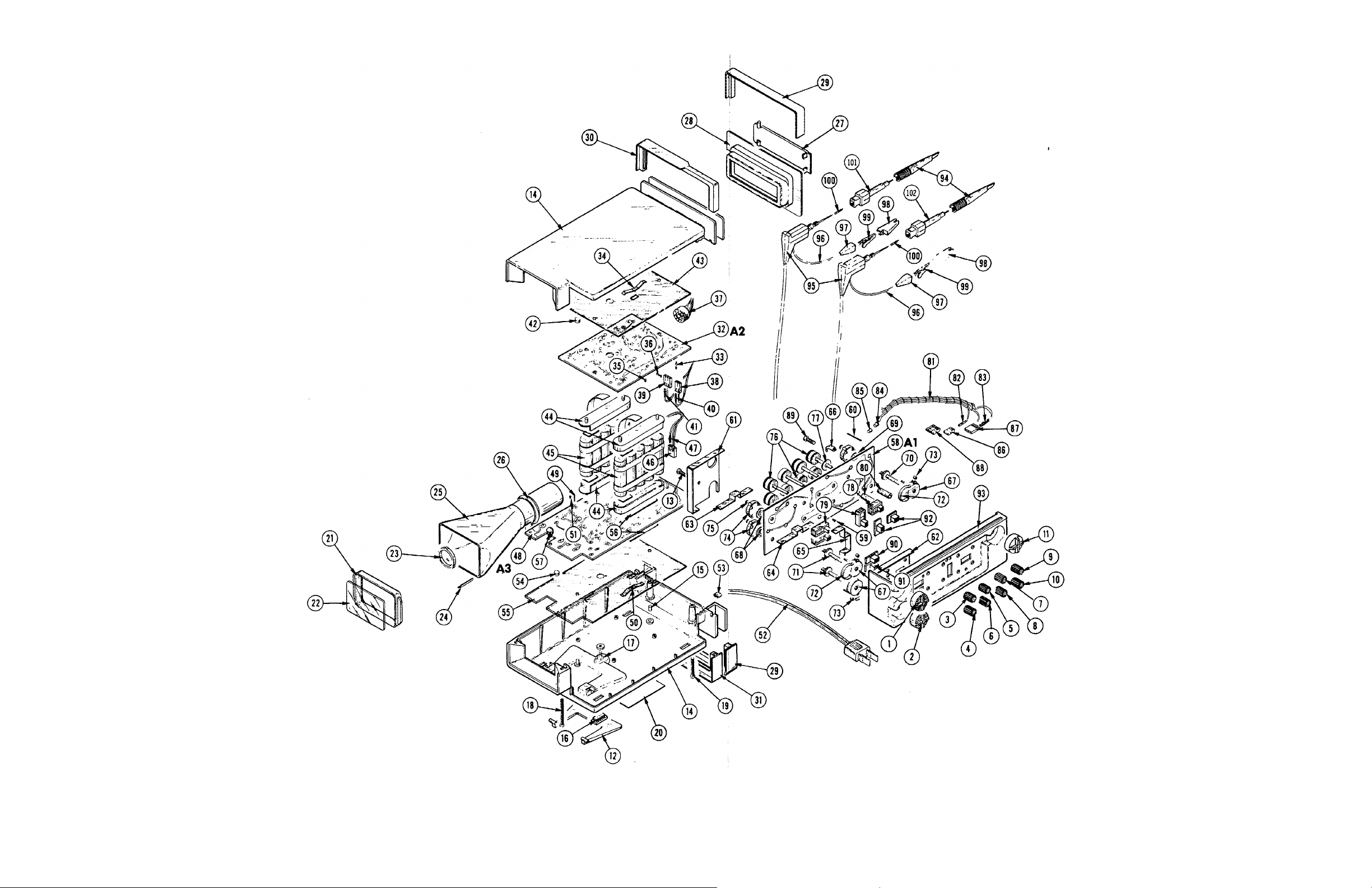
TM 9-6625-646-14&P
Figure 8-0. Mechanical Parts, Exploded View
8-17/(8-18 blank)
Page 70

TM 9-6625-646-14&P
Figure 8-1. Block Diagram.
8-19/(8-20 blank)
Page 71

TM 9-6625-646-14&P
Figure 8-1A. A1 Input Circuit Board (Front).
Figure 8-1B. A1 Input Circuit Board (Rear).
8-21/(8-22 blank)
Page 72

TM 9-6625-646-14&P
Figure 8-1C. Waveform Conditions.
Page 73

TM 9-6625-646-14&P
Figure 8-1D. Vertical Amplifier
8-23/(8-24 blank)
Page 74

TM 9-6625-646-14&P
Figure 8-1E. Vertical Amplifier.
Page 75

TM 9-6625-646-14&P
Figure 8-2. A2 Amplifier Circuit Board.
8-25/(8-26 blank)
Page 76

TM 9-6625-646-14&P
Figure 8-2A. Waveform Conditions.
Page 77

TM 9-6625-646-14&P
Figure 8-2B. Horizontal and Vertical Output Sweep and Trigger.
8-27/(8-28 blank)
Page 78

TM 9-6625-646-14&P
Figure 8-3A. A3 Power Supply Circuit Board, SN B040000-up.
8-29/(8-30 blank)
Page 79

TM 9-6625-646-14&P
Figure 8-3B. A3 Power Supply Circuit Board, below SN B040000.
8-31/(8-32 blank)
Page 80

TM 9-6625-646-14&P
Figure 8-4. CRT Circuit.
8-33/(8-34 blank)
Page 81

TM 9-6625-646-14&P
Figure 8-5. Power Supply.
8-35/(8-36 blank)
Page 82

Page 83

PIN: 055775-000
 Loading...