

Page 1

177 STANDARD
TEST FIXTURE
SERVICE
Page 2
WARNING
COMMITTED
m EXCELLENCE
THE
ARE FOR USE BY QUALI
TO
PERFORM ANY SERVI
CONTAINED
UNLESS YOU
FOLLOWING SERVICING INSTRUCTIONS
AVOID PERSONAL INJURY, DO
CI
IN OPERATING INSTRUCTIONS
ARE QUALI
PLEASE CHECK FOR CHANGE INFORMATION
AT
FI
ED
PERSONNEL ONLY.
NOT
NG OTHER
FI
ED
THAN
TO DO
THAT
SO.
THE REAR OF THIS MANUAL.
Tektronix,
P.O.
Beaverton,
070-1472-00
Product Group 48
Box
Inc.
500
Oregon
97077
177 STANDARD
TEST FIXTURE
SERVICE
INSTRUCTION
Serial
Number
MANUAL
_____
First Printing JUL 1973
Revised JUN 1983
_
Page 3
Copyright ®
Contents of this
form without the written permission of Tektronix,
1973
Tektronix,
publication may not
Inc.
All
rights reserved.
be
reproduced
Inc.
in
any
Products of Tektronix,
by U.S.
TEKTRONIX,
registered trademarks of Tektronix,
is
Printed
are reserved.
Each
or stamped
deSignates the country of manufacture.
of the
unique to
United States have six unique digits. The country of
manufacture
and
foreign patents and/or pending patents.
TEK,
a registered trademark of Tektronix
in
U.S.A. Specification
INSTRUMENT SERIAL NUMBERS
instrument has a serial number
on
serial number are assigned sequentially and are
each
is
identified
Inc.
and
its subsidiaries are covered
SCOPE-MOBILE,
and
the chassis. The first number or letter
instrument. Those manufactured
as
follows:
and
Inc.
U.K.
price change privileges
on
~
TELEQUIPMENT
Limited.
a
pa~el
insert, tag,
The
last five digits
in
are
the
BOOOOOO
100000
200000
300000
700000
Tektronix, Inc., Beaverton, Oregon, USA
Tektronix Guernsey, Ltd.,
Tektronix United Kingdom, Ltd., London
Sony/Tektronix, Japan
Tektronix
The
Holland,
Netherlands
NV,
Channel Islands
Heerenveen,
Page 4
177 Service
SECTION 1
SECTION 2
SECTION 3
SECTION 4
SECTION 5
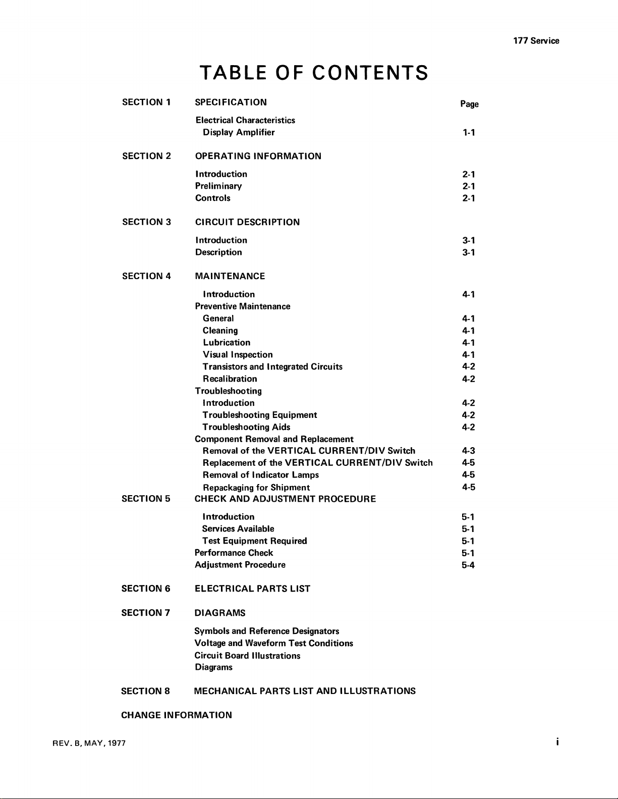
TABLE
SPECI
FICATION
Electrical Characteristics
Display
OPERATING
Introduction
Preliminary
Controls
CIRCUIT DESCRIPTION
Introduction
Description
MAINTENANCE
Introduction
Preventive Maintenance
General
Cleaning
Lubrication
Visual Inspection
Transistors
Recalibration 4-2
Troubleshooting
Introduction
Troubleshooting Equipment 4-2
Troubleshooting Aids 4-2
Component Removal and Replacement
Removal
Replacement
Removal
Repackaging
CHECK
Amplifier
of
of
AND
OF
INFORMATION
and
Integrated Circuits 4-2
the
VERTICAL
of
the
I ndicator Lamps
for
Shipment
ADJUSTMENT PROCEDURE
CONTENTS
CURRENT!DIV
VERTICAL
CURRENT!DIV
Switch 4-3
Switch 4-5
Page
1-1
2-1
2-1
2-1
3-1
3-1
4-1
4-1
4-1
4-1
4-1
4-2
4-5
4-5
REV.
B.
MAY. 1977
SECTION 6
SECTION 7
SECTION 8
CHANGE
INFORMATION
Introduction
Services Available
Test Equipment Required
Performance Check
Adjustment Procedure
ELECTRICAL
DIAGRAMS
Symbols and Reference Designators
Voltage and Waveform Test Conditions
Circuit Board
Diagrams
MECHANICAL
PARTS LIST
Illustrations
PARTS LIST
AND
ILLUSTRATIONS
5-1
5-1
5-1
5-1
5-4
Page 5

177
Standard
Tes
t
Fixture.
177 Service
®
Page 6
SPECIFICATION
The
177
is
a plug-in test fixture designed
the
577
-D
1 or
D2
Curve Tracer
measure the characteristics of a variety of two, three, and
four term ina
The
I devices.
177 features:
to
operate with
to
form a system
to
Section
The 100 V,
normally interlocked and are energized by closing
protective box cover
button.
Only those voltages
for Emitter-Base Leakage
400
V, and 1600 V collector ranges are
or
by pushing the interlock
that
are
not
interlocked are available
or
Breakdown tests.
1-177
Service
the
defeat
Two switch-selected sets
parison tests.
to
Kelvin sensing
current
the various
2 A/DIV.
step generator
emitter
compensation control.
levels.
A term inal selector switch
test
Vertical deflection factors ranging from
External front-panel jacks permitting access
(E) terminals.
A variable
provide accurate measurements at high
configurations.
output
-12,
0,
of
test jacks, perm itting com-
that
perm its easy selection of
and device-under-test base
+12 volt
DC
output
0.2 nA/DIV
to
the 577
(B)
and
and a looping
to
The
electrical and environmental characteristics shown
are valid for instruments operated
ture
range from +1O°C (+50°F)
five-minute warmup,
+30°C (+86°F).
E
lECTR
Display
Amplifier
Accuracy (percent of highest on-screen value)
Vertical Collector Current: Total system accuracy of
the
577-177-D1
magnified.
Deflection Factor, Vertical
Collector Current: 2
sequence, unmagnified, and
DIV, magnified.
if
calibrated
ICAl
CHARACTER ISTICS
or
D2
nA/DIV
in
an ambient tempera-
to
+40°C (104°F) after a
at
+20°C (+68°F)
is
3%, unmagnified, and 4%,
to
2 AlDIV
0.2 nA/DIV
in
to
a 1-2-5
200
mAl
to
®
1-1
Page 7

Page 8
Section
2-177
Service
OPERATING
Introduction
The
177 Test Fixture operates with a Tektronix 577
the
D1
or
D2
Curve Tracer and
of
1 or
of
the
front·panel controls of
D2
This section
description
577 -177
operating procedure.
-D
the
Operators Manual for a complete
Display
manual gives a brief functional
Preliminary
For initial preparation, refer
tions
section of
The
Operators Manual contains operating instructions,
well
as
general and specific application information.
the
577-177-D1 or D2 Operators Manual.
Unit
the
to
the
Operating Instruc-
as a system.
177. See
INFORMATION
BASE GROUNDED MODE (Base terminal
polarity
Disconnects
generator
minal
INPUT Connector.
Applies step generator
terminal.
to
the
to
that
output
the
base term
the
are
the
as
step generator
is
switched as follows):
EM
ITTER TERM
OPEN (OR EXT)
STEP GEN
EMITTER-BASE BREAKDOWN
Grounds
sweep voltage
voltage
ranges
is
is
inverted, and
the
emitter
and connects
front-panel EXT BASE OR
inal
emitter terminal. Only
not
interlocked are available.
the
em itter term inal
term inal from
the
output
and applies
to
emitter ter-
the
the
the
grounded,
the
step
EM
IT
em itter
collector
collector·
Controls
This
is
a brief description of
front-panel controls. More detailed information is given
the
Operators Manual.
EMITTER GROUNDED MODE
grounded; Base terminal
BASE TERM
STEP GEN
Applies step generator
tions
of
OPEN (OR EXT)
Disconnects
generator
the
front-panel EXT
Connector.
SHORT
Disconnects
generator
the
output
output
is
switched as follows):
test
fixture.
the
base terminal from
and connects base terminal
the
base terminal from
and grounds
the
functions of
(Emitter terminal
output
BASE
to
the
OR
the
base term inal.
base connec·
the
EM
IT
INPUT
the
the
in
is
step
to
step
STEP GEN OUTPUT Connector
Provides
EXT
Provides
depending
GROUND
Provides for external ground connection.
LEFT-RIGHT Switch
Three position
either
center position disconnects all terminals
term ina
together and are connected
generator, or
position of
Test Adapter
Two sets
for testing various sem icond uctor devices.
external access
BASE
OR
external access
on
the
left
Is.
The
the
of
to
the
step generator
EM
IT
IN
Connector
to
the
base or em itter
the
position of
toggle switch for applying
or
right set of terminal connectors.
em itter term inals are always connected
to
the
Terminal Selector switch.
Terminal Jacks
five recessed jacks accepting various adapters
the
Terminal Selector switch.
to
either ground,
collector sweep depending
test
except
output.
term
signals
the
emitter
to
the
on
ina
The
step
the
Is,
to
®
2-1
Page 9

Page 10
Section
3-171
Service
CIRCUIT
DESCRIPTION
Introduction
This section of the manual contains a description of the
circuitry
schematic diagrams, with
values, are shown on
manual.
in
the 177 Standard Test Fixture. Complete
component
the
pullout pages at
numbers and parts
the
rear
of
this
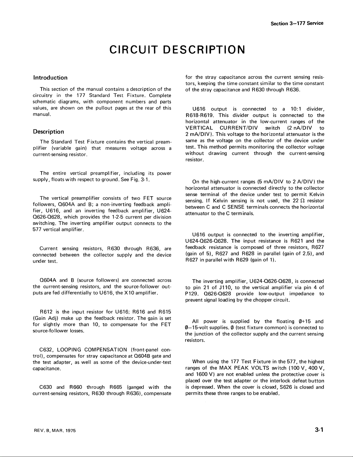
Description
The
Standard
plifier (variable gain)
current-sensing resistor.
The
entire vertical preamplifier, including its power
supply, floats with respect
The
vertical preamplifier consists
followers,
fier, U616, and an inverting feedback amplifier, U6240626-0628,
switching.
577 vertical amplifier.
Current
connected between
under test.
Test
Fixture contains
that
to
0604A
The
and
B;
a non-inverting feedback ampli-
which provides
inverting amplifier
sensing resistors, R
the
collector supply and
the
vertical pream-
measures voltage across a
ground. See Fig. 3-1.
of
two FET source
the
1-2-5 current per division
output
630
connects
through R636, are
the
to
device
the
for
the
stray capacitance across
tors, keeping
of
the
U616
R618-R619. This divider
horizontal
VERTICAL CURRENT/DIV switch
2 mA/DIV). This voltage
same
test. This method permits monitoring
without
resistor.
On the high-current ranges
horizontal
sense terminal of
sensing. If Kelvin sensing
between
attenuator
U616
U624-0626-0628.
feedback resistance
(gain of
R627
the
time
constant
stray capacitance and R630 through R636.
output
attenuator
as
the
drawing
attenuator
C and C SENSE terminals connects
to
output
5L
in
parallel with R629 (gain
is
connected
in
to
voltage on
the C term
R627 and R628
the
current
is
connected directly
the
device under
ina
is
connected
The
input
is
composed of three resistors, R627
the
current sensing resis-
sim ilar
to
output
the
the
collector of
through
is
Is.
is
low-current ranges
horizontal
(5
mA/DIV
test
not
used,
to
the
resistance
in
parallel (gain of
of
1).
to
the
time
constant
a 10: 1 divider,
connected
(2
attenuator
the
the
collector voltage
the
current-sensing
to
to
to
the
inverting amplifier,
is
R621 and
to
of
nA/DIV
is
device under
2 A/DIV)
the
collector
permit Kelvin
22.Q
resistor
the
horizontal
2.5L
and
the
the
to
the
the
the
0604A
the
puts are fed
R612
(Gain Adj) make up
for
source-follower
C632, LOOPING COMPENSATION (front-panel
troll.
the
capacitance.
C630 and R660 through R665 (ganged with
current-sensing resistors, R630 through R636), compensate
REV.
and B (source followers) are connected across
current-sensing resistors, and
differentially
is
the
input
slightly more than 10,
losses.
compensates for stray capacitance
test
adapter, as well as some
B,
MAR.
1975
to U 616,
resistor for U616; R616 and R615
the
feedback resistor.
the
source-follower out-
the
X 1 0 ampl ifier.
to
compensate for
at
of
the
0604B
device-under-test
The
gain
the
gate and
is
FET
con-
the
set
The inverting
to
pin
21
P129.
prevent signal load
0-15-volt
the
resistors.
ranges of
and 1600
placed over
is
permits these three ranges
0626-0628
All
power
junction
When using
depressed. When
amplifier,
of
J110,
to
provide low-output impedance
ing
by
is
supplied by
supplies. 0 (test fixture common)
of
the
collector supply and
the
177
the
MAX
PEAK VOLTS switch
V)
are
not
enabled unless
the
test
adapter
the
U624-0626-0628,
the
vertical amplifier via pin 4
the
Test
cover
to
chopper
Fixture
or
be
the
the
interlock
is
closed,
enabled.
circu it.
floating 0+15 and
is
the
current
in
the
577,
(100V,
the
protective cover
S626
is
connected
connected
sensing
the
highest
400
defeat
button
is
closed and
of
to
to
V,
is
3-1
Page 11

::II
m
<
.tIl
s::
»
::0
VERTICAL
CURRENTI
DIV
DEVICE C
(")
~'
;:+'
COLLECTOR SUPPL Y
FROM 577
____________
Jll0
C630
,
,
,
I
r---
I
I
I
,
,
,
,
I
I
I
I
L_
R636
THROUGH
R613
R630
J¥+15
R612
.6'-15
R615
and
GAIN
.Il'+15
.6'-15
R616
R618
i":-C------------------------------~H~I~G;H~C~U~R~R;E~N~T--------------~04~>-------
r--
.l...
T B I
L__
DEVICE UNDER TEST I
(5mAto2A)
1___
24
-----
R619
R621
CURRENT
LOW
A
""iiii---------------------------'
J¥+15
.6'-15
R629
-.,
X5
I
R6Z8
______
R627
.6'+15
,
X2.5
r-
..J
I
Xl
~--~~----~--------------:2~1~1~~t.~VE:ri~:~T~~~~AL
U624,0626
0628
,d-15
L---------------:.6'~=~V~E:R:T~~IC~A~L~S~I~G~N~A~L~C-O~M-M--O-N----~2~2~.~~~~
(2
nA
- 2 rnA)
______________________________________________
I
I
I
~,>---,,--..,
I
i SUPPLY
~
I
;>--Jr--f-_-.J
I
I
I
I
I
I
I
I
I
I
I
I
I
I
I
I
I
I
I
I
,
I
I
I
I
I
I
I
I
I
I
I
I
I
~A~1'~
I~
Jll0
I
F~~~~~G
AMPLIFIER
• .6'
TO
HORIZONTAL
ATTENUATOR
o
~
...
ii'
...
0'
;:,
I
...
"-I
"-I
~
<
~'
Page 12

5628,
the
177
interlock_
the
safety-interlock
front
panel) may be pressed
defeat
switch (red
to
defeat
button
the
safety
on
Circuit
WARNING
Oescription-177
I
Service
The
using
option
100
V and
the
protective cover
in
the
177 (see Fig. 3-2
400
V supplies may be enabled
or
the
defeat
for
details).
switch
by
without
a wiring
To
the
between
To
the
between
enable
Interlock
point
enable
Interlock
point B and
This modification
supply can
likely lethal.
ING note should
the
the
+l00·volt
Defeat
A and
+400-volt
Defeat
switch,
point
switch.
point
supply
supply
is
not
be
lethal and the
If
this modification
be
permanently attached to the
without
remove link A
X.
without
remove link B and
X.
using
using
recommended. The 100 V
400
V supply
is
made a WARN-
is
very
177.
the
protective
and
connect a wire
the
protective
connect
box
or
box
of
a wire
®
Fig.
3-2.
100 V and
400 V Interlock
Defeat
bypass
option.
3-3
Page 13

Page 14

MAINTENANCE
Section
4-177
Service
I ntrod uction
This section of
in
preventive and corrective maintenance, with
troubleshooting.
PREVENTIVE
the
manual contains information for use
MAINTENANCE
General
Preventive
spection, lubrication,
ed
on
a regular basis improves
severity
determ ines
of
the
the
maintenance
etc.
environment
frequency
consists
Preventive
instrument
in
wh ich
of
maintenance.
of
cleaning, visual
maintenance
the
instrument
Cleaning
The
177
Test
Fixture
operating cond itions require. Accumulation
instrument
breakdown,
Exterior. Loose
instrument can
paint brush.
dislodging loose
controls. Dirt
dampened
cleaners should
Interior. Dust
removed occasionally
high-humidity environments.
using
a mild
applicator
can cause leakage currents and
especially
dust
be
removed
The
paint
dust
that
remains can
in
a mild
be
avoided.
in
the
dry,
low·velocity air. Remove any remaining
detergent
is
and
useful for cleaning circuit boards.
should
in a hum
accumulated
with a soft
brush
on and around
be
detergent
to
and
interior
prevent
Blowout
water
be
cleaned as
id
atmosphere.
on
the
cloth or a small
is
particularly useful for
removed with a
water
solution. Abrasive
of
the
instrument
electrical
accumulated
solution. A
some
perform-
reliability.
often
of
dirt
component
outside
the
front-panel
soft
should
conduction
dirt
cotton-tipped
aids
The
is
used
in
of
cloth
dust
with
to
in-
as
the
the
be
in
Lubrication
The reliability of
other
moving parts can be maintained if
properly lubricated.
switch contacts. Lubricate switch
grease (such
as
potentiometers,
Use
Tektronix
a cleaning·type
detents
Part No.
006-0219·00).
rotary switches, and
they
lubricant
on
with heavier
NOTE
bushings and potentiometers that
Shaft
are
not
should be lubricated with a lubricant (such
Tektronix Part No. 006-2574-00) that will
the electrical characteristics.
lubrication
kit
(Tektronix Part
Do
not
No.
not
over-lubricate. A
003-0342-01)
available.
Visual Inspection
The
177
Test
Fixture
for such
tions, improperly seated transistors, damaged circuit
and
obvious. However, particular care
damaged
cates
important
prevent recurrence
defects
heat
damaged parts.
The
corrective
components
other
trouble
that
as
the
should
broken
procedure
are
found.
in
the
cause
of
the
damage.
be
inspected occasionally
connections,
for
Overheating usually indi-
instrument.
of
overheating
loose pin connec-
most
visible
must
be
It
be
defects
taken
is,
therefore,
corrected
NOTE
Connecting the device under test to the test fixture in
a manner that causes current flow
sensing resistors
Fig.
4-1
and the Kelvin Sensing Check in the Trouble-
can
burn
out
in
the Kelvin
these resistors. See
shooting section.
are
rotary
sealed
as
affect
is
boards
if
heat
kept
is
to
Avoid the use
damage the plastics used
of
chemical cleaning agents that might
in
the instrument.
Do
use chemicals that contain benzene, toluene, xylene,
acetone, or similar solvents.
REV B
JUL
1979
not
The
current sensing resistors (R630 through R636)
can be damaged
disabling circuit
if
the vertical current over-range
in
the
577
is
not
functioning
properly. Check the over-range circuit after
ment
of
a current-sense resistor.
replace-
4-1
Page 15

Maintenance-177
Service
Troubleshooting Equipment
The
the
following
177:
equipment
is
useful for troubleshooting
Fig. 4-1 .
Location
of
Kelvin
sense
resistors.
Transistors and Integrated Circuits
Periodic checks of individual transistors and integrated
circuits are
operation
Sub·standard performance
performance check
in
not
the
recommended.
equipment
or
calibration procedure.
The
as reflected
is
normally detected during a
best check
by
performance.
Recalibration
To
ensure accurate measurements, check
calibration after each
operation,
or
if
the
year . Replacement
bration of
the
instructions are given
Adjustment
procedure can
section.
also be helpful
1000 hours (approximately) of
instrument
of
components
affected circuits. Complete calibration
in
The
Performance Check/Adjustment
is
used infrequently, every
may necessitate recali-
the
in
locating troubles.
the
instrument
Performance Check/
is
their
1. Semiconductor Tester.
transistors, diodes, and FETs used
helpful. A curve tracer, such as
577 gives
checking circuit
2.
the
most complete information.
DC
Voltmeter and
voltages and an
resistances and diodes are required.
20,000
for circuit
ohms/volt
load
ing
VOM
when
Some
means of testing
in
the
Tektronix
Ohmmeter.
ohmmeter
For
can be used
if
measuring voltage
the
A voltmeter for
most applications a
allowances are made
at
ance points.
3. Test
10
MHz
vertical deflection factor
be used
Oscilloscope. An oscilloscope with a
frequency response and 10 mV/Div
is
suggested. A 10X probe shou
to
reduce circuit loading.
Troubleshooting Aids
Diagrams. Circuit diagrams are given on
the
Diagrams section .
trical value
of
the
to
identify
of
each
Diagrams section for definition of
components
Switch Wafer
the
shown on
each wafer
the
code
of
end
front
or
diagram s are coded
in
the
is
the
wafer number counting from
the
switch.
rear
of
The
component
component
are shown. See
.
Identification. Rotary switch wafers
to
switch assembly.
The
letters F and R indicate
the
wafer performs
The
For example, a wafer designated 2R indicates
the
second wafer.
Circuit Description.
describes each circuit.
tion of
diagram
the
theory of circuit operation illustrated by a block
of
each section of circuitry. Following
Diagram description
that
contains unique or complex circuitry.
The
Circuit Description, Section 3,
The
section contains a brief descrip-
is
a detailed description of each circuit
foldout
number
the
ind icate the position
number portion
the
switching function.
the
instrument
575,
576
, or
for checking
high imped-
DC
to
10 V/
Div
pages in
and elec-
the
first page
symbols used
the
mounting
whether
the
the
the
rear of
Block
is
to
Id
of
of
TROUBLESHOOTING
Introduction
The
following information
troubleshooting
sections
information
of
this manual should
to
the
177. I nformation contained
aid
in
locating circuit defects (see
is
provided
be
used with
Operating and Circuit Description sections).
4-2
to
the
facilitate
in
other
following
the
Transistor and
The
lead configurations
177 Test Fixture are shown with
on
the
schematic diagram
Voltages and Waveforms.
forms are shown
Integrated Circuit Lead Configuration.
of
the
transistors and ICs in
the
in
blue
foldout
I
mportant
on
the
circuit board
aprons.
voltages and wave-
diagrams. Portions
photos
of
the
the
circuits mounted on circuit boards are enclosed by blue
lines
or
boxes.
®
Page 16

Maintenance-177 Service
Capacitor Identification. Capacitor values of disc
capacitors are marked on the capacitor body and electrolytic
capacitor values are either marked on the capacitor body or
are
color coded
Diode
enclosed diode
a dot. For diodes using a series of
Fig.4-2.
(see
Fig_
4-2).
Color Code. The cathode end of each
is
indicated by a stripe, a series
of
stripes, the color code
""'--VELLOW
5
47 x 10
6
=
4.7
capacitor
pF
",F
color
code.
Example
INDICATES
OR
4.7 x 10-
of
Electrolytic
glass-
stripes, or
1472-5
identifies either
the
Tektronix part number or the JEDEC
number. This code follows the standard color code except
that
a pink first band indicates a Tektronix part number,
i.e.,
pink-brown-gray-green
indicates Tektronix Part
Number 152-0185-00.
Circuit Boards. A photograph of each circuit board, with
circuit components identified,
the
schematic diagram relating most directly
board. Some board photos may be placed on
the
preceding circuit diagram. Each circuit board photo
sectioned by a grid system
is
included on
to
facilitate rapid location of
the
apron of
to
the circuit
the
back of
components by component number.
COMPONENT REMOVAL
of
the
Removal
VERTICAL
AND
REPLACEMENT
CURRENT/DIV
Switch
1. Remove the right-end (viewed from the front) panel
of
the
177.
Remove
the
left-end panel). Note
facilitate re-assembly. Machine screws hold
cover and self-thread
Fig. 4-3 for location of screws.
the
bottom-cover screws (including one from
the
two types
of
screws used,
the
ing
screws hold the end panels. See
to
bottom
is
SELF
THREADING
Fig. 4-3. Location
of
cover screws.
MACHINE
SCREWS
SELF
THREADING
1472-6
REV. B,
MAR.
1975
4-3
Page 17

Maintenance-177
2.
Turn the CURRENT/DIV switch
the
two
hex socket-head set screws
4-4). Loosen the set screw and turn
Fig.
DIV
knob
to
Note
the
screw and remove the knob and
through
the
make
position
front
Service
the
panel.
other
set screw accessible.
of
the
knob skirt. Loosen the set
WARNING
to
expose one of
(A
in
the
diagram,
the
CURRENT/
insulating bushing assembly
WARNING
Do
not
replace the insulating bushing with
un-insulated bushing,
as
high
as
1900 volts. Since
including entire switch assemblies,
place components and parts with the correct parts.
as
the switch shaft is elevated to
many
I
of
the components,
are
elevated,
an
re-
Replace
shown
isolates
which the
in
this coupling with only the part number
the Mechanical Parts List. This coupling
the
knob set screw from
voltage may be as high as 1600 volts.
the
switch,
o
o
hex socket-head screws.
Pull knob and bushing assembly
away from switch.
nut
Remove hex
from view
in
and one hidden
this drawing.
o
4-4
Pull the
Unsolder
wafers.
"';.'"
all
to
.he
leads
re.J
at
the
switch
__
....6
Fig.4-4.
Removal
of
VERTICAL
CURRENT/DIV
Switch.
®
Page 18

Maintenance-177 Service
Using a 12-point box-end wrench,
loosen the
switch
remov ing the hex nuts).
Refer
removed)
two
hex nuts
to
the
circuit
to
Fig.4-5
to
faciliate switch replacement.
(8
board (hold the screw head, C,
(drawing
in the diagram)
of
or
open-end wrench,
the
leads
that
that
hold
while
must
the
be
Removal
Knob
shown in Fig. 4-3.
These
sleeve.
with
the
Unsolder the
Red
mounted
pushing the assembly
from
Repackaging
If the Tektronix instrument is
Tektronix Service Center for service or repair, attach a tag
showing: owner (with address) and the name
individual
complete
service required.
of
Indicator Lamps
Sirt
Lamps. Remove the
lamp assemblies (gray plastic)
To
remove the lamp assembly,
needle-nose pliers
sleeve.
leads
Dangerous Voltage Lamp. This lamp assembly
in
a rubber grommet
the rear
while
for
at
your firm
instrument serial nuinber and a description
and
and
remove the lamp assembly.
out
pull ing
Shipment
that
right
end
from
snap
into
grasp
pull
the assembly away
and
may be removed
through the
from
the
can be contacted. Include
front
front).
to
be shipped to a
the 177
the plastic
the assembly
from
by
panel (push
of
an
of
the
as
is
Fig. 4-5.
replace
circu
Replacement
location
the
Unsolder the leads
it
board.
of
VERTICAL
of
the
leads
that
CURRENT/OIV
must
and
pull the switch away
VERTICAL
Switch
Place the switch mounting screws
holes
and
mounting
the more
the
a
flat
to
screwd river, tu rn the screw clockw
start the
loosen the
allow the
screw-head.
nuts on the opposite side
accessible switch-assembly screw. Partially tighten
next
nut.
Attach a piece
object (stick, screwdriver blade, etc.).
the tape
nut
nut
screw
Tighten the
Complete tightening
place the lock washer
of
tape having adhesive on
and
place the
on the screw.
on the opposite
to
turn.
nut
If
with
a wrench while holding the
both
of
the board
nut
the screw cannot be turned,
side
nuts, making
be
removed
switch.
to
remove
from
and
the
CURRENT/DIV
into
the
circuit
board
and
hex
nut
on
both
sides,
to
Attach
over the screw. With a
ise
just
of
the board enough
sure
are
tight.
the
far enough
that
both
nut
to
to
Save and re-use the package
was shipped.
available, repackage the instrument as follows:
Surround the instrument with
protect the finish
corrugated cardboard
having inside dimensions
than the instrument dimensions. Cushion the instrument
tightly packing three inches
by
foam between carton and instrument, on
carton with shipping tape
The carton test strength
pounds.
If the original packaging
of
the instrument. Obtain a carton
of
in
which your instrument
is
unfit for use
polyethylene sheeting
the correct carton strength and
of
no
less than six inches more
of
dunnage
or
industrial stapler.
for
your instrument is 200
or
urethane
all sides. Seal
or
not
to
of
Resolder all
REV JAN 1983
leads
into
their
respective switch terminals.
4-5
Page 19

Page 20

Section
5-177
Service
CHECK
Introduction
This
section
adjustment
check
specifications.
circuitry
Adjustment
made,
components
For
the
instrument
proced ures.
the
instrument
to
within
or
after
may
initial inspection, using
of
the
manual
The
Check
operation
The
Adjustment
the
design capabilities.
is
generally required
a long
time
interval
affect
instrument
side covers
in
AND
contains
procedure
against
procedure
in
accuracy.
the
check
place.
ADJUSTMENT
separate check and
is
provided
the
instrument
returns
after
a repair
which normal aging
proced~re,
has
to
the
been
of
leave
Set
the
Resistance
Q
1
10 Q
100
Q
1kQ
10
kQ
100
kQ
1MQ
10 MQ
controls
PROCEDURE
Watts Accuracy
10
5
1/2
1/4
1/4
1/8
1/8
1/8
PERFORMANCE CHECK
as follows:
1/4%
Services Available
Tektronix,
calibration service
offices.
representative
Inc., provides
Contact
for
complete
at
local field service
your
local
further
information.
Tektronix
Test Equipment Required
The
following
calibration
for
equipment
operating
bridge.
impedance,
1000;
These resistors are available from
(Tektronix
resistors are included
177
Part
1.
Digital
2.
Capacitor.
tolerance,
3.
Shunt
4.
Extender
without
Number
within
Accuracy,
test
equipment,
of
the
177
Standard
is
assumed
the
Voltmeter
500
MQ.
Capacitance,
±20%.
resistors. Range 1 Q
Part Number
Cable, (to
removing
067-0721-00.
to
be
listed specifications.
(4·1/2
0.01%; voltage range,
See
footnote
067-0691-00).
in
this kit.
permit
the
577
0.01
instrument
or
equivalent,
Test
correctly
digits)
to
making
bottom
or a DC
1, Table 5-1.
pF;
working
10 MQ.
Tektronix,
Two
adjustment
panel)
repair and
centers
and field
Field Office
is
required
Fixture.
calibrated and
±5
volts;
See
the
Inc.,
200
Tektronix
All
voltage
voltage,
table.
as a kit
Q,
to
or
test
input
1%
the
577-01
MAX PEAK VOLTS
SERIES
COLLECTOR SUPPLY
V AR IABLE COL-
HORIZ
NUMBER
All Dark
Horizontal POSITION
Vertical POSITION
RESISTORS
POLARITY
LECTOR
STEP FAMILY
X10
VOL
OF
Gray
VERT
%
TS/DIV
STEPS
Buttons
MAG
or
02
6.5
.12
+DC
o
200
V,
cou nterclockw i se
and Knobs in,
SINGLE
out
Centered
Centered
COLLECTOR
except:
177
VERTICAL
RENT/DIV
Terminal
LEFT-RIGHT
CU
R-
Selector
.2A
EMITTER
BASE
TERM,
Off
1. Check Vertical Preamplifier Balance
a. Vertically and
graticule
center.
horizontally
position
GROUNDED,
STEP
GEN
the
spot
to
REV.
B, SEPT.
1974
5-1
Page 21

Performance Check-177 Service
b. Switch the
throughout its
c.
CHECK-There
division of vertical movement while switching the VERTICAL
CURRENT/DIV through its range. (It may first
to
adjust R610 as in Step 1
range.
VERTICAL
should be not more than 0.5 major
CURRENT/DIV switch
be
necessary
of
177 adjustment procedure.)
2. Check Vertical Preamplifier Common-Mode
Rejection
a.
Set the controls
VERTICAL
RENT/DIV
COLLECTOR SUPPLY
POLARITY
Vertical POSITION
Horizontal POSITION
LEFT-RIGHT
b. Connect a patch cord between the
terminal
the plug in the bottom
1/4-inch ring terminal at one
as
connection
the
(front
E-Z
HOOK TIP
to
TP630.
CUR·
panel)
as
follows:
10nA
AC
centered
centered
Off
and
TP630. To
panel
of
end
of
C630. A hook
1,
provides a convenient
117
GROUND
reach
TP630, remove
the 117. TP630
tip,
means
is
such
of
3.
Check Vertical Current Per Division
a.
Push
Xl0
VERT MAG in. Reset the VERTICAL
CURRENT/DIV
VARIABLE COLLECTOR %
COLLECTOR SUPPLY CIRCUIT BREAKER
b.
Remove the C to E patch cord.
c.
Reset the controls as follows:
STEP/OFFSET AMPL
OFFSET MULT
STEP
SINGLE
OFFSET
ZERO
AID
VERTICAL CURRENT/DIV
LEFT-RIGHT
d.
a
Connect the DVM between E
set
of
terminals. Connect a
in Table 5-1,
terminals, right
to 2A, switch LEFT-RIGHT
FAMILY
10
second
column) between the
side.
to
100,
.1V/Step
0.000
press
out
in
2 nA
Off
and
Mil,
1/4%, resistor
to
RIGHT, turn
and
wait for the
to
open.
B on the right-side
(as
shown
117
Band
C
c.
Connect a patch cord between the
terminals, right
d.
Switch the LEFT-RIGHT switch
e.
Reset
f.
CHECK-Vertical deflection should
major divisions.
g.
Return the
the LEFT-RIGHT switch
h. Disconnect the ground
patch cord between C
side.
the
VARIABLE
VARIABLE
COLLECTOR %
COLLECTOR %
to
Off.
lead
and
E term inals.
WARNING
117 C and
to
RIGHT.
to
be
less
from TP630.
I
100.
than four
to
O.
Switch
Leave
the
E
e.
Switch the LEFT-RIGHT switch
DVM reading.
f.
Vertically position the spot
NOTE
The DISPLA Y
be
in the
FIL
TER NORM button
out
position to reduce the display noise
high sensitivities.
g.
With the OFFSET
bottom graticule line.
CHECK-The
h.
the DVM reading
shown in Table 5-1, columns 3
i. Switch the
STEP/OFFSET AMPL
MUL
difference
is
step
e,
VERTICAL
to
the next settings
to
RIGHT. Note the
to
the eighth graticule line.
may
T,
position the spot
in
DVM reading, relative
should
and
be
within
4.
CURRENT/DIV
in
the table.
have to
at
to
the
the limits
and
to
Replace the plug in the
bottom
panel
avoid contact with potentially lethal voltage.
5-2
of
the 177 to
j.
Press
reading.
the OFFSET ZERO button in
and
note the DVM
REV JAN 1983
Page 22

Performance
Check-177
Service
k.
Position the spot to the eighth graticule line.
I.
Release
OFFSET
the OFFSET ZERO button. With the
MUTL,
position the spot
to
line.
m.
be
within
CHECK-The
the limits shown in Table 5-1.
difference in the DVM reading should
n. Repeat the above procedure
VERTICAL
CURRENT/DIV
steps,
resistance specified in the table.
VERTICAL
CURRENT/
DIV
2 nA
5 nA
10
nA
20 nA
TABLE
STEP/ Resistor
OFFSET
AMPL
.1
V
.2V
.5V
V
1
5-1
(1/4%)
CoB
10 MQ
the bottom graticule
for
each
of
the
using
the value
of
Difference
in
DVM
Within
Reading ±3%,
B-E
±1nA
0.3200 V 0.0296 V
0.8000 V 0.0400 V
0.8800 V 0.0375 V
1.760 V
0.0638 V
VERTICAL
CURRENT/
DIV
.1
).LA
.2).LA
.5).LA
1
).LA
2).LA
5).LA
10).LA 10).LA
20).LA
50).LA 50).LA
.1
mA
.2
mA
.5
mA
1
mA
2mA
5
mA
10
mA
20mA
50
mA
.1
A
.2A
the
Pull
steps.
Xl0
TABLE
5-2
STEP/ Resistor in
OFFSET
AMPL
.1
).LA
.2
).LA
(1/4%)
CoB CoB
1
MQI
.5).LA
l).LA 100
kQ
I
2).LA
5).LA
10
kQ
20).LA
1
.1
.2
mA
mA
kQ
.5mA
1
mA
100 Q
2
mA
5mA
10
10mA
Q
20mA
50mA
.1
A
lQ3
.2A
VERT
MAG
and
proceed
Difference
DVM
Within
Reading ±3%,
±1nA
0.800 V 0.024 V
1.600 V 0.048 V
4.000 V 0.120 V
0.800 V 0.024 V
1.600 V 0.048 V
4.000 V 0.120 V
0.800 V 0.024 V
1.600 V 0.048 V
4.000 V 0.120 V
0.800 V 0.024 V
1.600 V 0.048 V
4.000 V 0.120 V
0.800 V
0.024 V
1.600 V 0.048 V
4.000 V 0.120 V
0.800 V 0.024 V
1.600 V
4.000 V
0.800 V
1.600 V
as
0.048 V
0.120 V
0.024 V
0.048 V
in the previous
50
nA
o. Switch the
2V
LEFT-RIGHT
4.400 V 0.1430 V
switch
to
Off.
p. Reconnect the DVM between Band C (or C SENSE).
q.
Proceed
as
in
steps
3 e through 3 h,
using
5-2.
r. Switch the
s.
Disconnect the DVM
llf
a DVM having an
the
formula:
where
V2 is
tile
100
meter
the
the
table.
Mil.
Rm
is
resistor in
less
than
LEFT-RIGHT
input
impedance
meter
reading,
input
impedance,
Do
not
switch
and
resistor.
of
V 1
is
and
use
a DVM having an
500
the
Rs
to
Off.
Mil
or
less is used, use
reading in
is
the
current
input
Table
impedance
Table
5-2,
sensing
50
.1
.2
t.
mAl
A
A
Push
50mA
.1
A
.2A
to
reset the COLLECTOR SUPPLY
10 Q
BREAKER.
u.
If
DISPLAY
FILTER
in.
4. Check Kelvin Sensing
a.
Set the controls
MAX
PEAK VOLTS
SERIES RESISTORS
Xl0
HORIZ MAG
HORIZ
VOL
Vertical POSITION
Xl0
VERT
VERTICAL
RENT/DIV
LEFT-RIGHT
TS/DIV
MAG
CUR-
as
follows:
1
1
was
Q3
Q3
4.000 V
0.800 V
1.600 V
used,
push
25
1.9
pull
5
mV,
COLLECTOR
centered
in
lA
Off
CIRCUIT
NORM
±4%
0.160V
0.032 V
0.064 V
button
2Magnification
the
.5A,
1A,
REV JAN 1983
and
occurs
2A
only
in
ranges in
the
the
577.
177.
These
measurements
check
3Measure
of
lead
and
near
contact
the
body
of
resistance.
low
value
resistors
to
reduce
the
effects
5-3
Page 23

Performance Check/
Adjustment-177
Service
b.
Place
an
013-0111-00 Diode Adapter in the
terminals, right side.
Place
a short, clean, piece
of
14
gauge
solid copper wire (preferrably tinned) in the adapter.
c.
Switch the
d.
Increase the
display eight divisions
e.
Horizontally position the bottom
LEFT-RIGHT
VARIABLE
of
vertical deflection.
switch
to
RIGHT.
COLLECTOR % control to
of
the trace
graticule center line.
f.
CHECK-The
horizontally, in either direction, not more than
top
of
the display should be displaced
15'mV
(three major divisions) from the graticule center line.
Fig.
5-1
for
an
example
l R
of
a typical display.
177
to
See
b. Increase
VARIABLE
eight-division vertical display.
c.
Horizontally position the
graticule center.
d.
CHECK-The
from
graticule center
If
this requirement cannot
incorrect adjustment
top
of
not
more than ±7
of
Vertical GAIN
ADJUSTMENT PROCEDURE
Initial Control Settings
MAX
PEAK VOLTS
SERIES RESISTORS
VARIABLE
LECTOR
HORIZ
Horizontal POSITION
HORIZ
X10
Vertical
X10VERT
VERTICAL
RENT/DIV
LEFT-RIGHT
COL-
%
VOL
TS/DIV
MAG
POSITION
MAG
CUR-
COLLECTOR %
bottom
to
of
the trace
produce
an
to
the display should be displaced
mV
(1.4 divisions).
be
met, the
and
cause
could
CM
R R controls.
be
6.5
.12
o
200
V,
COLLECTOR
centered
in
centered
in
.1
A
Off
Fig. 5-1.
damaged Kelvin
Typical
display
g.
If
the above requirement
sensing
for
Kelvin
resistors.
sensing check.
is
not met, the
See
NOTE under Visual I nspection heading
5. Check Error Due
to
CMRR and Gain Misadjust-
ment
a.
Set the controls
VARIABLE
LECTOR
MAX
PEAK VOLTS
SERIES RESISTORS
Horizontal POSITION
VERTICAL
RENT/DIV
COL-
%
CU
R-
as
follows:
o
6.5
120
centered
.5mA
1472-9
cause
may
be
Maintenance section
and
Fig. 4-1.
1.
ADJUST Vertical Preamplifier Balance
a.
Place
the curve tracer on its right
b.
ADJUST
-R610,
Atten Bal,
movement while switching the
DIV
from
.1
through the
A/DIV
access
through 50
hole in the bottom cover, shown in
side.
for
VERTICAL
nA/DIV
Fig. 5-2).
2. Adjust Vertical Preamplifier Gain
a.
Reset
the controls
MAX
PEAK VOLTS
SERIES RESISTORS
COLLECTOR
POLARITY
STEP/OFFSET AMPL
STEP
FAMILY
SINGLE
STEP/OFFSET
NORM
OFFSET
ZERO
AID
VERTICAL
CU
RENT/DIV
LEFT-RIGHT
as
SUPPLY
POLARITY
R-
follows:
400
8M
+
.05 VOLTS/Steps
press
in
out
in
50 nA
Off
no vertical spot
CURRENT/
(adjust R610
5-4
REV.
B,
MAR.
1975
Page 24

Adjustment-177
Service
TP630
Fig_ 5-2.
ATTEN
(Test
C630
Location
R610
Point)
of
controls,
BAL---..o
i
/
-
177
WARNING
-I
bottom
t @
panel.
I
R617
CMR J
~
/
R615
VERT
GAIN
1472
-10
J
Fig_
switch.
5-3.
Location
of
white
-green
wire
on
MAX
PEAK
VOLTS
Lethal voltages
may
be present on the
MAX
VOL TS switch and Collector Sweep circuit board in
the
577
any
time the
control
the
in the 100
177
is
not
only
at
when the
V,
400
Interlock Defeat
b_ Connect the
panel
to
the
wh ite-green
PEAK
between the B
MAX
the
of
connector P129
board (measure
on
VOLTS
PEAK
c. Patch the B terminal
LEFT-RIGHT
d. Set the
+0.400
e. Move the
the
MAX
VOLTS
volt,
PEAK
switch
term
switch
OFFSET
±0.4 mV.
DVM
(see
the
VARIABLE
0_ Lethal voltages
MAX
V,
or
1600 V positions, with the
button
pressed in.
GROUND
inal and the
switch_
lead
Fig. 5-4) on
voltage between the white-green
VOLTS
terminal
wire
on
(See
Fig_
to
the C terminal,
to
RIGHT
MUL T to
from
switch
COLLECTOR %
may
be
PEAK
VOL
on
the
rear wafer
5-3) . Connect
wh
ite-green w ire
_
produce a
B terminal
the
Collector
and
P129-4j.
present in
TS switch
the 177
on
right
DVM
to
terminal 4
PEAK
is
front
the
MAX
the
DVM
on
side. Set
reading
Supply
the
of
wire
Fig. 5-
4.
g. Remove
to
the
white
Location
the
-green wire.
of
P129,
DVM
Terminal 4.
and
the
patch cord
from
GROUND
f.
cover,
REV
ADJUST
for a DVM
APR
1982
-R615,
reading
Vert
gain, through
of
4.000
volts,
±20
the
mV.
bottom
h. Remove
the
patch cord
from C to
B.
5-5
Page 25

Adjustment-177
Service
3. Adjust Common-Mode Rejection
a.
Set the controls
MAX
PEAK
SERIES RESISTORS
VARIABLE
LECTOR
COLLECTOR SUPPLY
POLARITY
Xl0VERT
VERTICAL
RENT/DIV
LEFT-RIGHT
b.
Place
C terminal, right side.
c.
Connect a cord from front-panel GROUND
TP630.
cover
of
end
of
provides a convenient
d.
Switch LEFT-RIGHT
e.
ADJUST
panel
for
MAG
a patch cord from the front-panel G ROUND
To
reach
the 177. TP630
C630. A hook
minimum vertical deflection.
as
follows:
VOLTS
6.5
.12
COL-
%
CUR-
100
AC
pulled
10
nA
Off
TP630, remove the plug in the
is
a 1/4-inch ring term inal
tip,
such
as
the E-Z
means
of
connection
to
RIGHT.
-R617,
CM
R,
through the 177 bottom
HOOK
to
TP630.
to
to
bottom
at
one
TIP 1,
f.
INTERACTION-If
and
2.
g.
Set the
the patch cords
the 177 Test Fixture.
VARIABLE
and
R617
is
adjusted, repeat steps 1
COLLECTOR %
replace the plug in the
WARNING
I
to 0 and
bottom
Always replace the plug in TP630 access hole to avoid
contact with potentially lethal voltages.
4. Adjust C630
a.
Set the controls
X10
HORIZ
HORIZ
VERTICAL
LEFT-RIGHT
b. ADJUST
(keep the loop
SATION control while
TRACE
switch the
mine whether the trace
lines.
VOL
RENT/DIV
ROTATION control
VERTICAL
MAG
TS/DIV
CUR-
-C630
closed
as
follows:
pull
5
mV,
COLLECTOR
2
nA
Off
for
no
trace
tilt
with
the loop
with
the LOOPING COMPEN-
adjusting C630).
is
set
CURRENT/DIV
is
parallel to the horizontal graticule
Be
properly.
to
2 A and deter-
sure
If
remove
panel
closed
that the
in
doubt,
of
5-6
®
Page 26

REPLACEABLE
Section
6-177
Service
Replacement
or
representative.
Changes
components
improvements
ordering
type
Tektronix,
number.
parts,
or
number, serial
If
a part
Inc. Field
Change
ELECTRICAL
PARTS
PARTS ORDERING INFORMATION
parts are available
to
Tektronix
as
they
developed in
to
include
you
have ordered has been replaced
information,
become
number,
Office
instruments
the
or
if any,
from
or
th rough
are sometimes made
available, and to give you
our
engineering
following
and
modification
representative
is
located at the rear
department. It
information
will
contact
in
number
with
your
your
a new
you
of
SPECIAL NOTES AND SYMBOLS
XOOO
OOX
Part first added at this serial
Part removed after this serial
local
Tektronix,
to
accommodate
the
benefit
is
therefore
order: Part
if applicable.
or
improved
concerning
this manual.
number
number
Inc. Field
of
the
important,
number,
part,
any
change
Office
improved
latest
circuit
when
instrument
your
in
local
part
ITEM NAME
In the Parts List, an Item Name is separated from the
of
space
Because
further
utilized
limitations,
Item Name
where possible.
identification,
an Item
Name
the U.S. Federal
may sometimes
ABBREVIATIONS
ACTR
ASSY ASSEMBLY
CAP
CER
CKT
COMP
CONN
ELCTLT
ELEC
INCAND
LED
NONWIR
ACTUATOR
CAPACITOR
CERAMIC
CIRCUIT
COMPOSITION
CONNECTOR
ELECTROL
ELECTRICAL
INCANDESCENT
LIGHT
NON
YTIC
EMITT~NG
WIREWOUND
DIODE
description
appear
Cataloging
PLSTC
QTZ
RECP
RES
RF
SEL
SEMICOND
SENS SENSITIVE
VAR
WW
XFMR
XTAL
Handbook
by a colon
as
incomplete.
PLASTIC
QUARTZ
RECEPTACLE
RESISTOR
RADIO
FREQUENCY
SELECTED
SEMICONDUCTOR
VARIABLE
WIREWOUND
TRANSFORMER
CRYSTAL
(:).
For
H6-1 can be
REV
C,
FEB
1980
6-1
Page 27

Replaceable Electrical
Parts-177
Service
Mfr. Code
01121
01295
03508
04713
08806
24546
32997
52769
55292
56289
71313
71450
72136
72982
75042
76854
80009
81073
91637
CROSS
Manufacturer
ALLEN-BRADLEY COMPANY
TEXAS INSTRUMENTS, INC., SEMICONDUCTOR
GROUP
GENERAL ELECTRIC COMPANY, SEMI-CONDUCTOR
PRODUCTS
MOTOROLA, INC., SEMICONDUCTOR PROD. DIV. 5005 E MCDOWELL RD,PO BOX 20923
GENERAL ELECTRIC CO., MINIATURE
LAMP PRODUCTS DEPARTMENT NELA
CORNING GLASS WORKS, ELECTRONIC
COMPONENTS DIVISION 550
BOURNS, INC., TRIM POT PRODUCTS DIV.
SPRAGUE GOODMAN
LEDCO DIV., WILBRECHT ELECTRONICS, INC.
SPRAGUE ELECTRIC
CARDWELL CONDENSER CORP.
CTS CORP.
ELECTRO MOTIVE CORPORATION, SUB
INTERNATIONAL ELECTRONICS CORPORATION
ERIE TECHNOLOGICAL PRODUCTS, INC.
TRW ELECTRONIC COMPONENTS, IRC FIXED
RESISTORS, PHILADELPHIA DIVISION
OAK INDUSTRIES, INC., SWITCH DIV.
TEKTRONIX, INC.
GRAYHILL, INC.
DALE ELECTRONICS, INC.
DEPARTMENT ELECTRONICS
ELEC., INC.
CO.
INDEX-MFR.
OF
CODE NUMBER TO MANUFACTURER
Address
1201
2ND STREET SOUTH
POBOX
EXPRESSWAY
1200 COLUMBIA
134 FULTON
240 EAST
87
80
905
LAUTER
644
401
S.
POBOX
561
P.
5012,13500 N CENTRAL
PARK
PARK
HIGH
STREET
AVE.
AVENUE
PLATO
AVE,
500
BLVD.
HIGHWAY
POBOX
ST.
AVE.,
MARSHALL ST.
E.
MONTAUK
N.
WEST BLVD
W.
12TH ST.
N.
BROAD
MAIN ST.
HILLGROVE
O.
BOX 609
7600
PO
BOX 373
City, State, Zip
MILWAUKEE,
DALLAS,
SYRACUSE,
PHOENIX,
CLEVELAND,
BRADFORD,
RIVERSIDE, CA 92507
GARDEN CITY
PAUL,
ST.
NORTH ADAMS,
LINDENHURST,
ELKHART,
FLORENCE,
ERIE,
PHILADELPHIA,
CRYSTAL
BEAVERTON,
LA GRANGE, IL 60525
COLUMBUS,
WI
TX
75222
NY
AZ 85036
OH
PA
MN
IN
46514
SC
PA
16512
LAKE, IL 60014
OR
NE
53204
13201
44112
16701
PARK,
55107
MA 01247
NY
29501
PA
19108
97077
68601
NY 11040
11757
6-2
REV JAN 1983
Page 28

Replaceable Electrical
Parts-177
Service
Tektronix Serial/Model No.
Ckt
No. Part
Al
Al
A2 670-2505-00
C600
C601
C602
C629
C630
C630 281-0118-00 B054650
C632 281-0197-01
CR601 152-0324-01
CR602 152-0324-01 SEMICOND DEVICE:SILlCON,50V,50PA
CR611 152-0324-01
CR614 152-0324-01
CR651 152-0141-02 SEMICOND DEVICE:SILlCON,30V,150MA
CR652
DS650 150-0133-00
DS651
OS652 150-0048-00
0604A,B
0626
Q628 151-0188-00
R601
R602 304-0391-00
R604
No.
670-2504-00
670-2504-01 B030600
283-0128-00
290-0525-00
290-0525-00
283-0087 -00
281-0162-00
152-0141-02 SEMICOND DEVICE:SILlCON,30V,150MA
1 50-0048-00
151-1049-00 TRANSISTOR:SILlCON,JFE,N -CHANNEL,DUAL 80009 151-1049-00
151-0190-01 TRANSISTOR:SILlCON,NPN 80009
303-0222-00
31
5-051
Elf
B010l00
B010l00
B010l00
0-00
Dscont Name & Description
B030599 CKT BOARD ASSY:PREAMPLIFIER 80009
B054649
B039999
CKT BOARD ASSY:PREAMPLIFIER 80009 670-2504-01
CKT BOARD ASSY:INTERFACE 80009 670-2505-00
CAP.,FXD,CER DI:l00PF,5%,500V
CAP.,FXD,ELCTLT:4.7UF,20%,50V 56289 196D475X0050KAl
CAP.,FXD,ELCTLT:4.7UF,20%,50V 56289 196D475X0050KA 1
CAP.,FXD,CER DI:300PF,10%,1000V
CAP.,VAR,MICA D:8-60PF,500V
CAP.,VAR,MICA D:8-90PF,175V
CAP.,VAR,AIR 01:7.9-41
SEMICOND DEVICE:SILlCON,50V,50PA
SEMICOND DEVICE:SILlCON,50V,50PA
SEMICOND DEVICE:SILlCON,50V,50PA
LAMP,CARTRIDGE:14V,80MA,RED DOME LENS
LAMP,INCAND:5V,60MA
LAMP,INCAND:5V,60MA 08806
TRANSISTOR:SILlCON,PNP 04713 SPS6868K
RES.,FXD,CMPSN:2.2K
RES.,FXD,CMPSN:390
RES.,FXD,CMPSN:51 OHM,5%,0.25W 01121 CB5105
PF,
10%, 1800V 71313 148-0081-011
OHM,5%,lW
OHM,10%,lW
Mfr
Code
72982 871-536T2Hl
56289 403637
72136 T50417 -9
52769 GSM231
AT
20V,GE 03508 DE103
AT
20V,GE 03508
AT
20V,GE
AT
20V,GE 03508 DE103
03508
01295
01295
55292 70106-02
08806 683
01121
01121
Mfr Part Number
670-2504-00
01
J
DE103
DE103
1 N4152R
1 N4152R
683
151-0190-01
GB2225
GB3911
R606 321-0306-00
R610
R611
R612
R613 321-0385-00
R614 321-0481-00
R615 311-1302-00 RES.,VAR,NONWIR:l00K OHM,30%,0.25W
R616 321-0481-00
R617 311-1302-00
R617 311-1235-00 B030600
R618 321-0637-00 RES.,FXD,FILM:9.9K OHM,0.5%,0.125W 24546 NC55C9901D
R619 321-0197-02 RES.,FXD,FILM:l.l K OHM,0.5%,0.125W 91637
R621
R622 315-0152-00
R623
R624
R625
R626
R627
R628 321-0289-01 RES.,FXD,FILM: 10K OHM,0.5%,0.125W 91637 MFF1816Gl
R629
R630 307 -0358-00
R631
R632
311-
11
20-00 RES.,VAR,NONWIR: 1 00 OHM,30%,0.25W 71450 201-YA5531
321-0306-00
321-0385-00
B010l00
321-0222-07 RES.,FXD,FILM:2K OHM,O.l %,0.125W 91637 M FF1816C20000B
315-0153-00
315-0361-00 B030600
315-0361-00 B030600
315-0153-00
321-0289-01 RES.,FXD,FILM:l0K OHM,0.5%,0.125W 91637 MFF1816Gl
321-0929-07
308-0696-00
323-0729-01
B030600
B030600
8030599 RES.,VAR,NONWIR:l00K OHM,30%,0.25W 71450 201-YA5549
RES.,FXD,FILM:15K OHM,1%,0.125W
RES.,FXD,FILM:
RES.,FXD,FILM:
RES.,FXD,FILM:l00K
RES.,FXD,FILM:l
RES.,FXD,FILM:1M OHM,1%,0.125W
RES.,VAR,NONWIR:l00K OHM,20%,0.50W
RES.,FXD,CMPSN:l.5K OHM,5%,0.25W 01121
RES.,FXD,CMPSN:15K OHM,5%,0.25W 01121 CB1535
RES.,FXD,CMPSN:360 OHM,5%,0.25W
RES.,FXD,CMPSN:360 OHM,5%,0.25W 01121
RES.,FXD,CMPSN:15K OHM,5%,0.25W 01121 CB1535
RES.,FXD,FILM:2.5K OHM,O.l 0%,0.125W
RES.,FXD,FILM:
RES.,FXD,WW:90 OHM,0.5%,3W
RES.,FXD,FILM:900 OHM,0.5%,0.50W 75042
15K OHM,1%,0.125W 91637 MFF1816G15001 F
lOOK
OHM,l
%,0.125W 91637 MFF1816Gl0002F
OHM,l
M
1 0 OHM,O.l W
%,0.125W 91637 MFF1816Gl0002F
OHM,l
%,0.125W
91637 MFF1816G15001 F
24546
71450
24546
32997
01121 CB3615
91637 MFF1816C25000B
80009 307 -0358-00
91637 RS2B-B90ROOD
NA4Dl004F
201-YA5549
NA4Dl004F
T04-1
3386F-
MFF1816Dl1000D
CB1525
CB3615
CECTO-9000D
04
0001
0001
0
0
REV JAN 1983
6-:
Page 29

Replaceable Electrical
Parts-177
Service
Ckt No.
R633
R634
R635
R636 323-0799-01
R640
R641
R643
R645 301-0220-00
R646
R647
R648
R649
R650 311-1368-00
R651
R651
R651
R651
R651
R651
R659
R660
R661
R662
R663
R664
R665
S626
S626
S628
Part No.
323-0730-01 RES.,FXD,FILM:9K OHM,O.5%,O.50W 75042
323-0798-01 RES.,FXD,FILM:90K OHM,O.5%,O.50W
323-0611-01 RES.,FXD,FILM:900K OHM,O.5%,O.50W
301-0332-00
301-0220-00 RES.,FXD,CMPSN:220HM,5%,O.50W
301-0220-00
315-0472-00
301-0220-00
301-0220-00 RES.,FXD,CMPSN:220HM,5%,O.50W
315-0472-00
315-0103-00 RES.,FXD,CMPSN:l0K OHM,5%,O.25W
315-0822-00
301-0226-00
321-0097 -00
323-0729-01
323-0730-01
323-0798-01
323-0611-01
323-0799-01
260-0247 -00
Tektronix Serial/Model No. Mfr
Eft Dscont
& Description
Name
RES.,FXD,FILM:9M OHM,O.5%,O.50W 91637 HFF129G90003D
RES.,FXD,CMPSN:3.3K OHM,5%,O.50W
RES.,FXD,CMPSN:220HM,5%,O.50W
RES.,FXD,CMPSN:22 OHM,5%,O.50W
RES.,FXD,CMPSN:4.7K OHM,5%,O.25W
RES.,FXD,CMPSN:220HM,5%,O.50W
RES.,FXD,CMPSN:4.7K OHM,5%,O.25W
RES.,VAR,NONWIR:5K
(USED
IN
B010107,
B010ll~
B010126, BOl 0127 AND BOl 0128 ONLY)
RES.,FXD,CMPSN:8.2K OHM,5%,O.25W
RES.,FXD,CMPSN:22M OHM,5%,0.50W
RES.,FXD,FILM:l00 OHM,l%,0.125W
RES.,FXD,FILM:900 OHM,O.5%,0.50W 75042
RES.,FXD,FILM:9K OHM,0.5%,0.50W
RES.,FXD,FILM:90K OHM,0.5%,0.50W
RES.,FXD,FILM:900K OHM,O.5%,0.50W
RES.,FXD,FILM:9M OHM,0.5%,0.50W
(SEE
ASSEMBLY,
SWITCH,PUSH:SPST,lA,115VAC
SIN'S
B010l09,
B010117, B010119,
MECHANICAL PARTS LIST
FIGURE 1-47 THROUGH 1-52.)
OHM,20%,lW
B010l02,
B010ll0,
B010l03,
B010lll,
B01012~
FOR
B010l04,
B010112
B010121
REPLACEMENT
Code Mfr
91637 MFF1226G90001D
91637 MFF1226G90002D
01121
01121
01121
01121
01121
01121
01121
01121
01121
01121
01121
01121
91637
75042
91637 MFF1226G90001 D
91637
91637 HFF129G90003D
81073 30YY1009
Part Number
CECTO-9001
EB3325
EB2205
EB2205
EB2205
CB4725
EB2205
EB2205
CB4725
73A 1 G040L502M
CB1035
CB8225
EB2265
MFF1816Gl00ROF
CECTO-9000D
CECTO-9001
FF1226G90002D
M
D
D
S630
S640
S650 260-1491-00
U616
U624
260-1459-00
260-1458-00
156-0200-00
156-0200-00
SWITCH,ROTARY:VERTICAL SENSITIVITY
SWITCH,ROTARY:UNCTION
SWITCH,LEVER:4PDT,CENTER OFF
MICROCIRCUIT,LI:OPERATIONAL AMPLIFIER
MICROCIRCUIT,LI:OPERATIONAL AMPLIFIER
SELECTOR
76854
76854 5-28495-211
80009 260-1491-00
04713
04713
5-33152-826
MC1456Pl
MC1456Pl
6-4
REV JAN 1983
Page 30

Section 7
-171
Service
DIAGRAMS
AND
Symbols and Reference Designators
Electrical
Symbols
Logic
a
nd
The
compo
used
symbology
may
differ
following
nents shown
on
the
diagrams are
is
based
from
the
special symbols are
on
on
MI L-STD-806B in
manufacturer's data.
the
diagrams are in
Capacitors
Resistors = Ohms
based
used
on
10
= Values one
on
USA
the
diagrams:
CIRCUIT
the
following
or
Values
less
than one are
(n)
Standard
terms
External
External
Clockwise
Refer
Refer
Y32
of
positive logic.
Screwdriver a
control
control
to
diagram
to
waveform
BOARD
units
unless
greater are in picofarads
in
.2-1967.
Logic symbols
djustment
or
connector
rotation
number
number
ILLUSTRATIONS
noted
microfarads (I1F).
.
.
in
direction
indicated in
indicated in hexagon.
otherwise:
(pF).
depict
of
arrow.
diamond.
the
logic
funct
ion
performed
Voltages
cause
Typical
VARIABLE
COLLECTOR
SERIES RESISTORS
MAX
STEP/
HORIZ
All
All
INTENSITY
FOCUS
BRIGHTNESS
STORE
Terminal
VERTICAL
and waveforms (shown in blue)
of
differing
DC voltage measurements were obtained using
COLLECTOR
PEAK
VOLTS
OFF
AMPL
VOL
TS/DIV
Dark
Gray
STEP
FAMILY
Light
Gray
button
Selector
CURRENT/DIV
component
SUPPLY
Buttons
Buttons
POLARITY
and Knobs
VOLTAGE
tolerances
%
in
AND
in
or
internal
except:
WAVEFORM TEST CONDITIONS
577-177-01
the diagrams are
calibration_
the
571-D1
or
not
absolute and
following
or
D2
02
may
settings:
o
AC
.12
6.5
1
VOLT
100
V,
COLLECTOR
SINGLE
out
midrange
clockwise
clockwise
out
177
EMITTER
BASE
2A
GROUNDED,
TERM,
vary
from
STEP GEN
instrument
to
instrument
be-
-
,,,,,.,.,.,.,
A-£------
..-------
1
~--~VV'v~"",;;
The
following
A
Assembly, separable
AT Attenuator,
B
Motor
BT Bat
C Capacitor, fix
CR
Diode, signal
DL
Delay
OS
Indicating device (lamp) T
F
Fuse
FL
Filter U
H
Heat dissipating device (heat
HR Heater
J Connector, sta
K Relay Y Crystal
L
Inductor,
prefix
tery
line
fixed
, •. 11;
;:...
••
.:~=-
·
14
••
•••••
~
·:i
'
:
r-
letters
are
used
or
repairable (
fixed
or
variable M
ed
or
variable R Resistor,
or
rectifier
sink, heat
tionary
or
variable
portion
-
Connection soldered
Connection
Blue
as
reference designators
circuit
board,
radiator,
tint
etc.)
etc.)
made
encloses
to
identify
to circuit
to
circ
uit
components
components
LR
Inductor
Meter
Q Transistor
P
Connector,
RT
Thermi
S
Switch
Transformer
TP Test
V
VR
point
Asse
mbly,
circuit,
Electron
Voltage
board.
board with
located
or
assemblies
/resistor
or
silicon-controlled
movab le
fixed
or
sto r
inseparable
etc.)
tube
regulator
interconnecting
on
circuit
board.
on
the
combination
portion
variable
or
non-repairable (integrated
(zener
diode,
pin.
diagrams.
rectifier
etc
.)
®
Page 31

177 Service
A
B
c
o
1
2 3
4
5
6
7
8 9
10
A
B
c
o
1
2
3
4 5
6
7 8 9
10
E
CKT
NO
C601
C602
C629
CRSOl
CRS02
CRSll
CR614
GRID
LaC
28
3A
6C
48
58
SA
SA
Fig. 7·1. A 1
CKT
NO
0604
0626
OS28
RSOl
RS02
R604
R606
R610
GRID
5C
SC
S8
5C
78
4C
58
58
Preamplifier
CKT
LaC
NO
R611
R612
RS13
R614
R615
RS1S
R617
R618
R619
circuit
GRID
LaC
48
38
4B
48
28
38
2C
48
48
board
CKT
NO
R621
R622
RS27
R628
R629
US1S
U624
E
F
.
GRID
LaC
38
38
6C
58
78
3A
3C
Fig. 7-2.
CKT
NO
CS30
CRS51
CR652
RS41
RS43
RS45
A2
Interface
GRID
LaC
S8 RS4S
48
58
20
3C
28
CKT
NO
R647
R648
R649
RS51
RS59
S630
circuit
board.
GRID
LaC
98
40
58
lE
5A
5E
BC
MORE~
®
®
Page 32

NOTE
LEAD CONFIGURATIONS
VARY DUE TO VENDOR CHANGES OR INSTRUMENT MODIFICATIONS.
G G
AND
PLASTI
C-C
CASE
STYLES
ASED TRANSISTORS
ARE
C E
B
TYPICAL,
4
BUT
MAY
+
R"'21
1Zf+15V
•
I.~k
~
"'-r
~
+ 7 "
•
• - 4
SN
B0305~q
SEE
PARTS LIST
VALUES AND SERIAL NUMBER
RANGES OF PARTS OUTLINED
OR
DEPICTED IN BLUE.
FOR
~
BELOW
EARLIER
Q"2b
TpL"S
:.
f-
I
GROUND
El<T BA
0 "
..---~
(STEP
(
OUTPUT
r---r -
L.e
FT
lE
ST I I I
;;r
:-:.
,r-
,
II
r-
~f
~'R
_
;
_
z
4
_
,
__
~~
\1
)
B j
E S '
~E~
r--~~~--
Jh
I) •
SE
~b
EMIT
IN PUT \.
>--e;..------+--1f-----~
JIo
6EN
>--~
~
)-"
,
!--
48
4
"
I
40
------+--1f----__,
.1 L
HTO
mi
-t-
i -
RM 3 L _
n u
l,
--<t-O
-+--+-
_
-(
T~~~i6;1?:)-_
I
I I I
___
:
~
i
______
\~
SW"SO
__
______
o
,,"",IG"'HC!.T.
I _
__
~~1I~1O"~~
I'
--------~-
"'''45
22
____
7
'--
000
---- T - -
.:
_L_EF_T
L-
______
--
--,
I I
__
l
+-
::R:I
G:
H
~
T
~j
~:
~~f
'
R
-;
-
i
-
~~
I~'
",-
-
-+------'
-+
___ +-_
+---~~-
1 ·1
__
_
---i'-<'
I
o.
b4
S I
--~-</
.B
E
RIGHT
TE
ST
S
OCK
ET
16
-I
SV
TP:02
<:
R,"OI
RbO
OV
~JP----4----'.,.I--,,,--
CR~01.
¢'I'
ISV
'Z
390
1P
b~4
If . T
c~oo
1
00
~+15
T
rF
0.'-04
g
'51 lOOk
RbOh
1
51<
¢ -
IS'I
COMMOt.J
MOO"-'~
REJECTIOt.J
¢i-
'r
Qb04A
¥CR~14
1
Co.
~
.'sv
Ct. 3 2
V
Qb04B
0.,,"1
R"t4
Rb
look
--rrt-
..
11
RbtO ~ ATTE'"
IO
0'
R"II
'''
1M
l7
!1S
.:.JV
(I
~t6~
"-
l)
~""""'BAL
'''
¢-ISV
7~
TP I
LOOPI
':l.~.
h:-
;~
ICOMP
~
~
ENS~TION
1
I
RbiS
lOOk
.. E,29
, .5
RE,26
,,"
-
-[
o.~,7
10k
"'~
P
REAMP BOARD
I
IF
I
,
,
I
2
-,
5 I
10
nA
2 0 J
so
.2
.1
l
.s
1
II
METAL-CAS
Fig. 7-3.
ED
TRANSISTORS
Semiconductor
lead
configuration for
INTEGRATED CIRC
177
circuit
UIT
boards
S
1472-15
.
,-iVARIABLE VOLTAGEh
ADJUST
(±
12
V)
0."5
0
Sk
> >
~
CR&
S2
eRoSI
,t-*-<I~:>I--;
;
OUTPUT
(RS "Oka
J
"05
,~
J,uA
20
so
..
. 1 l
..
....
o
0.
t-
o
o
)
1
>
>
o
o
o
~
't
>
....
iii
«
-'
o
a.
Z
<'I
'"
..
>
UC
o
o
to
:2
tt
~
....
..
Ii
Q.
~
-<
...
iii
o
:r
:z
a.
::>
I-
w
'"
Q.
1
-<
"-
W
t;;
"'
~
o
>
tt
t-
'"
t-
~
'"
tt
o
'"
~
'"
o
-'
w
r
"'
a.
~
«
,--!
1
1
1
I
I
I
,
14-7"2.- !b
!<.E.IJ JU N I
'l8~
177
STANDARD
TEST
FIXTURE
I
2 rn A
J
160
20
SO
. 1 l
.2
.5
A
~
J
Page 33

REPLACEABLE
Section
8-177
Service
MECHANICAL
PARTS ORDERING INFORMATION
Replacement
Tektronix,
Changes
accommodate
and
to
give
developed
important.
information
number,
serial
If a part
improved
representative
number.
Change
manual.
SPECIAL NOTES AND SYMBOLS
XOOO
OOX
Inc. Field
to
Tektronix
improved
you
the
in
our
when
in
your
number,
you have
part,
your
will
information,
Part
Part
parts
are
Office
components
benefit
engineering
ordering
order:
and
ordered
local
contact
first
removed
available
or
representative.
instruments
of
the
latest
department.
parts, to
Part
number,
modification
has been
Tektronix,
you
concerning
if
any,
is
added
at
after
from
are
as
they
circuit
include
number
replaced
Inc.
located
this
serial
this
serial
or
through
sometimes
become
improvements
It is
the
instrument
if
with a new
Field
any
change
at
the rear
number
number
your
local
made
available,
therefore
following
type
applicable.
Office
in
part
of
this
or
or
to
or
PARTS
INDENTATION
This
mechanical
relationships.
used
in
the
Following
description
1 2 3 4 5
Assembly
Attaching
Detail
Part
Attaching
Parts
A
ttaching
Attaching
the
item it
Indented
indentation.
attaching
mounts,
items are
The
parts.
Attaching parts must be purchased separately, unless otherwise
specified.
and/or
Component
parts
for
of
Assembly
parts
of
Detail
parts
Parts
always
while
part
separation
parts
is an
column.
Assembly
for
Detail
Part
for
the
detail
of,
symbol
list is
example
and/or
Parts
appear
and
included
SYSTEM
indented
of
Name & Description
and/or
Part
of
Detail
in
parts
- -
-'
to
the
indentation
Component
Component
Part
the
same
are
indented
with,
- - -
indicates
indicate
indentation
to
the
the
next
the
item
system
as
right.
higher
end
of
FIGURE AND INDEX NUMBERS
Items in
numbers
#
ACTR
ADPTR
ALIGN
AL
ASSEM
ASSY
ATTEN
AWG
BD
BRKT
BRS BRASS
BRZ
BSHG
CAB
CAP
CER
CHAS
CKT
COMP
CONN
COV
CPLG
CRT
DEG DEGREE
DWR
to
the
INCH
NUMBER
ACTUATOR
ADAPTER
ALIGNMENT
ALUMINUM
ASSEMBLED
ASSEMBLY
ATTENUATOR
AMERICAN
BOARD
BRACKET
BRONZE
BUSHING
CABINET
CAPACITOR
CERAMIC
CHASSIS
CIRCUIT
COMPOSITION
CONNECTOR
COVER
COUPLING
CATHODE
DRAWER
this
section
illustrations.
SIZE
WIRE
RAY
TUBE
GAGE
are
referenced
by
figure
and
index
ABBREVIATIONS
ELCTRN
ELEC
ELCTL T ELECTROL
ELEM
EPL
EQPT
EXT
FIL
FLEX FLEXIBLE NIP
FLH
FLTR
FR
FSTNR FASTENER
FT
FXD FIXED
GSKT
HDL
HEX
HEX
HEX
HLCPS
HLEXT
HV
IC
10 INSIDE
IDENT
IMPLR IMPELLER SCR
HD
SOC
ELECTRON
ELECTRICAL
ELEMENT
ELECTRICAL
EQUIPMENT
EXTERNAL
FILLISTER
FLAT
FIL TER
FRAME
FOOT
GASKET
HANDLE
HEXAGON
HEXAGONAL
HEXAGONAL
HELICAL
HELICAL
HIGH
INTEGRATED
IDENTIFICATION
YTIC
PARTS
HEAD
HEAD
or
FRONT
HEAD
SOCKET
COMPRESSION
EXTENSION
VOLTAGE
CIRCUJT
DIAMETER
LIST
In the Parts List, an
description
Name
Name
can
IN
INCAND
INSUL
INTL
LPHLDR
MACH
MECH
MTG
NON
OBD
00
OVH
PH
BRZ
PL
PLSTC
PN
PNH
PWR
RCPT
RES
RGD
RLF
RTNR
SCH
SCOPE
by a colon
may
sometimes
identification,
be
utilized
INCH
INCANDESCENT
INSULATOR
INTERNAL
LAMPHOLDER
MACHINE
MECHANICAL
MOUNTING
NIPPLE
NOT
WIRE
ORDER BY
OUTSIDE
OVAL
PHOSPHOR
PLAIN
PLASTIC
PART
PAN
POWER
RECEPTACLE
RESISTOR
RIGID
RELIEF
RETAINER
SOCKET
OSCILLOSCOPE
SCREW
where
WIRE
DIAMETER
HEAD
or
PLATE
NUMBER
HEAD
HEAD
ITEM NAME
Item
(:).
Because
appear
the
U.S. Federal
possible.
WOUND
DESCRIPTION
BRONZE
Name
of
as
incomplete.
Cataloging
SE
SECT
SEMICOND
SHLD
SHLDR
SKT
SL
SLFLKG
SLVG
SPR
SQ
SST
STL
SW
T
TERM
THO
THK
TNSN
TPG
TRH
V
VAR
WI
WSHR
XFMR
XSTR
is
space
separated
from
limitations,
For
an
further
Handbook
SINGLE
END
SECTION
SEMICONDUCTOR
SHIELD
SHOULDERED
SOCKET
SLIDE
SELF-LOCKING
SLEEVING
SPRING
SQUARE
STAINLESS
STEEL
SWITCH,
TUBE
TERMINAL
THREAD
THICK
TENSION
TAPPING
TRUSS
HEAD
VOLTAGE
VARIABLE
WITH
WASHER
TRANSFORMER
TRANSISTOR
the
Item
Item
H6-1
STEEL
REV
C,
FEB
1980
8-1
Page 34

Replaceable Mechanical
Parts-177
Service
Mfr. Code
OOOCY
12327
22526
57668
70485
73743
74970
78189
78471
79807
80009
83385
86928
CROSS
INDEX-MFR.
Manufacturer
NORTHWEST FASTENER SALES, INC.
FREEWAY
BERG ELECTRONICS, INC.
R-OHM CORP.
ATLANTIC INDIA RUBBER WORKS, INC.
FISCHER SPECIAL MFG.
JOHNSON,
ILLINOIS TOOL WORKS,
SHAKEPROOF DIVISION
TILLEY MFG. CO.
WROUGHT
TEKTRONIX, INC.
CENTRAL
SEASTROM
CORPORATION
E.
F.,
WASHER MFG. CO.
SCREW CO.
MFG. COMPANY, INC.
CO.
CO.
INC.
CODE NUMBER TO MANUFACTURER
Address
7923 SW CIRRUS DRIVE
9301 ALLEN DRIVE
YOUK EXPRESSWAY
16931 MILLIKEN AVE.
571
W.
POLK ST.
446 MORGAN ST.
299 10TH
ST. CHARLES ROAD
900
2100 S. 0 BAY ST.
POBOX
2530 CRESCENT
701
AVE.
S.
W.
INDUSTRIAL RD.
500
SONORA AVENUE
DR.
City, State,
BEAVERTON, OR 97005
CLEVELAND,
NEW CUMBERLAND,
IRVINE, CA 92713
CHICAGO, IL 60607
CINCINNATI, OH 45206
WASECA, MN 56093
ELGIN, IL 60120
SAN CARLOS,
MILWAUKEE,
BEAVERTON, OR 97077
BROADVIEW, IL 60153
GLENDALE,
Zip
OH
44125
CA 94070
WI
53207
CA
91201
PA
17070
8-2
REV
JAN 1983
Page 35

Replaceable Mechanical
Parts-177
Service
Fig. &
Index
No.
1-1
-2
-3
-4
-5
-6
-7
-8
-9
-10 210-0940-00
-11
-12
-13 211-0038-00 B010100
-14
-15 210-0583-00
-16 210-0940-00
-17 210-0223-00
-18
-19 210-0465-00
-20 210-0223-00
-21
-22
-23
-24 210-0223-00 TERMINAL,LUG:0.25 INCH OIA,SE 86928
-25
-26 210-0473-00
-27
-28 210-0414-00
-29
-30
-31
-32 366-1028-00 1 KNOB:GRAY 80009 366-1028-00
-33
-34 210-0590-00 NUT,PLAIN,HEX.:0.375 X 0.438 INCH,STL 73743 2X28269-402
-35
Tektronix
Part
No.
390-0323-00
211-0503-00 5
134-0067-00
390-0082-00
213-0146-00 3
390-0083-00
21
3-0146-00 3
210-0583-00
366-0497 -00
213-0153-00
210-0580-00
210-1025-00
361-0234-00
136-0140-00 3 JACK,TIP:BANANA STYLE,CHARCOAL
210-0895-00
136-01 40-00
21
0-0465-00
210-0902-00
210-0021-00
366-1126-00
366-1433-00
366-1 433-01 B040000
366-1433-02
213-0153-00
213-0153-00
210-0978-00 3 WASHER,FLAT:0.375
Serial/Model
Eft
B010316 NUT,PLAIN,HEX.:0.312-32
B010316
B010100
B042445
No.
Dscont
B010315
B039999 KNOB:W/SKIRT 80009 366-1433-00
B042444
Qty
2 KNOB:GY,0.127
2
1 RESTRAINT,SHAFT: 80009 361-0234-00
2 NUT,PLAIN,HEX.:0.25-32 X 0.375 INCH BRS
1 .
2 .SETSCREW:5-40 X 0.125,STL
2
234
1
COVER,TEST FXTR:BOTTOM 80009
··············(ATTACHING
SCREW,MACHINE:6-32 X 0.188 INCH,PNH STL 83385
..
BUTTON,PLUG:GRAY PLASTIC 80009 134-0067 -00
CAB.SIOE,PLUG-I:RIGHT,PLASTIC
••••••
SCR,TPG,THO FOR:6-20 X 0.313 INCH,PNH STL
············(ENO
CAB.SIOE,PLUG-I:LEFT,PLASTIC 80009 390-0083-00
••••••••••••
SCR,TPG,THO FOR:6-20 X 0.313 INCH,PNH STL
••
SWITCH,PUSH:(SEE S628 REPL)
··············(ATTACHING
NUT,PLAIN,HEX:0.25-32
WASHER,FLAT:0.25
..
.SETSCREW:5-40
CAP.,VAR,AIR OI:(SEE C632 REPL)
•
.. • ..
SCREW,MACHINE:4-40 X 0.312,FLH,100
WASHER,FLAT:0.312
•
..
RES.,VAR,NONWIR:(SEE R650 REPL)
..
NUT,PLAIN,HEX:0.25-32
WASHER,FLAT:0.25 ID X 0.375
TERMINAL,LUG:0.25 INCH OIA,SE
..
··············(ATTACHING
TERMINAL,LUG:0.25 INCH OIA,SE
WSHR,SHOULOEREO:0.375
•••••
JACK,TlP:BANANA STYLE,CHARCOAL
••••••
NUT,PLAIN,HEX.:0.25-32 X 0.375 INCH BRS 73743
..
SWITCH,LEVER:TRANSISTOR SELECTOR(SEE S650
..
NUT,PLAIN,OOOEC:0.469-32
WASHER,FLAT:0.470
NUT,PLAIN,HEX.:0.468-32
WASHER,LOCK:INTL,O.476
············(ENO
KNOB:LEVER,GRAY PLASTIC
KNOB:W/SKIRT 80009
KNOB:GRAY,O.252 10,0.7
.SETSCREW:5-40 X 0.125,STL
SWITCH,ROTARY:TERMINAL SELECTOR(SEE S640 R
··············(ATTACHING
············(ENO
5
••
.. • ..
···(ENO ATTACHING PARTSr
..
······(ATTACHING PARTS)
..
(ATTACHING
..
••
.. • ..
·(ENO ATTACHING
••••••
..
··(ENO ATTACHING
········(ATTACHING
••••
..
···(ENO ATTACHING
••••••
..
····(ATTACHING
••
.. • ....
·(ENO ATTACHING
..
•••
..
(ENO
.. • ..
···(ATTACHING PARTS)····
••••
....
··(ENO ATTACHING PARTS)
············(ATTACHING
Name & Description
ATTACHING PARTS)
10
X 0.375
10
X 0.706
X 0.125,STL BK OXO,HEX
10
ATTACHING
10
ATTACHING
10
ATTACHING
PARTS)···········
..
•••••••••
..
PARTS)···········
PARTSr·
PARTS)
..
X 0.312 INCH,BRS 73743 2X20317 -402
PARTSr··········
X 0.469 OO,BRS
PARTSr··········
X 0.312 INCH,BRS 73743 2X20317 -402
PARTS)····
PARTSr··
X 0.656 INCH OO,ST 12327 OBD
PARTS)···········
X 0.50
•••••••••
INCH
PARTSr
00
X 0.474 INCH,BRS
PARTSr········
INCH
PARTSr········
..
00
X 0.105 INCH THK
PARTSr·
....
..
..
X 0.638 INCH,BRS
X 0.562 INCH,BRS 73743 3167-402
10 X 0.60"00
PARTSr·
00,0.52
H 80009 366-1433-02
BK
OXO,HEX
BK
OXO,HEX
INCH
PARTSr··
..
••
....
•••••
..
.. • ....
OO,STL
..
••
..
••
OEG
OO,STL 79807
GRAY
•••••
..
••
..
•
GRAY
•••
••
..
•••
••••••
ST 78189 1222-01-00-0541 C
..
•••••
OO,STL
..
••••
Mfr
Mfr
Part
Code
390-0323-00
OBO
80009
83385
83385
79807
80009
OOOCY
83385 OBO
73743
12327 OBO
86928
80009
73743 3095-402
86928 A313-136
80009
80009 136-0140-00
80009
80009
OOOCY
OOOCY
78471
390-0082-00
OBO
OBO
OBO
366-0497-00
OBO
OBO
OBO
A313-136
136-0140-00
210-0895-00
3095'402
A313-136
210-0473-00
366-1126-00
366-1433-0 1
OBO
OBO
OBO
Number
REV
JAN
1983
8-3
Page 36

Replaceable Mechanical
Parts-177
Service
Fig. &
Index Tektronix Serial/Model No.
No.
1-36
-37
-38
-39
-40 200-0935-00
-41
-42
-43
-44
-45
-46 211-0025-00 5
-47
-48 131-0748-00
-49 361-0259-00
-50
-51
-52
-53
-54 210-0455-00
-55
-56 367-0213-00 B050000 2 HANDLE,PULL:CKT CARD 80009 367 -0213-00
-57 210-0586-00 B050000
-58 386-2406-00 B010100 B039999 SUBPANEL,FRONT: 80009 386-2406-00
-59 1 CKT BOARD ASSY:PREAMPLIFIER(SEE
-60
-61
-62
-63
-64 407-1122-00
-65 211-0101-00
-66 CKT BOARD ASSY:INTERFACE(SEE
-67
-68 .SWITCH,ROTARY:VERT SENS(SEE S630 REPL)
-69 210-0449-00
-70 211-0116-00 SCR,ASSEM WSHR:4-40 X 0.312 INCH,PNH BRS 83385 OBD
-71
-72 384-1 305-00 EXTENSION SHAFT:0.494 X 1.2" LONG,w/SHLDR
-73 361-0234-00
-74
-75 334-2088-00 LABEL,INFORMATI:DANGER
Part No. Eft Dscont Qty 1
348-0004-00
378-0635-00 B010100 B039999 2
378-0635-00
352-0157-01 B010100
352-0157-01
200-0935-00 B040000
214-0276-02
211-0097-00
210-0201-00
210-0586-00
386-1544-00 PL,MTG,TEST ADA:10 HOLE 80009
131-0749-00 CONTACT,ELEC:UPPER
337-1152-00
211-0112-00 2
210-0405-00 2
131-0031-00 10 JACK,TIP:0.635 INCH LONG W/LUG
333-1658-00 B010100 B039999
333-1658-01 B040000 B042444 PANEL,FRONT: 80009 333-1658-01
333-1658-02
1658-03 B050000 1 PANEL,FRONT: 80009 333-1658-03
333-
386-2406-01 B040000 B042444 SUBPANEL,FRONT: 80009 386-2406-01
386-2406-02 B042445 B049999 SUBPANEL,FRONT: 80009 386-2406-02
386-2406-03
214-0579-00
136-0252-07
131-0566-00
211-0116-00 4 SCR,ASSEM WSHR:4-40 X 0.312 INCH,PNH BRS 83385 OBD
136-0252-07
210-0217-00 .TERMINAL,LUG:0.328
210-0583-00
348-0070-01 B031150 PAD,CUSHIONING:0.69 INCH,RUBBER
B040000
B040000
B010100
B042445
B050000
B039999
B039999
B049999
1
1 LENS,LlGHT:WHITE
2
1
2
20
2
4 .TERM,TEST POINT:BRS CD PL 80009 214-0579-00
28
2
2
2
7 .SOCKET,PIN CONN:W/O DIMPLE 22526 75060-012
2
10
234
5
LAMP,INCAND:(SEE DS652 REPL)
GROMMET,RUBBER:0.281
LENS,LlGHT:WHITE 80009
LAMPHOLDER:BLACK
LAMPHOLDER:BLACK
BASE,LAMPHOLDER:0.29
BASE,LAMPHOLDER:0.29
CONTACT,ELEC:GROUNDING SPRING 80009
··············(ATTACHING
SCREW,MACHINE:4-40
TERMINAL,LUG:0.12 ID,LOCKING,BRZ TIN
NUT,PL,ASSEM WA:4-40
..
·····(END
•••••
··············(ATTACHING
SCREW,MACHINE:4-40 X 0.375 100 DEG,FLH ST 83385
············(END
CONTACT,ELEC:LOWER 80009
INSULATOR,PLATE:0.320
SHIELD,ELEC:PUSH SWITCH 80009 337-1152-00
..
••••••
..
••••
SCREW,MACHINE:2-56 X 0.375,FLH,100
NUT,PLAIN,HEX.:2-56 X
············(END
..
•
NUT,PLAIN,HEX.:0.25-28 X 0.375 INCH,BRASS
••••••
PANEL,FRONT: 80009 333-1658-00
PANEL,FRONT: 80009 333-1658-02
••••
NUT,PL,ASSEM WA:4-40 X 0.25,STL 83385
············(END
SUBPANEL,FRONT:
.SOCKET,PIN CONN:W/O DIMPLE 22526 75060-012
.SUS CONDUCTOR:DUMMY RES,2.375,22
..
········(ATIACHING
.. • .. • ..
BRACKET,ANGLE:CKT
··············(ATIACHING
SCREW,MACHINE:4-40 X 0.25,100 DEG,FLH STL
•
..
············(ATIACHING
.
.NUT,PLAIN,HEX.:5-40 X 0.250 INCH,BRS 73743 3030-402
············(END
·········(ATIACHING
NUT,PLAIN,HEX:0.25-32 X 0.312 INCH,BRS 73743
············(END
RESTRAINT
(ATIACHING
••••••••
..
·(ATTACHING
..
····(END
..
········(ATIACHING
····(END
•••••
..
··(END ATIACHING PARTS,.·
Name
& Description Code
ID
X 0.563 INCH
PLASTIC 80009
PLASTIC 80009 352-0157-01
OD
X 0.19 CASE 80009
OD
X 0.19 CASE
PARTS)····
X 0.312 INCH,PNH STL 83385 OBD
ATTACHING PARTS,.···
ATTACHING PARTS,.
ATTACHING
ATTACHING PARTS)
ATIACHING PARTS)
ATIACHING PARTS)
ATIACHING PARTS,.··
ATIACHING PARTS,.
,SHAFT: 80009 361-0234-00
X 0.25,STL 83385
PARTS,.··········
X 0.60 INCH
PARTS)···········
0.188 INCH,BRS 73743 12157-50
PARTS"·
PARTS,.··········
PARTS)···········
PARTS
FOR
CKT BD)
BOARD,ALUMINUM
PARTS)···········
ID
X 0.438
INCH
PARTS,.·····
PARTS
FOR
CKT BD)
OD
..
•••••
PL
....
•
......
••
DEG
....
•••
..
•••••
..
..
•••••
..
A1
REPL)
AWG
..
•••
....
......
•
A2
REPL)
OD,BR 80009 210-0217-00
....
•
....
••
.. • ..
•••
Mfr
Mfr
Part Number
70485 763
80009 378-0635-00
80009
86928 OBD
80009 131-0749-00
80009
83385 OBD
74970 108-0740-023
73743
80009
57668 JWW-0200EO
80009
83385
80009
80009
80009 334-2088-00
378-0635-00
352-0157-01
200-0935-00
200-0935-00
214-0276-02
OBD
386-1544-00
OBD
131-0748-00
361-0259-00
3089-402
OBD
386-2406-03
407-1122-00
OBD
2X20317 -402
384-1305-00
348-0070-01
8·4
REV JAN 1983
Page 37

Replaceable Mechanical
Parts-177
Service
Fig. &
Index Tektronix Serial/Model
No. Part
No.
198-2888-00 WIRE KIT,ELEC:ON(NOT SHOWN)
Eff Dscont Qty 1 2 3 4 5
No.
Name & Description
Mfr
Code
80009
Mfr Part Number
198-2888-00
REV JAN 1983
8-5
Page 38

REV
MAR 1982
177
STANDA
RD TEST
FIXTURE
Page 39

Page 40

+
2
Fig. &
Index
No.
2-1
-2
-3
Tektronix
Part
No.
337-1194-00
013-0098-02
013-0111-00
070-1472-00
+ REV. C FEB 1976
Serial!
Model
Eff Dscont
No.
Qty
1 2 3 4 5
1 SHIELD,ELEC:TRANSISTOR
1 ADAPTER,TEST:TRANSISTOR
1 ADAPTER,TEST:DIODE
1 MANUAL:INSTRUCTION
Name
& Description
177
STANDARD
Mfr
Code
80009
80009
80009
80009
Mfr
Part
337-1194-00
013-0098-02
013-0111-00
070-1472-00
TEST
FIXTURE
Number
Page 41

MANUAL CHANGE INFORMATION
At Tektronix, we
by adding
are developed and tested.
Sometimes, due to
changes
change information on
A
are carried in the manual until all changes are permanently entered, some
duplication
manual is correct
circuit
immediately into printed manuals. Hence,
single change may affect several sections. Since the change
may occur. If no such change pages appear
continually
and
component
printing
following
as
printed.
strive to keep up with latest
improvements to
and shipping requirements, we can't get these
pages.
our
electronic
instruments
your
manual may contain new
following
developments
as
soon
information
this page,
as
sheets
they
your
Page 42

U!ktronix~
MANUAL CHANGE
Product:
COMMITTED
177
Standard
TO
EXCELLENCE
Test
Date:
Fixt_u_r_e
7-27-83
______
DESCRIPTION
. _______
INFORMATION
Change Reference:
Manual
Part
PG
No.:
48
_C_2...:..:f_0-'7_8..;;.3
_0_7,-0-_1_4-'..7
___
__
2-_0_0
__
_
CHANGE
g.
Set
a.
Set
VARIABLE
HORIZON7f-\L
VERTICAL
LEFT-RIGHT
b.
ADJUST-C630
the
loop
C630.)
in
doubt,
the
trace
plug
in
TO:
the
the
closed
Be
switch
is
the
(Page
VARIABLE
(Page
controls
sure
bottom
5-6,
5-6
COLL
% 100
VOLTS/DIV
CURRENT/DIV
for
with
that
the
parallel
panel
Step
COLLECTOR % to
Step
as
minimum
the
the
VERTICAL
to
3g)
4,
Adjust
follows;
trace
LOOPING
TRACE
CURRENT/DIV
the
horizontal
of
the
I
WARNING
2 V
2
OFF
ROTATION
° and remove
c630)
COLLECTOR
nA
tilt
with
COMPENSATION
177
test
the
control
to
graticule
fixture.
I
the
loop
control
is
set
2 A and
lines.
patch
closed.
while
determine
cords.
adjusting
properly.
Replace
(Keep
If
whether
the
Always replace the plug in TP630 access hole to avoid
contact with potentially lethal voltages.
Page
1 of 1
000-2775-000
 Loading...