

Page 1

Instruction Manual
1720/1721
Vectorscope (S/N B060000 & Above)
070-5846-07
Warning
The servicing instructions are for use by qualified
personnel only. To avoid personal injury, do not
perform any servicing unless you are qualified to
do so. Refer to all safety summaries prior to
performing service.
www.tektronix.com
Page 2

Copyright E Tektronix, Inc., 1986, 1990, 1993, 1995. All rights reserved.
Tektronix products are covered by U.S. and foreign patents, issued and
pending.
Information in this publication supersedes that in all previously published material. Specifications and price change privileges reserved. The following are
registered trademarks: TEKTRONIX and TEK.
For product related information, phone: 800-TEKWIDE (800-835-9433), ext.
TV.
For further information, contact: Tektronix, Inc., Corporate Offices, P.O. Box
1000, Wilsonville, OR 97070--1000, U.S.A. Phone: (503) 627--7111; TLX:
192825; TWX: (910) 467--8708; Cable: TEKWSGT.
Page 3

WARRANTY
Tektronix warrants that this product, that it m anufactures and sells, will be free from defects in materials
and workmanshipfor a period of three (3) years from the date of shipment. Ifany such product proves defec-
tive during this warranty period, Tektronix, at its option, either will repair the defective produc t without
charge for parts and labor, or will provide a replacement in exchange for the defective product.
In order to obtain service under this warranty, Customer must notify Tektronix of the defect before the expi-
ration of the warranty period and make suitable arrangements for the performance of service. Customer
shall be responsible for packaging and shipping the defective product to the service center designated by
Tektronix, with shipping charges prepaid. Tektronix shall pay for the return of the product to Customer if
the shipment is to a location within t he country in which the Tektronix service center is located. Customer
shall be responsible for paying all shipping charges, duties, taxes, and any other charges for products re-
turned to any other locations.
This warranty shall not apply to any defect, failure or damage caused by improper use or improper or inade-
quate maintenance and care. Tektronix shall not be obligated to furnish service under this warranty a) to
repair damage resulting from attempts by personnel other than Tektronix representative s to install, repair
or service the product; b) to repair damage resulting from improper use or connection to incompatible
equipment; c) to repair any damage or malfunction caused by the use of non-Tektronix supplies; or d) to
service a product that has been modified or integrate d with other products when the effect of such modifica-
tion or integration increases the time or difficulty of servicing the product.
THIS WARRANTY IS GIVEN BY TEKTRONIX WITH RESPECT TO THIS PRODUCT IN LIEU
OF ANY OTHER WARRANTIES, EXPRESSED OR IMPLIED. TEKTRONIX AND ITS VENDORS DISCLAIM ANY IMPLIED WARRANTIES OF MERCHANTABILITY OR FITNESS FOR
A PARTICULAR PURPOSE. TEKTRONIX’ RESPONSIBILITY TO REPAIR OR REPLACE DEFECTIVE PRODUCTS IS THE SOLE AND EXCLUSIVE REMEDY PROVIDED TO THE CUSTOMER FOR BREACH OF THIS W ARRANTY. TEKTRONIX AND ITS VENDORS WILL NOT
BE LIABLE FOR ANY INDIRECT, SPECIAL, INCIDENTAL, OR CONSEQUENTIAL DAMAGES IRRESPECTIVE OF WHETHER TEKTRONIX OR THE VENDOR HAS ADVANCE NOTICE OF THE POSSIBILITY OF SUCH DAMAGES.
Page 4

Page 5

Table of Contents
Table of Contents i.......................................................
General Safety Summary viii................................................
Preface x...............................................................
Section 1 Introduction and Specification 1--1....................................
Accessories 1--2............................................................
Standard Accessories 1--2.................................................
Optional Accessories 1 --2.................................................
Options 1--2...............................................................
CRT Options 1--2........................................................
Power Cord Options 1--2..................................................
Safety Information 1--3......................................................
Specifications 1--3..........................................................
Section 2 Operating Instructions 2--1...........................................
Front-Panel Controls and Indicators 2--1.........................................
INPUT 2--2............................................................
GAIN 2--2.............................................................
PHASE 2--3............................................................
DISPLAY 2--3..........................................................
MISCELLANEOUS 2--3..................................................
Rear-Panel Connectors 2--4...................................................
BNC Connectors 2--4....................................................
Subminiature D-Type Connectors 2--5.......................................
Power Input 2--6........................................................
Miscellaneous 2--6.......................................................
Using the 1720/1721 in Auxiliary Mode 2--6.....................................
INPUT Switching 2--7....................................................
REF Switching 2--7......................................................
LINE SELECT 2--7......................................................
STORE 2--7............................................................
RECALL 2-- 7..........................................................
Measurement Applications 2--14................................................
Color Measurements 2--14.................................................
Functional Use of the Vector Graticule 2--18......................................
Measurement of Color Bars 2--18............................................
Differential Gain and Phase Measurements 2--20...............................
X Y Measurements 2--22......................................................
Making Stereo Audio Phase Measurements 2--22...............................
Looking at Incidental Carrier Phase Modulation 2--23...........................
Service Safety Summary s--1.................................................
1720/1721
Section 3 Installation 3--1.....................................................
Packaging 3--1..........................................................
Electrical Installation 3--1....................................................
i
Page 6

Table of Contents
Section 4 Theory of Operation 4--1.............................................
Power Source 3--1.......................................................
Mains Frequency and Voltage Ranges 3--1....................................
Operating Options 3--1...................................................
X Y INPUT Connector 3--1...............................................
Auxiliary Connector 3--3..................................................
Mechanical Installation 3--4...................................................
Cabinetizing 3 --4........................................................
Securing the Instrument in its Cabinet 3--6...................................
Rack Mounting 3--7......................................................
Custom Installation 3--9..................................................
Overview 4--1..............................................................
Block Diagram 4--2.........................................................
Video Input 4--2.........................................................
Luminance Processing 4--2................................................
Microprocessor 4-- 2......................................................
Gain Cell 4-- 3..........................................................
Chrominance Processing 4--3..............................................
Demodulators 4--4.......................................................
Output Amplifiers 4 --4...................................................
CRT Blanking 4--4......................................................
Circuit Descriptions 4--5.....................................................
DIAGRAM 1 INPUT AND DEFLECTION AMPLIFIERS 4--5.......................
Video Input Amplifiers 4--5...............................................
Gain Cell 4-- 6..........................................................
DIAGRAM 2 SUBCARRIER REGENERATOR 4--6...............................
Reference Switch 4--7....................................................
Luminance and Chrominance Amplifiers 4--8.................................
Sync Separator 4--8......................................................
Bowes Oscillator 4--8....................................................
Back Porch Sample 4 --8..................................................
Loop Phase Detector and Amplifier 4--8.....................................
Quadrature Phase Detector and Amplifier 4--9.................................
Burst Clamp 4--9........................................................
Lock Detector and Bandwidth Switch 4--9....................................
Error Amplifier 4--9.....................................................
PAL Phasing 4--10........................................................
VCXO 4--10.............................................................
DIAGRAM 3 DEMODULATOR 4--11...........................................
V-Axis Switcher 4-- 11.....................................................
Chrominance Demodulators 4--12...........................................
Sync Tip Chrominance Clamp 4--12..........................................
Demodulator Output Filters and Amplifiers 4--12...............................
Vector Center Dot Position Clamp 4--12......................................
DIAGRAM 4 DEFLECTION AMPLIFIER 4--13...................................
XY Input Amps 4--14.....................................................
Deflection Amplifiers 4--14................................................
Center Dot Comparators 4--14..............................................
CRT Blanking 4--14......................................................
DIAGRAM 5 MICROPROCESSOR 4--15........................................
ii
1720/1721
Page 7

Microprocessor 4--15......................................................
DIAGRAM 6 CONTROL CIRCUIT 4--17........................................
Z-Axis Control 4--18......................................................
Trace Rotation 4--18......................................................
Graticule Illumination 4--18................................................
Post Regulators 4--18.....................................................
DIAGRAM 7 LOW VOLTAGE POWER SUPPLY 4--19.............................
Line Rectifier and Filter 4--19..............................................
Pulse Width Modulator 4--20...............................................
Output Filters 4--21.......................................................
Error Amplifier 4--21.....................................................
Feedback Transformer Driver and Peak Detector 4--21...........................
Output HV Shutdown 4--21.................................................
DIAGRAM 8 HIGH VOLT AGE POWER SUPPLY 4--22............................
HV Osc and Error Amp 4--22...............................................
Power Supply Outputs 4--23................................................
Focus Amplifier 4--23.....................................................
Grid Drive Circuit 4--23...................................................
Z-Axis Amplifier 4--23....................................................
Section 5 Checks and Adjustments 5--1.........................................
Recommended Equipment List 5--1.............................................
Electrical Instruments 5 --1................................................
Auxiliary Equipment 5 --3.....................................................
Performance Check Procedure Short-Form Reference 5--5...........................
Performance Check Procedure 5--6.............................................
Adjustment Procedure 5--17....................................................
Signal Connections 5--18..................................................
Adjustment Procedure Short-Form Reference 5--19.................................
Long-Form Adjustment Procedure 5--20..........................................
Table of Contents
1720/1721
Section 6 Maintenance 6--1....................................................
Preventive Maintenance 6--1..................................................
Cleaning 6--1...........................................................
V isual Inspection 6-- 2....................................................
Static-Sensitive Components 6--2...........................................
Performance Checks and Readjustments 6--3..................................
Troubleshooting 6--4........................................................
Foldout Pages 6--4.......................................................
Parts Lists 6-- 5..........................................................
Major Assembly Interconnection 6--5........................................
General Troubleshooting Techniques 6--6....................................
Specific Troubleshooting Procedures 6--8........................................
Power Supply 6--8.......................................................
Troubleshooting Procedure 6--8............................................
Introduction 6--8........................................................
Low Volts Supply 6--9....................................................
High Volts Supply 6--12...................................................
Serial Port and LED Driver Diagnostics 6--14..................................
Corrective Maintenance 6--15..................................................
Obtaining Replacement Parts 6--15..........................................
Mechanical Disassembly/Assembly 6--15.........................................
iii
Page 8

Table of Contents
Section 7 Options 7--1.........................................................
Bezel Removal 6--16......................................................
Graticule Light Removal and Replacement 6--17...............................
CRT Removal 6--18.......................................................
Replacement of the CRT 6--18..............................................
Removing the Rear Panel 6--19.............................................
Removing the Front Panel Circuit Board 6--19.................................
Removing the Main Board 6--20.............................................
Removing the Power Supply Board 6--22......................................
Repackaging 6--23...........................................................
Identification Tag 6--23....................................................
Repackaging for Shipment 6--23.............................................
Options 7--1...............................................................
CRT Options 7--1........................................................
Power Cord Options 7--1..................................................
Field Upgrade Kits 7--1......................................................
Cabinets 7--1...........................................................
Plain Cabinet (1700F00) 7--2..............................................
Carrying Case (1700F02) 7--2..............................................
Side-by-Side Rack Adapter (1700F05) 7--2...................................
DC Power Supply 7--2.......................................................
DC Power Supply Field Upgrade Kit (1700F10) 7--2...........................
Battery Pack (BP1) 7--2..................................................
Ordering 7--2..............................................................
Section 8 Replaceable Electrical Parts 8--1...................................
Parts Ordering Information 8--1................................................
Using the Replaceable Electrical Parts List 8--1...................................
Section 9 Diagrams/Circuit Board Illustrations 9--1.............................
Section 10 Replaceable Mechanical Parts 10--1...................................
iv
1720/1721
Page 9

List of Figures
Figure 2-1: Control and indicator locations. 2--1......................................
Figure 2-2: 1720/1721 rear panel. 2--5..............................................
Figure 2-3: Signal connection for the Operator’s Checkout Procedure. 2--9.................
Figure 2-4: 1720/1721 typical vector display. 2--10.....................................
Figure 2-5: Modulated staircase waveform shown on a 1721. 2--10........................
Figure 2-6: Color bar and modulated staircase signals both displayed on a 1721. 2--11.........
Figure 2-7: Connection for using black burst signal for External Reference. 2--12.............
Figure 2-8: 1720/1721 test circle display. 2 --12........................................
Figure 2-9: NTSC standard color phase Vector diagram. 2--15............................
Figure 2-10: PAL standard color phase Vector diagram. 2--15.............................
Figure 2-11: Partial 1720 graticule showing the 75% amplitude burst target. 2--16.............
Figure 2-12: Partial 1721 graticule showing the 75% amplitude burst target. 2--17.............
Figure 2-13: Fine detail of the 1720 graticule magenta target. 2--18........................
Figure 2-14: Fine detail of the 1721 graticule target. 2--19................................
Figure 2-15: Simulated 1720 graticule showing the relationship between amplitudes on the
I and Q modulation axes and the location of the color vector targets. 2--19.........
Figure 2-16: Simulation of a 1721 graticule showing the relationship between amplitudes
on the U and V axes and the locations of the color vector targets. 2--20...........
Figure 2-17: A simulation of a part of the 1720 graticule showing the differential phase and
gain measurement scales with approximately 10° differential Phase (dP). 2--21.....
Figure 2-18: Simulation of the 1721 Differential Gain and Phase graticule showing
approximately 10% differential Gain (dG). 2--22.............................
Table of Contents
1720/1721
Figure 3-1: Plug jumper locations.. 3--2.............................................
Figure 3-2: 1720/1721 REMOTE connector pins with their functions. 3--3.................
Figure 3-3: 1720/1721 AUXILIARY connector pins with their functions. 3--4...............
Figure 3-4: 1700F00 plain cabinet. 3--5.............................................
Figure 3-5: 1700F02 portable cabinet. 3--6...........................................
Figure 3-6: Cabinet securing screws. 3--7............................................
Figure 3-7: 1700F05 rack adapter. 3--7..............................................
Figure 3-8: 1700F05 rack adapter adjustment. 3--8.....................................
Figure 3-9: 1720/1721 and 1700F06 blank panel. 3--8..................................
Figure 3-10: Typical custom installation showing the console. 3--9........................
Figure 4-1: Simple block diagram of a 1720/1721 Vectorscope. 4--3.......................
v
Page 10

Table of Contents
Figure 4-2: Block diagram of the Phase Lock Loop 4--7................................
Figure 5-1: Rear view of Remote plug connections.. 5--4................................
Figure 5-2: Loop--through connection of black burst signal to both EXT REF and CH-B. 5--7..
Figure 5-3: Using the vector graticule --3 dB markings to measure bandwidth. 5--8...........
Figure 5-4: Signal connection for checking CH-A/CH-B phase matching. 5--10...............
Figure 5-5: Rear-panel XY INPUT connector showing inputs.. 5--14.......................
Figure 5-6: Audio frequency XY display. 5--15........................................
Figure 5-7: Adjustment and test point locations for 1720/1721 Vectorscope. 5--17.............
Figure 5-8: Starting connections for the adjustment procedure. 5--18.......................
Figure 5-9: Test points and adjustment locations for the ¦11.8V supplies. 5--21..............
Figure 6-1: Circuit board assembly locations 6--5.....................................
Figure 6-2: Multiple pin connectors used in the 1720/1721 Waveform Monitors 6--6..........
Figure 6-3: Screws that need to be removed to remove the bezel. 6--17......................
Figure 6-4: Screws that need to be removed to remove the rear panel 6--19..................
Figure 6-5: Screws that hold the Front Panel circuit board (A2) in place. 6--20...............
Figure 6-6: Screws holding the main circuit board (A3) in place. 6--21......................
Figure 6-7: Screws holding the Power Supply circuit board (A1) in place. 6--22..............
Figure 6-8: Repackaging 6--23.....................................................
vi
1720/1721
Page 11

List of Tables
Table 1--1: Signal Input 1--4..................................................
Table 1--2: Vector Mode 1--5..................................................
Table 1--3: XY Mode 1--7....................................................
Table 1--4: CRT Display 1--7..................................................
Table 1--5: Power Source 1--8.................................................
Table 1--6: Environmental Characteristics 1--8....................................
Table 1--7: Certification 1-- 9..................................................
Table 1--8: Physical Characteristics 1--9.........................................
Table 3--1: Internal Jumper Selection 3--2.......................................
Table 3--2: AUXILIARY Connector Pin Assignments 3--4..........................
Table 4--1: U613 Switching Control Outputs 4--16..................................
Table 5--1: Performance Check Procedure Short-Form Refe rence 5--5.................
Table 5--2: Adjustment Procedure Short-Form Reference 5--19........................
Table of Contents
Table 6--1: Static Susceptibility 6 --2............................................
Table 6--2: Power Supply Fault Symptoms 6--9...................................
Table 6--3: Low Volts Supply Voltages 6--9......................................
Table 6--4: Control Circuit Test Points 6--11......................................
Table 6--5: High Volts Supply Fault Symptoms 6--12................................
Table 6--6: High Voltage Oscillator Test Points 6--13................................
1720/1721
vii
Page 12

General Safety Summary
Review the following safety precautions to avoid injury and prevent damage to
this product or any products connected to it. To avoid potential hazards, use this
product only as specified.
Only qualified personnel should perform service procedures.
ToAvoidFireor
Personal Injury
Use Proper Power Cord. Use only the power cord specified for this product and
certified for the country of use.
Connect and Disconnect Properly. Do not connect or disconnect probes or test
leads while they are connected to a voltage source.
Ground the Product. This product is grounded through the grounding conductor
of the power cord. To avoid electric shock, the grounding conductor must be
connected to earth ground. Before making connections to the input or output
terminals of the product, ensure that the product is properly grounded.
Observe All Terminal Ratings. To avoid fire or shock hazard, observe all ratings
and markings on the product. Consult the product manual for further ratings
information before making connections to the product.
Do not apply a potential to any terminal, including the common terminal, that
exceeds the maximum rating of that terminal.
Do Not Operate Without Covers. Do not operate this product with covers or panels
removed.
Avoid Exposed Circuitry. Do not touch exposed connections and components
when power is present.
Do Not Operate With Suspected Failures. If you suspect there is damage to this
product, have it inspected by qualified service personnel.
viii
Do Not Operate in Wet/Damp Conditions.
Do Not Operate in an Explosive Atmosphere.
Keep Product Surfaces Clean and Dry.
Provide Proper Ventilation. Refer to the manual’s installation instructions for
details on installing the product so it has proper ventilation.
1720/1721
Page 13

General Safety Summary
Symbols and Terms
Terms in this Manual. These terms may appear in this manual:
WARNING. Warning statements identify conditions or practices that could result
in injury or loss of life.
CAUTION. Caution statements identify conditions or practices that could result in
damage to this product or other property.
Terms on the Product. These terms may appear on the product:
DANGER indicates an injury hazard immediately accessible as you read the
marking.
WARNING indicates an injury hazard not immediately accessible as you read the
marking.
CAUTION indicates a hazard to property including the product.
Symbols on the Product. The following symbols may appear on the product:
CAUTION
Refer to Manual
WARNING
High Voltage
Double
Insulated
Protective Ground
(Earth) Terminal
Not suitable for
connection to
the public telecom-
munications network
1720/1721
ix
Page 14

Preface
This manual documents the TEKTRONIX 1720/1721 Vectorscope. Information
that applies to all instruments in the series refers to the 1720/1721. Information
that applies to only specific instruments within the series refers to the model
numbers of those instruments (i.e., 1720, 1721).
The information in this manual is intended for instrument operators and service
technicians. Operators are assumed to be familiar with basic television terms and
measurements. Qualified service technicians are also assumed to be familiar with
television terms and measurements, and have moderate experience with analog
and logic circuits.
Section 1, Introduction and Specification, includes a general description of the
instrument followed by the Specifications. The Specifications include references
to the corresponding Performance check steps.
Section 2, Operating Instructions, familiarizes the user with the front-- and
rear-- panel controls, connectors, and indicators; includes an operator’s checkout
procedure; and includes other operator familiarization information.
Section 3, Installation, includes electrical and mechanical installation information. The electrical installation information includes adjustments and operational
changes available with the instrument. The mechanical installation information
includes rackmounting, custom installation, and portable use.
Section 4, Theory of Operation, provides an overall block diagram description
and detailed circuit descriptions. Read the block diagram description for an
overview of the instrument. The detailed circuit descriptions should be used
with the block diagram and schematic diagrams in the foldout pages for specific
information about individual circuits.
Section 5, Checks and Adjustments, includes the Performance Check
Procedure and the Adjustment Procedure. The Performance Check Procedure is
used to verify that the instrument’s performance is within its specifications, and
the Adjustment Procedure is used to adjust the instrument to meet its specifications. The procedures are preceded by a list of recommended test equipment.
Each procedure has a short form listing of the individual steps.
Section 6, Maintenance, includes preventive, troubleshooting, and corrective
information.
Section 7, Options, contains summaries of available instrument options.
Additional information concerning options is included in appropriate places
throughout the manual.
Section 8, Replaceable Electrical Parts, includes ordering information and part
numbers for all replaceable electrical parts.
x
Page 15

Preface
Section 9, Diagrams, contains servicing illustrations. These include adjustment
locations, circuit board part locations, a block diagram, schematic diagrams, and
waveforms. Parts locating tables are included that cross--reference the circuit
board illustrations and the schematic diagrams.
Section 10, Replaceable Mechanical Parts, includes ordering information and
part numbers for all replaceable mechanical parts. This parts list is referenced to
an exploded view mechanical drawing. Also included are lists of standard and
optional accessories.
xi
Page 16

Preface
xii
Page 17

Introduction and Specifications
Page 18

Page 19

Section 1 Introduction and Specifications
The TEKTRONIX 1720/1721 is an 8-1/2”--wide by 5-1/4”--high Vectorscope,
weighing 8-1/2 pounds. Both the 1720 (System M, NTSC) and the 1721
(System I, B, etc., PAL) versions can be powered from an ac source or, with the
addition of a field upgrade kit (1700F10), from 12 Vdc. The crt occupies
approximately two-thirds of the front-panel area, with the control panel taking up
the remainder of the space. Operation is controlled by a Microprocessor that
polls the front-panel switches. Front-panel switches are momentary-touch type
with lighted functional indicators. Some of the switches are also used to select
special functions, which are accessed by holding the switches in until the
Microprocessor recognizes the request.
The signal is displayed on a bright crt capable of displaying one line per frame.
It is of the mesh-type, for better geometry, and uses an internal graticule to
reduce parallax. Variable graticule scale illumination provides even lighting over
the usable graticule area without hot spots or voids, to improve measurement
accuracy and the quality of display pictures. Option 74 provides a P4 (white)
phosphor tube.
Composite video signals, for the Channel A and B Inputs and the External
Reference Signal Input, are brought in through high impedance bridging
loop-throughs, in order to protect the integrity of the signal paths. The input
switching allows for the display of Channel A, Channel B, or both inputs.
Synchronization can be either internal or external.
The 1720/1721 offers a choice of individual displays of vectors or XY or both.
The XY display, with accompanying graticule scale, allows this vectorscope to
be used for stereo audio monitoring. In addition to the usual color bar amplitude
and phase relationships, the vector display can also be used to make differential
gain and phase measurements. The 1721 has the +V display that is used to
check PAL system color encoders. Full 360° phase shift and a test circle are also
included in these vectorscopes.
Stereo audio input for XY display is balanced line through the rear-panel
REMOTE connector.
The 1720/1721, through the Auxiliary function, reacts to Store and Recall
commands from a companion 1730-Series Waveform Monitor, when the two are
interconnected. This provides for storing of up to four front-panel setups that
can be recalled when the Waveform Monitor Recall button is pressed, or a valid
1730-Series Remote ground closure occurs. The Auxiliary function can also take
advantage of the blanking strobe, from the waveform monitor, to unblank the
vectorscope crt for a line select display.
1720/1721
1- 1
Page 20

Introduction and Specifications
Accessories
Standard Accessories
The 1720/1721 is shipped with a set of accessories that are needed for its
installation or day-to-day operation. These are the “Standard Accessories.”
They are physically packaged in a small, cardboard carton within the packing
box.
In addition to the Standard Accessories, there are other accessory items that can
be purchased from Tektronix, Inc., which will either enhance operation or help to
customize the installation. The following list of accessories is divided into these
two categories. Part numbers for the standard accessories can be found at the
end of the Replaceable Mechanical Parts list.
1 1720/1721 Instruction Manual.
1 Power Cable Assembly.
Optional Accessories
Options
CRT Options
1 Spare Cartridge Fuse (3AG 2A, 250 V, Fast Blow).
3 Replacement Scale Illumination Bulbs (Tektronix P/N 150--0168--00 or
ANSI #73).
1 Auxiliary Control Cable, for use with a 1730-Series Waveform Monitor.
1700F00, Plain Cabinet (painted silver grey)
1700F02, Portable Cabinet (painted silver grey)
1700F05, Side-by-Side Rack Adapter
1700F06, Blank Half-Rack-Width Panel
Standard instruments are shipped with a P31 (green) phosphor crt installed.
Option 74 instruments are shipped with a P4 (white) phosphor crt installed.
Power Cord Options
1- 2
Any of the power cord options described in Section 7 can be ordered for the
1720/1721. If no power cord option is ordered, instruments are shipped with a
North American 125 V power cord and one replacement fuse.
1720/1721
Page 21

Safety Information
Specifications
Introduction and Specifications
1720/1721 instruments are intended to operate from an ac power source that will
not apply more than 250 V rms between the supply conductors or between either
supply conductor and ground. A protective ground connection by way of the
grounding conductor is essential for safe operation.
The 1720/1721 was tested for compliance in a cabinet. To ensure continued
compliance, the instrument will need to be enclosed in a cabinet that is equivalent to the Factory Upgrade Kits that are listed as Optional Accessories for the
1720/1721. Drawings of the available cabinets are contained in the Installation
Instructions (Section 3).
The Performance Requirements listed here apply over an ambient operating
temperature range of 0 to 50° C and are valid only when the instrument is
calibrated at 25°±5° C, following a minimum warm-up period of 20 minutes.
Procedure and the list of test equipment required to verify Performance
Requirements are located in Section 5.
1720/1721
1- 3
Page 22

Introduction and Specifications
Table 1- 1: Signal input
Characteristics Performance requirement Supplemental information
Step
number
Return loss (75Ω)
Video inputs (CH A, CH B)
EXT REF
Atleast40dBfrom50kHzto6MHz. Loop-through terminated in 75W. Input
in use or not in use, instrument power
on or off, all deflection factor settings.
Crosstalk between channels Greater than 70 dB of isolation be-
tween channels. Measured at F
SC
between Channel A, Channel B, and
EXT REF.
Loop-through isolation Greater than 70 dB of isolation be-
tween loop-throughs. Measured at F
between Channel A, Channel B, and
EXT REF.
Input requirements Stable display with composite video, or
black burst with 286 mV (300 mV PAL)
burst ±6dB.
DC input impedance (unterminated) Greater than 15 kΩ
EXT REF input Composite video (can be CW subcarr-
ier if two internal jumpers are moved).
Absolute maximum input voltage ±12 VDC plus peak AC
Maximum operating input voltage Peak AC + DC should be within
+8.0 V and --5.6 V for proper operation.
11
SC
3
Table 1- 2: Vector mode
Characteristic Performance requirement Supplemental information
Chrominance processing characteristics
Nominal subcarrier frequency (F
NTSC
PAL
)
sc
3.579545 MHz.
4.43361875 MHz.
Chrominance bandwidth
Upper --3 dB point
Lower --3 dB point
Fsc+500 kHz, ±100 kHz
F
--500 kHz, ±100 kHz
sc
Display
Vector phase accuracy
Vector gain accuracy
Quadrature phasing
±1.25 Measured with color bar signal
Typically, ±2.5%
Typically, ±0.5°
1- 4
Step
number
4
5
5
1720/1721
Page 23

Table 1- 2: Vector mode (cont.)
Characteristic
Introduction and Specifications
Step
Supplemental informationPerformance requirement
number
Subcarrier regenerator
NTSC pull --in range
PAL pull--in range
Pull--in time
Phase shift with subcarrier freqency change (NTSC)
Phase shift with subcarrier frequency change (PAL)
Phase shift with burst amplitude
change
Phase shift with input channel
change
Phase shift with VAR GAIN control
±50 Hz of F
±10 Hz of F
sc
sc
±2° from Fscto (Fsc+ 50 Hz) or Fscto
(F
-- 50 Hz)
sc
±2° from F
(F
-- 10 Hz)
sc
to (Fsc+ 10 Hz) or Fscto
sc
±2° from nominal burst amplitude to
±6dB.
±0.5°
±1° as gain varies from 3 dB to --6 dB.
Subcarrier regenerator freeruns in
absence of appropriate signal.
Reference can be burst of either
displayed signal or external reference
signal.
PAL units are tested to 10 Hz, but
typically lock to within 50 Hz.
Within 1 second, with subcarrier
frequency within 50 Hz (10 Hz for PAL)
od F
.
sc
With EXT REF selected.
6
6
6
6
7
7
Phase control range
Burst jitter
Display characteristics
Differential phase
Differential gain
Position control range, horizontal
Position control range, vertical
Clamp stability
Variable GAIN range
1720/1721
<0.5°
±1°
±1%
At least .25” (6 mm) from center.
At least .25” (6 mm) from center.
0.0156” (0.4 mm) or less.
+14 dB to --6 dB of 75% color bar
preset gain.
360° continuous rotation.
With 140 IRE (1 V PAL) composite
video input. INT or EXT referenced.
Measured with 140 IRE (1 V PAL)
linearity signal (5 step, 10 step, or
ramp) with 40 IRE (300 mV PAL) of
subcarrier.
Center spot movement with PHASE
control rotation.
+5 to --0.5 amplitude.
7
8
9
9
10
1- 5
Page 24

Introduction and Specifications
Table 1- 3: XY Mode
Characteristic Performance requirement Supplemental information
Input DC Coupled differential inputs through
rear-panel REMOTE connector.
Input amplitude 2to9V
Maximum input voltage ±15 V peak signal plus DC.
Frequency response
p--p
DC to greater than 500 kHz.
Adjustable full scale deflection 0 dBm
to +12 dBm for 600Ω system. Factory
set to 0 dBm. Specification verified
during calibration.
3 dB point.
Step
number
14
High gain mode
X and Y input phase matching Less than a trace width of separation
DC to greater than 100 kHz.
at 20 kHz.
3 dB point. Not a differential input,
minus inputs must be grounded.
Single ended. Phase matching may be
improved, above 20 kHz, by adjusting
C484.
Table 1- 4: CRT Display
Characteristic Performance requirement Supplemental information
CRT viewing area 80 X 100 mm.
Accelerating Potential 15.75 kV
Trace rotation range Greater than ±1° from horizontal. Total adjustment range i s typi cally 8°. 12
Graticule Internal vector, variable scale illumina-
tion.
14
13
Step
number
Table 1- 5: Power source
Characteristic Performance requirement Supplemental information
Mains voltage ranges 90 -- 250 V. Continuous range from 90 to 250 VAC. 2
Mains frequency range 48 -- 66 Hz.
Power consumption 0.7 A maximum, 0.35 A (21.4 Watts)
typical.
1- 6
Step
number
1720/1721
Page 25

Introduction and Specifications
Table 1- 6: Environmental Characteristics
Characteristic Supplemental information
Temperature
Non-operating
Operating
Altitude
Non-operating
Operating
Vibration -- operating 15 minutes each axis at 0.015 inch, frequency varied from
Shock -- non-operating 30 g’s, 1/2 sine, 11 ms duration, 3 shocks per surface (18 total).
Transportation Qualified under NTSC Test Procedure 1A, Category II (30--inch
Humidity Will operate at 95% relative humidity for up to five days. Do not
-- 5 5 t o + 7 5 °C
0to+50°C
To 50,000 feet
To 15,000 feet
10-55-10 Hz in 1-minute cycles wi th instrument secured to
vibration platform. Ten minutes each axis at any resonant point or
at 55 Hz if no resonant point is found.
drop).
operate with visible moisture on the circuit boards
Table 1- 7: Physical Characteristics
Characteristic Supplemental information
Dimensions
Height
Width
Length
Weight 8.5 lbs (3.8 kg).
5.25 inches (133.4 mm).
8.5 inches (215.9 mm)
10.125 inches (460.4 mm)
Table 1- 8: Certifications and Compliances
Category Standards or description
EC Declaration of Conformity -EMC
Meets intent of Directive 89/336/EEC for Electromagnetic Compatibility. Compliance was
demonstrated to the following specifications as listed in the Official Journal of the European Union:
EN 50081-1 Emissions:
EN 55022 Class B Radiated and Conducted Emissions
EN 50082-1 Immunity:
IEC 801-2 Electrostatic Discharge Immunity
IEC 801-3 RF Electromagnetic Field Immunity
IEC 801-4 Electrical Fast Transient/Burst Immunity
1720/1721
1- 7
Page 26

Introduction and Specifications
Table 1- 8: Certifications and Compliances (cont.)
Category Standards or description
Australia/New Zealand
Declaration of Conformity -- EMC
FCC Compliance Emissions comply with FCC Code of Federal Regulations 47, Part 15, Subpart B, Class A Limits.
Installation (Overvoltage)
Category
Pollution Degree A measure of the contaminates that could occur in the environment around and within a product.
EC Declaration of Conformity -Low Voltage
U.S. Nationally Recognized
Testing Laboratory Listing
Canadian Certification CAN/CSA C22.2 No. 231 CSA safety requirements for electrical and electronic measuring and
Additional Compliance IEC61010-1 Safety requirements for electrical equipment for measurement,
Installation (Overvoltage)
Category
Pollution Degree Pollution Degree 2 As defined in IEC 1010--1. Rated for indoor use only.
Safety Certification Compliance Temperature, operating: 0 to 50° C.
Altitude (maximum operating) 2,000 meters.
Equipment Type Test and measuring.
Safety Class Class I (as defined in IEC 1010--1, Annex H) -- grounded product.
Complies with EMC provision of Radiocommunications Act per the following standard(s):
AS/NZS 2064.1/2 Industrial, Scientific, and Medical Equipment: 1992
AS/NZS 3548 Information Technology Equipment: 1995
Terminals on this product may have di ff erent installation (overvoltage) category designations. The
installation categories are:
CAT III Distribution-level mains (usually permanently connected). Equipment at this level is
typically in a fixed industrial location.
CAT II Local-level mains (wall sockets). Equipment at this level includes appl iances, portable
tools, and similar products. Equipment is usually cord-connected.
CAT I Secondary (signal level) or battery operated circuits of electronic equipment.
Typically the internal environment inside a product i s considered to be the same as the external.
Products should be used only in the environment for which they are rated.
Pollution Degree 2 Normally only dry, nonconductive pollution occurs. Occasionally a
temporary conductivity that is caused by condensation must be
expected. This location is a typical office/home environment.
Temporary condensation occurs only when the product is out of
service.
Compliance was demonstrated to the fol lowing specification as listed in the Official Journal of the
European Union:
Low Voltage Directive 73/23/EEC, amended by 93/68/EEC
EN 61010-1 Safety requirements for electrical equipment for measurement
control and laboratory use.
UL1244 Standard for electrical and electronic measuring and testing
equipment.
test equipment.
control, and laboratory use.
CAT II As defined in IEC 1010--1, Annex J.
1- 8
1720/1721
Page 27

Operating Instructions
Page 28

Page 29

Section 2 Operating Instructions
These instructions provide information about the front-panel controls, rear-panel
connectors, the Operator’s Familiarization/Checkout Procedures, and discussions
about vector and audio measurements using the 1720/1721.
Front-Panel Controls and Indicators
The front-panel controls and indicators consist of momentary contact push-button switches, variable controls, and backlit switch selections. See Figure 2-1 for
the control and indicator locations.
RO TATE
GAIN
CAL
1
MODE
VECT
XY
BOTH
VARIABLE BARS
4
6
FOCUS SCALE INTENS
8
9
AUXILIARY
2 3
ON
PAL
+V
ON
REF
INT
EXT
TEST
172X
PHASE
DISPLAY
POWER
VECTOR
SCOPE
INPUT
CH--A
CH--B
BOTH
GAIN
75%
100%
5
7
10
ON
13
14
15 16
Figure 2-1: Control and indicator locations.
1720/1721
= HOLD FOR FUNCTION
11
12
2- 1
Page 30

Operating Instructions
There are three push-button switches, located in the INPUT block, that have an
extra function. The extra function is accessed by holding the switch down for
approximately one second. The operating selection reverts to the top of the
listed functions when the push button is repushed to exit this extra function, with
the exception of TEST, which reverts to its original state when exiting.
INPUT
1. MODE
A momentary push-button switch that toggles between the vector and XY
displays. These two functions have back lighted nomenclature with rectangular
indicators.
Holding this button in switches the MODE to a display of both vector and XY
modes. In this mode both the VECT and XY nomenclature and rectangular
indicators light up to indicate that the 1720/1721 has been switched to this mode
of operation.
GAIN
2. REF
A momentary push-button switch that toggles between INT and EXT sync
references. These two functions have back lighted nomenclature with rectangular indicators.
Holding this button in switches the REF to an unlocked display of subcarrier and
enables the V-axis switcher, if a signal containing a subcarrier reference signal is
applied to the selected input. TEST nomenclature, framed by a blue box, lights
up when the 1720/1721 is switched to this mode.
3. CH--A CH--B
Momentary contact push-button switch that toggles the input between Channels
A and B. Back lighted nomenclature, with rectangular indicators, light to show
which is selected for display.
Holding this button in switches the INPUT to a display of both A and B Inputs.
This display requires an external sync reference. Both the CH-A and CH-B
indicators light when the 1720/1721 has been switched to this dual input mode.
4. VA R IA BL E
2- 2
A momentary contact push-button switch that toggles between VARIABLE gain
ON and off. The VARIABLE control adjusts amplifier input gain so that any
input signal between 0.5 V and 2.0 V peak-to-peak can be displayed. Control
has no detent, action is continuous. Back lighted nomenclature, with rectangular
indicators, lights up red to indicate that display gain is uncalibrated.
1720/1721
Page 31

PHASE
Operating Instructions
5. BARS
A momentary contact push-button switch that toggles between correct gain for
displaying 75% and 100% amplitude color bar signals, using a single set of
vector targets. Burst targets for both 75% and 100% amplitude color bars are on
the graticule. Back lighted nomenclature, with rectangular indicators, lights to
indicate that the 1720/1721 is set up to measure color bars.
6. PAL/+V (PAL Only)
A momentary contact push-button switch that selects either PAL (±V) or +V
only for the phase displays. +V overlays +V with --V on the +V Axis for
alternate line comparisons. Back lighted nomenclature, with rectangular
indicators, lights to indicate that either standard PAL or overlayed + and --V is
being displayed.
7. (control)
DISPLAY
MISCELLANEOUS
A continuously-variable control with 360° range to set the phase of the decoder
reference.
8. FOCUS
A 270° rotation potentiometer that is adjusted for display definition.
9. SCALE
A 270° rotation potentiometer that controls the level of graticule illumination.
INTENS
10.
A 270° rotation potentiometer that controls display brightness.
11. AUXILIARY
Toggles between AUXILIARY and independent operation. In the AUXILIARY
mode, a Line Strobe (to blank the 1720/1721 crt, for line selection) and data to
actuate the front-panel setup is accepted from a companion 1730-Series. Back
lighted nomenclature and a rectangular indicator both light to indicate that the
instrument is under AUXILIARY control.
1720/1721
2- 3
Page 32

Operating Instructions
12. POWER
Turns on and off external power to the 1720/1721. Contains a mechanical
indicator that indicates the status of the POWER switch, even when the mains
power is disconnected or shut down from another location.
13. ROTATE
A 270° rotation screwdriver adjustment that aligns the display with the graticule.
14. GAIN CAL
A 270° rotation screwdriver adjustment that sets the amplifier gains in the Vector
Mode.
15. VERT POS
A 270° screwdriver-adjustable, variable control that provides limited vertical
positioning of the display.
16. HORIZ POS
Rear-Panel Connectors
A 270° screwdriver-adjustable, variable control that provides limited horizontal
positioning of the display.
Signal input, power input, Auxiliary Control In, XY Input, and Demod Out are
all located on the 1720/1721 rear panel. Because of the similarity of the
1730-Series to the 1720/1721 rear panel, the word VECTORSCOPE appears at
the top of the panel. See Figure 2-2 for locations of rear-panel connectors.
2- 4
1720/1721
Page 33

Operating Instructions
1 23 4
VECTORSCOPE
PIX
MON
OUT
AUXILIARY CONTROL
IN
INPUT
CH--A
8
CH--B EXT REF
75 OHM LOOP --THROUGH
6
X Y INPUT
57
Figure 2-2: 1720/1721 rear panel.
1. AC POWER
A standard ac plug receptacle for the 120 or 220 V ac power mains. Plug is
compatible with any of the three power cord options available for the 1720/1721
Vectorscope.
2. DEMOD OUT
A75Ω output of the demodulated R-Y signal that can be fed into a companion
1730-Series to provide a horizontal sweep of demodulated video.
1720/1721
3. AUXILIARY
A 9-pin connector used to interface with the 1730-Series. Auxiliary control
consists of a signal line (Line Strobe) and a serial interface. The serial interface
allows the 1720/1721 to operate in conjunction with the 1730-Series Store/Recall
function.
4. XY INPUT
A 15-pin connector that is used for the differential input of a stereo audio signal
that is to be displayed in the XY mode. One set of inputs can be configured for
high gain single-ended input. Internal jumpers must be repositioned for this type
of input. See Section 3 (Installation) for more information.
2- 5
Page 34

Operating Instructions
5. EXT REF
A bridging loop-through input (compensated for 75Ω) for synchronizing signals.
As factory shipped, the input signal may be black burst or composite video.
Changing a pair of internal plug jumpers makes it possible to use CW Subcarrier
as an external reference; however, horizontal (line) sync must be present on the
CH-A INPUT for synchronization. External reference is selected by the
front-panel REF switch.
6. CH-B
A bridging loop-through input for composite video signal, compensated for 75Ω.
The input signal for display is selected by the front-panel INPUT switch.
7. CH-A
A bridging loop-through input for composite video signal, compensated for 75Ω.
The input signal for display is selected by the front-panel INPUT switch.
8. AC FUSE
A holder for an F-type cartridge fuse which is the instrument ac mains supply
fuse.
Using the 1720/1721 in AUXILIARY Mode
When the serial interface AUXILIARY cable (between the 1720/1721 and a
1730-Series) is connected, the 1720/1721 can be operated in the AUXILIARY
mode. The 1720/1721 AUXILIARY mode allows the Input and Reference
switching to follow the similar switches on the waveform monitor. For example,
when the 1730-Series INPUT switch is changed from A to B, the 1720/1721
INPUT switch will also change to B. Even though the vectorscope switching
(INPUT and REF) follows the waveform monitor, the vectorscope INPUT and
REF switches remain active so that they can be changed without changing the
waveform monitor switching. The following functions can be controlled by the
1730-Series in AUXILIARY mode:
INPUT switching
REFerence switching
LINE SELECT
2- 6
INPUT Switching
STORE and RECALL
INPUT switching allows the 1730-Series to select any of the three inputs (CH-A,
CH-B, or BOTH) when AUXILIARY is ON. Note that the 1720/1721 INPUT
1720/1721
Page 35

Operating Instructions
switch can be used independently, even though the instrument is in the AUXILIARY mode.
REF Switching
LINE SELECT
STORE
REF switching allows the 1730-Series to select either INT or EXT reference. It
will not switch to TEST when the 1730-Series is switched to CAL. Reference
will automatically be switched to EXT if the INPUT is switched to BOTH (from
either waveform monitor or vectorscope). If the 1720/1721 REF switch is in
TEST, the 1730-Series switching will not take it out of that mode.
The 1720/1721 normal operation is full field. When it is used in AUXILIARY,
the 1730-Series LINE SELECT switching controls the display on the vectorscope. It should be noted that the 1720/1721 has no line selection capability
when it is not connected to a 1730-Series Waveform Monitor.
The current state of the front panel can be stored, in AUXILIARY mode, by
executing the 1730-Series STORE command. When the 1730-Series STORE
button is pushed, the 1720/1721 front-panel indicators will blink to acknowledge
that the command was received. The current front-panel configuration will now
be stored in the 1720/1721 NOVRAM as soon as one of the 1730-Series
RECALL buttons is pushed.
NOTE. Use caution to retain desired 1730-Series stored configurations. Read the
STORE and RECALL SETUP instructions in Section 2 of the 1730-Series
Instruction manual before proceeding.
1720/1721
RECALL
Note that the indicators also blink when the 1720/1721 is not in AUXILIARY;
however, the front-panel configuration is not stored and the 1720/1721 front
panel will not change when that stored function (on the 1730-Series) is recalled.
When the 1720/1721 is in the AUXILIARY mode and contains stored front-panel configurations, it reacts to 1730-Series RECALLs. When one of these
RECALL buttons is pushed, the stored front-panel configurations of both
instruments will be recalled. All front-panel controls remain active during
AUXILIARY mode, and can be used to make changes in current front-panel
configurations.
During AUXILIARY operation, the 1720/1721 front-panel indicators continue to
accurately display its current status.
2- 7
Page 36

Operating Instructions
OPERATOR’S CHECKOUT PROCEDURE
The following procedure is provided as an aid in obtaining a display on the
1720/1721 Vectorscope, and may be used as a check of basic instrument
operation. Only instrument functions are checked in this procedure. All checks
can be made with a cabinet on and it is necessary to have all internal jumpers in
the factory-set position.
When a complete check of the instrument performance to specification is
desired, a qualified service technician should make the Performance Check in
Section 5 of this manual.
This procedure requires a source of composite video and composite sync signals.
A TEKTRONIX 1410 Series Television Test Signal Generator mainframe with
Sync, Color Bar, and Linearity modules was used in preparing this procedure.
1. Initial Setup
1720/1721 Vectorscope
MODE VECT
REF INT
INPUT CH A
VARIABLE off
BARS 75%
PAL/+V PAL (1721 only)
PHASE Will be set later
FOCUS Will be set later
SCALE Counterclockwise
INTENS Counterclockwise
POWER OFF
Connect the color bar signal to the CH-A INPUT and terminate the remaining
side of the loop-through input with a 75Ω termination. Connect the modulated
staircase signal to the CH-B INPUT, then loop through to the EXT REF and
terminate in 75Ω. See Figure 2-3.
Set up the signal sources for the following composite video signals:
2- 8
Full Field Color Bars
75% Ampl. 7.5% Setup ---- NTSC
1720/1721
Page 37

1410-- Series (rear)
Operating Instructions
75% Ampl. 0% Setup ---- PAL
Modulated Staircase
(Flat Field, 10 Step)
Black Burst Signal
(Sync and Burst only)
If the XY operation of the 1720/1721 is to be checked, an audio signal is
required. See the following:
Audio Signal: (About 2 V between 1 and 100 kHz.)
1720/1721 (rear)
Color bar signal
Mod staircase
Figure 2-3: Signal connection for the Operator’s Checkout Procedure.
2. Apply Power
Connect the instrument to a suitable ac power source and push the POWER
switch. Check that the indicator in the center of the switch is indicating that
POWER is ON.
NOTE. Do not set any of the front-panel screwdriver controls until after the
instrument warms up (at least 20 minutes).
Rotate the SCALE control clockwise and check that the graticule illuminates.
3. Obtain Display
Adjust the INTENS and FOCUS controls for the desired brightness and a
well-defined vector display. Use the PHASE control to place the vector tips and
burst(s) on their targets. See Figure 2-4.
75Ω Termination
1720/1721
2- 9
Page 38

Operating Instructions
d∅
10°
V
cy
50°
g
20%
dG
0°
YL
75% 100%
R
40°
30°
20°
10°
MG
Q
b
U
10°
10%
dG
yl
G
100%
75%
mg
CY
r
B
-- I
Figure 2-4: 1720/1721 typical vector display.
Adjust the SCALE illumination control for the desired brightness. Note that the
internal waveform graticule should be illuminated.
2- 10
1720/1721
Page 39

d∅
10°
Operating Instructions
V
cy
50°
g
20%
dG
0°
YL
75% 100%
R
40°
30°
20°
10°
MG
Q
b
U
10°
10%
dG
yl
G
100%
75%
mg
CY
r
B
-- I
Figure 2-5: Modulated staircase waveform shown on a 1721. A 1720 would have
what would appear to be an intensified burst.
1720/1721
2- 11
Page 40
Operating Instructions
4. Select Input
Select the Channel B input for a display of the modulated staircase signal. See
Figure 2-5.
Push in and hold the INPUT button until both the CH-A and CH-B indicators are
lit, and check for a display of both vectors and modulated staircase. See Figure
2-6.
V
cy
50°
R
40°
30°
20°
10°
MG
Q
b
U
d∅
10°
g
20%
dG
0°
YL
75% 100%
10°
10%
dG
yl
G
100%
75%
mg
CY
r
B
-- I
Figure 2-6: Color bar and modulated staircase signals both displayed on a 1721.
Briefly push the INPUT button and check that the CH-A indicator is the only
one lit and that only a vector display is present.
5. Select Reference
Connect the black burst signal to the EXT REF loop-through input and terminate
in 75Ω. See Figure 2-7.
2- 12
1720/1721
Page 41

1720/1721 (rear)
1410-- Series (rear)
Color bar signal
Black burst
Figure 2-7: Connection for using black burst signal for External Reference.
Push the REF button and check that the front-panel EXT indicator lights. Check
for a stable display of vectors (CH-A INPUT).
Operating Instructions
75Ω Termination
Push and hold the REF button until the front-panel TEST indicator lights.
Check for a test circle display. See Figure 2-8.
Leave the 1720/1721 REF in TEST.
1720/1721
2- 13
Page 42

Operating Instructions
d∅
10°
V
cy
50°
g
20%
dG
0°
YL
75% 100%
R
40°
30°
20°
10°
MG
Q
b
U
10°
10%
dG
yl
G
100%
75%
mg
CY
r
B
-- I
Figure 2-8: 1720/1721 test circle display.
6. Position Center Dot
Use a small screwdriver to adjust the vertical and horizontal positioning controls.
Check that there is sufficient range to move the dot through the geographic
center of the display (the graticule center target). It should be noted that the
amount of adjustment range varies from instrument to instrument.
Adjust the positioning controls to place the center dot at the exact center of the
graticule.
2- 14
7. Set Gain
With the test circle displayed, use a screwdriver to adjust the GAIN CAL fully
clockwise and check that the outer circle is outside of the outer (Red and Cyan)
graticule targets.
Set the GAIN CAL fully counterclockwise and check that the outer circle is
inside of the outer (Red or Cyan) graticule targets.
Set the GAIN CAL so that the outer circle passes through the outer (Red and
Cyan) graticule targets.
1720/1721
Page 43

Operating Instructions
8. Va ria ble
With the test circle displayed, push the VARIABLE push button and check that
the VARIABLE ON indicator lights.
Rotate the VARIABLE control fully clockwise and check that the display
increases in size.
Rotate the VARIABLE control fully counterclockwise and check that the outer
circle is inside the outer (Red and Cyan) targets.
Push the VARIABLE push button and check that the test circle is on the outer
targets and that the front-panel VARIABLE ON indicator is off.
9. Check the Rotation of the Display
Variations in the earth’s magnetic field may make adjustment of the ROTATE
control necessary at installation time or whenever the instrument is moved.
Connect the audio signal, through the XY INPUT connector on the rear panel, to
the +X input (pin 3). Set the 1720/1721 MODE to XY. Set up the audio signal
amplitude for a horizontal trace that is long enough to reach across the graticule
compass rose.
Check that the sweep is a straight line parallel to the horizontal axis. If not,
adjust the ROTATE adjustment until the sweep is parallel to the horizontal axis.
10. Check XY Mode
Connect the audio signal to both pins 3 and 7 of the rear-panel XY INPUT. Set
the 1720/1721 MODE to XY. Adjust the audio signal amplitude to place the
diagonal trace on the 45° graticule line. Adjust audio signal amplitude so that
the ends of the trace fall on the target (+) marks.
11. Check Dual Mode
Select INPUT A. With the color bar composite video signal connected to the
CH-A INPUT and the audio signal connected to the XY INPUT (pins 3 and 7)
push and hold the MODE push button until both VECT and XY are lit. Check
for a display of both vectors and the XY lissajous.
Measurement Applications
The 1720/1721 is unique in that it is a vectorscope capable of making both
chrominance and XY measurements. The information that follows is intended to
guide both new and experienced users through simple and complex measurement
techniques. The information is divided by major topics, which are then
subdivided into specific measurements.
1720/1721
2- 15
Page 44
Operating Instructions
Color Measurements
In color television, the visual sensation of color is described in terms of three
qualities: luminance, hue, and saturation.
Luminance. Luminance is brightness as perceived by the eye. As the eye is most
sensitive to green and least to blue light of equal energy, green is a bright color
and blue is a dark color as conveyed by the luminance signal to monochrome TV
receivers.
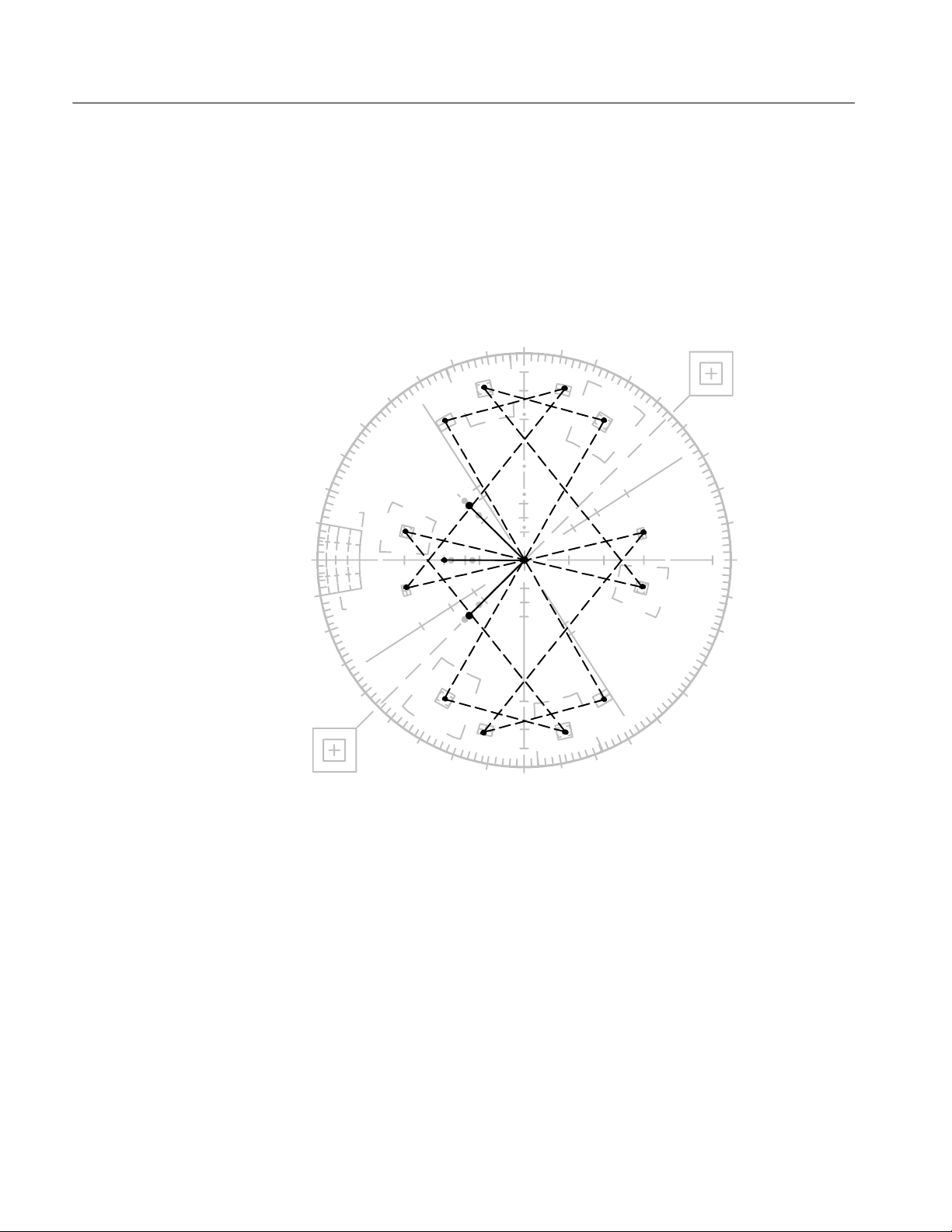
Chrominance. Chrominance is measured in terms of hue and amplitude. Hue is
the attribute of color perception that determines whether the color is red, blue,
green, etc. White, black, and gray are not considered hues. Hue is presented on
the vectorscope crt as a phase angle and not in terms of wavelength. For
example, red, having a wavelength of 610 millimicrons, is indicated as 104° on
the standard color phase vector diagram when the burst is at 180° for NTSC or
135° for PAL. The standard color phase vector diagram is shown in Figure 2-9
for NTSC and Figure 2-10 for PAL.
R-Y
RED
90°
104°
YELLOW
167°
123°
I
100
80
60
40
20
MAGENTA
61°
33°
Q
BURST
180°
GREEN
241°
CYAN
284°
--I
303°
B-Y
0°
BLUE
347°
Figure 2-9: NTSC standard color phase Vector diagram.
2- 16
1720/1721
Page 45
Operating Instructions
45°
45°
0.4
0.2
--0.2
--0.4
iV
CYAN
F
MAGENTA
a
0.2
-- a
CYAN
BLUE
BLUE
MAGENTA
F*
U
F=U+iV
F*=U--iV
RED
GREEN
YELLOW
--0.2
YELLOW
GREEN
RED
Figure 2-10: PAL standard color phase Vector diagram.
Saturation is the degree to which a color (or hue) is diluted by white light in
order to distinguish between vivid and weak shades of the same hue. For
example, vivid red is highly saturated and pastel red has little saturation.
Because saturation is a product of both luminance and chrominance amplitudes,
and a vectorscope can only measure chrominance amplitude, the radial distance
from the center to the end of the color vector is chrominance amplitude. If burst
vector amplitude corresponds to the 75% amplitude marking (see Figure 2-11 for
NTSC and Figure 2-12 for PAL), the colors represented by the vectors when they
are within the targets are of 75% amplitude.
1720/1721
If burst vector amplitude corresponds to the 100% marking and the chrominance
vectors are within the target, the color amplitude is 100%.
2- 17
Page 46

Operating Instructions
dᡢ
10°
0°
10°
20%
dG
10%
dG
YL
yl
75% 100%
WITH
SETUP
75%
100%
WITHOUT
SETUP
Figure 2-11: Partial 1720 graticule showing the 75% amplitude burst target, with and
without setup compensation.
Encoding. The hue and color amplitude information in the color television
system is carried on a single subcarrier frequency: 3.579545 MHz for NTSC and
4.43361875 MHz for PAL. These signals, in modulated subcarrier form, are
called chrominance. The hue information is carried by the subcarrier phase; the
color amplitude information is carried by means of amplitude modulation with
the subcarrier suppressed. A subcarrier which supplies phase information is
required for demodulation. No picture chrominance signals are present during
the horizontal blanking interval and a sample of the subcarrier, used by decoders
for a reference (called burst), is provided within this interval.
2- 18
dᡢ
10°
0°
10°
20%
dG
10%
dG
YL
75% 100%
75% AMPLITUDE
BURST TARGETS
yl
100%
75%
Figure 2-12: Partial 1721 graticule showing the 75% amplitude burst target.
1720/1721
Page 47

Operating Instructions
Decoding. To recover the hue information, phase demodulators are employed in
the vectorscope. The phase reference is the color subcarrier, which is regenerated by an oscillator in the instrument. The oscillator is locked in both phase and
frequency to the incoming color burst signal. The vectorscope displays the
relative phase and amplitude of the chrominance signal on polar coordinates. To
identify these coordinates, the vector graticule (see Figure 2-11 for NTSC and
Figure 2-12 for PAL) has points that correspond to the proper phase and
amplitude of the three primary colors and their complements, which are related
to the 180° burst vector for NTSC and the 135° burst vector for PAL. The
coordinates for the primary colors (red, blue, and green) and their complements
(cyan, yellow, and magenta), when the burst vector is at 225° for PAL, are
identified with lower case abbreviations.
Any errors in the color encoding, video tape recording, or transmission processes
which change these phase or amplitude relationships causes color errors on the
television receiver picture. The polar-coordinate-type of display, such as that
obtained on the 1720/1721, has proven to be the best method for portraying these
errors.
Functional Use of the Vector Graticule
Measurement of Color
Bars
The polar display permits measurements of hue in terms of the relative phase of
the chrominance signal with respect to the color burst. Relative amplitude of
chrominance to burst is expressed in terms of the displacement from center
(radial dimension of amplitude) towards the color point which corresponds to
75% (or 100%) amplitude for the color being measured.
On the 1720 graticule, each chrominance vector terminates in a system of
graticule targets in the form of two boxes (a small box inside a large box). See
Figure 2-13. The dimensions of the large boxes represent ±10° centeredonthe
exact chrominance phase, and ±20% of chrominance amplitude centered around
100% of standard amplitude. The dimensions of the smaller boxes represent
±2.5° and ±2.5 IRE.
1720/1721
2- 19
Page 48

Operating Instructions
MG
20%
60.68°
2.5°
2.5°
50.68°
20%
Q
b
U
50°
40°
30°
20°
10°
cy
2.5 IRE
10°
70.68°
10°
Figure 2-13: Fine detail of the 1720 graticule magenta target.
On the 1721 graticule, each chrominance vector related to the +V burst
terminates in targets that are in the shape of two boxes (a small box inside a large
box). See Figure 2-14. The large box represents ±10° centered on the exact
chrominance phase and ±20% of chrominance amplitude centered around 100%
standard amplitude. The dimensions of the inner target represent ±3° and ±5%
of chrominance amplitude; the vectors associated with the --V burst terminate in
the smaller targets.
2- 20
1720/1721
Page 49

Operating Instructions
MG
20%
60.65°
3°
3°
50.65°
20%
Q
b
U
50°
40°
30°
20°
10°
cy
10°
70.65°
5%
10°
Figure 2-14: Fine detail of the 1721 graticule target.
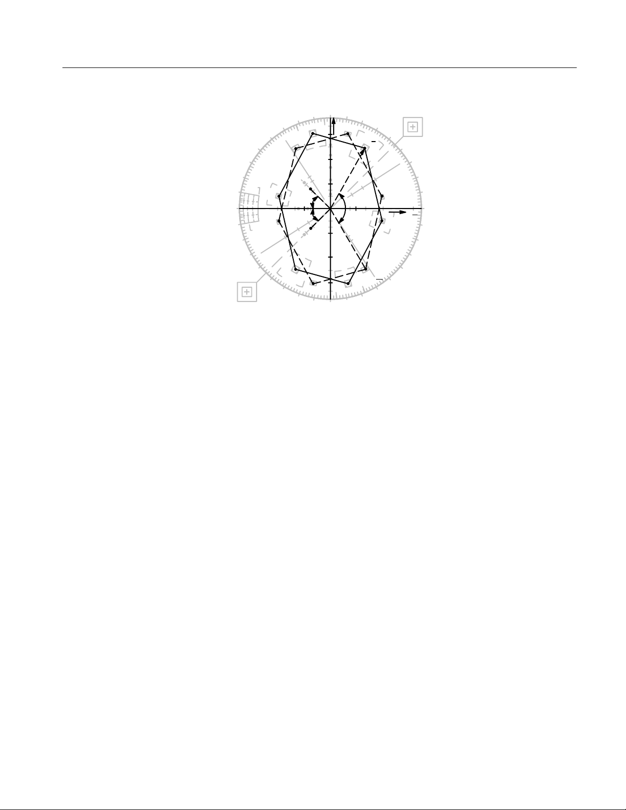
On the 1720, the small marks at intervals along the I and Q axes denote the
amplitudes of the chrominance components (see Figure 2-15). On the 1721, the
small marks at intervals along the U and V axes denote the amplitudes of the U
and V chrominance components (see Figure 2-16).
R--Y
+I
123°
I
90°
R
MG
+Q
33°
Q
BURST
180°
YL
B--Y
0°
B
-- Q
213°
G
CY
270°
-- I
303°
Figure 2-15: Simulated 1720 graticule showing the relationship between amplitudes
on the I and Q modulation axes and the location of the color vector targets.
1720/1721
2- 21
Page 50
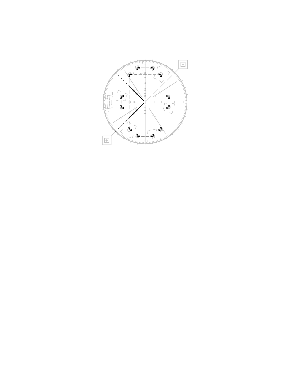
Operating Instructions
V
90°
+V BURST
135°
R
g
cy
MG
Q
mg
b
U
0°
B
180°
--V BURST
225°
YL
yl
G
r
CY
270°
Figure 2-16: Simulation of a 1721 graticule showing the relationship between
amplitudes on the U and V axes and the locations of the color vector targets.
The horizontal and vertical axes of the vector graticule contain markings for
checking Vector Mode bandwidth. A subcarrier frequency sine wave whose
amplitude places it on the outer compass rose is used as a reference. When the
frequency is changed the diameter of the circle should reduce. At a point equal
to 70% of full amplitude (3 dB), there are gaps in the horizontal and vertical
axes. This calibration aid makes it possible to check the --3 dB points of the
demodulator output amplifiers.
Differential Gain and
Phase Measurements
2- 22
The two major distortions that affect the signal are differential gain and
differential phase. They are chrominance non-linearities caused by luminance
amplitude variations. Both can be measured on the vectorscope. Differential
gain is a change in color subcarrier amplitude due to a change in the luminance
signal while the hue of the original signal is held constant. In the reproduced
picture, saturation will be distorted in the areas between the light and dark
portions of the scene. Differential phase is a phase change of the chrominance
signal, caused by a change in the luminance signal, while the original chrominance signal amplitude is held constant. In the reproduced picture, the hue will
vary with the scene brightness. Differential gain and differential phase may
occur separately or together.
1720/1721
Page 51

Operating Instructions
dᡢ
10°
0°
10°
20%
dG
10%
dG
YL
yl
75% 100%
WITH
SETUP
75%
100%
WITHOUT
SETUP
Figure 2-17: A simulation of a part of the 1720 graticule showing the differential
phase and gain measurement scales with approximately 10° differential Phase (dP).
Differential gain (dG) and differential phase (dφ) measurements can be made
using the graticule markings located at the outer edge of the B-Y axis (1720) or
--U axis (1721). See Figure 2-18 for a differential gain measurement illustration
and Figure 2-17 for a differential phase measurement illustration.
High Resolution Differential Phase Measurement ---- The DEMOD OUT from
the 1720/1721 can be used to drive one of the inputs to a 1730-Series Waveform
Monitor for improved measurement resolution. This measurement requires a
modulated ramp or staircase signal with the 1720/1721 gain normalized so the
chrominance amplitude is on the compass rose.
1720/1721
The 1730-Series must have the DC REST OFF and the VERTICAL GAIN at
X5. Once these conditions are set up, using 1 LINE SWEEP makes each major
vertical division of the 1730-Series graticule equal to 2°, when referenced to the
sweep origin.
2- 23
Page 52

Operating Instructions
X Y Measurements
dᡢ
10°
0°
10°
20%
dG
10%
dG
YL
75% 100%
75% AMPLITUDE
BURST TARGETS
yl
100%
75%
Figure 2-18: Simulation of the 1721 Differential Gain and Phase graticule showing
approximately 10 % differential Gain (dG).
Any oscilloscope, including vectorscopes that have identical X and Y amplifiers,
can be used to make accurate stereo audio phase measurements. When identical
signals of equal amplitude are input, the resultant display will be a lissajous
pattern, whose opening is relative to the phase error between the signals. If there
is no phase error between signals, the display will be a diagonal line, at a 45°
angle. When the signals are not equal in phase, the pattern will have its axis on
the diagonal but be displayed as an ellipse. As long as the amplitude of the
signals remains the same, the amount of opening in the ellipse (up to 90°)isa
relative measure of the phase difference. At 90° the display is a circle; errors
greater than 90° cause the axis to rotate by 90°.
Making Stereo Audio
Phase Measurements
2- 24
The graticule for the 1720/1721 has scales for measurement of stereo audio
phase. The dashed diagonal line is the measurement axis for errors less than 90°,
it is terminated in amplitude targets that correspond to the length of X and Y
axes. The boxes, surrounding the crosshairs, are equal to amplitude errors of 1/2
and 1 dB, respectively.
The upper half of the Y axis has markings, in 10° increments, for measurement
of the elliptical waveform that occurs when there is a phase error. Both the X
and Y axes have --3 dB markings making it easy to check the bandpass of the
amplifiers. The 3 dB points are minor breaks in the line about 30% of the
distance from the graticule circle to the graticule center.
In order to make this type of measurement it is essential that the input signal
amplitudes be equalized. This is easily accomplished by applying only one
1720/1721
Page 53

Operating Instructions
signal at a time and adjusting its gain to correspond to the appropriate axis
(horizontal to the X axis and vertical to the Y axis).
Once both signal gains are normalized they can be displayed in the XY Mode
and the relative stereo phase measured.
Looking at Incidental
Carrier Phase Modulation
The High-Gain X and Y inputs of the 1720/1721 can be used to look at ICPM
(Incidental Carrier Phase Modulation). ICPM is a change in carrier phase with a
signal level change. It will show up as apparent differences between measurements made in synchronous and envelope detection modes. On home receivers,
with envelope detectors, the picture will be uneffected if the visual transmitter
has been adjusted using envelope detection when there is appreciable ICPM.
However, ICPM can show up in the home receivers audio as intercarrier buzz.
ICPM can be looked at by applying the Video and Quadrature Outputs from a
demodulator to the 1720/1721 X and Y Inputs. The Quadrature Output drives
the High-Gain X Input and the Video Output drives the High-Gain Y Input. The
resulting display will be vertical when ICPM is minimum, and tilted when ICPM
is present.
NOTE. This is not a definitive measurement, but does provide a way of
determining if ICPM is present in the signal.
1720/1721
2- 25
Page 54

Operating Instructions
2- 26
1720/1721
Page 55

Warning
The following servicing instructions are for use only by qualified personnel. To
avoid personnel injury, do not perform any servicing other than that contained in
the operating instructions unless you are qualified to do so. Refer to General
Safety Summary and Service Safety Summary prior to performing any service.
Page 56

Page 57

Service Safety Summary
Only qualified personnel should perform service procedures. Read this Service
Safety Summary and the General Safety Summary before performing any service
procedures.
Do Not Service Alone. Do not perform internal service or adjustments of this
product unless another person capable of rendering first aid and resuscitation is
present.
Disconnect Power. To avoid electric shock, switch off the instrument power, then
disconnect the power cord from the mains power.
Use Care When Servicing With Power On. Dangerous voltages or currents may
exist in this product. Disconnect power, remove battery (if applicable), and
disconnect test leads before removing protective panels, soldering, or replacing
components.
To avoid electric shock, do not touch exposed connections.
1720/1721
S- 1
Page 58

Service Safety Summary
S- 2
1720/1721
Page 59

Installation
Page 60

Page 61

Section 3 Installation
Packaging
Electrical Installation
Power Source
Mains Frequency and
Voltage Ranges
Operating Options
The shipping carton and pads provide protection for the instrument during
transit, they should be retained in case subsequent shipment becomes necessary.
Repackaging instructions can be found in Section 6 (Maintenance) of this
manual.
This instrument is intended to operate from a single-phase power source with
one current-carrying conductor at or near earth-ground (the neutral conductor).
Only the Line conductor is fused for over-current protection. Systems that have
both current-carrying conductors live with respect to ground (such as phase-tophase in multiphase systems) are not recommended as power sources.
All members of the 1700-Series instrument line operate over a frequency range
of 48 to 66 Hz, at any mains voltage between 90 Vac and 250 Vac. These newer
versions of the 1730-Series instruments do not require any internal changes to
select their operating voltage range.
Not all installations are identical. In order to make operation of the 1720/1721
Vectorscope as flexible as possible there are internal jumpers that can be changed
to provide operating flexibility. For example, it is possible to select CW
Subcarrier for EXT REF instead of Composite Video or Black Burst. The
factory preset position is indicated by a box printed on the etched circuit board.
Table 3--1 details these internal jumper selections. Be sure that all operators are
aware of changes, to prevent unnecessary trouble reports, if any of these jumpers
are placed in the optional position. See Figure 3-1 for location of the internal
plug jumpers.
X Y INPUT Connector
1720/1721
The rear-panel XY INPUT connector is a 15-pin, sub-miniature, D-type
connector that provides input to the Horizontal and Vertical (X and Y) Amplifiers. They are balanced (differential), dc-coupled, high impedance (>20 kΩ),
unterminated inputs provided for audio applications. If ac coupling is desired,
external capacitors are required. These inputs are factory calibrated for 0 dBm in
600Ω but can be adjusted for any 600Ω system between 0 and 12 dBm. See
Figure 3-2.
3- 1
Page 62

Installation
A3 Main Bd
Front
Figure 3-1: Plug jumper locations. A small arrow on the board, next to the plug
jumper, denotes pin 1.
Table 3- 1: Internal Jumper Selection
Jumper
Number
Name Position Purpose
J245 Blanking disable
J696 Ext sync source
1
1
J796 Subcarrier refJ921 X High gainJ920 Y High gain
A3J696 External Sync Source (EXT REF Input) 1-2 EXT REF (factory preset)
Converted to CW Subcarrier Input 2-3 CH-A INPUT
A3J796 Subcarrier Reference 1-2 EXT REF (factory preset)
2-3 CW Subcarrier applied to EXT REF INPUT
A3J920 Y Input High Gain Out Balanced 600Ω input (factory preset)
In Single-ended high gain mode
A3J921 X Input High Gain Out Balanced 600Ω input (factory preset)
In Single-ended high gain mode
A3J245 Blanking Disable Out Normal Blanking (factory preset)
In CRT Blanking disabled
A3A1 J100 Light Enable 1-2 Lights Enabled (factory preset)
2-3 Lights Disabled
3- 2
1720/1721
Page 63

Installation
Not
Used+YInput
+Y
High gain
input
15
GND
14
-- Y
Input
678
GND
13
-- Y
Input
5
12
GND
Input
234
GND
GNDGND
+Y
High gain
input
+Y
-- Y
Input
1
91011
-- Y
Input
Figure 3-2: Rear panel XY INPUT connector showing pins with their functions.
0 dBm is equal to 1 mW or 2.19 V peak-to-peak in 600Ω.
12 dBm is equal to 15.8 mW or 8.72 V peak-to-peak in 600Ω.
Inputs can be driven single-ended by driving either the + or -- X and Y inputs
with the opposite polarity inputs grounded.
In addition, a single-ended, high-gain mode can be used for other, primarily
non-audio, applications. It can be accessed by installing plug jumpers on J920
and J921 (on the Main board, see Table 3--1) and inputting the signal on the +X
and +Y inputs with the --X and --Y inputs grounded.
Auxiliary Connector
1720/1721
The rear-panel AUXILIARY connector is a 9-pin, D-type connector. It is used to
control the display from a companion 1730-Series Waveform Monitor. Line and
Field selection information is provided to the vectorscope over the bus that is
contained in this interface. Figure 3-3 and Table 3--2 show the AUXILIARY
connector pin assignments.
3- 3
Page 64

Installation
Ground
45
89
TXD RXD External
strobe out
Ground
123
67
Figure 3-3: View of the 1720/1721 rear panel showing AUXILIARY connector pins
with their functions.
Table 3- 2: AUXILIARY Connector Pin Assignments
Pin # Use
2-3-4-6 No connection.
1-5 Ground.
7 External Strobe In for Line Select blanking.
Mechanical Installation
Cabinetizing
8 RXD (Receive Data) 1730-Series communication to the 1720/1721.
9 TXD (Transmit Data) 1720/1721 return communication to 1730-Series.
All qualification testing for the 1720/1721 was performed in a 1700F00 cabinet.
To guarantee compliance with specifications, the instrument should be operated
in a cabinet. The plain cabinet, 1700F00, is shown in Figure 3-4.
The portable cabinet, 1700F02, is shown in Figure 3-5. The 1700F02 has a
handle, four feet, a flip-up stand, and a front cover. This F02 cabinet is compatible with the TEKTRONIX BP1 battery pack, which can be used as a dc power
source. The hole sizes and spacing are different from those of the 1700F00.
All of the 1700-Series metal cabinets, which are available from Tektronix as
Optional Accessories, provide the proper electrical environment for the
instrument. They supply adequate shielding, minimize handling damage, and
reduce dust accumulation within the instrument.
3- 4
1720/1721
Page 65

8.250
Installation
0.688
5.105
1.060
16.180
6.875
Rear
0.156 Dia (4)
6.130
12.725
Bottom Side
Figure 3-4: 1700F00 plain cabinet.
1720/1721
3- 5
Page 66

Installation
8.250
0.688
5.105
1.625
16.180
6.875
Rear
5.000
Bottom Side
0.141 Dia (4)
9.435
3.310
Securing the Instrument in
its Cabinet
Figure 3-5: 1700F02 portable cabinet.
WARNING. Cabinet Mounting Screws
Do not attempt to carry a cabinetized instrument without installing the mounting
screws. Without the mounting screws there is nothing to hold the instrument in
the cabinet if it is tipped forward.
The instrument is secured to the cabinet by two 6-32 Pozidrive® screws, located
in the upper corners of the rear panel. See Figure 3-6.
3- 6
1720/1721
Page 67

Cabinet Securing Screws
Figure 3-6: Cabinet securing screws.
Installation
Rack Mounting
The optional 1700F05 side-by-side rack adapter, shown in Figure 3-7, consists of
two attached cabinets. It can be used to mount the 1720/1721 and another
half-rack width instrument in a standard 19-inch rack.
18.970
Mounting
holes
6.875
17.270
5.250
1720/1721
Rear view
Figure 3-7: 1700F05 rack adapter.
The rack adapter is adjustable, so the 1720/1721 can be more closely aligned
with other equipment in the rack. See Figure 3-8.
3- 7
Page 68

Installation
Handle bracket is attached
at this setting when shipped.
To mount 1700-Series half-rack
instruments even with other
Tektronix Television equipment.
To mount 1700-Series half-rack
instruments, WFM-300A, and 760
even with 528A or 1420-Series.
To mount 528A and 1420-Series.
Figure 3-8: 1700F05 rack adapter adjustment.
If only one section of the rack adapter is used, a 1700F06 Blank Panel can be
inserted in the unused section. See Figure 3-9. The rack adapter and panel are
available through your local Tektronix field office or representative.
1700F05
1700F06
3- 8
Figure 3-9: 1720/1721 and 1700F06 blank panel.
1720/1721
Page 69

Installation
Custom Installation
For applications such as consoles, the instrument can be mounted with front
molding flush or protruding from the console. In both cases, allow approximately 3 inches of rear clearance for BNC and power-cord connections.
To mount the 1720/1721 safely, attach it to a shelf strong enough to hold its
weight. Install the mounting screws through the four 0.156-inch diameter holes
in the bottom of the 1700F00 cabinet. See Figure 3-10.
For Flush Front Panel: Cut hole the same size as
the monitor front molding to allow the monitor front
panel to align with the custom panel surface.
Requires four 0.156”
holes below the 1700F00
cabinet to secure the
instrument to the shelf.
For Protruding Front Molding:
Cut hole in panel the same size
as the opening in the monitor
cabinet to allow the front panel
molding to cover the hole.
Figure 3-10: Typical custom installation showing the console.
1720/1721
3- 9
Page 70

Installation
3- 10
1720/1721
Page 71

Theory of Operation
Page 72

Page 73

Section 4 Theory of Operation
The material in this section is subdivided into general description, which is
supported by the main block diagram and simplified block diagrams, and
detailed circuit descriptions that use the schematic diagrams as illustrations. A
thorough understanding of the instrument starts with a knowledge of how the
major circuit blocks fit together, which is then followed up by knowledge of the
individual circuit functions.
Overview
The simplified block diagram shown in Figure 4-1 and the following paragraphs
are intended to introduce the 1720/1721 Vectorscope in the broadest of terms. A
full scale discussion of operation follows this overview.
The 1720/1721 is a special purpose oscilloscope, designed to display the
variations of phase in the NTSC or PAL color television signal. Color signals,
input through the rear-panel bridging loop-through connectors, are displayed on
the crt in a Cartesian plot. An added feature makes it possible to compare
two-channel audio signals. Audio signals are brought in through the rear-panel
X Y INPUT connector for an XY display of phases used for stereo encoding of
the audio signal.
1720/1721
Front-panel mode switching is accomplished by push-button switches whose
status is being constantly polled by a Microprocessor. The Microprocessor
controls gains and switching functions to make specific measurements.
The composite video signal from either the Channel A or B input is first
separated into its chrominance and luminance components. The luminance
component is used to generate the clamp signals used in the display of the
chrominance information and for synchronizing vectorscope operation. The gain
of the chrominance signal is adjusted prior to input to the Demodulators, for
quadrature demodulation. The demodulated output is filtered and clamped (at
H-Sync rate) by clamped amplifiers. The Output Amplifiers match signal
impedance and drive the crt deflection plates.
In addition to being demodulated and displayed, the chrominance signal can be
used to provide the internal subcarrier sample (in the INT REF position) to the
Subcarrier Regenerator; External Reference, when selected, is through the
rear-panel bridging loop-through EXT REF input. The regenerated subcarrier
can be phase shifted, by up to 360°, using the front-panel PHASE control. For
PAL applications, a 180° flip-flop is employed to reverse the phase of every
4- 1
Page 74

Theory of Operation
Block Diagram
other line so that the +V and --V signals can be overlaid for phase matching
applications.
The regenerated subcarrier, used for demodulation, is applied directly to the B--Y
(U) Demodulator and delayed by 90° (quadrature phased) for the R--Y (V)
Demodulator. The B--Y (U) Demodulator drives the Horizontal Output
Amplifier; the R--Y (V) Demodulator drives the Vertical Amplifier.
The rear-panel X Y INPUT connector provides an input for audio signals, which
can be displayed as XY signals for stereo comparisons. Identical amplifiers
provide high input impedance and drive the Vertical and Horizontal Output
Amplifiers.
If there is no signal, the Center Dot Blanking circuit blanks the crt to prevent it
from being damaged by the non-deflected center dot.
This description uses the 1720/1721 Block Diagram, which is located at the
beginning of the Diagram section (Section 9). The diagram can be folded out
and viewed while reading this description.
Video Input
Luminance Processing
Microprocessor
Video signals are input through identical input amplifiers to normalize gain and
provide impedance matching. An external reference can be used for both
luminance- and chrominance-related functions. If composite video or black burst
is used for the External Reference, no additional processing is required. When
CW Subcarrier is used, the luminance reference is taken from the video input,
and the chrominance reference is attenuated from the subcarrier input through the
External Reference.
The sync signals used by the vectorscope are contained in the luminance
information from the video inputs. The composite video signal through the
Luminance Amplifier drives a sync separator, whose output is used to drive a
Bowes Oscillator that regenerates H Sync. The H Sync also generates Sample
Pulses and the Clamp signals, that activate the Burst Switches, and provide the
line rate control signal for the V-Axis Switcher.
The Microprocessor polls the front panel to determine changes in status. Current
status is stored in Nonvolatile Random Access Memory (NOVRAM), which
makes it possible to return to the same front-panel condition should power be
interrupted. If the 1720/1721 is being used as an auxiliary instrument to a
1730-Series Waveform Monitor, any stored vectorscope front-panel setup data is
also in the NOVRAM. Based on the front-panel conditions, the Microprocessor
generates controlling signals that are used throughout the 1720/1721. The
4- 2
1720/1721
Page 75

X Input
Y Input
Theory of Operation
front-panel indicators are driven by the Microprocessor so that they will mirror
the current measurement criteria.
CH A
CH B
EXT REF
Gain
Sync
stripper
180°
Flip
90°
Subcarrier
regenerator
generator
Figure 4-1: Simple block diagram of a 1720/1721 Vectorscope.
Phase
shifter
Clamp
Detectors
Center dot
blanking
To C RT
Verti cal
deflection
plates
To C RT
Horizontal
deflection
plates
To C RT
Blanking
Gain Cell
Chrominance Processing
1720/1721
The gain cell uses front-panel VAR GAIN and GAIN CAL settings and
switching signals from the Microprocessor to adjust the chrominance gain prior
to demodulation. Gain cell chrominance is clamped to ground at sync tip time
for a stable reference level.
Chrominance from the incoming video signal, either internal or from the
External Reference, is conditioned by the Chrominance Amplifier and applied to
the Phase Detector at burst time (Burst Gate signal). The chrominance input to
4- 3
Page 76

Theory of Operation
the Quad Phase Detector is delayed by 90°. The chrominance signal is compared
to the regenerated subcarrier from the VCXO with the output low-pass filtered
and buffered. The Phase Detector output is clamped and supplied to the Error
Amplifier, which provides an output voltage to correct the VCXO should it be
off frequency.
The Quad Phase Detector compares the burst chrominance to 90° phase-shifted
subcarrier, with the output low-pass filtered and buffered. The resulting signal is
a pulse, when burst is present, that clamps the Phase Detector output. It is also
checked for phase lock and, if unlocked, an output is supplied to the Error
Amplifier to increase its bandwidth for a faster locking. When the TEST (Cal
Mode) is enabled, the Error Amplifier is forced into an unlocked state to provide
the test circles.
The regenerated subcarrier from the VCXO can be phase shifted up to 360° by a
goniometer (front-panel PHASE control) whose output is buffered prior to input
to the Demodulators. The amplitude of the regenerated subcarrier is fed back to
the VCXO through an Automatic Gain Control circuit.
The V-Axis Switcher takes the output of the Phase Detector H Sync and
generates an alternate line signal. The resulting alternate line signal is used to
control the input switching to the Quad Phase Detector. In PAL (1721)
instruments, an additional signal, from the Microprocessor, is used by the V-Axis
Switcher to control the Quad Phase input to the R--Y Demodulator.
Demodulators
Output Amplifiers
CRT Blanking
The 1720/1721 employs quadrature demodulation, which consists of delaying
the regenerated subcarrier by 90° to the R--Y (U) Demodulator. In the 1721, an
additional 180° phase shift is achieved by switching the regenerated subcarrier to
the --input of the demodulator. The incoming chrominance is compared to the
regenerated subcarrier and the output is low-pass filtered and amplified. Center
Dot clamping is used to keep the effects of chrominance from distorting the
display center dot.
The Vertical and Horizontal Deflection Amplifiers do double duty. They are
used to output both the vector display and the XY display. The input of the
amplifiers is checked for the presence of a signal over a certain amplitude, and
the resulting output is one input to the CRT Blanking circuit. X and Y signals
are input through balanced amplifiers, that can be converted to single-ended high
gain inputs. Input switching is controlled by the Microprocessor and front-panel
switching.
CRT blanking takes inputs from the front-panel INTENSITY control, the
Microprocessor, and the Center Dot Comparators to generate the blanking signal.
In addition, in the Auxiliary mode of operation, a line select strobe from a
companion 1730-Series can drive the blanking amplifier to unblank only the line
or lines that are selected with the waveform monitor’s line selector.
4- 4
1720/1721
Page 77

Circuit Descriptions
The following descriptions are divided by diagram number and then further
subdivided by logical circuit blocks. The descriptions follow the order of the
diagrams in Section 9. Individual diagrams can be folded out and consulted
while studying these descriptions.
DIAGRAM 1 INPUT AND DEFLECTION AMPLIFIERS
CH A
Theory of Operation
CH-A
CH-B
EXT REF
CH B
EXT REF
VIDEO
Gain
cell
GAIN CAL
CHROMA
VARIABLE
Video signal input to the 1720/1721 Vectorscope is through high-impedance
bridging loop-through inputs. Gain is normalized by the Input Amplifiers prior
to being input to the Gain Cell. The amount of amplification provided by the
Gain Cell is controlled by the Gain Cal, Variable, and the choice of 75% or
100% amplitude color bars.
The External Reference input is also a high impedance bridging loop-through,
which is dc coupled to a unity gain operational amplifier.
Video Input Amplifiers
1720/1721
The Channel A and Channel B input buffers are ac coupled (C199 and C497),
grounded base amplifiers with Q297 and Q493 as the active elements. Q391 is a
saturating switch that shunts current away from the Channel B input when
Channel A is being displayed. Q296 serves the same purpose when Channel B is
being displayed. R594 and C198 are adjustments that match the phases and
gains of Channel A and Channel B. They modify the input resistance of
Channel B and the input capacitance of Channel A. Signal current flows through
either CR297 or CR496 (depending on channel selection) into the summing
4- 5
Page 78

Theory of Operation
junction of a differential amplifier (Q293 and Q292) that drives the Output
Amplifier (Q192). The feedback resistor that sets the gain is R293.
The External Reference Input Amplifier is nearly identical to the channel inputs
and provides a signal to the reference switch. R994 is the input resistor and
R992 is the feedback resistor, the combination of which sets the gain to 1.
Gain Cell
The Gain Cell, whose output is chrominance, consists of U184, U383, Q385, and
Q490. A band-pass filtered (L185 -- C185) signal is fed into pin 6 of U184.
U184 consists of a current source, differential amplifier pair, and a pair of
transistors connected as diodes. U383 consists of four transistors connected in a
cross-coupled gain cell arrangement with a transistor used as a heater to keep
U383 at the same temperature as U184. The diode-connected pair in U184 is a
current-to-voltage converter that drives the gain cell transistors in U383. U380 is
an operational amplifier that drives the gain port of the Gain Cell. U274 is a
Microprocessor-controlled switch that enables the Variable Gain, Gain Cal, and
the 75% or 100% color bar amplitude gain settings.
DIAGRAM 2 SUBCARRIER REGENERATOR
L
CHRM
Ext ref
video
C
Sync
separator
Back
porch
sample
Bowes
osc
Quad
phase
detector
H
H
4- 6
To phase
shifter
Voltage
controlled
oscillator
Loop
phase
detector
E
Burst
clamp
Incoming signal, from the Input Amplifiers, is amplified and fed to the Luminance and Chrominance Amplifiers. Output of the Luminance Amplifier drives
the Sync Separator, which generates the H Sync used throughout the Vectorscope, and the Back Porch Sample that enables the Phase Lock Loop.
1720/1721
Page 79

Theory of Operation
Burst ref
Burst amp
Phase
detector
Burst
demod
Burst
gate
Loop filter
Phase
control
Subcarrier
oscillator
VCO
Figure 4-2: Block diagram of the Phase Lock Loop.
The heart of the Subcarrier Regenerator is a phase lock loop. See Figure 4-2.
The Subcarrier Oscillator (VCXO) is a voltage-controlled oscillator that freeruns
near the reference subcarrier frequency. The Burst Demodulator is a mixer that
detects phase differences between the reference input and the Subcarrier
Oscillator during burst time. The difference output is an error signal proportional to the phase difference detected.
The error signal drives the Phase Lock Control, which is a low-pass filter to
remove high-frequency ac components in the error signal. The filter has two
bandwidths, a wide one to search for the unlocked signals, and a narrow one to
maintain stable phase lock once the signal has been captured.
Reference Switch
The Phase Lock Control loop filter completes the loop by controlling the
Subcarrier Oscillator. If the input reference changes, the oscillator will follow.
For the 1721, the PAL Phase Lock Control block samples every burst.
U889 is a Quad CMOS switch that selects the appropriate input signal for the
Sync Separator and the Subcarrier Regenerator. In normal operation, both the
sync and subcarrier sources follow the front-panel Reference switch and are
driven by A or B when Internal is selected, or by the EXT REF input when
External is selected. When J696 is in the 2 and 3 position, the Sync Separator is
always driven by the A or B input, even when External Reference is selected.
This mode should be used if CW Subcarrier is used as the Reference for a
composite video input signal. It will ensure that the clamp pulses are synchronous with the incoming video.
The two remaining switches in U889 allow the reference signal to pass to the
Subcarrier Regenerator only during burst time. In NTSC, with W986 installed,
the two switches both close during every back porch, allowing every burst to
pass to the two phase detectors. In PAL, with W987 installed and U986
removed, the Loop Phase Detector, U646, receives every burst and the Quadrature Phase Detector, U854, receives every other burst.
1720/1721
4- 7
Page 80

Theory of Operation
Luminance and
Chrominance Amplifiers
Sync Separator
The reference signal is ac-coupled through a tuned circuit, C791 and L791, to
drive the Chroma Amplifier, Q794 and Q795. Luminance is removed and in
normal operation the chrominance is amplified by about three times. With J796
in the 2 and 3 position (External CW Subcarrier input), the gain is changed to
slightly less than one.
The reference signal is dc-coupled to the inverting Luminance Amplifier, Q693,
which has unity gain and removes much of the chrominance. The collector of
Q693 drives the Sync Separator.
The Sync Separator strips off and processes the sync from the luminance signal
to control the timing circuitry. The Sync Stripper receives its input through
C685 and R686 into the base of Q685, a summing junction. Q685 and Q680
form an operational amplifier that inverts the sync signal and clips it near the
sync tip. Amplifier gain, which is high at sync tip time, is set by the combination of R686 (R
and CR681 are both on, shunting Q680 to reduce amplifier gain and limit
saturation so that the response to the next sync transition will be rapid.
During sync time a clamp circuit consisting of Q681 and Q688 maintains the
output of the operational amplifier at about +5 V. The output is fed back to
maintain the proper level. Q681 and CR682 are a current source that is on
during sync tip. At the end of sync time, when Q680 goes low, CR682 is pulled
down and Q681 shuts off.
) and R682 (Rf). During non-sync time (active video) CR680
i
Bowes Oscillator
Back Porch Sample
Loop Phase Detector and
Amplifier
Q780 outputs negative-going sync that has any remaining noise greatly reduced.
The output of Q780 is fed back, through CR781, to the clamp circuit, Q688.
The Bowes Oscillator, Q880 and Q781, is triggered by the leading edge of sync.
It accepts triggers only at H intervals, during the vertical interval, to avoid
triggering on the wrong equalizing pulses. In the absence of sync the oscillator
freeruns so that sample pulses are always available for clamping. The output at
the collector of Q781 is negative-going and lasts for approximately 4.5 µsto
provide horizontal sync to the rest of the instrument.
U884A is a one-shot that provides a negative-going pulse at its output (pin 4)
that controls the sampling of burst. It is triggered by the trailing edge of sync
and its Q output (pin 13) is a 4 µs long, positive-going, back porch pulse that is
NANDed with the output of flip-flop U774B, which is clocked at a line rate.
The output of the gate (U876C, pin 8) is a negative-going pulse that occurs every
other back porch.
U646 is the Subcarrier Regenerator (Phase Lock) Loop Phase Detector. It is a
balanced demodulator, whose carrier input is driven by the VCXO CW sine
wave. Its signal input is driven by burst chrominance from the Chroma
4- 8
1720/1721
Page 81

Theory of Operation
Reference Amplifier. The output of this phase detector is an ac multiplication of
the input signals, which occurs only during the time that both of the input signals
are present. The average dc output level is proportional to the difference in
phase between the inputs.
The output is filtered to remove any chrominance and harmonics and drives
U640, which is a non-inverting, high-gain operational amplifier.
Quadrature Phase
Detector and Amplifier
Burst Clamp
Lock Detector and
Bandwidth Switch
The Quadrature Phase Detector is similar to the Loop Phase Detector, except that
the carrier input signal is phase shifted by 90° by a network consisting of L750,
C548, and R647. This results in the output of the Quadrature Phase Detector
being maximum when the output of the Loop Phase Detector is zero. Since
Loop Phase Detector output is zero (phases are matched) during burst, the
Quadrature Phase Detector provides a large-amplitude pulse occurring only
during burst time. Q732 inverts and amplifies the output pulse to drive the Burst
Clamp and Lock Detector.
At burst time, C738 is charged by current through R734. The direction and
amount of current is determined by the output of the Loop Phase Detector
Amplifier, U640, with respect to ground (through R734 and Q733). The voltage
developed across R734 is the input voltage seen by the Error Amplifier.
The Subcarrier Regenerator has two different bandwidths. Wide bandwidth is
for fast lock-up and a large pull-in range. Once locked, the loop goes into a
narrow-bandwidth mode, which provides a stable reference with very little phase
jitter.
Q836 is turned on at every burst pulse, keeping C737 discharged and the output
of U734B at a low level. If burst is missing or not locked, Q836 is off during
burst time and C737 charges slowly negative until the output of U734B is high
enough to turn on the Bandwidth Switch transistor, Q632.
1720/1721
Error Amplifier
Q632 is off when subcarrier is locked to incoming burst. If the subcarrier is not
locked, U734B saturates Q632 and grounds a portion of the Error Amplifier
feedback to allow the Error Amplifier to rapidly change the bias on the VCXO
varicap CR235 and quickly bring the loop back into lock.
U734A is a non-inverting amplifier whose RC feedback network acts as a
low-pass filter to determine the Subcarrier Regenerator loop response. Any input
voltage to U734A is amplified and biases the VCXO varicap, CR235.
The Loop Balance control, R534, adjusts the Phase Locked Loop dc offset so
that there is no phase shift when burst amplitude changes.
4- 9
Page 82

Theory of Operation
PAL Phasing
VCXO
The Subcarrier Regenerator in the 1721 Vectorscope samples alternate lines and
locks to every other burst. Alternate line sampling can be defeated by moving
W987 to the W986 position, but the +V mode may not be properly phased and
there will be more phase jitter.
The Quadrature Phase Detector receives every other burst from the Reference
Switch. When first trying to lock, this may be either a positive- or negative-going, demodulated burst, since U774B has received no phasing information yet.
If the negative bursts are being received, the minus input (pin 3) of the PAL
Phasing Comparator (U348) will be zero on one line with negative-going burst
pulses on the next line. Since the reference voltage, to the comparator (pin 2), is
a positive voltage the comparator output will remain high and the Preset (pin 10)
of U774B will not be affected.
If the positive-going burst pulses are initially being received by the Quadrature
Phase Detector, pin 3 of U348 will be zero during one line and there will be a
positive-going burst pulse on the next line. This positive burst pulse will cross
the comparator threshold and its output will be negative pulses to preset U774B.
The flip-flop will be rephased, and negative-going bursts will be gated to the
Quadrature Phase Detector .
The VCXO is a phase-locked, voltage-controlled, crystal oscillator with
automatic gain control (AGC). It generates a sine wave at subcarrier frequency
(3.579545 MHz for NTSC, 4.433619 MHz for PAL), controlled by crystal Y129
and varicap CR235. The frequency is stabilized by dc feedback from the Error
Amp, U734, which changes the varicap bias when there is a frequency error.
The output is shaped into a sine wave by a Pi filter consisting of C337, L337,
and C336, to drive the Phase Detectors and the Phase Shifter. The Phase Shifter
is a goniometer, which is a variable capacitance device that shifts the phase of
the display through 360°. Subcarrier Amplifier Q434 amplifies the goniometer
output and drives the Chrominance Demodulators and the AGC Amplifier,
Q334.
The subcarrier amplitude at the collector of Q434 is rectified by CR428 and
stored in C328. The dc level on C328 controls the bias of Q222 through Q334 to
correct for any fluctuations in amplitude. The bias current for Q222 is inversely
proportional to the stored level on C328. If the amplitude rises, Q334 reduces
the gain; if the amplitude goes down, the gain increases, thus stabilizing
subcarrier amplitude.
4- 10
1720/1721
Page 83

DIAGRAM 3 DEMODULATOR
VAxis
switcher
Verti cal
position
clamp
Low
pass
filter
Theory of Operation
DEMOD
OUT
R-Y
(V)
V-Axis Switcher
CHROMA
F
SC
Bandpass
filter
Syc tip
chroma
clamp
Quad
phase
Horiz
position
clamp
Low
pass
filter
B-Y
(U)
Incoming chrominance is band-pass filtered, clamped at sync tip time, and
compared to the phase shifted regenerated subcarrier signal for demodulation.
Subcarrier signal is quadrature shifted (90°) before input to the R--Y (V)
demodulator. In addition, for PAL applications, and any time the front-panel
selected Test Circle is enabled, a V-Axis switcher shifts the subcarrier input by
180° for alternate lines.
Output signal from the Demodulators is low-pass filtered and amplified prior to
driving the Horizontal and Vertical Output Amplifiers. The output of the R--Y
(V) Demodulator is also available through the rear-panel Demodulator Output.
The V-Axis Switcher reroutes the V-Axis Demodulator carrier input on alternate
lines. In both the 1720 and the 1721, V-axis switching is enabled when the
TEST function is selected from the front panel. In the 1721, V-axis switching is
also enabled when the +V/PAL switch is in the +V position.
1720/1721
V-axis switching provides a display of the PAL signal that overlays the --V lines
on the +V lines. The resulting display appears as though only the +V signal is
displayed, similar to an NTSC display. This display is used to evaluate relative
differences between the +V and --V lines. This same operation occurs when the
signal is decoded in a PAL television receiver.
The Microprocessor enables V-axis switching by pulling the Preset input of
U774A (a D-type flip-flop) high, which allows the horizontal sync, clock pulses
to toggle its outputs at a line rate. The D input is controlled by another flip--flop,
4- 11
Page 84

Theory of Operation
U774B (on Diagram 2), which has identified the +V lines (for PAL) in the
Subcarrier Regenerator.
The flip-flop outputs drive Q552 and Q553. A high output turns on the
corresponding transistor to shunt the signal at its collector to ground. This
alternately grounds and drives the + and -- carrier inputs on the V Demodulator
with subcarrier to demodulate the --V lines 180° away from the +V lines.
Chrominance
Demodulators
Sync Tip Chrominance
Clamp
Demodulator Output
Filters and Amplifiers
The Chrominance Demodulators, U467 and U659, are double-balanced
demodulators, whose outputs are voltages proportional to the phase difference
between the signal input (pins 1 and 4) and the carrier input (pins 8 and 10). The
signal inputs are driven by chrominance from the Gain Cell (Diagram 1). The
carrier inputs are driven by a continuous sine wave, at subcarrier frequency, from
the Subcarrier Regenerator (Diagram 2). The subcarrier rate sine wave drives the
B--Y Demodulator directly and is delayed by 90° in the Quad Phase circuit
(L451, C451) before driving the carrier input to the B--Y Demodulator. The
V-Axis Switching circuit, when operating, determines which carrier input of the
R--Y Demodulator is driven by subcarrier.
The demodulator gains are set by the R--Y Gain (R460) and the B--Y Gain
(R655). The bias is controlled by the Center Dot Position Clamp circuits. R666
provides a small percentage of the Y signal into the X signal to be used as part of
the orthogonality adjustment.
Q353 is driven to saturation during horizontal sync time, when Q353 is saturated
any residual subcarrier present in the signal is grounded to provide a clean, zero
carrier reference for the demodulator position clamps.
A four-pole, active, low-pass filter (Q564 and Q371 for the R--Y and Q764 and
Q664 for the B--Y) removes the high-frequency components of the demodulation
process. These filters determine the bandwidth of the vector mode signal path to
control the risetime and delay of the demodulated signal.
Vector Center Dot Position
Clamp
4- 12
Q570, Q571, and Q372 (for the R--Y) and Q670, Q671, and Q672 (for the B --Y)
are inverting operational amplifiers with a gain of about 15. The amplifier
outputs, to drive the Deflection Amplifiers, are from high impedance emitter
followers Q372 (R--Y) and Q670 (B--Y).
The R--Y Demodulator output is also fed back through R462 to a clamp circuit
consisting of U361 and Q362. U361 is an operational transconductance
amplifier used in a sample-and-hold circuit. The demodulated R--Y chrominance
drives the negative input (pin 2), while a voltage, controlled by the Vector
Vertical Position control (R355), is the reference level to the positive input
(pin 3).
1720/1721
Page 85

The B--Y Demodulator output is also fed back through R763 to a clamp circuit
consisting of U757 and Q761. U757 is an operational transconductance
amplifier used in a sample-and-hold circuit. The demodulated B--Y chrominance
drives the negative input (pin 2), while a voltage, controlled by the Vector
Horizontal Position control (R653), is reference level to the positive input
(pin 3).
During the middle of horizontal sync time, a pulse is applied to the bias pin of
the amplifier (pin 5), which turns the device on and transfers the voltage levels
on the -- inputs to the storage capacitors C362 (for R--Y) and C761 (for B--Y).
The stored levels are applied through source followers Q362 (R--Y) and Q761
(B--Y) to the bias inputs (pin 5) of Demodulators U467 (R--Y) and U659 (B--Y).
This changes the output bias current of the demodulator to change the demodulated signal dc level, which is the dc level for the Deflection Amplifier (Diagram 1).
DIAGRAM 4 DEFLECTION AMPLIFIER
Theory of Operation
Y Imput
X Imput
B--Y
Output
switching
R--Y
Line select blanking
Processor blanking
Center dot
comparators
CRT
blanking
CRT Horizontal
CRT Vertical
Blanking to CRT
External X and Y signals are input through the rear-panel sub-miniature D-type
XY INPUT connector. Output switching selects either the R--Y and B--Y or XY
for amplification and display by the Horizontal and Vertical Deflection Amplifiers. Driving signals for the Deflection Amplifiers are also input, as active
driving signals for the Center Dot Comparators, to provide blanking when the crt
beam is not deflected away from center screen.
CRT blanking signals from Line Select, and the Microprocessor are combined
with the vectorscope’s H rate sync to provide the blanking signal to the grid
circuit.
1720/1721
4- 13
Page 86

Theory of Operation
XY Input Amps
Deflection Amplifiers
U942 is a Quad Operational Amplifier. U942A and B are Balanced Differential
Input Amplifiers, intended for audio use. In a 600Ω system, R846 and R948 can
be adjusted to normalize signals from 0 dBm to +12 dBm (2 V p-to-p to 9 V
p-to-p). The input impedance is greater than 20 kΩ to ground.
J920 and J921 can be installed so that the plus inputs of the X and Y amplifiers
are connected to the high gain X and Y ports. These ports are provided for
special non-audio applications where a higher gain may be needed.
U942D and C drive the X and Y Deflection Amplifiers through a Microprocessor-controlled switch, U585. A small amount of Y signal is fed through R847 to
the X Amplifier for the orthogonality adjustment.
The Vertical Deflection Amplifier consists of Q580 and Q581 (a differential pair)
with Q480 and Q481 (grounded base amplifiers) that speed up the amplifiers by
minimizing the miller capacitance on Q580 and Q581. CR474, CR476, CR484,
and CR486 prevent Q480 and Q481 from saturating when the amplifier is
overdriven by large signals. Q474 and Q576 are the current source for the
differential pair. The Horizontal Deflection Amplifier is similar in operation to
the Vertical Deflection Amplifier.
The orthogonality control feeds Y signals into the --input of the Horizontal
Deflection Amplifier. Both the vector and XY circuits feed +2% Y signals into
the X signal, for use in orthogonality compensation. Adjusting the orthogonality
control cancels out some or all of the Y signal in the X Amplifier. The effect of
this control is to change the deflection angle between the X and Y axis to
compensate for crt geometry.
Center Dot Comparators
CRT Blanking
4- 14
U446 is a quad comparator with open collector outputs that are tied together.
When both the X and Y signals are close to 0 V (no signal with only a center
dot), the output of all the comparators is high and C349 discharges in the
positive direction toward ground. If either the X or Y signal is away from 0 V,
the output of at least one of the comparators will be low (--6 V), charging C349.
The output of the comparators drives a common base stage, Q541. When the
collector of Q541 is high, the crt is blanked. P245 can be installed to disable the
crt blanking. Q343 is turned on by the H pulse to unblank the crt long enough
for the center dot to be visible if there is no signal. When the base of Q540 is
pulled high the crt is blanked. Q424, when turned off by the Microprocessor,
blanks the crt during dynamic switching between the XY and VECT modes. The
line select blanking signal originates in the 1730-Series when it is a companion
to the 1720/ 1721. When Line Sel Blank is high, the crt is blanked and the line
select brightup circuitry is enabled. The line select blanking signal is low during
the selected line to unblank the crt for that line. Q248 enables the brightup
circuitry. CR137 and C239 keep the brightup circuitry enabled during the time
that the Line Sel Blank is low to unblank the crt during the selected line.
1720/1721
Page 87

DIAGRAM 5 MICROPROCESSOR
Theory of Operation
Buffer
Readout drive
Auxiliary control in
Microprocessor
Front panel
controls
NOVRAM
Address
Demux
I/O Data
switch
Switch control
LED Drive
Operation of the 1720/1721 is controlled by the Microprocessor. It controls
switching operation by either polling the front-panel switches, or in response to
stored/recalled front-panel configurations (Auxiliary Input from a companion
1730-Series).
In addition, the Microprocessor drives the front-panel indicator light-emitting
diodes through a light driver.
A Non-Volatile Random Access Memory (NOVRAM) retains the current
operating state in the event of power interruption, including operator power
down.
1720/1721
Microprocessor
The 1720/1721 is controlled by a ROM-based Microprocessor. U613 is an 8-bit
Microcontroller that operates either with U624 (early serial numbers, a 4k X 8
EPROM) or contains its own masked ROM. Pins 32 through 39 of U613
(AD0--AD7) is a multiplexed address and data bus. U620 de-multiplexes the
lower address bus for program code retrieval, in early serial numbers. U613
controls switching in response to front-panel keyboard action. Front-panel
switches are ground closures and are buffered by U311, an octal buffer. When
the front panel is to be read, pin 17 of U613 goes low to enable U311, which
outputs the front-panel key status to the data bus. In addition, a serial bus
structure, through U818A, is input to U613 through pin 10. This is the Auxiliary
bus for operation with a companion 1730-Series.
U315 and U319 are the front-panel LED drivers. The front-panel LEDs light
when the light driver outputs are low. In addition, U319 pins 6, 9, and 12 are
4- 15
Page 88

Theory of Operation
control lines (75%, 100%, and Variable) for instrument switching functions.
Other switching control lines are output directly from U613, ports 1 and 3. See
Table 4--1.
Table 4- 1: U613 Switching Control Outputs
U613
PIN #
3 High Channel A Input Selected for Display
4 High Channel B Input Selected for Display
5 High Internal Reference Selected
6 High Vector Display Selected
7 High X Y Display Selected
8 High Test Circle Display Selected
12 Low CRT Blanked for Real Time Switching
13 High PAL (+V Switcher Off) Selected (1720 Default Mode)
CONDITION FUNCTION
Low External Reference Selected
Low +V (+V Switcher On) Selected
U818B is a buffer to isolate the Auxiliary port Transmit Data (TXD) from the
Microprocessor.
4- 16
U613 pin 15 is the enable for buffer U818C, which allows the line select
blanking pulse from the companion 1730-Series to pass in Auxiliary mode. The
line select blanking pulse drives Q248 and Q540 in the crt Blanking circuit
located on Diagram 4.
U818D inverts the ALE pulse from the Microprocessor (pin 30) to clock U620 to
de-multiplex the address lines of the Low Address/Data bus.
U405 is the NOVRAM used to retain the current front-panel status and the
front-panel status for the Stored Recalls (Auxiliary). Data is written in and read
out through pins 3 and 4; pin 1 of U613 controls data in and out. Pin 2 of U613
provides the serial clock. Pin 14 provides the chip enable. These three lines
(Clock, Read/Write, and Chip Enable) are active when:
1. Power is turned on.
2. Any front-panel switch is pressed.
1720/1721
Page 89

3. In Auxiliary, when a Store or Recall is requested from the companion
1730-Series.
U505 is the Power Down Detection circuit. It detects the loss of instrument
power in time for the NOVRAM (U405) to execute a save operation. When the
+5 V supply drops a few hundred millivolts, pin 7 is pulled low, which causes
U405 to Store its current status. The front-panel and Auxiliary (Store/Recall)
data is saved in a matter of milliseconds when the power starts to drop below
safe operating levels for the NOVRAM. U508 is a three-terminal regulator
operating from the +15 V supply that comes onto the circuit board from the
Power Supply circuit board. As soon as the +15 V raises enough to provide a
+5 V output from U508, U405 recalls the data saved so that it will be available
to the Microprocessor when all supplies are up to their operating tolerances.
DIAGRAM 6 CONTROL CIRCUIT
Theory of Operation
Focus
Focus
control
ZAxis
control
Intens
CRT Focus anode
CRT Control grid
Rotate
Scale
Blanking signals are input to an intensity switching matrix along with a dc
voltage level set by the front-panel INTENS control. Focus level, for the crt
focus anode, is set by regulating the current through a transistor current source.
The amount of focus current through the transistor depends on the setting of the
front-panel FOCUS control. The effects of small variations in the magnetic field
surrounding the instrument are compensated for by an adjustable magnetic field
placed around the crt bulb. Scale Illumination for the crt face plate is set by
controlling the output amplitude of a triangle generator that drives the scale
illumination bulbs.
1720/1721
Z-Axis Control
U440 is a transistor array with two of the transistors connected as a differential
current switch. The static output current (pin 8) is set by the front-panel
INTENSITY control using Q342 as a current source. The blanking signal is
input to the switch through pin 9. When pin 9 goes high the current output
(pin 8) is shut off and the Z-Axis Amplifier (Diagram 5) blanks the crt.
4- 17
Page 90

Theory of Operation
In Line Select mode (which requires an external blanking pulse, input through
the Auxiliary connector, from a 1730-Series or other source) the intensity setting
has to change to brighten up the line(s). This is accomplished by increasing the
current through the current source (Q342). U341A is an open collector dual
comparator that goes low when the Line Select Blanking occurs, which allows
current in R241 to add to the current in Q342, the current source.
The Focus control operation must also control two different display criteria. In
the normal mode of operation the Focus voltage will be selected by the control
setting only, Q241 is off. When a line select unblanking pulse occurs, U341B
turns on and additional current flows through Q241. R244, the LS Focus
adjustment, is adjusted for optimum focus in Line Select at the normal display
focus setting.
Trace Rotation
Graticule Illumination
Post Regulators
Trace rotation is necessary to compensate for changes in the magnetic field
surrounding the 1720/1721. Q254 and Q256 are emitter followers that provide
the Trace Rotation current to a coil located inside the crt shield, around the tube.
Current amplitude and polarity are controlled by the front-panel ROTATE
screwdriver adjustment.
U344A is a triangle generator whose output is compared to the front-panel
SCALE control output level by U344B (a comparator). The output of U344B is
a 6.5 kHz square wave, the duty cycle of which is controlled by the front-panel
SCALE ILLUM control. U344B drives saturating switch Q246, which applies
the square wave to the graticule lights, DS402 and DS802. L146 and C147 serve
as a low-pass filter to keep noise off the +15 V supply.
The + and --15 V supplies generated on the Power Supply circuit board are
further regulated to meet the on-board needs of the 1720/1721 Main (A3) circuit
board. U164 and U172 are the post regulators for the --11.8 V and +11.8 V
supplies. R259 is the --11.8 V Adjust and R267 is the +11.8 V Adjust.
4- 18
1720/1721
Page 91

DIAGRAM 7 LOW VOLTAGE POWER SUPPLY
Theory of Operation
Isolated secondary
Supply voltage
Error
Isolated secondary
+5V
AC Line
Pulse width
modulator
Line
rectifier
and filter
Current
limit
Voltage
snubber
Kick
starter
Base drive
and
switching
transistr
Opto
isolator
The Low Voltage Power Supply converts the mains line voltage (90--250 VAC)
to supply the power requirements of the instrument. The voltages supplied by
the Low Voltage Power Supply are +40 V, 15V,and+5V.
Line Rectifier and
Filter
The Low Voltage Power Supply is called a Flyback Switcher. When switcher
mosfet Q9 is turned on, its drain voltage drops to approximately 0 V. The
current through the 350 H primary winding of T3 begins ramping up. The
voltages present at all secondaries is such that the rectifier diodes are reverse
biased. Energy is being stored in the magnetic field of T3. When Q9 turns off,
the drain voltage “flies back” in a positive direction. Current now flows in all of
the secondary windings and supplies power.
The input line voltage is filtered by the rear-panel connector to reduce the
electrical noise conducted into or out of the instrument. R89 limits the initial
charging current through the rectifier diodes and C54. CR21, CR22, CR23, and
CR24 form a bridge rectifier. C54 filters the 110 to 350 VDC rectifier output.
L4 filters the switching noise produced by the switcher. R102 reduces the
circulating current in the parallel circuit consisting of L4 and C44. DS4, R93,
and R94 form a line voltage indicator. R91 and R92 charge C42. C42 provides
power to U5 until the primary housekeeping winding provides power through
CR17.
1720/1721
4- 19
Page 92

Theory of Operation
Pulse Width
Modulator
Simplified pulse width modulator
From peak detector
R83
10.0K
R84
24.9K
Oscillator
+2.5V
+
2
--
13
R79
49.9K
2R
R
R101
49.9
--
+
Latch
R87
22.1
Switcher
mosfet
Q9
6
R96
0.51
U5 is a current-mode pulse width modulator (PWM). A current-mode PWM
uses two feedback loops. The inner current-feedback loop directly controls the
switcher mosfet peak current. The outer voltage-feedback loop programs the
inner loop peak current trip point.
U5 pin 2 is the inverting input of an internal op-amp. The non-inverting input is
set to 2.5 V by an internal voltage reference. Current from the peak detector
flows through R83, R84, and R76. R84 provides a 100 A offset. The voltage
atU5pin1willvaryinordertomaintainU5pin2at2.5V.
4- 20
Output Filters
The voltage at U5 pin 1 is modified by an internal circuit and sets the trip point
of the internal comparator. U5 pin 3 is the external input to the comparator. R88
and C52, connected to U5 pin 4, set the internal oscillator to 80 kHz.
The circuit works as follows: The oscillator resets the latch and U5 pin 6 goes
high, turning the switcher mosfet on. The current through the switcher mosfet
increases, causing the voltage across R96 to increase. This voltage is divided by
R87 and R101, and is applied to the comparator (pin 3). When the voltage at U5
pin 3 reaches the comparator trip point, the latch toggles and the switcher mosfet
is turned off. This process is repeated at an 80 kHz rate.
C58 increases the PWM noise immunity by rolling the internal op-amp
frequency response. R82 holds the switcher mosfet off as the circuit is powering
up. R81 slows the turn-on of the switcher mosfet while CR27 speeds up the turn
off.
The three output windings supply four output voltages. Each output is rectified
by a single diode and filtered by an LC pi filter.
1720/1721
Page 93

Theory of Operation
Error Amplifier
Feedback
Transformer Driver
and Peak Detector
Output HV Shutdown
The Error Amplifier regulates the +5 V output by feeding an error signal to the
Pulse Width Modulator. VR1 is a 2.5 V shunt regulator containing an op-amp
and a voltage reference. The +5 V is divided by R69 and R70 to provide 2.5 V
to VR1, with fine adjustment provided by R99. C40 and R71 determine the gain
and frequency response of VR1. VR4 controls overshoot of the +5 V at power
up. R98 and CR26 provide a minimum operating current for VR1. R68
decouples C39 from VR1. Overvoltage protection for the +5V supply is
provided by a crowbar circuit formed by Q11, VR3, R13, and R14.
The80kHzsawtoothwaveformatU3pin3tripscomparatorU3. U3pin1then
feeds a trigger pulse to one-shot U4. U4 pin 13 outputs a 300 ns pulse to the 130
mA current source consisting of Q7 and Q8. When Q8 turns on, T2 pin 2 is
pulled down until CR15 (Error Amplifier) is forward biased. The negative going
pulse at T2 pin 2 is peak detected by CR16 and C46. The dc voltage present at
the anode of CR16 feeds the pulse width modulator and the Output HV
Shutdown circuit. CR29 resets T2 between pulses.
If the +5 V is below 4.9 V, the Error Amplifier will cause the Peak Detector
output to go below 2.9 V. The output of comparator U3B will pull low and
shutdown pulse width modulator U5. C47 and R96 delay the operation of U3B
long enough for the power supply to power up. If the +5 V does not reach 4.9 V
within 50 ms of power up, U3B will shut down the switcher. The power supply
will then cycle on and off every couple of seconds
.
Over Voltage Protection
Over voltage protection is provided on the +5 V output by a crowbar circuit
composed of Q1, VR3, R13, and R14. If the +5 V output exceeds approximately
+5.5 V, VR3 will start to conduct. When VR3 is drawing enough current through
R13 to raise SCR Q11 gate voltage above its cathode by approximately 0.7 V,
Q11 will turn on. This shorts the +5 V output to ground, forcing the primary
circuit into current limit.
1720/1721
4- 21
Page 94

Theory of Operation
DIAGRAM 8 HIGH VOLTAGE POWER SUPPLY
HV Osc and Error
Amp
4X Multiplier
OSC
Error
Focus <6>
Z-Axis <6>
CRT
The High Voltage Power Supply generates the heater, cathode, control grid, focus
anode, and post accelerating potentials required to display the outputs of the
Vertical and Horizontal Output Amplifiers.
The High Voltage Power Supply is generated by a sine-wave oscillator and
step-up transformer. Q6 and T1 are the principal elements of an Armstrong
oscillator running at about 22 kHz. Error Amplifier U2 regulates the +100 V
output and keeps the High Voltage Power Supply constant under varying load
conditions by controlling the base current to Q6. The +100 V output is regulated
directly, while the High Voltage Power Supply is indirectly regulated through a
current feedback circuit.
4- 22
Power Supply
Outputs
R48, C16, R60, and R63 form the High Voltage Power Supply current feedback
circuit. As the current from the High Voltage Power Supply is increased, the
voltage to the + side of the Error Amplifier (U2) increases, which increases the
base drive to Q6, the HV Osc. This current feedback compromises the regulation of the +100 V supply to keep the high voltage constant with varying
intensities.
C66 and Q10 are a start delay circuit that holds the Error Amplifier output low,
through CR30, until C66 is charged. Delaying the start of the high voltage
oscillator allows the Low Voltage Power Supply to start, unencumbered by the
load from the high voltage oscillator.
CR4 is the high voltage rectifier. Filter capacitors C3, C4, and C8 work with
CR4 to provide --2530 V to the crt cathode. U1 is a four-times multiplier
providing +11 kV to the crt anode.
1720/1721
Page 95

Theory of Operation
Focus Amplifier
Grid Drive Circuit
Q1 and Q2 form an operational amplifier that sets the voltage at the bottom of
the focus divider. The front-panel FOCUS pot determines the voltage at the
bottom of the focus divider. The Center Focus control, R11, is set for optimum
beam focus, as viewed on the crt, with the front-panel FOCUS control set to mid
range. Once the Center Focus adjustment has been set, adjusting the front-panel
FOCUS control changes the voltage at the bottom end of the divider and,
consequently, the voltage on the crt focus anode
.
The cathode of the crt is at a --2530 V potential with the grid coupled to the
Z-Axis Amplifier by the grid drive circuit. The grid is approximately 75 V
negative with respect to the cathode. The 200 V p-p sine wave present at the
cathode of CR8 is input to the Grid Drive circuit where it is clipped for use as crt
control grid bias.
The sine wave from the cathode of CR8 is coupled through R47 to a clipping
circuit consisting of CR5 and CR6. Clipping level for the positive excursion of
the sine wave is set by the crt Bias adjustment, R58. The negative clipping level
is set by the front-panel INTENSITY control through the Z-Axis Amplifier. The
clipped sine wave is coupled through C11 to a rectifier made up of CR1 and
CR3. The rectified, clipped sine wave is the crt control grid bias voltage. C9
couples the blanking signal from the Z-Axis Amplifier to the crt control grid.
DS1 and DS2 limit the crt grid to cathode voltage at instrument turn on or off.
DS3 limits the crt heater to cathode voltage.
Z-Axis Amplifier
+100 V
R27
100K
R20
R33
13K
--15 V
Z-Axis amplifier
+
--
R22
27.1K
This is an inverting amplifier with negative feedback. R22 is the feedback
resistor while R7, R20, and R23 act to maintain the summing junction at +5 V.
Without any Z-Axis input current, the amplifier output is approximately +10 V.
Negative Z-Axis input current will cause the output to go positive.
Q5 is a current amplifier feeding the output stage. Q3 and Q4 form a push-pull
output stage. Q3 acts as a 2.7 mA constant current pull-up, while Q4 is the
1720/1721
4- 23
Page 96

Theory of Operation
pull-down transistor. C6 speeds up the amplifier by coupling ac signals to the
base of Q3. CR2 and R41 protect the amplifier during crt arcing.
CRT
The pinout for the CRT is shown in Figure 4-3.
Pin Description
54
3
2
1
14
13
12
6
7
9
11
1.....................................Filament (f)
2.....................................Cathode (k)
3.......................................GRID (g1)
4...................................FOCUS (g3)
5.....................................ASTIG (g4)
6.....................................GEOM (g5)
7..........................VERT PLATE (y2)
9..........................VERT PLATE (y1)
11......................HORIZ PLATE (x2)
12...........................1st ANODE (g2)
13......................HORIZ PLATE (x1)
14...................................Filament (f)
Figure 4-3: Pinout of the CRT Socket
4- 24
1720/1721
Page 97

Checks and Adjustments
Page 98

Page 99

Section 5 Checks and Adjustments
Checks and adjustments are two separate procedures. The first, a Performance
Check, is used to determine compliance with the Performance Requirements in
the Specification. The Specification in Section 1 contains numerical references
to the procedure. The second procedure is the Adjustment Procedure, which
provides adjustment instructions for the instrument that will return it to operation
within the written Specification (Section 1).
In both procedures, front- and rear-panel controls and connectors for the
instrument under test are fully capitalized (e.g., VARIABLE GAIN). Control
and connector names on test equipment and internal adjustments for the
instrument under test are initial capitalized (e.g., Time/Div, Geometry, etc.).
Limits, tolerances, and waveforms given in this section are guides to adjustments
and checks, and are not instrument specifications unless they are listed as
Performance Requirements in the Specification (Section 1).
Recommended Equipment List
Electrical Instruments
The following equipment is recommended for use in the Performance Check and
Adjustment Procedures for this instrument. Other equipment may be substituted;
however, care must be used to ensure that the accuracy of the substituted
equipment does not compromise the results of a particular procedure step.
1. Test Oscilloscope
Vertical Amplifier: 30 MHz Bandwidth, 1 mV Sensitivity.
TimeBase: 10ns/divto5ms/divsweepspeeds,triggeringto5MHz.
For example: a TEKTRONIX TAS 465 Oscilloscope. Also 10X probes,
P6106 (Tektronix Part No. 010-6106-03).
2. Television Signal Generator
Color test signals for the television standard of the monitor to be tested:
color bar signal, linearity staircase and variable APL, and black burst signal.
For example: NTSC TEKTRONIX 1410 with Option AA and Option AB
(modified SPG2 and TSG7) and TSG3.
1720/1721
5- 1
Page 100

Checks and Adjustments
PAL TEKTRONIX 1411 with Option AA and Option AB (modified SPG12
and TSG11) and TSG13.
PAL-M TEKTRONIX 1412 with Option AA and Option AB (modified
SPG22 and TSG21) and TSG23.
The 1410, 1411, and 1412 Option AA are mainframes with modified SPG2,
12, and 22 Sync Generators with the added features of: Variable Subcarrier
Frequency (±20 Hz, ±50 Hz for the 1410; ±5Hz,±10 Hz for the 1411 and
1412), Variable Burst amplitude, Variable Sync amplitude, and SCH unlock.
NOTE.
The 1410 Series generators with standard SPG and TSG modules can be used,
but this will not allow all checks and adjustments to be made.
The 1410, 1411, and 1412 Option AB are mainframes with modified TSG7,
11, and 21 Color Bar Generators that more accurately control output
amplitudes of the standard 75% amplitude bars.
The Signal Generator mainframes can be ordered with one or both options
(AA and AB).
The TSG3, 13, and 23 are Modulated Staircase Generators with variable
APL.
3. Leveled Sine Wave Generator, 50 kHz to 10 MHz
For example: A TEKTRONIX SG503 Leveled Sine Wave Generator
installed in a TEKTRONIX TM500 Series Power Module. Flatness ±1%,
250 kHz to 50 MHz. The flatness can be calibrated (a chart made of
variations) with the TEKTRONIX Peak-to-Peak Detector (015-0408-00).
4. Function Generator, --10 V pulse at 1 kHz
For example: A TEKTRONIX FG501A Function Generator installed in a
TEKTRONIX TM500 Series Power Supply Module.
5. Voltmeter, 0 to >100 Vdc; accuracy, ±0.1%
For example: A TEKTRONIX DM504A in a TM500 Series Power Module.
5- 2
6. Power Module (required for Items 3, 4, and 5)
For powering and housing TEKTRONIX DM504A, SG503A, FG501A.
1720/1721
 Loading...