


Technical Reference Manual
TLA 700 Series
TLA 7QS QuickStart Training Board
070-9716-00
There are no current European directives that
apply to this product. This product provides cable
and test lead connections to a test object of
electronic measuring and test equipment.
This document supports firmware version 1.00
and above.
Warning
The servicing instructions are for use by qualified
personnel only. To avoid personal injury, do not
perform any servicing unless you are qualified to
do so. Refer to all safety summaries prior to
performing service.

Copyright T ektronix, Inc. All rights reserved. Licensed software products are owned by Tektronix or its suppliers and
are protected by United States copyright laws and international treaty provisions.
Use, duplication, or disclosure by the Government is subject to restrictions as set forth in subparagraph (c)(1)(ii) of the
Rights in T echnical Data and Computer Software clause at DFARS 252.227-7013, or subparagraphs (c)(1) and (2) of the
Commercial Computer Software – Restricted Rights clause at F AR 52.227-19, as applicable.
T ektronix products are covered by U.S. and foreign patents, issued and pending. Information in this publication supercedes
that in all previously published material. Specifications and price change privileges reserved.
Printed in the U.S.A.
T ektronix, Inc., P.O. Box 1000, Wilsonville, OR 97070–1000
TEKTRONIX and TEK are registered trademarks of T ektronix, Inc.
MagniVu is a registered trademark of T ektronix, Inc.

Table of Contents
Getting Started
Reference
General Safety Summary vii. . . . . . . . . . . . . . . . . . . . . . . . . . . . . . . . . . . .
Service Safety Summary ix. . . . . . . . . . . . . . . . . . . . . . . . . . . . . . . . . . . . .
Preface xiii. . . . . . . . . . . . . . . . . . . . . . . . . . . . . . . . . . . . . . . . . . . . . . . . . . .
How to Use This Document xi. . . . . . . . . . . . . . . . . . . . . . . . . . . . . . . . . . . . . . . . .
Related Documentation xii. . . . . . . . . . . . . . . . . . . . . . . . . . . . . . . . . . . . . . . . . . . .
Manual Conventions xii. . . . . . . . . . . . . . . . . . . . . . . . . . . . . . . . . . . . . . . . . . . . . .
Contacting T ektronix xii. . . . . . . . . . . . . . . . . . . . . . . . . . . . . . . . . . . . . . . . . . . . . .
Product Description 1–1. . . . . . . . . . . . . . . . . . . . . . . . . . . . . . . . . . . . . . . . . . . . . . .
Accessories 1–1. . . . . . . . . . . . . . . . . . . . . . . . . . . . . . . . . . . . . . . . . . . . . . . . . . . . . .
Configuration 1–1. . . . . . . . . . . . . . . . . . . . . . . . . . . . . . . . . . . . . . . . . . . . . . . . . . . .
Functional Check 1–2. . . . . . . . . . . . . . . . . . . . . . . . . . . . . . . . . . . . . . . . . . . . . . . . .
Hardware Features 2–1. . . . . . . . . . . . . . . . . . . . . . . . . . . . . . . . . . . . . . . . .
Circuit Board Modules 2–1. . . . . . . . . . . . . . . . . . . . . . . . . . . . . . . . . . . . . . . . . . . . .
Microprocessor Module 2–1. . . . . . . . . . . . . . . . . . . . . . . . . . . . . . . . . . . . . . . .
Signal Sources Module 2–4. . . . . . . . . . . . . . . . . . . . . . . . . . . . . . . . . . . . . . . . .
User Interface Module 2–5. . . . . . . . . . . . . . . . . . . . . . . . . . . . . . . . . . . . . . . . .
Input and Output Connectors 2–6. . . . . . . . . . . . . . . . . . . . . . . . . . . . . . . . . . . . . . . .
Serial Port Requirements 2–6. . . . . . . . . . . . . . . . . . . . . . . . . . . . . . . . . . . . . . . . . . .
Software Features 2–9. . . . . . . . . . . . . . . . . . . . . . . . . . . . . . . . . . . . . . . . . .
Operating Modes 2–9. . . . . . . . . . . . . . . . . . . . . . . . . . . . . . . . . . . . . . . . . . . . . . . . .
Stand-Alone Mode 2–9. . . . . . . . . . . . . . . . . . . . . . . . . . . . . . . . . . . . . . . . . . . .
Host-Controlled Mode 2–9. . . . . . . . . . . . . . . . . . . . . . . . . . . . . . . . . . . . . . . . .
Debug Mode 2–10. . . . . . . . . . . . . . . . . . . . . . . . . . . . . . . . . . . . . . . . . . . . . . . . .
Main Software Routine 2–10. . . . . . . . . . . . . . . . . . . . . . . . . . . . . . . . . . . . . . . . . . . .
Embedded Programs 2–10. . . . . . . . . . . . . . . . . . . . . . . . . . . . . . . . . . . . . . . . . . . . . .
LITES 2–11. . . . . . . . . . . . . . . . . . . . . . . . . . . . . . . . . . . . . . . . . . . . . . . . . . . . . .
STOP LITES 2–11. . . . . . . . . . . . . . . . . . . . . . . . . . . . . . . . . . . . . . . . . . . . . . . . .
STRINGS 2–11. . . . . . . . . . . . . . . . . . . . . . . . . . . . . . . . . . . . . . . . . . . . . . . . . . .
COUNTER 2–11. . . . . . . . . . . . . . . . . . . . . . . . . . . . . . . . . . . . . . . . . . . . . . . . . .
PATTERN GEN 2–11. . . . . . . . . . . . . . . . . . . . . . . . . . . . . . . . . . . . . . . . . . . . . .
SHOW CYCLES 2–11. . . . . . . . . . . . . . . . . . . . . . . . . . . . . . . . . . . . . . . . . . . . .
WAIT STATE 2–12. . . . . . . . . . . . . . . . . . . . . . . . . . . . . . . . . . . . . . . . . . . . . . . .
INT LATENCY 2–12. . . . . . . . . . . . . . . . . . . . . . . . . . . . . . . . . . . . . . . . . . . . . . .
PGM DELAY 2–12. . . . . . . . . . . . . . . . . . . . . . . . . . . . . . . . . . . . . . . . . . . . . . . .
AUTO DELAY 2–12. . . . . . . . . . . . . . . . . . . . . . . . . . . . . . . . . . . . . . . . . . . . . . .
PULSE 2–12. . . . . . . . . . . . . . . . . . . . . . . . . . . . . . . . . . . . . . . . . . . . . . . . . . . . .
SETUP/HOLD 2–13. . . . . . . . . . . . . . . . . . . . . . . . . . . . . . . . . . . . . . . . . . . . . . .
PGM FLASH 2–13. . . . . . . . . . . . . . . . . . . . . . . . . . . . . . . . . . . . . . . . . . . . . . . .
LAPOR T ENABLE 2–13. . . . . . . . . . . . . . . . . . . . . . . . . . . . . . . . . . . . . . . . . . .
TRIG ENABLE 2–14. . . . . . . . . . . . . . . . . . . . . . . . . . . . . . . . . . . . . . . . . . . . . .
DIAGS 2–14. . . . . . . . . . . . . . . . . . . . . . . . . . . . . . . . . . . . . . . . . . . . . . . . . . . . .
TLA QuickStart Technical Reference Manual
i

Table of Contents
MONITOR 2–14. . . . . . . . . . . . . . . . . . . . . . . . . . . . . . . . . . . . . . . . . . . . . . . . . .
Interrupt Service Routines 2–14. . . . . . . . . . . . . . . . . . . . . . . . . . . . . . . . . . . . . . . . . .
LCD User Interface 2–14. . . . . . . . . . . . . . . . . . . . . . . . . . . . . . . . . . . . . . . . . . . . . . .
UP and DN Buttons 2–15. . . . . . . . . . . . . . . . . . . . . . . . . . . . . . . . . . . . . . . . . . .
RUN Button 2–15. . . . . . . . . . . . . . . . . . . . . . . . . . . . . . . . . . . . . . . . . . . . . . . . .
STOP Button 2–15. . . . . . . . . . . . . . . . . . . . . . . . . . . . . . . . . . . . . . . . . . . . . . . . .
RS-232 Interface 2–15. . . . . . . . . . . . . . . . . . . . . . . . . . . . . . . . . . . . . . . . . . . . . . . . .
Diagnostics 2–16. . . . . . . . . . . . . . . . . . . . . . . . . . . . . . . . . . . . . . . . . . . . . . . . . . . . . .
LCD T est 2–16. . . . . . . . . . . . . . . . . . . . . . . . . . . . . . . . . . . . . . . . . . . . . . . . . . . .
Serial Port Tests 2–16. . . . . . . . . . . . . . . . . . . . . . . . . . . . . . . . . . . . . . . . . . . . . .
ROM T est 2–17. . . . . . . . . . . . . . . . . . . . . . . . . . . . . . . . . . . . . . . . . . . . . . . . . . .
RAM T est 2–17. . . . . . . . . . . . . . . . . . . . . . . . . . . . . . . . . . . . . . . . . . . . . . . . . . .
Memory Maps 2–19. . . . . . . . . . . . . . . . . . . . . . . . . . . . . . . . . . . . . . . . . . . . .
Memory Mapped Input and Output 2–19. . . . . . . . . . . . . . . . . . . . . . . . . . . . . . . . . . .
LCD Display 2–19. . . . . . . . . . . . . . . . . . . . . . . . . . . . . . . . . . . . . . . . . . . . . . . . .
LED Displays 2–19. . . . . . . . . . . . . . . . . . . . . . . . . . . . . . . . . . . . . . . . . . . . . . . .
Input Control Bits Register 2–20. . . . . . . . . . . . . . . . . . . . . . . . . . . . . . . . . . . . . .
Output Control Bits Register 2–21. . . . . . . . . . . . . . . . . . . . . . . . . . . . . . . . . . . .
Programmable Delay Setup and Hold Violation Circuit 2–21. . . . . . . . . . . . . . . .
Read-Write Setup and Hold Violation Memory 2–21. . . . . . . . . . . . . . . . . . . . . .
Low Counter Pattern Generator Data 2–22. . . . . . . . . . . . . . . . . . . . . . . . . . . . . .
High Counter Pattern Generator Data 2–22. . . . . . . . . . . . . . . . . . . . . . . . . . . . . .
Memory Maps 2–22. . . . . . . . . . . . . . . . . . . . . . . . . . . . . . . . . . . . . . . . . . . . . . . . . . .
Creating Programs for the Training Board 2–29. . . . . . . . . . . . . . . . . . . . .
Preparation 2–29. . . . . . . . . . . . . . . . . . . . . . . . . . . . . . . . . . . . . . . . . . . . . . . . . . . . . .
Software Development Systems T ools 2–29. . . . . . . . . . . . . . . . . . . . . . . . . . . . .
T ektronix Software Tools 2–29. . . . . . . . . . . . . . . . . . . . . . . . . . . . . . . . . . . . . . .
Writing the Program 2–30. . . . . . . . . . . . . . . . . . . . . . . . . . . . . . . . . . . . . . . . . . . . . . .
Create the Menu Entry 2–30. . . . . . . . . . . . . . . . . . . . . . . . . . . . . . . . . . . . . . . . .
Include the User Header File 2–30. . . . . . . . . . . . . . . . . . . . . . . . . . . . . . . . . . . .
Create a Dummy Function 2–30. . . . . . . . . . . . . . . . . . . . . . . . . . . . . . . . . . . . . .
Write the Code 2–31. . . . . . . . . . . . . . . . . . . . . . . . . . . . . . . . . . . . . . . . . . . . . . .
Compiling and Linking Code 2–31. . . . . . . . . . . . . . . . . . . . . . . . . . . . . . . . . . . . . . . .
Compile the Code 2–31. . . . . . . . . . . . . . . . . . . . . . . . . . . . . . . . . . . . . . . . . . . . .
Link the Code 2–31. . . . . . . . . . . . . . . . . . . . . . . . . . . . . . . . . . . . . . . . . . . . . . . .
Writing an Image to the Flash Memory 2–32. . . . . . . . . . . . . . . . . . . . . . . . . . . . . . . .
Running the Program 2–32. . . . . . . . . . . . . . . . . . . . . . . . . . . . . . . . . . . . . . . . . . . . . .
Specifications
Theory of Operation
ii
Circuit Board Modules 4–1. . . . . . . . . . . . . . . . . . . . . . . . . . . . . . . . . . . . . . . . . . . . .
Microprocessor Module 4–1. . . . . . . . . . . . . . . . . . . . . . . . . . . . . . . . . . . . . . . .
Signal Sources Module 4–2. . . . . . . . . . . . . . . . . . . . . . . . . . . . . . . . . . . . . . . . .
User Interface Module 4–8. . . . . . . . . . . . . . . . . . . . . . . . . . . . . . . . . . . . . . . . .
Power Supply Module 4–8. . . . . . . . . . . . . . . . . . . . . . . . . . . . . . . . . . . . . . . . . .
Input and Output Connectors 4–9. . . . . . . . . . . . . . . . . . . . . . . . . . . . . . . . . . . . . . . .
Serial Ports 4–11. . . . . . . . . . . . . . . . . . . . . . . . . . . . . . . . . . . . . . . . . . . . . . . . . .
Logic Analyzer Control Port 4–12. . . . . . . . . . . . . . . . . . . . . . . . . . . . . . . . . . . . .
External Trigger BNC Connectors 4–13. . . . . . . . . . . . . . . . . . . . . . . . . . . . . . . .
Background Debug Mode Connector 4–13. . . . . . . . . . . . . . . . . . . . . . . . . . . . . .
TLA QuickStart Technical Reference Manual

Functional Verification
Maintenance
Table of Contents
JTAG Port 4–14. . . . . . . . . . . . . . . . . . . . . . . . . . . . . . . . . . . . . . . . . . . . . . . . . . .
Power Input Connectors 4–14. . . . . . . . . . . . . . . . . . . . . . . . . . . . . . . . . . . . . . . .
Bus Interface Connector 4–14. . . . . . . . . . . . . . . . . . . . . . . . . . . . . . . . . . . . . . . .
Probe Interfaces 4–16. . . . . . . . . . . . . . . . . . . . . . . . . . . . . . . . . . . . . . . . . . . . . . . . . .
Equipment Required 5–1. . . . . . . . . . . . . . . . . . . . . . . . . . . . . . . . . . . . . . . . . . . . . . .
Microprocessor Circuitry Check 5–2. . . . . . . . . . . . . . . . . . . . . . . . . . . . . . . . . . . . .
Counter-Pattern Generator Circuitry Check 5–2. . . . . . . . . . . . . . . . . . . . . . . . . . . . .
Digital and Analog Circuitry Check 5–4. . . . . . . . . . . . . . . . . . . . . . . . . . . . . . . . . .
Runt Pulse and Missing Pulse Check 5–5. . . . . . . . . . . . . . . . . . . . . . . . . . . . . .
Narrow Pulse Check 5–5. . . . . . . . . . . . . . . . . . . . . . . . . . . . . . . . . . . . . . . . . . .
Burst Pulse Check 5–6. . . . . . . . . . . . . . . . . . . . . . . . . . . . . . . . . . . . . . . . . . . . .
Fast Edge Signal Check 5–6. . . . . . . . . . . . . . . . . . . . . . . . . . . . . . . . . . . . . . . .
Metastable Glitch Signal Check 5–7. . . . . . . . . . . . . . . . . . . . . . . . . . . . . . . . . .
Staircase Signal Check 5–8. . . . . . . . . . . . . . . . . . . . . . . . . . . . . . . . . . . . . . . . .
Preventing ESD 6–1. . . . . . . . . . . . . . . . . . . . . . . . . . . . . . . . . . . . . . . . . . . . . . . . . .
Service Strategy 6–1. . . . . . . . . . . . . . . . . . . . . . . . . . . . . . . . . . . . . . . . . . . . . . . . . .
Warranty Repair Service 6–1. . . . . . . . . . . . . . . . . . . . . . . . . . . . . . . . . . . . . . . .
Repair or Calibration Service 6–2. . . . . . . . . . . . . . . . . . . . . . . . . . . . . . . . . . . .
Self Service 6–2. . . . . . . . . . . . . . . . . . . . . . . . . . . . . . . . . . . . . . . . . . . . . . . . . .
Inspection and Cleaning 6–2. . . . . . . . . . . . . . . . . . . . . . . . . . . . . . . . . . . . . . . . . . . .
Troubleshooting Procedures 6–3. . . . . . . . . . . . . . . . . . . . . . . . . . . . . . . . . . . . . . . . .
Diagnostics 6–3. . . . . . . . . . . . . . . . . . . . . . . . . . . . . . . . . . . . . . . . . . . . . . . . . .
Signal Tracing 6–3. . . . . . . . . . . . . . . . . . . . . . . . . . . . . . . . . . . . . . . . . . . . . . . .
Repackaging Instructions 6–3. . . . . . . . . . . . . . . . . . . . . . . . . . . . . . . . . . . . . . . . . . .
Replaceable Parts
Schematics
Parts Ordering Information 7–1. . . . . . . . . . . . . . . . . . . . . . . . . . . . . . . . . . . . . . . . .
Using the Replaceable Electrical Parts List 7–1. . . . . . . . . . . . . . . . . . . . . . . . . . . . .
Abbreviations 7–2. . . . . . . . . . . . . . . . . . . . . . . . . . . . . . . . . . . . . . . . . . . . . . . .
Component Number 7–2. . . . . . . . . . . . . . . . . . . . . . . . . . . . . . . . . . . . . . . . . . .
List of Assemblies 7–2. . . . . . . . . . . . . . . . . . . . . . . . . . . . . . . . . . . . . . . . . . . . .
Chassis Parts 7–2. . . . . . . . . . . . . . . . . . . . . . . . . . . . . . . . . . . . . . . . . . . . . . . . .
Mfr. Code to Manufacturer Cross Index 7–2. . . . . . . . . . . . . . . . . . . . . . . . . . . .
Diagrams and Circuit Board Illustrations 7–1. . . . . . . . . . . . . . . . . . . . . .
Symbols 7–1. . . . . . . . . . . . . . . . . . . . . . . . . . . . . . . . . . . . . . . . . . . . . . . . . . . . . . . .
Component Values 7–1. . . . . . . . . . . . . . . . . . . . . . . . . . . . . . . . . . . . . . . . . . . . . . . .
Graphic Items and Special Symbols Used in This Manual 7–1. . . . . . . . . . . . . . . . .
Component Locator Diagrams 7–1. . . . . . . . . . . . . . . . . . . . . . . . . . . . . . . . . . . . . . .
TLA QuickStart Technical Reference Manual
iii

Table of Contents
Replaceable Mechanical Parts
Parts Ordering Information 8–1. . . . . . . . . . . . . . . . . . . . . . . . . . . . . . . . . . . . . . . . .
Using the Replaceable Mechanical Parts List 8–1. . . . . . . . . . . . . . . . . . . . . . . . . . .
Abbreviations 8–2. . . . . . . . . . . . . . . . . . . . . . . . . . . . . . . . . . . . . . . . . . . . . . . .
Chassis Parts 8–2. . . . . . . . . . . . . . . . . . . . . . . . . . . . . . . . . . . . . . . . . . . . . . . . .
Mfr. Code to Manufacturer Cross Index 8–2. . . . . . . . . . . . . . . . . . . . . . . . . . . .
Appendices
Appendix A: Source Code A–1. . . . . . . . . . . . . . . . . . . . . . . . . . . . . . . . . . . .
System Source Code Files A–1. . . . . . . . . . . . . . . . . . . . . . . . . . . . . . . . . . . . . . . . . .
Sample programs A–2. . . . . . . . . . . . . . . . . . . . . . . . . . . . . . . . . . . . . . . . . . . . . . . . .
User.c A–2. . . . . . . . . . . . . . . . . . . . . . . . . . . . . . . . . . . . . . . . . . . . . . . . . . . . . .
build.bat A–3. . . . . . . . . . . . . . . . . . . . . . . . . . . . . . . . . . . . . . . . . . . . . . . . . . . .
combine.spc A–4. . . . . . . . . . . . . . . . . . . . . . . . . . . . . . . . . . . . . . . . . . . . . . . . .
iv
TLA QuickStart Technical Reference Manual

List of Figures
Table of Contents
Figure 2–1: Programmable delayed read memory block diagram 2–3. . .
Figure 2–2: Null modem connections 2–7. . . . . . . . . . . . . . . . . . . . . . . . . .
Figure 2–3: Remote menu 2–15. . . . . . . . . . . . . . . . . . . . . . . . . . . . . . . . . . . .
Figure 2–4: Full Memory Map 2–23. . . . . . . . . . . . . . . . . . . . . . . . . . . . . . . .
Figure 2–5: System and user static RAM 2–24. . . . . . . . . . . . . . . . . . . . . . .
Figure 2–6: User EEPROM and Flash 2–25. . . . . . . . . . . . . . . . . . . . . . . . .
Figure 2–7: Input and output 2–26. . . . . . . . . . . . . . . . . . . . . . . . . . . . . . . . .
Figure 2–8: System EEPROM and Flash 2–27. . . . . . . . . . . . . . . . . . . . . . .
Figure 4–1: Setup and hold violation counter block diagram 4–5. . . . . . .
Figure 4–2: Input and output connector locations 4–10. . . . . . . . . . . . . . . .
Figure 5–1: Sample Activity Monitor 5–3. . . . . . . . . . . . . . . . . . . . . . . . . .
Figure 8–1: Exploded view 8–5. . . . . . . . . . . . . . . . . . . . . . . . . . . . . . . . . . .
TLA QuickStart Technical Reference Manual
v

Table of Contents
List of Tables
Table 2–1: Microprocessor chip select lines 2–1. . . . . . . . . . . . . . . . . . . . .
Table 2–2: PORTA signals 2–2. . . . . . . . . . . . . . . . . . . . . . . . . . . . . . . . . . .
Table 2–3: RS-232 connector pinouts 2–7. . . . . . . . . . . . . . . . . . . . . . . . . .
Table 2–4: Input and output device addresses 2–19. . . . . . . . . . . . . . . . . . .
Table 2–5: Input control bits 2–20. . . . . . . . . . . . . . . . . . . . . . . . . . . . . . . . .
Table 2–6: Output control bits 2–21. . . . . . . . . . . . . . . . . . . . . . . . . . . . . . .
Table 3–1: Microprocessor signal characteristics 3–1. . . . . . . . . . . . . . . .
Table 3–2: Signal source characteristics 3–3. . . . . . . . . . . . . . . . . . . . . . . .
Table 3–3: Hardware characteristics 3–4. . . . . . . . . . . . . . . . . . . . . . . . . .
Table 3–4: Power distribution characteristics 3–5. . . . . . . . . . . . . . . . . .
Table 3–5: Mechanical characteristics 3–6. . . . . . . . . . . . . . . . . . . . . . . . .
Table 4–1: Output control bits 4–2. . . . . . . . . . . . . . . . . . . . . . . . . . . . . . .
Table 4–2: Pattern generator clock select truth table 4–4. . . . . . . . . . . . .
Table 4–3: Sigclk2 selections 4–4. . . . . . . . . . . . . . . . . . . . . . . . . . . . . . . . .
Table 4–4: Counter-pattern generator addresses 4–4. . . . . . . . . . . . . . . .
Table 4–5: LOCNTRSEL bit operation 4–6. . . . . . . . . . . . . . . . . . . . . . . .
Table 4–6: PATCLKSEL0 and PATCLKSEL1 bit operation 4–6. . . . . .
Table 4–7: Serial Port B pinout (J500) 4–11. . . . . . . . . . . . . . . . . . . . . . . . .
Table 4–8: Serial Port A pinout (J600) 4–11. . . . . . . . . . . . . . . . . . . . . . . . .
Table 4–9: Logic analyzer control port signals (J400) 4–12. . . . . . . . . . . .
Table 4–10: BDM mode connector(J200) 4–13. . . . . . . . . . . . . . . . . . . . . . .
Table 4–11: JTAG port (J601) 4–14. . . . . . . . . . . . . . . . . . . . . . . . . . . . . . . .
Table 4–12: Bus interface connector (J180) 4–15. . . . . . . . . . . . . . . . . . . . .
Table 5–1: Test equipment 5–1. . . . . . . . . . . . . . . . . . . . . . . . . . . . . . . . . . .
Table A–1: TLA 7QS System software files A–1. . . . . . . . . . . . . . . . . . . . .
vi
TLA QuickStart Technical Reference Manual

General Safety Summary
Review the following safety precautions to avoid injury and prevent damage to
this product or any products connected to it. To avoid potential hazards, use this
product only as specified.
Only qualified personnel should perform service procedures.
While using this product, you may need to access other parts of the system. Read
the General Safety Summary in other system manuals for warnings and cautions
related to operating the system.
To Avoid Fire or
Personal Injury
Connect and Disconnect Properly . Do not connect or disconnect probes or test
leads while they are connected to a voltage source.
Observe All Terminal Ratings. To avoid fire or shock hazard, observe all ratings
and marking on the product. Consult the product manual for further ratings
information before making connections to the product.
Do not apply a potential to any terminal, including the common terminal, that
exceeds the maximum rating of that terminal.
Use Proper AC Adapter. Use only the AC adapter specified for this product.
Do Not Operate Without Covers. Do not operate this product with covers or panels
removed.
Use Proper Fuse. Use only the fuse type and rating specified for this product.
Avoid Exposed Circuitry. Do not touch exposed connections and components
when power is present.
Do Not Operate With Suspected Failures. If you suspect there is damage to this
product, have it inspected by qualified service personnel.
Do Not Operate in Wet/Damp Conditions.
Do Not Operate in an Explosive Atmosphere.
Keep Product Surfaces Clean and Dry .
Provide Proper Ventilation. Refer to the manual’s installation instructions for
details on installing the product so it has proper ventilation.
TLA QuickStart Technical Reference Manual
vii
General Safety Summary
Symbols and Terms
T erms in this Manual. These terms may appear in this manual:
WARNING. Warning statements identify conditions or practices that could result
in injury or loss of life.
CAUTION. Caution statements identify conditions or practices that could result in
damage to this product or other property.
T erms on the Product. These terms may appear on the product:
DANGER indicates an injury hazard immediately accessible as you read the
marking.
WARNING indicates an injury hazard not immediately accessible as you read the
marking.
CAUTION indicates a hazard to property including the product.
Symbols on the Product. The following symbols may appear on the product:
WARNING
High Voltage
Protective Ground
(Earth) T erminal
CAUTION
Refer to Manual
Double
Insulated
viii
TLA QuickStart Technical Reference Manual

Service Safety Summary
Only qualified personnel should perform service procedures. Read this Service
Safety Summary and the General Safety Summary before performing any service
procedures.
Do Not Service Alone. Do not perform internal service or adjustments of this
product unless another person capable of rendering first aid and resuscitation is
present.
Disconnect Power. To avoid electric shock, disconnect the main power by means
of the power cord or, if provided, the power switch.
Use Care When Servicing With Power On. Dangerous voltages or currents may
exist in this product. Disconnect power, remove battery (if applicable), and
disconnect test leads before removing protective panels, soldering, or replacing
components.
To avoid electric shock, do not touch exposed connections.
TLA QuickStart Technical Reference Manual
ix

Preface
The TLA 7QS Technical Reference Manual is an optional accessory to the TLA
7QS package. It is intended to provide technical and service information for the
TLA 7QS training board.
How to Use This Document
The manual is made up of the following sections:
The Getting Started chapter provides a brief overview of the product.
The Reference chapter consists of basic reference information on the training
The Specifications chapter lists specifications and various characteristics of
The Theory of Operation chapter describes the basic operation of the
board. It consists of subsections describing the hardware features, software
features, memory maps, and programming information for using the training
board.
the training board.
electronic circuitry on the training board. This chapter can be used in
conjunction with the schematics to provide an overall understanding of the
operation and capabilities of the training board.
The Functional Verification Procedures chapter provides information for
verifying functional operation beyond the power-on diagnostics.
The Maintenance chapter provides information on the basic service strategy,
static handling procedures, inspection and cleaning procedures, simple
troubleshooting procedures, and repackaging instructions.
The Replaceable Electrical Parts chapter lists the electronic components on
the training board.
The Schematics chapter provides individual schematics for the circuitry on
the training board.
The Replaceable Mechanical Parts chapter lists the mechanical replaceable
parts and accessories for the training board.
Appendix A: Source Code provides information on the program code used
with the training board software. It also provides examples of code that can
be used to create programs and to download them to the training board.
TLA QuickStart Technical Reference Manual
xi

Preface
Related Documentation
Manual Conventions
Several other pieces of documentation are available to use with the TLA 700
Series Logic Analyzers. The information consists of both online documentation
and paper copies.
The TLA 700 Series Logic Analyzer User Manual provides basic user
information for the TLA 700 Series Logic Analyzers.
Use the online help in the TLA 700 Series logic analyzer to obtain operating
information and for specific information on windows, menus, and fields
within the application.
The TLA 7QS QuickStart Training Manual provides examples of exercises to
demonstrate the capabilities of the TLA 700 Series logic analyzers.
The following manual conventions are found in this document:
Contacting Tektronix
Active low signals are identified by an asterisk (*) after the signal name.
The term training board represents the TLA 7QS QuickStart training board.
Product
Support
Service
Support
For other
information
To write us Tektronix, Inc.
For application-oriented questions about a Tektronix measurement product, call toll free in North America:
1-800-TEK-WIDE (1-800-835-9433 ext. 2400)
6:00 a.m. – 5:00 p.m. Pacific time
Or contact us by e-mail:
tm_app_supp@tek.com
For product support outside of North America, contact your
local Tektronix distributor or sales office.
Contact your local Tektronix distributor or sales office. Or visit
our web site for a listing of worldwide service locations.
http://www.tek.com
In North America:
1-800-TEK-WIDE (1-800-835-9433)
An operator will direct your call.
P.O. Box 1000
Wilsonville, OR 97070-1000
xii
TLA QuickStart Technical Reference Manual

Getting Started
Product Description
This document provides technical reference information for the TLA 7QS
training board. The manual provides information for running the embedded
programs, downloading user-defined programs from a host, specifications,
schematics, parts lists, and miscellaneous service information.
The TLA 7QS training board is used to demonstrate the Tektronix logic analyzer
products. It consists of an electronic circuit board with rubber feet standoff and a
digital display. The circuit board has a built-in M68340 microcontroller with
supporting electronic circuitry, and several connectors.
The training board has several embedded programs accessible by the user
interface or by a remote host connection. The embedded programs are designed
to send digital and analog signals to the various connectors on the training board.
These signals can be used to demonstrate the capabilities of the TLA 700 Series
Logic Analyzers.
The training board is used with the TLA 7QS Training Manual. The training
manual provides examples of using the training board to demonstrate the
capabilities of the TLA 700 Series Logic Analyzers.
Accessories
The training board is available with the following standard accessories:
TLA 7QS Training Manual
TLA 7QS Software
Wall mount power adapter (power dependent on country)
The TLA 7QS Technical Reference Manual is available as an optional accessory
and comes with the TLA 7QS. development software.
Configuration
The default training board has no configurations. The training board can be set
up, however, to download user specific programs. The programs reside in the
flash memory.
TLA QuickStart Technical Reference Manual
1–1

Getting Started
Functional Check
The basic operation of the TLA 7QS training board is verified by the power-up
diagnostics. The power-up diagnostics run at power-on or when the RESET
signal is asserted by pressing the RESET button.
To perform a more detailed functional verification of the training board, refer to
the Functional Verification Procedures beginning on page 5–1.
1–2
TLA QuickStart Technical Reference Manual

Hardware Features
This section describes the hardware features of the TLA 7QS training board. It
provides information on using the hardware to demonstrate features of logic
analyzers and oscilloscopes. Detailed information on individual circuits is
provided in the Theory of Operation beginning on page 4–1.
Circuit Board Modules
The training board can be divided into the following circuit board modules:
Microprocessor module
Signal sources module
User interface module
Input/output module
Power supply module
Microprocessor Module
The microprocessor module consists of a Motorola M68340 microcontroller in a
TQFP package and the associated static RAM and flash memory. The flash
memory is divided into a user flash and system flash. The user flash area is
intended for use with additional applications; it can be modified with the proper
software development tools. The system Flash is initially programmed at the
factory and can be updated by field service upgrade kits (when they become
necessary).
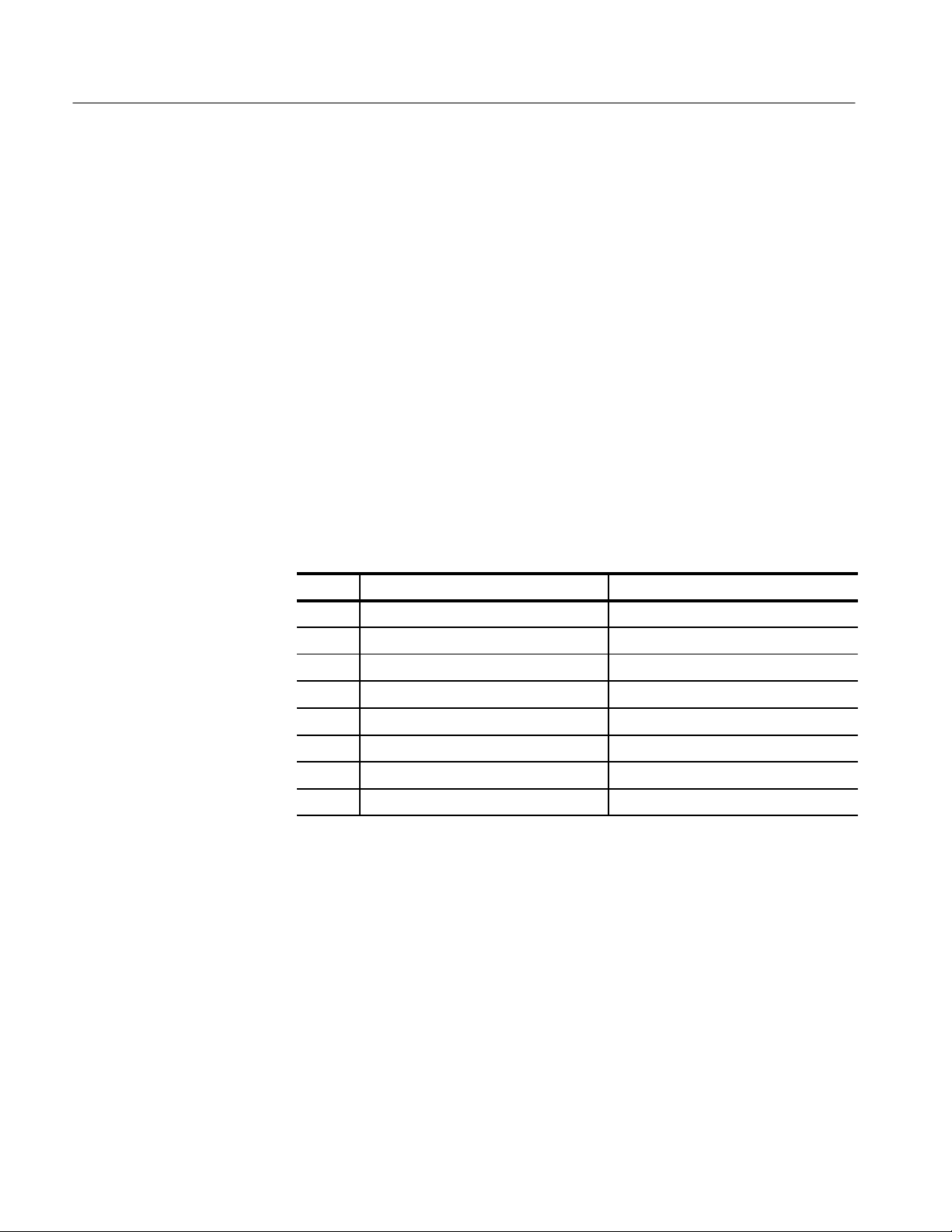
Microprocessor Chip Selects. Four programmable chip select lines are used on
the training board. Table 2–1 lists the chip select lines and how they are used.
For information on the memory mapping, refer to Memory Maps beginning on
page 2–22.
T able 2–1: Microprocessor chip select lines
Chip
select
CS0* Boot and system Flash ROM
CS1* User and system RAM
CS2* User and application ROM
CS3* Memory mapped input and output
Memory space usage
TLA QuickStart Technical Reference Manual
2–1
Hardware Features
Microprocessor Interrupts. Four external interrupts are used on the training board:
IRQ3*, IRQ5*, IRQ6*, and IRQ7*. You can assert the signals through the push
buttons on the training board or through the parallel control port.
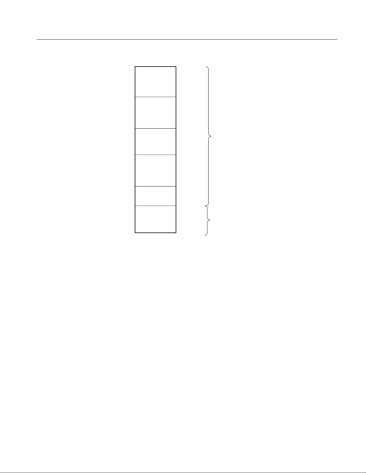
Microprocessor Parallel Input/Output Port. The microprocessor has a general
purpose parallel input/output port (PORTA) that uses the upper eight address
lines. The port is used for general purpose (application defined) input and output
bits, serial clock bits, and serial data bits. Table 2–2 shows the bits of the port
and the corresponding signals. The PORTA signals are accessible on bus
interface connector (J180).
T able 2–2: PORTA signals
Bit Signal name Function
0 SCL Serial clock bit
1 SDA Serial data bit
2 CNTLIN1 Application defined input control bit
3 CNTLIN2 Application defined input control bit
4 CNTLIN3 Application defined input control bit
5 CNTLOUT1 Application defined output control bit
6 CNTLOUT2 Application defined output control bit
7 CNTLOUT3 Application defined output control bit
Microprocessor Output Bits. The microprocessor has an output port that shares
the signal lines with the signal lines of the dedicated serial ports (A and B). Two
of the bits have specific uses. The OP4 bit generates the clears the external
trigger input. The OP6 bit generates the trigger output signal (EXTRIGOUT).
Both signals are active low signals.
Delay Line Memory. The delay line memory is a 16-bit read and write register to
demonstrate setup and hold timing violations during read operations. Data can be
written and then read from the same memory location; the data read should equal
the written data. When you program the delay line with a small delay, a setup
violation occurs during the read operation and the data read back will be different
than the written data. When you program the delay line with a large delay, a hold
violation occurs during the read operation and the returned data will be different
than the written data.
2–2
TLA QuickStart Technical Reference Manual
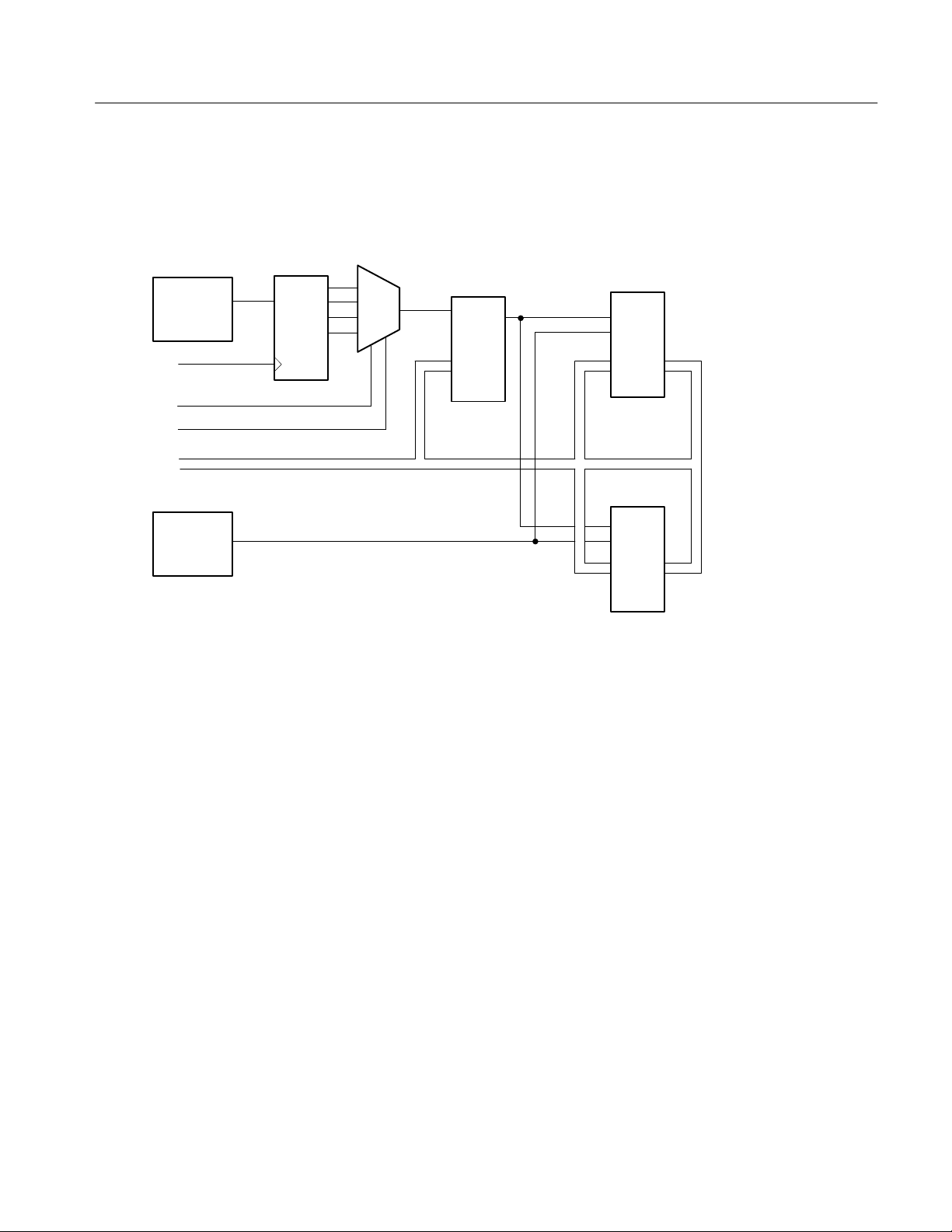
Clockout
Dlyclksel0
Dlyclksel1
Data<0..15>
Delayed
read strobe
gen logic
Figure 2–1 shows a block diagram of the programmable delayed read memory.
Read strobe delay
shift register
62 ns/Step
Shift
register
Mux
0–125 ns
programmable
delay
In
Out
Prog.
delay
line
Hardware Features
Upper byte
memory
OE
CLK
Data<8..15>
Lower byte
memory
Read/Write
logic
Figure 2–1: Programmable delayed read memory block diagram
Programmable Delay Clock Select. The programmable delay clock select consists
of a serial shift register clocked by the microprocessor system clock. The input to
the shift register is the delayed shift register read strobe which is delayed in
multiples of the clock period. The input read strobe and three output bits of the
shift register are routed to a four-bit input multiplexer. The multiplexer selects
one of the four read strobes.
Programmable Delay Line. The programmable setup and hold delay line is an
eight-bit register with 256 programmable delay settings. The delay line delays
the read strobe to the delay line memory to demonstrate setup and hold timing
violations. Each delay count increment is a 0.5 ns time delay. The minimum
delay is 00 and the maximum is FF.
OE
CLK
Data<0..7>
TLA QuickStart Technical Reference Manual
2–3

Hardware Features
Signal Sources Module
The signal sources module consists of the following groups of signals that can be
used to demonstrate logic analyzer and oscilloscope features:
Counter and pattern generator signals
Setup & Hold and trigger signals
Tapped delay line
Burst signal
Glitch signal
Metastable data and clock signals
Step signal
Runt pulse and missing pulse signal
Single-shot and narrow pulse signal
Staircase signal
Counter and Pattern Generator Signals. You can use the two 16-bit (or one 32-bit)
counter and pattern generators to demonstrate multiple logic analyzer and logic
scope capabilities. Both counter and pattern generators can be configured by
software. The counters can be programmed to count up or down. They can be
clocked by the 50 MHz oscillator or through an external trigger input.
Setup and Hold Trigger Signals. Use the setup and hold trigger signals to
demonstrate how logic analyzers can measure or trigger on setup and hold
signals. The setup and hold signals are generated by a four-bit counter. The
counter can be controlled by software to demonstrate setup violations or hold
violations.
T apped Delay Line. Use the tapped delay line as basic pattern generator to show
signal skew, timing resolution, and sampling rates.
Burst Signal. Use the burst signal to demonstrate logic analyzer transitional
timing.
Glitch Signal. Use the glitch signal to demonstrate logic analyzer and oscilloscope
triggering.
Metastable Data and Clock Signals. Use the metastable data and clock signals to
demonstrate logic analyzer and oscilloscope setup and hold triggering.
2–4
TLA QuickStart Technical Reference Manual

Hardware Features
Step Signal. Use the step signal to demonstrate analog bandwidth and triggering
of oscilloscopes and logic analyzers.
Runt Pulse and Missing Pulse Signal. Use the runt pulse and missing pulse signal
to demonstrate oscilloscope pulse triggering features. You can also use it to
demonstrate logic analyzer 4 ns counter/timers and time-qualified triggers.
Single-Shot Narrow Pulse Signal. Use the single-shot narrow pulse signal to
demonstrate analog bandwidths of oscilloscopes and logic analyzers. You can
also use this signal to demonstrate real-time sampling capabilities of the
oscilloscopes and logic analyzers.
Staircase Signal. Use the staircase signal to demonstrate the oscilloscope
acquisition modes and glitch detection.
User Interface Module
The user interface module consists of the following elements:
A two-line by 16-character LCD display
Four push-button switches
A reset switch
Two 10-segment LED indicators
LCD Display . The main display device is a two line by 16 character LCD display.
The readout is controlled by software and by the four push-button switches.
The microprocessor communicates with the display by placing the upper eight
bits on the data bus. The LCD display has a register select (RS) bit. When the
RS bit is low, it selects the instruction register; when the bit is high, it selects the
data register.
Push-button Switches. The four push-button switches connect to the four external
interrupt lines of the microcontroller. The switches select and control the
programs in the training board. The LCD readout displays the push-button
switch functions. The right-most switch halts the program and asserts a
nonmaskable interrupt (NMI) signal to IRQ7.
Reset Switch. The Reset switch is a momentary push-button switch that provides
a system reset to the microcontroller.
TLA QuickStart Technical Reference Manual
2–5

Hardware Features
LED Indicators. Two 10-segment LED indicators display bit patterns for various
software and hardware demonstrations. The first sixteen LED segments (labeled
0 through 15) represent data bits. Bits 16 and 17 represent the LAPort input and
output enable status. Bit 18 indicates whether the external trigger input is
enabled. Bit 19 shows the status of the Halt signal line.
Input and Output Connectors
The TLA 7QS Training Board has the following input and output port connectors:
Two serial ports
A logic analyzer control port
Two trigger BNC connectors
A background debug mode connector
A JTAG connector (pins not installed on board)
Power input connectors
Bus interface connector
These connectors and their pin information are described in the Theory of
Operation chapter beginning on page 4–9.
Serial Port Requirements
Serial Port B is the main serial port for connecting the training board to an
external host. It is also used to monitor programs and to download and execute
firmware. The serial port uses hardware handshaking to control communications
between the host and the training board.
In addition to the minimum RS-232 signals (RX, TX, and GND) for serial
communications, the handshaking signals (CTS and RTS) are required for
connection between a terminal (or computer) and the training board.
Serial Port B on the training board is designed as a DTE (data terminal equipment) device. Most terminals and personal computers with serial ports are also
configured as DTE devices. Therefore, the signal connections between the
terminal and Serial Port B on the training board may require an null modem
connection.
2–6
The left side of Figure 2–2 shows the standard full null modem connection. The
minimum null modem connection required for the training board is shown on the
right side of Figure 2–2.
TLA QuickStart Technical Reference Manual
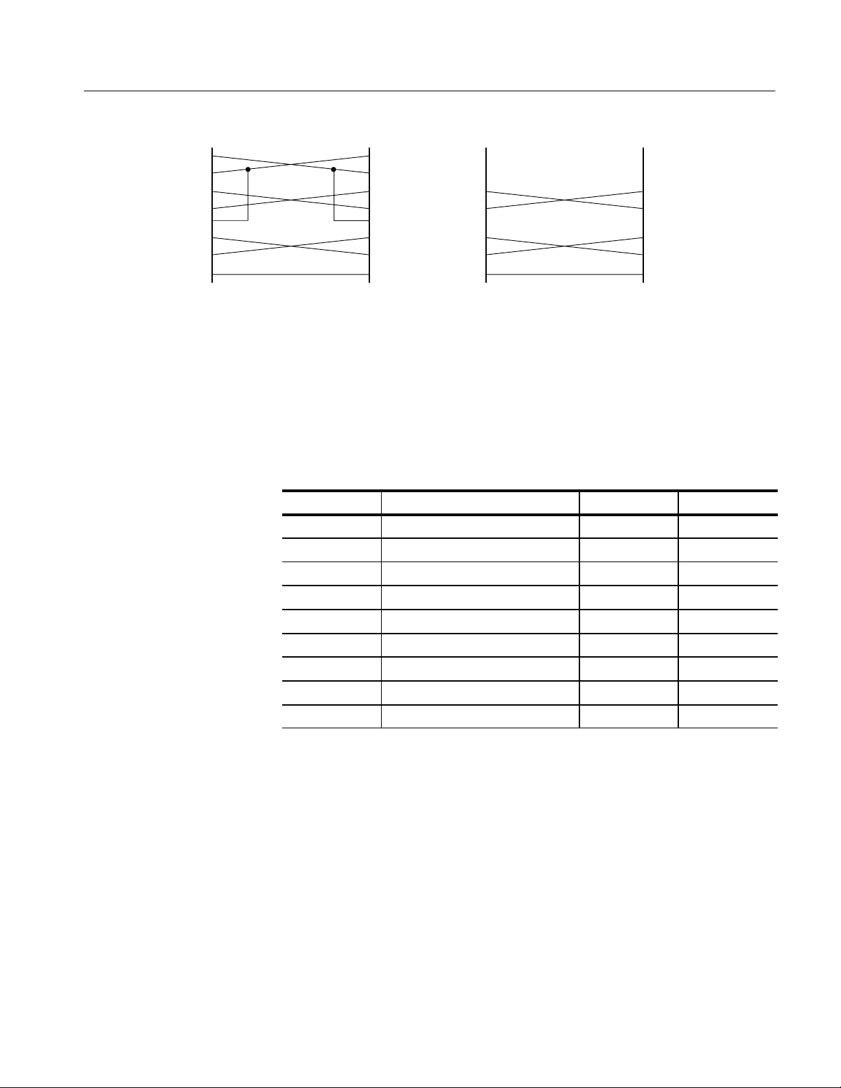
Hardware Features
DTR
DSR
RTS
CTS
DCD
TXD
RXD
GND
Standard null modem connection Minimum null modem connection
DTR
DSR
RTS
CTS
DCD
TXD
RXD
GND
DTR
DSR
RTS
CTS
DCD
TXD
RXD
GND
required for the training board
Figure 2–2: Null modem connections
Table 2–3 shows the connector pinouts for the DB9 and DB25 serial port
connectors.
T able 2–3: RS-232 connector pinouts
Signal Name DB9 pins DB25 pins
DCD Data carrier detect 1 8
RXD Receive data 2 3
DTR
DSR
RTS
CTS
DCD
TXD
RXD
GND
TXD Transmit data 3 2
DTR Data terminal ready 4 20
GND Signal ground 5 7
DSR Data set ready 6 6
RTS Request to send 7 4
CTS Clear to send 8 5
RI Ring indicator 9 22
For more information on the serial ports on the training board refer to the Serial
Ports on page 4–11.
TLA QuickStart Technical Reference Manual
2–7

Software Features
This section describes software operation, embedded programs, and diagnostics
available with the TLA 7QS Training Board.
When you first apply power to the the training board, or when you press the
Reset button, the training board initializes the 68340 registers, runs the power-on
diagnostics, and then starts the normal operation.
Operating Modes
There are three modes of normal operation for the training board:
Stand-alone mode
Host-controlled mode
Debug mode
The software routines are available in both stand-alone operation and host
controlled mode (unless specified otherwise).
Stand-Alone Mode
Host-Controlled Mode
In the stand-alone mode, operation of the training board is controlled by the
button interface. All program information is sent to the liquid crystal display
(LCD). Menu selections are displayed on the LCD as well as the current function
of the four buttons mounted directly below the display.
You can scroll through the menu selection by pressing the UP or DN (down)
buttons. Pressing the RUN button starts the selected software routine. Pressing
the STOP button halts the selected routine. The display on the LCD may change
depending on the selected software routine. Refer to LCD User Interface on page
2–15 for more detailed information on controlling the training board in the
stand-alone mode.
In the host-controlled mode, the operation of the training board is controlled
through Serial Port B. You can connect the training board to a host (such as a PC
running an RS-232 application such as HyperTerminal). The menu selections are
the same as in the stand-alone mode; however, because of the larger display,
more verbose descriptions are possible.
TLA QuickStart Technical Reference Manual
2–9

Software Features
NOTE. You may need to use a null modem to connect the training board to your
PC. For information on using a null modem, refer to Serial Port Requirements
on page 2–6.
Additional menu choices are available that are not used in the stand-alone mode.
These choices include downloading an S-record file to user flash memory and
starting the SDS (Software Development Systems) target monitor program. A
list of embedded programs and routines is described in detail under Embedded
Programs beginning on page 2–10.
While the training board is connected to host, the training board operation can
still be controlled from the buttons and data will be displayed on the LCD as
well as on the remote menu.
Debug Mode
Main Software Routine
Embedded Programs
The debug mode is intended to be used during program development. While in
the debug mode, the training board runs a target monitor (a ROM resident
program) that communicates with the SDS SingleStep development software.
The debug mode lets you develop, download, and test programs before you
commit them to flash memory. The debug mode also provides direct access to
the hardware on the training board.
The main software routine is a message processor that runs in an endless loop.
User and instrument actions, such as pressing a button, generate messages which
are posted to a message stack. The routine continuously checks the stack for
messages and sends new messages to the appropriate action routine.
Most messages are generated by an interrupt service routine. The buttons,
timers, and RS-232 circuitry have individual interrupt service routines. When an
interrupt is serviced, the interrupt service routine posts the appropriate message
to the message stack and then returns control to the processor.
2–10
This section describes the embedded programs that are available with the current
version of the training board. The programs, routines, or tests described in this
subsection are available at product introduction. Others can be added by the user
as necessary.
The programs use several subroutines to provide logic analyzers a means of
demonstrating performance analysis. All initialized variables are mapped into
SRAM so values can be changed. The variables return to the default values at
power-on or when the training board is reset.
TLA QuickStart Technical Reference Manual

Software Features
LITES
STOP LITES
STRINGS
COUNTER
The Lites program strobes the LED segments from right to left and then left to
right. The program also writes the phrase “Making It Happen” to Serial Port B.
The Stop Lites program lights specific LEDs in a predetermined sequence. The
LEDs are lighted in a sequence to emulate two traffic lights (hence the name
Stop Lites). One set of lights change from green to amber to red. After the light
is red, a second set of lights cycles from green to amber to red. The sequence
continues until interrupted by the user.
The Strings program continuously sends the string “The quick brown fox jumped
over the lazy dog” to Serial Port B.
The Counter program controls the counter-pattern generator circuitry on the
training board (J840, J940, J830, and J930). Push the RUN button to start the
program and to display the current settings. To change any of the settings, push
the F1, F2, or F3 buttons. You can change the program settings by pushing the
appropriate buttons as described below:
Push the F1 button to select the counter size, 16 bits or 32 bits.
Push the F2 button to select the counter direction, up or down.
PATTERN GEN
SHOW CYCLES
Push the F3 button to select the counter clock source, internal or external.
Push the F4 button to accept the changes.
The Pattern Gen program controls the counter-pattern generator circuitry on the
training board (J840, J940, J830, and J930). Push the RUN button to start the
program and to display the current settings. To change any of the settings, Push
the F1, F2, or F3 buttons. You can change the program settings by pushing the
appropriate buttons as described below:
Push the F1 button to select the data pattern, A5 or F0.
Push the F2 button to select the clock speed, normal, divide-by-four,
divide-by-sixteen, or SIM timer module 2.
Push the F4 button to accept the changes.
The Show Cycle program routes the M68340 internal bus cycles to the external
bus. The logic analyzer can be set up to capture and analyze these bus cycles.
TLA QuickStart Technical Reference Manual
2–11

Software Features
WAIT STATE
INT LATENCY
PGM DELAY
The Wait State program varies the M68340 wait states from zero to three on CS2
and CS3. After starting the program, push the F1 button to select the number of
wait states. You can then use a logic analyzer to capture and analyze the impact
of the wait states on system performance.
The INT Latency program generates an interrupt at random intervals of time.
This program provides a means for logic analyzers to measure the time between
an INT assertion and an INT acknowledge. The LEDs strobe across the LED
display while the program runs.
The PGM Delay program controls the Setup and Hold circuitry on the training
board (J850). You can use the buttons to select the clock speed and to specify a
delay from 00 Hex to FF Hex.
When the program runs, it sends a value of 5555 Hex to a register and is then
read back. The read select line is delayed by the programmed amount. The
resulting value is displayed by the LED bank. If the displayed value is not
5555 Hex, then you know that an error occurred.
Push the RUN button to start the program and to display the current settings. To
change any of the settings, push the F1, F2, or F3 buttons. You can change the
program settings by pushing the appropriate buttons as described below:
AUTO DELAY
PULSE
Push the F1 button to select the clock, normal, divide-by-two, divide-by-
four, or divide-by-eight.
Push the F2 button to change the most-significant byte of the delay value.
Push the F3 button to change the least-significant byte of the delay value.
Push the F4 button to accept the changes.
The Auto Delay program is similar to the PGM Delay program except that the
clock and delay times are automatically sequenced through all possible values.
The Pulse program generates a monostable pulse when you press the F1 button.
The pulse is generated by SIM timer module 1. The 1 V pulse is sent to the
PULSE pins (J971-3 and J870-5, 6) in the Analog Signals section of the training
board. A TTL-level pulse is available on the C0-4 section (T1) of the microprocessor signals section on J750-5.
2–12
TLA QuickStart Technical Reference Manual
Software Features
SETUP/HOLD
PGM FLASH
The Setup/Hold program controls the Setup and Hold circuitry on the training
board (J850). The program sends a four bit count pattern to DATA pins 0–3
(J850-1 though J850-4). The same pattern is sent to the QOUT pins 0–3 (J850-5
through J850-8). However, the count data at the QOUT pins is skewed by a
specified amount of time.
Push the RUN button to start the program and to display the current settings. To
change any of the settings, Push the F1, F2, or F3 buttons. You can change the
program settings by pushing the appropriate buttons as described below:
Push the F1 button to select the clock, normal, Setup (CLK 2), or Hold
(CLK 1).
Push the F2 button to enable (YES) or disable (NO) a toggle feature. The
feature toggles the clock between Normal and Hold or between Setup and
Hold when a count of 0A H is reached.
Push the F4 button to accept the changes.
The PGM flash program provides a means for loading user programs into the
User area of the flash ROM. You can also use the program to bulk-erase the user
flash ROM. Any new user programs will be added to the menu display and can
be selected in the same manner as any other program. To use this program, you
must be operating in the host-controlled mode. Instructions for creating a new
user program are described in Creating Programs for the Training Board
beginning on page 2–29.
LAPORT ENABLE
CAUTION. Exiting or interrupting the program prematurely can corrupt the user
flash memory. Do not execute this program if you are not operating in the
host-controlled mode.
If you start the program from the training board, you will be asked to verify your
intentions (select YES to continue, NO to exit the program). You can only exit or
interrupt the program by pushing the Reset button on the training board.
The LAPort Enable program controls the LAPort functions of the training board.
The LAPort is normally enabled during reset or when you apply power to the
training board. This program allows you to enable or disable the port.
Push the RUN button to start the program and to display the current settings. To
change any of the settings, push the F1 button. You can change the program
settings by pushing the appropriate buttons as described below:
Push the F1 button to enable or disable the port.
Push the F2 button to count up to select the port lines.
TLA QuickStart Technical Reference Manual
2–13

Software Features
Push the F3 button to count down to select the port lines.
Push the F4 button to accept the changes.
The three LAPort lines are selected by binary values from the F2 or F3 buttons.
The value written to the output is displayed on the LCD as a binary number. For
example, to set the LAPort output line 1 high and others low, select the binary
value 010.
TRIG ENABLE
DIAGS
MONITOR
The Trig Enable program enables or disables the Trigger In or Trigger Out
features on the training board. When enabled, a Trigger In signal will generate an
IRQ7 interrupt and a Trigger Out signal will generate an IRQ6 interrupt.
When disabled, the Trigger In signal functions as an external clock for the
counters. The Trigger Out circuitry functions normally but does not assert an
IRQ6 interrupt.
Push the RUN button to start the program and to display the current settings.
Push the F2 button to enable or disable the Trigger In and Trigger Out feature.
Push the F1 button to manually generate a Trigger Out pulse; the training board
responds by displaying an asterisk on the LCD.
The Diags program executes the extended diagnostics. For more information on
diagnostics, see Diagnostics on page 2–16.
The Monitor program starts the SDS Target Monitor routine in preparation for
running the SDS SingleStep debugger. This selection is only useful if you have a
copy of the SDS SingleStep program running on a host computer. You will be
prompted to verify your intention to run this program. To exit this program, push
the Reset button.
Interrupt Service Routines
Interrupts 3, 5, 6, and 7 have individual handlers. Each handler posts a global
message that will be read by the main function. Timer 1, Timer 2, and RS-232
can also generate interrupts that will have their own interrupt service routines.
2–14
TLA QuickStart Technical Reference Manual
LCD User Interface
Software Features
The LCD Interface consists of the liquid crystal display and four buttons on the
training board. The UP, DN, RUN, and STOP images on the LCD correspond to
the buttons located directly below the display.
UP and DN Buttons
RUN Button
STOP Button
RS-232 Interface
Pushing either button causes interrupts. The interrupts post messages to the main
routine. Push the UP button to scroll backward through a list of programs. Push
the DN button to scroll forward through a list of programs.
Push the RUN button to start a program. While a program runs, the UP, DN, and
RUN images on the display are replaced by the prompt “RUNNING.” Other
buttons are ignored, except when the program prompts you to push a button.
Push the STOP button to halt a program. Pushing the STOP button while no
tests are running has no effect.
The RS-232 interface provides a means of controlling the training board from a
host. The host connects to the training board through RS-232 Serial Port B. The
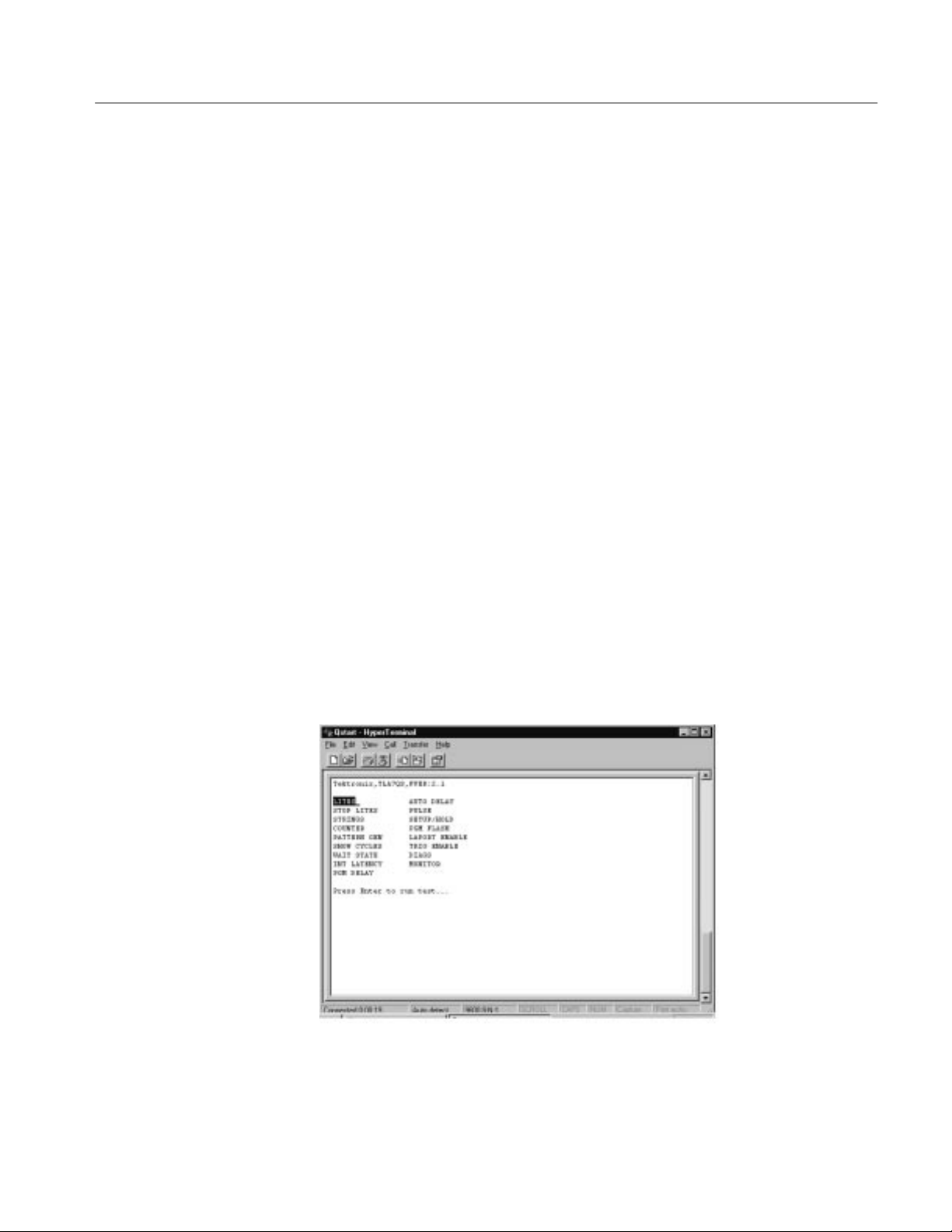
interface displays a menu (see Figure 2–3) containing all of the tests programmed in the training board.
Figure 2–3: Remote menu
TLA QuickStart Technical Reference Manual
2–15

Software Features
Diagnostics
The interface runs at a baud rate of 9600 with hardware flow control. You should
use a terminal emulation program on a PC such as HyperTerminal.
The ANSI escape codes provide cursor control. Press an arrow key on the
terminal keyboard to move between highlight selections in the menu. If the
terminal does not have any arrow keys, press the J or K keys to change selections.
Press the Enter or Return key to start a program or test. The terminal displays the
following message:
Press any key to stop a test. The terminal returns control to the menu selections.
The diagnostics test the basic operation of the training board. The power-up
diagnostics run when power is applied to the training board or when the RESET
is asserted. Some of the extended diagnostics require human interaction.
LCD Test
Serial Port Tests
To start the extended diagnostics, select DIAGS on the display. Push the run
button to start the extended diagnostics. The diagnostics run automatically and
only require user interaction when connecting the RS-232 cables. The extended
diagnostics test the following areas of the training board:
LCD
Serial ports
ROM
RAM
Upon completing the diagnostics, the test results are temporarily listed on the
display.
The LCD is tested by displaying a pattern that illuminates all bits on the display.
Visually verify that all bits are illuminated.
The serial port test consists of two kinds of tests. The first test is an internal
loopback test. The test places the serial ports into the loopback mode. A
character is transmitted to the port, received, and compared. The test passes
when the received character matches the transmitted character.
2–16
TLA QuickStart Technical Reference Manual

Software Features
The second test requires connecting a terminal to Serial Port A (9-pin subminiture D connector). The test pauses until you connect the cable and then push the
Run button to continue. The test string, “Testing serial port A,” is transmitted
through the port. The test passes when when you see the test string is on the
terminal screen.
The test is repeated for Serial Port B using a two by five shrouded square-pin
connector (see Table 4–8 on page 4–11 for pinout information).
ROM Test
RAM Test
The ROM test checks the read-only memory. The ROM is checked by reading a
specific location for a confidence word. If the returned value matches the
confidence word, the ROM is assumed to be good. A Pass/Fail condition is
displayed on the LCD at the completion of the tests.
The RAM is tested by writing a value and then reading the value. If the returned
value matches the written value, the test passes. A Pass/Fail condition is
displayed on the LCD at the completion of the tests.
TLA QuickStart Technical Reference Manual
2–17

Memory Maps
This section provides information on the memory maps for the TLA 7QS
Training board. The first part of this section provides information on the memory
mapped input and output. The rest of this section lists the actual memory maps.
Memory Mapped Input and Output
The training board has 2 Mbytes of memory mapped input and output. The
memory is divided into eight equal segments. Table 2–4 lists the names and
addresses of the memory mapped input and output devices.
T able 2–4: Input and output device addresses
Device Address Input/output type Memory depth and width
LCD display $40 0000 Read/write 1 X 8
LED display $44 0000 Write only 1 X 16
Input control bits $48 0000 Read only 1 X 8
Output control bits $4C 0000 Write only 1 X 16
Setup and hold delay line $50 0000 Write only 1 X 8
Setup and hold memory $54 0000 Read/write 1 X 16
Low counter /pattern generator $58 0000 Write only 1 X 16
High counter/pattern generator $5C 0000 Write only 1 X 16
LCD Display
LED Displays
TLA QuickStart Technical Reference Manual
The liquid crystal display has two eight-bit registers selected by the register
select (RS) bit. When the RS bit is low, it selects the instruction register, when it
is high it selects the data register.
The training board has two 10-segment LED displays. The segments are used as
follows:
The first 16 segments connect directly to the 16-bit data lines and are used
for general purpose applications. Bit 0 is the right-most segment on DS880.
Bit 16 represents the LAPort input enable status. The input circuit uses a
flip-flop to clock in data by an external computer. The enable control bit
connects to the output enable of the flip-flop. When the LED is on (low
signal) the input is enabled and input signals are connected to the training
board.
2–19
Memory Maps
Bit 17 represents the LAPort output enable status. The output circuit uses a
transparent latch. When the LED is on (low signal), the output is enabled and
signal changes on the training board are sent to the output port. When the
LED is off, the output data is latched to last transmitted value (unknown at
power-on). The bit is inverted for proper polarity to the latch.
Bit 18 represents the external trigger input and output interrupt enable status.
When the LED is on, an external input or output trigger causes interrupts
IRQ7 and IRQ6 respectively.
The last bit represents the status of the Halt* signal. When the LED is on,
the Halt* line is asserted.
Input Control Bits
Register
The input control bits register is a general purpose register that monitors signals.
Table 2–5 lists the input control bits and the associated signals. The signals are
intended for diagnostic read-back purposes. See Figure 2–7 on 2–26 page for
memory mapping information.
T able 2–5: Input control bits
Bit Signal name Function
0 LAPORTIN* Control bit readback
1 LAPORTOUT* Control bit readback
2 TRIGGERIN Control bit readback
3 CNTRDIAG Control bit readback from Mux
4 SIGCLK1 Microprocessor timer 1 readback
5 SIGCLK2 Microprocessor timer 1 readback
6 SCL Serial clock (PortA bit 0) readback
7 SDA Serial clock (PortA bit 1) readback
2–20
TLA QuickStart Technical Reference Manual

Memory Maps
Output Control Bits
Register
The output control bits register is a 16-bit input register used to assert signals.
Table 2–6 lists the output control bits and the associated signals. See Figure 2–7
on 2–26 page for memory mapping information.
T able 2–6: Output control bits
Bit Signal name Function
0 LCDRS LCD register select
1 DL YCLKSEL0 Delay generator clock select Mux bit 0
2 DL YCLKSEL1 Delay generator clock select Mux bit 1
3 LAPORTIN* LAPort input enable
4 LAPORTOUT* LAPort output enable
5 TRIGGERIN* External trigger input enable
6 EXTCLKEN External counter clock enable
7 CNTR16BIT* 16-bit or 32-bit counter select
8 PATCLKSEL0 Pattern generator clock selector Mux
bit 0
9 PATCLKSEL1 Pattern generator clock selector Mux
bit 1
Programmable Delay
Setup and Hold Violation
Circuit
Read-Write Setup and
Hold Violation Memory
10 LOCNTREN* Low counter count enable
11 LOCNTRSEL* Low counter or pattern select
12 LOCNTRUP* Low counter count up/down select
13 HICNTREN* High counter count enable
14 HICNTRSEL* High counter or pattern select
15 HICNTRUP* High counter count up/down select
The programmable setup and hold delay line is an eight-bit register with 256
programmable delay settings. The delay line delays the read strobe to the delay
line memory to demonstrate setup and hold timing violations. Each delay count
increment is a 0.5 ns time delay. The minimum delay is 00 and the maximum
is FF.
The delay line memory is a 16-bit read and write register to demonstrate setup
and hold timing violations during read operations. Data can be written and then
read from the same memory location; the data read should equal the written data.
When you program the delay line with a small delay, a setup violation occurs
during the read operation and the data read back will be different than the written
data. When you program the delay line with a large delay, a hold violation occurs
during the read operation and the data will be different than the written data.
TLA QuickStart Technical Reference Manual
2–21

Memory Maps
Low Counter Pattern
Generator Data
High Counter Pattern
Generator Data
Memory Maps
The low counter pattern generator data register is a 16-bit write-only register that
stores a data value in the low counter pattern generator.
The high counter pattern generator data register is a 16-bit write-only register
that stores a data value in the high counter pattern generator.
Figures 2–4 through 2–8 show the following memory maps for the TLA 7QS
Training board:
A full memory map
System and user static RAM
User EEPROM and flash
Input and output
System EEPROM and flash
2–22
TLA QuickStart Technical Reference Manual
Memory Maps
CS1
CS2
CS3
CS0
2 MB
User/System
SRAM
Space
2 MB
User
EEPROM/Flash
Space
2 MB
Input/Output
Space
2 MB
System
EEPROM/Flash
Space
8 MB
UNUSED
4 GB
Available on
Extender Bus
00 0000
$20 0000
$40 0000
$60 0000
$80 0000
$FF FFFF
$FFFF FFFF
On Board Memory Space
16 MB Address Space
24 Address Lines (A0—A23)
Extended Memory Space
4 GB Address Space
Available on Extender Bus using the upper
eight Address Lines (A24—A31)
Figure 2–4: Full Memory Map
TLA QuickStart Technical Reference Manual
2–23

Memory Maps
256K
256K
512K
512K
512K
128 K X 16 K
SRAM
128 K X 16 K
SRAM
Unused
Unused
Unused
$00 0000
$04 0000
$08 0000
$10 0000
$18 0000
1K
15K
16K
32K
196K
496K
Exception
Vectors
Monitor
Supervisor
Space
Supervisor
Stack Pointer
Space
User
Stack Pointer
Space
User
Program
Space
User
Program
Space
$00 0000
$00 03FF
$00 3FFF
$00 7FFF
$01 0000
$04 0000
$07 FFFF
$1F FFFF
Figure 2–5: System and user static RAM
2–24
TLA QuickStart Technical Reference Manual

$20 0000
Memory Maps
512K
512K
512K
512K
256K X 16
EEPROM/Flash
$28 0000
Unused
$30 0000
Unused
$38 0000
Unused
$3F FFFF
Figure 2–6: User EEPROM and Flash
TLA QuickStart Technical Reference Manual
2–25

Memory Maps
256K
256K
Input Control Bits
256K
Output Control Bits
256K
Programmable
256K
Delay Line Memory
256K
Pattern Generator
256K
Pattern Generator
256K
LCD Display
Output
Read/Write
LED Display
Output
Write Only
Read Only
Write Only
Delay Line
Write Only
Read/Write
Data
Write Only
Control
Write Only
$40 0000
$44 0000
$48 0000
$4C 0000
$50 0000
$54 0000
$58 0000
$5C 0000
$5F FFFF
Figure 2–7: Input and output
2–26
TLA QuickStart Technical Reference Manual
$60 0000
Memory Maps
512K
512K
512K
512K
256K X 16
EEPROM/Flash
$68 0000
Unused
$70 0000
Unused
$78 0000
Unused
$7F FFFF
Figure 2–8: System EEPROM and Flash
TLA QuickStart Technical Reference Manual
2–27

Creating Programs for the Training Board
This section provides information on creating programs for use with the training
board. Information is provided under the following subsections:
Preparation
Writing the program
Compiling and linking code
Writing an image to the flash memory
Rebooting and running the program
Preparation
To create programs for the training board you will need the SDS CrossCode
C 68K software package from Software Development Systems (the C++ option
is not required) and some software tools from Tektronix. You will use these
packages to write the code and to download the programs to the training board.
Software Development
Systems Tools
Tektronix Software Tools
The SDS CrossCode C/C++ 68K package includes the C compiler, assembler,
linker, and other utilities necessary to convert your source code into 68K code.
Although not required, the SDS SingleStep debugger package may also prove to
be helpful.
The software packages come in several versions which vary mainly in the
connections to the target. The OnChip debugger connects to the background
Debug Mode (BDM) port on the training board through a cable adapter from the
PC printer port. The Target Monitor version connects through a standard serial
COM port to the SDS monitor program which is resident on the training board.
The Target Monitor version is easier to connect, but it is also slower than the
BDM version. The BDM version was used to develop the training board.
In addition to the software packages from Software Development Systems, you
will also need the object file (mongoose.obj) and the linker specification file
(combine.spc). If you intend to reuse some of the code already present on the
training board (such as the code to display strings on the LCD), you will also
need the include files for the training board.
Appendix A: Source Code contains examples of the combine.spc file and a list of
the Tektronix supplied software available with this technical reference manual.
TLA QuickStart Technical Reference Manual
2–29

Creating Programs for the Training Board
Writing the Program
The following procedures provide information on writing the program code for
the training board. You may want to refer to Appendix A: Source Code for a
sample program. The procedures consist of the following steps:
Create the menu entry
Include the user header file
Create a dummy function
Write the code
Create the Menu Entry
Include the User Header
File
The menu for the training board is a linked list structure. The menu structure is
defined in the include file, menu.h. The file is type defined as MENU. You need
to define the following information in the structure:
The menu text to be displayed
The row location of the remote menu text
The column location of the remoter menu text
A pointer to the function to be executed
The following example shows how a sample menu entry with all of the
definitions provided.
MENU myItem = {
My Text", /*text that will be displayed on the menu */
3, /*row location of the remote menu item */
35, /*column location of the remote menu item */
mytestfunction /*pointer to the function to be executed */
};
You must include the user header file, user.h. This file declares a constant that is
located in a specific place in the user memory on the training board. The constant
is checked every time the training board is reset. If the header file finds the
constant, the software will look for menu entries to be added to the menu list.
Create a Dummy Function
2–30
You must include a dummy function to create the proper code and C frame. Do
not include any code in the function, the function must remain empty. The
dummy function is required to allow your code to be appended to the software
on the training board.
TLA QuickStart Technical Reference Manual

Creating Programs for the Training Board
Write the Code
Write your code using normal C or assembly language. You can use any of the
functions for the training board, or create your own functions. Refer to Appen-
dix A: Source Code for a sample program. You may also want to refer to the code
supplied on the floppy disk accompanying this manual.
Compiling and Linking Code
The following procedure shows how to compile and link the code using the
CrossCode 68K application.
Compile the Code
Link the Code
Compile the code using commands and flags as shown below:
Although you may want to use other combinations of compiler flags, not all
combinations have been tested. However, the flags used in the above example
should work for your application.
After compiling the code, you must link the code. To link the code into an object
file, you will need the following items:
An object file (the output file from the compile operation)
The firmware object file (mongoose.obj)
A linker specification file (combine.spc)
The firmware object file is necessary because a successful link requires the
symbol table from the TLA 7QS software that is programmed in the system flash
ROM. For the symbol table to be valid, the firmware object file must be the
same revision as the firmware on the training board.
The linker specification file tells the linker file where to locate some specific
regions, such as your code, data, and constants. For more information about the
linker, regions, and partitions, refer to the SDS documentation on the linker
program.
Refer to Appendix A: Source Code for examples of the C program that will add a
menu item to the main menu on the training board. The program will display the
string “Time to Switch” on the display. The appendix also includes the linker
specification file and a batch file to compile, link, and convert the output to a
Motorola S-record file.
TLA QuickStart Technical Reference Manual
2–31

Creating Programs for the Training Board
Writing an Image to the Flash Memory
Prepare to download the code into flash memory on the training board using a
downloader utility. The downloader utility will extract code bytes and convert
them into a Motorola S-record file. Make sure that you use the proper flags to
avoid ending up with an extremely large file.
Connect the training board to a PC running a terminal program such as HyperTerminal. Open up a session with the baud rate set to 9600 and with hardware
control flow. If you are unsure of the HyperTerminal settings, check the
configuration settings on the Property sheet under the File menu.
Complete the following steps to load the program in the flash memory:
1. Power on the training board and select PGM FLASH.
2. Start the PGM FLASH program and select YES when you are asked to
confirm your actions.
3. Select PGM from the menu to prepare to download the program.
Running the Program
4. When you see the prompt “Start file transfer now,” start the file transfer by
selecting Send Text File from the Transfer menu.
5. Enter the file name of the file created by the downloader program.
6. When the file transfer is complete, you will see the message “Verification is
Complete.”
After you have written the program to the flash memory, you must reset the
training board to activate the new menu. The new menu items should be
displayed after the SDS Monitor menu entry. You can now select and run the
new program using the buttons on the training board or by the cursor movement
keys on the remote menu.
2–32
TLA QuickStart Technical Reference Manual

Specifications
This chapter contains the specifications for the TLA 7QS Training Board. Within
each section, the specifications are arranged in functional groups such as:
Microprocessor System Characteristics, Signal Source Characteristics,
Hardware Characteristics, Power distribution, Mechanical Characteristics, and
Environmental Characteristics.
All specifications are warranted unless they are designated typical. Typical
characteristics describe typical or average performance and provide useful
reference information.
T able 3–1: Microprocessor signal characteristics
Characteristic Description
Microprocessor
Microprocessor component Motorola M68340
Microprocessor clock rate 16 MHz
System integration module Provides the external bus interface for the CPU32 and the DMA. Provides program-
mable circuits to perform address decoding and chip selects, wait-state insertion,
interrupt handling, clock generation, bus arbitration, watchdog timing, discrete I/O and
power-on reset timing.
DMA controller module The DMA module consists of two independent programmable channels. Each channel
has separate request, acknowledge, and done signals. Each channel can operate in a
single-address or in a dual-address mode.
Serial module The serial module contains a two-channel USART, an on-chip baud rate generator,
and is functionally equivalent to the MC68681/MC2681 DUART.
Timer module The timer module consists of two general purpose counter/timers. Each timer consists
of a 16-bit countdown counter with an 8-bit countdown prescaler.
Parallel input/output The parallel port is part of the integrated external bus interface. It can function as a
bidirectional parallel port or as address lines A24 through A31.
Background debug mode
Description The background debug mode (BDM) is a special operating mode available in the
CPU32 where normal instruction execution is suspended while special on-chip
microcode performs the functions of a debugger.
Interface The interface connector is a two-by-five shrouded square-pin header. Signals are
assigned to the pins using the standard Motorola and P&E Engineering format.
System memory
SRAM memory 128 K by 16 (512 K total)
Flash ROM memory two banks of 128 K by 16 (256 K total)
Serial EEPROM NVRAM Serial 2 K by 8
TLA QuickStart Technical Reference Manual
3–1

Specifications
T able 3–1: Microprocessor signal characteristics (Cont.)
Characteristic Description
System reset signal The reset signal is integrated into the M68340 microprocessor and connected to the
external button to reset the system.
External interrupt requests IRQ3, IRQ4, IRQ6, IRQ7
Memory-mapped functions
Chip select decoder One of eight chip select decoders to select memory-mapped functions
Input control bits register An eight-bit register to read input bits for monitoring system status and diagnostic
feedback
Output control bits register A 16-bit register to write output bits to control circuit functions and to the LAPort output
control bits
Liquid crystal display A two line by 16 character LCD readout used for system status and for application
program status
Ten-segment bar LED display Two 10-segment multicolor LED bar displays. LEDs labeled 0 through 15 represent
data bits and are used for application program output indicators. Three bits monitor
system status. The last bit indicates the status of the microprocessor HALT* line.
Memory read violation module
Memory read violation data register One 16-bit register
Read strobe coarse delay (typical) A four–to–one mulitplexer used to select one of four read strobes that are delayed by
clocked processor cycles
Read strobe fine delay (typical) 256 steps from 10 ns to 137.5 ns
Delay line resolution (typical) 0.5 ns
Logic analyzer probe connections
LASI-3 format processor probe
connections
LASI-4 format processor probe
connections
96 channels and six clocks with LASI-3 signal format
96 channels and six clocks with LASI-4 signal format
3–2
TLA QuickStart Technical Reference Manual

T able 3–2: Signal source characteristics
Characteristic Description
Counter/Pattern generator signals
Number of counter bits One 32-bit counter or two 16-bit counters
Counter clock frequency (typical) 50 MHz
Number of pattern generator bits 32
Pattern generator toggle bits Eight four-bit patterns
Pattern generator toggle frequency
(typical)
Counter/Pattern generator output
amplitude (typical)
Setup and hold counter signals
Counter data bits 4
Latched data bits 4
Normal setup and hold time (typical) > –2 ns setup time
Violation setup time (typical) < –2 ns setup time
Violation hold time (typical) > 2 ns hold time
Violation rate (typical) 625 KHz
Clock frequency (typical) 10 MHz
Signal amplitude (typical) 3.1 V to 5.1 V maximum
Tapped Delay Signals
Output bits 8
Delay time (typical) 4 ns
Output amplitude (typical) 3.1 V to 5.1 V maximum
Counter clock frequency (typical) 10 MHz
Fast edge signal
Amplitude (typical) 0.5 V high, 0 V low
Rise time (typical) < 2.0 ns
Frequency (typical) 1.5 KHz to 3.5 KHz
Narrow pulse signal
Amplitude (typical) 0.5 V to 1.0 V maximum
Pulse-width (typical) 1.0 ns to 4.0 ns
Runt pulse and missing pulse signal
Normal pulse amplitude (typical) 3.5 V to 5.5 V
Normal pulse frequency (typical) 8 MHz to 12 MHz
Runt pulse amplitude (typical) 2.0 V to 3.0 V
50 MHz, 10 MHz, 1.25 MHz, and programmable
3.5 V to 5.1 V maximum
0 V to 0.2 V minimum
0 V to 0.2 V minimum
0 V to 0.2 V minimum
Specifications
TLA QuickStart Technical Reference Manual
3–3

Specifications
T able 3–2: Signal source characteristics (Cont.)
Characteristic Description
Runt pulse frequency (typical) 1.6 Hz to 2.5 Hz
Missing pulse frequency (typical) 1.6 Hz to 2.5 Hz
Staircase signals source
Step intervals (typical) 0.5 ms per step
Staircase interval (typical) 8.0 ms per staircase
Amplitude (typical) 900 mV
Metastable glitch signal
Clock frequency (typical) 36 MHz to 44 MHz
Data frequency (typical) 8 MHz to 12 MHz
Glitch amplitude (typical) ±2 V minimum for largest glitches
Burst pulse signal
Data amplitude (typical) 3.5 V to 5.1 V
Low frequency burst pulse modulation
rate (typical)
Mid frequency burst pulse modulation rate
(typical)
High frequency burst pulse modulation
rate (typical)
Signal sources probe connections
Counter and pattern generator
connections
Setup and hold counter connections 2 by 8 square pin header and oscilloscope probe header
Digital signal connections 2 by 8 square pin header and oscilloscope probe header
Analog signal connections 2 by 8 square pin header and oscilloscope probe header
p-p
Single pulse at 763 Hz ± 75 Hz
Four pulses at 3.13 MHz ± 310 KHz
Eight pulses at 50 MHz ± 5 MHz
2 by 16 square pin headers
T able 3–3: Hardware characteristics
Characteristic Description
User interface
Halt indicator LED One LED connected to the microprocessor halt line. The LED is on when the halt line
is enabled (the microprocessor is in the halted state)
Trigger input enable LED One LED connected to the external trigger enable control bit. The LED is on when
external triggers are enabled.
LAPort output enable LED One LED connected to the LAPort output control bit. The LED is on when the LAPort
output is enabled.
3–4
TLA QuickStart Technical Reference Manual
T able 3–3: Hardware characteristics (Cont.)
Characteristic Description
LAPort input enable LED One LED connected to the LAPort input control bit. The LED is on when the LAPort
input is enabled.
Memory mapped LEDs 16 memory mapped LEDs
Liquid crystal display Two line by 16 character LCD memory mapped display
External interrupt request switches Four interrupt request signal switches for microprocessor signals IRQ3, IRQ4, IRQ6,
and IRQ7. The switches control the system software.
Reset switch One microprocessor system reset switch
Power on/off switch Applies power to the circuit board
Power indicator LED Power-on indicator LED
Signal input and output ports
Main serial port (Port B) One DB-9 connector
Auxiliary serial port (Port A) Two by five square-pin shrouded header
LAPort parallel control port DB-25 connector
Logic analyzer trigger output BNC connector
Logic analyzer trigger intput
Background debug port connector T wo by five square-pin shrouded header
JTAG Port One by six square-pin connector (square pins not installed)
1
The logic analyzer trigger input BNC connector can also be used as the external clock input connector with for clock
frequencies up to 50 MHz.
1
BNC connector
Specifications
T able 3–4: Power distribution characteristics
Characteristic Description
Low voltage power supply
Power supply input voltage (typical) +8.0 V to +15.0 V
Power supply input voltage connector 2 mm male connector with 3 A 24 V rating
Power supply output voltage (typical) +4.8 V to +5.2 V
Power supply output current (typical) 1.0 A maximum
Input power supplies
North American 120 VAC, 60 Hz input; +13.5 V, 1.5 A output
European 220 VAC, 50 Hz input; +13.5 V, 1.3 A output
United Kingdom 240 VAC, 50 Hz input; +12.0 V, 1.5 A output
Japan 100 VAC, 50 Hz to 60 Hz input; +12.0 V, 1.5 A output
TLA QuickStart Technical Reference Manual
3–5
Specifications
T able 3–5: Mechanical characteristics
Characteristic Description
Construction material
Circuit board Glass laminate
Physical Dimensions
Height 1.0 in (2.54 cm)
Length 8.1 in (20.57 cm)
Width 5.3 in (13.46 cm)
Package Dimensions
Height 3 in (7.62 cm)
Length 12.9 in (32.77 cm)
Width 11.4 in (28.96 cm)
Shipping weight 4.5 lbs (2.03 kg)
3–6
TLA QuickStart Technical Reference Manual

Theory of Operation
This chapter provides the theory of operation of the TLA 7QS training board. It
provides information on the built-in circuit modules and on the connectors on the
training board.
Circuit Board Modules
The following circuit board modules are discussed in this section:
Microprocessor module
Signal Sources module
User interface module
Input/output module
Power supply module
Microprocessor Module
The microprocessor module (schematic sheets 2, 3, 4, 5, 6, 7, and 10) consists of
a Motorola M68340 microcontroller in a TQFP package, the associated static
memory, programmable memory, nonvolatile EEPROM memory, and a
read/write register.
Static Memory. The static memory consists of two banks of 128 K by 16 (memory
implemented) using two 128 K by eight memory components. The standard
training board is loaded with only one bank of static RAM for a total of
256 K bytes.
Programmable Memory. The programmable memory (PROM) is designed to be
either EEPROM or flash memory. The PROM consists of system PROM and
user PROM. Each bank can be implemented with two 128 K by eight parts, two
256 K by eight parts, or two 512 K by eight parts.
The standard training board has both banks or PROM loaded with 128 K flash
memory for a total of 256 Kbytes of system flash and 256 Kbytes of user flash.
The system flash contains the monitor program, board utilities, and a basic set of
application programs.
The system flash is programmed at the factory and can be upgraded through field
service upgrade kits. The user flash is provided for additional applications and is
intended to be modified or added to the product by users with the proper
software development tools.
TLA QuickStart Technical Reference Manual
4–1
Theory of Operation
EEPROM Memory . The EEPROM memory is implemented with a serial 2 K by
eight serial EEPROM. The EEPROM memory is intended to be used by user
applications to store miscellaneous data such as adjustment settings and bit
patterns for the pattern generators. The EEPROM uses the I2C two-wire serial
port for reading and writing data. The two-wire port consists of a clock and a
data line. The clock and data lines are connected to two of the microcontroller
input and output Port A bits. Software routines must be written by the user to
properly read and write serial data from the EEPROM in the correct format.
Read/Write Register . A one by 16 bit read/write register implemented with
D-flip-flops is used to create memory read errors. The read errors can be
demonstrated by writing data to the register and reading the data back. The read
strobe is set to provide timing for a proper read operation or to cause a read error.
The read strobe control consists of a coarse adjustment and a fine adjustment.
The coarse adjustment delays the strobe in increments of processor clock cycles
(62.5 ns) using a clock shift register and a multiplexer to select a specific output.
The fine strobe control adjusts the time delay in 256 increments of 0.5 ns steps
for a total range of 127 ns. The time adjustment is fine enough so that it can be
calibrated to be just on the threshold of creating a read error.
Signal Sources Module
You can use the high resolution (MagniVu) mode of the TLA 700 Series Logic
Analyzers to demonstrate and measure small changes in delay adjustments.
The signal sources module (schematic sheets 21, 22, 23,and 24) consists of
several groups of signals that can be used to demonstrate logic analyzer and
oscilloscope features.
Counter and Pattern Generator Signals. Two 16-bit counter and pattern generators
can be individually programmed to operate as counters, pattern generators, or
combined as a single 32-bit counter. The counters can be programmed to count
up or down. The counter-pattern generator is controlled by the output control bits
port of the microprocessor. Table 4–1 shows the output control bits.
T able 4–1: Output control bits
Bit Signal name Function
0 LCDRS LCD register select
1 DL YCLKSEL0 Delay generator clock select Mux bit 0
2 DL YCLKSEL1 Delay generator clock select Mux bit 1
3 LAPORTIN* LAPort input enable
4–2
4 LAPORTOUT* LAPort output enable
5 TRIGGERIN* External trigger input enable
TLA QuickStart Technical Reference Manual

Theory of Operation
T able 4–1: Output control bits (Cont.)
Bit FunctionSignal name
6 EXTCLKEN External counter clock enable
7 CNTR16BIT* 16-bit or 32-bit counter select
8 PATCLKSEL0 Pattern generator clock selector Mux
bit 0
9 PATCLKSEL1 Pattern generator clock selector Mux
bit 1
10 LOCNTREN* Low counter count enable
11 LOCNTRSEL* Low counter or pattern select
12 LOCNTRUP* Low counter count up/down select
13 HICNTREN* High counter count enable
14 HICNTRSEL* High counter or pattern select
15 HICNTRUP* High counter count up/down select
The output control bits port is a 16-bit input register used to assert signals. The
bit designations and signal names are listed in Table 4–1.
The two 16-bit counter-pattern generators operate the same. They can be
configured individually as counters or pattern generators using the LOCNTRSEL* and HICNTRSEL* bits. The count up and count down bits (LOCNTRUP*
and HICNTRUP*) control the count direction. The counters can be started or
stopped with the count enable control bits LOCNTREN* and HICNTREN*.
When the counter-pattern generators function as pattern generators with the
LOCNTRSEL* and HICNTRSEL* bits, you must select a pattern clock. The
pattern clock toggles the low and high nibble of each patten bytes. The clock
selection uses a four-to-one multiplexer which is controlled using pattern clock
select bits PATCLKSEL0 and PATCLKSEL1. Table 4–2 shows the clock select
truth table. Normal pattern generator operation includes disabling the counting so
that the pattern at the output is the pattern that was loaded.
TLA QuickStart Technical Reference Manual
4–3
Theory of Operation
T able 4–2: Pattern generator clock select truth table
PATCLKSEL0 PATCLKSEL1 Clock select
0 0 Sigclk2; Microprocessor timer2 used as clock
0 1 TSTHD<3>; Setup and hold counter output
bit 3
1 0 TSTHD<1>; Setup and hold counter output
bit 1
1 1 CNTRCLK; Counter-pattern generator master
clock
The Sigclk2 clock is the microprocessor timer2 output which can be programmed to any frequency and duty cycle. It can also be programmed to stay
high or low, thus selecting the direct or alternate nibble of each byte. With the
Sigclk2 signal set low, the direct nibble is selected; the signal is high, the
alternate nibble is selected as shown in Table 4–3.
T able 4–3: Sigclk2 selections
Bit Value Counter byte output nibble
0 Direct nibble; counter bits 0–3 go to output bits 0–3
1 Alternate nibble; counter bits 0–3 go to output bits 4–7
When the counters are used as pattern generators, the patterns can be loaded by
writing the 16-bit counter value to the appropriate address. The individual
counter load strobe is enabled with a write to the high counter-pattern generator
or to the low counter-pattern generator. Table 4–4 shows the counter addresses.
T able 4–4: Counter-pattern generator addresses
Memory mapped
device
Low Cntr/Pat Gen $58 000 Write only 1 X 16
High Cntr/Pat Gen $5C 000 Write only 1 X 16
Device
address
Input/output
type
Memory depth
and width
The 50 MHz oscillator is the master clock for the counter-pattern generators. An
external clock can be used to clock the counters. The external signal is a standard
TTL level signal into the Trigger-In BNC connector. The counter clock is
selected with the memory mapped external clock control bit EXTCLKEN (bit 6
of the 16-bit output control register at address 0X4C 0000.
4–4
TLA QuickStart Technical Reference Manual

Theory of Operation
Setup and Hold Trigger Signals. The setup and hold signals (schematic 25) are
generated by a four-bit counter clocked at a 50 MHz rate. The four bits of the
counter connect to four signal ground square pin pairs so they can be measured
by a logic analyzer or by an oscilloscope. The counter output bits are routed to a
latch which is clocked by a modified version of the 50 MHz clock counter clock.
The counter clock is delayed to create a setup violation or a hold violation. The
four output bits of the latch connect to four signal-ground square pin pairs. The
delayed clock signal also connects to a signal-ground square pin pair.
Figure 4–1 shows the block diagram of the setup and hold violation counter. You
may want to refer to this block diagram as you read the following paragraphs.
4–Bit
Counter
Mux
8-Bit
50 MHz
Oscillator
Locntrsel
Patclksel0
Patclksel1
tapped
delay
line
Setup/Hold control
Clock control
Clock control
Mux
Decode
logic
Figure 4–1: Setup and hold violation counter block diagram
4-Bin
Latch
Cntr0
Cntr1
Cntr2
Cntr3
Data0
Data1
Data2
Data3
Clock
The counter clock signal is delayed by an eight-bit tapped delay line. The clock
signal is derived from one of the middle taps so it is delayed approximately 12 ns. The signal is routed through a multiplexer for time delay matching
purposes. All four inputs of the multiplexer have the same clock signal so that
the clock input to the counter always has a steady clock signal.
The delayed counter clock is selected by the setup and hold clock multiplexer
(Mux). Three clock signals go to the four inputs of the Mux. A nominal delay
clock goes to two inputs of the Mux. A setup delay clock with less delay than the
counter clock and a hold delay with more delay than the counter clock are the
other two inputs to the Mux.
TLA QuickStart Technical Reference Manual
4–5
Theory of Operation
The setup and hold violation counter operates in the following manner. The
four-bit counter has a continuous count at 50 MHz. The four output bits and the
clock can be measured. However, the clock is skewed in time at a specific
counter output bit pattern of 1010. The time skew can be in either direction,
positive or negative, compared to the counter clock. The time skew can be
measured and analyzed with a logic analyzer.
The counter output bits and the time-skewed clock are applied to the four-bit
latch. The time skew in the clock creates setup or hold violations when latching
the data. These violations should be apparent when capturing the four output bits
from the latch and measuring data errors at specific counts.
Three bits control the setup and hold violation counter operation (these bits also
control the counter-pattern generators). The two circuits are not intended to be
used at the same time. The LOCNTRSEL* bit selects either a setup clock or a
hold clock (see Table 4–5). The PATCLKSEL0* and PATCLKSEL1* bits
control the circuit operation as shown in Table 4–6.
T able 4–5: LOCNTRSEL bit operation
LOCNTRSEL bit Selection
0 Selects the setup clock to cause a violation
1 Selects the hold clock to cause a violation
T able 4–6: PATCLKSEL0 and PATCLKSEL1 bit operation
PATCLKSEL0 bit PA TCLKSEL1 bit Selection
0 0 Set to skewed clock (setup or hold) don’t
toggle
0 1 Set to norm clock (setup or hold) don’t toggle
1 0 Set to skewed clock don’t toggle (same as 00)
1 1 Run; toggle between norm and skewed clock
T apped Delay Line. The tapped delay line (schematic 25) is an eight-bit digital
delay with approximately 4 ns of delay between each bit. The on-board 100 MHz
clock the input source for the delay line.
Burst Signal. The burst signal (schematic 29) consists of multiple signals at
different frequencies from two different clock sources. The signals are combined
with combinational logic to create a gated pulse. View the burst signal with an
oscilloscope to see different features of the burst signal at different time base
settings.
4–6
TLA QuickStart Technical Reference Manual

Theory of Operation
Glitch Signal. The glitch signal (schematic 28) is generated by gating the
microprocessor programmable timers. The timers can be changed in frequency
and duty cycle. The actual glitch signal is generated by delaying one of the timer
signals into an exclusive-or gate with a resistor-capacitor network. The time
difference of the two transitioning signals causes the glitch.
Metastable Data and Clock Signals. The metastable condition is created by
applying a 10 MHz clock into the data input of a latch and clocking the data with
an asynchronous 50 MHz clock (see schematic 26).
Step Signal. The step signal (schematic 28) is generated by rapidly turning off an
RF transistor with a drive transistor. This creates a low-to-high transition at the
collector of the output transistor. A resistor-capacitor-speedup network in the
base circuit of the RF transistor speeds up the switching time and provides a
method for high frequency compensation of the step signal.
Runt Pulse and Missing Pulse Signal. The runt pulse and missing pulse signals
(schematic 26) are created by applying a 2 Hz data clock to a D-flip-flop. The
flip-flop is clocked by a 10 MHz clock. The 2 Hz signal is divided by an
additional flip-flop and the outputs are gated together to create pulses that drive
one transistor that creates the runt pulses and another transistor that creates the
missing pulses.
Single-Shot Narrow Pulse Signal. The single-shot narrow pulse (schematic 28) is
created by applying a step signal to a gated resistor-capacitor network that
differentiates the step to create the pulse. The pulse input steps are generated
either from a 1 Hz continuous clock or from the processor timer number 1
(which is intended to be used for user initiated single-shot pulses).
Staircase Signal. The staircase (schematic 27) is generated by summing the
outputs of a four-bit counter to create the stairs. The stairs are combined with a
50 MHz clock to create noisy glitches.
Clock Signals. The following clock signals are present on the training board:
50 MHz system clock
An asynchronous 2 KHz clocks that is divided down to create lower
frequencies
An asynchronous 10 MHz clock
Two programmable microprocessor timers
TLA QuickStart Technical Reference Manual
4–7

Theory of Operation
User Interface Module
The user interface module (schematic sheets 8 and 9) provides a means to control
and observe the actions of the hardware features on the training board.
LCD Display . The main display device is a two by 16 character LCD display. The
readout is controlled by software and by the four push-button switches.
The microprocessor communicates with the display by placing the upper eight
bits on the data bus. The LCD display has a register select (RS) bit. When the
RS bit is low, it selects the instruction register; when the bit is high, it selects the
data register.
Push-button Switches. The four push-button switches connect to the four external
interrupt lines of the microcontroller. The switches select and control the
programs in the training board. The LCD readout displays the push-button
switch functions. The right-most switch halts the program and asserts a
nonmaskable interrupt (NMI) signal to IRQ7.
Reset Switch. The Reset switch is a momentary push-button switch that provides
a system reset to the microcontroller.
LED Indicators. Two 10-segment LED indicators display bit patterns for various
software and hardware demonstrations. The first sixteen LED segments (labeled
0 through 15) represent data bits. Bits 16 and 17 represent the LAPort input and
output enable status. Bit 18 indicates whether the external trigger input is
enabled. Bit 19 shows the status of the Halt signal line.
Power Supply Module
4–8
The power supply module (schematic 12) consists of a power input jack, fuse,
power switch, power LED indicator, and the power supply circuitry. The power
input jack accepts power from the wall mount power adapter. The battery input
pins allow battery operation from a 9 V to 15 V battery.
The power supply is a 1.5 A switching power supply that steps down voltages
between +15 V and +8 V to +5 V.
TLA QuickStart Technical Reference Manual

Input and Output Connectors
The TLA 7QS Training Board has the following input and output port connectors:
Two serial ports
A logic analyzer control port
Two external trigger BNC connectors
A background debug mode connector
A JTAG connector (pins not installed on board)
Power input connectors
Bus interface connector
Probe interfaces
Figure 4–2 shows the location of the connectors on the training board.
Theory of Operation
TLA QuickStart Technical Reference Manual
4–9

Theory of Operation
4–10
Figure 4–2: Input and output connector locations
TLA QuickStart Technical Reference Manual

Theory of Operation
Serial Ports
The main serial port, J500, (schematic 18) is a nine-pin subminiature D-connector that provides an RS-232 serial interface for controlling the computer system
and for reading program data. This serial port uses the integrated serial port B of
the M68340 microprocessor. The connector signals are compatible with a
standard PC serial port; Table 4–7 lists the main serial port signals.
T able 4–7: Serial Port B pinout (J500)
Pin Signal
1 Protective ground (shield)
2 Transmit data (TXD)
3 Receive data (RXD)
4 –
5 Ground
6 –
7 Clear to send (CTS)
8 Ready to send (RTS)
9 –
The secondary serial port, J600, (schematic 18) is a two by five shrouded
square-pin connector that provides an RS-232 serial interface for monitoring the
computer system and for software development. This serial port uses the
integrated serial port A of the M68340 microprocessor. The signals are assigned
to pins such that a standard nine-conductor ribbon cable subminiature D-connector can interface the port to a PC. Table 4–8 lists the secondary serial port
signals.
T able 4–8: Serial Port A pinout (J600)
Pin Signal
1 Protective ground (shield)
2 –
3 Transmit data (TXD)
4 Clear to send (CTS)
5 Receive data (RXD)
6 Ready to Send (RTS)
7 –
8 –
9 Ground
10 –
TLA QuickStart Technical Reference Manual
4–11

Theory of Operation
Logic Analyzer Control
Port
The logic analyzer control port (schematic 19) is a 25-pin subminiature
D-connector and provides parallel input and output control signals for monitoring and controlling the training board hardware and software. The port is
compatible with any version of the standard PC parallel interface port.
There are eight input lines, five output lines, and read and write handshaking
control signals. You can use any PC software capable of reading and writing
bytes to the parallel port with the control port. The electronic circuitry provides a
data register for writing data to the output port and a control/status register for
monitoring the port status.
Table 4–9 lists the control port pins, LAPort signal definitions, the PC parallel
port signal definitions, and the signal names.
T able 4–9: Logic analyzer control port signals (J400)
Pin LAPort definition Parallel port definition Signal name
1 Write input strobe
2 Data input bit 0 Data0 Reset*
3 Data input bit 1 Data1 Cntlin1
4 Data input bit 3 Data2 Cntlin2
5 Data input bit 3 Data3 Cntlin3
1
Data input strobe
1
Write control strobe
6 Data input bit 4 Data4 IRQ3*
7 Data input bit 5 Data5 IRQ5
8 Data input bit 6 Data6 IRQ6*
9 Data input bit 7 Data7 IRQ7*
10 Data output bit 0 Ack* (status output bit 6) Power-on monitor
11 Data output bit 1 Busy (status output bit 7) Halt*
12 Data output bit 2 Error (status output bit 5) Cntlout1
13 Data output bit 3 Select (status output bit 4) Cntlout2
14 No connection Autofd* (Cntl input bit 1) –
15 Data output bit 4 Fault* (status output bit 3) Cntlout3
16 No connection Init* (Cntl input bit 2) –
17 Read input strobe
18 –25Ground Ground Ground
1
Active low signal
1
Select (Cntl input bit 3) Read control strobe
4–12
TLA QuickStart Technical Reference Manual

Theory of Operation
External Trigger BNC
Connectors
Background Debug Mode
Connector
Two external trigger BNC connectors (schematic 20) provide input and output
trigger connections.
External Trigger Input Signal Connector (J700). This connector is an input for
TTL-level signals. The signal connects to the microprocessor interrupt request
level 5 input line and is gate-enabled through software control. This connector is
also used as the external clock input to the training board. You can use an
external clock frequency up to 50 Mhz.
External Trigger Output Signal Connector (J800). This connector is an output for
TTL-level signals. The signal connects to the microprocessor interrupt request
level 3 input line and is gate-enabled through software control.
The background debug port connector, J200, (schematic 20) is a right-angled,
two by five shrouded square-pin header array. The port connects to an external
serial software debugger that causes the microprocessor to run in the background
debug mode (BDM). The signal lines are compatible with the P&E Microsystems BDM interface cable that has a pseudo standard software that supports
BDM operation. Table 4–10 lists the pins and signals on the connector.
T able 4–10: BDM mode connector(J200)
Pin Signal
1 DS*
2 BERR*
3 Ground
4 BKPT*
5 Ground
6 BFREEZE
7 RESET*
8 IFETCH*
9 Vcc
10 IPIPE*
TLA QuickStart Technical Reference Manual
4–13

Theory of Operation
JTAG Port
Power Input Connectors
The JTAG port, J601, (schematic 20) does not have square pins installed. If
desired, you can install six square pins in the circuit board to connect a JTAG
tester to the microprocessor and to the programmable logic device (PLD) signal
generator. Table 4–11 lists the pins and signals on the connector.
T able 4–11: JTAG port (J601)
Pin (not installed) Signal
1 TDO
2 Ground
3 TCK
4 Ground
5 TMS
6 TDI
Two power connectors (schematic 12) are available on the training board; a
power-input jack (J111) and a battery header (J110). The inner connector is
positive and the outer connector is connected to ground. Use one of the wall
power adapters to connect to the power-input jack.
Bus Interface Connector
You can also connect a 9 V to 14 V battery; however, battery operation should
only be used when there are no other ways to power the training board. If you
use the battery connector, you need to install square pins to the J110 battery
header.
The Bus Interface connector, J180, (schematic 11) provides a means for
connecting the training board to other test fixtures. The connector is a standard 3
by 32 male receptacle DIN connector. Use a 3 by 32 female connector (Tektronix
part number 131–2950–00 or similar) to connect to this connector.
The connector allows you to add additional circuitry to the training board. Use
the schematics in this manual and the signals listed in Table 4–12 to design the
circuitry to add to the connector.
4–14
TLA QuickStart Technical Reference Manual

Theory of Operation
T able 4–12: Bus interface connector (J180)
Pin Row A signal Row B signal Row C signal
1 DATA0 PORTA7 DATA8
2 DATA1 PORTA6 DATA9
3 DATA2 PORTA5 DATA10
4 DATA3 PORTA4 DATA11
5 DATA4 PORTA3 DATA12
6 DATA5 PORTA2 DATA13
7 DATA6 PORTA1 DATA14
8 DATA7 PORTA0 DATA15
9 Ground TOUT2 Ground
10 CLKOUT TIN2 HALT*
11 Ground IGATE2* BERR*
12 DSACK0* BR* RESET*
13 DSACK1* BG* SIZ0
14 R/W* BGACK* SIZ1
15 Ground RMC* ADDR23
16 TOUT1 FC0 ADDR22
17 TIN1 FC1 ADDR21
18 IGATE1* FC2 ADDR20
19 Ground FC3 ADDR19
20 BKPT* Ground ADDR18
21 FREEZE DS* ADDR17
22 IPIPE* AS* ADDR16
23 IFETCH* Ground ADDR15
24 ADDR7 IRQ7* ADDR14
25 ADDR6 IRQ6* ADDR13
26 ADDR5 IRQ5* ADDR12
27 ADDR4 IRQ3* ADDR1 1
28 ADDR3 CS3* ADDR10
29 ADDR2 CS2* ADDR9
30 ADDR1 CS1* ADDR8
31 ADDR0 CS0* Ground
32 VCC VCC VCC
TLA QuickStart Technical Reference Manual
4–15

Theory of Operation
Probe Interfaces
The training board provides connections for Tektronix logic analyzer probes
(schematic sheets 13, 14, 15, 16, and 17). The connectors comply with the
Tektronix LASI-3 (0.10-inch square pins) and LASI-4 (high-density) interfaces.
This provides connections for 96 data channels and six clock channels. The data
channels and clock channels connect to the 68340 microprocessor and the related
control lines. The signals are compatible with the Tektronix 68340 microprocessor control package.
The counter and pattern generator signals can be probed with standard logic
analyzer probes on two by eight square-pin headers. They can also be probed by
connecting to the high-density interface connectors.
The four-bit setup and hold counter can be probed on two by eight square-pin
headers or on two by eight oscilloscope probe headers. The same is true for the
analog and digital groups of signals on the training board.
4–16
TLA QuickStart Technical Reference Manual
Functional Verification Procedures
This chapter provides basic functional check procedures to verify that the TLA
7QS Training Board is operational beyond power-up diagnostics. There are no
specific performance verification procedures for the training board.
The basic functional verification is accomplished by performing the following
procedures:
Microprocessor circuitry check
Counter-pattern generator circuitry check
Digital and analog circuitry check
Equipment Required
Table 5–1 summarizes the test equipment required to complete the functional
check procedures.
T able 5–1: Test equipment
Item number and description Minimum requirements Example
1. Logic analyzer TLA 700 Series TLA 711 Benchtop Chassis or
TLA 704 Portable Mainframe
2. Logic analyzer module 102 channel or 136 channel TLA 700 Series Logic
Analyzer Module
3. Logic Analyzer Probes 6 P6417 Probes and 3 P6434 Probes –
4. TLA 7QS Software TLA 7QS Application software and TLA 7QS Microproces-
sor Analysis Files
5. Training Manual TLA 7QS QuickStart Training Manual Included with the TLA 7QS
6. Oscilloscope 1 GHz analog bandwidth Tektronix TDS 684B
7. Oscilloscope Probe 1 GHz analog bandwidth Tektronix P6245
TLA 7M3, TLA 7M4, TLA 7L3
or TLA 7L4
–
QuickStart Training Manual
TLA QuickStart Technical Reference Manual
5–1

Functional Verification Procedures
Microprocessor Circuitry Check
The following checks verify the functionality of the microprocessor circuitry on
the training board. This procedure is based on the microprocessor exercises in
the TLA 7QS Training Manual.
NOTE. To complete the functional check procedure, it is assumed that the
TLA 7QS application software and Microprocessor Analysis software files are
installed on the logic analyzer. If not, refer to the TLA 7QS Training Manual for
information on installing the software on the logic analyzer.
To perform the check, refer to the TLA 7QS Training Manual and perform the
following steps:
1. Connect the P6417 probes to the training board as indicated in the Micropro-
cessor Exercises Setup chapter.
2. Power on the training board.
3. Perform the steps under Microprocessor Exercise 1: Trigger on a Power-on
Reset and Capture the Controller Startup Code in the training manual.
4. Check that the Listing Data window shows disassembled data similar to that
in the exercise.
If the disassembled data is similar to that shown in the exercise example, you
have verified the functionality of the microprocessor circuitry for the P6417
probe connections.
5. Disconnect the P6417 probes from the training board and from the logic
analyzer and connect the P6434 probes.
6. Repeat the exercise using the P6434 probes.
If the disassembled data is similar to that shown in the exercise example, you
have verified the functionality of the microprocessor circuitry for the P6434
probe connections.
Counter-Pattern Generator Circuitry Check
The following procedure verifies the functionality of the counter-pattern
generator circuitry.
5–2
1. Disconnect the P6434 probe connected to the Group C connector on the
training board and connect the probe to the counter–pattern generator
connector (J820).
TLA QuickStart Technical Reference Manual
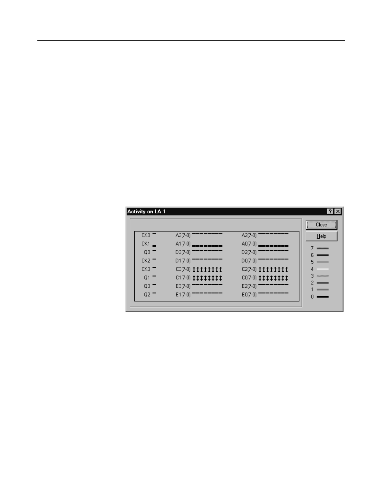
Functional Verification Procedures
2. Use the UP or DN buttons on the training board to select the PATTERN
GEN program.
3. Push the RUN button on the training board to start the pattern generator
program.
4. On the logic analyzer, restore the default setups (select Default System from
the File menu).
5. Open the Setup menu from the logic analyzer icon in the system menu.
6. Click on the Show Activity button to open the Activity monitor.
7. Check that the probe channels connected to the training board show activity
represented by up and down arrows for each channel.
Figure 5–1 shows an example of the Activity monitor with active signals for
the probes connected to the training board.
Figure 5–1: Sample Activity Monitor
If all signal channels show activity, you have verified the functionality of the
counter-pattern generator circuitry for the P6434 probe connections.
8. Disconnect the P6434 probes from the training board and from the logic
analyzer and connect the P6417 probes to the High Counter-Pattern
Generator and Low Counter-Pattern Generator connectors on the training
board (J840, J940, J830, and J930).
9. Check that the probe channels connected to the training board show activity
represented by up and down arrows for each channel.
TLA QuickStart Technical Reference Manual
5–3

Functional Verification Procedures
If all signal channels show activity, you have verified the functionality of the
counter-pattern generator circuitry for the P6417 probe connections.
10. Disconnect one of the P6417 probes and connect one set of the 8-channel
lead sets to the Setup-Hold Signal connector (J850).
11. Connect the other set of 8-channel lead sets to the Tapped Delay connector
(J950)
12. Check that the probe channels connected to the training board show activity
on each channel.
If all signal channels show activity, you have verified the functionality of the
Setup-Hold Signal connector and the Tapped Delay connector.
13. Disconnect the logic analyzer probes from the training board.
Digital and Analog Circuitry Check
The procedures in this section check the following signals on the training board:
Runt pulse and missing pulse
Narrow pulse
Burst pulse
Fast edge signal
Metastable glitch signal
Staircase signal
To complete these checks, you will need a 1 GHz analog bandwidth oscilloscope
and an oscilloscope probe (Tektronix TDS 684B with a P6345 probe).
5–4
TLA QuickStart Technical Reference Manual

Functional Verification Procedures
Runt Pulse and Missing
Pulse Check
Perform the followings steps to verify basic functionality of the runt pulse and
missing pulse.
1. Set up the vertical input of the oscilloscope to measure a 2 V pulse.
2. Set horizontal controls as follows:
Time/Div 100 ns
Position Trigger at center
Trigger position 50%
3. Set up the trigger controls as follows:
Type Pulse, Width, Neg, Trig Outside
15–128 ns
Level 3.2 V
Source Ch1
Polarity Positive
Threshold 220 mV
4. Connect the Channel 1 probe to the RUNT pin on the training board
(J870–3). Connect the probe ground lead to a nearby ground pin.
Narrow Pulse Check
5. Check for a series of pulses, with one of the pulses being a blinking runt
pulse.
Perform the followings steps to verify basic functionality of the narrow pulse
signal.
1. Set up the vertical input of the oscilloscope to measure a 500 mV signal.
2. Set horizontal controls as follows:
Time/Div 2 ns
Trigger position 50%
3. Set up the trigger controls as follows:
Type Edge
Source Ch1
Slope Rising
Level 500 mV
TLA QuickStart Technical Reference Manual
5–5

Functional Verification Procedures
4. Connect the Channel 1 probe to the PULS pin on the training board
5. Adjust the trigger level control on the oscilloscope for a positive pulse (the
6. Check for a 0.5 ns – 6.0 ns pulse with an amplitude between 0.3 V and
(J870–5). Connect the probe ground lead to a nearby ground pin.
pulse may have some jitter).
2.0 V.
Burst Pulse Check
Perform the followings steps to verify basic functionality of the burst pulse
signal.
1. Set up the vertical input of the oscilloscope to measure a 2 V signal.
2. Set horizontal controls as follows:
Time/Div 50 ns
Trigger position 50%
3. Set up the trigger controls as follows:
Type Edge
Source Ch1
Slope Rising
Level 3.2 V
4. Connect the Channel 1 probe to the BURST pin on the training board
(J860–3). Connect the probe ground lead to a nearby ground pin.
5. Adjust the trigger level control on the oscilloscope for a stable signal.
6. Check for a signal with bursts of pulses.
Fast Edge Signal Check
5–6
Perform the followings steps to verify basic functionality of the fast edge signal.
1. Set up the vertical input of the oscilloscope to measure a 200 mV signal. Set
the position two divisions below the center graticule.
2. Set horizontal controls as follows:
Time/Div 100 s
Position Trigger at center
Trigger position 50%
TLA QuickStart Technical Reference Manual

Functional Verification Procedures
3. Set up the trigger controls as follows:
Type Edge
Source Ch1
Slope Rising
Level 220 mV
4. Connect the Channel 1 probe to the EDGE pin on the training board
(J870–7). Connect the probe ground lead to a nearby ground pin.
5. Check for a signal from 250 mV to 1500 mV with a frequency from 1.5 KHz
to 3.5 KHz. The rise time should be from 0 to 300 ps.
Metastable Glitch Signal
Check
Perform the following steps to verify basic functionality of the metastable glitch
signal.
1. Set up the vertical input of the oscilloscope to measure a 2 V signal.
2. Set horizontal controls as follows:
Time/Div 20 ns
Position Trigger at center
Trigger position 50%
3. Set up the trigger controls as follows:
Type Edge
Source Ch1
Slope Rising
Polarity Positive
Level 1.3 V
Threshold 1.3 V
4. Connect the Channel 1 probe to the FF-D pin on the training board (J870–5).
Connect the probe ground lead to a nearby ground pin.
5. Check for a glitch in the square wave signal that is over 2 V.
TLA QuickStart Technical Reference Manual
5–7

Functional Verification Procedures
Staircase Signal Check
Perform the followings steps to verify basic functionality of the staircase signal.
1. Set up the vertical input of the oscilloscope to measure a 200 mV signal.
Set the position two divisions below the center graticule.
2. Set horizontal controls as follows:
Time/Div 1 ms
Position Trigger at center
Trigger position 90%
3. Set up the trigger controls as follows:
Mode Auto
Type Edge
Source Ch1
Slope Falling
Level 400 mV
4. Connect the Channel 1 probe to the STEP pin on the training board
(J870–1). Connect the probe ground lead to a nearby ground pin.
5. Adjust the oscilloscope trigger level control for a stable staircase signal.
6. Check for a staircase signal with a peak-to-peak amplitude between 800 mV
and 1200 mV and a frequency between 63 Hz and 250 Hz.
7. Disconnect the probes from the training board.
8. Power off the training board.
5–8
TLA QuickStart Technical Reference Manual

Maintenance
Preventing ESD
This chapter contains the information needed for periodic and corrective
maintenance of the TLA 7QS Training Board. The following sections are
included:
Preventing ESD
Service Strategy
Inspection and Cleaning (see page 6–2)
Troubleshooting (see page 6–3)
Repackaging Instructions (see page 6–3)
When performing any service adhere to the following precautions to avoid
damaging internal modules and their components due to electrostatic discharge
(ESD).
Service Strategy
Warranty Repair Service
1. Minimize handling of static-sensitive components.
2. Transport and store static-sensitive components in their static protected
containers or on a metal rail. Label any package that contains static-sensitive
components.
3. Discharge the static voltage from your body by wearing a grounded antistatic
wrist strap while handling these components.
4. Nothing capable of generating or holding a static charge should be allowed
on the work station surface.
Tektronix provides service to cover repair under warranty as well as other
services that may provide a cost-effective answer to your service needs.
Tektronix warrants the training board for three months from the date of
shipment. Any failures will be replaced with an exchange module from the
Beaverton Exchange center. Tektronix technicians provide in-service center
warranty service at most Tektronix service locations worldwide. For the latest
information on Tektronix products, refer to the Tektronix Internet site at
http://www.tek.com.
TLA QuickStart Technical Reference Manual
6–1

Maintenance
Customer site service is also available from most of the same service locations.
Repair or Calibration
Service
Self Service
Tektronix offers several standard-priced adjustment (calibration) and repair
services:
A single repair and/or adjustment
Calibrations using equipment and procedures that meet the traceability
standards specific to national standards requirements (Calibrations do not
apply to the TLA 7QS QuickStart Training Board)
Annual prearranged service do not apply to the TLA 7QS QuickStart
Training Board
Of these services, the annual prearranged service offers a particularly cost-effective approach to service for many owners of the TLA 700 series logic analyzers.
Tektronix supports repair to the module level by providing Module Exchange.
Module Exchange. Use this service to reduce down time for repair by exchanging
circuit boards for remanufactured ones. Tektronix ships an updated and tested
exchange circuit board from the Beaverton, Oregon service center. Each circuit
board comes with a 90-day service warranty.
Inspection and Cleaning
For More Information. Contact your local Tektronix service center or sales
engineer for more information on any of the repair or adjustment services just
described.
This section describes how to inspect for dirt and damage, and how to clean the
training board. Inspection and cleaning are done as preventive maintenance.
Preventive maintenance, when done regularly, may prevent malfunctions and
enhance reliability.
Preventive maintenance consists of visually inspecting and cleaning the training
board, and using general care when operating it. How often to do maintenance
depends on the severity of the environment in which the training board is used.
Inspect and clean the training board as often as operating conditions require.
Collection of dirt on internal components can cause them to overheat and break
down. Dirt acts as an insulating blanket, preventing efficient heat dissipation.
Dirt also provides an electrical conduction path
under high-humidity conditions.
that can cause failures, especially
6–2
TLA QuickStart Technical Reference Manual

CAUTION. Avoid using chemical cleaning agents that might damage the plastics
and external labels used on the training board. Use a cloth dampened with water
to clean external surfaces. Before using any cleaner, consult your Tektronix
Service Center or representative.
To clean the exterior, perform the following steps:
1. Remove loose dust on the outside of the training board with a lint free cloth.
2. Remove remaining dirt with a lint free cloth dampened with water. Do not
use abrasive cleaners.
Troubleshooting Procedures
Most troubleshooting is accomplished by use of diagnostics and probing for
signals on the training board with an oscilloscope, a logic analyzer, or a logic
probe.
Maintenance
Diagnostics
Signal Tracing
Parts Replacement
Diagnostics run when you first apply power to the training board or when you
press the Reset button. You can also select the diagnostics from the menu in the
user interface. For information on diagnostics refer to page 2–16.
Use an oscilloscope or a logic probe to trace faults to specific areas on the
training board. Use the schematics in this manual to help isolate problems to a
component or connector.
Refer to the Replaceable Electrical Parts list for part numbers of all electrical
parts on the training board. Refer to the Replaceable Mechanical Parts list for
part numbers of all mechanical parts and accessories.
Repackaging Instructions
This section contains the information needed to repackage the training board for
shipment.
If at all possible, use the original packaging to ship or store the training board. If
the original packaging is not available, use a corrugated cardboard shipping
carton having a test strength of at least 275 pounds (125 kg) and with an inside
dimension at least six inches (15.25 cm) greater than the training board
dimensions. Add cushioning material to prevent the training board from moving
around in the shipping container.
TLA QuickStart Technical Reference Manual
6–3

Maintenance
If the training board is being shipped to a Tektronix Service Center, enclose the
following information:
The owner’s address
Name and phone number of a contact person
Type and serial number of the training board
Reason for returning
A complete description of the service required
Seal the shipping carton with an industrial stapler or strapping tape.
Mark the address of the Tektronix Service Center and also your own return
address on the shipping carton in two prominent locations.
6–4
TLA QuickStart Technical Reference Manual

Replaceable Electrical Parts
This section contains a list of the electrical components for the TLA 7QS
training board. Use this list to identify and order replacement parts.
Parts Ordering Information
Replacement parts are available through your local Tektronix field office or
representative.
Changes to Tektronix products are sometimes made to accommodate improved
components as they become available and to give you the benefit of the latest
improvements. Therefore, when ordering parts, it is important to include the
following information in your order:
Part number
Instrument type or model number
Instrument serial number
Instrument modification number, if applicable
If you order a part that has been replaced with a different or improved part, your
local Tektronix field office or representative will contact you concerning any
change in part number.
Change information, if any, is located at the rear of this manual.
Using the Replaceable Electrical Parts List
The tabular information in the Replaceable Electrical Parts List is arranged for
quick retrieval. Understanding the structure and features of the list will help you
find all of the information you need for ordering replacement parts. The
following table describes each column of the electrical parts list.
TLA QuickStart Technical Reference Manual
7–1
Replaceable Electrical Parts
Parts list column descriptions
Column Column name Description
1 Component number The component number appears on diagrams and circuit board illustrations, located in the diagrams
section. Assembly numbers are clearly marked on each diagram and circuit board illustration in the
Diagrams section, and on the mechanical exploded views in the Replaceable Mechanical Parts list
section. The component number is obtained by adding the assembly number prefix to the circuit
number (see Component Number illustration following this table).
The electrical parts list is arranged by assemblies in numerical sequence (A1, with its subassemblies and parts, precedes A2, with its subassemblies and parts).
Chassis-mounted parts have no assembly number prefix, and they are located at the end of the
electrical parts list.
2 Tektronix part number Use this part number when ordering replacement parts from Tektronix.
3 and 4 Serial number Column three indicates the serial number at which the part was first effective. Column four indicates
the serial number at which the part was discontinued. No entry indicates the part is good for all
serial numbers.
5 Name & description An item name is separated from the description by a colon (:). Because of space limitations, an item
name may sometimes appear as incomplete. Use the U.S. Federal Catalog handbook H6-1 for
further item name identification.
6 Mfr. code This indicates the code number of the actual manufacturer of the part.
7 Mfr. part number This indicates the actual manufacturer’s or vendor’s part number.
Abbreviations
Component Number
List of Assemblies
Chassis Parts
Mfr. Code to Manufacturer
Cross Index
Abbreviations conform to American National Standard ANSI Y1.1–1972.
Component Number
A23A2R1234 A23 R1234
Assembly number Circuit Number
Read: Resistor 1234 (of Subassembly 2) of Assembly 23
A2
Subassembly Number
(optional)
A list of assemblies is located at the beginning of the electrical parts list. The
assemblies are listed in numerical order. When a part’s complete component
number is known, this list will identify the assembly in which the part is located.
Chassis-mounted parts and cable assemblies are located at the end of the
Replaceable Electrical Parts List.
The table titled Manufacturers Cross Index shows codes, names, and addresses
of manufacturers or vendors of components listed in the parts list.
7–2
TLA QuickStart Technical Reference Manual

Replaceable Electrical Parts
Manufacturers cross index
Mfr.
code
00779 AMP INC. CUSTOMER SERVICE DEPT
01295 TEXAS INSTRUMENTS INC SEMICONDUCTOR GROUP
04222 AVX/KYOCERA PO BOX 867 MYRTLE BEACH, SC 29577
04426 ITW SWITCHES AN ILLINOIS TOOL WORKS CO.
04713 MOTOROLA INC SEMICONDUCTOR PRODUCTS SECTOR
06090 RAYCHEM CORP 300 CONSTITUTION DR MENLO PARK, CA 94025–1111
09969 DALE ELECTRONIC COMPONENTS EAST HWY 50
0B0A9 DALLAS SEMICONDUCTOR 4350 BELTWOOD PKWY S DALLAS, TX 75244
0HAF7 EPSON AMERICA 20770 MADRONA AVE TORRANCE, CA 90503
0LUT2 TOYOCOM USA INC 617 E GOLF ROAD
1CH66 PHILIPS SEMICONDUCTORS 811 E ARQUES AVE
1ES66 MAXIM INTEGRATED PRODUCTS INC 120 SAN GABRIEL DR SUNNYVALE, CA 94086
27014 NATIONAL SEMICONDUCTOR CORP 2900 SEMICONDUCTOR DR
29454 JOHANSON DIELECTRICS INC 15191 BLEDSOE STREET SYLMAR, CA 91342
31918 ITT SWITCH PRODUCTS 8081 WALLACE RD EDEN PRAIRIE, MN 55344–8798
34335 ADVANCED MICRO DEVICES INC ONE AMD PLACE
50139 ALLEN–BRADLEY COMPANY INC ELECTRONIC COMPONENTS DIVISION
50434 HEWLETT PACKARD 370 W TRIMBLE ROAD SAN JOSE, CA 95131–1008
53387 3M COMPANY ELECTRONICS PRODUCTS DIV
55680 NICHICON (AMERICA) CORP 927 E STATE PARKWA Y SCHAUMBURG, IL 60195–4526
57924 BOURNS INC INTEGRATED TECHNOLOGY DIV.
59124 KOA SPEER ELECTRONICS INC BOLIV AR DRIVE
60395 XICOR INC 851 BUCKEYE CT MILPITAS, CA 95035–7408
61429 FOX ELECTRONICS DIV OF FOX ENTERPRIXED INC
62712 SEIKO INSTRUMENTS USA INC ELECTRONIC COMPONENTS DIV
62786 HITACHI AMERICA LTD HITACHI PLAZA
63058 BERG ELECTRONICS INC. MCKENZIE SOCKET DIV
64155 LINEAR TECHNOLOGY CORP. 1630 MCCARTHY BOULEVARD MILPITAS, CA 950357487
Manufacturer Address City, state, zip code
PO BOX 3608
13500 N CENTRAL EXPRESSWA Y
PO BOX 655303
6615 W. IRVING PARK RD.
5005 E MCDOWELL ROAD
P.O. BOX 180
SUITE 172
PO BOX 3409
PO BOX 58090 MS 30–115
PO BOX 3453
1414 ALLEN BRADLEY DRIVE
3M AUSTIN CENTER
1400 NORTH 1000 WEST
PO BOX 547
5842 CORPORATION CIRCLE
2990 W LOMITA BLVD
2000 SIERRA POINT PKWY
910 PAGE AVE
HARRISBURG, PA 17105–3608
DALLAS, TX 75272–5303
CHICAGO, IL 60634
PHOENIX, AZ 85008–4229
YANKTON, SD 57078
ARLINGTON HEIGHTS, IL 60005
SUNNYVALE, CA 94086–3409
SANTA CLARA, CA 95051–0606
SUNNYVALE, CA 94088–3453
EL PASO, TX 79936
AUSTIN, TX 78769–2963
LOGAN, UT 84321
BRADFORD, PA 16701
FORT MEYERS, FL 33905
TORRANCE, CA 90505
BRISBAINE, CA 94005
FREMONT , CA 94538–7340
TLA QuickStart Technical Reference Manual
7–3

Replaceable Electrical Parts
Manufacturers cross index (Cont.)
Mfr.
code
76493 BELL INDUSTRIES JW MILLER DIVISION
80009 TEKTRONIX INC 14150 SW KARL BRAUN DR
91637 DALE ELECTRONIC COMPONENTS 1122 23RD ST COLUMBUS, NE 68601
TK2449 SINGATRON ENTERPRISE CO LTD 13925 MAGNOLIA AVE CHINO, CA 91710
306 E ALONDRA BLVD
PO BOX 2859
PO BOX 500
City , state, zip codeAddressManufacturer
GARDENA, CA 90247–1059
BEAVERT ON, OR 97077–0001
7–4
TLA QuickStart Technical Reference Manual

Replaceable electrical parts list
Replaceable Electrical Parts
Component
number
A01 671–3684–00 CIRCUIT BOARD:LA QUICKSTART 80009 671–3684–00
A01C130 283–5353–00 CAP,FXD,CERAMIC:0.1UF,20%,16V,X7R,0603,SMD,T&R 04222 0603YC104MAT2A
A01C150 283–5353–00 CAP,FXD,CERAMIC:0.1UF,20%,16V,X7R,0603,SMD,T&R 04222 0603YC104MAT2A
A01C0151 283–5353–00 CAP,FXD,CERAMIC:0.1UF,20%,16V,X7R,0603,SMD,T&R 04222 0603YC104MAT2A
A01C160 283–5353–00 CAP,FXD,CERAMIC:0.1UF,20%,16V,X7R,0603,SMD,T&R 04222 0603YC104MAT2A
A01C170 283–5353–00 CAP,FXD,CERAMIC:0.1UF,20%,16V,X7R,0603,SMD,T&R 04222 0603YC104MAT2A
A01C180 283–5353–00 CAP,FXD,CERAMIC:0.1UF,20%,16V,X7R,0603,SMD,T&R 04222 0603YC104MAT2A
A01C210 283–5114–00 CAP,FXD,CERAMIC:MLC,0.1UF,10%,50V ,X7R,1206,SMD,8MM
A01C211 290–0973–00 CAP ,FXD,ELCTLT:100UF,20%,25VDC ALUMINUM 55680 UVX1V101MPA
A01C212 283–5114–00 CAP,FXD,CERAMIC:MLC,0.1UF,10%,50V ,X7R,1206,SMD,8MM
A01C213 290–0973–00 CAP ,FXD,ELCTLT:100UF,20%,25VDC ALUMINUM 55680 UVX1V101MPA
A01C0240 283–5353–00 CAP,FXD,CERAMIC:0.1UF,20%,16V,X7R,0603,SMD,T&R 04222 0603YC104MAT2A
A01C0260 283–5353–00 CAP,FXD,CERAMIC:0.1UF,20%,16V,X7R,0603,SMD,T&R 04222 0603YC104MAT2A
A01C0270 283–5353–00 CAP,FXD,CERAMIC:0.1UF,20%,16V,X7R,0603,SMD,T&R 04222 0603YC104MAT2A
A01C0271 283–5353–00 CAP,FXD,CERAMIC:0.1UF,20%,16V,X7R,0603,SMD,T&R 04222 0603YC104MAT2A
A01C0280 283–5353–00 CAP,FXD,CERAMIC:0.1UF,20%,16V,X7R,0603,SMD,T&R 04222 0603YC104MAT2A
A01C0281 283–5353–00 CAP,FXD,CERAMIC:0.1UF,20%,16V,X7R,0603,SMD,T&R 04222 0603YC104MAT2A
A01C282 283–5353–00 CAP ,FXD,CERAMIC:0.1UF,20%,16V ,X7R,0603,SMD,T&R 04222 0603YC104MA T2A
A01C0283 283–5353–00 CAP,FXD,CERAMIC:0.1UF,20%,16V,X7R,0603,SMD,T&R 04222 0603YC104MAT2A
A01C0284 283–5353–00 CAP,FXD,CERAMIC:0.1UF,20%,16V,X7R,0603,SMD,T&R 04222 0603YC104MAT2A
A01C285 283–5353–00 CAP ,FXD,CERAMIC:0.1UF,20%,16V ,X7R,0603,SMD,T&R 04222 0603YC104MA T2A
A01C350 283–5353–00 CAP ,FXD,CERAMIC:0.1UF,20%,16V ,X7R,0603,SMD,T&R 04222 0603YC104MA T2A
A01C370 283–5353–00 CAP ,FXD,CERAMIC:0.1UF,20%,16V ,X7R,0603,SMD,T&R 04222 0603YC104MA T2A
A01C0410 290–5051–00 CAP,FXD,TANT:DRY,100UF,20%,16V,0.287 X 0.169,7343H,
A01C411 290–5051–00 CAP ,FXD,TANT:DRY,100UF,20%,16V,0.287 X 0.169,7343H,SMD,
A01C0420 290–5051–00 CAP,FXD,TANT:DRY,100UF,20%,16V,0.287 X 0.169,7343H,SMD,
A01C421 283–5353–00 CAP ,FXD,CERAMIC:0.1UF,20%,16V ,X7R,0603,SMD,T&R 04222 0603YC104MA T2A
A01C0422 283–5353–00 CAP,FXD,CERAMIC:0.1UF,20%,16V,X7R,0603,SMD,T&R 04222 0603YC104MAT2A
A01C0460 283–5353–00 CAP,FXD,CERAMIC:0.1UF,20%,16V,X7R,0603,SMD,T&R 04222 0603YC104MAT2A
A01C0461 283–5353–00 CAP,FXD,CERAMIC:0.1UF,20%,16V,X7R,0603,SMD,T&R 04222 0603YC104MAT2A
A01C0462 283–5353–00 CAP,FXD,CERAMIC:0.1UF,20%,16V,X7R,0603,SMD,T&R 04222 0603YC104MAT2A
A01C470 283–5353–00 CAP ,FXD,CERAMIC:0.1UF,20%,16V ,X7R,0603,SMD,T&R 04222 0603YC104MA T2A
A01C471 283–5267–00 CAP ,FXD,CERAMIC:MLC,1UF,+80%–20%,25V ,Y5V,1206,SMD,T&R 04222 12063G105ZAT4A
A01C472 283–5353–00 CAP ,FXD,CERAMIC:0.1UF,20%,16V ,X7R,0603,SMD,T&R 04222 0603YC104MA T2A
Tektronix
part number
Serial no.
effective
Serial no.
discont’d
Name & description
T&R
T&R
SMD,T&R
T&R
T&R
Mfr.
code
04222 12065C104KAT(1A
04222 12065C104KAT(1A
04222 TAJE107M016R
04222 TAJE107M016R
04222 TAJE107M016R
Mfr. part number
OR 3A)
OR 3A)
TLA QuickStart Technical Reference Manual
7–5

Replaceable Electrical Parts
Replaceable electrical parts list (Cont.)
Component
number
A01C480 283–5353–00 CAP,FXD,CERAMIC:0.1UF,20%,16V,X7R,0603,SMD,T&R 04222 0603YC104MAT2A
A01C0481 283–5353–00 CAP,FXD,CERAMIC:0.1UF,20%,16V,X7R,0603,SMD,T&R 04222 0603YC104MAT2A
A01C482 283–5353–00 CAP,FXD,CERAMIC:0.1UF,20%,16V,X7R,0603,SMD,T&R 04222 0603YC104MAT2A
A01C483 283–5353–00 CAP,FXD,CERAMIC:0.1UF,20%,16V,X7R,0603,SMD,T&R 04222 0603YC104MAT2A
A01C0484 283–5353–00 CAP,FXD,CERAMIC:0.1UF,20%,16V,X7R,0603,SMD,T&R 04222 0603YC104MAT2A
A01C485 283–5353–00 CAP,FXD,CERAMIC:0.1UF,20%,16V,X7R,0603,SMD,T&R 04222 0603YC104MAT2A
A01C0520 283–5353–00 CAP,FXD,CERAMIC:0.1UF,20%,16V,X7R,0603,SMD,T&R 04222 0603YC104MAT2A
A01C0521 283–5267–00 CAP,FXD,CERAMIC:MLC,1UF,+80%–20%,25V,Y5V,1206,SMD,T&R 04222 12063G105ZAT4A
A01C0522 283–5267–00 CAP,FXD,CERAMIC:MLC,1UF,+80%–20%,25V,Y5V,1206,SMD,T&R 04222 12063G105ZAT4A
A01C0523 283–5267–00 CAP,FXD,CERAMIC:MLC,1UF,+80%–20%,25V,Y5V,1206,SMD,T&R 04222 12063G105ZAT4A
A01C550 283–5353–00 CAP,FXD,CERAMIC:0.1UF,20%,16V,X7R,0603,SMD,T&R 04222 0603YC104MAT2A
A01C551 283–5353–00 CAP,FXD,CERAMIC:0.1UF,20%,16V,X7R,0603,SMD,T&R 04222 0603YC104MAT2A
A01C560 283–5353–00 CAP,FXD,CERAMIC:0.1UF,20%,16V,X7R,0603,SMD,T&R 04222 0603YC104MAT2A
A01C0561 283–5353–00 CAP,FXD,CERAMIC:0.1UF,20%,16V,X7R,0603,SMD,T&R 04222 0603YC104MAT2A
A01C0562 283–5353–00 CAP,FXD,CERAMIC:0.1UF,20%,16V,X7R,0603,SMD,T&R 04222 0603YC104MAT2A
A01C0563 283–5353–00 CAP,FXD,CERAMIC:0.1UF,20%,16V,X7R,0603,SMD,T&R 04222 0603YC104MAT2A
A01C0564 283–5353–00 CAP,FXD,CERAMIC:0.1UF,20%,16V,X7R,0603,SMD,T&R 04222 0603YC104MAT2A
A01C565 283–5353–00 CAP,FXD,CERAMIC:0.1UF,20%,16V,X7R,0603,SMD,T&R 04222 0603YC104MAT2A
A01C570 283–5353–00 CAP,FXD,CERAMIC:0.1UF,20%,16V,X7R,0603,SMD,T&R 04222 0603YC104MAT2A
A01C0571 283–5353–00 CAP,FXD,CERAMIC:0.1UF,20%,16V,X7R,0603,SMD,T&R 04222 0603YC104MAT2A
A01C572 283–5114–00 CAP,FXD,CERAMIC:MLC,0.1UF,10%,50V,X7R,1206,SMD,8MM
A01C573 283–5196–00 CAP,FXD,CERAMIC:MLC,47PF,5%,100V,NPO,1206,SMD,8MM
A01C0574 283–5353–00 CAP,FXD,CERAMIC:0.1UF,20%,16V,X7R,0603,SMD,T&R 04222 0603YC104MAT2A
A01C0575 283–5353–00 CAP,FXD,CERAMIC:0.1UF,20%,16V,X7R,0603,SMD,T&R 04222 0603YC104MAT2A
A01C576 283–5353–00 CAP,FXD,CERAMIC:0.1UF,20%,16V,X7R,0603,SMD,T&R 04222 0603YC104MAT2A
A01C580 283–5353–00 CAP,FXD,CERAMIC:0.1UF,20%,16V,X7R,0603,SMD,T&R 04222 0603YC104MAT2A
A01C0581 283–5353–00 CAP,FXD,CERAMIC:0.1UF,20%,16V,X7R,0603,SMD,T&R 04222 0603YC104MAT2A
A01C582 283–5353–00 CAP,FXD,CERAMIC:0.1UF,20%,16V,X7R,0603,SMD,T&R 04222 0603YC104MAT2A
A01C0583 283–5353–00 CAP,FXD,CERAMIC:0.1UF,20%,16V,X7R,0603,SMD,T&R 04222 0603YC104MAT2A
A01C584 283–5353–00 CAP,FXD,CERAMIC:0.1UF,20%,16V,X7R,0603,SMD,T&R 04222 0603YC104MAT2A
A01C586 283–5017–00 CAP,FXD,CERAMIC:MLC,1PF,+/–0.25PF,50V,NPO,1206,SMD,8MM
A01C600 283–5353–00 CAP,FXD,CERAMIC:0.1UF,20%,16V,X7R,0603,SMD,T&R 04222 0603YC104MAT2A
A01C610 283–5353–00 CAP,FXD,CERAMIC:0.1UF,20%,16V,X7R,0603,SMD,T&R 04222 0603YC104MAT2A
A01C0611 283–5353–00 CAP,FXD,CERAMIC:0.1UF,20%,16V,X7R,0603,SMD,T&R 04222 0603YC104MAT2A
A01C0612 283–5353–00 CAP,FXD,CERAMIC:0.1UF,20%,16V,X7R,0603,SMD,T&R 04222 0603YC104MAT2A
A01C0620 283–5267–00 CAP,FXD,CERAMIC:MLC,1UF,+80%–20%,25V,Y5V,1206,SMD,T&R 04222 12063G105ZAT4A
Tektronix
part number
Serial no.
effective
Serial no.
discont’d
Name & description
T&R
T&R
T&R
Mfr.
code
04222 12065C104KAT(1A
04222 12061A470JAT1A
04222 12065A1R0CAT1A
Mfr. part number
OR 3A)
7–6
TLA QuickStart Technical Reference Manual

Replaceable electrical parts list (Cont.)
Replaceable Electrical Parts
Component
number
A01C0621 283–5353–00 CAP,FXD,CERAMIC:0.1UF,20%,16V,X7R,0603,SMD,T&R 04222 0603YC104MAT2A
A01C622 283–5353–00 CAP,FXD,CERAMIC:0.1UF,20%,16V,X7R,0603,SMD,T&R 04222 0603YC104MAT2A
A01C650 283–5353–00 CAP,FXD,CERAMIC:0.1UF,20%,16V,X7R,0603,SMD,T&R 04222 0603YC104MAT2A
A01C0660 283–5353–00 CAP,FXD,CERAMIC:0.1UF,20%,16V,X7R,0603,SMD,T&R 04222 0603YC104MAT2A
A01C661 283–5334–00 CAP ,FXD CERAMIC:MLC,10PF,5%,100V,NPO,0603,SMD,T&R. 29454 250R14N100CV4T
A01C670 283–5334–00 CAP ,FXD CERAMIC:MLC,10PF,5%,100V,NPO,0603,SMD,T&R. 29454 250R14N100CV4T
A01C671 283–5353–00 CAP ,FXD,CERAMIC:0.1UF,20%,16V,X7R,0603,SMD,T&R 04222 0603YC104MA T2A
A01C672 283–5358–00 CAP ,FXD,CERAMIC:100PF,5%,100V,NPO,0603,SMD,T&R 04222 06031A101JAT2A
A01C0673 283–5353–00 CAP,FXD,CERAMIC:0.1UF ,20%,16V,X7R,0603,SMD,T&R 04222 0603YC104MAT2A
A01C680 283–5353–00 CAP ,FXD,CERAMIC:0.1UF,20%,16V,X7R,0603,SMD,T&R 04222 0603YC104MA T2A
A01C710 283–5353–00 CAP ,FXD,CERAMIC:0.1UF,20%,16V,X7R,0603,SMD,T&R 04222 0603YC104MA T2A
A01C0711 283–5353–00 CAP,FXD,CERAMIC:0.1UF ,20%,16V,X7R,0603,SMD,T&R 04222 0603YC104MAT2A
A01C712 283–5353–00 CAP ,FXD,CERAMIC:0.1UF,20%,16V,X7R,0603,SMD,T&R 04222 0603YC104MA T2A
A01C713 283–5353–00 CAP ,FXD,CERAMIC:0.1UF,20%,16V,X7R,0603,SMD,T&R 04222 0603YC104MA T2A
A01C0714 283–5353–00 CAP,FXD,CERAMIC:0.1UF ,20%,16V,X7R,0603,SMD,T&R 04222 0603YC104MAT2A
A01C720 283–5353–00 CAP ,FXD,CERAMIC:0.1UF,20%,16V,X7R,0603,SMD,T&R 04222 0603YC104MA T2A
A01C0721 283–5353–00 CAP,FXD,CERAMIC:0.1UF ,20%,16V,X7R,0603,SMD,T&R 04222 0603YC104MAT2A
A01C0722 283–5353–00 CAP,FXD,CERAMIC:0.1UF ,20%,16V,X7R,0603,SMD,T&R 04222 0603YC104MAT2A
A01C723 283–5353–00 CAP ,FXD,CERAMIC:0.1UF,20%,16V,X7R,0603,SMD,T&R 04222 0603YC104MA T2A
A01C0724 283–5353–00 CAP,FXD,CERAMIC:0.1UF ,20%,16V,X7R,0603,SMD,T&R 04222 0603YC104MAT2A
A01C0725 283–5353–00 CAP,FXD,CERAMIC:0.1UF ,20%,16V,X7R,0603,SMD,T&R 04222 0603YC104MAT2A
A01C0790 283–5353–00 CAP,FXD,CERAMIC:0.1UF ,20%,16V,X7R,0603,SMD,T&R 04222 0603YC104MAT2A
A01C0791 283–5353–00 CAP,FXD,CERAMIC:0.1UF ,20%,16V,X7R,0603,SMD,T&R 04222 0603YC104MAT2A
A01C800 283–5353–00 CAP ,FXD,CERAMIC:0.1UF,20%,16V,X7R,0603,SMD,T&R 04222 0603YC104MA T2A
A01C810 283–5353–00 CAP ,FXD,CERAMIC:0.1UF,20%,16V,X7R,0603,SMD,T&R 04222 0603YC104MA T2A
A01C811 283–5353–00 CAP ,FXD,CERAMIC:0.1UF,20%,16V,X7R,0603,SMD,T&R 04222 0603YC104MA T2A
A01C0812 283–5353–00 CAP,FXD,CERAMIC:0.1UF ,20%,16V,X7R,0603,SMD,T&R 04222 0603YC104MAT2A
A01C813 283–5353–00 CAP ,FXD,CERAMIC:0.1UF,20%,16V,X7R,0603,SMD,T&R 04222 0603YC104MA T2A
A01C820 283–5353–00 CAP ,FXD,CERAMIC:0.1UF,20%,16V,X7R,0603,SMD,T&R 04222 0603YC104MA T2A
A01C0821 283–5353–00 CAP,FXD,CERAMIC:0.1UF ,20%,16V,X7R,0603,SMD,T&R 04222 0603YC104MAT2A
A01C822 283–5353–00 CAP ,FXD,CERAMIC:0.1UF,20%,16V,X7R,0603,SMD,T&R 04222 0603YC104MA T2A
A01C890 283–5353–00 CAP ,FXD,CERAMIC:0.1UF,20%,16V,X7R,0603,SMD,T&R 04222 0603YC104MA T2A
A01C0891 283–5353–00 CAP,FXD,CERAMIC:0.1UF ,20%,16V,X7R,0603,SMD,T&R 04222 0603YC104MAT2A
A01C0910 283–5353–00 CAP,FXD,CERAMIC:0.1UF ,20%,16V,X7R,0603,SMD,T&R 04222 0603YC104MAT2A
A01C911 283–5353–00 CAP ,FXD,CERAMIC:0.1UF,20%,16V,X7R,0603,SMD,T&R 04222 0603YC104MA T2A
A01C0920 283–5353–00 CAP,FXD,CERAMIC:0.1UF ,20%,16V,X7R,0603,SMD,T&R 04222 0603YC104MAT2A
A01C921 283–5353–00 CAP ,FXD,CERAMIC:0.1UF,20%,16V,X7R,0603,SMD,T&R 04222 0603YC104MA T2A
A01C990 283–5353–00 CAP ,FXD,CERAMIC:0.1UF,20%,16V,X7R,0603,SMD,T&R 04222 0603YC104MA T2A
Tektronix
part number
Serial no.
effective
Serial no.
discont’d
Name & description
Mfr.
code
Mfr. part number
TLA QuickStart Technical Reference Manual
7–7

Replaceable Electrical Parts
Replaceable electrical parts list (Cont.)
Component
number
A01C0214 283–5114–00 CAP,FXD,CERAMIC:MLC,0.1UF,10%,50V,X7R,1206,SMD,8MM
A01CR120 152–5084–00 DIODE,RECT:SCHTKY,40V,3A,80A
A01CR220 152–5084–00 DIODE,RECT:SCHTKY,40V,3A,80A
A01CR0310 152–5084–00 DIODE,RECT:SCHTKY ,40V ,3A,80A
A01CR670 152–5047–00 DIODE,SIG:ULTRA FAST,DUAL,COMMON
A01CR671 152–5047–00 DIODE,SIG:ULTRA FAST,DUAL,COMMON
A01CR800 152–0843–00 DIODE,SIG:SCHTKY,SER–PAIR,20V,410MV,1.3PF,HSMS–2812,SO
A01CR801 152–0843–00 DIODE,SIG:SCHTKY,SER–PAIR,20V,410MV,1.3PF,HSMS–2812,SO
A01DS210 150–1132–00 DIODE,OPTO:LED,GRN,569MCD,10.6MCD AT 10MA,40 DEG
A01DS780 150–1137–00 DIODE,OPTO:LED,BAR GRAPH
A01DS880 150–1137–00 DIODE,OPTO:LED,BAR GRAPH
Tektronix
part number
Serial no.
effective
Serial no.
discont’d
Name & description
T&R
IFSM,MBRS340,DO–214AB/SMC,16MM T&R
IFSM,MBRS340,DO–214AB/SMC,16MM T&R
IFSM,MBRS340,DO–214AB/SMC,16MM T&R
CATHODE,100V,0.74VF,4NS,2.0PF,MMBD1204,TO–236/SOT–23,8
MM
CATHODE,100V,0.74VF,4NS,2.0PF,MMBD1204,TO–236/SOT–23,8
MM
T–23,T&R
T–23,T&R
VIEW ANGL,HLMP–3568,T–1 3/4,LOW PROFILE
ARRAY,MULTI–COLOR,10–ELEMENT
ARRAY,MULTI–COLOR,10–ELEMENT
Mfr.
code
04222 12065C104KAT(1A
04713 MBRS340T3
04713 MBRS340T3
04713 MBRS340T3
27014 MMBD1204
27014 MMBD1204
50434 HSMS–2812–T31
50434 HSMS–2812–T31
50434 HLMP–3568
50434 HDSP–4836
50434 HDSP–4836
Mfr. part number
OR 3A)
A01F220 159–5008–00 FUSE,THRM,CHIP:SELF RESETTING FUSE,1.5A HOLD,3.0A
A01J111 131–5527–00 JACK,POWER DC:PCB,MALE,R TANG,2MM PIN,11MM H(0.433) X
A01J180 131–3692–00 CONN,DIN:PCB,MALE,RTANG,3 X 32,0.1CTR,0.209 MLG X 0.104
A01J200 131–3358–00 CONN,HDR:PCB,MALE,RTANG,2 X 5,0.1 CTR,0.390 MLG X 0.112
A01J320 131–6134–00 CONN,PLUG:SMD,MICT OR,PCB,FEMALE,STR,38 POS,0.025
A01J330 131–4917–00 CONN,HDR:PCB,MALE,STR,1 X 2,0.1 CTR,0.235 MLG X 0.110
A01J340 131–4917–00 CONN,HDR:PCB,MALE,STR,1 X 2,0.1 CTR,0.235 MLG X 0.110
A01J350 131–4917–00 CONN,HDR:PCB,MALE,STR,1 X 2,0.1 CTR,0.235 MLG X 0.110
A01J400 131–3395–00 CONN,DSUB:PCB,MALE,RTANG,25 POS,0.318 MLG X 0.125
A01J420 131–6134–00 CONN,PLUG:SMD,MICT OR,PCB,FEMALE,STR,38 POS,0.025
7–8
TRIP AT 20 DEG C,30V MAX,SMD150
3.5MM(0.137) TAIL,9MM(0.354) W ,TIN,W/SWI
TAIL0.437 H,BD RETENTION,HIGH TE
TAIL,0.33 H,SHRD/4 SIDES,MIL PLZ
CTR,0.245 H,GOLD
TAIL,30 GOLD,TUBE,HIGH TEMP,
TAIL,30 GOLD,TUBE,HIGH TEMP,
TAIL,30 GOLD,TUBE,HIGH TEMP,
TAIL,30 GOLD,W/4–40 THD INSERTS,BD RETE
CTR,0.245 H,GOLD
TLA QuickStart Technical Reference Manual
06090 SMD150–2
TK2449 DJ–005–A
00779 536416–5
53387 2510–5002UB
00779 767004–1
00779 104350–1
00779 104350–1
00779 104350–1
00779 747842–4
00779 767004–1

Replaceable electrical parts list (Cont.)
Replaceable Electrical Parts
Component
number
A01J430 131–5267–00 CONN,HDR:PCB,MALE,STR,2 X 40,0.1 CTR,0.235 MLG X 0.110
A01J440 131–5267–00 CONN,HDR:PCB,MALE,STR,2 X 40,0.1 CTR,0.235 MLG X 0.110
A01J450 131–5267–00 CONN,HDR:PCB,MALE,STR,2 X 40,0.1 CTR,0.235 MLG X 0.110
A01J500 131–3925–00 CONN,DSUB:PCB,FEMALE,RTANG,9 POS,0.112 CTR,0.318 MLG
A01J530 131–5267–00 CONN,HDR:PCB,MALE,STR,2 X 40,0.1 CTR,0.235 MLG X 0.110
A01J531 131–4917–00 CONN,HDR:PCB,MALE,STR,1 X 2,0.1 CTR,0.235 MLG X 0.110
A01J540 131–5267–00 CONN,HDR:PCB,MALE,STR,2 X 40,0.1 CTR,0.235 MLG X 0.110
A01J541 131–4917–00 CONN,HDR:PCB,MALE,STR,1 X 2,0.1 CTR,0.235 MLG X 0.110
A01J550 131–5267–00 CONN,HDR:PCB,MALE,STR,2 X 40,0.1 CTR,0.235 MLG X 0.110
A01J551 131–4917–00 CONN,HDR:PCB,MALE,STR,1 X 2,0.1 CTR,0.235 MLG X 0.110
A01J600 131–3358–00 CONN,HDR:PCB,MALE,RTANG,2 X 5,0.1 CTR,0.390 MLG X 0.112
A01J620 131–6134–00 CONN,PLUG:SMD,MICT OR,PCB,FEMALE,STR,38 POS,0.025
A01J630 131–5267–00 CONN,HDR:PCB,MALE,STR,2 X 40,0.1 CTR,0.235 MLG X 0.110
A01J640 131–5267–00 CONN,HDR:PCB,MALE,STR,2 X 40,0.1 CTR,0.235 MLG X 0.110
A01J650 131–5267–00 CONN,HDR:PCB,MALE,STR,2 X 40,0.1 CTR,0.235 MLG X 0.110
A01J700 131–5999–00 CONN,RF:BNC,FEMALE,50 OHM,RT ANG,PCB,0.340 H X 0.110
A01J730 131–5267–00 CONN,HDR:PCB,MALE,STR,2 X 40,0.1 CTR,0.235 MLG X 0.110
A01J731 131–4917–00 CONN,HDR:PCB,MALE,STR,1 X 2,0.1 CTR,0.235 MLG X 0.110
A01J740 131–5267–00 CONN,HDR:PCB,MALE,STR,2 X 40,0.1 CTR,0.235 MLG X 0.110
A01J741 131–4917–00 CONN,HDR:PCB,MALE,STR,1 X 2,0.1 CTR,0.235 MLG X 0.110
A01J750 131–5267–00 CONN,HDR:PCB,MALE,STR,2 X 40,0.1 CTR,0.235 MLG X 0.110
A01J751 131–4917–00 CONN,HDR:PCB,MALE,STR,1 X 2,0.1 CTR,0.235 MLG X 0.110
A01J760 131–4917–00 CONN,HDR:PCB,MALE,STR,1 X 2,0.1 CTR,0.235 MLG X 0.110
Tektronix
part number
Serial no.
effective
Serial no.
discont’d
Name & description
TAIL,30GOLD, HIGH TEMP,
TAIL,30GOLD, HIGH TEMP,
TAIL,30GOLD, HIGH TEMP,
X 0.125 TAIL,4–40 THD INSERT,BD RETE
TAIL,30GOLD, HIGH TEMP,
TAIL,30 GOLD,TUBE,HIGH TEMP,
TAIL,30GOLD, HIGH TEMP,
TAIL,30 GOLD,TUBE,HIGH TEMP,
TAIL,30GOLD, HIGH TEMP,
TAIL,30 GOLD,TUBE,HIGH TEMP,
TAIL,0.33 H,SHRD/4 SIDES,MIL PLZ
CTR,0.245 H,GOLD
TAIL,30GOLD, HIGH TEMP,
TAIL,30GOLD, HIGH TEMP,
TAIL,30GOLD, HIGH TEMP,
TAIL,W/O MTG THD,NICKEL PL DIECAST/
TAIL,30GOLD, HIGH TEMP,
TAIL,30 GOLD,TUBE,HIGH TEMP,
TAIL,30GOLD, HIGH TEMP,
TAIL,30 GOLD,TUBE,HIGH TEMP,
TAIL,30GOLD, HIGH TEMP,
TAIL,30 GOLD,TUBE,HIGH TEMP,
TAIL,30 GOLD,TUBE,HIGH TEMP,
Mfr.
code
00779 104326–4
00779 104326–4
00779 104326–4
00779 747844–4
00779 104326–4
00779 104350–1
00779 104326–4
00779 104350–1
00779 104326–4
00779 104350–1
53387 2510–5002UB
00779 767004–1
00779 104326–4
00779 104326–4
00779 104326–4
00779 414373–1
00779 104326–4
00779 104350–1
00779 104326–4
00779 104350–1
00779 104326–4
00779 104350–1
00779 104350–1
Mfr. part number
TLA QuickStart Technical Reference Manual
7–9

Replaceable Electrical Parts
Replaceable electrical parts list (Cont.)
Component
number
A01J771 131–4917–00 CONN,HDR:PCB,MALE,STR,1 X 2,0.1 CTR,0.235 MLG X 0.110
A01J800 131–5999–00 CONN,RF:BNC,FEMALE,50 OHM,RT ANG,PCB,0.340 H X 0.110
A01J820 131–6134–00 CONN,PLUG:SMD,MICT OR,PCB,FEMALE,STR,38 POS,0.025
A01J830 131–5267–00 CONN,HDR:PCB,MALE,STR,2 X 40,0.1 CTR,0.235 MLG X 0.110
A01J840 131–5267–00 CONN,HDR:PCB,MALE,STR,2 X 40,0.1 CTR,0.235 MLG X 0.110
A01J850 131–5267–00 CONN,HDR:PCB,MALE,STR,2 X 40,0.1 CTR,0.235 MLG X 0.110
A01J860 131–5267–00 CONN,HDR:PCB,MALE,STR,2 X 40,0.1 CTR,0.235 MLG X 0.110
A01J870 131–5267–00 CONN,HDR:PCB,MALE,STR,2 X 40,0.1 CTR,0.235 MLG X 0.110
A01J930 131–5267–00 CONN,HDR:PCB,MALE,STR,2 X 40,0.1 CTR,0.235 MLG X 0.110
A01J940 131–5267–00 CONN,HDR:PCB,MALE,STR,2 X 40,0.1 CTR,0.235 MLG X 0.110
A01J950 131–5267–00 CONN,HDR:PCB,MALE,STR,2 X 40,0.1 CTR,0.235 MLG X 0.110
A01J960 131–6226–00 CONN,HDR:PCB,MALE,STR,1 X 4,0.2 CTR,0.0.166 MLG,0.03 DIA
A01J961 131–6226–00 CONN,HDR:PCB,MALE,STR,1 X 4,0.2 CTR,0.0.166 MLG,0.03 DIA
A01J970 131–6226–00 CONN,HDR:PCB,MALE,STR,1 X 4,0.2 CTR,0.0.166 MLG,0.03 DIA
A01J971 131–6226–00 CONN,HDR:PCB,MALE,STR,1 X 4,0.2 CTR,0.0.166 MLG,0.03 DIA
Tektronix
part number
Serial no.
effective
Serial no.
discont’d
Name & description
TAIL,30 GOLD,TUBE,HIGH TEMP,
TAIL,W/O MTG THD,NICKEL PL DIECAST/
CTR,0.245 H,GOLD
TAIL,30GOLD, HIGH TEMP,
TAIL,30GOLD, HIGH TEMP,
TAIL,30GOLD, HIGH TEMP,
TAIL,30GOLD, HIGH TEMP,
TAIL,30GOLD, HIGH TEMP,
TAIL,30GOLD, HIGH TEMP,
TAIL,30GOLD, HIGH TEMP,
TAIL,30GOLD, HIGH TEMP,
X 0.0.115 TAIL,0.021 DIA,GOLDUS
X 0.0.115 TAIL,0.021 DIA,GOLDUS
X 0.0.115 TAIL,0.021 DIA,GOLDUS
X 0.0.115 TAIL,0.021 DIA,GOLDUS
Mfr.
code
00779 104350–1
00779 414373–1
00779 767004–1
00779 104326–4
00779 104326–4
00779 104326–4
00779 104326–4
00779 104326–4
00779 104326–4
00779 104326–4
00779 104326–4
63058 SST63150–001
63058 SST63150–001
63058 SST63150–001
63058 SST63150–001
Mfr. part number
A01L310 108–5163–00 INDUCTOR,FXD:POWER,22UH,+20%,–15%,IDC<2.20
A01L410 108–5162–00 INDUCTOR,FXD:POWER,10UH,25%,IDC<2.65 A,RDC<0.05
A01Q0310 151–5088–00 TRANSISTOR,PWR:MOS,P–CH,30V,4.6A,0.07/0.135
A01Q670 151–5079–00 TRANSIST OR,SIG:BIPOLAR,NPN,12V,60MA,6GHZ,AMPLIFIER,M
A01Q671 151–5012–00 TRANSIST OR,SIG:BIPOLAR,PNP,15V,10MA,2.0GHZ,AMPLIFIER,
A01Q672 151–5029–00 TRANSIST OR,SIG:BIPOLAR,NPN,15V,500MA,SWITCHING,MMBT
A01Q673 151–5029–00 TRANSIST OR,SIG:BIPOLAR,NPN,15V,500MA,SWITCHING,MMBT
7–10
A,RDC<0.07 OHM,SRF(TYP.) = 15.2 MHZ,SMD,T&R
OHM,SRF(TYP.) = 24.2 MHZ,SMD,T&R
OHM,STD/LOGIC LEVEL,SI9435DY ,SO8.150,12MM T&R
MBR911L,T O–236/SOT–23,8MM,T&R
MMBTH69L,TO–236/SOT–23,8MM T&R
2369L/MMBT2369AL,TO–236/SOT–23,8MM T&R
2369L/MMBT2369AL,TO–236/SOT–23,8MM T&R
TLA QuickStart Technical Reference Manual
76493 PM125S–220M
76493 PM125S–100M
27014 NDS9435
04713 MMBR911L T1
04713 MMBTH69LT1
04713 MMBT2369ALT1
04713 MMBT2369ALT1

Replaceable electrical parts list (Cont.)
Replaceable Electrical Parts
Component
number
A01Q680 151–5000–00 TRANSISTOR,SIG:BIPOLAR,PNP,40V,200MA,250MHZ,AMPLIFIE
A01R180 321–5425–00 RES,FXD,FILM:4.75K,1%,100V,62.5MW,0603,SMD,T&R 91637 CRCW06034751FR
A01R181 321–5432–00 RES,FXD,FILM:100K,1%,100V,62.5MW,0603,SMD,T&R 91637 CRCW06031003FR
A01R210 321–5018–00 RES,FXD:THICK FILM,1.0K OHM,1%,0.125W,TC=100
A01R211 321–5390–00 RES,FXD:THICK FILM,0.2 OHM,10%,0.125W,TC=600
A01R212 321–5390–00 RES,FXD:THICK FILM,0.2 OHM,10%,0.125W,TC=600
A01R0270 321–5448–00 RES,FXD,FILM:75.0 OHM,1%,100V,62.5MW,0603,SMD,T&R 91637 CRCW060375R0FR
A01R0310 321–5051–00 RES,FXD:THICK FILM,0 OHM,1%,0.125W,TC=100 PPM,1206,T&R 09969 CRCW1206
A01R0311 321–5051–00 RES,FXD:THICK FILM,0 OHM,1%,0.125W,TC=100 PPM,1206,T&R 09969 CRCW1206
A01R390 321–5426–00 RES,FXD,FILM:8.25K,1%,100V,62.5MW,0603,SMD,T&R 91637 CRCW06038251FR
A01R410 307–5082–00 RES NTWK,FXD,FI:8,10 OHM,2%,ISOLA TED,0.16W EA,1.28W
A01R450 321–5448–00 RES,FXD,FILM:75.0 OHM,1%,100V ,62.5MW ,0603,SMD,T&R 91637 CRCW060375R0FR
A01R451 321–5448–00 RES,FXD,FILM:75.0 OHM,1%,100V ,62.5MW ,0603,SMD,T&R 91637 CRCW060375R0FR
A01R452 321–5448–00 RES,FXD,FILM:75.0 OHM,1%,100V ,62.5MW ,0603,SMD,T&R 91637 CRCW060375R0FR
A01R453 321–5448–00 RES,FXD,FILM:75.0 OHM,1%,100V ,62.5MW ,0603,SMD,T&R 91637 CRCW060375R0FR
A01R454 321–5448–00 RES,FXD,FILM:75.0 OHM,1%,100V ,62.5MW ,0603,SMD,T&R 91637 CRCW060375R0FR
A01R0460 321–5448–00 RES,FXD,FILM:75.0 OHM,1%,100V,62.5MW,0603,SMD,T&R 91637 CRCW060375R0FR
A01R0461 321–5448–00 RES,FXD,FILM:75.0 OHM,1%,100V,62.5MW,0603,SMD,T&R 91637 CRCW060375R0FR
A01R0462 321–5448–00 RES,FXD,FILM:75.0 OHM,1%,100V,62.5MW,0603,SMD,T&R 91637 CRCW060375R0FR
A01R0463 321–5448–00 RES,FXD,FILM:75.0 OHM,1%,100V,62.5MW,0603,SMD,T&R 91637 CRCW060375R0FR
A01R470 307–5041–01 RES,NTWK,FXD,FI:15,4.7K OHM,2%,PIN 16 COMMON,0.08W
A01R471 321–5427–00 RES,FXD,FILM:10.0K,1%,100V,62.5MW,0603,SMD,T&R 59124 RK73H1J1002FT
A01R480 307–5041–01 RES,NTWK,FXD,FI:15,4.7K OHM,2%,PIN 16 COMMON,0.08W
A01R481 321–5451–00 RES,FXD,FILM:150 OHM,1%,100V ,62.5MW ,0603,SMD,T&R 59124 RK73H1JT1500F
Tektronix
part number
Serial no.
effective
Serial no.
discont’d
Name & description
R,MMBT3906L,TO–236/SOT–23,8MM T&R
PPM,1206,T&R
PPM,1206,T&R
PPM,1206,T&R
PKG,SMD,SO16.220
EA,1.2W PKG,50PPM,SMD,SO16.200,T&R
EA,1.2W PKG,50PPM,SMD,SO16.200,T&R
Mfr.
code
04713 MMBT3906LT1
50139 BCK1001FT
91637 CRCW1206–26–.2
91637 CRCW1206–26–.2
57924 4816P–001–100
57924 4816P–002–472
57924 4816P–002–472
Mfr. part number
T–1
T–1
OHM 10%
OHM 10%
T–1
JUMPER
JUMPER
T–1
T–1
T–1
T–1
T–1
T–1
T–1
T–1
T–1
T–1
TLA QuickStart Technical Reference Manual
7–11

Replaceable Electrical Parts
Replaceable electrical parts list (Cont.)
Component
number
A01R482 321–5425–00 RES,FXD,FILM:4.75K,1%,100V,62.5MW,0603,SMD,T&R 91637 CRCW06034751FR
A01R483 321–5432–00 RES,FXD,FILM:100K,1%,100V,62.5MW,0603,SMD,T&R 91637 CRCW06031003FR
A01R484 321–5432–00 RES,FXD,FILM:100K,1%,100V,62.5MW,0603,SMD,T&R 91637 CRCW06031003FR
A01R500 321–5425–00 RES,FXD,FILM:4.75K,1%,100V,62.5MW,0603,SMD,T&R 91637 CRCW06034751FR
A01R501 321–5425–00 RES,FXD,FILM:4.75K,1%,100V,62.5MW,0603,SMD,T&R 91637 CRCW06034751FR
A01R510 307–5082–00 RES NTWK,FXD,FI:8,10 OHM,2%,ISOLA TED,0.16W EA,1.28W
A01R511 321–5425–00 RES,FXD,FILM:4.75K,1%,100V,62.5MW,0603,SMD,T&R 91637 CRCW06034751FR
A01R512 321–5425–00 RES,FXD,FILM:4.75K,1%,100V,62.5MW,0603,SMD,T&R 91637 CRCW06034751FR
A01R513 321–5425–00 RES,FXD,FILM:4.75K,1%,100V,62.5MW,0603,SMD,T&R 91637 CRCW06034751FR
A01R551 321–5448–00 RES,FXD,FILM:75.0 OHM,1%,100V ,62.5MW ,0603,SMD,T&R 91637 CRCW060375R0FR
A01R552 321–5448–00 RES,FXD,FILM:75.0 OHM,1%,100V ,62.5MW ,0603,SMD,T&R 91637 CRCW060375R0FR
A01R560 321–5426–00 RES,FXD,FILM:8.25K,1%,100V,62.5MW,0603,SMD,T&R 91637 CRCW06038251FR
A01R561 321–5028–00 RES,FXD:THICK FILM,6.81K OHM,1%,0.125W,TC=100
A01R562 321–5426–00 RES,FXD,FILM:8.25K,1%,100V,62.5MW,0603,SMD,T&R 91637 CRCW06038251FR
A01R0562 321–5445–00 RES,FXD,FILM:49.9 OHM,1%,100V,62.5MW,0603,SMD,T&R 91637 CRCW060349R9FR
A01R0564 321–5445–00 RES,FXD,FILM:49.9 OHM,1%,100V,62.5MW,0603,SMD,T&R 91637 CRCW060349R9FR
A01R570 321–5421–00 RES,FXD,FILM:1.00K,1%,100V,62.5MW,0603,SMD,T&R 91637 CRCW06031001FR
A01R580 321–5425–00 RES,FXD,FILM:4.75K,1%,100V,62.5MW,0603,SMD,T&R 91637 CRCW06034751FR
A01R0580 321–5448–00 RES,FXD,FILM:75.0 OHM,1%,100V,62.5MW,0603,SMD,T&R 91637 CRCW060375R0FR
A01R581 321–5432–00 RES,FXD,FILM:100K,1%,100V,62.5MW,0603,SMD,T&R 91637 CRCW06031003FR
A01R0581 321–5448–00 RES,FXD,FILM:75.0 OHM,1%,100V,62.5MW,0603,SMD,T&R 91637 CRCW060375R0FR
A01R582 321–5425–00 RES,FXD,FILM:4.75K,1%,100V,62.5MW,0603,SMD,T&R 91637 CRCW06034751FR
A01R583 321–5432–00 RES,FXD,FILM:100K,1%,100V,62.5MW,0603,SMD,T&R 91637 CRCW06031003FR
Tektronix
part number
Serial no.
effective
Serial no.
discont’d
Name & description
PKG,SMD,SO16.220
PPM,1206,T&R
Mfr.
code
57924 4816P–001–100
50139 BCK6811FT
Mfr. part number
T–1
T–1
T–1
T–1
T–1
T–1
T–1
T–1
T–1
T–1
T–1
T–1
T–1
T–1
T–1
T–1
T–1
T–1
T–1
T–1
T–1
7–12
TLA QuickStart Technical Reference Manual

Replaceable electrical parts list (Cont.)
Replaceable Electrical Parts
Component
number
A01R584 321–5425–00 RES,FXD,FILM:4.75K,1%,100V,62.5MW,0603,SMD,T&R 91637 CRCW06034751FR
A01R585 321–5415–00 RES,FXD,FILM:0 OHM JUMPER,100V,62MW,0603,SMD,T&R 59124 RM73Z1J000ZT
A01R0610 307–5041–01 RES,NTWK,FXD,FI:15,4.7K OHM,2%,PIN 16 COMMON,0.08W
A01R0611 321–5445–00 RES,FXD,FILM:49.9 OHM,1%,100V,62.5MW,0603,SMD,T&R 91637 CRCW060349R9FR
A01R621 321–5426–00 RES,FXD,FILM:8.25K,1%,100V,62.5MW,0603,SMD,T&R 91637 CRCW06038251FR
A01R660 321–5439–00 RES,FXD,FILM:18.2 OHM,1%,100V ,62.5MW ,0603,SMD,T&R 91637 CRCW060318R2FR
A01R661 321–5425–00 RES,FXD,FILM:4.75K,1%,100V,62.5MW,0603,SMD,T&R 91637 CRCW06034751FR
A01R662 321–5426–00 RES,FXD,FILM:8.25K,1%,100V,62.5MW,0603,SMD,T&R 91637 CRCW06038251FR
A01R663 321–5445–00 RES,FXD,FILM:49.9 OHM,1%,100V ,62.5MW ,0603,SMD,T&R 91637 CRCW060349R9FR
A01R670 321–5418–00 RES,FXD,FILM:221 OHM,1%,100V ,62MW ,0603,SMD,T&R 59124 RK73H1J2210FT
A01R671 321–5463–00 RES,FXD,FILM:5.62K OHM,1%,100V ,62.5MW ,0603,SMD,T&R 91637 CRCW06035621FR
A01R672 321–5425–00 RES,FXD,FILM:4.75K,1%,100V,62.5MW,0603,SMD,T&R 91637 CRCW06034751FR
A01R673 321–5466–00 RES,FXD,FILM:12.1K OHM,1%,100V ,62.5MW ,0603,SMD,T&R 91637 CRCW06031212FR
A01R674 321–5428–00 RES,FXD,FILM:22.1K,1%,100V,62.5MW,0603,SMD,T&R 59124 RK73H1J2212FT
A01R675 321–5471–00 RES,FXD,FILM:47.5K OHM,1%,100V ,62.5MW ,0603,SMD,T&R 91637 CRCW06034752FR
A01R676 321–5426–00 RES,FXD,FILM:8.25K,1%,100V,62.5MW,0603,SMD,T&R 91637 CRCW06038251FR
A01R677 321–5421–00 RES,FXD,FILM:1.00K,1%,100V,62.5MW,0603,SMD,T&R 91637 CRCW06031001FR
A01R678 321–5421–00 RES,FXD,FILM:1.00K,1%,100V,62.5MW,0603,SMD,T&R 91637 CRCW06031001FR
A01R679 321–5426–00 RES,FXD,FILM:8.25K,1%,100V,62.5MW,0603,SMD,T&R 91637 CRCW06038251FR
A01R680 321–5461–00 RES,FXD,FILM:2.21K OHM,1%,100V ,62.5MW ,0603,SMD,T&R 91637 CRCW06032211FR
A01R681 321–5421–00 RES,FXD,FILM:1.00K,1%,100V,62.5MW,0603,SMD,T&R 91637 CRCW06031001FR
A01R682 321–5471–00 RES,FXD,FILM:47.5K OHM,1%,100V ,62.5MW ,0603,SMD,T&R 91637 CRCW06034752FR
A01R683 321–5455–00 RES,FXD,FILM:562 OHM,1%,100V ,62.5MW ,0603,SMD,T&R 91637 CRCW06035620FR
A01R684 321–5454–00 RES,FXD,FILM:332 OHM,1%,100V ,62.5MW ,0603,SMD,T&R 91637 CRCW0603332RFR
Tektronix
part number
Serial no.
effective
Serial no.
discont’d
Name & description
EA,1.2W PKG,50PPM,SMD,SO16.200,T&R
Mfr.
code
57924 4816P–002–472
Mfr. part number
T–1
T–1
T–1
T–1
T–1
T–1
T–1
T–1
T–1
T–1
T–1
T–1
T–1
T–1
T–1
T–1
T–1
T–1
T–1
T–1
TLA QuickStart Technical Reference Manual
7–13

Replaceable Electrical Parts
Replaceable electrical parts list (Cont.)
Component
number
A01R685 321–5454–00 RES,FXD,FILM:332 OHM,1%,100V,62.5MW,0603,SMD,T&R 91637 CRCW0603332RFR
A01R700 321–5445–00 RES,FXD,FILM:49.9 OHM,1%,100V ,62.5MW ,0603,SMD,T&R 91637 CRCW060349R9FR
A01R712 321–5415–00 RES,FXD,FILM:0 OHM JUMPER,100V,62MW,0603,SMD,T&R 59124 RM73Z1J000ZT
A01R713 321–5415–00 RES,FXD,FILM:0 OHM JUMPER,100V,62MW,0603,SMD,T&R 59124 RM73Z1J000ZT
A01R715 321–5426–00 RES,FXD,FILM:8.25K,1%,100V,62.5MW,0603,SMD,T&R 91637 CRCW06038251FR
A01R720 321–5415–00 RES,FXD,FILM:0 OHM JUMPER,100V,62MW,0603,SMD,T&R 59124 RM73Z1J000ZT
A01R721 321–5415–00 RES,FXD,FILM:0 OHM JUMPER,100V,62MW,0603,SMD,T&R 59124 RM73Z1J000ZT
A01R730 321–5415–00 RES,FXD,FILM:0 OHM JUMPER,100V,62MW,0603,SMD,T&R 59124 RM73Z1J000ZT
A01R751 321–5415–00 RES,FXD,FILM:0 OHM JUMPER,100V,62MW,0603,SMD,T&R 59124 RM73Z1J000ZT
A01R752 321–5415–00 RES,FXD,FILM:0 OHM JUMPER,100V,62MW,0603,SMD,T&R 59124 RM73Z1J000ZT
A01R760 321–5415–00 RES,FXD,FILM:0 OHM JUMPER,100V,62MW,0603,SMD,T&R 59124 RM73Z1J000ZT
A01R770 321–5454–00 RES,FXD,FILM:332 OHM,1%,100V ,62.5MW ,0603,SMD,T&R 91637 CRCW0603332RFR
A01R772 321–5445–00 RES,FXD,FILM:49.9 OHM,1%,100V ,62.5MW ,0603,SMD,T&R 91637 CRCW060349R9FR
A01R800 321–5445–00 RES,FXD,FILM:49.9 OHM,1%,100V ,62.5MW ,0603,SMD,T&R 91637 CRCW060349R9FR
A01R0890 307–5077–00 RES NTWK,FXD,FI:1K,2%,0.080W,SOMG16 57924 4816P–002–102
A01R0891 307–5077–00 RES NTWK,FXD,FI:1K,2%,0.080W,SOMG16 57924 4816P–002–102
A01R900 321–5426–00 RES,FXD,FILM:8.25K,1%,100V,62.5MW,0603,SMD,T&R 91637 CRCW06038251FR
Tektronix
part number
Serial no.
effective
Serial no.
discont’d
Name & description
Mfr.
code
Mfr. part number
T–1
T–1
T–1
T–1
T–1
T–1
T–1
A01S110 260–0960–01 SWITCH,SLIDE:DPST,ALT MAKE/BREAK,FORM
A01S290 260–2072–00 SWITCH,PUSH:SPST,10MA,35VDC,MOMENTARY 31918 D60101
A01S490 260–2072–00 SWITCH,PUSH:SPST,10MA,35VDC,MOMENTARY 31918 D60101
A01S590 260–2072–00 SWITCH,PUSH:SPST,10MA,35VDC,MOMENTARY 31918 D60101
A01S591 260–2072–00 SWITCH,PUSH:SPST,10MA,35VDC,MOMENTARY 31918 D60101
A01S690 260–2072–00 SWITCH,PUSH:SPST,10MA,35VDC,MOMENTARY 31918 D60101
A010U210 156–6966–01 IC,LINEAR:CMOS,SW–REGULATOR CONTROLLER,PFM,STEP
A01U231 156–6663–00 IC,MEMORY :CMOS,EPROM,128K X 8,120NS,5V
A01U251 156–6663–00 IC,MEMORY :CMOS,EPROM,128K X 8,120NS,5V
A010U260 156–6151–01 IC,MEMOR Y:CMOS,SRAM,128K X
A01U261 156–6663–00 IC,MEMORY :CMOS,EPROM,128K X 8,120NS,5V
7–14
Z,0.5A,175VAC,75VDC,CHASSIS MNT,
DOWN,5V/ADJ,SHUTDOWN,USES EXT PWR MOSFET ,M
FLASH,29F010,PLCC32
FLASH,29F010,PLCC32
8,100NS,15UA,OE,431000,SO32.440,T&R
FLASH,29F010,PLCC32
TLA QuickStart Technical Reference Manual
04426 023–021–304
1ES66 MAX649CSA–T
34335 AM29F010–120JC
34335 AM29F010–120JC
62786 HM628128LFP–10S
L
34335 AM29F010–120JC

Replaceable electrical parts list (Cont.)
Replaceable Electrical Parts
Component
number
A01U0270 156–6151–01 IC,MEMORY:CMOS,SRAM,128K X
A01U271 156–6663–00 IC,MEMORY :CMOS,EPROM,128K X 8,120NS,5V
A01U0290 156–6127–00 IC,DIGITAL:ACTCMOS,FLIP FLOP,OCTAL
A01U291 156–5754–00 IC,DIGIT AL:ACTCMOS,MUX,DUAL
A01U292 156–5386–01 IC,DIGIT AL:FTTL,REGISTER,4–BIT BIDIRECTIONAL UNIVERSAL
A01U0360 156–5143–01 IC,DIGITAL:HCTCMOS,FLIP FLOP,OCT AL
A01U0370 156–5143–01 IC,DIGITAL:HCTCMOS,FLIP FLOP,OCT AL
A01U371 119–3130–00 DISPLAY,MODULE:LCD,16 CHARACTERS X 2 LINES,5 X 7 DOT
A01U0380 156–6617–01 IC,DIGITAL:CMOS,DELAY LINE,PROGRAMMABLE,256
A01U0390 156–5220–01 IC,DIGITAL:HCTCMOS,BUFFER,OCTAL,FLOW
A01U0410 156–5408–00 IC,DIGITAL:ACTCMOS,LATCH,OCT AL
A01U460 156–5306–01 IC,DIGIT AL:HCTCMOS,COUNTER,DUAL 4–BIT BINARY
A01U461 156–6751–01 IC,MEMORY :CMOS,EEPROM,2K X 8,SERIAL,24C16,S08.150,T&R 60395 X24C16S8T1
A01U0462 156–5190–01 IC,DIGITAL:FTTL,DECODER,1–OF–8,ACTIVE
A01U0470 156–7083–00 IC,PROCESSOR:CMOS,MICROCONTOLLER,32
A01U471 156–5085–01 IC,DIGIT AL:HCTCMOS,GATE,QUAD 2–INPUT
A01U480 156–5144–01 IC,DIGIT AL:HCTCMOS,FLIP FLOP,QUAD
A01U0510 156–5408–00 IC,DIGITAL:ACTCMOS,LATCH,OCT AL
A01U511 156–6895–00 IC,MISC:CMOS,INTERF ACE,RS–232,5 DRIVERS,5
A01U560 156–5668–01 IC,DIGIT AL:ASTTL,GATE,DUAL 4–INPUT
A01U0561 156–5355–00 IC,DIGITAL:HCTCMOS,GATE,TRIPLE 3–INPUT
A01U0562 156–5146–01 IC,DIGITAL:HCTCMOS,GATE,QUAD 2–INPUT
A01U563 156–5503–00 IC,DIGIT AL:FTTL,GATE,DUAL 5–INPUT NOR,74F260 01295 SN74F260D
A01U564 156–5084–00 IC,DIGIT AL:HCTCMOS,GATE,DUAL 4–INPUT NAND,74HCT20 1CH66 74HCT20D
Tektronix
part number
Serial no.
effective
Serial no.
discont’d
Name & description
8,100NS,15UA,OE,431000,SO32.440,T&R
FLASH,29F010,PLCC32
D–TYPE,CLEAR,74ACT273,SO20.300
4–TO–1,ENABLE,74ACT153,SO16.150
SHIFT ,74F194,SO16.150,16MM T&R
D–TYPE,3–STA TE,74HCT374,SO20.300,24MM T&R
D–TYPE,3–STA TE,74HCT374,SO20.300,24MM T&R
MATRIX,REFLECTIVE
TAPS,0.5NS PER TAP,DS1020–05,SO16.300,T&R
THRU,3–STA TE,74HCT541,SO20.300,24MM T&R
D–TYPE,3–STA TE,74ACT373,SO20.300
RIPPLE,ASYNCH CLEAR,74HCT393,SO14.150,16MM T&R
LOW,74F138,SO16.150,16MM T&R
BIT ,25MHZ,MC68340PV,TQFP144
OR,74HCT32,SO14.150,16MM T&R
D–TYPE,CLEAR,COMPLEMENT AR Y OUTPUTS,74HCT175
D–TYPE,3–STATE,74ACT373
RECEIVERS,+5V VCC
AND,74AS21,SO14.150,16MM T&R
AND,74HCT11,SO14.150
AND,74HCT08,SO14.150,16MM T&R
Mfr.
code
62786 HM628128LFP–10S
34335 AM29F010–120JC
04713 MC74ACT273DW
04713 MC74ACT153D
04713 MC74F194DR2
04713 MC74HCT374ADW
04713 MC74HCT374ADW
62712 M16320A
0B0A9 DS1020S–50/TR
01295 SN74HCT541DWR
04713 MC74ACT373DW
1CH66 74HCT393DT
01295 SN74F138DR
04713 MC68340PV–25E
04713 MC74HCT32ADR2
01295 SN74HCT175D
04713 MC74ACT373DW
64155 LT1 130ACSW
01295 SN74AS21DR
1CH66 74HCT11D
01295 SN74HCT08DR
Mfr. part number
L
R2
R2
TLA QuickStart Technical Reference Manual
7–15

Replaceable Electrical Parts
Replaceable electrical parts list (Cont.)
Component
number
A01U0570 156–5085–01 IC,DIGITAL:HCTCMOS,GATE,QUAD 2–INPUT
A01U0571 156–5085–01 IC,DIGITAL:HCTCMOS,GATE,QUAD 2–INPUT
A01U572 156–5131–01 IC,DIGIT AL:HCTCMOS,GATE,HEX INVERTER,SCHMITT
A01U580 156–5146–01 IC,DIGIT AL:HCTCMOS,GATE,QUAD 2–INPUT
A01U0610 156–6695–00 IC,DIGITAL:ABTCMOS,BUFFER,OCTAL,RESISTOR TERMINATED
A01U0660 156–5799–00 IC,DIGITAL:ALSTTL,GATE,HEX
A01U661 156–5188–01 IC,DIGIT AL:FTTL,GATE,QUAD 2–INPUT
A01U0680 156–6127–00 IC,DIGITAL:ACTCMOS,FLIP FLOP,OCTAL
A01U681 156–5306–01 IC,DIGIT AL:HCTCMOS,COUNTER,DUAL 4–BIT BINARY
A01U0682 156–5085–01 IC,DIGITAL:HCTCMOS,GATE,QUAD 2–INPUT
A01U710 156–5054–01 IC,DIGIT AL:FTTL,GATE,QUAD 2–INPUT
A01U0711 156–5168–01 IC,DIGITAL:FTTL,FLIP FLOP,OCTAL
A01U712 156–5510–00 IC,DIGIT AL:FTTL,COUNTER,SYNCH 4–BIT UP/DOWN
A01U0713 156–5510–00 IC,DIGITAL:FTTL,COUNTER,SYNCH 4–BIT UP/DOWN
A01U720 156–5754–00 IC,DIGIT AL:ACTCMOS,MUX,DUAL
A01U0721 156–5497–00 IC,DIGITAL:FTTL,COUNTER,SYNCH 4–BIT BINARY,PRESET
A01U722 156–5053–01 IC,DIGIT AL:FTTL,GATE,QUAD 2–INPUT
A01U723 156–5192–01 IC,DIGIT AL:FTTL,MUX,QUAD
A01U0724 156–5192–01 IC,DIGIT AL:FTTL,MUX,QUAD
A01U0725 156–5504–01 IC,DIGITAL:FTTL,GATE,DUAL 4–INPUT
A01U726 156–5754–00 IC,DIGIT AL:ACTCMOS,MUX,DUAL
A01U0790 156–5085–01 IC,DIGITAL:HCTCMOS,GATE,QUAD 2–INPUT
A01U791 156–6127–00 IC,DIGIT AL:ACTCMOS,FLIP FLOP,OCTAL
Tektronix
part number
Serial no.
effective
Serial no.
discont’d
Name & description
OR,74HCT32,SO14.150,16MM T&R
OR,74HCT32,SO14.150,16MM T&R
TRIG,74HCT14,SO14.150,16MM T&R
AND,74HCT08,SO14.150,16MM T&R
OUTPUTS,3–STATE,74ABT2244,SO20.300
BUFFER,OPEN–COLLECTOR,74ALS1035,SO14.150
XOR,74F86,SO14.150,16MM T&R
D–TYPE,CLEAR,74ACT273,SO20.300
RIPPLE,ASYNCH CLEAR,74HCT393,SO14.150,16MM T&R
OR,74HCT32,SO14.150,16MM T&R
OR,74F32,SO14.150,16MM T&R
D–TYPE,3–STATE,74F374,SO20.300,24MM T&R
BINARY,PRESET,74F169,SO16.150,TUBE
BINARY,PRESET,74F169,SO16.150
4–TO–1,ENABLE,74ACT153,SO16.150
AND CLEAR,74F163,SO16.150
AND,74F08,SO14.150,16MM T&R
2–TO–1,ENABLE,74F157A,SO16.150,16MM T&R
2–TO–1,ENABLE,74F157A,SO16.150,16MM T&R
NAND,74F20,SO14.150,16MM T&R
4–TO–1,ENABLE,74ACT153,SO16.150
OR,74HCT32,SO14.150,16MM T&R
D–TYPE,CLEAR,74ACT273,SO20.300
Mfr.
code
04713 MC74HCT32ADR2
04713 MC74HCT32ADR2
04713 MC74HCT14ADR2
01295 SN74HCT08DR
01295 SN74ABT2244DW
01295 SN74ALS1035D
01295 SN74F86DR
04713 MC74ACT273DW
1CH66 74HCT393DT
04713 MC74HCT32ADR2
01295 SN74F32DR
01295 SN74F374DWR
01295 SN74F169D
01295 SN74F169D
04713 MC74ACT153D
01295 SN74F163AD
01295 SN74F08DR
01295 SN74F157ADR
01295 SN74F157ADR
01295 SN74F20DR
04713 MC74ACT153D
04713 MC74HCT32ADR2
04713 MC74ACT273DW
Mfr. part number
7–16
TLA QuickStart Technical Reference Manual

Replaceable electrical parts list (Cont.)
Replaceable Electrical Parts
Component
number
A01U810 156–5510–00 IC,DIGITAL:FTTL,COUNTER,SYNCH 4–BIT UP/DOWN
A01U0811 156–5510–00 IC,DIGITAL:FTTL,COUNTER,SYNCH 4–BIT UP/DOWN
A01U812 156–5510–00 IC,DIGIT AL:FTTL,COUNTER,SYNCH 4–BIT UP/DOWN
A01U0813 156–5510–00 IC,DIGITAL:FTTL,COUNTER,SYNCH 4–BIT UP/DOWN
A01U0820 156–5052–01 IC,DIGITAL:FTTL,GATE,HEX INVERTER,74F04,SO14 01295 SN74F04DR
A01U821 156–5192–01 IC,DIGIT AL:FTTL,MUX,QUAD 2–T O–1,ENABLE,74F157A 01295 SN74F157ADR
A01U822 156–5192–01 IC,DIGIT AL:FTTL,MUX,QUAD 2–T O–1,ENABLE,74F157A 01295 SN74F157ADR
A01U0823 156–5192–01 IC,DIGITAL:FTTL,MUX,QUAD 2–TO–1,ENABLE,74F157A 01295 SN74F157ADR
A01U824 156–5192–01 IC,DIGIT AL:FTTL,MUX,QUAD 2–T O–1,ENABLE,74F157A 01295 SN74F157ADR
A01U0825 156–5192–01 IC,DIGITAL:FTTL,MUX,QUAD 2–TO–1,ENABLE,74F157A 01295 SN74F157ADR
A01U890 156–6127–00 IC,DIGIT AL:ACTCMOS,FLIP FLOP,OCTAL
A01U910 156–5510–00 IC,DIGIT AL:FTTL,COUNTER,SYNCH 4–BIT UP/DOWN
A01U0911 156–5510–00 IC,DIGITAL:FTTL,COUNTER,SYNCH 4–BIT UP/DOWN
A01U920 156–5192–01 IC,DIGIT AL:FTTL,MUX,QUAD 2–T O–1,ENABLE,74F157A 01295 SN74F157ADR
A01U0921 156–5192–01 IC,DIGITAL:FTTL,MUX,QUAD 2–TO–1,ENABLE,74F157A 01295 SN74F157ADR
A01U0565 156–5081–01 IC,DIGITAL:HCTCMOS,GATE,HEX INVERTER,74HCT04,SO14 01295 SN74HCT04DR
A01U0573 156–5081–01 IC,DIGITAL:HCTCMOS,GATE,HEX INVERTER,74HCT04,SO14 01295 SN74HCT04DR
A01U0670 156–5055–01 IC,DIGITAL:FTTL,FLIP FLOP,DUAL
Tektronix
part number
Serial no.
effective
Serial no.
discont’d
Name & description
BINARY,PRESET,74F169,SO16.150
BINARY,PRESET,74F169,SO16.150
BINARY,PRESET,74F169,SO16.150
BINARY,PRESET,74F169,SO16.150
D–TYPE,CLEAR,74ACT273
BINARY,PRESET,74F169
BINARY,PRESET,74F169
D–TYPE,SET,CLEAR,74F74,SO14
Mfr.
code
01295 SN74F169D
01295 SN74F169D
01295 SN74F169D
01295 SN74F169D
04713 MC74ACT273DW
01295 SN74F169D
01295 SN74F169D
01295 SN74F74DR
Mfr. part number
A01Y360 158–5020–00 OSCILLATOR,RF:CRYSTAL CONTROLLED,3.6864 MHZ,0.01% 61429 F3160–3.6864MHZ
A01Y380 158–5062–00 OSCILLATOR:CRYSTAL CONTROLLED,16MHZ,100 PPM 0HAF7 SG–615P
16.000MCT TUBE
A01Y610 158–5029–01 OSCILLATOR:50MHZ,0.01% 0LUT2 TC0–711JTC 50.
MHZ
TLA QuickStart Technical Reference Manual
7–17
Diagrams and Circuit Board Illustrations
This section contains the troubleshooting procedures, block diagrams, circuit board
illustrations, component locator tables, waveform illustrations, and schematic diagrams.
Symbols
Graphic symbols and class designation letters are based on ANSI Standard Y32.2-1975.
Abbreviations are based on ANSI Y1.1-1972.
Logic symbology is based on ANSI/IEEE Standard 91-1984 in terms of positive logic.
Logic symbols depict the logic function performed and can differ from the manufacturer’s
data.
The tilde (~) or asterisk (*) preceding a signal name indicates that the signal performs its
intended function when in the low state.
Other standards used in the preparation of diagrams by Tektronix, Inc., include the
following:
Tektronix Standard 062-2476 Symbols and Practices for Schematic Drafting
ANSI Y14.159-1971 Interconnection Diagrams
ANSI Y32.16-1975 Reference Designations for Electronic Equipment
Locator Grid
Function Block Title
Internal Screw Adjustment
Onboard Jumper
Digital Ground
Refer to Assembly
& Diagram Number
Offboard Connector
Active Low Signal
Signal From
Another Diagram,
Same Board
A
B
12 3
Component Locator Diagrams
The schematic diagram and circuit board component location illustrations have grids
marked on them. The component lookup tables refer to these grids to help you locate a
component. The circuit board illustration appears only once; its lookup table lists the
diagram number of all diagrams on which the circuitry appears.
Some of the circuit board component location illustrations are expanded and divided into
several parts to make it easier for you to locate small components. To determine which
part of the whole locator diagram you are looking at, refer to the small locator key shown
below. The gray block, within the larger circuit board outline, shows where that part fits
in the whole locator diagram. Each part in the key is labeled with an identifying letter that
appears in the figure titles under component locator diagrams.
4
Power Termination
Component on back of board
Strap
Panel Control
Female Coaxial
Connector
Heat Sink
Decoupled Voltage
Diagram Number
Assembly Number
Diagram Name
MIL-HDBK-63038-1A Military Standard Technical Manual Writing Handbook
Component Values
Electrical components shown on the diagrams are in the following units unless noted
otherwise:
Capacitors: Values one or greater are in picofarads (pF).
Values less than one are in microfarads (F).
Resistors: Values are in Ohms ().
Graphic Items and Special Symbols Used in This Manual
Each assembly in the instrument is assigned an assembly number (for example A5). The
assembly number appears in the title on the diagram, in the lookup table for the schematic
diagram, and corresponding component locator illustration. The Replaceable Electrical
Parts list is arranged by assembly in numerical sequence; the components are listed by
component number.
Section of Circuit
Board Shown
TLA QuickStart Technical Reference Manual
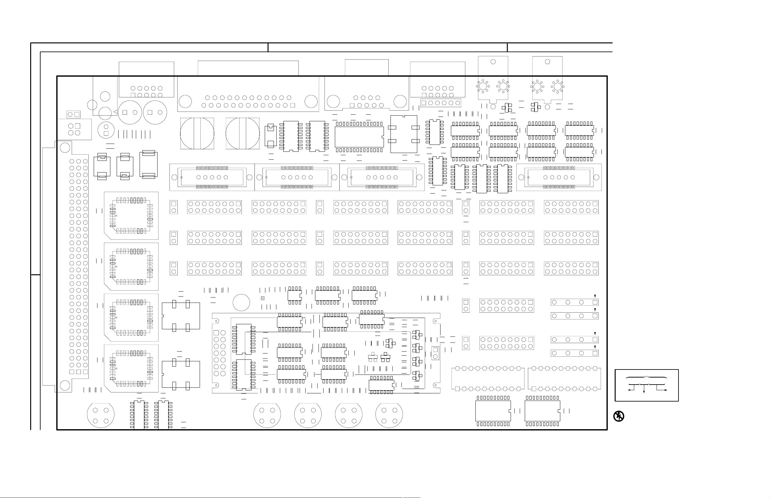
123
A
J110
S110
J111
DS210
C
CR120
C130
R210
C210
CR220
C212
C
U231
R211
F220
C213C211
R212
J330
J340
R501
J500
U511
R513
J630
J640
C610
J620
Y610
R620
R621
J400
R500
J320
C411
L410L310
C421
R410
J420
R510
R511 R512
J430
J440 J740
J540
J541 J531
C600
J730J530
C622
R720
J600J200
C710
U710
C720
U720
R721
R710
R722
J601
R711
U712
U722
R730
R712
R723
R713
J731
J741
R714
R700
R715
C713
C723 C712
U726
J700
CR800
R810
U821U723
U822
J830
J840
R811
C800
C810
C811
C820
CR801
J800
R900
R800
U812U810
C813
C822
U910
U920U824
C911
C921
J820
J930
J940
B
J180
R180
R181
S290
C150
C170 C160
C180
U251
U261
U271
C282
U291
C285
U292
C350
Y360
C370
Y380
R390
J350
J450
R450
R454
R451
U371
R452
R453
R470
R480
C480
R550
TP5
R460
C470
C472
R471
R481
C482
R482
C471
J550
R551
R461
R483
C483
R552
U460
U471
U480
U461
C485
R484
R580
S590
C550
R560
C570 C560
C580
R561
C572
C573
R570
R585
U560
J551
U563
U572
U580
C582
R581
R582
S591
C551
R562
C585
C565
C576
C584
U564
CR670
C586
R583
R584
U661
R670
R671
C671
C670
U681
R672
R673
C650
R660
R661
Q670
CR671
R674
S690S490
R675
C661
R662
C672
R676
R677
R678
R679
R680
C680
R663
Q671
Q672
Q673
Q680
R681
R682
J750
R750
R683
R684
R685
R751
R770
J770
R752
R771
R753
C770
R772
R760
J751J760
J771
U791
J850
J860
J870
C890
U890
J950J650
J960
J961
J970
J971
DS880DS780
C990
G9DĆ2234Ć00
COMPONENT NUMBER EXAMPLE
A23 A2 R1234
ChassisĆmounted components have no Assembly Number
prefixĊsee end of Replaceable Electrical Parts List.
STATIC
SENSITIVE
DEVICES
A01 TLA 7QS Quickstart Training Board (front)
TLA QuickStart Technical Reference Manual
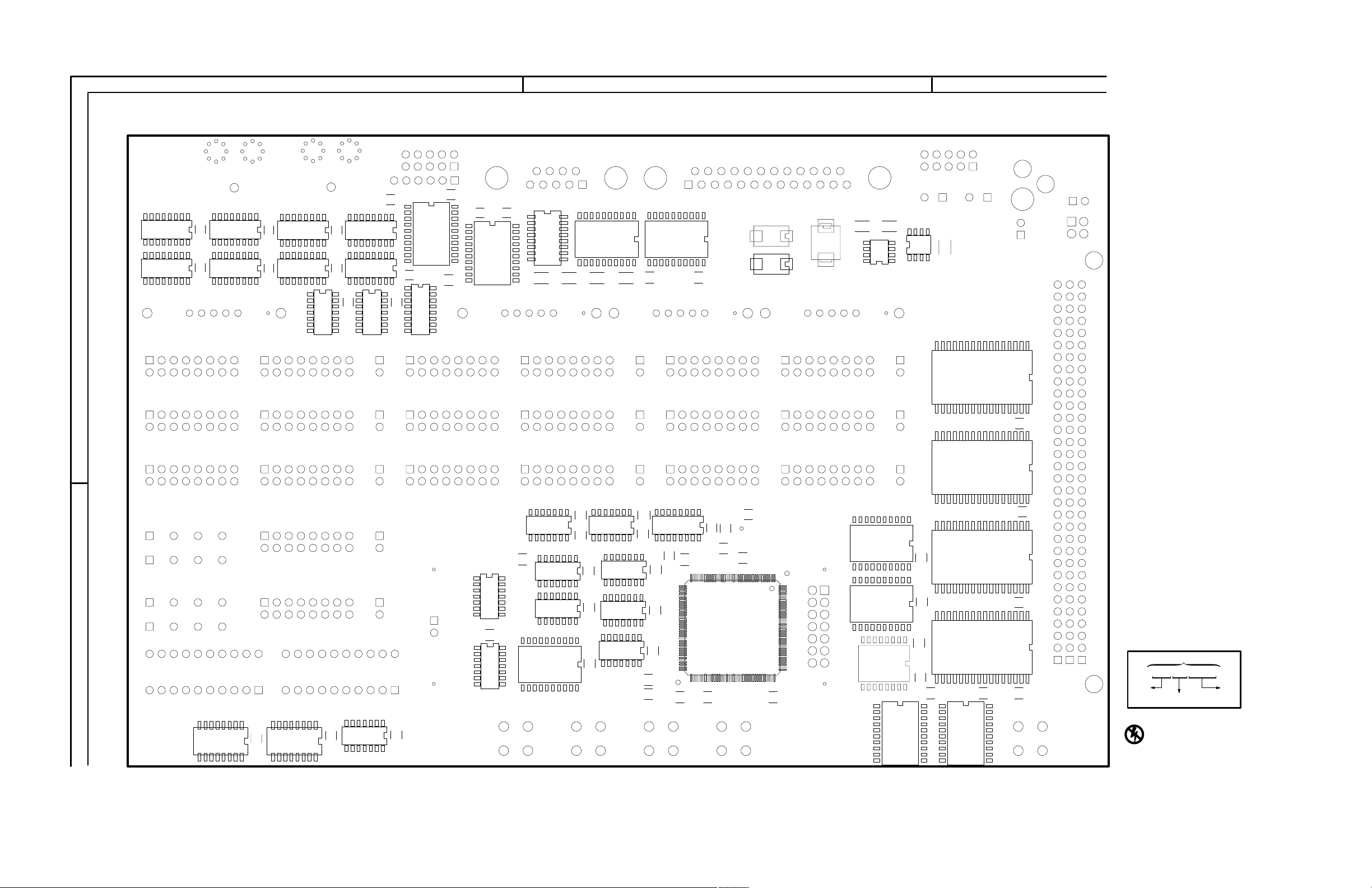
123
A
U0911
U0921
C0910
C0920
U0813
U0825
C0812
C0821
U0811
U0823
U0820
C0714
C0725
C0724
U0713
U0724
C0711
U0725
C0721
C0722
U0711
U0721
C0612
C0621
R0611
U0610
C0611
C0660
C0620
U0660
R0610
U0565
C0564
R0564
C0563
U0510
U0562
C0521C0523 C0522
U0561
C0520
C0562
R0562
U0410
U0462
C0561
C0462
R0463
C0422
C0461
R0462
R0460
R0461
C0460
C0410
C0420
C
CR0310
R0310R0311
Q0310
U0360
U0210
C0260
C0214
U0230
C0240
U0250
C0151
U0260
B
R0890R0891
C0891
TLA QuickStart Technical Reference Manual
C0791
U0790
C0790
C0673
U0670
U0682
U0573
U0680
C0575
C0583
U0570
U0571
C0581
R0580
C0571
C0574
R0581
C0484
U0470
C0481
U0370
U0380
U0390
R0270
C0271
C0284
C0283
U0270
C0281
U0290
C0270
C0280
G9DĆ2234Ć00
COMPONENT NUMBER EXAMPLE
A23 A2 R1234
ChassisĆmounted components have no Assembly Number
prefixĊsee end of Replaceable Electrical Parts List.
STATIC
SENSITIVE
DEVICES
A01 TLA 7QS Quickstart Training board (back)
A01 TLA 7QS Quickstart Training Board Component Locator
CIRCUIT
NUMBER
C0151* B3 30A5
C0214* A3 12C2
C0240* A3 30B5
C0260* B2 30B6
C0270* B3 30C6
C0271* B2 30C5
C0280* B3 30B5
C0281* B3 30B5
C0283* B3 30C6
C0284* B2 30C6
C0410* A2 12C5
C0420* A2 12C5
C0422* A2 30B6
C0460* B2 30B5
C0461* B2 30C5
C0462* B2 30C6
C0481* B2 30A6
C0484* B2 30B5
C0520* A2 30C6
C0521* A2 18A5
C0522* A2 18B4
C0523* A2 18B4
C0561* B2 30C5
C0562* B2 30C6
C0563* B2 30B6
C0564* B2 30A6
C0571* B2 30A5
C0574* B2 30C5
C0575* B2 30C6
C0581* B2 30C6
C0583* B2 30C6
C0611* A1 30D6
C0612* A1 30A6
C0620* A2 18A5
C0621* A1 30A6
C0660* B1 30A5
C0673* B1 30C5
C0711* A1 30A6
C0714* A1 30C5
C0721* A1 30A6
C0722* A1 30B5
C0724* A1 30A5
C0725* A1 30C6
C0790* B1 30D5
C0791* B1 30D5
C0812* A1 30A6
C0821* A1 30C5
C0891* B1 30B6
C0910* A1 30B5
C0920* A1 30A5
C130 A1 30D5
C150 A1 30B6
C160 B1 30D5
C170 B1 30D6
BOARD
LOCATION
SCHEM
LOCATION
CIRCUIT
NUMBER
C180 B1 8C1
C210 A1 12C1
C211 A1 12C2
C212 A1 12C1
C213 A1 12C2
C282 B1 30A6
C285 B1 30B6
C350 B1 30A5
C370 B1 30C5
C411 A1 12C6
C421 A1 30A5
C470 B1 2D2
C471 B1 2D2
C472 B1 2D2
C480 B1 30C6
C482 B1 30C5
C483 B1 8C3
C485 B2 8D3
C550 B2 30A5
C551 B2 30D5
C560 B2 30D6
C565 B2 30C6
C570 B2 30C5
C572 B2 29B1
C573 B2 26A1
C576 B2 30A5
C580 B2 30C5
C582 B2 8C4
C584 B2 30B6
C585 B2 8D4
C586 B2 27B4
C600 A2 30B5
C610 A2 30A5
C622 A2 30A6
C650 B2 30D6
C661 B2 28B3
C670 B2 28D3
C671 B2 30C5
C672 B2 28A3
C680 B2 30B5
C710 A2 30D6
C712 A2 30B6
C713 A2 30C5
C720 A2 30D6
C723 A2 30D6
C770 B2 28A3
C800 A3 30D5
C810 A3 30D6
C811 A3 30D5
C813 A3 30D6
C820 A3 30B6
C822 A3 30C5
C890 B3 30D5
BOARD
LOCATION
SCHEM
LOCATION
CIRCUIT
NUMBER
C911 A3 30B6
C921 A3 30D5
C990 B3 30D6
CR0310* A2 12C4
CR120 A1 12B2
CR220 A1 12B2
CR670 B2 27B4
CR671 B2 27B5
CR800 A3 20A4
CR801 A3 20A4
DS210 A1 12C6
DS780 B2 9C5
DS880 B3 9A5
F220 A1 12B2
FD0191* A1 30C1
FD0901* B3 30C1
FD190 A3 30C2
FD900 B1 30C2
J110 A1 12B1
J111 A1 12A1
J180 A1 11B3
J180 A1 11B4
J180 A1 11B6
J200 A1 20C4
J320 A1 16B3
J330 A1 13C5
J340 A1 15C5
J350 A1 14D5
J400 A1 19A5
J420 A2 17B3
J430 A1 13B5
J440 A1 15C5
J450 A1 14B5
J500 A2 18A6
J530 A1 13A5
J531 A2 13C3
J540 A1 15B5
J541 A2 15C3
J550 A1 14A5
J551 A2 14C2
J600 A2 18C6
J601 A2 20C4
J620 A2 16B5
J630 A2 13B3
J640 A2 15C3
J650 A2 14B2
J700 A2 20A4
J730 A2 13A3
J731 A2 21A1
J740 A2 15B3
J741 A2 21A3
J750 A2 14A2
J751 A2 21A4
BOARD
LOCATION
SCHEM
LOCATION
CIRCUIT
NUMBER
J760 B2 21A5
J770 B2 8B5
J771 B2 21A6
J800 A3 20A4
J820 A3 17B5
J830 A3 21B1
J840 A3 21B3
J850 A3 21A4
J860 B3 21A5
J870 B3 21A6
J930 A3 21A1
J940 A3 21A3
J950 A3 21B4
J960 B3 21C5
J961 B3 21B5
J970 B3 21C6
J971 B3 21B6
L310 A1 12C4
L410 A1 12C5
MH0100* A3 30B2
MH0190* A1 30B1
MH0620* B2 30B1
MH0660* B1 30B2
MH0900* B3 30C1
MH0990* B1 30B3
MH1 B1 30C2
MH2 B2 30C2
Q0310* A2 12C4
Q670 B2 28A2
Q671 B2 28A3
Q672 B2 26C5
Q673 B2 26D5
Q680 B2 27B5
R0270* B2 2B5
R0310* A2 12C4
R0311* A2 12C4
R0460* B2 2B5
R0461* B2 2B5
R0462* B2 2B5
R0463* B2 2A5
R0562* B2 29C5
R0564* B2 29B5
R0580* B2 2A5
R0581* B2 2B5
R0610* A2 19B3
R0611* A1 24A2
R0890* B1 9C6
R0891* B1 9A6
R180 B1 8C1
R181 B1 8C1
R210 A1 12C6
R211 A1 12C3
R212 A1 12C3
BOARD
LOCATION
SCHEM
LOCATION
CIRCUIT
NUMBER
R390 B1 10B3
R410 A2 19C3
R450 B1 2A5
R451 B1 2A5
R452 B1 2A5
R453 B1 2A5
R454 B1 2A5
R460 B1 5D2
R461 B1 5D2
R470 B1 2B1
R471 B1 8B5
R480 B1 2C1
R481 B1 8B5
R482 B1 8C3
R483 B1 8C3
R484 B2 8D3
R500 A2 19A1
R501 A2 19A1
R510 A2 19A3
R511 A2 19A2
R512 A2 19A2
R513 A2 19A1
R550 B1 14B4
R551 B1 2A5
R552 B2 2A5
R560 B2 29B5
R561 B2 29B1
R562 B2 14A5
R570 B2 26A1
R580 B2 8D3
R581 B2 8C4
R582 B2 8C4
R583 B2 8D4
R584 B2 8D4
R585 B2 26A2
R620 A2 25B2
R621 A2 25A4
R660 B2 28B3
R661 B2 28C3
R662 B2 28A2
R663 B2 28C4
R670 B2 28D3
R671 B2 27B4
R672 B2 28A2
R673 B2 27B5
R674 B2 27B5
R675 B2 27B5
R676 B2 28A3
R677 B2 26C4
R678 B2 26D5
R679 B2 27B3
R680 B2 27B3
R681 B2 27C5
BOARD
LOCATION
SCHEM
LOCATION
CIRCUIT
NUMBER
R682 B2 27C4
R683 B2 28A3
R684 B2 26C5
R685 B2 26B4
R700 A2 20A3
R710 A2 25B2
R711 A2 25B2
R712 A2 25C2
R713 A2 25C3
R714 A2 25B3
R715 A2 20A3
R720 A2 25A2
R721 A2 25A2
R722 A2 25A2
R723 A2 25A2
R730 A2 14D1
R750 B2 28C3
R751 B2 28D3
R752 B2 28D3
R753 B2 28C3
R760 B2 14D1
R770 B2 28A3
R771 B2 28A3
R772 B2 28B3
R800 A3 20A3
R810 A2 25B3
R811 A3 25B3
R900 A3 20A3
S110 A1 12A2
S290 B1 8C1
S490 B1 8C2
S590 B2 8D2
S591 B2 8C4
S690 B2 8D4
TP5 B1 14B4
U0210* A2 12C3
U0230* A3 4C4
U0250* A3 4A4
U0260* B3 4C3
U0270* B3 4A3
U0290* B3 7A4
U0360* B2 10C5
U0370* B2 10C5
U0380* B2 10B5
U0390* B2 7C3
U0410* A2 19C2
U0462* B2 6A2
U0470* B2 2A4
U0510* A2 19A2
U0561* B2 5A4
U0561* B2 5B4
U0561* B2 8A3
U0562* B2 5A4
BOARD
LOCATION
SCHEM
LOCATION
CIRCUIT
NUMBER
U0562* B2 5C4
U0562* B2 6C5
U0565* B2 4C1
U0565* B2 6A5
U0565* B2 6B5
U0565* B2 6B5
U0565* B2 6C4
U0565* B2 10C4
U0570* B2 5A2
U0570* B2 5B2
U0570* B2 10C3
U0571* B2 10A2
U0571* B2 10D3
U0571* B2 10D4
U0573* B2 7A6
U0573* B2 7B6
U0573* B2 7C6
U0573* B2 8A3
U0573* B2 8B3
U0573* B2 14A5
U0610* A1 25C2
U0660* B2 5B5
U0670* B1 5A2
U0670* B1 26B5
U0680* B2 7B4
U0682* B1 7A2
U0682* B1 7A3
U0682* B1 7B2
U0682* B1 7B3
U0711* A1 25B5
U0713* A1 23A3
U0721* A1 25A4
U0724* A1 23A4
U0725* A1 25B4
U0725* A1 28B2
U0790* B1 9A2
U0790* B1 9A3
U0790* B1 9B2
U0790* B1 9B3
U0811* A1 23B3
U0813* A1 23C3
U0820* A1 25B4
U0820* A1 25B4
U0820* A1 25B5
U0820* A1 25B5
U0820* A1 25C5
U0823* A1 23B4
U0825* A1 23C4
U0911* A1 23C3
U0921* A1 23C4
U231 A1 3A4
U251 A1 3C4
U261 B1 3A2
BOARD
LOCATION
SCHEM
LOCATION
CIRCUIT
NUMBER
U271 B1 3C2
U291 B1 10B4
U292 B1 10A3
U371 B1 8B5
U460 B2 29B2
U461 B2 2C1
U471 B2 6B5
U471 B2 6C5
U471 B2 6D3
U471 B2 14C1
U480 B2 26C3
U511 A2 18A4
U560 B2 29B5
U563 B2 29B4
U563 B2 29C4
U564 B2 14A5
U564 B2 15A4
U572 B2 24B1
U572 B2 24C1
U572 B2 26A1
U572 B2 26C2
U572 B2 29B1
U580 B2 26C4
U580 B2 26D4
U580 B2 28C2
U661 B2 5A1
U661 B2 24B2
U661 B2 28B3
U661 B2 28D4
U681 B2 27A3
U681 B2 29C2
U710 A2 24A4
U710 A2 24A5
U710 A2 24B5
U712 A2 22A3
U720 A2 24D2
U722 A2 24B2
U722 A2 25B4
U722 A2 25C4
U723 A2 22A4
U726 A2 25A3
U791 B2 9B4
U810 A2 22B3
U812 A3 22C3
U821 A2 22B4
U822 A2 24C5
U824 A3 22C4
U890 B3 9A4
U910 A3 22C3
U920 A3 22C4
Y360 B1 2D4
Y380 B1 2D3
Y610 A2 24A1
BOARD
LOCATION
SCHEM
LOCATION
*Asterisks indicate components located on the back of the board.
A01 TLA 7QS Quickstart Training board component locator
TLA QuickStart Technical Reference Manual

MICROCONTROLLER.PROCESSORTLA 7QS
 Loading...