

Page 1

PCI-936
PENTIUM PROCESSOR PCI-ISA SBC
Technical Rererence Manual
Version2.3 (Jul 2002)
The latest releases of the Technical Reference Manuals are available at
ftp://ftp.kontron.ca/support/Product_Manuals/
Ref. : M6004_TECH
www.kontron.com
Page 2

FOREWORD
The information in this document is provided for reference purposes only. Kontron does not
assume any liability for the application of information or the use of products described
herein.
This document may contain information or refer to products protected by the copyrights or
patents of others and does not convey any license under the patent rights of Kontron, nor the
rights of others.
Printed in Canada.
Copyright 2001 by Kontron Inc, Boisbriand, Qc J7G 2A7
Page 3
READ ME FIRST
WARNINGS
Take heed of these warnings that concern the PCI-936:
Installing a Processor
Careful attention should be taken when installing a processor:
Faulty jumper settings may definitely damage your processor.
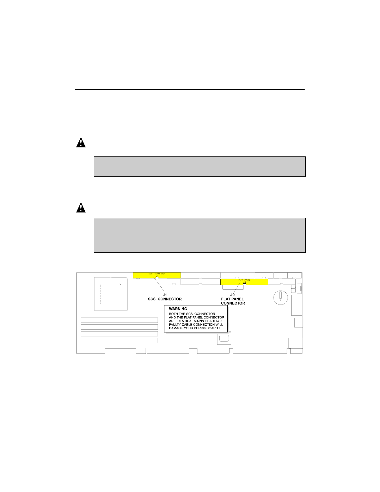
SCSI & Flat Panel 50-Pin Connectors
Careful attention should be taken when connecting SCSI or Flat Panel cables to the
PCI-936 board, since both the J1 SCSI connector and the J9 Flat Panel connector
are 50-pin headers.
Faulty connections will damage the PCI-936 board!
Page 4

PCI-936 Technical Reference Manual
Adapter cables
When connecting Serial Ports, the use of Taiwanese adapter cables is not
recommended, since the pinout is often incorrect. The direct crimp design offered by
KONTRON allows the simplest cable assembly. All these cables are available from
KONTRON by contacting the Sales department.
Page 5

IMPORTANT INFORMATION
Before operating your Single Board Computer, please note the following:
Powering up the system
If you should encounter a problem, verify the following items:
• Make sure that all connectors are connected properly. On the standard flat ribbon
cable used for the floppy connector, pin 1 is indicated by small red stripe. Verify
that this red stripe is located on the appropriate side of the connector.
• Verify your boot diskette. It must be a system disk and it must be in proper
working order.
• If the system still does not start up properly, you should try booting your system
with only the power cord and video monitor connected to the board (this is the
minimum required to see if the board is working).
• If the system still does not start up please refer to Emergency Procedure Section
F in the Appendices.
• If you still are not able to get your board up and running, contact our Technical
Support department for assistance.
Battery Configuration
Your computer board is equipped with a standard non-rechargeable lithium battery.
To preserve the useful life of the battery, the jumper that enables the battery is
not installed when you receive the board. If you need a jumper cap, we suggest
you use the one on the Watchdog Timer jumper since it is rarely needed; if you wish
to purchase jumper caps, you can contact KONTRON’s Sales department to order
them.
Exercise Caution while Replacing Lithium Battery
Danger of explosion if battery is incorrectly replaced.
Replace only with the same or equivalent type recommended by the manufacturer.
Dispose of used batteries according to the manufacturer's instructions.
III
Page 6

PCI-936 Technical Reference Manual
CHANGES BETWEEN REVISIONS OF THE BOARD
✏✏✏✏
Preventing Viruses
RON takes every precaution against computer viruses. For your
KONT
protection, we have safety sealed all utility diskettes. If the seal is broken, do not use
the diskette. Destroy the diskette immediately and contact our Technical Support
department for further instructions at (514) 437-5682 (Canada) or at +49 811 / 600
15-0 (Germany).
To safeguard against computer viruses in general, do not freely lend your utility
diskettes and regularly perform virus scans on all your computer systems.
Changes Between Revision 1 And Revision 0
• USB Connector (J7) pinout modified to meet “Industry Standard”.
• Feature Connector (J11) replaced by VPORT.
• Thermal Management is supported
• Support of external 8-bit VPORT via 26-pin male header (J11).
• Support 3.3-Volt and 5-Volt Flat Panel.
• Standard 4-pin PS/2 mouse header (J25) added.
• Jumper W24 (Voltage Level Selection for Flat Panel) added.
• Jumper W1 (First-Level Cache Write-Back Write-Through Selection) removed.
✏✏✏✏
Changes Between Revision 2 And Revision 1
• Rev. 2 boards support Pentium MMX 166/200/233 and K6 166/200 processors
Page 7

TABLE OF CONTENTS
PART 1
1. PRODUCT OVERVIEW....................................................................... 1-1
2. FEATURES.......................................................................................... 2-1
3. COMPATIBILITY WITH KONT
RON PRODUCTS ................................. 3-1
PART 2
4. STATIC ELECTRICITY PRECAUTIONS ............................................ 3-1
5. UNPACKING....................................................................................... 5-1
6. INSTALLING & WORKING WITH SYSTEM COMPONENTS............ 6-1
6.1. INSTALLING SYSTEM MEMORY ...................................................................................6-1
6.1.1 72-PIN SIMM CONFIGURATION AND LOCATION.................................................. 6-1
6.1.2 SIMM INSTALLATION..............................................................................................6-2
6.2. INSTALLING MICROPROCESSOR & FAN.....................................................................6-4
6.2.1 INSTALLING MICROPROCESSOR .........................................................................6-4
6.2.2 FAN CONNECTOR ..................................................................................................6-5
6.3. ENABLING CACHE MEMORY ........................................................................................6-5
6.4. SELECTING BIOS BOOT OPTIONS...............................................................................6-6
6.5. INSTALLING SUPERVISOR UTILITIES ..........................................................................6-6
6.5.1 SUPERVISOR I/O REGISTERS...............................................................................6-6
6.5.2 POWER FAIL DETECTION......................................................................................6-7
6.5.3 WATCHDOG DETECTION.......................................................................................6-8
6.5.4 WATCHDOG TIMERS..............................................................................................6-8
6.5.5 SYSTEM RESET HISTORY STATUS.................................................................... 6-10
6.6. INSTALLING PCI-936 IN PASSIVE BACKPLANE......................................................... 6-10
6.7. CONNECTING INTERFACE DEVICES (KEYBOARD, SPEAKER, RESET, LED)... 6-11
6.8. CONNECTING A MONITOR..........................................................................................6-12
6.9. CONNECTING A MOUSE .............................................................................................6-12
I
Page 8

PCI-936 Technical Reference Manual
7. INSTALLING STORAGE DEVICES.................................................... 7-1
7.1. CONNECTING A FLOPPY DRIVE...................................................................................7-1
7.1.1 FLOPPY SOFTWARE SETUP ................................................................................. 7-2
7.1.2 FLOPPY CONNECTOR PINOUT.............................................................................7-2
7.2. ENHANCED IDE DEVICES ............................................................................................. 7-3
7.2.1 ENHANCED IDE CONNECTORS LOCATION & HOOK-UP.....................................7-3
7.3. SCSI DEVICES................................................................................................................7-4
7.3.1 INSTALLING A FIXED SCSI HARD DISK ................................................................ 7-4
7.3.2 INSTALLING OTHER SCSI DEVICES .....................................................................7-5
8. INSTALLING VIDEO ........................................................................... 8-1
8.1. VIDEO CONTROLLER ....................................................................................................8-1
8.1.1 INSTALLING VIDEO DRIVERS................................................................................8-1
8.1.2 DISABLING VIDEO CONTROLLER.........................................................................8-1
8.2. INSTALLING CRT VIDEO DISPLAY................................................................................8-1
8.2.1 CONNECTING CRT VIDEO DISPLAY ..................................................................... 8-1
8.2.2 VPORT.....................................................................................................................8-1
8.3. FLAT PANEL ...................................................................................................................8-2
8.3.1 FLAT PANEL CONNECTOR PINOUT......................................................................8-2
8.3.2 FLAT PANEL INSTALLATION..................................................................................8-2
9. INSTALLING PERIPHERALS............................................................. 9-1
9.1. SERIAL PORTS...............................................................................................................9-1
9.1.1 Serial Port 1 (J5) RS-232..........................................................................................9-2
9.1.2 Serial Port 2 (J6) ......................................................................................................9-3
9.2. USB PORT (C
9.3. PARALLEL PORT............................................................................................................9-7
ONNECTOR - J7) .........................................................................................9-6
10. INSTALLING ETHERNET.......................................................... 10-1
10.1. SETTING UP ETHERNET.............................................................................................10-1
10.1.1 CABLING ...............................................................................................................10-1
10.1.2 CONFIGURATION .................................................................................................10-1
10.2. ETHERNET CONNECTORS .........................................................................................10-2
10.3. ETHERNET LED
S STATUS........................................................................................... 10-2
II
Page 9

PART 3
11. CONFIGURING DMA & IRQ...................................................... 10-1
11.1. ALLOCATING DMA CHANNELS...................................................................................11-1
11.2. ALLOCATING IRQ LINES..............................................................................................11-2
12. SETTING JUMPERS.................................................................. 12-1
12.1. CONNECTING THE BATTERY .....................................................................................12-1
12.2. JUMPER SETTINGS ..................................................................................................... 12-1
13. POWERING UP THE SYSTEM.................................................. 13-1
13.1. CONNECTING POW ER SUPPLY (J14) .................................................................................13-1
13.2. P
OWERING UP.................................................................................................................13-1
13.3. T
ROUBLESHOOTING .........................................................................................................13-2
14. SOFTWARE SETUP .................................................................. 14-1
14.1. THE AWARD SETUP PROGRAM.................................................................................14-1
14.1.1 ACCESSING THE AWARD SETUP PROGRAM....................................................14-1
14.1.2 USING AWARD SETUP......................................................................................... 14-3
14.1.3 SAVING CONFIGURATIONS & EXITING AWARD SETUP ................................... 14-5
14.1.4 STANDARD CMOS SETUP ................................................................................... 14-6
14.1.5 BIOS FEATURES SETUP...................................................................................... 14-7
14.1.6 CHIPSET FEATURES SETUP...............................................................................14-9
14.1.7 POWER MANAGEMENT SETUP ........................................................................14-11
14.1.8 PnP/PCI SETUP...................................................................................................14-13
14.1.9 INTEGRATED PERIPHERALS SETUP................................................................ 14-15
14.2. THE VIP-UP PROGRAM ............................................................................................. 14-17
14.2.1 ACCESSING THE VIP-UP PROGRAM ................................................................ 14-17
14.2.2 VIP-UP SCREEN .................................................................................................14-18
III
Page 10

PCI-936 Technical Reference Manual
PART 4
15. VFLASH SOFTWARE................................................................ 14-1
15.1. INTRODUCTION ........................................................................................................... 15-1
15.1.1 VFLASH SOFTWARE OVERVIEW........................................................................ 15-2
15.1.2 TYPES OF FLASH EPROM DISKS .......................................................................15-3
15.1.3 VFLASH REQUIREMENTS....................................................................................15-4
15.2. RUNNING VFLASH.......................................................................................................15-5
15.3. OUTPUT SELECTION...................................................................................................15-6
15.4. FILE SELECTION.......................................................................................................... 15-8
15.4.1 MENU COMMANDS.............................................................................................15-10
15.4.2 LIST OF SELECTED FILES................................................................................. 15-12
15.4.3 DUPLICATE FILES MENU................................................................................... 15-13
15.5. FILE TRANSFER......................................................................................................... 15-14
15.5.1 TRANSFER STATUS OF ONBOARD FLASH PROGRAMMING SCREEN..........15-14
15.5.2 TRANSFER STATUS OF EXTERNAL FLASH PROGRAMMING SCREEN......... 15-15
15.6. BATCH MODE............................................................................................................. 15-17
15.6.1 BATCH MODE COMMAND LINE PARAMETERS................................................15-18
15.6.2 BATCH MODE COMMAND LINE OPTIONS ........................................................ 15-19
15.6.3 BATCH MODE ERROR CODES ..........................................................................15-21
16. FLASH FILE SYSTEM II ........................................................... 16-1
16.1. INTRODUCTION ........................................................................................................... 16-1
16.2. SETTING UP CONFIG.SYS FOR FLASH FILE SYSTEM II...........................................16-2
16.3. CREATING & FORMATTING AN MS-FLASH PARTITION............................................16-3
16.3.1 USING MEMCARD MENU OPTIONS ....................................................................16-4
16.3.2 USING MEMCARD DIRECTLY FROM THE COMMAND PROMPT ....................... 16-6
17. UPDATING BIOS WITH UBIOS ................................................ 17-1
17.1. INTRODUCTION ........................................................................................................... 17-1
17.2. UBIOS - INTERACTIVE MODE .....................................................................................17-2
17.2.1 MAIN MENU........................................................................................................... 17-3
17.2.2 UPDATE MENU .....................................................................................................17-4
17.2.3 FLASH BIOS COPY MENU....................................................................................17-6
17.3. UBIOS - BATCH MODE................................................................................................. 17-7
18. VT100 MODE ............................................................................. 18-1
18.1. VT100 REQUIREMENTS...............................................................................................18-1
18.2. VT100 SETUP & CONFIGURATION .............................................................................18-1
18.3. RUNNING WITHOUT A TERMINAL ..............................................................................18-3
19. DOWNLOAD MODE .................................................................. 19-1
IV
Page 11

PART 5
A. BOARD SPECIFICATIONS..........................................................A-1
A.1 ELECTRICAL ..........................................................................................................A-1
A.2 M
A.3 E
A.4 R
B. MEMORY & I/O MAPS................................................................ B-1
C. BOARD DIAGRAMS ................................................................... C-1
C.1 C-1 BLOCK DIAGRAM.............................................................................................C-1
D. CONNECTOR LOCATIONS & PINOUTS.................................... D-1
D.1 LOCATION OF CONNECTORS ON THE BOARD .............................................................D-1
D.2 C
ECHANICAL......................................................................................................... A-1
NVIRONMENTAL ...................................................................................................A-2
ELIABILITY...........................................................................................................A-2
ONNECTOR PINOUTS ...........................................................................................D-5
D.2.1 PCI Ultra SCSI Interface Connector (J1) - Pinout .................................................... D-5
D.2.2 Enhanced IDE Connectors (J2 and J8) - Pinout ...................................................... D-6
D.2.3 Floppy Disk Connector (J3) - Pinout ........................................................................ D-7
D.2.4 Multi-Function Connector - (J4) - Pinout ................................................................. D-7
D.2.5 Serial Port 1 - (J5) RS-232 - Pinout ......................................................................... D-8
D.2.6 Serial Port 2 - (J6) RS-232 - Pinout ......................................................................... D-8
D.2.7 Serial Port 2 - (J6) RS-422/RS-485 - Pinout ............................................................D-8
D.2.8 USB Connector (J7) - Pinout ................................................................................... D-9
D.2.9 Flat Panel Connector (J9) - Pinout........................................................................... D-9
D.2.10 Parallel Port Connector (J10) - Standard Mode ..................................................... D-10
D.2.11 Parallel Port Connector (J10) - EPP Mode ............................................................ D-10
D.2.12 Parallel Port Connector (J10) - ECP Mode ............................................................ D-11
D.2.13 VPORT Connector (J11) - Pinout .......................................................................... D-12
D.2.14 External Battery Connector (J12) - Pinout ............................................................. D-12
D.2.15 Emergency BIOS Boot (J13) - Pinout .................................................................... D-12
D.2.16 External Power Connector (J14) - Pinout............................................................... D-13
D.2.17 VGA Connector (J15) - Pinout ............................................................................... D-13
D.2.18 PS/2 Mouse Connector (J16) Din .......................................................................... D-13
D.2.19 Fan Connector (J17) - Pinout................................................................................. D-14
D.2.20 Ethernet 10/100 Base-Tx RJ-45 Connector (J18) - Pinout ..................................... D-14
D.2.21 PS/2 Mouse Connector (J25) - Pinout ................................................................... D-14
D.2.22 PCI Bus Connector A1-A30 and B1-B30 (J19 and J22) ......................................... D-15
D.2.23 PCI Bus Connector A31-E62 and B31-F62 (J19 and J22) ..................................... D-16
D.2.24 ISA Bus Connector C and D (J20 and J23) - Pinout .............................................. D-17
D.2.25 ISA Bus Connector A and B (J21 and J24) - Pinout............................................... D-18
V
Page 12

E. BIOS SETUP ERROR CODES.....................................................E-1
E.1 POST BEEP ......................................................................................................... E-1
E.2 POST M
E.3 E
E.4 POST C
ESSAGES.................................................................................................E-1
RROR MESSAGES ................................................................................................ E-2
ODES ...................................................................................................... E-5
F. EMERGENCY PROCEDURE .......................................................F-1
F.1 SYMPTOMS ........................................................................................................... F-1
F.2 E
F.3 G
MERGENCY PROCEDURE ......................................................................................F-1
ENERATE AN EMERGENCY FLOPPY DISKETTE......................................................... F-2
G. LIST OF APPROVED VENDORS................................................ G-1
G.1 DRAM (FOUR 72-PIN SOCKETS LOCATED AT U22, U27, U31 AND U36).................. G-1
G.2 I
NTERFACE CONNECTORS ..................................................................................... G-2
VI
Page 13

PRODUCT DESCRIPTION
PAR
T
1. PRODUCT OVERVIEW
2. FEATURES
3. COMPATIBILITY WITH KONTRON PRODUCTS
1
Page 14

Page 15

1. PRODUCT OVERVIEW
The PCI-936 is a Pentium / K6 (Intel / AMD) PCI and PC/AT compliant industrial Single
Board Computer (SBC) based on the full size PC/AT card with onboard video capabilities.
The board may be installed into a standard passive ISA backplane, or into a PCI Industrial
Computer Manufacturers Group (PICMG) passive PCI-ISA backplane.
The SBC and backplane assembly is used as a substitute for the standard PC motherboard, and
in general includes all of the standard interfaces and peripherals that are normally included in a
top of the line PC.
This compact solution allows an industrial user the possibility of designing a system that uses
standard x86 software and peripherals, but in an industrial environment where reliability,
integration and service are of major concern.
The PCI-936 uses Intel 430 HX (Triton II) chipset. This chipset is fully compliant with the
PCI Local Bus Specification, Revision 2.1, and is implemented with a north & south bridge
architecture. A full implementation of the PCI revision 2.1 specification allows the PCI-936 to
efficiently use the PCI bus.
1-1
Page 16

Page 17

2. FEATURES
The PCI-936 includes the following features:
§ Microprocessor supported (maximum internal CPU clock speed):
- Intel Pentium: 100, 120, 133, 150, 166 and 200MHz
- Intel Pentium MMX: 166, 200 and 233MHz
- AMD K6: 166 and 200MHz
§ Cache: The PCI-936’s cache is implemented with synchronous SRAM. This feature
enhances the operation of the circuit by eliminating wait states on cache accesses. Cache
size options include 256KB and 512KB.
§ Intel Triton II Chipset:
- Flexible CPU interface including full write-back internal and external cache operation.
- Concurrent CPU/cache and PCI/DRAM operation.
- Synchronous Pipelined Burst SRAM cache.
- EDO as well as Fast Page Mode DRAM access.
- Parity or ECC support.
- Full functional compliance of the PCI interface.
- Enhanced IDE support.
- Plug and Play compatibility.
- Power management.
- Supervisor Utilities.
- USB Support
§ Video: The PCI-936 is implemented with advanced video functions including the C&T
65550 video chip from the Chips & Tech family. It offers significant improvements over
previous generation devices. Its features are:
- 64-bit graphics engine.
- Video playback acceleration.
- 24-bit color video DAC.
- Hardware Windows acceleration.
- 32-bit PCI host interface.
- Supports non-interlaced CRT resolutions up to 1280 x 1024 pixels (256 colors).
Compatible with CGA, EGA, Hercules, MDA, VGA, SVGA, XGA, and SXGA.
- Supports Flat Panel resolutions up to 1024x768x64K Colors.
- Simultaneous CRT/Flat Panel Capability.
- Supports video memories up to 2MB.
- VPORT (Asynchronous Digital Video) support.
2-1
Page 18

PCI-936 Technical Reference Manual
§ System Memory:
- Four vertical 72-pin SIMM sockets support DRAM memory configurations from 8 to
512 MB.
- Uses standard 5V, 70ns/60ns single-sided or double-sided 72-pin SIMMs.
- Supports 1Mx36, 2Mx36, 4Mx36, 8Mx36, 16Mx32, 32Mx32 modules.
§ Flash Disk: includes a bootable Flash Disk device with capacities of 2 or 4 MB.
§ Bus Support:
- ISA Bus (IEEE P966 Specification). High-drive buffers let the PCI-936 drive up to 20
slots.
- PCI Local Bus Specification, Revision 2.1.
§ PICMG interface: This includes an interface to the ISA bus and the PCI bus. The PCI-
936 can support memory data streaming up to 112MB/s. The PCI-936 provides
concurrent PCI master and CPU/DRAM operations. It also implements “delayed
transaction” to increase the availability of the PCI bus.
§ Enhanced IDE interface: Enhance IDE controller can drive up to four IDE devices with
transfer rates up to 22MB/s. The PCI-936 includes two separate IDE data bus and control
signals.
§ SCSI interface: This interface is implemented with a PCI Ultra SCSI controller. The
circuit uses a Symbios 53C860 controller to perform this function.
§ Ethernet: 100Base-Tx or 10 Base-T interface is implemented with Intel’s 82557 Ethernet
Controller. The IC resides on the PCI bus, which allows very high transfer rates to and
from DRAM.
§ Operating Systems: Runs all operating systems developed for x86 processors: DOS,
Windows 3.1, OS/2, Windows 95, Windows NT, UNIX, QNX and NOVELL 4.10, etc.
§ BIOS and license: Award CPU BIOS, Chips & Tech Video BIOS, Symbios SCSI BIOS.
2-2
Page 19

3. COMPATIBILITY WITH KONTRON PRODUCTS
The PCI-936 is a direct spin-off of the VIPer820 and T1000 products and is Kontron’s
answer to Triton II customer requests.
The board supports processor speeds of up to 233MHz. The major difference between the
PCI-936 and previous full size PCI boards is the Triton II chipset, the 100 Base-Tx Ethernet
and the USB Support.
The PCI-936 meets these specifications while using the same form factor as the PCI-933 (i.e.,
PC/AT and PICMG), except for flat panel interface, which is compatible with that of PCI-
932. The assembly includes an onboard switching regulator to provide power to the Pentium
CPU, which results in a more efficient use of power.
This SBC is designed to plug into a standard passive ISA backplane, or into an industry
standard PICMG passive backplane.
3-1
Page 20

Page 21

CONNECTING AND INSTALLING
PAR
T
4. STATIC ELECTRICITY PRECAUTIONS
5. UNPACKING
6. INSTALLING AND WORKING WITH SYSTEM
COMPONENTS
7. INSTALLING STORAGE DEVICES
8. INSTALLING VIDEO
9. INSTALLING PERIPHERALS
10. INSTALLING ETHERNET
2
Page 22

Page 23

4. STATIC ELECTRICITY PRECAUTIONS
Since static electricity can damage a board, the following precautions should be taken
whenever you handle the PCI-936:
• Keep the board in its antistatic package, until you are ready to install it.
• Touch a grounded surface before removing the board from its package or wear a
grounding wrist strap; this will discharge any static electricity that may have built up on
your body.
• Handle the board by the edges.
4-1
Page 24

Page 25

5. UNPACKING
Follow these recommendations while unpacking:
ù Observe the Static Electricity Precautions (Section 4).
ù After opening the box, save it and the packing material for possible future shipment.
ù Remove the board from its antistatic wrapping and place it on a grounded surface.
• Inspect the board for damage. If there is any damage, or items are missing, notify
Kontron immediately
5-1
Page 26

Page 27
6. INSTALLING & WORKING WITH SYSTEM COMPONENTS
6.1. INSTALLING SYSTEM MEMORY
6.1.1 72-PIN SIMM CONFIGURATION AND LOCATION
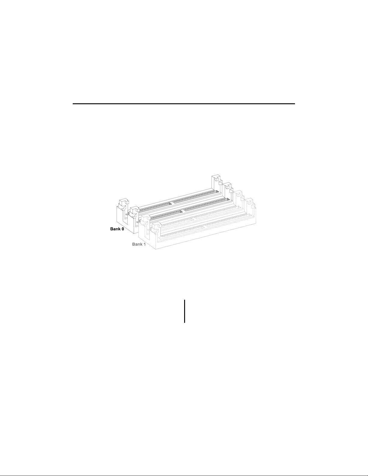
The memory sockets consist of four 72-pin vertical SIMM (Single In-line Memory Module)
sockets divided into two banks labeled: Bank 0 (U22 and U27) and Bank 1 (U31 and U36).
At least 8 MB of system memory (2 SIMMs or 4) must be installed on the PCI-936 for proper
operation. Memory can be configured from 8 MB to 512 MB on the PCI-936 board using 32bit or 36-bit SIMM devices.
Each of the 72-pin vertical SIMM sockets on the board can accept the following 32-bit or
36-bit modules:
1M x 32-bit / 36-bit = 4MB module 8M x 32-bit / 36-bit = 32MB module
2M x 32-bit / 36-bit = 8MB module 16M x 32-bit / 36-bit = 64MB module
4M x 32-bit / 36-bit = 16MB module 32M x 32-bit / 36-bit = 128MB module
The memory banks can be populated separately or jointly. Each must be installed with the
same SIMMs capacity; however, SIMMs capacity used in one bank may be of a different
capacity from the other.
6-1
Page 28
PCI-936 Technical Reference Manual
DRAM devices with parity bit and page mode at 70ns maximum access time are
recommended. Consult Table 6-1 to see examples of recommended DRAM devices on the
PCI-936. Many other models are available and function equally well. Users are encouraged to
check with their local distributors for comparable substitutes.
TABLE 6-1: Recommended DRAM Devices
DRAM Vendor Part Number DRAM Vendor Part Number
1M*36 MICRON MT9D136M-7 16M*32 UNIGEN UG232E3244HKG-6
2M*36 HITACHI HB56D236B2-7C SAMSUNG KMM5364100-7
NEC MC-4210000A36B-70
SAMSUNG KMM5361000B-7 4M*36 HYUNDAI HYM536410AM-70
TI TM124MBK36R-70 MITSUBISHI MH4M36ANXJ-7
TOSHIBA THM361020AS-70 NEC MC-424000A36BH-70
NEC MC-424000A36BJ-70
HITACHI HB56D236BS-7BC TOSHIBA THM3640205-70
HITACHI HB56D236BW-7B
HITACHI HB56D236BW-7C 8M*36 HITACHI HB56D836BR-70A
HYUNDAI HYM536220W-70 TOSHIBA THM368020S-70
MICRON MT18D236M-7 TOSHIBA THM368020SG-70
NEC MC422000A36B-70
SAMSUNG KMM5362000B-7
TOSHIBA THM362040AS-60 32M*32 UNIGEN UG216E3264HKG-6
TOSHIBA THM362040AS-70
6.1.2 SIMM INSTALLATION
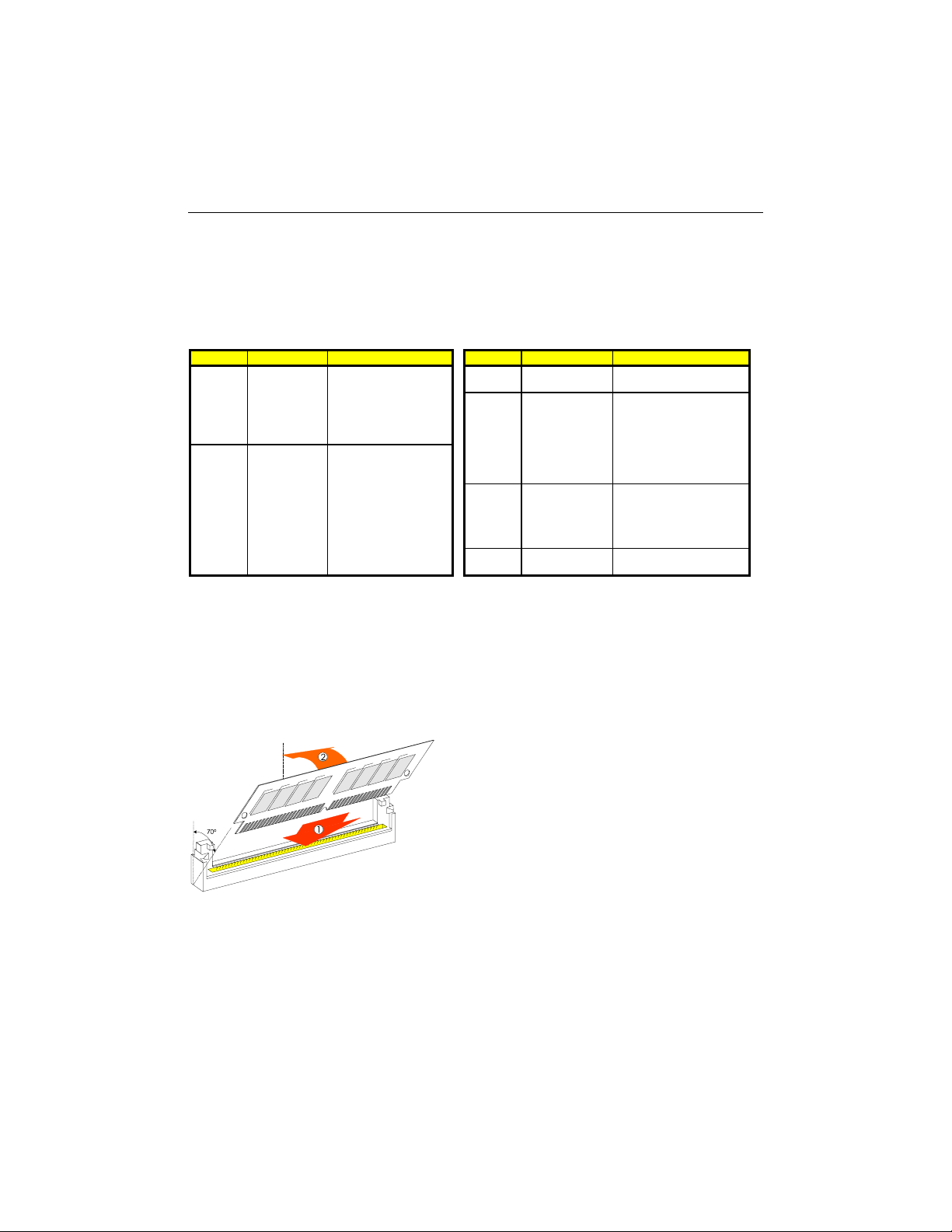
To install the SIMMs in the sockets, proceed as follows:
• With the board flat on the table, turn it so that the
sockets are at the end of the board closest to you.
• Hold the module with the notch on the bottom right
facing you, and insert the connector into the socket at
a 70° angle from the board. Always start inserting the
module in the socket nearest the center of the board.
Then work your way by inserting the other modules,
one by one, towards the exterior edge of the board.
• Snap the module to a vertical position in the socket.
The module is fully inserted when the retaining pegs
snap into the holes at each end of the module.
To remove the SIMMs from the sockets, pull on the retaining pegs located on each side of the
SIMM socket. Once the module has snapped out of the socket, pull gently on it.
6-2
Page 29

Installing and Working with System Components
The following table describes which SIMM configurations may be implemented on the board,
using 72-pin vertical SIMMs:
TABLE 6-2: PCI-936 SIMM Configurations: 8MB - 256MB
SYSTEM U31 U36 U22 U27
MEMORY BANK 1 BANK 0
8MB 4MB (1Mx36) 4MB (1Mx36) -- --
8MB -- -- 4MB (1Mx36) 4MB (1Mx36)
16MB 4MB (1Mx36) 4MB (1Mx36) 4MB (1Mx36) 4MB (1Mx36)
16MB 8MB (2Mx36) 8MB (2Mx36) -- -16MB -- -- 8MB (2Mx36) 8MB (2Mx36)
24MB 8MB (2Mx36) 8MB (2Mx36) 4MB (1Mx36) 4MB (1Mx36)
24MB 4MB (1Mx36) 4MB (1Mx36) 8MB (2Mx36) 8MB (2Mx36)
32MB 8MB (2Mx36) 8MB (2Mx36) 8MB (2Mx36) 8MB (2Mx36)
32MB 16MB (4Mx36) 16MB (4Mx36) -- -32MB -- -- 16MB (4Mx36) 16MB (4Mx36)
40MB 16MB (4Mx36) 16MB (4Mx36) 4MB (1Mx36) 4MB (1Mx36)
40MB 4MB (1Mx36) 4MB (1Mx36) 16MB (4Mx36) 16MB (4Mx36)
48MB 16MB (4Mx36) 16MB (4Mx36) 8MB (2Mx36) 8MB (2Mx36)
48MB 8MB (2Mx36) 8MB (2Mx36) 16MB (4Mx36) 16MB (4Mx36)
64MB 16MB (4Mx36) 16MB (4Mx36) 16MB (4Mx36) 16MB (4Mx36)
64MB 32MB (8Mx36) 32MB (8Mx36) -- -64MB -- -- 32MB (8Mx36) 32MB (8Mx36)
72MB 32MB (8Mx36) 32MB (8Mx36) 4MB (1Mx36) 4MB (1Mx36)
72MB 4MB (1Mx36) 4MB (1Mx36) 32MB (8Mx36) 32MB (8Mx36)
80MB 32MB (8Mx36) 32MB (8Mx36) 8MB (2Mx36) 8MB (2Mx36)
80MB 8MB (2Mx36) 8MB (2Mx36) 32MB (8Mx36) 32MB (8Mx36)
96MB 32MB (8Mx36) 32MB (8Mx36) 16MB (4Mx36) 16MB (4Mx36)
96MB 16MB (4Mx36) 16MB (4Mx36) 32MB (8Mx36) 32MB (8Mx36)
128MB 32MB (8Mx36) 32MB (8Mx36) 32MB (8Mx36) 32MB (8Mx36)
128MB 64MB (16Mx36) 64MB (16Mx36) -- -128MB -- -- 64MB (16Mx36) 64MB (16Mx36)
136MB 64MB (16Mx36) 64MB (16Mx36) 4MB (1Mx36) 4MB (1Mx36)
136MB 4MB (1Mx36) 4MB (1Mx36) 64MB (16Mx36) 64MB (16Mx36)
144MB 64MB (16Mx36) 64MB (16Mx36) 8MB (2Mx36) 8MB (2Mx36)
144MB 8MB (2Mx36) 8MB (2Mx36) 64MB (16Mx36) 64MB (16Mx36)
160MB 64MB (16Mx36) 64MB (16Mx36) 16MB (4Mx36) 16MB (4Mx36)
160MB 16MB (4Mx36) 16MB (4Mx36) 64MB (16Mx36) 64MB (16Mx36)
192MB 64MB (16Mx36) 64MB (16Mx36) 32MB (8Mx36) 32MB (8Mx36)
192MB 32MB (8Mx36) 32MB (8Mx36) 64MB (16Mx36) 64MB (16Mx36)
256MB 64MB (16Mx36) 64MB (16Mx36) 64MB (16Mx36) 64MB (16Mx36)
256MB 128MB (16Mx36) 128MB (16Mx36) -- -256MB -- -- 128MB (16Mx36) 128MB (16Mx36)
512MB 128MB (16Mx36) 128MB (16Mx36) 128MB (16Mx36) 128MB (16Mx36)
36-bit modules are shown, however 32-bit modules are supported.
6-3
Page 30
PCI-936 Technical Reference Manual
6.2. INSTALLING MICROPROCESSOR & FAN
Normally, your PCI-936 will be installed with one of the available Pentium, Pentium MMX or
K6 processors and its cooling fan. However, it may be necessary to reinstall or reconfigure
your board.
6.2.1 INSTALLING MICROPROCESSOR
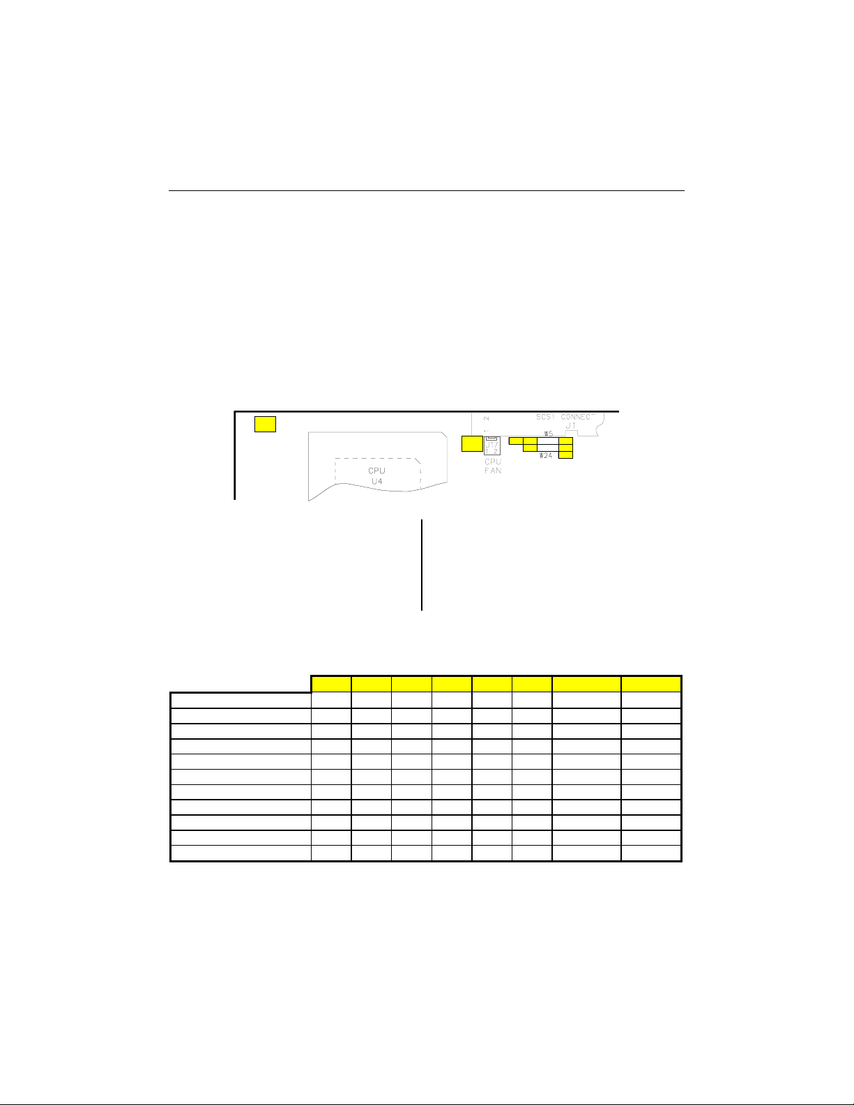
The location of the microprocessor and related jumpers are shown as follows:
W21
W4 and W9
Select the desired multiplier for the internal
CPU clock speed: 1.5x, 2x, 2.5x, 3x or 3.5x
W21
Selects the CPU type - Single supply or
Split plane CPU.
W23
W3, W6, W10 and W11
Select the desired external CPU clock (Bus)
speed: 50MHz, 60MHz or 66Mhz
W23
Selects the CPU core voltage: 2.5V, 2.8V,
2.9V, 3.3V.
W4
W3
W9
W6
W10
W11
All of the possible configurations of CPU related jumpers appear on the following table:
W4 W9 W3 W6 W10 W11 W21 W23
Intel Pentium 100 Off Off On Off On On 3-5 / 4-6 3-5
Intel Pentium 120 On Off Off On Off Off 3-5 / 4-6 3-5
Intel Pentium 133 On Off On Off On On 3-5 / 4-6 3-5
Intel Pentium 150 On On Off On Off Off 3-5 / 4-6 3-5
Intel Pentium 166 On On On Off On On 3-5 / 4-6 3-5
Intel Pentium 200 Off On On Off On On 3-5 / 4-6 3-5
Intel Pentium 166-MMX On On On Off On On 1-3 / 2-4 4-6
Intel Pentium 200-MMX Off On On Off On On 1-3 / 2-4 4-6
Intel Pentium 233-MMX Off Off On Off On On 1-3 / 2-4 4-6
AMD K6-166 On On On Off On On 1-3 / 2-4 2-4
AMD K6-200 Off On On Off On On 1-3 / 2-4 2-4
6-4
Page 31
6.2.2 FAN CONNECTOR
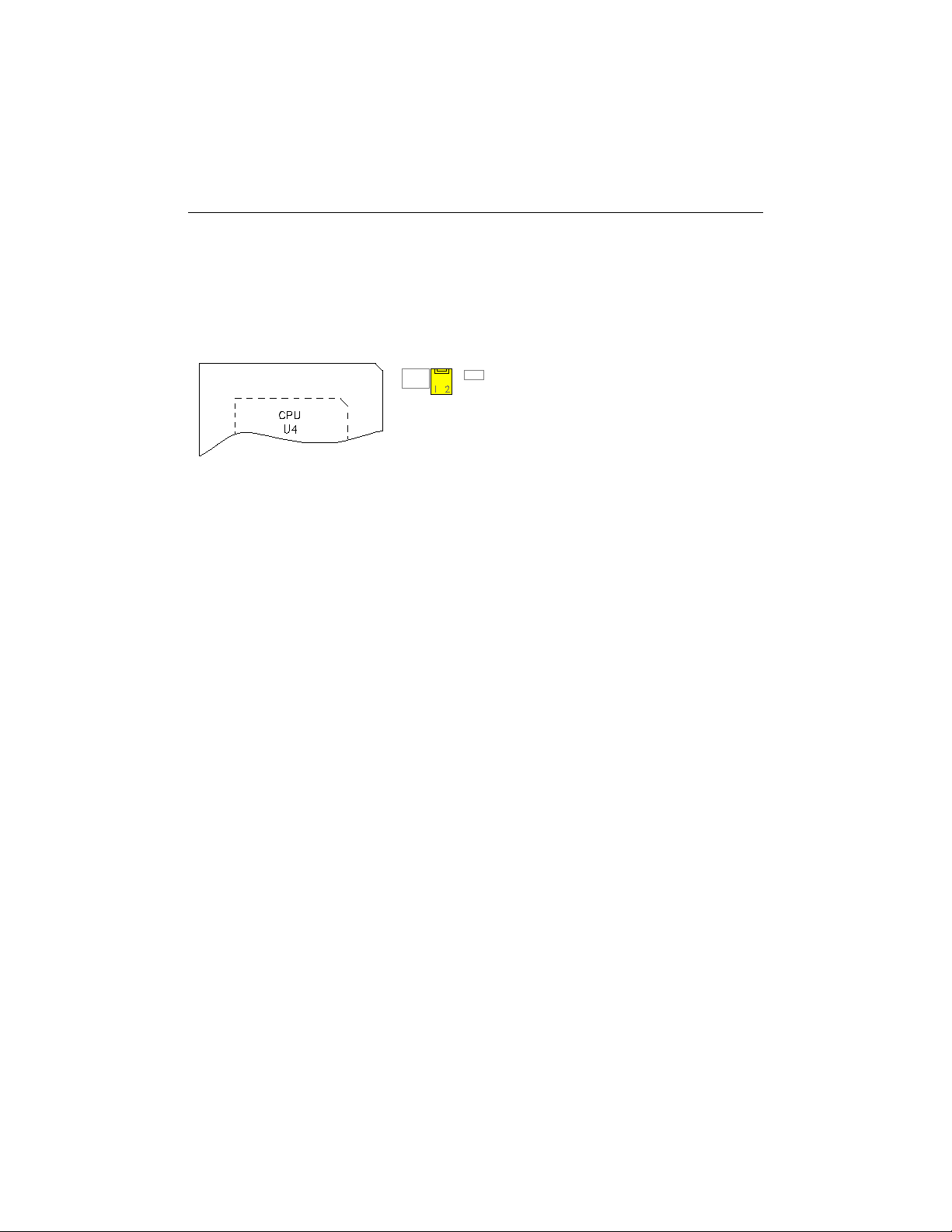
The fan connector appears as follows:
DIAGRAM 6-1: J17 Fan Connector
Installing and Working with System Components
J17
CPU Fan
W3
The fan connector’s pinout is as follows:
Pin 1: +12V
W23
Pin 2: GND
The following list includes approved vendors for the J17 connector’s mating parts:
Leoco 2530 S020013 (housing),
Leoco 2533 TCB00A0 (crimp);
Molex 22-01-3027 (housing),
Molex 08-50-0114 (crimp).
6.3. ENABLING CACHE MEMORY
There are two separate caches in the host subsystem: internal cache and external cache. The
cache inside the processor (internal cache) is referred to as the first level cache (also primary
cache). The external cache (called system cache in this manual) comprises the System
Controller’s cache control circuitry and associated external memory array; it is referred to as
the second level cache (also secondary cache). The second level cache is unified, which means
that both CPU data and instructions are stored in the cache.
System cache is enabled and configured in the AWARD BIOS Setup program (details in
Section 14 - Software Setup).
6-5
Page 32
PCI-936 Technical Reference Manual
6.4. SELECTING BIOS BOOT OPTIONS
By default, the PCI-936 boots with the BIOS contained into the Boot Block Flash. The Boot
Block Flash consists in a flash memory device with verification and protection features that
merges the entire BIOS code and a protected emergency code.
The Boot Block Flash appears as the easiest way to upgrade the board’s BIOS as its version
changes, or in case of a programming error or a data corruption.
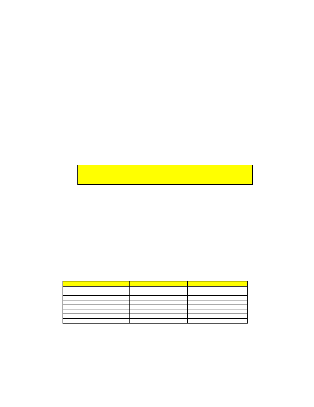
In the case of a BIOS corruption, the PCI-936 provides an emergency boot jumper (J13).
When the emergency boot is enabled (jumper J13 shorted), an emergency procedure is
executed to update the BIOS code from a DOS file located on an emergency disk.
✏✏✏✏
The complete procedure to execute an emergency boot is described in Section F.2 (Emergency
Procedure).
Note:
A BIOS corruption is one of the symptoms of a non-functional board: it may be
caused by an electrical shutdown that occurs before a BIOS update operation is
completed.
6.5. INSTALLING SUPERVISOR UTILITIES
6.5.1 SUPERVISOR I/O REGISTERS
Two supervisor I/O registers are provided to set and control special features of the board such
as: watchdog, Flash, RS-485, and power fail output. These registers are two 8-bit registers that
can be located at three different I/O addresses, 190h/193h, 290h/293h or 390h/393h, using the
J19 jumper. Each register is bit read and write accessible; however, some are reserved for
internal requirements. They are described as follows:
TABLE 6-3: Register 190H, 290H or 390H
Bit # Bit Value * Function WRITE mode: READ mode:
0 0 Enable Watchdog 1=Enable / 0= Disable* Same
1 1 Watchdog pulse write 1-0 alternately to refresh Same
2 0 Flash programming 1= Enable / 0= Disable (+12V) Same
3 0 RS-485 direction 1= Read only / 0= Write only Power Detect. or Batt. Low output
4 0 Reserved W22 (7-8) Status
5 0 Reserved W22 (5-6) Status
6 1 Reserved W22 (3-4) Status
7 0 Reserved W22 (1-2) Status
* Default values
6-6
Page 33
Installing and Working with System Components
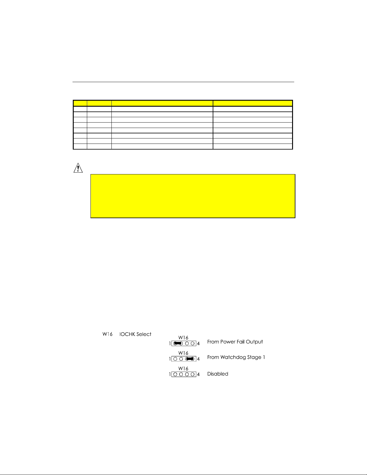
TABLE 6-4: Register 193H, 293H or 393H
Bit # Bit Value * WRITE Function: READ Function:
0 0/1 Reserved ** R/W Reserved
1 0/1 Reserved ** R/W Reserved
2 1 Dual Stage Watchdog R/W ; 1: Disable 0: Enable Same
3 1 Clear History ; 1: Normal 0: Clear 1: Last reset caused by watchdog
4 0 Reserved 1: Last reset caused by push-button reset
5 0 Reserved 0: First level watchdog timed out
6 0/1 Reserved Reserved, SADI
7 0 Reserved* R/W Reserved
* Default values ** Read and mask before changing bits
Cautions:
1. Not all bits are R/W. Therefore, be certain to keep a mirror image of the
register when programming it.
2. All bits are 0 after a hardware RESET or power up condition.
3. Write the values shown in the "Bit Value (Default)" column if you are
unsure.
As the supervisor I/O registers provide features associated to the TEKNOR Extension, the
TEKNOR Extension mode must be enabled using the W22 jumper which controls the
extended BIOS modes of the board (refer to Section 12 - Setting Jumpers).
6.5.2 POWER FAIL DETECTION
Power failure conditions may be detected if a low backup battery condition occurs, or the
monitored +5V power supply falls below 4.75V.
If either of the two above conditions occur, the PFO (Power Fail Output signal) goes low.
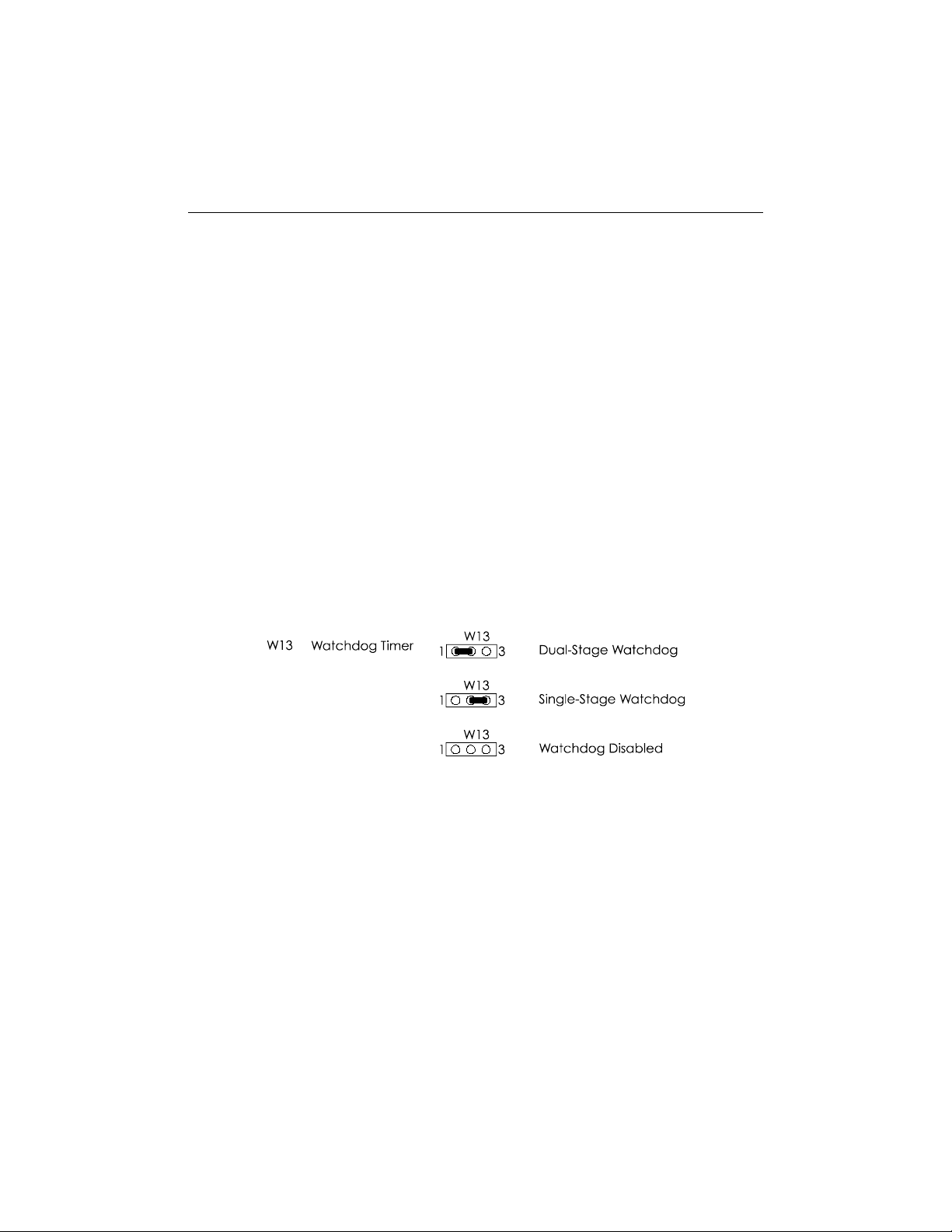
To generate a non-maskable interrupt (NMI) when the PFO goes low, set W16 jumper to
position 1-2.
6-7
Page 34
PCI-936 Technical Reference Manual
6.5.3 WATCHDOG DETECTION
The single stage watchdog time-out detector is used to monitor the output of the first stage
watchdog time-out.
To generate a non-maskable interrupt (NMI) when the first stage watchdog times out, set the
W16 jumper to position 3-4.
6.5.4 WATCHDOG TIMERS
The Watchdog is used to control the CPU inactivity. It functions according to a specified
duration of inactivity from when it will reset the CPU.
The watchdog can be: Dual-Stage, Single-Stage, or disabled, using W13 jumper for setting.
Jumper W13 must be installed to enable one watchdog configuration. If removed, the
watchdog is disabled.
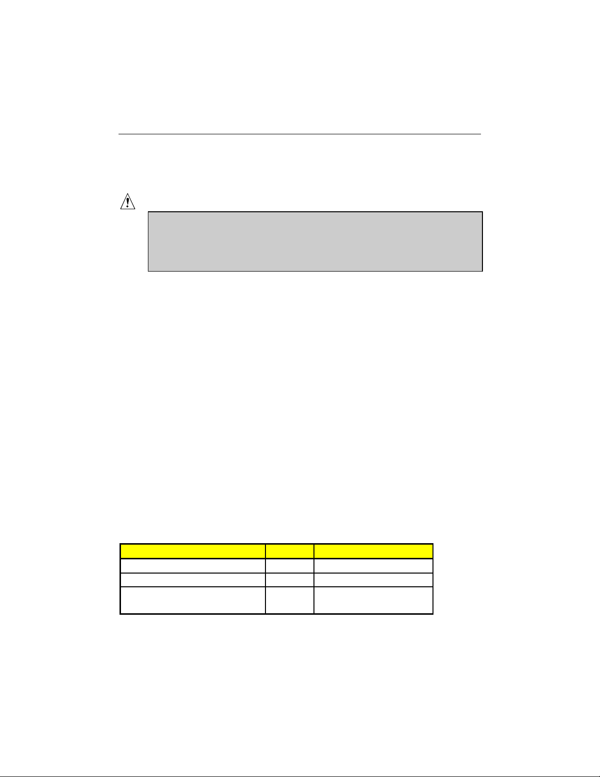
The W13 settings are shown below (* = initial setting):
Single Stage Watchdog:
The first stage Watchdog must also be enabled and refreshed by software. To enable the first
stage Watchdog by software, first write "1" in bit "0" at address 190H (or at 290H or 390H
depending on the W19 jumper setting).
When enabled, the microprocessor must refresh the first stage Watchdog. This is done by
writing alternatively "0" and "1" to bit 1 at address 190H (or at 290H or 390H), once every
1.6 seconds to verify proper software execution.
Following a reset, the Watchdog is always disabled.
6-8
Page 35
Installing and Working with System Components
If a hardware or software failure occurs such that the watchdog is not refreshed, a reset pulse is
generated by the Watchdog to restart the processor.
Caution:
The user program must provide the first access to address 190H (or at 290H or
390H depending on the W19 jumper setting), and must also include the refresh
routine. In addition, be certain to keep a mirror image of register 190H (or 290H
or 390H) when programming it. This is necessary since the register is a writeonly user register and, as a result, is not used by the system BIOS.
Dual Stage Watchdog
The dual stage watchdog consists of two watchdogs (MAX691) in cascade and is enabled and
refreshed similarly to the single stage watchdog.
To enable the dual stage watchdog, first write “1” in bit “0” at address 190H (or at 290H or
390H, depending on the W19 jumper setting). Then write “0” in bit “2” at address 193H (or at
293H or 393H, depending on the W19 jumper setting).
When enabled, the microprocessor must refresh the first stage Watchdog. This is done by
writing alternatively “0” and “1” to bit 1 at address 190H (or at 290H or 390H), once every
1.6 second to verify proper software execution.
If a hardware or software failure occurs such as the first Watchdog is not refreshed, its timeout output (WDO1), when tied to ISA’s IOCHK signal (jumper W16 set to 3-4), can be used
to generate a NMI to the CPU. In this case, the interrupt service routine could try to correct the
failure and re-enable pulses to the first Watchdog. The service routine has 1.6 second to
resume normal operation of the system otherwise the second Watchdog times-out and resets
the system.
TABLE 6-5: Watchdog Timer Register
Address Status Register
190H, 290H OR 390H: Bit 0 Read/Write Watchdog enable
190H, 290H OR 390H: Bit 1 Read/Write Watchdog refresh
193H, 293H OR 393H: Bit 5 Read Only First Stage Watchdog Status
1: Normal 0: Timed Out
6-9
Page 36
PCI-936 Technical Reference Manual
6.5.5 SYSTEM RESET HISTORY STATUS
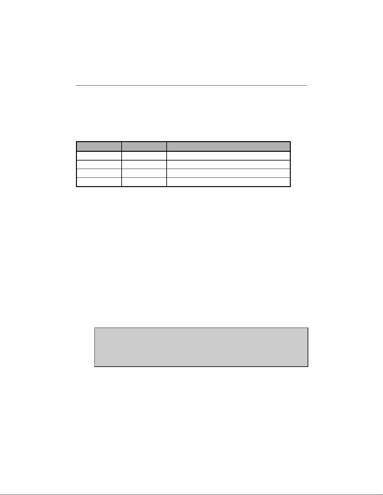
A special circuit allows the user to determine the cause of the last system reset. The bits 3
and 4 at address 193H or (293H or 393H) record the following possibilities:
TABLE 6-6: System Reset History Status
Bit 4: PBRES BIT 3: WDO Description
0 0 Normal Operation
0 1 Watchdog caused the last system reset
1 0 Push-button reset caused the last system reset
1 1 Undetermined
To reset the status, write “0” the “1” in bit “3” at address 193H or (293H or 393H). After
this operation, PBRES (bit 4) and WDO (bit 3) should be set to “0”. The bits are also reset
after a power-up.
6.6. INSTALLING PCI-936 IN PASSIVE BACKPLANE
The PCI-936 will operate on any PCI-ISA passive backplane, provided it complies with the
PCI INDUSTRIAL COMPUTER MANUFACTURERS GROUP, Revision 2.1 specification.
The board may be installed into a TEK-950 PCI-ISA Passive Backplane, which has three PCI
slots, five ISA slots, and a PCI-ISA for the Industrial Single Board Computer.
Since the PCI-936 is also fully IBM AT compatible, it can also be installed on any standard
ISA passive backplane, if PCI expansion slots are not needed.
✏✏✏✏
Note:
The PCI-936 chipset does not support address stepping (described in the PCI Local
Bus Specification). To ensure proper detection of PCI adapter cards, 33Ω or less
resistors should be used on the backplane’s ID SELECT signal address lines (between
the CPU slot and each PCI slot. All Kontronm PCI backplanes include this specific
feature. For more information, contact Kontron’s Technical Support department.
6-10
Page 37
Installing and Working with System Components
6.7. CONNECTING INTERFACE DEVICES (KEYBOARD, SPEAKER, RESET, LED)
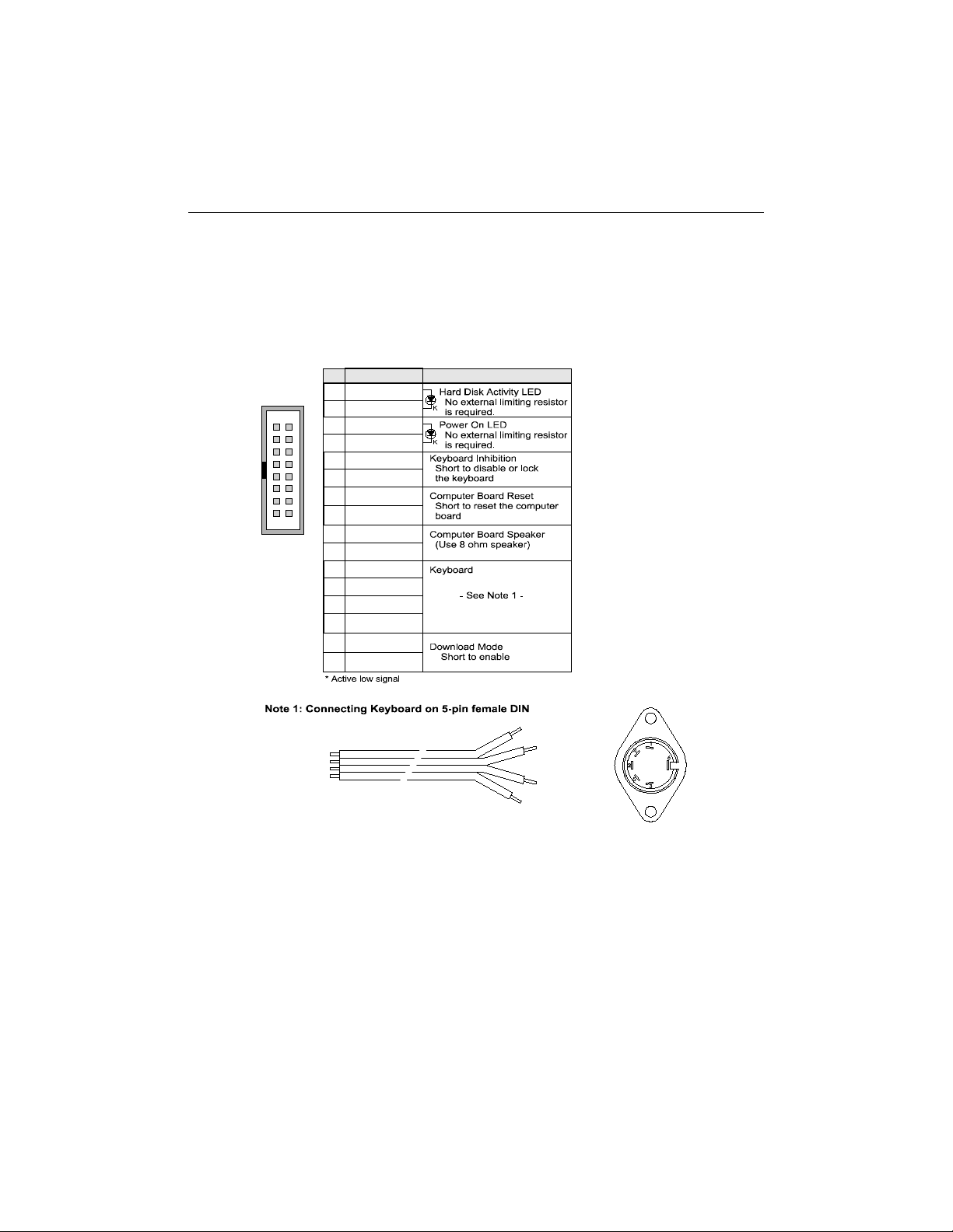
Connector J4 provides all the necessary signals for connecting the keyboard, speaker, reset,
and keylock interface devices. It is described as follows:
Signals Name Descrip tion
VCC (+5V)
16
ACT1*
1152
15
VCC (+5V)
6
GND
4
9
KBINH
10
GND
13
PBRES*
14
7
8
1
3
2
5
11
12
GND
SPKR
VCC (+5V)
KCLK
KDAT
GND
VCC (+5V)
DOWNLD*
GND
16
To Pi n #1
KCLK
KDAT
GND
VCC (+5V)
To P in #2
To Pin #4, 6
To Pi n# 5
(Connector back view)
The following list includes approved vendors for the J4 connector’s mating parts:
Amp 746285-3 [optional strain relief: 499252-8],
Robinson Nugent IDS-C16PK-TG,
Thomas & Betts 622-1630 [optional strain relief: 622-1641].
(16-pin flat cable connector).
6-11
Page 38
PCI-936 Technical Reference Manual
6.8. CONNECTING A MONITOR
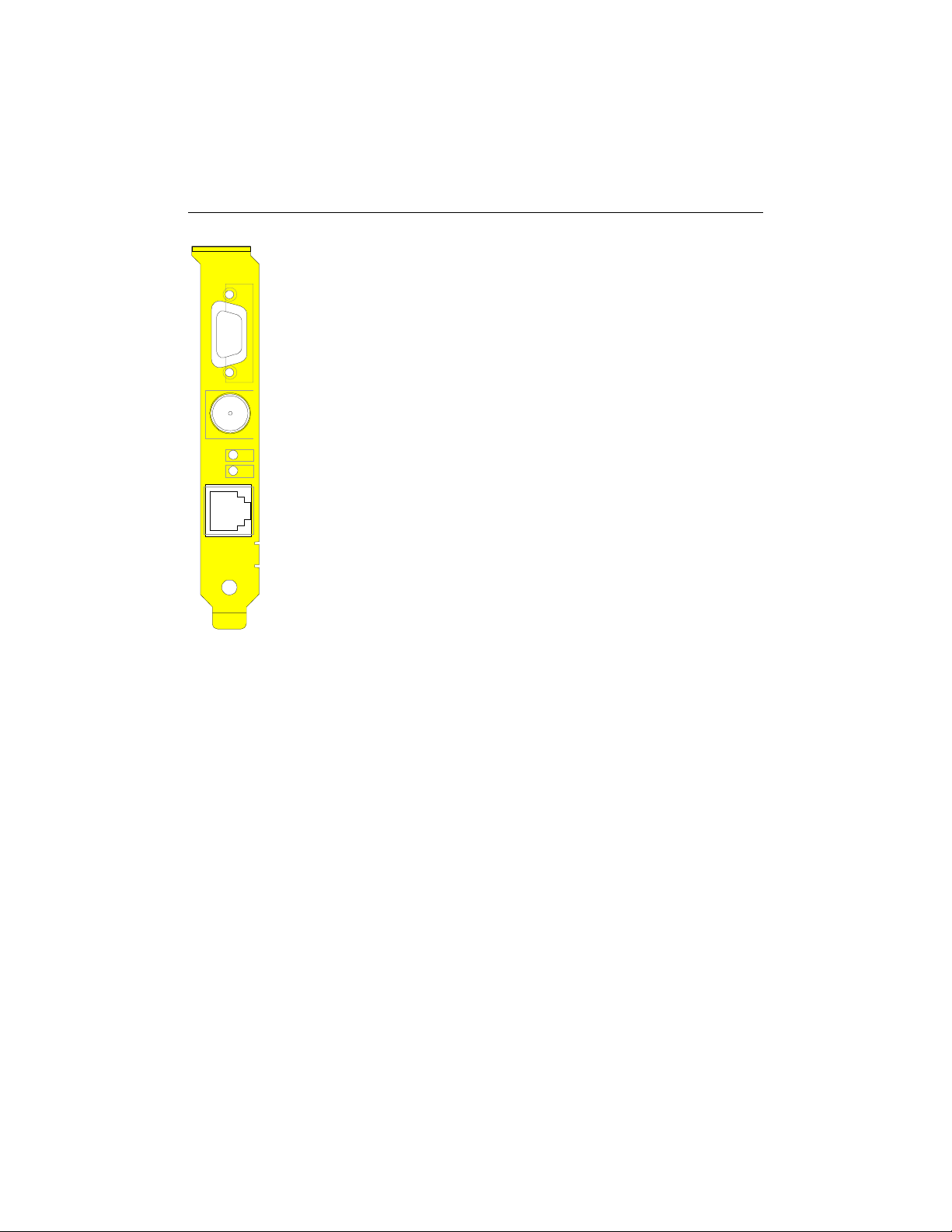
The CRT monitor connects directly to J15: standard VGA DB15
female connector.
J15
6.9. CONNECTING A MOUSE
J16
JDS2
JDS3
J18
The PS/2 mouse may be directly connected to a standard connector
(J16) available on the board’s bracket. Mouse signals are also
available through the J25 4-pin header.
6-12
Page 39
6-13
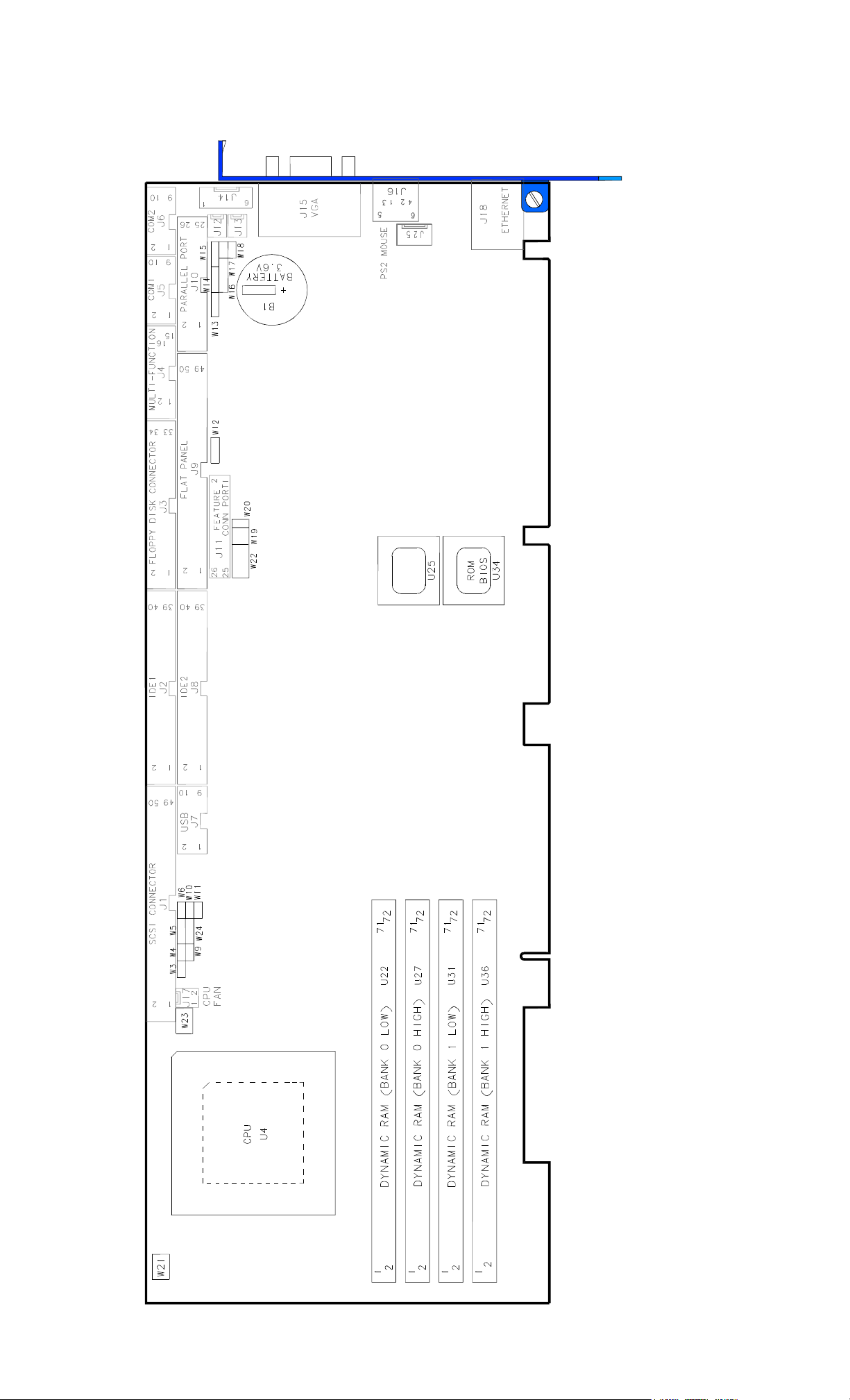
SYSTEM COMPONENT OVERVIEW
Page 40

Page 41
7. INSTALLING STORAGE DEVICES
7.1. CONNECTING A FLOPPY DRIVE
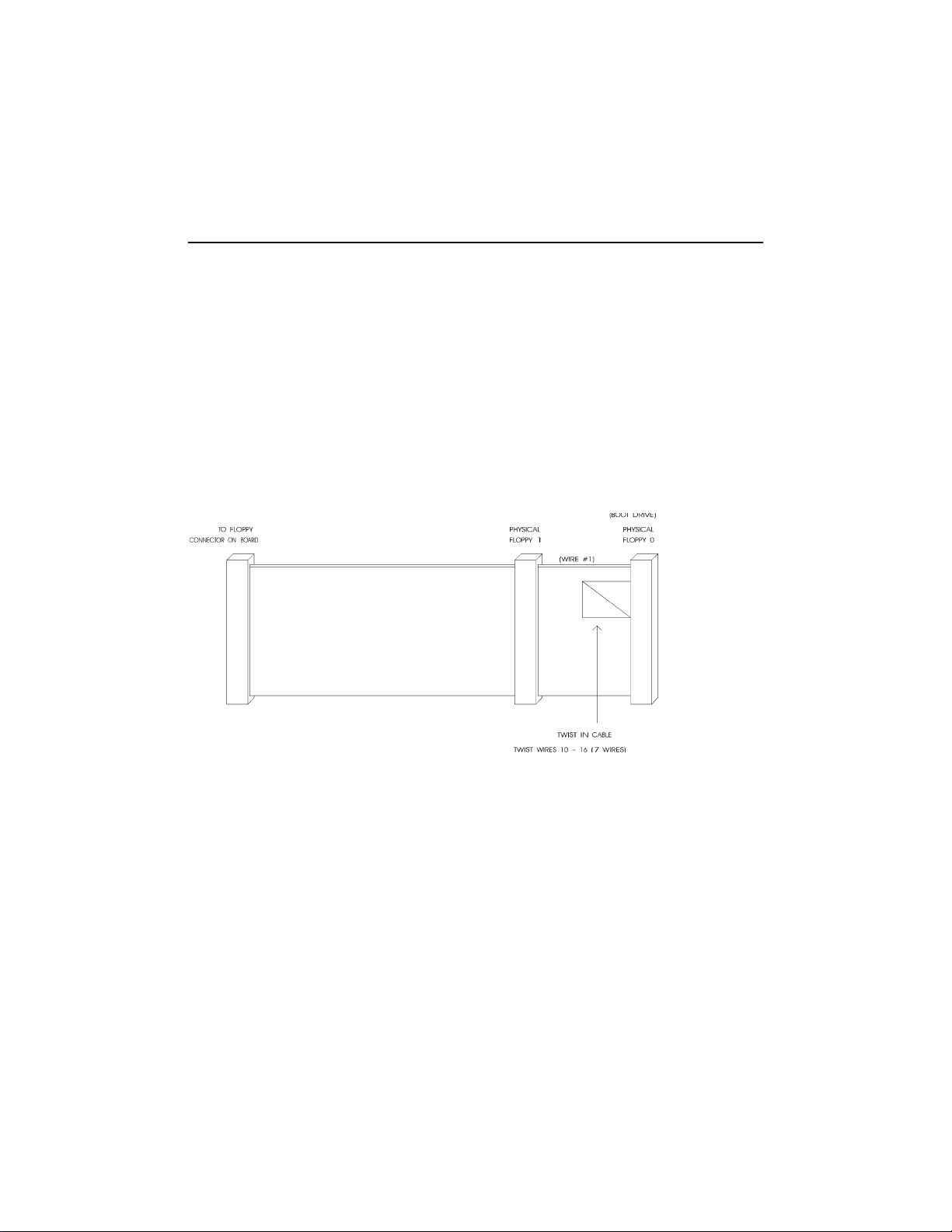
The installation of the floppy drives is done via a standard IBM 34-pin flat ribbon cable that
connects to J3.
The following list includes approved vendors for the J3 connector’s mating parts:
Amp 746285-8 [optional strain relief: 499252-6],
Robinson Nugent IDS-C34PK-TG,
Thomas & Betts 622-3430 [optional strain relief: 622-3441].
(34-pin flat cable connector).
DIAGRAM 7-2: Floppy Disk Cable
7-1
Page 42

PCI-936 Technical Reference Manual
7.1.1 FLOPPY SOFTWARE SETUP
AWARD Setup
Starting from the AWARD Setup program main menu, use the following procedure to
complete the setup:
• From the Main Menu, select the Standard CMOS Setup option.
• In the Standard CMOS Setup menu, use the arrow keys to highlight the Drive A: or Drive
B: option (depending on the installation of your Floppy drive).
− Select the category identifying the types of Floppy disk drive A or drive B that have
been installed in the computer.
TABLE 7-1: Floppy Drive options
Option Description
None No Floppy drive installed.
360KB, 5.25 in. 5-1/4 inch PC-type standard drive; 360KB capacity.
1.2MB, 5.25 in. 5-1/4 inch AT-type high-density drive; 1.2MB capacity.
720KB, 3.5 in. 3-1/2 inch double-sided drive; 720KB capacity.
1.44MB, 3.5 in. 3-1/2 inch double-sided drive; 1.44MB capacity.
2.88MB, 3.5 in. 3-1/2 inch double-sided drive; 2.88MB capacity.
7.1.2 FLOPPY CONNECTOR PINOUT
Please refer to the J3 Floppy connector’s pinout in Section D-7 (Connector Pinouts).
7-2
Page 43

Installing Storage Devices
7.2. ENHANCED IDE DEVICES
7.2.1 ENHANCED IDE CONNECTORS LOCATION & HOOK-UP
For hooking up either IDE connector, a 40-pin dual row header signal connector is required.
This connector handles all command, data and status I/O lines. Its maximum cable length is 18
inches. It connects directly with the onboard 40-pin male header connector at J2 or J8.
The following list includes approved vendors for the J2 and J8 connectors’ mating parts:
Amp 746285-9 [optional strain relief: 499252-1],
Robinson Nugent IDS-C40PK-TG,
Thomas & Betts 622-4030 [optional strain relief: 622-4041].
(40-pin flat cable connector).
The drive itself can be mounted on any horizontal or vertical plane.
7-3
Page 44
PCI-936 Technical Reference Manual
7.3. SCSI DEVICES
7.3.1 INSTALLING A FIXED SCSI HARD DISK
This section will explain how to go about installing a fixed SCSI Hard Disk on your system.
No additional hardware or drivers are necessary if no more than two IDE/SCSI hard disks
will be present in your system.
To install your fixed SCSI hard disk, these steps must be followed:
7.3.1.1. VIP-UP Setup
The VIP-UP software utility must be used prior to physically installing the SCSI hard disk.
The onboard SCSI controller/BIOS option of the VIP-UP screen must be set at Enabled.
When done, update your VIP-UP Setup by pressing the F10 key.
You must not "install" your SCSI hard disk type in AWARD BIOS Setup (only your IDE
hard disk).
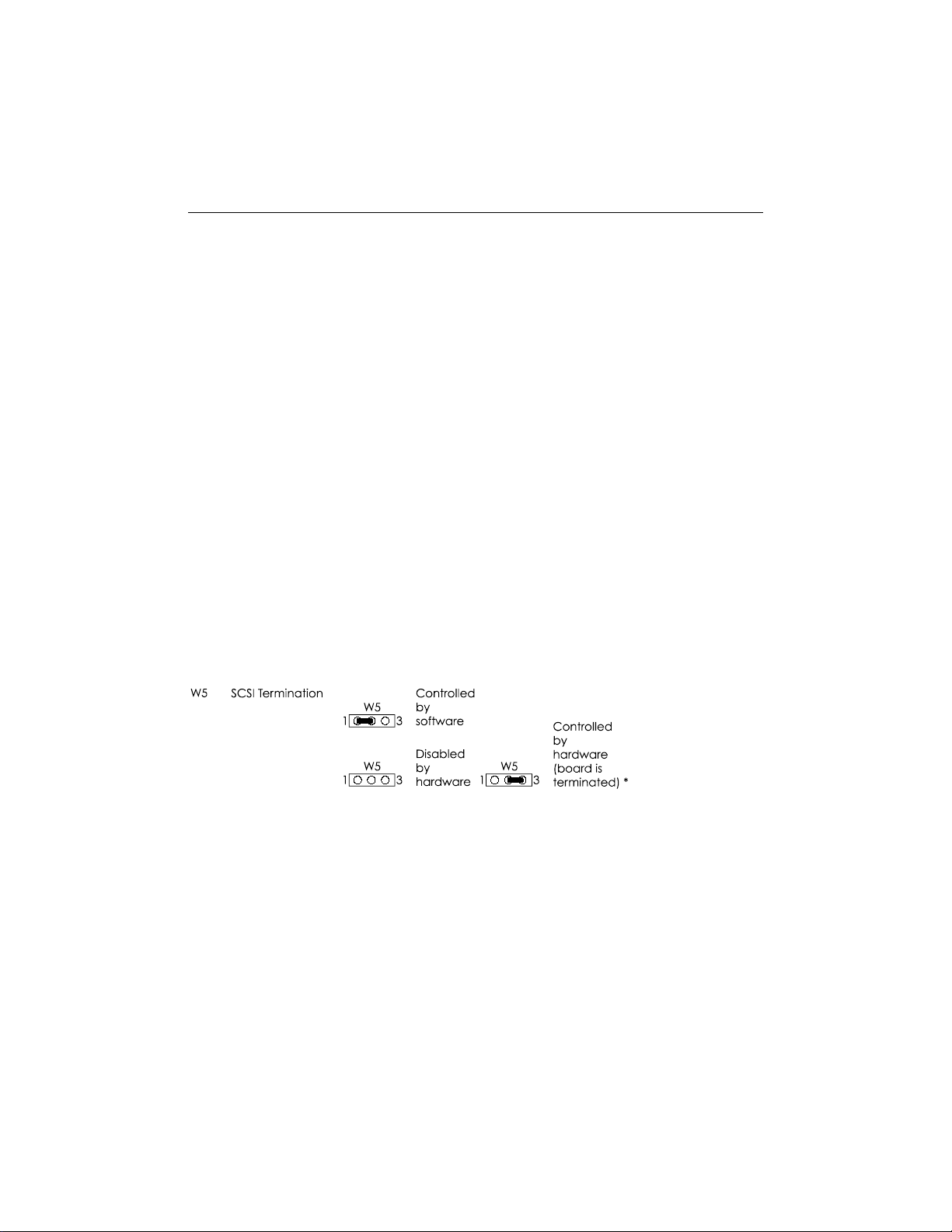
7.3.1.2. Jumpers
The PCI-936 board's initial jumper settings should be kept in most cases, unless there is a
conflict with other devices you have installed (* = initial setting).
7.3.1.3. SCSI Cable
Make sure that both ends, and only each end, of the SCSI cable is terminated.
Approved vendors for mating parts are listed below:
Amp 1-746285-0 [499252-4*],
Robinson Nugent IDS-C50PK-TG,
Thomas & Betts 622-5030 [622-55041*].
(50-pin flat cable connector).
7-4
Page 45

Installing Storage Devices
Attach one end of the SCSI cable to the J1 SCSI 50-pin connector. Make sure line 1 of the
cable is matched with pin 1 of connector J1.
Attach the other end to your SCSI device, making sure line 1 is matched with pin 1 on your
device.
You must also install a cable from your power supply to your SCSI device.
7.3.1.4. Software setting
Follow installation instructions provided with your SCSI peripheral device.
Caution:
Each device must be assigned a unique identifier called a SCSI Target ID. The
lower the ID, the lower the priority level of the device in the SCSI subsystem. The
host adapter is usually assigned the highest priority level (15 or 7). Table 7-4 lists
common SCSI Target IDs.
To change SCSI parameters, press CTRL-C when prompt during boot-up.
TABLE 7-2: Common SCSI Target IDs
SCSI Device Commonly Used IDs
Host Adapter 15 or 7
Hard Disks 0,1,2,3
CD-ROM 4,5
Tape drive 5,6
7.3.2 INSTALLING OTHER SCSI DEVICES
To install any of the following: CD-ROM, Magneto-Optical/Removable Disk Drive, Tape
Drive, Write Once Read Many (WORM) and scanners, please use the SCSI diskette that
you received with your PCI-936. A special utility will install all the necessary drivers.
7-5
Page 46
7-6
PCI-936 Technical Reference Manual
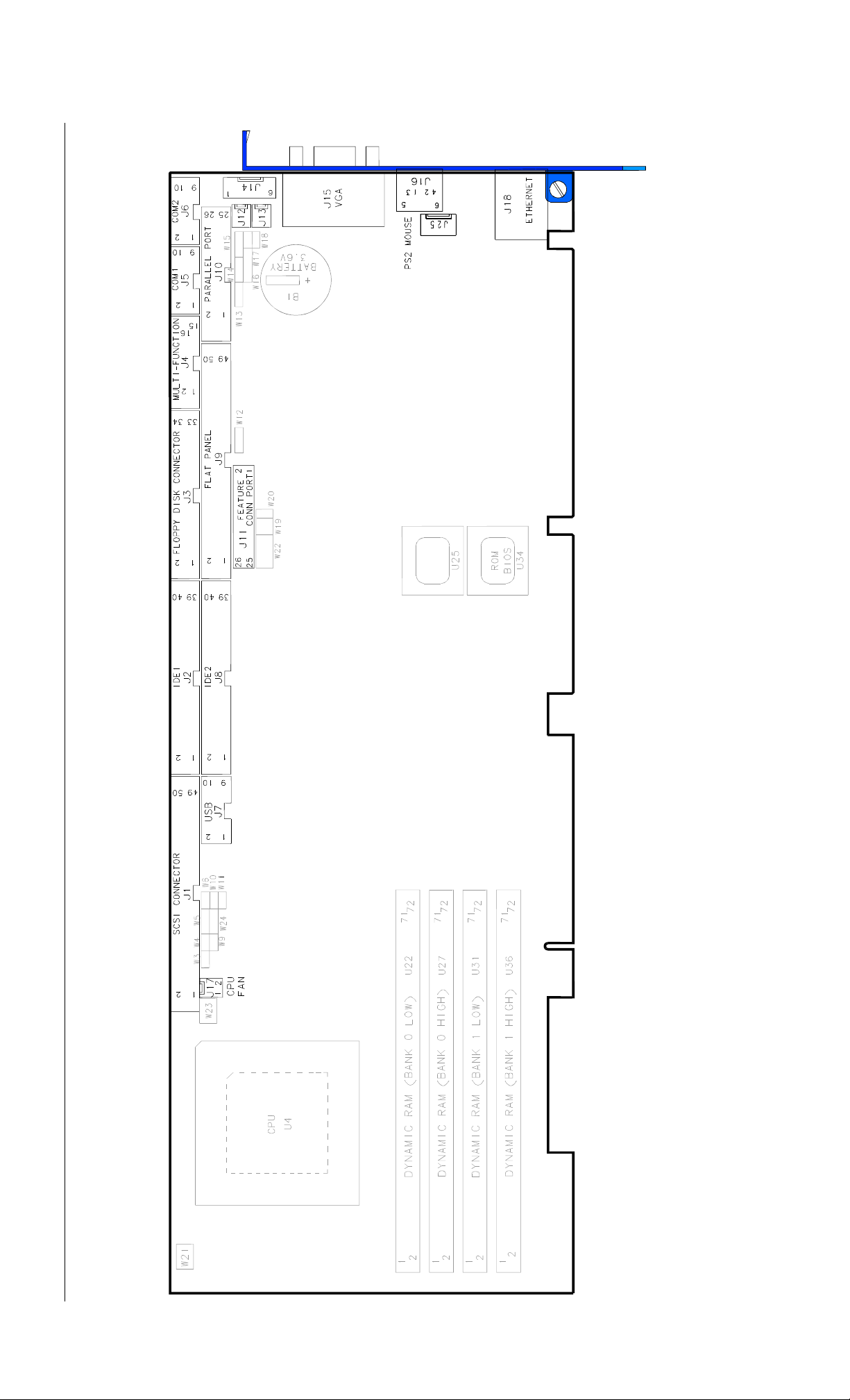
CONNECTOR LOCATION
Page 47

8. INSTALLING VIDEO
8.1. VIDEO CONTROLLER
8.1.1 INSTALLING VIDEO DRIVERS
The video controller has specific drivers for various operating systems. Drivers, must be
installed using the Utility Disk containing the video drivers, which came with your PCI-936.
For any driver that is not on the Utility Disk, please contact the Technical Support department.
8.1.2 DISABLING VIDEO CONTROLLER
The video controller can be disabled by shorting pins 7 and 8 on the W22 jumper.
This feature is useful when an external video card is required for testing or other purposes.
8.2. INSTALLING CRT VIDEO DISPLAY
8.2.1 CONNECTING CRT VIDEO DISPLAY
The CRT display connects directly to the standard VGA DB15 female on the edge bracket.
The complete connector pinout is given Section C-3.
8.2.2 VPORT
The PCI-936 supports an external 8-bit VPORT via 26-pin male header. This VPORT is
compatible with Kontron’s VIPer vision TEK-380 interface, but the PCI-936 board does
not provide mounting holes for attachment of the TEK-380. The TEK-380 can be
connected through a ribbon cable and the power is supplied by the VPORT connector.
8-1
Page 48
PCI-936 Technical Reference Manual
8.3. FLAT PANEL
8.3.1 FLAT PANEL CONNECTOR PINOUT
When connecting a flat panel, customized cable is needed to connect the panel to the board.
The pinout of this cable depends on the Flat Panel model you use.
8.3.2 FLAT PANEL INSTALLATION
The myriad of Flat Panel displays available makes it virtually impossible for us to show every
type of configuration that exists. For your convenience, we have published the PCI-936 FLAT
PANEL CONFIGURATION GUIDE; this handy manual charts out the cabling, jumper
settings, and other special requirements for some of the most popular displays.
The name of the Flat Panel BIOS file (.BFP extension) to be used to update the Flash EPROM
BIOS is also included in that guide; refer to Section 17 to perform a VGA BIOS file update
with the UBIOS software.
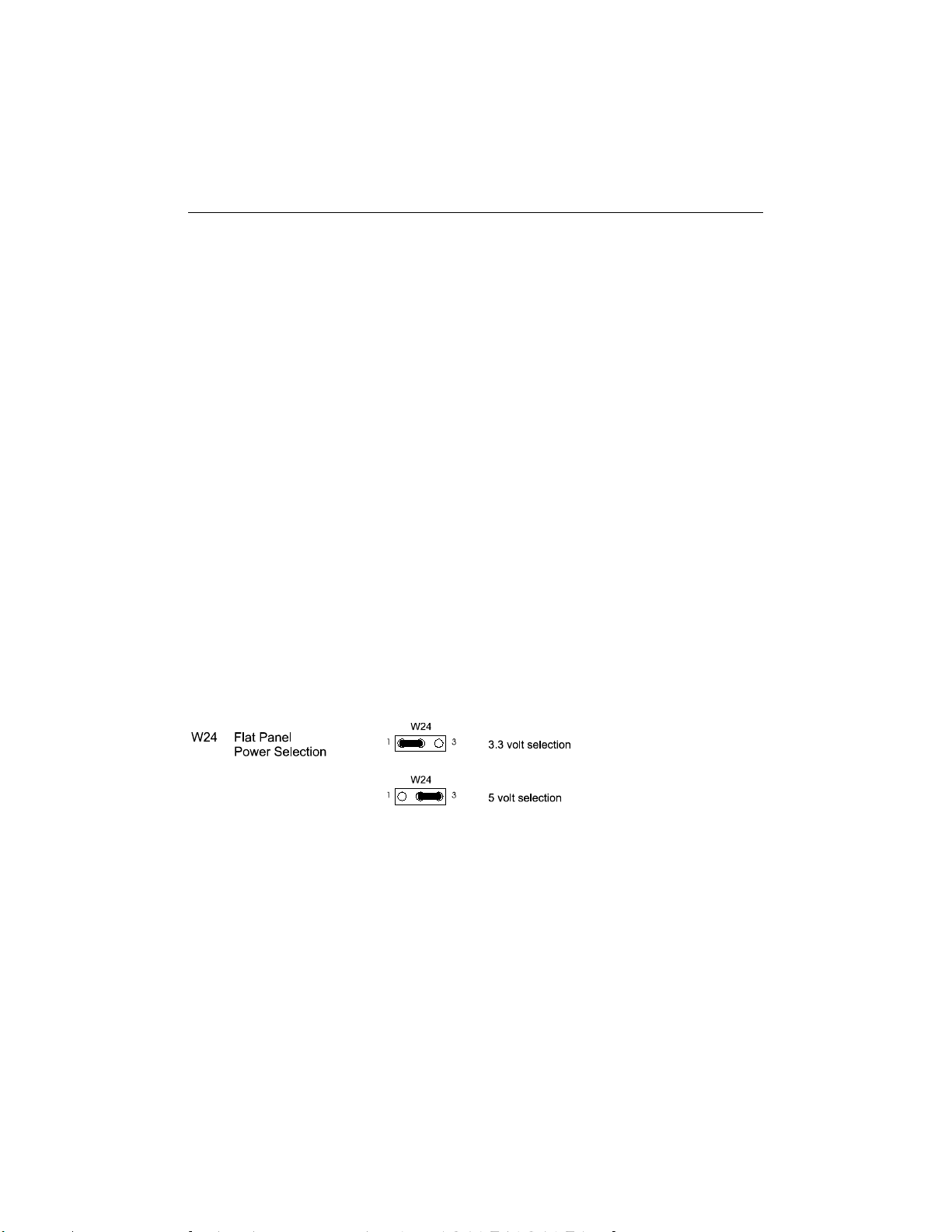
8.3.2.1. FLAT PANEL POWER SUPPLY SELECTION
PCI-936 supports 3.3-Volt and 5-Volt power for flat panel. The selection of the flat panel
power supply using the jumper W24 setting are shown below.
Please contact our Sales or Technical Support departments for more information on Flat Panel
applications.
8-2
Page 49

9. INSTALLING PERIPHERALS
9.1. SERIAL PORTS
Two serial ports are provided on the TEK-936. They are 16C550 compatible serial ports
which have internal 16-byte FIFO buffers for more efficient data transfers.
Serial Port 1 is buffered for RS-232 operations, while Serial Port 2 may be set as RS-232 or
RS-422/RS-485.
The following list includes approved vendors for the J5 and J6 connectors’ mating parts:
Amp 746285-1 [optional strain relief: 499252-5],
Robinson Nugent IDS-C10PK-TG,
Thomas & Betts 622-1030 [optional strain relief: 622-1041].
(10-pin flat cable connector).
For information on the programming of serial ports with the use of FIFO buffers, ask for
Application Note # AN93007 from Kontron’s Technical Support department.
9-1
Page 50
PCI-936 Technical Reference Manual
9.1.1 Serial Port 1 (J5) RS-232
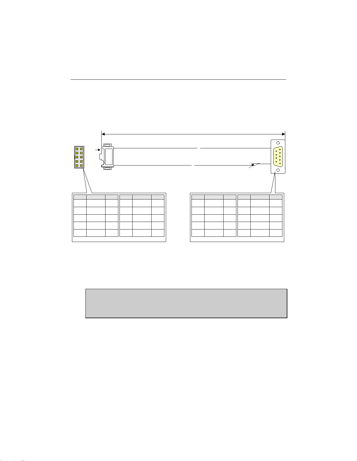
The Serial Port 1 is configured as RS-232. With the IBM 9-pin DSUB Standard, Serial Port 1
is 100% compatible with the IBM-AT serial port.
18''
Onboard
10-pin Header
1
2
Pin 1
9
10
I
DCD
I
SIN
O
SOUT
O
DTR
-
GND
Female
10-pin Header
1
3
5
7
9
RS-232 Serial Port Flat C able (150 -019)
SignalSignal
DSR
2
RTS
4
CTS
6
RI
8
N.C.
10
I
O
I
I
-
I
DSR
O
RTS
I
CTS
I
RI
9-pin Ma le D SUB Connecto r according to IBM-AT stand ardOnboard Seri al Port C onnect or
Cut Wire #10
Pin #Pin #
6
7
8
9
DB9 Male
Connector
Pin #Pin # I/OI/O I/OI/O
SignalSignal
DCD
1
RX
2
TX
3
DTR
4
Gnd
5
1
6
9
5
I
I
I
O
-
Kontron offers a 10-pin header to 9-pin DSUB cable for IBM-AT compatibility. This can be
purchased from Kontron or a cable can be made with a flat cable, a 10-pin flat cable crimp
header and a 9-pin DSUB flat cable crimp connector.
✏✏✏✏
Note:
The use of Taiwanese adapter cables is not recommended, since the pinout is often
incorrect. The direct crimp design offered by Kontron allows the simplest cable
assembly. All these cables are available from Kontron by contacting the Sales
Department.
9-2
Page 51
Installing Peripherals
9.1.2 Serial Port 2 (J6)
By default, the Serial Port 2 is set as RS-232. In this configuration, it functions the same as
Serial Port 1, with the same pinout. however, the Serial Port 2 may be set for RS-422/RS-485
operations, using the VIP-UP application.
9.1.2.1. RS-232 Mode
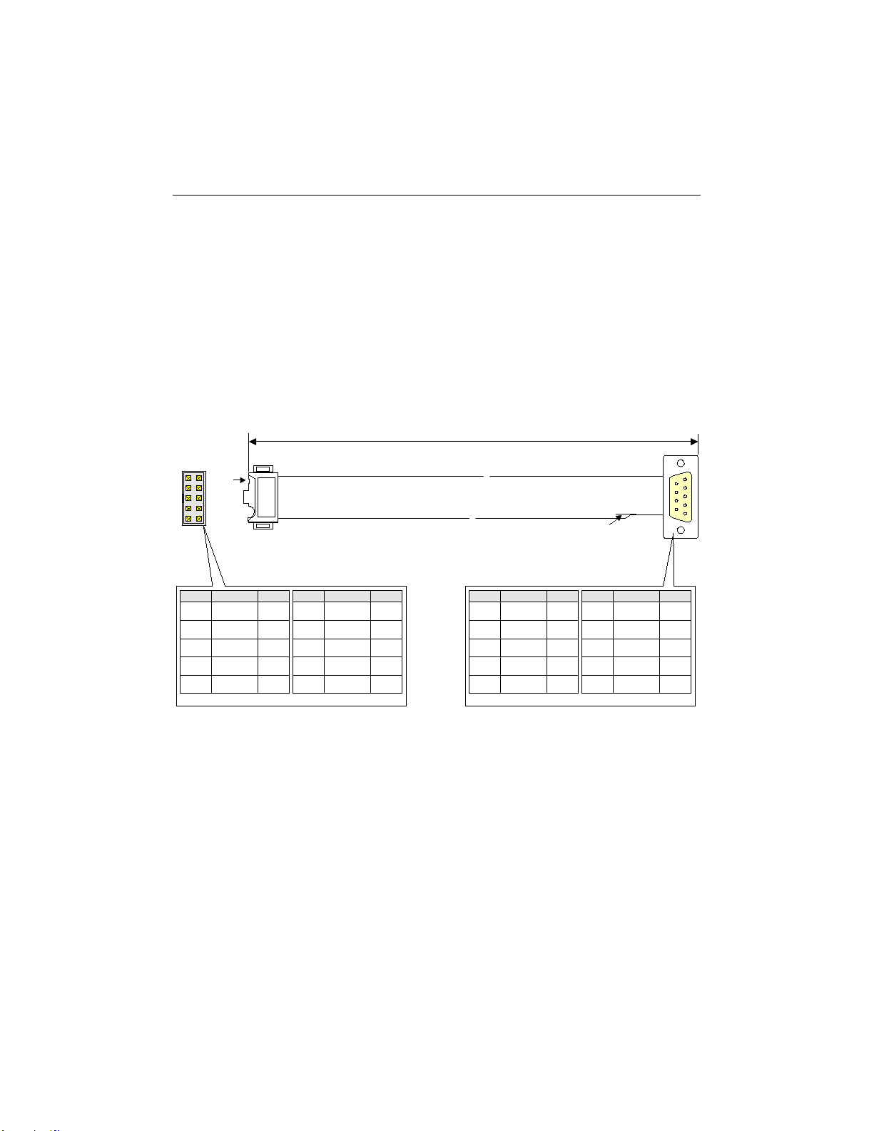
As an RS-232 port, and with the IBM 9-pin DSUB Standard, Serial Port 2 is 100% compatible
with the IBM-AT serial port. To output RS-232 signals from the 10-pin onboard connector to
a 9-pin DSUB connector, please refer to the following diagram:
18''
Onboard
10-pin Header
1
2
Pin 1
9
10
I
DCD
I
SIN
O
SOUT
O
DTR
-
GND
Female
10-pin Header
1
3
5
7
9
RS-232 Serial Port Flat C able (150 -019)
SignalSignal
DSR
2
RTS
4
CTS
6
RI
8
N.C.
10
I
O
I
I
-
I
DSR
O
RTS
I
CTS
I
RI
9-pin Ma le D SUB Connecto r according to IBM-AT stand ardOnboard Seri al Port C onnect or
Cut Wire #10
Pin #Pin #
6
7
8
9
DB9 Male
Connector
Pin #Pin # I/OI/O I/OI/O
SignalSignal
DCD
1
RX
2
TX
3
DTR
4
Gnd
5
1
6
9
5
I
I
I
O
-
Kontron offers a 10-pin header to 9-pin DSUB cable for IBM-AT compatibility. This can be
purchased from Kontron or a cable can be made with a flat cable, a 10-pin flat cable crimp
header and a 9-pin DSUB flat cable crimp connector. The direct crimp design offered by
Kontron allows the simplest cable assembly. All these cables are available from Kontron
by contacting the Sales department.
9-3
Page 52
PCI-936 Technical Reference Manual
SERIALPORT2
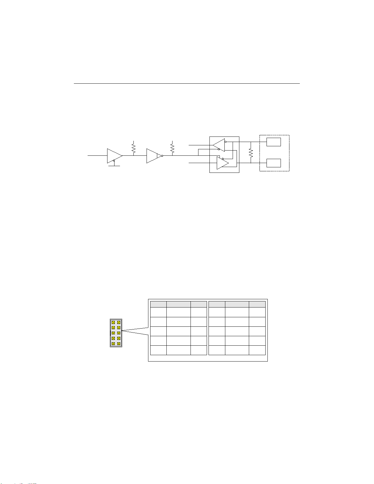
9.1.2.2. RS-422/RS-485 Mode
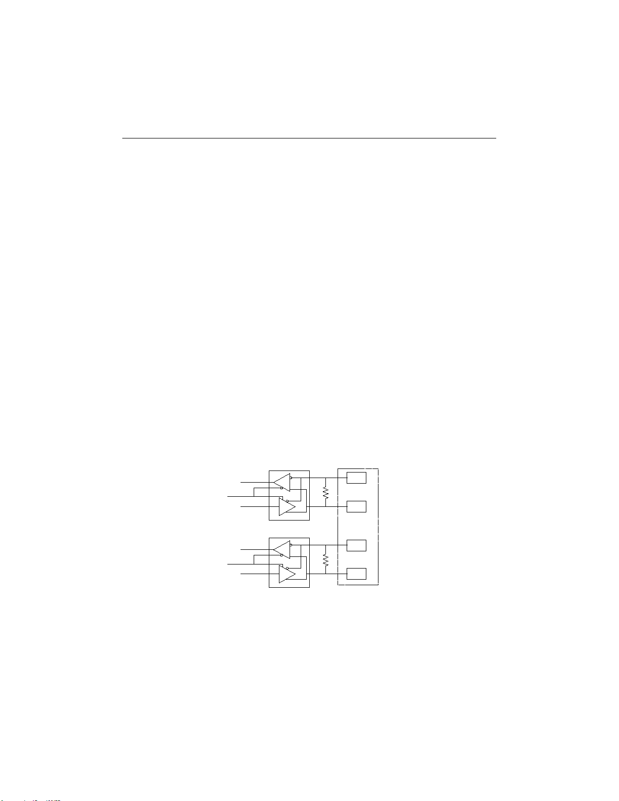
When configured for RS-422/RS-485 operations, the Serial Port 2 can transmit and receive
differential signals, in either full-duplex or party line communication.
Communicating with differential signals requires a pair of wires for the transmission and a pair
of wires for the reception (RS-422). For a better noise rejection, the use of twisted pair cable is
highly recommended. This will enable faster serial transmissions over greater distances than
with the common RS-232 protocol.
When using RS-422/485 mode, Serial Port 2 requires hardware and software settings:
. If required, use W17 and W18 jumpers to connect the RS-485 termination
resistance (RS-485 only)
. Select a logical COM port and matching address using the AMI BIOS setup
program (Available features are: Disabled, Auto, COM1/3F8h/IRQ4,
COM2/2F8h/IRQ3, COM3/3E8h/IRQ3, COM4/3E8h/IRQ4)
. Select the desired COM port operation mode (RS-422 or RS-485) using the VIP-
UP setup program
RS-422 - Full Duplex Operation: The RS-422 protocol uses both RX and TX lines during a
communication cession. Upon power-up or reset, the Serial Port 2 interface circuits are
automatically configured for full duplex operation: pins 3 and 4 of J6 act as the receiver lines
and pins 5 and 6 act as the transmitter lines.
10-PIN HEADER
120 ohms
RXD2
GND
X
LOW LOGIC LEVEL
LOW LOGIC LEVEL
X
VCC
TXD
75176
75176
7
6
120 ohms
7
6
1
2
3
4
1
2
3
4
3
RX-
4
RX+
3
TX-
4
TX+
There are no software implementation requirements except that software must not attempt to
use the handshake line because they are not connected. Therefore, software handshaking
(XON-XOFF) may be used.
9-4
Page 53
Installing Peripherals
SERIALPORT2
RS-485 - Party Line Operation: The RS-485 offers the ability to transmit and receive over
the same pair of wires (RX outputs: pins 3 and 4), and share the same communication line with
multiple stations. To ensure this configuration, only one system takes the control of the
communication line at the time.
10-PIN HEADER
3RX-
4RX+
RTS2
ENABLE
VCC
VCC
RXD2
TXD2
120 ohms
1
2
3
4
75176
7
6
The RS-485 protocol offers some advantages such as increased speed over long distances,
improved reliability over similar RS-232 setups, ability to share the transmission line, less
cabling requirements then RS-422 protocol, etc...
To enable party line operation, the software must write "1" to bit 3 at I/O register (at 190H,
290H or 390H base address, depending on W9 jumper). This allows the transceiver (pins 3
and 4 of J6) to be controlled by the RTS signal. Upon power-up or reset, the transceiver is by
default in "receiver mode" in order to preventing unwanted perturbation on the line.
In RS-485 mode, only both ends of the network must be terminated (120-ohm resistors).
Termination resistors (R188 and R189) are available on the PCI-936: If the board is installed
at on end of the network, these resistors may be installed using the W17 and W18 jumpers.
Pinout : When configured for RS-422/485 communication mode, the pin assignation for the
onboard Serial Port 2 appears as follows:
Pin #
Onboard
10-pin Header
1
2
9
10
Signa l
I
DCD
I/O
RX(-)
O
TX(-)
O
DTR
-
GND
Onboard Serial Port Connector set as RS-485
Pin # I/OI/O
1
3
5
7
9
10
Signal
DSR
2
RX(+)
4
TX(+)
6
RI
8
N.C.
I
O
I
I
-
9-5
Page 54
PCI-936 Technical Reference Manual
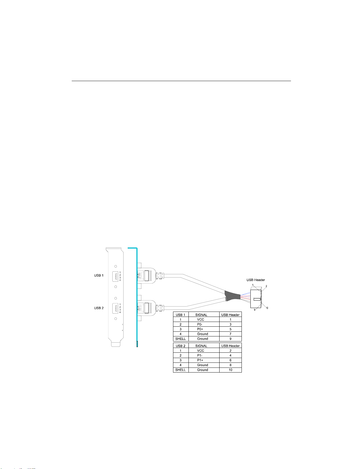
9.2. USB PORT (Connector - J7)
The USB port permits the direct connection of two USB connectors with an external hub.
The PCI-936 board fully supports the standard universal host controller interface (UHCI)
and uses standard software drivers that are UHCI-compatible. Features of the USB include:
. Plug and Play, Hot Plugable Peripherals and Power Management capabilities.
. Automatic mapping of function to driver and configuration.
. Support for isochronous and asynchronous transfer types over the same set of
wires.
. Support for up to 127 logical connections.
. Support for full speed (12Mbs) and low speed (1.5Mbs) USB connection. Full
speed connections require shielded cabling.
. Guaranteed bandwidth and low latencies appropriate for telephony, audio, and
other applications.
. Error handling and fault recovery mechanisms built into protocol.
The J7 USB (Universal Serial Bus) connector’s pinout appears as follows:
9-6
Page 55
Installing Peripherals
9.3. PARALLEL PORT
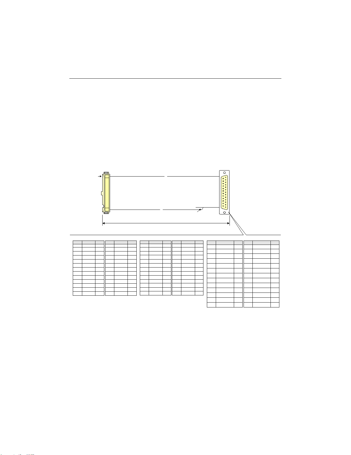
The PCI-936 provides a bi-directional parallel port, compatible with PC/XT, AT, PS/2,
EPP and ECP modes.
To date, only a few products can operate in EPP or ECP mode. To operate in EPP or ECP
mode, the peripheral must be designed to operate in this mode and the BIOS setup must be
configured to support it. The differences between the three modes appear in the pin
assignation.
42'', Parallel Port FlatCable
Female
26-pin Header
Pin 1
Parallel Port Pinout According to StandardMode
O
I
O
O
-
-
-
-
-
-
-
-
* Active low signal
AUTOFD*
ERROR*
INIT*
SELECTIN*
GND
GND
GND
GND
GND
GND
GND
GND
Pin # Pin # I/OSignalSignalI/O
14
1
15
16
17
18
19
20
21
22
23
24
25
STROBE*
2
D0
3
D1
4
D2
5
D3
6
D4
7
D5
8
D6
9
D7
10
ACK*
11
BUSY
12
PE
13
SELECT
Parallel Port Pinout According toEPP Mode
O
O
-
I/O
-
I/O
O
I/O
-
I/O
-
I/O
-
I/O
-
I/O
-
I/O
-
I
-
I
-
I
I
* Activelow signal
DATASTRB*
Not Used
Not Used
ADDRSTRB
GND
GND
GND
GND
GND
GND
GND
GND
Pin # Pin# I/OSignalSignalI/O
*
Cut Wire #26
42''
14
1
15
2
16
3
17
4
18
5
19
6
20
7
21
8
22
9
23
10
24
11
25
12
13
WRITE*
D0
D1
D2
D3
D4
D5
D6
D7
INTR
WAIT *
Not Used
Not Used
O
I/O
I/O
I/O
I/O
I/O
I/O
I/O
I/O
I
I
-
-
DB25 Female
Connector
13
25
14
1
Parallel Port Pinout Accord ing to ECP Mode
AUTOFD*
O
HOSTACK
FAULT*
I
PERIPHRQST*
INIT*
O
REVERS ERQST*
SELECTIN*
O
-
-
-
-
-
-
-
-
* Activelow signal
1
GND
GND
GND
GND
GND
GND
GND
GND
Pin #SignalI/O
2
2
1
2
Pin # I/OSignal
14
15
16
17
18
19
20
21
22
23
10
24
11
25
12
13
Compatible Mode
High Speed Mode
1
2
3
4
5
6
7
8
9
.
2
1
1, 2
STROBE*
D0
D1
D2
D3
D4
D5
D6
D7
ACK*
BUSY
PERIPHACK
PERROR
ACKREVERSE
SELECT
O
I/O
I/O
I/O
I/O
I/O
I/O
I/O
I/O
I
I
2
I
2
I
The parallel port connector (J10) is a male 26-pin header located at the top right side of the
board.
The following list includes approved vendors for the J10 connector’s mating parts:
Amp 746285-6 [optional strain relief: 499252-3],
Robinson Nugent IDS-C26PK-TG,
Thomas & Betts 622-2630 [optional strain relief: 622-2641].
(Polarized IDC female socket connector).
9-7
Page 56

PCI-936 Technical Reference Manual
9.3.1.1. Standard Mode
The Standard mode is a unidirectional parallel port. It is used for its compatibility with the
IBM PC standard.
9.3.1.2. EPP Mode
The EPP (Enhanced Parallel Port) mode consists of a hardware independent method of
accessing a parallel port configured as EPP. It provides support for single I/O cycle as well
as the high performance block I/O transfers. The EPP mode always uses the optimum
method for I/O transfers. For example, if the hardware supports it, EPP mode will perform
32-bit I/O block transfers.
EPP mode assumes that the parallel port can be used to connect more than one peripheral
device using Multiplexor or Daisy Chain configurations.
Multiplexor is an external device that permits up to eight parallel port devices to share a
single parallel port.
A Daisy Chain device has two ports: input and output. The input port is connected either to
the host parallel port or to the daisy chain device in front of it. The output is used to
connect the next peripheral device to the daisy chain. The last device, however, can be one
without daisy chain support.
9.3.1.3. ECP Mode
ECP (Extended Capabilities Port) works the same as EPP mode, but it will take precedence
over the EPP mode when addressing multiple logical devices in a single physical product.
While the EPP mode may intermix read and write operations without any overhead or
protocol handshaking, the ECP mode negotiates data transfers using a request from the host
and an acknowledgment from the peripheral.
✏✏✏✏
Note:
For more information on the ECP protocol, please refer to the Extended Capabilities
Port Protocol and ISA Interface Standard (available from Microsoft Corporation) or
contact our Technical Support department.
9-8
Page 57

10. INSTALLING ETHERNET
10.1. SETTING UP ETHERNET
10.1.1 CABLING
The PCI-936 Ethernet output may be set for 10Base-T or 100Base-T operation modes:
The 10Base-T interface uses UTP (Unshielded Twisted Pair) cables, category 5, 4 or 3 (5 is
better), while the 100Base-T cable must comply with the IEEE 802.3 10Base-T standard
for 2 pairs Category 5 UTP cable.
10.1.2 CONFIGURATION
The Ethernet controller on the PCI-936 resides on the PCI bus and is therefore Plug and Play
by default. No manual configuration is required. A diskette entitled “Network Drivers for
IN82557” is included with the Ethernet option. This diskette contains several operating system
network drivers.
To install the drivers, run the “setup.exe” program.
For other operating system drivers and installation instructions, contact Kontron’s Technical
Support department.
10-1
Page 58
PCI-936 Technical Reference Manual
10.2. ETHERNET CONNECTORS
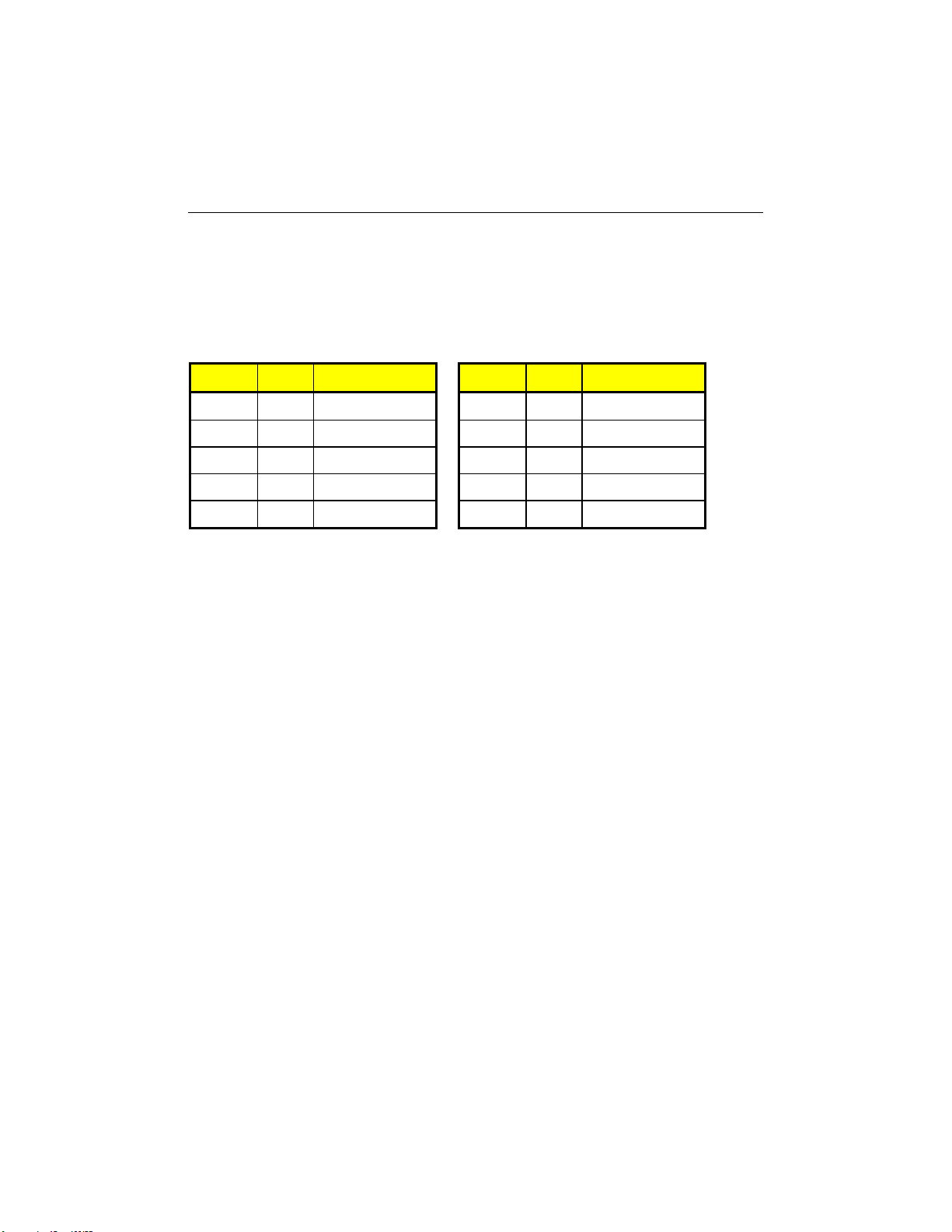
The pinout for the 10/100 Base-Tx connector appears in Table 10-1.
TABLE 10-1: Ethernet 10/100 Base-Tx RJ45 Connector (J18) – Pinout
Pin # I/O Signal Pin # I/O Signal
1OTD+ 2OTD-
3 I RD+ 4 - Not Connected
5 - Not Connected 6 I RD-
7 - Not Connected 8 - Not Connected
9 - CGND 10 - CGND
10.3. ETHERNET LEDs STATUS
The PCI-936 is equipped with two LEDs showing the transmission and reception status as
well as the link type. The LEDs can be seen on bracket when the Ethernet option is installed.
LED DS3 blinks when transmitting or receiving packets.
LED DS2 goes on when a 100-Base-Tx link is established. The LED is off when the link is at
10Mb per second.
10-2
Page 59

ONBOARD FEATURES
PAR
T
11. CONFIGURING DMA & IRQ
12. SETTING JUMPERS
13. POWERING UP THE SYSTEM
14. SOFTWARE SETUP
3
Page 60

Page 61

11. CONFIGURING DMA & IRQ
11.1. ALLOCATING DMA CHANNELS
The PCI-936 implements the functionality of two 8237 DMA controllers. Eight DMA
channels are available.
According to Plug and Play standards, the system BIOS automatically allocates DMA
Channel 1 or 3 for the ECP mode of the parallel port. Channel 2 is reserved for the floppy
controller and Channel 4 is used to cascade Channels 0 through 7 to the microprocessor.
The DMA Channel for the Plug and Play Ethernet device is automatically allocated by the
system BIOS among those available (Channels.
TABLE 11-1: DMA Channels
DMA 0 Available
DMA 1 PnP available (ECP)
DMA 2 Floppy controller
DMA 3 PnP available (ECP or Ethernet)
DMA 4 Cascade controller # 1
DMA 5 PnP available (Ethernet)
DMA 6 PnP available (Ethernet)
DMA 7 PnP available (Ethernet)
11-1
Page 62

PCI-936 Technical Reference Manual
11.2. ALLOCATING IRQ LINES
Two 8259 interrupt controllers handle the interrupts on the PCI-936 as follows:
ù Seven interrupt lines are directly linked to the keyboard controller, floppy controller,
timer, the real-time clock, both serial ports and the mouse.
ù The system BIOS automatically allocates IRQ5 or IRQ7 for the parallel port’s IRQ
line, depending on the settings in the AWARD BIOS Peripheral Setup’s Onboard
Parallel Port option: IRQ5 when the option is set to 278h or 3BCh; IRQ7 when set to
378h; IRQ5 or IRQ7 when set to Auto; when the option is set to Disabled, IRQ5 and
IRQ7 are available for onboard and external PCI/PnP devices, or for external non-PnP
devices (see note 1 below).
ù The primary and secondary IDE controllers are configured with the AWARD BIOS
Peripheral Setup screen’s Onboard IDE option: IRQ 14 is linked to primary IDE when
the option is set to Primary or Both; IRQ 15 is linked to secondary IDE when the
option is set to Secondary or Both; IRQ 14 and IRQ 15 are available for on
board/external PCI/PnP devices or external non-PnP devices (see note 1 below), when
the option is set to Disabled.
ù The on board PCI Ultra SCSI controller is automatically allocated an IRQ line by the
system BIOS among the available PCI/PnP IRQ lines.
ù The on board Plug and Play Ethernet is automatically allocated an IRQ line by the
system BIOS among the available PCI/PnP IRQ lines.
TABLE 11-2: IRQ Lines
Controller # 1 Controller # 2
IRQ 0 Timer 0 IRQ 8 Real-time clock
IRQ 1 Keyboard IRQ 9 Available
IRQ 2 Cascade controller # 2 IRQ 10 Available
IRQ 3 COM 2 * IRQ 11 Available
IRQ 4 COM 1 * IRQ 12 PS/2 Mouse Interface
IRQ 5 LPT2 * or available
IRQ 6 Floppy controller * IRQ 14 Primary IDE * or available
IRQ 7 LPT1 * or available
* All functions marked with an asterisk (*) can be disabled or reconfigured.
1
Available lines service on board and external PCI/PnP devices (when set to PCI/PnP in AWARD BIOS
PCI/PnP Setup screen) or an external non-PnP device (when set to ISA/EISA in AWARD BIOS PCI/PnP
Setup screen).
1
1
IRQ 13 Coprocessor Error
IRQ 15 Secondary IDE * or available
11-2
1
1
1
1
1
Page 63
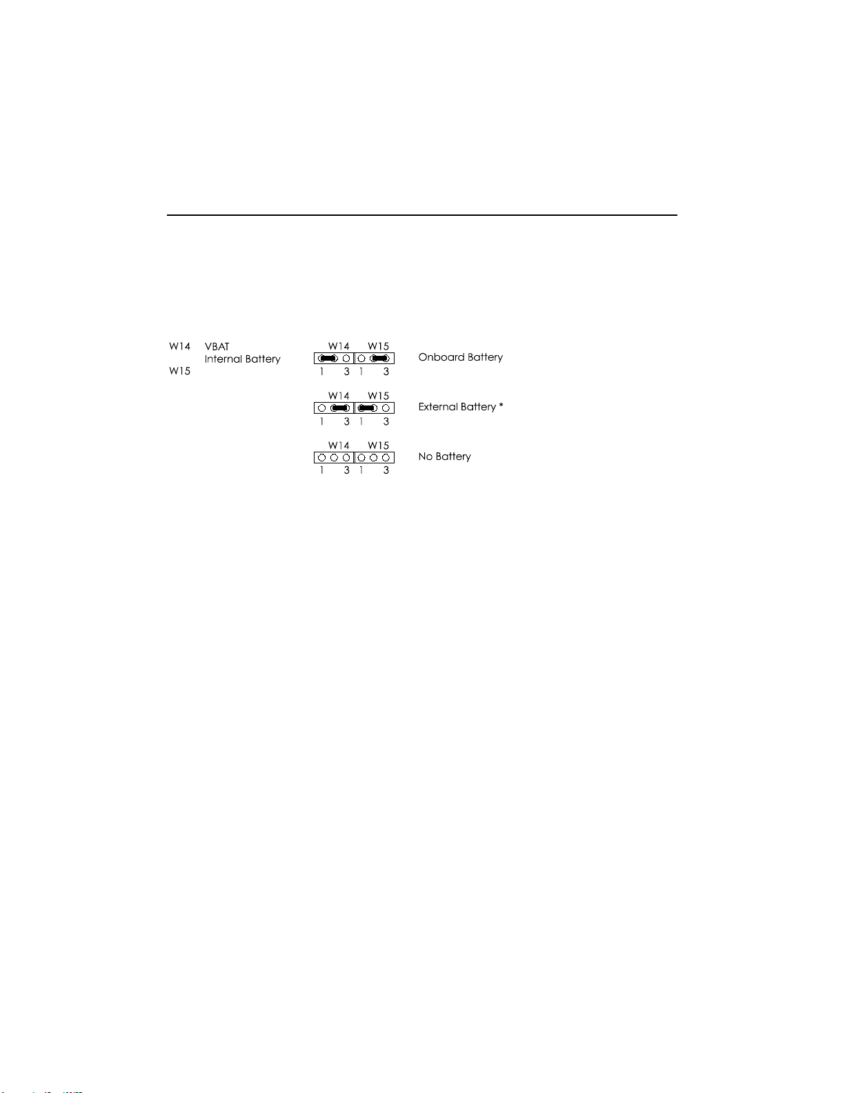
12. SETTING JUMPERS
12.1. CONNECTING THE BATTERY
Install jumpers W14 and W15 to enable the Internal Battery. This must be done to ensure your
CMOS settings are retained between power-ups.
Removing the W14 and W15 jumpers has the same effect as putting the battery in storage;
Kontron always ships its board with the battery jumper removed in order to increase the
life of the battery.
12.2. JUMPER SETTINGS
Tables 12-1 to 12-3 on the following pages show the PCI-936 jumpers and their initial setting.
These jumpers are labeled from W3 to W24, and J13.
12-1
Page 64
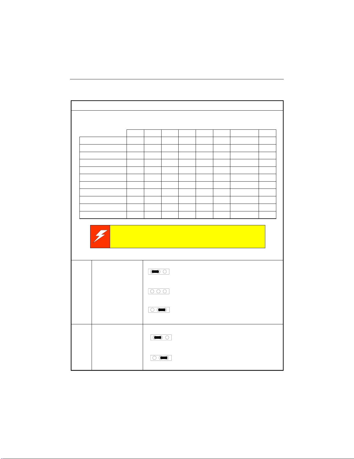
PCI-936 Technical Reference Manual
X
X
X
A
A
TABLE 12-1: Jumper Settings
NAME FUNCTION CONFIGURATION (INITIAL SETTING: * )
W3, W4, W6, W9, W10, W11, W21, W23 - CPU Type Selection
PENTIUM 100
PENTIUM 120
PENTIUM 133
PENTIUM 150
PENTIUM 166
PENTIUM 200
PENTIUM 166-MM
PENTIUM 200-MM
PENTIUM 233-MM
MD K6-166
MD K6-200
W5
SCSI Termination
W3
on
off
on
off
on
on
on
on
on
on
on
W4
off
on
on
on
on
off
on
off
off
on
off
W6
off
on
off
on
off
off
off
off
off
off
off
W9
off
off
off
on
on
on
on
on
off
on
on
W10
on
off
on
off
on
on
on
on
on
on
on
W11
on
off
on
off
on
on
on
on
on
on
on
W21
3-5 / 4-6
3-5 / 4-6
3-5 / 4-6
3-5 / 4-6
3-5 / 4-6
3-5 / 4-6
1-3 / 2-4
1-3/ 2-4
1-3/ 2-4
1-3/ 2-4
1-3/ 2-4
Careful attention should be taken when installing a processor:
Faultyjumper settings may definitely damage both your
processor and your board.
W5
13
W5
13
Controlled by software
Disabled by hardwa re
W23
3-5
3-5
3-5
3-5
3-5
3-5
4-6
4-6
4-6
2-4
2-4
W5
13
Controlled by hardware
(board is terminated) *
W12
Flat Panel
Clock Shift
W12
13
W12
13
Inverted
Normal *
12-2
Page 65
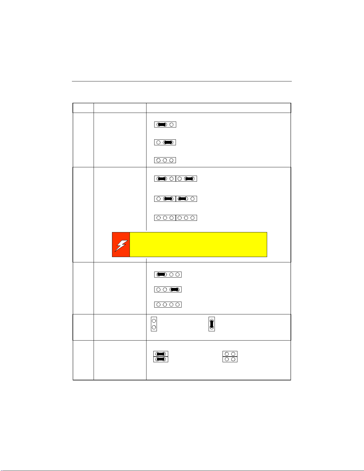
TABLE 12-2: Jumper Settings (Continued)
NAME FUNCTION CONFIGURATION (INITIAL SETTING: * )
Setting Jumpers
W13
W14
W15
W16
Watchdog Timer
VBAT
Internal Battery
Replace only with the same or equivalent type recommended
by the manufacturer. Dispose of used batteries according to the
manufacturer's instructions .
IOCHK Select
W13
13
W13
13
Dual-Stage Watchdog
Single-Stage Watchdog*
W13
1
W14
Watchdog Disabled
3
W15
Onboard Battery
1
W14
1
3
3
W15
External Battery *
1
W14
1
3
3
W15
No Battery
1
Danger of explosion if battery is incorrectly replaced.
14
14
14
W16
W16
W16
1
3
3
From Power Fail Output
From Watchdog Stage 1
Disabled *
J13
W17
W18
BIOS boot
selection
RS485 Termination
Setting
J13
Normal*
Emergency
J13
(boot block flash)
W17
W18
W17
W18
With Termination Without Termination *
12-3
Page 66
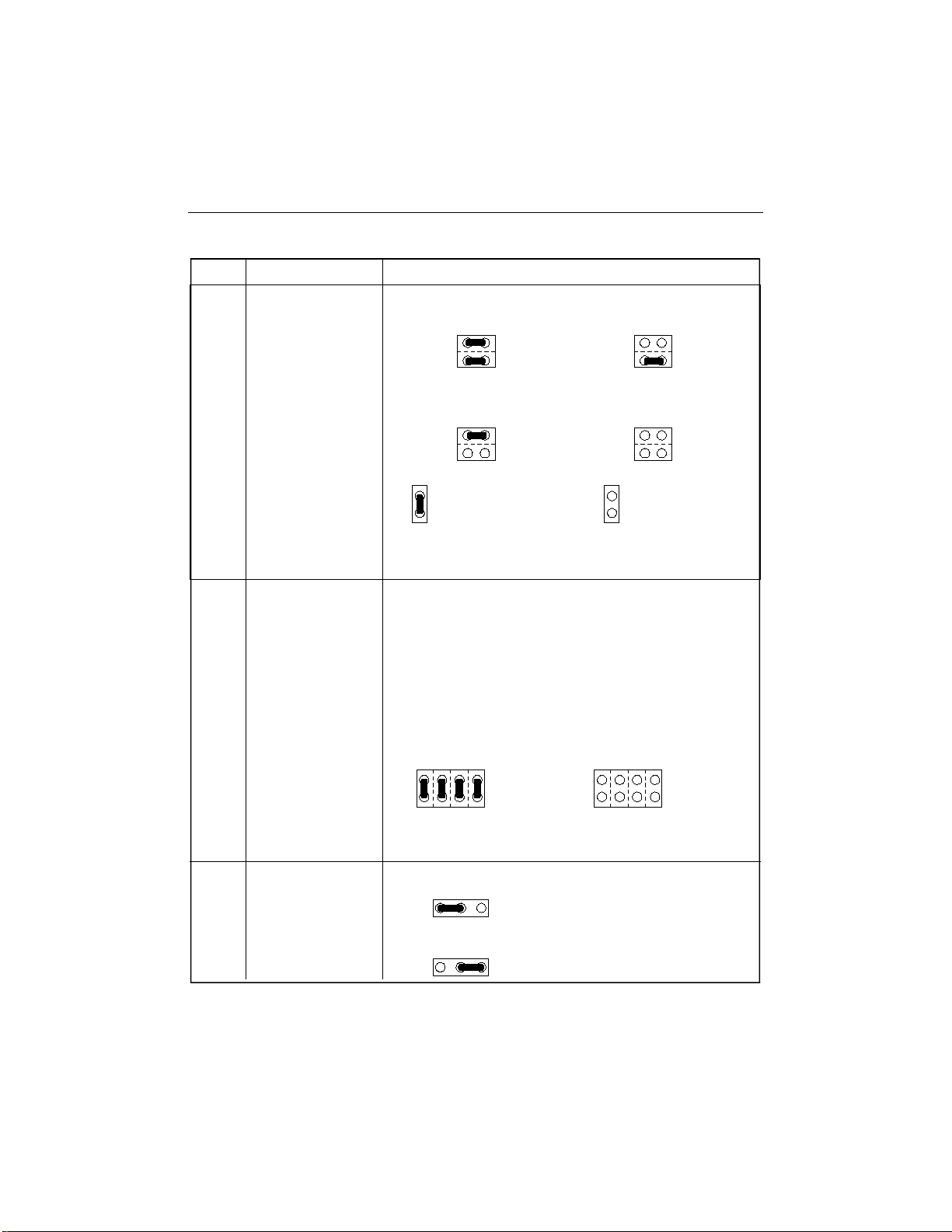
PCI-936 Technical Reference Manual
TABLE 12-3: Jumper Settings (Continued)
NAME FUNCTION CONFIGURATION (INITIAL SETTING: * )
W19
Supervisor I/O:
Base address
W20
Ethernet Enabling
W22
Extended BIOS
Modes
(These jumpers
are configured
separately, even
though they are
grouped together
here)
1
2
W19
W19
W20 W20
190H * 390H
4
3
1
2
4
3
W19
W19
1
2
4
3
1
2
4
3
Disabled Enabled *
1-2: Serial Download
1-2: Normal Mode *
Mode
3-4: VT100 Mode
5-6: Disable TEKNOR
Extension
7-8: Disable Onboard
VGA Controller
2
8
W22 W22
3-4: Standard Mode *
5-6: Enable TEKNOR
Extension *
7-8: Enable Onboard
VGA Controller *
2
8
390H290H
W24
Flat Panel
Power Selection
W24
W24
7
12-4
3
3.3 volt selection
3
5 volt selection*
1
1
1
1
7
Page 67
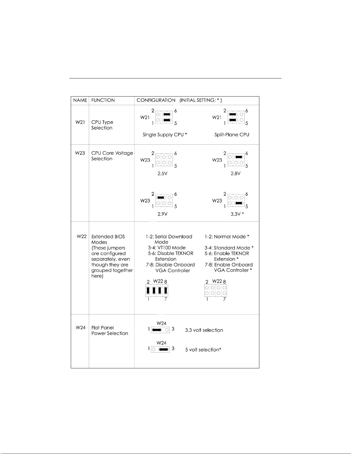
TABLE 12-4: Jumper Settings: W17-W20
Setting Jumpers
12-5
Page 68
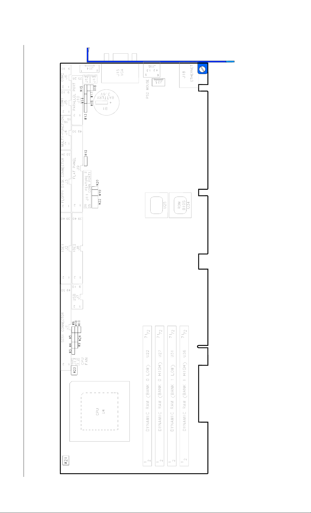
12-6
PCI-936 Technical Reference Manual
JUMPER LOCATION
Page 69

13. POWERING UP THE SYSTEM
13.1. Connecting Power Supply (J14)
Power can be drawn on the PCI-936 using on-board 6-pin power connector (J14).
TABLE 13-1: Power Connector (J14) pinout
Pin number Signal
1VCC
2GND
3GND
4+12
5GND
6VCC
13.2. Powering Up
You are now ready to power up your system.
1. Insert a bootable diskette in drive A to start your system with DOS.
2. Hit the DELETE key before or when this message appears near the bottom of the screen:
″Press DEL to enter SETUP″. The main menu appears on the screen.
- In Standard Setup, set the date and time.
- In other menu choices, set other options (if necessary).
3. From the main menu, press the F10 key. Type “Y” to save your setup. The system will
continue the boot procedure.
4. Once the boot procedure is completed, reboot the system to make sure everything works
properly.
13-1
Page 70

PCI-936 Technical Reference Manual
13.3. Troubleshooting
If you should encounter a problem, verify the following items:
• Make sure that all connectors are connected properly. On the standard flat ribbon cable
used for the floppy connector, pin 1 is indicated by small red stripe. Verify that this red
stripe is located on the appropriate side of the connector.
• Verify your boot diskette. It must be a system disk and it must be in proper working order.
• If the system still does not start up properly, you should try booting your system with only
the power cord and video monitor connected to the board (this is the minimum required to
see if the board is working).
• If you still are not able to get your board up and running, contact our Technical Support
department for assistance.
13-2
Page 71

14. SOFTWARE SETUP
14.1. THE AWARD SETUP PROGRAM
14.1.1 ACCESSING THE AWARD SETUP PROGRAM
The PCI-936 uses the AWARD Setup program, a setup utility in EEPROM that is accessed by
pressing the DELETE key at the appropriate time during system boot. This utility is used to set
configuration data in CMOS RAM.
CAUTION
Before modifying CMOS setup parameters, insure that the W14 and W15 Battery
Selection jumpers are installed to enable the CMOS backup.
(See section 12, “Setting Jumpers”)
To run the AWARD Setup program incorporated in the ROM BIOS:
1. Turn on or reboot the system.
2. Hit the DELETE key before or when the message - "PRESS DEL TO ENTER SETUP"
appears near the bottom of the screen.
3. The main menu appears on the screen.
14-1
Page 72

PCI-936 Technical Reference Manual
The actual menu screen appears below:
STANDARD CMOS SETUP
BIOS FEATURES SETUP
CHIPSET FEATURES SETUP
POWER MANAGEMENT SETUP
PNP/PCI CONFIGURATION
LOAD BIOS DEFAULTS
LOAD SETUP DEFAULTS
Esc : Quit
F10 : Save & Exit Setup
Time, Date, Hard Disk Type...
ROM PCI/ISA BIOS
CMOS SETUP UTILITY
AWARD SOFTWARE, INC.
INTEGRATED PERIPHERALS
SUPERVISOR PASSWORD
USER PASSWORD
PASSWORD SETTING
IDE HDD AUTO DETECTION
4DD LOW LEVEL FORMAT
SAVE & EXIT SETUP
EXIT WITHOUT SAVING
↑↓→← : Select Item
(Shift)F2 : Change Color
14-2
Page 73

Software Setup
14.1.2 USING AWARD SETUP
The arrow keys (↑ ↓ → ←) are used to highlight items on the menu and the PageUp and
PageDown keys are used to change the entry values for the highlighted item. To select an
entry, press the Enter key. Also, you can press the F1 key to obtain help information or the Esc
key to leave an option, close a menu or to quit the program.
Table 14-1 provides more details on how to navigate in the Setup program:
TABLE 14-1
Up arrow (↑)
Down arrow (↓)
Left arrow (←)
Right arrow (→)
Esc key In Main Menu: Quit settings (Answer ‘Y’ to save changes into CMOS).
PgUp key Increase the numeric value or make changes.
PgDn key Decrease the numeric value or make changes.
+ key Increase the numeric value or make changes.
- key Decrease the numeric value or make changes.
F1 key General help.
F2 and
Shift F2 keys
F4 key Reserved.
F5 key In sub-menu: Restore the previous setup values from BIOS Default
F6 key In sub-menu: Load the default setup values from BIOS Default Table.
F7 key In sub-menu: Load the setup values from the Setup Default Table .
F8 key Reserved.
F9 key Reserved.
F10 key When in Main Menu: Save all the CMOS changes.
Move to previous item.
Move to next item.
Move to the item in the left hand.
Move to the item in the right hand.
In sub-menus: Exit and return to Main Menu.
Change color from total 16 colors: F2 to select color forward, Shift F2
to select color backward.
Table.
14-3
Page 74

PCI-936 Technical Reference Manual
The Main Menu includes the following categories:
Standard CMOS
Setup
BIOS Features
Setup
Chipset Features
Setup
Power Management
Setup
PnP/PCI
Configuration
Integrated
Peripherals
Supervisor/User
Password Setting
IDE HDD Auto
Detection
HDD Low Level
Format
This Setup page includes all the items in a standard, ATcompatible BIOS.
This Setup page includes all the items of AWARD’s special
enhanced features.
This Setup page includes all the items of the chipset’s special
features.
This Setup page sets power conservation options.
This Setup page sets Plug and Play and PCI Local Bus
configuration options.
I/O subsystems that depend on the integrated peripherals
controller in your system.
Change, set, or disable password. It allows you to limit access to
the system and the Setup, or just to the Setup.
Automatically detect and configure hard disk parameters. This
ability is included in the event you are uncertain of your hard
disk’s parameters.
This option does not appear in many BIOS versions. Most
manufacturers of IDE hard drives strongly recommend that you do
not run a low-level format on their drives, because of the danger
that the bad-track table may be over-written. Award supplies this
utility for service personnel only.
If you feel you need to run a low-level format on your hard
drive, contact your drive manufacturer for instructions!
Load Bios
Defaults
Load Setup
Defaults
The BIOS defaults represent settings that provide the minimum
requirements for your system to operate.
The chipset defaults are settings that provide for maximum system
performance.
14-4
Page 75

14.1.3 SAVING CONFIGURATIONS & EXITING AWARD SETUP
Use one of the following options available from the Main Menu:
Software Setup
Save & Exit
Exit Without
Saving
After having modified the AWARD Setup, you can save the
configuration in CMOS RAM, by selecting this option. This
option will not change the values saved in Flash EPROM. To
update the values in Flash, enter the VIP-UP program and perform
a save (F10).
This option is used to exit AWARD Setup without saving the
configuration to CMOS RAM.
14-5
Page 76

PCI-936 Technical Reference Manual
14.1.4 STANDARD CMOS SETUP
This part of the setup allows you to set the time, date, hard disk type, types of floppy drives
and video type.
Date/Time
Hard Disks
Drive A / Drive B
Video
Halt on
Memory
The current values for each category are displayed. Enter new
values through the keyboard.
Two IDE controllers are defined on the PCI-936 board (Primary
and Secondary), each can have two disks: Master Disk (bootable)
or Slave Disk.
Select the category identifying the types of floppy disk drive A or
drive B that have been installed in the computer.
This option specifies the basic type of display adapter card
installed in the system.
This option specifies the type of errors that will stop the system
during the BIOS booting procedure. The settings are All errors,
No errors, All but keyboard (default setting), All but diskette and
All but disk/key.
This display-only option summarizes the amount of Base,
Extended and other types of memory installed in the system.
14-6
Page 77

Software Setup
14.1.5 BIOS FEATURES SETUP
This part of the setup handles options and features such as boot sequence, NUM LOCK,
security options, shadowing, ...
Whenever you are not sure about a certain setting, you may refer to the list of default values.
The list of defaults is provided in the event that a value has been changed and one wishes to
set this option to its original value. Loading the BIOS or SETUP defaults will affect all the
options and will reset options previously altered.
The BIOS default settings consist of the safest set of parameters. Use them if the system is
behaving erratically. They should always work but do not provide optimal system
performance.
The SETUP default values provide optimum performance settings for all devices and system
features.
14-7
Page 78

table of the hard disk drive. You should then run an anti-virus program. Keep in mind that this feature protects only the boot sector, not
the entire hard drive.
Note: Many disk diagnostic programs that access the boot sector table can trigger the virus-warning message. If you plan to
run such a program, we recommend that you first disable the virus warning.
recommend that you normally disable quick POST. It is better to find a problem during POST than lose data during your work.
The original IBM PCs load the DOS operating system from drive A (floppy disks), so IBM PC-compatible systems are designed to
search for an operating system first on drive A, then on drive C (hard disk). However, modern computers usually load the operating
system from the hard drive, and may even load it from a CD-ROM drive.
drive A to logical drive B.
(CDROM, C, A) ; (C)
40 tracks; drives with 720KB, 1.2MB, and 1.44MB capacity all have 80 tracks. Because very few modern PCs have 40 track floppy
drives, we recommend that you set this field to “Disabled” to save time.
generates numbers instead of controlling cursor operations.
(such as old games) may require a slow CPU speed. The default setting is High.
by the keyboard controller in your system. When Enabled, you can select a typematic rate and a typematic delay.
When the typematic rate setting is Enabled, you can select a typematic rate (the rate at which characters repeat when you hold down a
key) of 6, 8, 10, 12, 15, 20, 24 or 30 characters per second.
500, 750 or 1000 milliseconds.
per second
DRAM bus.
Firmware not shadowed must be read by the system through the 8-bit X-bus. Shadowing improves the performance of the system
BIOS and similar firmware for expansion peripherals, but it also reduces the amount of high memory (640KB to 1MB) available for
loading device drivers, etc. Enable shadowing into each section of memory separately. Many system designers hardwire shadowing of
the system BIOS and eliminate a System BIOS Shadow option.
occupied by other expansion card firmware. If an expansion peripheral in your system contains ROM-based firmware, you need to
know the address range the ROM occupies to shadow it into the correct area of RAM.
14-8
Option BIOS Defaults Setup Defaults Possible Settings Description
TABLE 14-2: BIOS Features Setup
Virus Warning Disabled Disabled Enabled, Disabled When Enabled, you receive a warning message if a program (specifically, a virus) attempts to write to the boot sector or the partition
CPU Internal Cache Enabled Enabled Enabled, Disabled Enables or Disables the CPU Internal Cache.
CPU External Cache Disabled Enabled Enabled, Disabled Enables or Disables the CPU external Cache.
Quick Power On Self Test Disabled Disabled Enabled, Disabled Select Enabled to reduce the amount of time required to run the power-on self-test (POST). A quick POST skips certain steps. We
Boot Sequence A, C A, C (A,C) ; (C,A) ; (C, CDROM, A) ;
Swap Floppy Drive Disabled Disabled Enabled, Disabled This field is effective only in systems with two floppy drives. Selecting Enabled assigns physical drive B to logical drive A, and physical
Boot Up Floppy Seek Disabled Disabled Enabled, Disabled When Enabled, the BIOS tests (seeks) floppy drives to determine whether they have 40 or 80 tracks. Only 360KB floppy drives have
Boot Up NumLock Status Off Off On, Off Toggle between On or Off to control the state of the NumLock key when the system boots. W hen toggled On, the numeric keypad
Boot Up System Speed High High Low, High Select High to boot at the default CPU speed; select Low to boot at the speed of the AT bus. Some add-in peripherals or old software
Typematic Rate Setting Disabled Disabled Enabled, Disabled When Disabled, the following two items (Typematic Rate and Typematic Delay) are irrelevant. Keystrokes repeat at a rate determined
Typematic Rate (Chars/Sec) 6 6 6, 8, 10, 12, 15, 20, 24, 30 characters
Typematic Delay (Msec) 250 250 250, 500, 750, 1000 milliseconds When the typematic rate setting is Enabled, you can select a typematic delay (the delay before keystrokes begin to repeat) of 250,
Security Option Setup Setup Setup, System If you have set a password, select whether the password is required every time the system boots, or only when you enter Setup.
OS Select For DRAM>64MB Non-OS2 Non-OS2 Non-OS/2, OS/2 Select OS2 only if you are running an OS/2 operating system with greater than 64MB of RAM.
Video BIOS Shadow Enabled Enabled Enabled, Disabled Software that resides in a read-only memory (ROM) chip on a device called firmware. The Award BIOS allows shadowing of firmware
CC000-CFFFF Shadow Disabled Disabled Enabled, Disabled such as the system BIOS, video BIOS, and similar operating instructions that come with some expansion peripherals (for example, a
D0000-D3FFF Shadow Disabled Disabled Enabled, Disabled SCSI adapter). Shadowing copies of firmware from ROM into system RAM, where the CPU can read it through the 16-bit or 32-bit
D4000-D7FFF Shadow Disabled Disabled Enabled, Disabled
D8000-DBFFF Shadow Disabled Disabled Enabled, Disabled
DC000-DFFFF Shadow Disabled Disabled Enabled, Disabled Video BIOS shadows into memory area C0000-CBFFF. The remaining areas shown on the BIOS Features Setup screen may be
Page 79

Software Setup
14.1.6 CHIPSET FEATURES SETUP
This part of the setup allows you to define chipset-specific options and features.
Whenever you are not sure about a certain setting, you may refer to the list of default values.
The list of defaults is provided in the event that a value has been changed and one wishes to
set this option to its original value. Loading the BIOS or SETUP defaults will affect all the
options and will reset options previously altered.
The BIOS default settings consist of the safest set of parameters. Use them if the system is
behaving erratically. They should always work but do not provide optimal system
performance.
The SETUP default values provide optimum performance settings for all devices and system
features.
CAUTION
These parameters have been provided to give control over the system. However, the
values for these options should be changed only if the user has a full understanding of
the timing relationships involved.
14-9
Page 80

information stored in CMOS. Many fields in this screen are not available when Auto Configuration is Enabled.
factory setting unless you install new memory that has a different performance rating than the original DRAMs.
transition from RAS to Column Address Strobe (CAS).
faster the system addresses memory. Selecting timing numbers lower than the installed DRAM is able to support can result in memory
errors.
refreshed. If insufficient time is allowed, refresh may be incomplete and data lost.
value from the setting determined by the board designer for the installed DRAM might cause memory errors.
numbers lower than the installed DRAM is able to support can result in memory errors.
Leadoff lets the DRAM controller pass the read command to memory slightly before it has fully decoded the address, thus speeding up
the read process.
any program writes to this memory area, a system error may occur.
any program writes to this memory area, a system error may occur.
the PCI bus is so much faster than the ISA bus.
These two fields let you add recovery time (in bus clock cycles) for 16-bit and 8-bit I/O.
current cycle are complete, resulting in faster performance.
access to local DRAM.
with PCI specifications version 2.1.
select Fast (3-1-1-1, 2-1-1-1) or Faster (3-1-1-1, 1-1-1-1). Cache timing 3-1-1-1 is at the CPU access speed. It requires special SRAMs
because the 3-1-1-1 timing is at the CPU clock rate.
information of peripherals that need to use this area of system memory usually discusses their memory requirements.
14-10
Option BIOS Defaults Setup Defaults Possible Settings Description
TABLE 14-3: Chipset Setup
Auto Configuration Enabled Enabled Enabled, Disabled Auto Configuration selects predetermined optimal values of chipset parameters. When Disabled, chipset parameters revert to setup
DRAM Timing 70 ns 70ns 70 ns, 60ns The value in this field depends on performance parameters of the installed memory chips (DRAM). Do not change the value from the
DRAM RAS# Precharge Time 4 4 4, 3 Select the number of CPU clocks allocated for the Row Address Strobe (RAS#) signal to accumulate its charge before the DRAM is
DRAM R/W Leadoff Timing 7/6 7/6 7/6, 6/5 Select the combination of CPU clocks the DRAM on your board requires before each read from or write to the memory. Changing the
RAS to CAS Delay 3 3 3, 2 When DRAM is refreshed, both rows and columns are addressed separately. This setup item allows you to determine the timing of the
DRAM Read Burst (EDO/FPM) x444/x444 x444/x444 x444/x444, x333/x444, x222/x333 Sets the timing for reads from EDO (Extended Data Output) or FPM (Fast Page Mode) memory. The lower the timing numbers, the
DRAM Write Burst Timing x444 x444 x444, x333, x222 Sets the timing for writes to memory. The lower the timing numbers, the faster the system addresses memory. Selecting timing
Turbo Read Leadoff Disabled Disabled Enabled, Disabled Select Enabled to shorten the leadoff cycles and optimize performance in cacheless, 50-60 MHz, or one-bank EDO DRAM systems.
DRAM Speculative Leadoff Disabled Disabled Enabled, Disabled A read request from the CPU to the DRAM controller includes the memory address of the desired data. When Enabled, Speculative
Turn-Around Insertion Disabled Disabled Enabled, Disabled When Enabled, the chipset inserts one extra clock to the turn-around of back-to-back DRAM cycles.
ISA Clock PCI CLK/4 PCI CLK/4 PCI CLK/4, PCI CLK/3 You can set the speed of the AT bus at one-third or one-fourth of the CPU clock speed.
System BIOS Cacheable Disabled Enabled Enabled, Disabled Selecting Enabled allows caching of the system BIOS ROM at F0000h-FFFFFh, resulting in better system performance. However, if
Video BIOS Cacheable Disabled Enabled Enabled, Disabled Selecting Enabled allows caching of the video BIOS ROM at C0000h to C7FFFh, resulting in better video performance. However, in
8/16 Bit I/O Recovery Time 3 1 1, 2, 3, 4, 5, 6, 7, 8, NA The I/O recovery mechanism adds bus clock cycles between PCI-originated I/O cycles to the ISA bus. This delay takes place because
16 Bit I/O Receiving Time 2 1 1, 2, 3, 4, NA
Peer Concurrency Enabled Enabled Enabled, Disabled Peer concurrency means that more than one PCI device can be active at a time.
Chipset Special Features Disabled Enabled Enabled, Disabled When Disabled, the chipset behaves as if it were the earlier Intel 82430FX chipset.
DRAM ECC/PARITY Select Parity Parity ECC, Parity Set this option according to the type of DRAM installed in your system: error-correcting code (ECC) or parity (default).
Memory Parity/ECC Check Auto Auto Enabled, Disabled, Auto In Auto mode, the BIOS enables memory checking automatically when it detects the presence of ECC or parity DRAM.
Single Bit Error Report Enabled Enabled Enabled, Disabled If ECC is enabled, selecting Enabled here tells the system to report an error when a correctable single-bit error occurs.
L2 Cache Cacheable Size 64MB 64MB 64MB, 512MB Select 512MB only if your system RAM is greater than 64MB.
Chipset NA# Asserted Enabled Enabled Enabled, Disabled Selecting Enabled allows pipelining, in which the chipset signals the CPU for a new memory address before all data transfers for the
Pipeline Cache Timing Faster Faster Faster, Fastest For a secondary cache of 256KB (one bank), select Faster. For a secondary cache of 512KB (two banks), the system designer must
Passive Release Enabled Enabled Enabled, Disabled When Enabled, CPU to PCI bus accesses are allowed during passive release otherwise the arbiter only accepts another PCI master
Delayed Transaction Disabled Disabled Enabled, Disabled The chipset has an embedded 32-bit posted write buffer to support delay transactions cycles. Select Enabled to support compliance
Memory Hole Location None None 512K-640K, 15M-16M You can reserve this area of system memory for ISA adapter ROM. When this area is reserved, it cannot be cached. The user
TEKNOR Base Port Location 190h 190h 190h, 290h, 390h This parameter must reflect the jumper settings for TEKNOR I/O Base Port.
Page 81

Software Setup
14.1.7 POWER MANAGEMENT SETUP
This part of the setup sets power conservation options.
Whenever you are not sure about a certain setting, you may refer to the list of default values.
The list of defaults is provided in the event that a value has been changed and one wishes to
set this option to its original value. Loading the BIOS or SETUP defaults will affect all the
options and will reset options previously altered.
The BIOS default settings consist of the safest set of parameters. Use them if the system is
behaving erratically. They should always work but do not provide optimal system
performance.
The SETUP default values provide optimum performance settings for all devices and system
features.
14-11
Page 82

This option allows you to select the type (or degree) of power saving for Doze, Standby, and Suspend modes.
Max Saving: Maximum power savings. Only available for SL CPUs. Inactivity period is 1 minute in each mode.
Min Saving: Minimum power savings. Inactivity period is 1 hour in each mode (except the hard drive).
Define, Disabled
Electronics Standards Association (VESA). Use the software supplied for your video subsystem to select video management
values.
14-12
User Define: Set each mode individually. Select time-out periods in the PM Timers section (see below).
Determines the manner in which the monitor is blanked.
V/H SYNC + Blank: System turns off vertical and horizontal synchronization ports and writes blanks to the video buffer.
DPMS Support: Select this option if your monitor supports the Display Power Management Signaling (DPMS) standard of the Video
Blank Screen: System only writes blanks to the video buffer.
Screen
system.
After the selected period of system inactivity (1 minute to 1 hour), the CPU clock runs at lower speed while all other devices still operate at
full speed.
1 hour, Disabled
After the selected period of system inactivity (1 minute to 1 hour), the fixed disk drive and the video shut off while all other devices still
operate at full speed.
1 hour, Disabled
After the selected period of system inactivity (1 minute to 1 hour), all devices except the CPU shut off.
1 hour, Disabled
up the system.
The default wake-up event is keyboard activity. In these wake-up event fields, you can turn On or Off four commonly used interrupts. For
example, if you have a modem on IRQ3, you can turn on IRQ3 as a wake-up event, so an interrupt from the modem can wake up the
system. Or you may wish to turn Off IRQ12 (the PS/2) mouse as a wake-up event, so accidentally brushing the mouse does not awaken the
system.
Option BIOS Defaults Setup Defaults Possible Settings Description
Power Management Disabled Disabled Min Saving, Max Saving, User
TABLE 14-4: Power Management Setup
PM Control by APM Yes Yes Yes, No If Advanced Power Management (APM) is installed on your system, selecting Yes gives better power savings.
Video Off Method Disabled Disabled V/H SYNC + Blank, DPMS, Blank
Modem Use IRQ NA NA NA, 3, 4, 5, 7, 9, 10, 11 Name the interrupt request (IRQ) line assigned to the modem (if any) on your system. Activity of the selected IRQ always awakens the
PM Timers The following modes are Green PC power saving functions. They are user-configurable only during User Defined Power Management mode.
Doze Mode Disabled Disabled 1, 2, 4, 6, 8, 10, 20, 30, 40 mins,
Standby Mode Disabled Disabled 1, 2, 4, 6, 8, 10, 20, 30, 40 mins,
Suspend Mode Disabled Disabled 1, 2, 4, 6, 8, 10, 20, 30, 40 mins,
HDD Power Down Disabled Disabled 1, 2, 3, (...), 15 mins After the selected period of drive inactivity (1 to 15 min), the hard disk drive powers down while all other devices remain active.
Wake Up Events On, Off When the system is in Doze or Standby mode, you may disable activity monitoring of some common interrupt requests so they do not wake
IRQ3 Off On
IRQ4 Off On
IRQ8 Off On
IRQ12 Off On
Power Down and Resume Events Off On On, Off You may disable monitoring of common interrupt requests so they do not reset activity timers.
IRQ3 (COM 2) Off On
IRQ 4 (COM 1) Off On
IRQ 5 (LPT2) Off On
IRQ 6 (Floppy Disk) Off Off
IRQ 7 (LPT 1) Off On
IRQ 8 (RTC Alarm) Off Off
IRQ 9 (IRQ 2 Redir) Off On
IRQ 10 (Reserved) Off On
IRQ 11 (Reserved) Off On
IRQ12 (PS/2 Mouse) Off On
IRQ 13 (Coprocessor) Off On
IRQ 14 (Hard Disk) Off On
IRQ 15 (Reserved) Off On
Page 83

Software Setup
14.1.8 PnP/PCI SETUP
This part of the setup sets PnP/PCI options.
Whenever you are not sure about a certain setting, you may refer to the list of default values.
The list of defaults is provided in the event that a value has been changed and one wishes to
set this option to its original value. Loading the BIOS or SETUP defaults will affect all the
options and will reset options previously altered.
The BIOS default settings consist of the safest set of parameters. Use them if the system is
behaving erratically. They should always work but do not provide optimal system
performance.
The SETUP default values provide optimum performance settings for all devices and
system features.
14-13
Page 84

# A. Assigning INT# B has no meaning unless the peripheral device requires two interrupt services rather
# fields default to values appropriate for two PCI IDE channels, with the primary PCI IDE channel having a lower
using the interrupt:
Legacy ISA Devices compliant with the original PC AT bus specification, requiring a specific interrupt (such as IRQ4 for serial port 1).
the interrupt requests (IRQs) and DMA assignment fields disappear, as the BIOS automatically assigns them.
you have installed a new add-on and the system reconfiguration has caused such a serious conflict that the operating system cannot
boot.
PCI/ISA PnP Devices compliant with the Plug and Play standard, whether designed for PCI or ISA bus architecture.
device using the interrupt:
Legacy ISA Devices compliant with the original PC AT bus specification, requiring a specific DMA channel.
PCI/ISA PnP Devices compliant with the Plug and Play standard, whether designed for PCI or ISA bus architecture.
connection is assigned INT
than just one. Because the PCI IDE interface in the chipset has two channels, it requires two interrupt services. The primary and
This field lets you select PCI IDE IRQ mapping or PC AT (ISA) interrupts. If your system does not have one or two PCI IDE connectors
on the system board, select values according to the type of IDE interface(s) installed in your system (PCI or ISA). Standard ISA
interrupts for IDE channels are IRQ14 for primary and IRQ15 for secondary.
secondary IDE INT
Select a base address for the memory area used by any peripheral that requires high memory.
interrupt than the secondary.
14-14
DC00
PCI-SLOT3, PCI-SLOT4
Option BIOS Defaults Setup Defaults Possible Settings Description
TABLE 14-5: PnP/PCI Setup
Resources Controlled By Auto Manual Auto, Manual The Award Plug and Play BIOS can automatically configure all the boot and Plug and Play-compatible devices. If you select Auto, all
Reset Configuration Data Disabled Disabled Enabled, Disabled Normally, you leave this field Disabled. Select Enabled to reset Extended System Configuration Data (ESCD) when you exit Setup if
IRQ n Assigned To PCI/ISA PnP, Legacy ISA When resources are controlled manually, assign each system interrupt as one of the following types, depending on the type of device
DMA n Assigned To PCI/ISA PnP, Legacy ISA When resources are controlled manually, assign each system DMA channel as one of the following types, depending on the type of
PCI IRQ Activated By Level Level Level, Edge Leave the IRQ trigger set at Level unless the PCI device assigned to the interrupt specifies Edge-triggered interrupts.
PCI IDE IRQ Map To PCI-Auto PCI-Auto PCI-Auto, ISA, PCI-SLOT1, PCI-SLOT2,
Primary IDE INT# A A A, B, C, D Each PCI peripheral connection is capable of activating up to four interrupts: INT# A, INT# B, INT# C and INT# D. By default, a PCI
Secondary IDE INT# B B A, B, C, D
Used Mem Base Address NA NA NA, C800, CC00, D000, D400, D800,
Used Mem Length - - -, 8K, 16K, 32K, 64K Select a length for the memory area specified in the previous field. This field does not appear if no base address is specified.
Page 85

Software Setup
14.1.9 INTEGRATED PERIPHERALS SETUP
This part of the setup sets Integrated Peripherals options.
Whenever you are not sure about a certain setting, you may refer to the list of default values.
The list of defaults is provided in the event that a value has been changed and one wishes to
set this option to its original value. Loading the BIOS or SETUP defaults will affect all the
options and will reset options previously altered.
The BIOS default settings consist of the safest set of parameters. Use them if the system is
behaving erratically. They should always work but do not provide optimal system
performance.
✏✏✏✏
NOTE
The SETUP default values provide optimum performance settings for all devices and
system features.
14-15
Page 86

(most new drives do), select Enabled for automatic detection of the optimal number of block read/writes per sector the drive can
support.
channel separately.
The four IDE PIO (Programmed Input/Output) fields let you set a PIO mode (0-4) for each of the four IDE devices that the onboard IDE
interface supports. Modes 0 through 4 provide successively increased performance. In Auto mode, the system automatically
determines the best mode for each device.
add-in FDC or the system has no floppy drive, select Disabled in this field.
Select a logical COM port name and matching address for the first and second serial ports.
Select a logical LPT port name and matching address for the physical parallel (printer) port.
Select an operating mode for the onboard parallel port. Select ECP or EPP unless you are certain both your hardware and software
does not support EPP or ECP mode.
14-16
Mode 4, Auto
0 Auto Mode 0, Mode 1, Mode 2, Mode 3,
Option BIOS Defaults Setup Defaults Possible Settings Description
Disabled
3E8/IRQ4, 2E8/IRQ3, Auto
ECP+EPP1.7, SPP, EPP1.9+SPP, ECP
TABLE 14-6: Integrated Peripherals Setup
IDE HDD Block Mode Disabled Enabled Enabled, Disabled Block mode is also called block transfer, multiple commands, or multiple sector read/write. If your IDE hard drive supports block mode
PCI Slot IDE 2nd Channel Enabled Enabled Enabled, Disabled You may separately disable the second channel on an IDE interface installed in a PCI expansion slot.
On-Chip Primary/Secondary PCI IDE Enabled Enabled Enabled, Disabled The integrated peripheral controller contains an IDE interface with support for two IDE channels. Select Enabled to activate each
IDE Primary/Secondary Master/Slave
PIO
USB Controller Enabled Enabled Enabled, Disabled Select Enabled if your system contains a Universal Serial Bus (USB) controller and you have USB peripherals.
Onboard FDC Controller Enabled Enabled Enabled, Disabled Select Enabled if your system has a floppy disk controller (FDC) installed on the system board and you wish to use it. If you install an
Onboard Serial Port 1/2 Auto Auto Disabled, 3F8/IRQ4, 2F8/IRQ3,
Onboard Parallel Port 378/IRQ7 378/IRQ7 378/IRQ7, 278/IRQ5, 3BC/IRQ7,
Parallel Port Mode ECP+EPP 1.9 ECP+EPP1.9 ECP+EPP1.9, Normal, EPP1.7+SPP,
ECP Mode Use DMA 3 3 1, 3 Select a DMA channel for the port.
Page 87

Software Setup
14.2. THE VIP-UP PROGRAM
14.2.1 ACCESSING THE VIP-UP PROGRAM
The VIP-UP program is Kontron's own Setup program for enabling / disabling / relocating
various hardware features on the PCI-936.
During boot-up, hit the CTRL and V keys simultaneously, before or when you see the message
"Press CTRL-V to enter Kontron VIP-UP" at the top of the screen (CTRL-V will work,
even if the message display is disabled in VIP-UP).
At the DOS prompt, type "VIP-UP" and press ENTER. This program is available on the
utility disk.
There are two screens in the VIP-UP program. The values appearing on the right side of each
screen can be modified. Follow the instructions found at the bottom of the screen to select
another value.
Use the ↑ and ↓ keyboard keys to move up and down the screen, and on to subsequent or
preceding screens. As you do, the value of the selected field is highlighted. If you press the ↓
key when the last field of the screen is highlighted, the next screen is displayed. Pressing the ↑
key when the first field is highlighted will display the first field of the preceding screen; in this
way, you can move quickly from screen to screen.
Once a field value is highlighted, you can change it by pressing PgDn or typing "+" on the
keyboard (in VT100 mode, only "+" will work); this will usually display a higher value. You
can also press the PgUp key or type "-" ("-" in VT100 mode), which will usually display a
lower value.
✏✏✏✏
NOTE
Press F10 to save the current configuration and exit (type "U" in VT100 mode). The
configuration is not saved until F10 is pressed or "U" is typed. Press ESC to exit
without saving the setup.
14-17
Page 88

PCI-936 Technical Reference Manual
14.2.2 VIP-UP SCREEN
TEKNOR INC --- TEK SETUP
TEKNOR BIOS Extension Address
TEKNOR BIOS Window Address
BIOS Interrupt 13h Configuration
Flash Disk Support
On Board SCSI Controller/BIOS
Enter VIP-UP Message
VT100 & Serial Download Speed
VT100 & Serial Download Serial Port
Use Flash To Store CMOS RAM SETUP
Flat Panel VGA Controller Display Mode
COM2 Operation Mode
CC000H-CFFFFH
E0000H-E3FFFH
Disabled
Not Installed
Enabled
Displayed 3 seconds
19200 BPS
COM1: 3F8H
No
CRT Only
RS-232
-¯ to select options
PgDn(+), PgUp(-) to change an option
ESC - Quit without saving
F10 - (U)pdate Flash BIOS
The VIP-UP options are:
1. Selection of TEKNOR BIOS addresses: The addresses of the TEKNOR BIOS extension
and the TEKNOR BIOS window are set in the top part of the screen.
2. BIOS Interrupt 13h Configuration: When enabled, this option allows the following Flash
Disk Support configurations: Not Installed (default setting), Installed Bootable (Flash disk
is assigned to C:\, while other disks are assigned to subsequent drive letters: D:\, E:\, ...), or
Installed (the hard disks are assigned first, then the Flash disk; for example two hard disks
and one Flash disk: C:\ and D:\ for hard disks, and E:\ for Flash disk).
3. On Board SCSI Controller/BIOS: This option allows the user to enable or disable the on
board SCSI controller.
4. Enter VIP-UP Message: This option allows the user to enable or disable the message
"Press CTRL-V to enter TEKNOR VIP-UP" at the top of the screen upon boot-up.
14-18
Page 89

Software Setup
5. VT100 & Serial Download: The VT100 & Serial Download Speed option is for selecting
the desired speed for the VT100 and Download modes. The VT100 & Serial Download
Serial Port option allows the use of either COM2 or COM1 for the VT100/Serial
Download Mode hookup.
6. Use Flash To Store CMOS RAM SETUP: When this option is set to "Yes", the CMOS
RAM Setup will be restored from Flash during each power up, as long as the battery is
good. If the battery fails, the system returns to the power on default configuration.
However, when the battery is replaced, the CMOS RAM Setup is restored from Flash
(only the time and date could be lost).
✏✏✏✏
7. Flat Panel VGA Controller Display Mode: This option allows the user to set the display
8. COM2 Operation Mode; This option allows the user to select whether Serial Port 2 will be
NOTE
Please note that modifying and saving the CMOS RAM Setup in AWARD Setup does
not change the Flash copy; to update Flash, you must return to the VIP-UP Setup and
update it while "Use Flash To Store CMOS RAM SETUP" is set to "Yes".
mode for the video controller. The following settings are available: CRT Only (default),
Flat Panel Only or Simultaneous (CRT and Flat Panel are allowed).
configured as an RS-232 type or an RS-485 type.
14-19
Page 90

Page 91

SOFTWARE & ON-BOARD UTILITIES
PAR
T
15. VFLASH SOFTWARE
16. FLASH FILE SYSTEM II
17. UPDATING BIOS WITH UBIOS
18. VT100 MODE
19. DOWNLOAD MODE
4
Page 92

Page 93

15. VFLASH SOFTWARE
15.1. INTRODUCTION
VFLASH is Kontron's Flash EPROM transfer utility program for single board computers. Its
main function is to download DOS files to the 2 or 4 MB Flash EPROM disk U45, also
referred to as data Flash.
A Flash EPROM disk created with VFLASH is very much like a hard disk. A partition is
created and data is stored in files, just like on a hard disk. The main difference between the
two is that this Flash disk is a read-only drive. Therefore, in order to write software to this
Flash disk, you must use the VFLASH Transfer Utility.
However, with the FLASH FILE SYSTEM II software from Microsoft, Flash EPROM disks
are read/write and may be accessed via DOS commands (this utility is covered in Section 15).
This section will describe how to use the VFLASH software utility.
Page 94

PCI-936 Technical Reference Manual
15.1.1 VFLASH SOFTWARE OVERVIEW
Depending on your particular configuration, VFLASH can transfer information to the Flash
disk by one of two methods:
1. If your PCI-936 is equipped with hard or floppy drives, then VFLASH downloads data
directly on the board's Flash EPROM disk.
2. If your PCI-936 does not have floppy or hard drives, then VFLASH must be run from a
remote computer which downloads data to the PCI-936 board via a serial link on Serial
Port 1 or Serial Port 2. This mode is recognized in the BIOS extension as Download Mode
and is enabled by installing jumper W22 (1-2) on the PCI-936; in this mode, the PCI-936
board waits for signals from the remote computer's VFLASH software.
The first screen of the VFLASH software allows you to choose between direct and serial
downloading. The next screen is where the address and size of the Flash partition to create are
determined (the screens are explained in section 15.03 - OUTPUT SELECTION).
The next step is to select the files in the FILE SELECTION screen, which are to be transferred
to the Flash EPROM disk (explained in section 15.04 - FILE SELECTION).
The next screen is the LIST OF SELECTED FILES; here the file listing can be verified and
modified, duplicate files can be renamed or erased, and the Flash disk can be written (also
explained in section 15.04 - FILE SELECTION).
Finally, the last screen to appear is the TRANSFER STATUS OF ONBOARD FLASH
PROGRAMMING or the TRANSFER STATUS OF EXTERNAL FLASH
PROGRAMMING; this screen displays each of the transfer operations in progress (explained
in section 15.05 - FILE TRANSFER).
The above sections explain how to run the program in interactive mode via menus, but it is
also possible to run the program without menus by a command which specifies the selected
options and files with parameters; this mode is called batch mode (explained in section 15.06
- BATCH MODE).
15-2
Page 95

15.1.2 TYPES OF FLASH EPROM DISKS
With VFLASH, you can create two types of Flash EPROM disks:
Vflash Software
BOOTABLE FLASH
DISK
NON-BOOTABLE
FLASH DISK:
This type of Flash EPROM disk must start from the first block and
is recognized by the BIOS. Like a hard disk, an active Flash
EPROM disk can boot your system. A typical system setup would
contain a CONFIG.SYS file to start device drivers, an
AUTOEXEC.BAT file to start your software, plus all driver files
required (e.g., EMM386.EXE, a MOUSE driver, etc).
To boot from Flash EPROM four conditions must be met:
• You must have the optional 2-MB or 4-MB Flash EPROM
installed at U34.
• The bootable Flash EPROM partition must start from the first
block.
• The VIP-UP option “BIOS Interrupt 13h Configuration” must
be set to Enabled.
• The Flash disk must be configured in the VIP-UP Setup as
“Installed Bootable”. To do so, you must change the value of the
Flash Disk Support option on VIP-UP’s second screen from
Disabled to Installed Bootable.
Unlike bootable Flash disks which must begin at the first Flash
block, non-bootable disks can begin anywhere. When installed as a
non-bootable Flash disk, the disk will be assigned a drive letter
after your last physical hard drive installed.
To use Flash EPROM as a non-bootable Flash disk, three
conditions must be met:
• The bootable Flash EPROM partition must start from the first
block.
• The VIP-UP option “BIOS Interrupt 13h Configuration” must
be set to Enabled.
• The Flash disk must be configured in the VIP-UP Setup as
“Installed”. To do so, set the value of the Flash Disk Support
option on VIP-UP’s second screen to Installed.
15-315-3
Page 96

PCI-936 Technical Reference Manual
15.1.3 VFLASH REQUIREMENTS
VFLASH is designed to operate in an IBM DOS compatible environment.
The MS-DOS operating system has been successfully tested with VFLASH; MS-DOS
compatible operating systems such as DR-DOS and PC-DOS should therefore support
VFLASH. Operating systems such as QNX and OS-9000 are not supported by VFLASH
(other utility programs are available for such operating systems; please contact our Technical
Support department for more information).
If you intend to directly program Flash device on the PCI-936, VFLASH must be running on
the board.
If you need a remote computer to program Flash device on the PCI-936 (host), then the board
must be in Download Mode and VFLASH must be running on the remote computer. A serial
cable must be connected between the remote computer and either the Serial Port 1 or Serial
Port 2, as it would be in VT100 mode (the remote computer is cabled like a VT100 terminal,
see Section 18 - VT100 MODE).
✏✏✏✏
Note:
To run VFLASH properly, you need at least one floppy drive, 1 MB of DRAM,
MS-DOS® or PC-DOS (version 2 or higher) or DR-DOS (version 3. 41 or
higher).
15-4
Page 97

Vflash Software
15.2. RUNNING VFLASH
To run VFLASH, simply type "VFLASH" at the DOS prompt and press ENTER. The first
OUTPUT SELECTION FOR THE TRANSFER screen appears.
Use the á and â keys to highlight the option and then press ENTER to select.
On board Flash
Devices
External Flash
Devices via a Serial
Link
Use this option when VFLASH is run on a board with Flash
EPROM to be programmed directly on the board.
Use this option when VFLASH is run from a remote computer,
or when your PCI-936 has no floppy or hard disks, or simply
because the data to transfer is on a different computer than the
PCI-936 and Flash EPROM disk. The transfer takes place via a
serial link on Serial Port 1 (3F8H) or Serial Port 2 (2F8H) from
the remote computer to the PCI-936.
15-515-5
Page 98

PCI-936 Technical Reference Manual
15.3. OUTPUT SELECTION
Once onboard or external Flash is selected, a second screen appears.
On the first line, the output selected will be displayed ("On board FLASH devices" or
"External FLASH devices via serial link").
The rest of the screen allows you to divide or partition the Flash disk according to your needs.
The default disk always starts at the beginning of the Flash space and the size is all Flash
selected. Therefore, a full bar will be displayed below the legend.
To set the size of the disk, type "E" and move the END pointer to the desired location for the
end of the disk by using the left and right arrow keys.
15-6
Page 99

OUTPUT SELECTION FOR THE TRANSFER
Output selected: On board FLASH devices.
Type "B" to choose where the disk begins,
"E" to set where it ends.
Vflash Software
Legend: selected block
= █, unselected block = ▓
▓▓▓▓▓▓▓▓▓▓▓▓▓▓▓█████████████████▓▓▓▓▓▓▓▓▓▓▓▓▓▓▓▓▓▓▓▓▓▓
↑
Begin
ORDER:#2, ADDRESS: 20000h, DISK SIZE: 640 Kbytes (min: 128K-b)
Disk will start from the 2nd block (address : 20000 hex).
The size of the disk is: 640 K-bytes.
Strike any key to continue.
↑ ↓ → ← Enter to select option Special disk
15-715-7
Page 100

PCI-936 Technical Reference Manual
15.4. FILE SELECTION
Once you have selected the output, a file selection screen appears.
This menu allows the user to choose the files that will eventually make up the Flash disk. Files
can be chosen from the various drives on the system.
The top line in this menu gives size information about the Flash partition. SELECTED FILES
indicates how many files have been chosen up to this point. FREE SPACE TO COPY
indicates the available Flash space found, minus the space used up by the selected files.
The largest block of information (center screen) is the FILE AREA. It lists the files in the
current directory.
Highlighted files are marked for copying to Flash devices.
Entries marked with a "<DIR>" extension indicate a subdirectory. When you select a
subdirectory, the first two entries are displayed as ". <DIR>" and ". . <DIR>". As with DOS,
"." refers to the current directory and ". ." to the parent directory. Thus, if you enter a
"Newdir" command on the ". . <DIR>" you will return to the previous directory.
Entries marked as "Drive A:" or "Drive B:" allow you to change drives/directories or to select
files. "DRIVE A/B: TO CHOOSE FILES" is used to select files. "DRIVE A/B: COMPLETE
COPY" is used to make an exact copy of a floppy disk to Flash. This last function resembles a
DOS DISKCOPY command. When this mode of transfer is chosen, no other files can be sent
along with the diskette files.
The bottom of the screen is dedicated to the MESSAGE AREA and MENU COMMANDS.
The MESSAGE AREA gives indications and warnings with respect to file selection
operations.
The MENU COMMANDS begin with a highlighted letter or identifier that indicates the key to
press in order to execute the desired function. The following commands are available:
15-8
 Loading...