

Page 1

ORDER NO. EMID0207013C0
A5
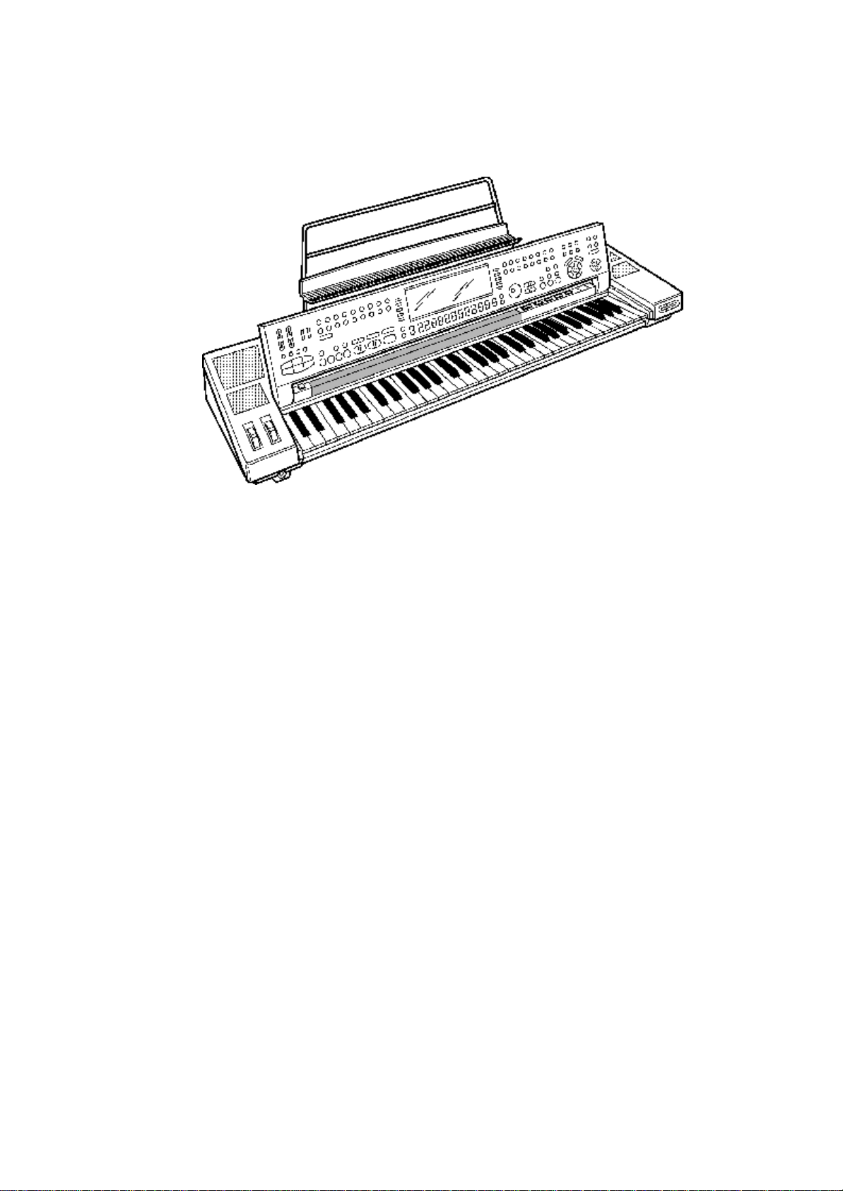
PCM KEYBOARD
SX-KN7000P
SX-KN7000PC
SX-KN7000EX
SX-KN7000EF
SX-KN7000EH
SX-KN7000EQ
SX-KN7000EG
SX-KN7000EB
SX-KN7000EV
SX-KN7000GN
SX-KN7000GM
SX-KN7000GH
SX-KN7000GT
SX-KN7000GU
(P) U.S.A.
(PC) Canada
(EX) Norway, Sweden, Denmark, Finland, Spain, Portugal, Greece,
Poland, Czech,South Africa
(EF) France
(EH) Netherlands
(EQ) Germany
(EG) Austria, Switzerland, Italy
(EB) Great Britain
(EV) Belgium
(GN) Australia, New Zealand
(GM) Malaysia, Singapore
(GH) Hong Kong
1
Page 2
(GT) Taiwan
(GU) Thailand, Indonesia, Dubai, Brazil, Philippines, Barkley(special)
SPECIFICATIONS
SPECIFICATIONS
KEYBOARD
SOUND GENERATOR
MAX. POLYPHONY
61 KEYS (WITH INITIAL
TOUCH)
PCM
128 NOTES
2
Page 3

SOUNDS NUMBER OF SOUNDS:
1236 SOUNDS (1187
SOUNDS + 2 ORGAN
DRAWBARS + 2 ORGAN
TABS + 3 ACCORDION
REGISTERS + 41 DRUM
KITS)
SOUND GROUP:
PIANO, GUITAR,
STRINGS &
VOCAL,BRASS, MALLET
& ORCH PERC, WORLD,
ORGAN &
ACCORDION,SAX &
WOODWIND, PAD ,
SYNTH, BASS, DRUM
KITS, DIGITAL
DRAWBAR, ORGAN
TABS, ACCORDION
REGISTER
SOUND EXPLORER:
Supported
EFFECT PART:
SUSTAIN, DIGITAL
EFFECT, SOUND DSP
GLOBAL:
REVERB, CHORUS,
MULTI, MIC
WHEEL
PITCH BEND,
MODULATION
PART SELECT
RIGHT 1, RIGHT 2, LEFT
TRANSPOSE +/-12 NOTES
RHYTHMS NUMBER OF RHYTHMS:
220 RHYTHMS × 4
VARIATIONS
RHYTHM GROUP:
8 & 16 BEAT, ROCK &
POP, BALLAD, JAZZ &
SWING, MODERN
DANCE, MARCH &
WALTZ, 60s & 70s,SOUL &
R&B, COUNTRY &
WESTERN, ORGANIST,
BALL ROOM, LATIN &
WORLD, ENTERTAINER,
MOVIE & SHOW,
FAVORITES
Supported
3
Page 4

CONTROLS
MAIN VOLUME, APC/
SEQUENCER VOLUME,
LINE IN VOLUME, SD
VOLUME, BALANCE,
MUTE, CONDUCTOR,
START/STOP, INTRO &
ENDING 1, INTRO &
ENDING 2, FILL IN 1, FILL
IN 2, COUNT INTRO,
SYNCHRO&
BREAK,TEMPO/
PROGRAM, TAP TEMPO,
FADEIN/OUT, SPLIT
POINT
PERFORMANCE PADS 20 PRESET BANKS × 6
PADS WITH SOLO
USER BANK × 3,
COMPILE BANKS × 2,
CONTROL PRESET × 1
STOP, AUTO SETTING
AUTO PLAY CHORD
MODE: BASIC,
FINGERED, PIANIST
MEMORY, ON BASS,
CHORD FINDER, LEFT
HOLD
MUSIC STYLE ARRANGER
SOUND ARRANGER
MUSIC STYLIST
ONE TOUCH PLAY
TECHNI-CHORD
PANEL MEMORY
13 BANKS × 8, SET,
Supported
Supported
Supported
Supported
Supported
NEXT BANK, BANK VIEW,
CUSTOM PANEL
SEQUENCER 16 TRACKS
RESOLUTION: 1/96 PER
BEAT
STORAGE CAPACITY:
APPROX.40000 NOTES
(10 SONG MAX.)
INPUT MODES: EASY
RECORD, REALTIME
RECORD, STEP RECORD
FUNCTIONS: RECORD&
EDIT, COPY &
PASTE,RANGE EDIT
4
Page 5

COMPOSER 8 PARTS: BASS,
ACCOMP 1 - 5, DRUMS 1,
2
STORAGE CAPACITY:
APPROX. 13000 NOTES
INPUT MODES: EASY
COMPOSER, REALTIME
RECORD, STEP RECORD
FUNCTIONS: PATTERN
COPY, CUSTOM STYLE
COPY, SEQ TO
COMPOSERCOPY, LOAD
SINGLE COMPOSER
MEMORY: 3 BANKS
DISK DRIVE 3.5 inch DISK DRIVE for
2HD (1.44MB), 2DD
(720KB)
LOAD, SAVE, DIRECT
PLAY, SONG MEDLEY,
DISK TOOLS,
PREFERENCES, STYLE
CONVERT, CUSTOM
STYLE LOAD/SAVE
SD CARD
LOAD, SAVE,
FAVORITES SONGS,
TECHNICS SONG
MEDLEY, SD-AUDIO
PLAY, SD-SOUND PLAY,
CUSTOM STYLE LOAD/
SAVE, SD CARD TOOLS,
SD PREFERENCES
SOUND SETTING
PART SETTING, MIXER,
MASTER TUNING, KEY
SCALING, TECHNI-
CHORD, SOUND LOAD
OPTION, APC REVERB
SETTING, MONITOR
SETTING, SEPARATE
SETTING
SOUND EDIT EASY EDIT, TONE,
PITCH, FILTER,
AMPLITUDE, LFO,
EFFECT, CONTROLLER
MEMORY: 40, 1 USER
DRUM KIT
5
Page 6

REVERB & EFFECT
MIC REVERB & EFFECT,
SOUND LOAD OPTION,
ALLOCATION, MIXER,
SOUND DSP, MULTI,
CHORUS, REVERB,
EQUALIZER
CONTROL
INITIAL, OVERALL
TOUCH SENSITIVITY,
FOOT CONTROLLERS,
PANEL MEMORY MODE,
MUSIC STYLE
ARRANGER MODE, FADE
IN/OUT SETTING
CUSTOMIZE
HOME PAGE SETTING,
FAVORITE SETTING,
DISPLAY TIME OUT,
WALL PAPER SETTING,
MIDI SETTING LOAD
OPTION, DATA
PROTECTION,
LANGUAGE SELECT,
DISK PREFERENCE,
VIDEO OUT MODE
SETTING
MIDI
PART SETTING,
CONTROL MESSAGES,
REALTIME MESSAGES,
COMMON SETTING,
INPUT/OUTPUT SETTING,
MIDI PRESETS, MODE
SETTING, PROGRAM
CHANGE MIDI OUT,
PANEL MEMORY
OUTPUT, COMPUTER
CONNECTION
DISPLAY LCD
PAGE, CONTRAST, EXIT,
DISPLAY HOLD
HELP
DEMO
Supported
Supported
6
Page 7
TERMINALS
OUTPUT
SPEAKERS
POWER REQUIREMENT 75 W
DIMENSIONS (W×H×D)
NET WEIGHT
ACCESSORIES
PHONES, FOOT SW 1, 2,
FOOT CONTROLLER,
EXP PEDAL, MAIN OUT (R
/MONO,L), SUB OUT (1,2)
AUX IN (R/MONO,L), LINE
IN (R/MONO,L), USB,
VIDEO OUT, MIDI (IN/
BASS PEDAL,
OUT,THRU), MIC
66 W (18 W × 2 FOR MID/
HIGH, 30 W × 1 FOR
BASS)
12 cm × 2, 6.5 cm × 2
FOR MID/HIGH, 14 cm × 1
FOR BASS
AC120/220/240V 50/60 Hz
AC120V 60 Hz (NORTH
AMERICA AND MEXICO)
AC230-240V 50/60 Hz
(EUROPE, AUSTRALIA
AND NEW ZEALAND
114 cm × 17 cm × 41 cm
(44-7/8” × 6-11/16” × 16-1/
8”)
17.6 kg (38.8 lbs)
AC CORD, MUSIC
STAND, STYLE CONVERT
DISK, INITIAL DATA
DISK, CD-ROM(AUDIO
RECORDER, SONG
MANAGER, USB DRIVER),
SD CARD
1. Warning
1
7
Page 8

To prevent the risk of fire, smoke, or electrical shock and to ensure safe operation,
please be sure to follow the safety guidelines below.
1. At places where special caution is required, the necessary safety precautions are
clearly labeled or printed, for example, on the cabinet, or on the part concerned.
Please follow these safety precautions, and also those listed in the Owner'sManual.
2. Parts which have a ; mark in the circuit diagram or in the parts list are essential
for safety. When replacing these parts, be sure to use onlythe specified parts.
3. Use the specified types for internal wiring (double-insulated wiring, etc.).
4. When replacing parts on the AC primary side (power transformer, electric switch,
electrical cord, noise-prevention condenser, etc.), wind the lead wire and secure it
by soldering.
5. Do not let the wiring come into contact with heat-emitting devices (fuse resistor,
radiator plate, etc.).
6. When replacing the wiring, make sure that it is not in contact with the unfinished or
rough edge of a part.
7. When replacing the power cord (except for the plug-in type), tug it from various
directions to confirm that it does not slip out of place.
8. Spacing
If soldering was done on the AC primary circuit, confirm that the interval between
the soldered terminals or between the terminal and surrounding metallic parts is at
least the minimum required (between the primary circuit and the chassis: atleast6.5
mm; between primary circuit terminals: at least 4.0 mm; between primary circuit
terminals and secondary circuit terminals: at least 6.5 mm.).
2. Safety Precaution
2.1. Safety Precaution
1. Before servicing, unplug the power cord to prevent an electric shock.
2. When replacing parts, use only the manufacturer’s recommended components for
safety.
3. Check the condition of the power cord. Replace if wear or damage is evident.
4. After servicing, be sure to restore the lead dress, insulation barriers, insulation
papers, shields, etc.
5. Before returning the serviced equipment to the customer, be sure to make the
following insulation resistance test to prevent the customer from being exposed to
a shock hazard.
8
Page 9
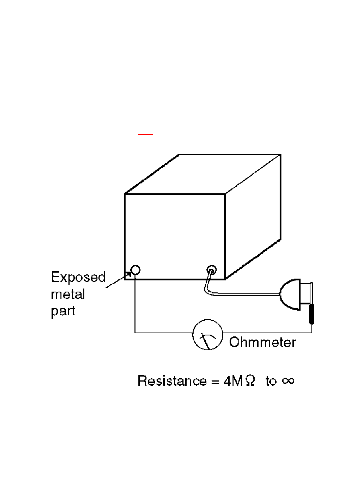
2.2. Insulation Resistance Test
1. Unplug the power cord and short the prongs of the plug with a jumper wire.
2. Turn on the power switch.
3. Measure the resistance value with an ohmmeter between the jumpered AC plug and
each exposed metal cabinet part, such as screw heads, connectors, control shafts,
handle brackets, etc. Measurements should range from 4 MOhm to infinity for
allexposedparts. (refer to Fig.1 )
Fig.1
3. OWNERS MANUAL
9
Page 10
4. MIDI Implementation Chart
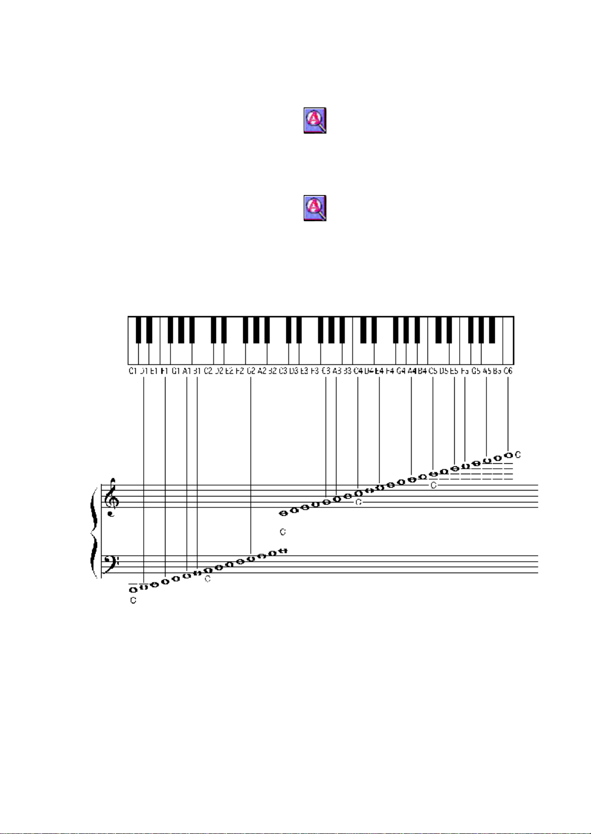
5. Keyboard Ranges
This keyboard features Touch Response, by which you control the volume by playing
the keys harder or softer.
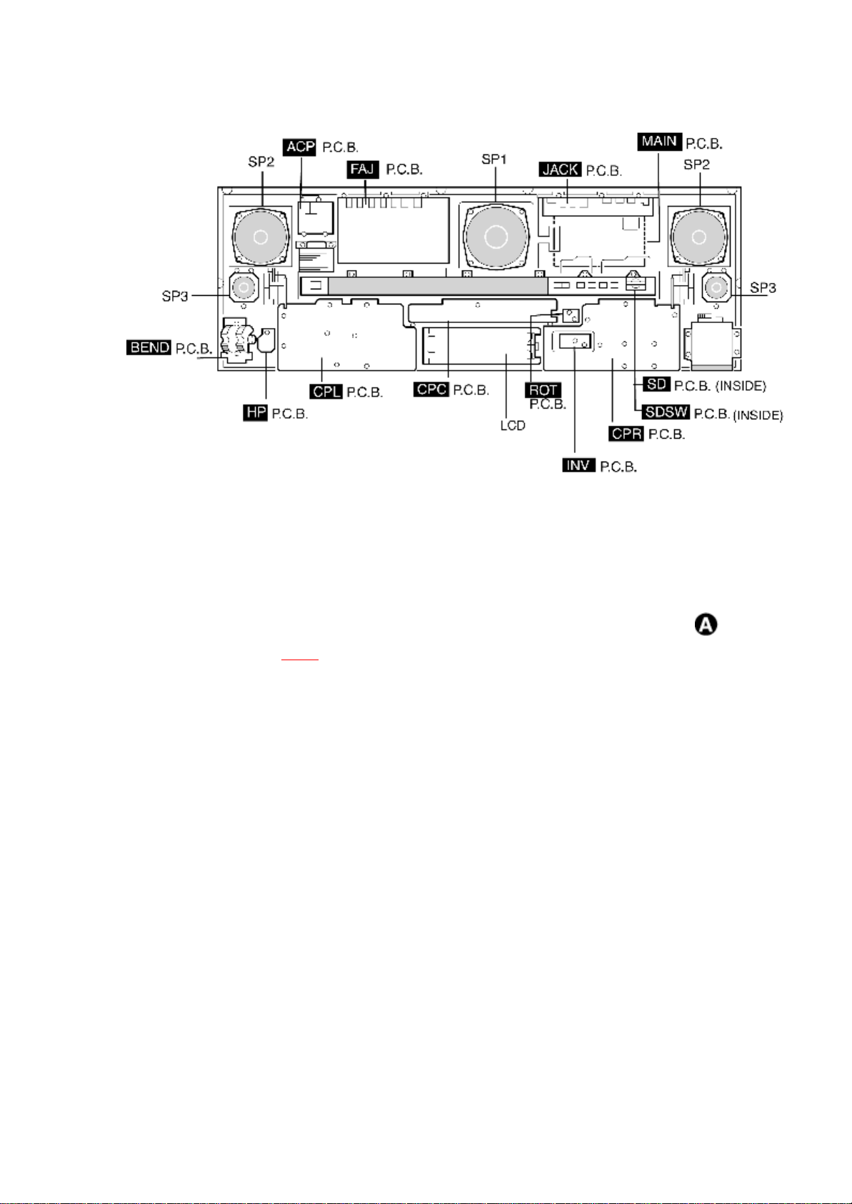
6. Parts Location
10
Page 11
7. Disassembly Instructions
7.1. Removing the top cabinet
1. Turn the keyboard cabinet upside down, and remove the bottom screws ( 17
pcs.) as shown in Fig.2 .
2. Place the keyboard bottomside down, and open the top cabinet .
Fig.2
11
Page 12
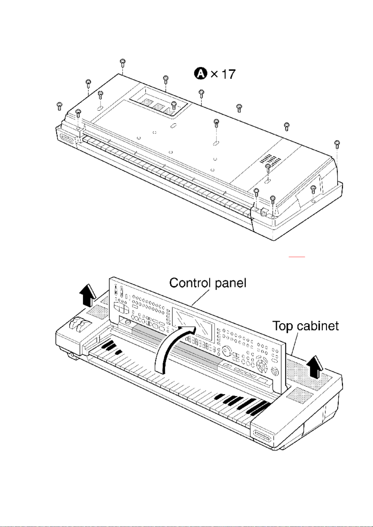
- The control panel is set up, and remove the top cabinet as shown in Fig.3 .
Fig.3
7.2. Removing the control panel, power SW panel, SD panel,
12
Page 13
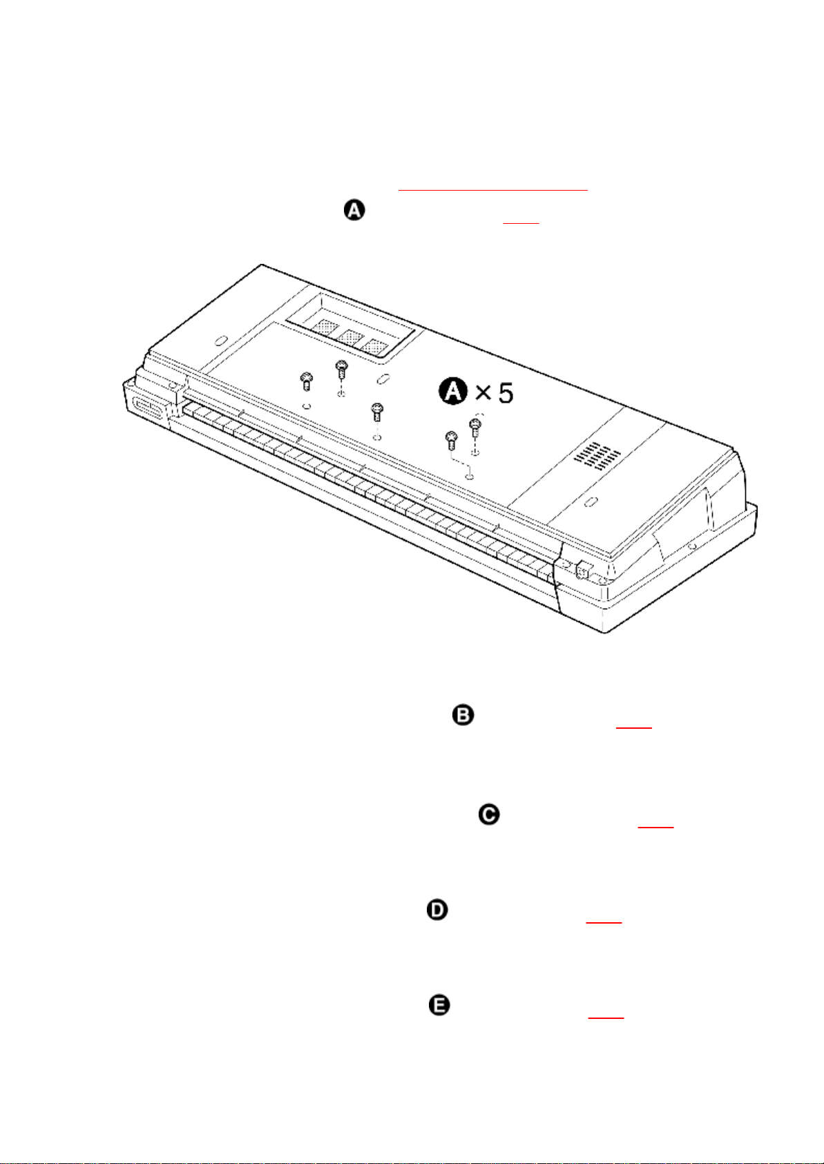
net panel and keyboard unit
- Remove the top cabinet (see step “Removing the top cabinet ”).
- Remove the bottom screws( 5pcs.) as shown in Fig.4
Fig.4
Control panel
1. Place the keyboard bottomside down.
2. Remove the control panel holding screws ( 4pcs.) as shown in Fig.7 .
Power SW panel
- Remove the power SW panel holding screws ( 2pcs.) as shown in Fig.7 .
SD panel
- Remove the SD panel holding screws ( 2pcs.) as shown in Fig.7 .
Net panel
- Remove the net panel holding screws ( 4pcs.) as shown in Fig.7 .
13
Page 14
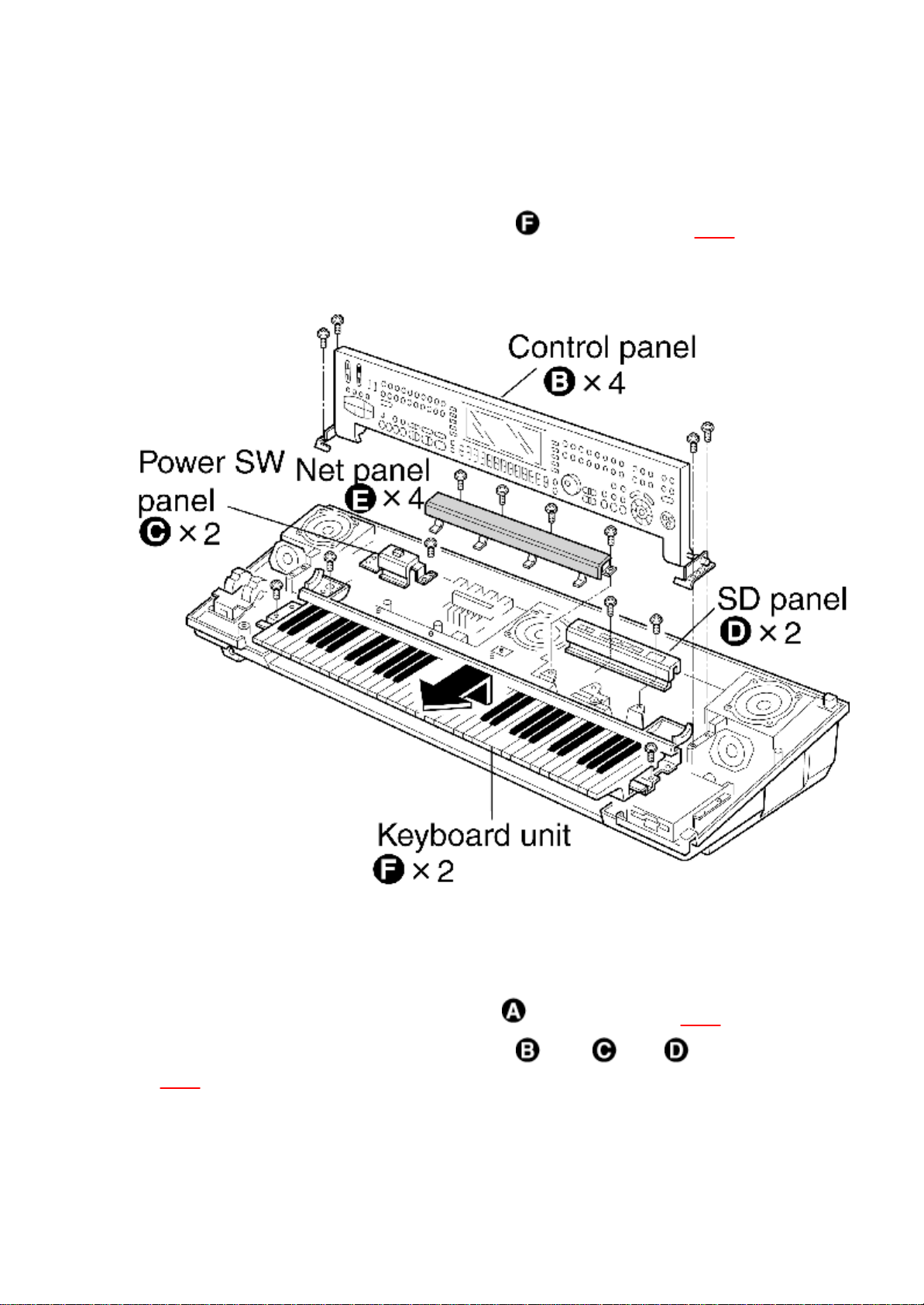
Keyboard unit
- Remove the keyboard unit holding screws ( 2pcs.) as shown in Fig.7 .
Fig.5
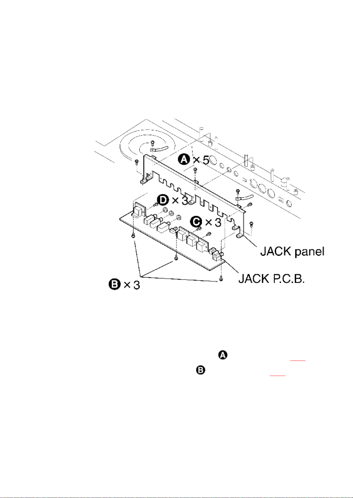
7.3. Removing the JACK and MAIN printed circuit boards
JACK P.C.B.
1. Remove the jack panel mounting screws ( 5pcs.) as shown in Fig.6 .
2. Remove the JACK P.C.B. mounting screws ( 3 pcs., 3pcs, 3pcs.)as shown in
Fig.6 .
Fig.6
14
Page 15
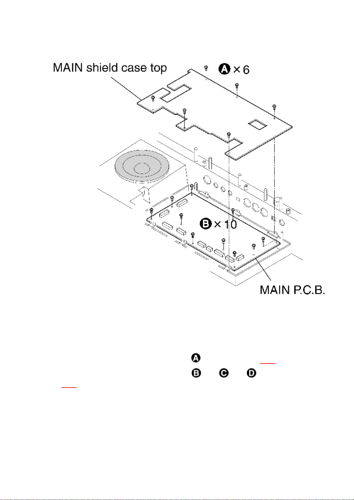
MAIN P.C.B.
1. Remove the main shild top case mounting screws ( 6 pcs.) as shown in Fig.7 .
2. Remove the MAIN P.C.B. mounting screws ( 10pcs.) as shown in Fig.7 .
Fig.7
15
Page 16
7.4. Removing the FAJ printed circuit board
FAJ P.C.B.
1. Remove the FAJ angle mounting screws ( 3pcs.) as shown in Fig.8 .
2. Remove the FAJ P.C.B. mounting screws ( 6pcs., 3pcs, 9pcs.)as shown in
Fig.8 .
Fig.8
16
Page 17
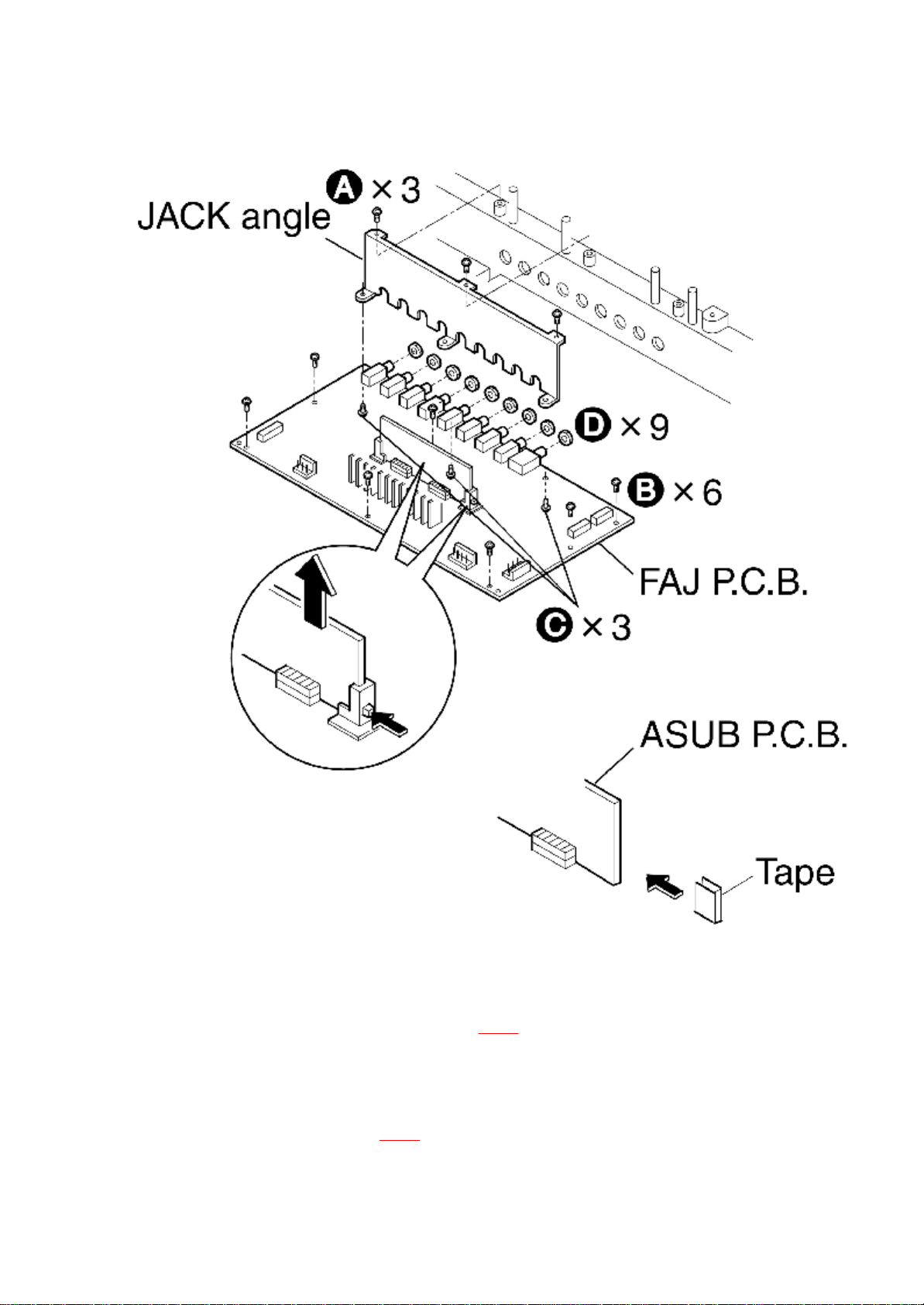
ASUB P.C.B. disasemble
- Push the board holder libs as shown in Fig.8 .
ASUB P.C.B. asemble
- Paste the tape as shown in Fig.8
17
Page 18

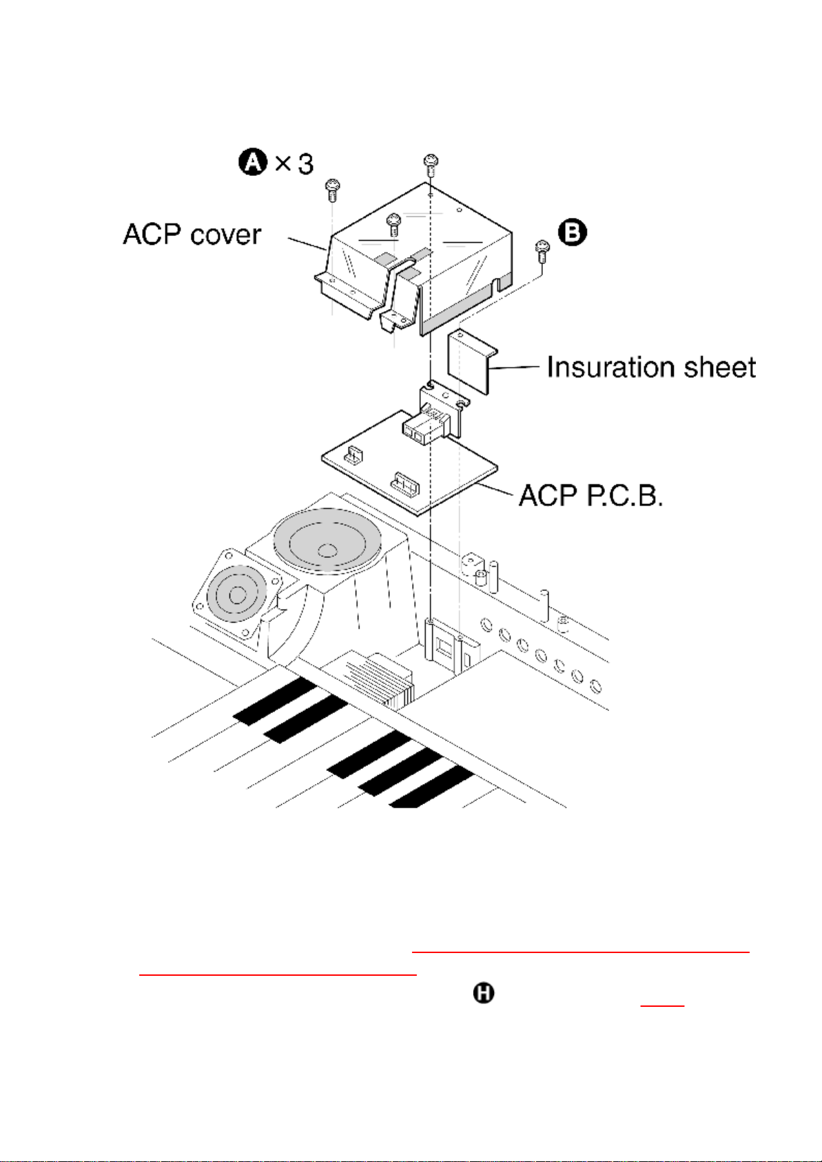
7.5. Removing the ACP printed circuit board
ACP P.C.B.
1. Remove the ACP cover mounting screws ( 3pcs.) as shown in Fig.9 .
2. Remove the ACP P.C.B.and insuration sheet mounting screw ( pc.) as shown in
Fig.9 .
Fig.9
18
Page 19
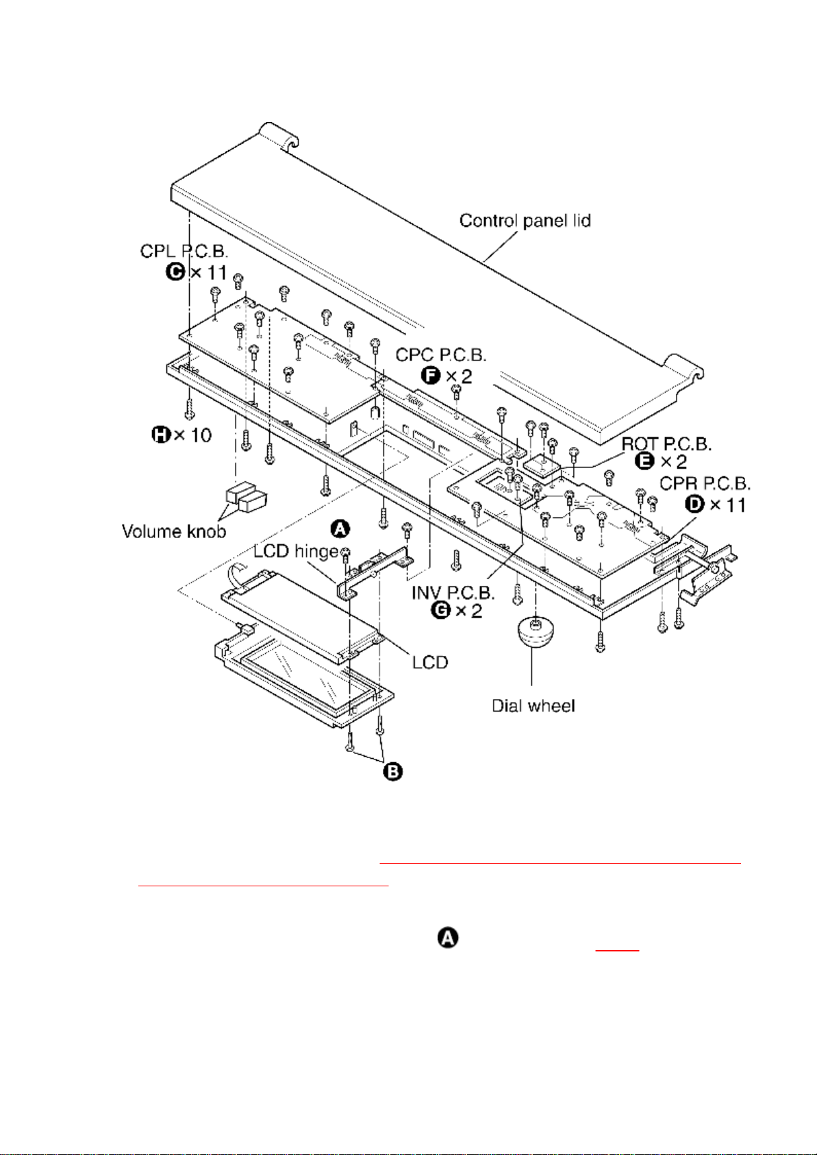
7.6. Removing the LCD, CPL, CPC, CPR, ROT and INV
printed circuit boards
- Remove the control panel (see step “Removing the control panel, power SW panel,
SD panel, net panel and keyboard unit ”).
- Remove the control panel lid holding screws ( 10pcs.)as shown in Fig.10 .
19
Page 20
LCD
1. Remove the LCD hinge holding screws ( 2pcs.) as shown in Fig.10 .
2. Remove the LCD holding screws ( 2pcs.) as shown in Fig.10 .
CPL P.C.B.
1. Pull off the SLIDE VOLUME knob as shown in Fig.10 .
2. Remove the CPL P.C.B. mounting screws ( 11 pcs.) as shown in Fig.10 .
CPR P.C.B.
- Remove the CPR P.C.B. mounting screws ( 11 pcs.) as shown in Fig.10 .
ROT P.C.B. , CPC P.C.B. and INV P.C.B.
1. Pull off the TEMPO/PROGRAM dial as shown in Fig.10 .
2. Remove the ROT P.C.B. mounting screws ( 2 pcs.) as shown in Fig.10 .
3. Remove the CPC P.C.B. mounting screws ( 2pcs.) as shown in Fig.10 .
4. Remove the INV P.C.B. mounting screws ( 2 pcs.) as shown in Fig.10 .
Fig.10
20
Page 21
7.7. Removing the SD and SDSW printed circuit boards
- Remove the SD panel (see step “Removing the control panel, power SW panel, SD
panel, net panel and keyboard unit ”).
SD P.C.B.
- Remove the SD P.C.B. mounting screws ( 2pcs.) as shown in Fig.11 .
SDSW P.C.B.
21
Page 22
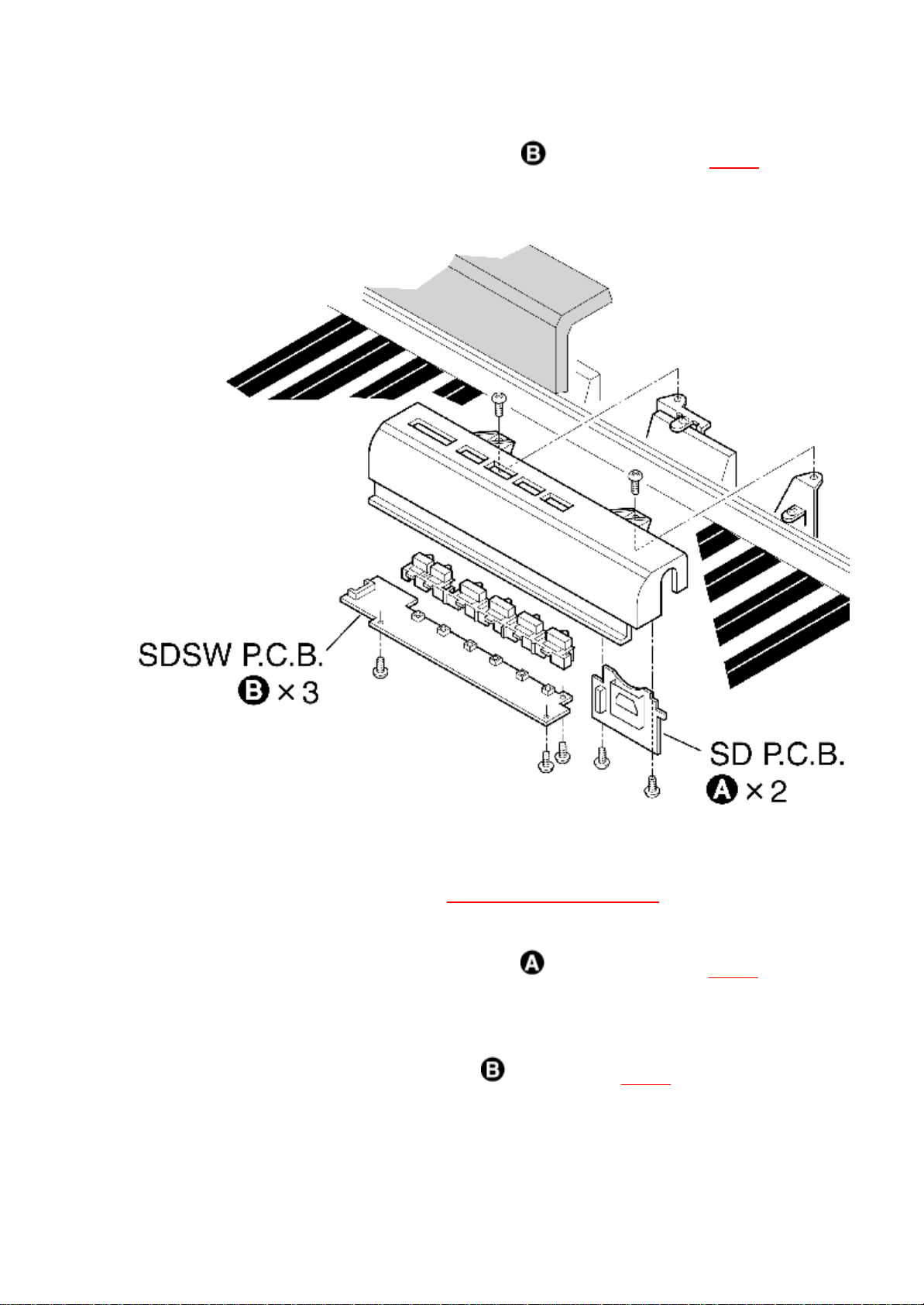
- Remove the SDSW P.C.B. mounting screws ( 3 pcs.) as shown in Fig.11 .
Fig.11
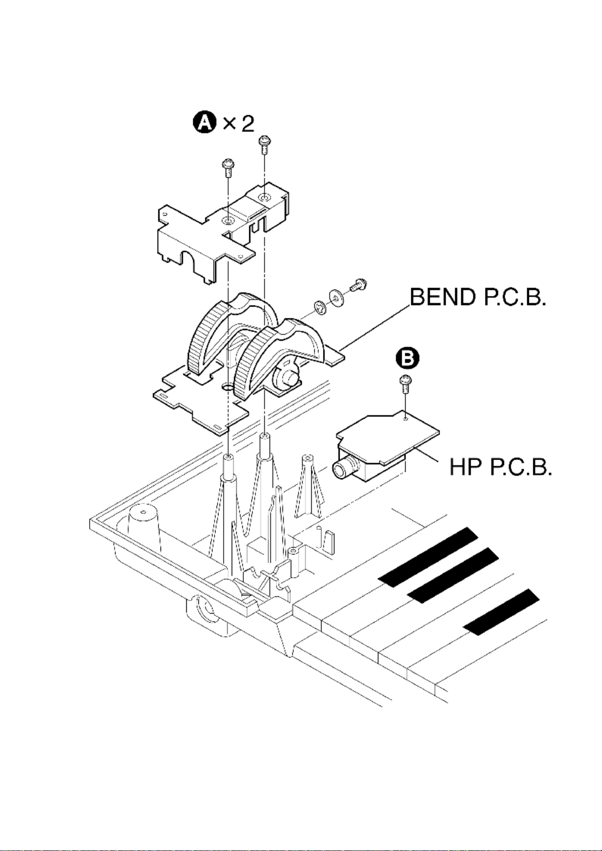
7.8. Removing the BEND and the HP P.C.B.
- Remove the top cabinet (see step “Removing the top cabinet ”).
BEND P.C.B.
- Remove the BEND P.C.B. mounting screws ( 2 pcs.) as shown in Fig.12 .
HP P.C.B.
- Remove the HP P.C.B. mounting screw( ) as shown in Fig.12 .
Fig.12
22
Page 23
7.9. Removing the Disk Drive Unit
23
Page 24
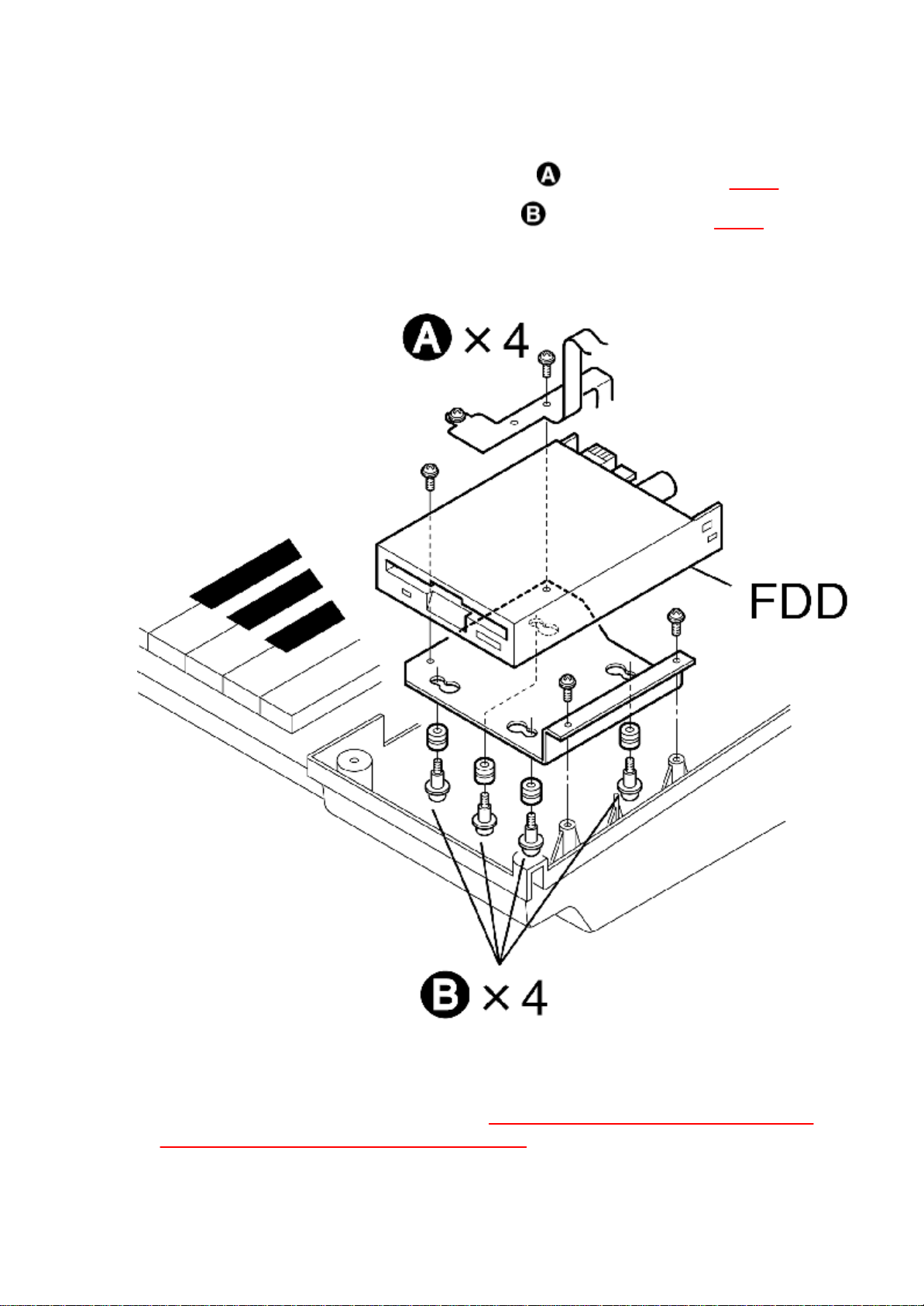
1. Remove the Disk Drive unit mounting screws ( 4 pcs. ) as shown in Fig.13 .
2. Remove the Disk Drive unit holding screws ( 4 pcs. ) as shown in Fig.13 .
Fig.13
7.10. Removing the Power SW
1. Remove the Power SW panel (see step “Removing the control panel, power SW
panel, SD panel, net panel and keyboard unit ”).
24
Page 25
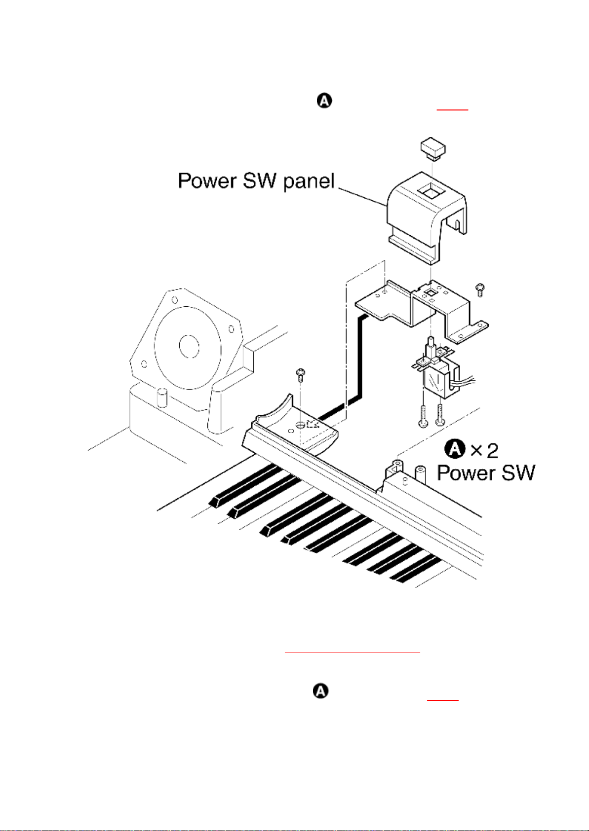
2. Remove the power SW mounting screws ( 2pcs. ) as shown in Fig.14 .
Fig.14
7.11. Removing the 14cm SP, 12cm SP and 6.5cm SP
- Remove the top cabinet (see step “Removing the top cabinet ”).
14 cm SP
- Remove the 14 cm SP@holding screws ( 4pcs.) as shown in Fig.15 .
25
Page 26
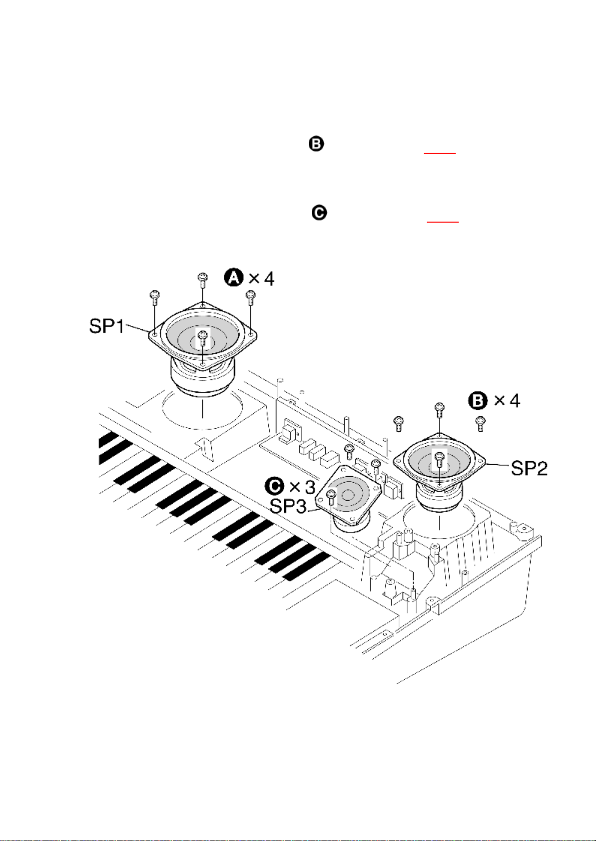
12 cm SP
- Remove the 12 cm SP holding screws ( 4pcs.) as shown in Fig.15 .
6.5 cm SP
- Remove the 6.5 cm SP holding screws ( 4pcs.) as shown in Fig.15 .
Fig.15
7.12. Removing the keys
26
Page 27
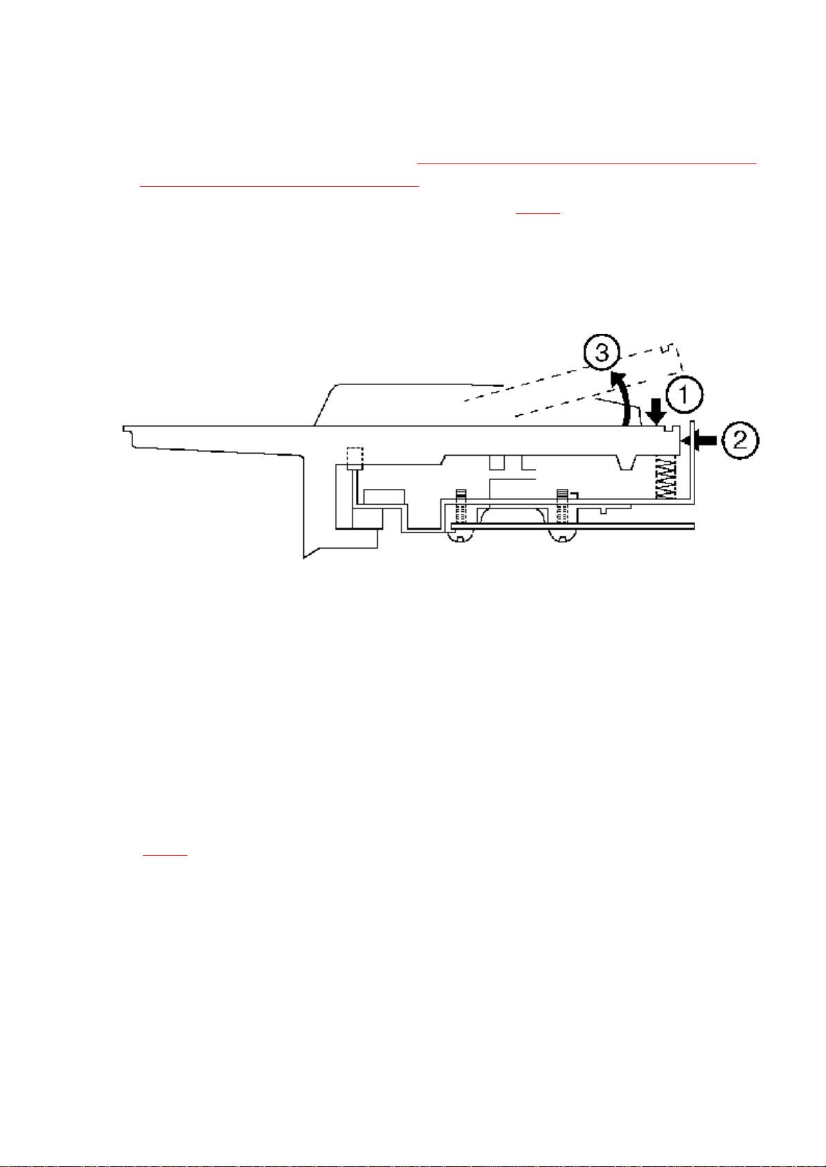
- Remove the keyboard unit (see step “Removing the control panel, power SW panel,
SD panel, net panel and keyboard unit ”).
1. Press downward on the rear of the key as shown in Fig.16 .
2. While pressing downward on the rear of the key, push the key forward and release it
from the chassis.
3. Lift the key and remove it from the chassis.
Fig.16
NOTE:
To remove a black key, the white key to either side of it should be removed first.
8. Service Diagnostic Function
The service diagnostic function makes it possible to determine whether the various
test modes pass or fail. The test modes are completely independent of one another.
Select a test mode as necessary, and run the test.
To set to the service diagnostic mode:
1. Press and hold the C#3, D#3, C#4 keys, and then turn on the power switch. (refer to
Fig.20 )
Fig.20
27
Page 28
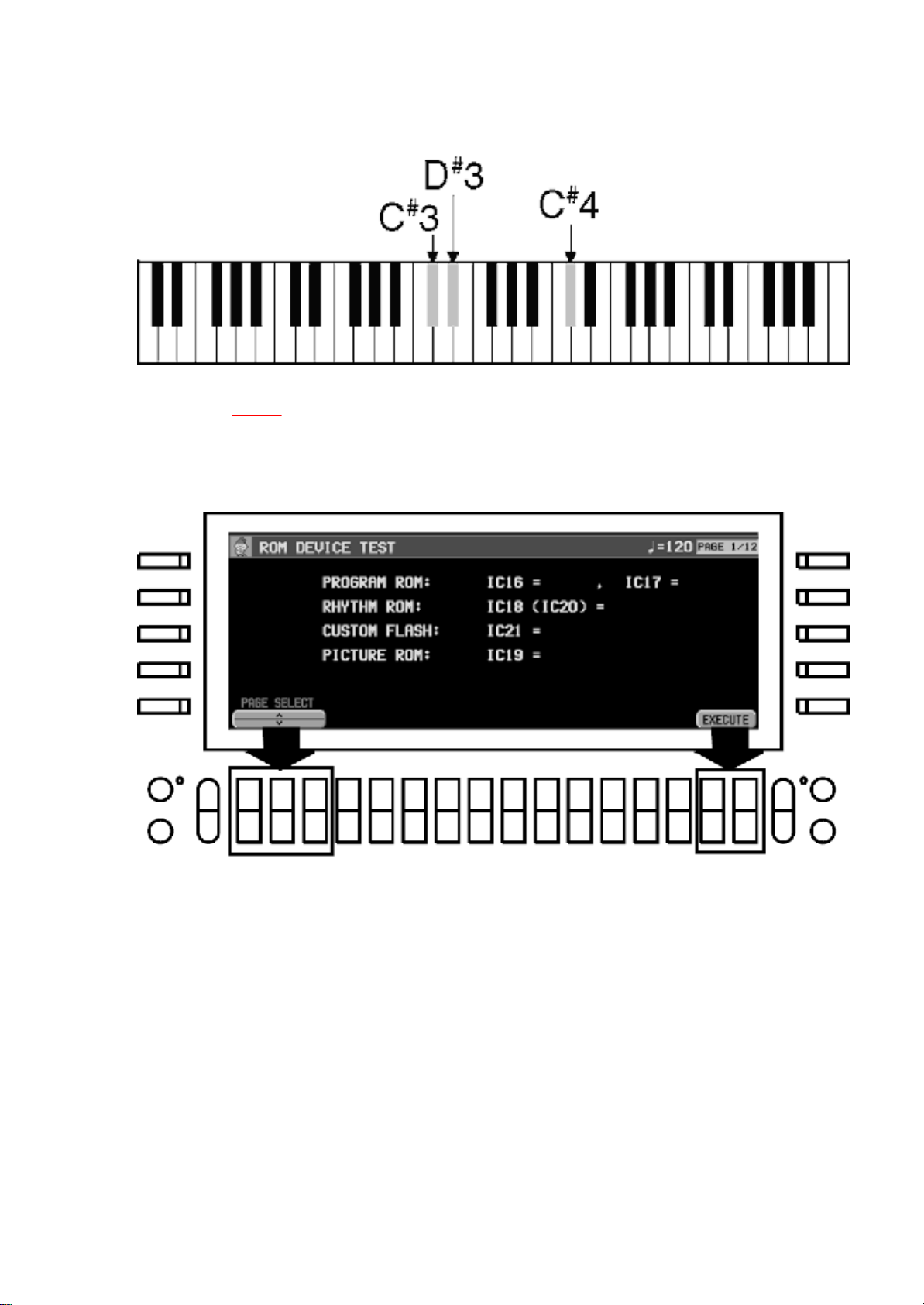
2. After the service diagnostic screen is displayed on the LCD, release the three keys.
(refer to Fig.21 )
3. Use the corresponding buttons below the “page select” display to select the
respective test.
Fig.21
8.1. ROM device test
Fig.22
28
Page 29
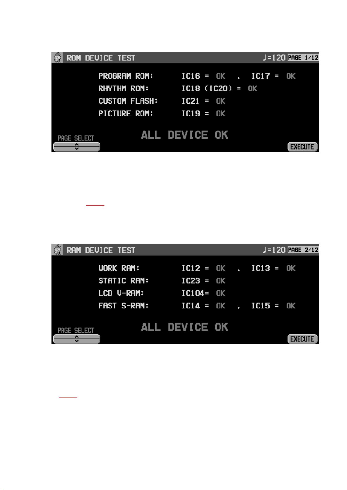
- Press the EXECUTE button to begin the test.
- The test result (OK or NG) is displayed within twenty seconds. If the test result is
NG, not only the respective IC, but also a break or short circuit in the ADDRESS/
DATA BUS as well as in any of the strobe signal lines may be the causeof thefailure.
(refer to Fig.22 )
8.2. RAM device test
Fig.23
- Press the EXECUTE button to begin the test.
- The test result (OK or NG) is displayed within a few seconds. If the test result is NG,
not only the respective IC, but a break or short circuit in the ADDRESS/DATA BUS
as well as in any of the strobe signal lines may be the causeofthe failure. (refer to
Fig.23 )
8.3. Other device test
Fig.24
29
Page 30
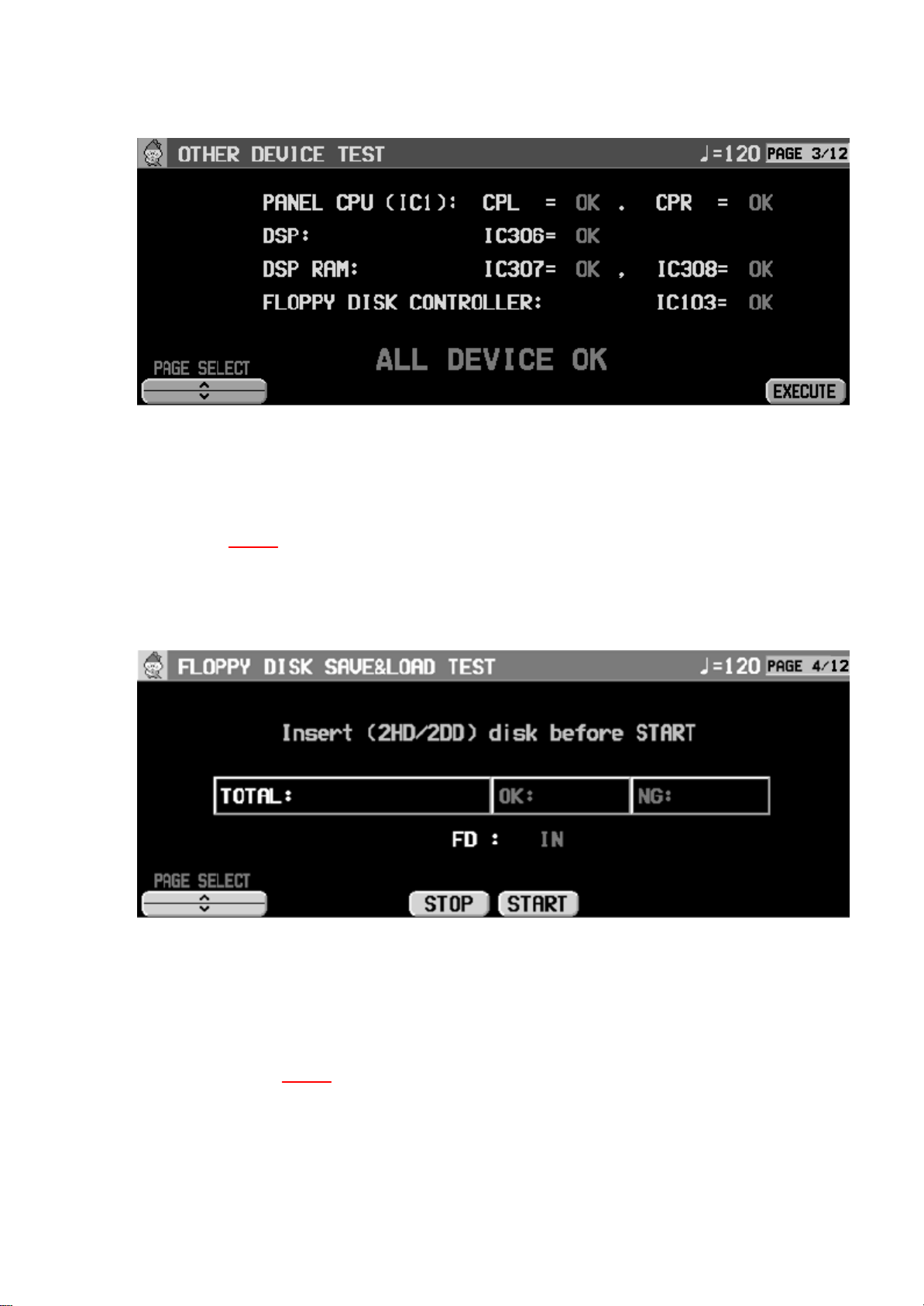
- Press the EXECUTE button to begin the test.
- The test result (OK or NG) is displayed with in a few seconds. If the test result is
NG, not only the respective IC, but also a break or short circuit in the ADDRESS/
DATA BUS as well as in any of the strobe signal lines may be thecause of thefailure.
(refer to Fig.24 )
8.4. Floppy Disk SAVE/LOAD test
Fig.25
- Insert a formatted floppy disk into the Disk Drive. Press the START button to begin
the test.
- The test is carried out repeatedly. Data is saved and loaded, and then the two data
sets are compared. The number of times that the test results in OK or NG are
counted and displayed on the LCD. To interrupt the test, press the STOP
button.(referto Fig.25 )
- Even when the Floppy Disk Drive is functioning properly, the test can result in NG.
If this happens frequently, clean the magnetic heads of the Floppy Disk Drive with a
30
Page 31

cleaning disk. Then, change the disk used in testing with another disk
andreperformthe test. If the trouble is not solved, it is likely that the Disk Drive unit
or some other part of the hardware is broken.
8.5. Panel SW & LED test
Fig.26
- Press all the buttons on the Control Panel and confirm that the corresponding LED
lights.
- If an LED fails to light, the cause may be a defective switch or a break in the
surrounding circuit, etc.
- After all the buttons have been pressed, all the PANEL MEMORY LEDs light. If all
switches are OK, “ALL DEVICE OK” is shown on the LCD. (If a switch is defective,
nothing is shown.) (refer to Fig.26 )
- To light all the LEDs, press and hold the DEMO button. If an LED fails to light, the
LED may be defective or there may be a break in the surrounding circuit.
8.6. LCD module test (LCD adjustment and confirmation)
Fig.27
31
Page 32

- Press the RGBWB, CROSSTALK, SAMPLE, CONTRAST or VIDEO OUT button to
begin the respective test. (refer to Fig.27 )
RGBWB:
All the dots light in red, green, blue, white, and finally black. The display can be held
by pressing the DISPLAY HOLD button.
CROSSTALK:
An H pattern is shown. LCD crosstalk can be evaluated. To exit this test, press the
EXIT button.
SAMPLE:
Several display patterns shown during normal use are shown. The display can be
held by pressing the DISPLAY HOLD button.
CONTRAST:
The test pattern is shown. Adjust the contrast by the CONTRAST control on the
right of the LCD. To exit this test, press the EXIT button.
VIDEO OUT :
Check each display mode of PAL and NTSC. To exit this test, press the EXIT button.
- If the correct display is not shown during these tests, the LCD or LCD drive circuit
may be defective.
8.7. In & Out interface test
Fig.28
32
Page 33

- The operation status of each input action part can be confirmed. If the part is
operating properly, “OK” is shown, excluding the Expression Pedal. (refer to Fig.28
)
- When a keyboard key is pressed, the corresponding pitch and velocity aftertouch is
displayed (only as long as the key is depressed).
- The respective statuses for other input action parts are displayed. (Analog parts are
shown as numerical values from 0 to 255, and switches are shown as ON or OFF.)
- If the display fails to change when the part is operated, or if the change is abnormal,
it may indicate a defective part.
8.8. MIDI IN/OUT test
Fig.29
- First, set the COMPUTER terminal switch to MIDI.
- Use a MIDI cable to directly connect the MIDI IN and MIDI OUT terminals.
- When a keyboard key is pressed, the transmitted and received data are compared
33
Page 34

and the MIDI terminal operation is indicated as being OK or NG. (refer to Fig.29 )
- If NG is shown, check both the IN and OUT terminals, as well as the circuit.
8.9. WAVE ROM test
Fig.30
- Press the EXECUTE button to start the test.
- The test result (OK or NG) is displayed within thirty seconds. If the test result is NG,
not only the respective IC, but also a break or short circuit in the ADDRESS/DATA
BUS as well as in any of the strobe signal lines may be the causeofthe failure. (refer
to Fig.30 )
8.10. SOUND SYSTEM test
Fig.31
- Use the button in the SOUND GROUP to select an item from 1 to 6 (refer to Fig.31
and Fig.32 ). Press a keyboard key.
34
Page 35

Fig.32
1. Generate a full amplitude sine wave in the pitch of each key. (No touch, fixed stereo
center).
If no sound is generated or if the sound is distorted, the sound generator ROM
corresponding to the key position is defective.
2. For confirming the output pathway from the sound generator. (Fixed scale, no touch)
The Lch and Rch sound outputs are confirmed separately.
3. Generate a full amplitude sine wave in the pitch of each key +2 octaves. (No touch,
fixed stereo center)
By generating a sound frequency outside the normal keyboard zone, you can
confirm whether or not there is an abnormality in the sound output frequency zone.
4. Generates a full amplitude sine wave in the pitch of each key -2 octaves. (No touch,
fixed stereo center)
By generating a sound frequency outside the normal keyboard zone, you can
confirm whether or not there is an abnormality in the sound output frequency zone.
5. Generate a sine wave in the pitch of each key with touch.
You can confirm if the volume changes depending on the touch.
6. Generate a full amplitude sine wave in the pitch of each key at a -16 dB volume. (No
touch, fixed stereo center)
You can confirm the same sound output as in 1, at a lower volume.
8.11. SD test
Fig.33
35
Page 36

Load/save test
- Insert the SD card. Press the START button to begin the test.
- The test is carried out repeatedly. Data is saved and loaded, and then the two data
sets are compared. The number of times that the test results in OK or NG are
counted and displayed on the LCD. To interrupt the test, press the STOP
button.(referto Fig.25 )
Audio test
- Insert the SD card. Press the START button to begin the test.
8.12. WAVE EXPANSION BOARD test
Fig.34
- Insert the SY-EW01,EW02,,EW03 or EW04 board.
36
Page 37

- Press the EXECUTE button to start the test.
- The test result (OK or NG) is displayed . If the test result is NG, not only the
respective IC, but also a break or short circuit in the ADDRESS/DATA BUS as well
as in any of the strobe signal lines may be the causeof the failure. (referto Fig.30 )
9. Precautions before Servicing the Main Circuit
This model employs a FLASH ROM (EEPROM) for the PROGRAM ROMs and the
CUSTOM DATA ROM. If changing any of these ICs, service the MAIN CIRCUIT as
explained here following.
9.1. About the FLASH ROM
The FLASH ROM can be electrically erased and rewritten. This model is designed so
that the repair technician can easily write and change programs and data in the FLASH
ROM, by using a floppy disk. (refer to Fig.33 )
Fig.33
37
Page 38

9.2. Notes on replacing FLASH ROMs
The replacement parts include a FLASH ROM with a available memory and the
PROGRAM DISKs which contains the program to be written into the PROGRAM
ROMs. After replacing the PROGRAM ROM, always write the program into it from the
38
Page 39

PROGRAM DISKs includedinthe replacement parts. For details on programming, see
“After replacing the PROGRAM ROM (IC16/IC17) ” .
The CUSTOM DATA ROM stores RHYTHM & ACCOMP data for the RHYTHM GROUP/
CUSTOM function. The initial RHYTHM & ACCOMP data is factory-set in the CUSTOM
DATA ROM at the time of shipping. The CUSTOM DATA ROM can also store
COMPOSERdatathat the user creates. However, user-data is lost when the CUSTOM
DATA ROM is replaced. After replacing the CUSTOM DATA ROM, default the data in it
with the INITIAL DATA DISK attached to this product. For details on defaulting, see
“After replacing the CUSTOM DATA ROM (IC18) ”.
9.3. About the replacement parts
The same FLASH ROM with a available memory can be used for the PROGRAM ROMs
(IC16/IC17). Moreover, the included PROGRAM DISKs contains all programs.
Therefore, the replacement parts can be used for IC16 and IC17.
9.4. How to write program/data into FLASH ROMs
9.4.1. After replacing the PROGRAM ROM (IC16/IC17)
1. Set the PROGRAM DISK 1 included in the replacement parts into the Floppy Disk
Drive.
2. Hold down the PANEL MEMORY buttons 1 , 2 , 3 and 4. And turn on the power
switch. (refer to Fig.34 )
Fig.34
39
Page 40

3. Check “Flash Memory Update” is displayed on the LCD, and release the PANEL
MEMORY buttons.
The program will be written into the FLASH ROM automatically. Replace the floppy
disk when instructed.
4. When the operation is complete, “Completed!!” will be displayed on the LCD.
5. Turn the power switch off and then turn it on again. Check the instrument is
functioning properly.
9.4.2. After replacing the CUSTOM DATA ROM (IC18)
1. With the normal display displayed on the LCD, set the INITIAL DATA DISK included
with the model into the Floppy Disk Drive.
The normal display automatically changes to the DISK MENU display.
2. Select “LOAD” to change to the file select display.
3. Move the highlighting cursor to “CTMINI” in “No. 01” and select “LOAD”.
“PLEASE WAIT...” will appear on the LCD and the model will start defaulting data in
the CUSTOM DATA ROM.
40
Page 41

4. When the operation is complete, “Completed!!” will be displayed on the LCD.
METER
READING
5. Turn the power switch off and then back on again. Check the instrument is
functioning properly.
10. Measurements and Adjustments
ADJUSTMENT
TOUCH SENSOR
MEASURING
CONDITIONS
any position Oscilloscope MKB3 P.C.B. VR1 CN11-3pin 5.0V
1. Press one of the any keys hardly and check the CN11-3 pin voltage.
The voltage will increase and become steady.
2. Adjust the voltage to 5.0V with VR1 at that time.
EQUIPMENT
ADJUSTMENT
P.C.B.
ADJ. POINT CONNECT
METER TO
11. Precautions before Servicing
11.1. Precautions for measuring of the output waveforms
1. The waveform was measured with a “National Digital Storage Oscilloscope VP5730A”. Therefore the waveforms of musical tone signals shown may differ
somewhat due to the difference in the timing of triggering.
2. Since the 1/10 test probe is used, the indicated voltage value on the bottom part of
each waveform illustration is 1/10 of the actual value (e.g. 0.2 V/cm should be 2.0 V/
cm).
3. To measure the waveforms, first set this unit to the service diagnostic mode (refer
to “WAVE ROM test ”). The WAVE ROM output will then be output as a sine wave to
facilitate the servicingcheck.
11.2. Important safety notice
- Components identified by a mark have special characteristics impotant for safety.
- When replacing any of these components, use only manufacture’s specified parts.
11.3. Symbolic Marks
The symbolic marks for resistors and capacitors which used in this circuits are
classified as following Table-1 and Table-2 .
11.3.1. RESISTORS
41
Page 42

- Resistors without symbolic mark are FIXED CARBON FILM RESISTORS (ERD-type).
- All resistors are 1/4 WATT, ±5 % TOLERANCE unless otherwise designated in
schematic diagrams.
Table-1
SYMBOL
Fixed Carbon Film Resistors
“FLAME-PROOF” (ERD—F—type)
Fixed Wire Wound Resistors
“FLAME-PROOF” (ERF—type)
Fixed Metal Oxide Film Resistors
“FLAME-PROOF” (ERG—type)
Fixed Metal Film Resistors
“FLAME-PROOF” (ERX—type)
Fixed Metal Film Resistors (Precision and
High Stability)
(ERO—type)
Fuse Type Fixed Metal Oxide Film
Resistors
“FLAME-PROOF” (ERQ—type)
Fuse Type Fixed Carbon Film Resistors
“FLAME-PROOF” (ERD2FC—type)
SPECIFICATION
11.3.2. CAPACITORS
- Capacitors without symbolic mark are POLYESTER CAPACITORS. (ECQM-type,
ECQG-type, ±10% Tolerance)
- Polarized capacitors without symbolic mark are Aluminum Electrolytic Capapcitors.
(ECEA-type, ±20% Tolerance)
Table-2
42
Page 43

SYMBOL
SPECIFICATION TYPE
Non-Polarized Electrolytic
Capacitors
ECEA_KN_type
Non-Polarized Electrolytic (for
Network system)
Tantalum Solid Electrolytic
Capacitors
Metalized Plastic Film
Capacitors (TF Series)
Temperature Compensating
Ceramic Capacitors
High-Dielecytric Constant
Ceramic Capacitors
Axial Lead Ceramic
Capacitors
Metalized Polyester Film
Capacitors for Across the Line
Aluminum Electrolytic
Capacitors for Smoothing
Circuit
Multilayer Ceramic Chip
Capacitors
ECEA_Y_type
ECS_type
ECQV_type
ECC_type
ECK_type
ECR_type
ECB_type
ECQ_EW_type
ECES_type
ECUV_type
12. MEASURING CONDITION
43
Page 44

44
Page 45

13. SCHEMATIC DIAGRAM
45
Page 46

14. Printed Circuit Board
15. Block Diagram
16. Wiring Connection Diagram
17. Replacement Parts List
Notes:
*Important safety notice:
Components identified by mark have special characteristics important for safety.
Funrthermore, special parts which have purposes of fire-retardant (resistors), highquality sound (capacitors),low -noise(resistors), etc. are used.
When replacing any of components, be sure to use only manufacture’s specified parts
shown in the parts list.
*Warning: This product uses a laser diode. Refer to caution statements.
*ACHTUNG:Die lasereinheit nicht zerlegen.Die lasereinheit darf nur gegen einc vom
hersteller spezifizierte einheit ausgetauscht werden.
*Capacity values are in microfarads (uF) unless specified otherwise, P=Pico-farads
(pF) F=Farads (F)
46
Page 47

*Resistance values are in ohms, unless specified otherwise, 1K=1,000 (OHM), 1M=
1,000K (OHM)
*The marking <RTL> indicates that the Retention Time is limited for this item. After the
discontinuation of this assembly in production, it will no longer be available.
*Since SW consists of buttons and P.C.B.’s, we do not supply it as an individual part
(refer to “Manual Keyboard Parts and Control Panel Parts Location ”.).
*[SPC] in Remarks columns parts that are supplied by SPC..
*“<IA>”-“<IG>”, marks in Remarks indicate languages of instruction manuals. [<IA> :
English, <IB> : French, <IC> : Germany, <ID> :Spanish, <IE> : Danish, <IF> :
Netherlands, <IG> : Italian, ]
Ref. No. Part No. Part Name & Description
1 QAQG102AA TOP CASE UNIT 1 P
1 QAQG102AB TOP CASE UNIT 1 EXCEP P
2 QMGG071AA TOP CASE CUSHION 7
3 QYKG326BA NET PANEL ASSY 1
4 XTW3+10Q SCREW 79
5 QYAG3009AB ASSEMBLED MUSIC RACK 1
6 RFKJXKN7000E BOTTOM CASE ASS'Y 1
6 RFKJXKN7000P BOTTOM CASE ASS'Y 1
7 SHGG3130A FOOT 4
8 QLZG022A CORE 3
9 QLZG017A CORE B 7
10 XTW3+14Q SCREW 4
11 K2AA2G000003 AC IN COVER 1 EXCEPT P PC
11 K2AB2G000003 AC IN COVER 1 P PC
12 XYN4+F20 SCREW 4 P PC
12 XYN4+F25 SCREW 4 EXCEPT P PC
13 XTW3+16JFZ SCREW 21
14 QMAG0292AA MAIN LID 1
15 QMRG2061AAK INSULATION SHEET 1 EXCEPT GM GU GT
15 QMRG2063AAK INSULATION SHEET 1 GM GU GT
16 QMRG2120AA ACP COVER 1
17 QQLG241AA CAUTION LABEL 1 P PC
17 QQLG251AA CAUTION LABEL 1 EB
18 QQLG253AA FAJ JACK LABEL 1
19 QQLG254AA MAIN JACK LABEL 1
20 XTV3+10G-M SCREW 14
21 XYE3+FJ10 SCREW 30
22 QLZG025A CORE 1
23 QLZG026A CORE 1
24 QMRG5300AA BBD SHEET 7
25 QSCG138A SHIELD SHEET 1
26 XTW3+10TFZ SCREW 22
27 XTV3+12G SCREW 2
28 SBCG110B POWER BUTTON 1
29 QGPG0166AA P.SW PANEL 1
30 QMRG2123AA P.SW COVER 1
31 QGPG0163AA CONTROL PANEL 1 P
31 QGPG0163AB CONTROL PANEL 1 EXCEPT P
32 QGUG1440AD1K BUTTON 1
Pcs
Remarks
47
Page 48

Ref. No. Part No. Part Name & Description
33 QGUG1536BA BUTTON A -1 2
34 QGUG1536CA BUTTON A -2 1
35 QGUG1536EA BUTTON A -4 1
36 QGUG1536FA BUTTON A -5 1
37 QGUG1537CA BUTTON B 1
38 QGUG1538BA BUTTON C-1 2
39 QGUG1538CA BUTTON C-2 1
40 QGUG1539AA BUTTON D 8
41 QGUG1540BA BUTTON E 3
42 QGUG1541AA BUTTON F 2
43 QGUG1542AA BUTTON G 2
44 QGUG1543BA BUTTON H 2
45 QGUG1544AA BUTTON I 2
46 QGUG1547BA BUTTON L 1
47 QGUG1548AA BUTTON M 1
48 QGUG3002BC DIAL WHEEL 1
49 QGUG1536DA BUTTON A -3 1
50 QGUG1537DA BUTTON B-1 1
51 QGUG1538AA BUTTON C 2
52 QGUG1538CB BUTTON C-3 1
53 QMRG7146AA BUTTON ORNAMENT O 1
54 QGUG1549BA BUTTON N 1
55 QMRG7147AA BUTTON ORNAMENT Q 1
56 QGUG1550AA BUTTON P 1
57 QSLG025AA LCD 1 L5DCDPH00001
58 QMFG1294AA HINGE FELT 2
59 QKWG046AA LCD WINDOW 1
60 QGUG1551AA BUTTON R 1
61 QGUG1552BA BUTTON S 1
62 QHDG052AB SCREW 4
63 QMGG072AA CUSHION 8
64 QMGG072AB CUSHION 2
65 QMRG2121AA WIRING COVER A 1
66 QMRG2122AA WIRING COVER B 1
67 QMRG2127BA DIFFUSSION SHEET 1
68 QMRG5297AA URETHANE FOAM 1
69 QMRG7145AA LCD COVER 1
70 QMRG7148AA BUTTON LIGHTING CHIP 1
71 QMRG7149AA LIGHTING ON/OFF LEVER 1
72 XTB23+10JFZ SCREW 2
73 XTV3+10G-M SCREW 2
74 XTV3+14G SCREW 10
75 QMEG013AA EARTH SPRING A 1
76 QMEG014AA EARTH SPRING B 1
77 QMRG2128AA PROTECT SHEET 1
78 QMRG5298AA BUTTON CUSHION A 1
79 QMRG5299AA BUTTON CUSHION B 2
80 SBNG7070C SLIDE VOL KNOB 2
81 QGKG0183AA FRONT ORNAMENT 1 P
81 QGKG0183AB FRONT ORNAMENT 1 EXCEPT P
82 XTV3+6J MIDI JACK SCREW 5
83 XYE3+FJ10 SCREW 1
84 SBNG4050B BENDER WHEEL 2
85 SHGG5010A TUBE 2
Pcs
Remarks
48
Page 49

Ref. No. Part No. Part Name & Description
86 QMFG4076AAK CUSHION 2
87 QHQG009AA NUT 2
88 SUSG570A SPRING 1
89 XYE3+FJ10 SCREW 3
90 XNS12FZ NUT 9
91 QMEG011AA THERMISTOR SPRING 1
92 QWZG010AA THERMISTOR TUBE 1 FAJ
93 XTV3+10C SCREW 1
94 XYE3+FJ10 SCREW 3
95 XNS12FZ NUT 3
96 XTW3+10TFZ MIDI JACK SCREW 6
97 XTB3+10GFZ VIDEO OUT(1) 1
98 QMFG4107AA CUSHION 1
99 QMGG029AA FLOATING RUBBER 4
100 QAUG033AA FDD UNIT 1
101 QMFG4207AA CUSHION 1
102 QHDG043AA SCREW 4
103 XYN3+F8 SCREW 1
104 XTT4+20CFZ SCREW 32
105 RFKNSXKN7000 SP BOX LID ASS'Y 1
106 QKUG1052AAZ SP BOX LID (B) 2
107 QMRG5277AA SP LID CUSSION (A) 8
108 QMRG5278AA SP LID CUSSION (B) 4
109 QMRG5279AA SP LID CUSSION (C) 2
110 QMRG5280AA SP LID CUSSION (D) 1
111 QMRG5284AA SP LID CUSSION (H) 2
112 QMRG5285AA SP LID CUSSION (I) 2
113 QMRG7141AA BASS PORT COVER 1
114 QGPG0164AA SD PANEL 1
115 QGKG0184BA SD CARD LID 1
116 QGUG1553AA BUTTON V 1
117 QMRG5276BA SD LID CUSSION 2
118 QMRG7144AA EDGE PANEL 1
119 QMBG033AA SD LID SPRING 1
120 QHDG064AA SCREW 5
121 QHDG065AA SCREW 1
122 QWZG011AA LED TUBE 1
123 QGPG0167BA CP LID 1 P
123 QGPG0167BB CP LID 1 EXCEPT P
130 QMRG5297AA URETANE FORM 1
131 QMRG5301AA ORNAMENT CAP 1
132 QMRG5302AA ACOUSTIC MATERIAL 1
133 QMRG5303AA CORE HOLDING TAPE 1
134 QMRG5304AA CORE HOLDING SHEET 1
135 QMRG5305AA URETAN SHEET 1
136 QMRG5306AA PEF SHEET 1
137 QMRG5307AA URETANE FORM 4 GU GM GT
138 QQLG167AA VOLT ADJ LABEL 1
139 QKCG003 CP HING (R) 1
140 QKCG004 CP HING (L) 1
141 QKCG005 LCD HING 1
142 QMRG5243AB URETANE FORM 4
143 QMRG5247AB URETANE FORM 1
144 QEXGRA01010U CONNECTION WITH WIRE 1
Pcs
Remarks
49
Page 50

Ref. No. Part No. Part Name & Description
201 XYE3+FJ10 SCREW 2
202 QMWG6009BAK 13KEYS RUBBER SWITCH 1
203 QMWG6010BA 12KEYS RUBBER SWITCH 4
204 QMFG4176AAK CUSHION 1
205 QMRG2074AAK HOLDING SHEET 1
206 QMWG5003CA AFTER TOUCH SENSOR 1
207 XTW3+10T SCREW 37
208 SHGG9052A KEY GUIDE RUBBER 61
209 QMFG1120CA FELT 1
210 STBG1101B WHITE KEY(C F) 10
211 STBG1111B WHITE KEY(D) 5
212 STBG1121B WHITE KEY(E B) 10
213 STBG1131B WHITE KEY(G) 5
214 STBG1141B WHITE KEY(A) 5
215 STBG1151B WHITE KEY(CC) 1
216 STBG2071AK BLACK KEY 25
A1 QQFGKN7000AA FAN BAG 1 P
A1 QQFGKN7000BA FAN BAG 1 PC
A1 QQFGKN7000CA FAN BAG 1 EX
A1 QQFGKN7000DA FAN BAG 1 EQ
A1 QQFGKN7000EA FAN BAG 1 EB
A1 QQFGKN7000FA FAN BAG 1 EG
A1 QQFGKN7000GA FAN BAG 1 EF
A1 QQFGKN7000HA FAN BAG 1 EH
A1 QQFGKN7000JA FAN BAG 1 EV
A1 QQFGKN7000KA FAN BAG 1 GU GM GH GT
A1 QQFGKN7000LA FAN BAG 1 GN
A1-1 QQTG0671A INSTRUCTION MANUAL 1 P <IA>
A1-1 QQTG0671A INSTRUCTION MANUAL 1 PC<IA>
A1-1 QQTG0671A INSTRUCTION MANUAL 1 EX<IA>
A1-1 QQTG0671A INSTRUCTION MANUAL 1 GN<IA>
A1-1 QQTG0671A INSTRUCTION MANUAL 1 GM<IA>
A1-1 QQTG0671A INSTRUCTION MANUAL 1 GH<IA>
A1-1 QQTG0671A INSTRUCTION MANUAL 1 GU<IA>
A1-1 QQTG0671A INSTRUCTION MANUAL 1 GT<IA>
A1-1 QQTG0671A INSTRUCTION MANUAL 1 EB<IA>
A1-1 QQTG0672A INSTRUCTION MANUAL 1 PC<IB>
A1-1 QQTG0672A INSTRUCTION MANUAL 1 EG<IB>
A1-1 QQTG0672A INSTRUCTION MANUAL 1 EV<IB>
A1-1 QQTG0672A INSTRUCTION MANUAL 1 EF<IB>
A1-1 QQTG0673A INSTRUCTION MANUAL 1 EQ<IC>
A1-1 QQTG0673A INSTRUCTION MANUAL 1 EG<IC>
A1-1 QQTG0673A INSTRUCTION MANUAL 1 EV<IC>
A1-1 QQTG0674A INSTRUCTION MANUAL 1 EX<ID>
A1-1 QQTG0675A INSTRUCTION MANUAL 1 EX<IE>
A1-1 QQTG0676A INSTRUCTION MANUAL 1 EH<IF>
A1-1 QQTG0676A INSTRUCTION MANUAL 1 EV<IF>
A1-1 QQTG0677A INSTRUCTION MANUAL 1 EG<IG>
A1-2 QQCG0428A REFERENCE GUIDE(ENGLISH) 1
A1-3 QQTG0678A INSTALL MANUAL 1
A2 QAQG2043AA PACKAGED FD 1
A3 K2CB2CB00006 AC CORD 1
A3 QJAG027AB AC CORD 1
Pcs
P PC
EX EQ EG EF
Remarks
50
Page 51

Ref. No. Part No. Part Name & Description
A3 QJAG027AB AC CORD 1
A3 QJAG028AB AC CORD 1
A3 RJA0035-2X AC CORD 1
A4 QFVG2044A PACKAGED CD-ROM 1
A5 K2DA42E00001 ATTACHMENT PLUG 1
P1 QPGG0522AA CARTON BOX 1
PCB1 SXPG238611 MAIN PCB 1 <RTL>
PCB2 SXPG232411A MKB1 PCB 1 <RTL>
PCB3 SXPG232411B MKB2 PCB 1 <RTL>
PCB4 SXPG232511 MKB3 PCB 1 <RTL>
PCB5 SXPG232941 ACP PCB 1 <RTL>EX EB EQ EG
PCB5 SXPG232941 ACP PCB 1 <RTL>EF EH EV GN GH
PCB5 SXPG232951 ACP PCB 1 <RTL>P PC
PCB5 SXPG232961 ACP PCB 1 <RTL>GM GU GT
PCB6 SXPG238711A FAJ PCB 1 <RTL>
PCB7 SXPG238711B JACK PCB 1 <RTL>
PCB8 SXPG238811B INV PCB 1 <RTL>
PCB9 SXPG238811A ASUB PCB 1 <RTL>
PCB10 SXPG238811C SD PCB 1 <RTL>
PCB11 SXPG238911A CPL PCB 1 <RTL>
PCB12 SXPG238911B CPC PCB 1 <RTL>
PCB13 SXPG239011A CPR PCB 1 <RTL>
PCB14 SXPG239011B ROT PCB 1 <RTL>
PCB15 SXPG239011E BEND PCB 1 <RTL>
PCB16 SXPG239011D HP PCB 1 <RTL>
PCB17 SXPG239011C SDSW PCB 1 <RTL>
Pcs
EH EV GU GM GT
EB GH
GN
GM GU GT
Remarks
<MAIN P.C.B.>
PCB1 SXPG238611 MAIN PCB 1 <RTL>
C1 ECJ1VB1C104K 0.1U 1 [SPC]
C2 ECJ1VB1C104K 0.1U 1 [SPC]
C3 ECJ1VB1C104K 0.1U 1 [SPC]
C4 ECJ1VB1A224K 0.22U 1 [SPC]
C5 ECJ1VB1C104K 0.1U 1 [SPC]
C6 ECJ1VB1C104K 0.1U 1 [SPC]
C7 ECJ1VB1C104K 0.1U 1 [SPC]
C8 ECJ1VB1C104K 0.1U 1 [SPC]
C9 ECJ1VB1C104K 0.1U 1 [SPC]
C10 ECJ1VB1C104K 0.1U 1 [SPC]
C11 ECJ1VB1C104K 0.1U 1 [SPC]
C12 ECJ1VB1C104K 0.1U 1 [SPC]
C13 ECJ1VB1C104K 0.1U 1 [SPC]
C14 ECJ1VB1H103K 0.01U 1 [SPC]
C15-18 ECJ1VB1C104K 0.1U 4 [SPC]
C19 ECJ1VG1H150J 15P 1 [SPC]
C20 ECJ1VB1C104K 0.1U 1 [SPC]
C21 ECJ1VG1H150J 15P 1 [SPC]
C22-26 ECJ1VB1C104K 0.1U 5 [SPC]
C28,29 ECJ1VB1C104K 0.1U 2 [SPC]
C30 ECJ1VG1H471J 470P 1 [SPC]
C31-43 ECJ1VB1C104K 0.1U 13 [SPC]
C44-47 ECJ1VG1H101J 100P 4 [SPC]
51
Page 52

Ref. No. Part No. Part Name & Description
C49 ECJ1VB1C104K 0.1U 1 [SPC]
C101,02 ECJ1VB1C104K 0.1U 2 [SPC]
C108 ECJ1VB1C104K 0.1U 1 [SPC]
C110 ECJ1VB1C104K 0.1U 1 [SPC]
C111 ECJ1VG1H470J 47P 1 [SPC]
C112 ECJ1VG1H100D 10P 1 [SPC]
C113 ECJ1VB1C104K 0.1U 1 [SPC]
C114-19 ECJ1VG1H470J 47P 6 [SPC]
C120,21 ECJ1VG1H100D 10P 2 [SPC]
C122 ECJ1VG1H470J 47P 1 [SPC]
C123,24 ECJ1VG1H100D 10P 2 [SPC]
C125 ECJ1VB1C104K 0.1U 1 [SPC]
C126-28 ECJ1VG1H100D 10P 3 [SPC]
C129 EEVHB0J470R 6V 47U 1 [SPC]
C130 ECJ1VG1H100D 10P 1 [SPC]
C131 ECJ1VG1H101J 100P 1 [SPC]
C132 ECJ1VG1H470J 47P 1 [SPC]
C133 ECJ1VG1H100D 10P 1 [SPC]
C134-37 ECJ1VB1C104K 0.1U 4 [SPC]
C138 ECJ1VG1H221J 220P 1 [SPC]
C139-44 ECJ1VB1C104K 0.1U 6 [SPC]
C145,46 ECJ1VG1H470J 47P 2 [SPC]
C147-49 ECJ1VB1C104K 0.1U 3 [SPC]
C150 ECJ1VG1H471J 470P 1 [SPC]
C151 ECJ1VB1H103K 0.01U 1 [SPC]
C152-55 ECJ1VB1C104K 0.1U 4 [SPC]
C156 ECJ1VG1H101J 100P 1 [SPC]
C157 ECJ1VB1C104K 0.1U 1 [SPC]
C158-65 ECJ1VG1H101J 100P 8 [SPC]
C166 ECJ1VB1C104K 0.1U 1 [SPC]
C201 ECJ1VG1H100D 10P 1 [SPC]
C202 ECJ1VG1H221J 220P 1 [SPC]
C203 ECJ1VG1H100D 10P 1 [SPC]
C204-07 ECJ1VB1C104K 0.1U 4 [SPC]
C208-12 ECJ1VG1H101J 100P 5 [SPC]
C213-28 ECJ1VB1C104K 0.1U 16 [SPC]
C229 ECJ1VG1H221J 220P 1 [SPC]
C231-49 ECJ1VB1C104K 0.1U 19 [SPC]
C301-03 ECJ1VB1C104K 0.1U 3 [SPC]
C304 EEVHB0J101P 6V 100U 1 [SPC]
C305 EEVHB1C100R 16V 10U 1 [SPC]
C306-29 ECJ1VB1C104K 0.1U 24 [SPC]
C330 EEVHB0J101P 6V 100U 1 [SPC]
C331,32 ECJ1VB1C104K 0.1U 2 [SPC]
C333,34 ECJ1VG1H471J 470P 2 [SPC]
C335 EEVHB0J470R 6V 47U 1 [SPC]
C336-40 ECJ1VB1C104K 0.1U 5 [SPC]
C341 EEVHB1C100R 16V 10U 1 [SPC]
C342 ECJ1VB1C104K 0.1U 1 [SPC]
C343,44 EEVHB1C100R 16V 10U 2 [SPC]
C345 ECJ1VG1H102J 0.001U 1 [SPC]
C346 EEVHB1C100R 16V 10U 1 [SPC]
C347-51 ECJ1VB1C104K 0.1U 5 [SPC]
C354,55 ECJ1VB1A224K 0.22U 2 [SPC]
Pcs
Remarks
52
Page 53

Ref. No. Part No. Part Name & Description
C358 ECJ1VB1H472K 0.0047U 1 [SPC]
C359,60 ECJ1VB1C104K 0.1U 2 [SPC]
C363 ECJ1VB1C104K 0.1U 1 [SPC]
C364,65 ECJ1VG1H681J 680P 2 [SPC]
C366,67 ECJ1VG1H102J 0.001U 2 [SPC]
C368,69 ECJ1VB1C104K 0.1U 2 [SPC]
C370,71 ECJ1VG1H102J 0.001U 2 [SPC]
C372-74 ECJ1VB1C104K 0.1U 3 [SPC]
C375,76 ECJ1VG1H102J 0.001U 2 [SPC]
C377-80 ECJ1VG1H221J 220P 4 [SPC]
C381,82 ECJ1VG1H151J 150P 2 [SPC]
C383-85 ECJ1VB1C104K 0.1U 3 [SPC]
C401 ECJ1VG1H220J 22P 1 [SPC]
C403 ECJ1VG1H030C 3P 1 [SPC]
C405 ECJ1VG1H030C 3P 1 [SPC]
C406,07 ECJ1VB1C104K 0.1U 2 [SPC]
C408 EEVHB0G101 4V 100U 1 [SPC]
C409 EEVHB1C100R 16V 10U 1 [SPC]
C410-33 ECJ1VB1C104K 0.1U 24 [SPC]
C434,35 EEVHB1C100R 16V 10U 2 [SPC]
C436,37 ECJ1VB1C104K 0.1U 2 [SPC]
C438 ECJ1VG1H681J 680P 1 [SPC]
C439,40 EEVHB1H1R0R 50V 1U 2 [SPC]
C441,42 ECJ1VG1H102J 0.001U 2 [SPC]
C443,44 ECJ1VG1H151J 150P 2 [SPC]
C445,46 EEVHB1H1R0R 50V 1U 2 [SPC]
C447 ECJ1VB1C104K 0.1U 1 [SPC]
C448,49 ECJ1VG1H471J 470P 2 [SPC]
C450-54 ECJ1VB1C104K 0.1U 5 [SPC]
C455 EEVHB1C100R 16V 10U 1 [SPC]
C456-58 ECJ1VB1C104K 0.1U 3 [SPC]
C459 ECJ1VG1H330J 33P 1 [SPC]
C460 EEVHB1H2R2R 50V 2.2U 1 [SPC]
C461,62 EEVHP1H1R0R 50V 1U 2 [SPC]
C464 ECJ1VG1H680J 68P 1 [SPC]
C465 ECJ1VB1C104K 0.1U 1 [SPC]
C466 ECJ1VG1H150J 15P 1 [SPC]
C467 ECJ1VG1H102J 0.001U 1 [SPC]
C468 ECJ1VB1C104K 0.1U 1 [SPC]
C469 ECJ1VG1H102J 0.001U 1 [SPC]
C470,71 EEVHB1H1R0R 50V 1U 2 [SPC]
C472-75 ECJ1VB1C104K 0.1U 4 [SPC]
C476 ECJ1VB1A224K 0.22U 1 [SPC]
C477-84 ECJ1VG1H102J 0.001U 8 [SPC]
CN101 K1KA15A00116 CONNECTOR 1 [SPC]
CN102 K1KA14A00197 CONNECTOR 1 [SPC]
CN103 K1KA08A00293 CONNECTOR 1 [SPC]
CN104 K1KA05A00257 CONNECTOR 1 [SPC]
CN105 K1MN20A00045 CONNECTOR 1 [SPC]
CN106 TJSF43711 CONNECTOR 1 K1KA11B00040[SPC]
CN201 K1KA16A00172 CONNECTOR 1 [SPC]
CN202,03 QJTG02840AA CONNECTOR 2 K1MM40A00002[SPC]
CN204 K1KA80A00100 CONNECTOR 1 [SPC]
CN205 QJTG02840AA CONNECTOR 1 K1MM40A00002[SPC]
Pcs
Remarks
53
Page 54

Ref. No. Part No. Part Name & Description
CN206 K1KA80A00100 CONNECTOR 1 [SPC]
CN207 QJTG02840AA CONNECTOR 1 K1MM40A00002[SPC]
CN208,09 K1KA80A00100 CONNECTOR 2 [SPC]
CN301 K1KA12A00227 CONNECTOR 1 [SPC]
CN302 TJSF34113A CONNECTOR 1 K1KA13A00049[SPC]
CN401 K1KA11A00102 CONNECTOR 1 [SPC]
CN402 K1KA10A00317 CONNECTOR 1 [SPC]
D1 MA2J11100L DIODE 1 [SPC]
D2 MA2J11100L DIODE 1 [SPC]
D3 MA2J11100L DIODE 1 [SPC]
D101 MA2J11100L DIODE 1 [SPC]
D102 MA2J11100L DIODE 1 [SPC]
D103 MA2J11100L DIODE 1 [SPC]
D104 MA2J11100L DIODE 1 [SPC]
D201-08 MA2J11100L DIODE 8 [SPC]
D301 MA2J11100L DIODE 1 [SPC]
D302 MA3X152D0L DIODE 1 [SPC]
D303 MA2J11100L DIODE 1 [SPC]
D304,05 MA3X152E0L DIODE 2 [SPC]
D306 MA8039H DIODE 1 MAZ80390H[SPC]
D401 MA2Z30400L DIODE 1 [SPC]
IC1 TC74VHC138F IC 1 C0JBAN000074[SPC]
IC2 TC74VHC139F IC 1 C0JBAN000176[SPC]
IC3 TC74VHC139F IC 1 C0JBAN000176[SPC]
IC4 MN103002A 32 BIT MICRO CONTROLLER 1 [SPC]
IC5 TC7SH02FU IC 1 C0JBAD000071[SPC]
IC6 C0ZBZ0000667 SPECTRAM SPREAD 1 [SPC]
IC7 C0JBAE000140 2 INPUT OR GATE 1 [SPC]
IC8 TC7W08FU IC 1 C0JBAA000207[SPC]
IC9 TC74VHC08F IC 1 C0JBAA000090[SPC]
IC10 C0JBAA000102 INVERTER AND GATE 1 [SPC]
IC11 C0JBAF000162 IC 1 [SPC]
IC12,13 C3ABMG000166 16M BIT PYNAMIC RAM 2 [SPC]
IC14,15 C3BBHG000048 1MFASTSRAM 2 [SPC]
IC16,17 RFKFXKN7000 FLASH MEMORY 1 [SPC]
IC18 C3CBND000046 IC 1 [SPC]
IC19 C3CBMD000098 IC 1 [SPC]
IC21 C3FBMD000050 IC 1 [SPC]
IC22 TC7W08FU IC 1 C0JBAA000207[SPC]
IC23 C3BBJG000011 IC 1 [SPC]
IC25 JVAHC174AFEL IC 1 C0JBAF000303[SPC]
IC26 TC7SH32FUTL IC 1 C0JBAE000093[SPC]
IC101 C0JBAB000164 IC 1 [SPC]
IC102 C0JBAZ000529 IC 1 [SPC]
IC103 C1DB00000607 FDC 1 [SPC]
IC104 C0HBA0000117 LCD CONTROLLER 1 [SPC]
IC105 TC7S14F IC 1 C0JBAZ000514[SPC]
IC106 C0JBAZ000853 IC 1 [SPC]
IC201 C1BB00000709 TONE GENERATOR 1 [SPC]
IC202 TC74VHC139F IC 1 C0JBAN000176[SPC]
IC203 C3CBQD000002 IC 1 [SPC]
IC204 C3CBQD000001 IC 1 [SPC]
IC205 C1BB00000709 TONE GENERATOR 1 [SPC]
IC206 TC74VHC139F IC 1 C0JBAN000176[SPC]
Pcs
Remarks
54
Page 55

Ref. No. Part No. Part Name & Description
IC207 C3CBQD000004 IC 1 [SPC]
IC208 C3CBQD000003 IC 1 [SPC]
IC209 C0JBAE000140 2 INPUT OR GATE 1 [SPC]
IC301 TC7SH32FUTL IC 1 C0JBAE000093[SPC]
IC302 TC74VHC245F IC 1 C0JBAZ000505[SPC]
IC303 TC74VHC574F IC 1 C0JBAF000183[SPC]
IC304 TC74VHC245F IC 1 C0JBAZ000505[SPC]
IC305 C0JBAZ000874 IC 1 [SPC]
IC306 S21065LKS240 IC 1 C2HBBY000012[SPC]
IC307,08 KM416S1120DT IC 2 C3ABMG000039[SPC]
IC309 PCM1800E-T1 IC 1 C0FBAJ000004[SPC]
IC310 PCM69BU-T1 IC 1 C0FBBZ000012[SPC]
IC311 C0FBBK000025 IC 1 [SPC]
IC312-16 M5218AFPE3 IC 5 C0ABBB000163[SPC]
IC318 MN1382CTX IC 1 MN1382CP[SPC]
IC401 MN102H60KTA IC 1 [SPC]
IC402 MN67737DB1 IC 1 [SPC]
IC403 S29L331AFSTB IC 1 C3EBEG000021[SPC]
IC404 C0JBAR000155 IC 1 [SPC]
IC405 TC7W00FUTL IC 1 C0JBAC000113[SPC]
IC406 PCM1716ET2 IC 1 C0FBBK000009[SPC]
IC407 C2CBGF000150 USB MICRO CONTROLLER 1 [SPC]
IC408 C2BBGE000618 USB AUDIO 1 [SPC]
IC409 M5218AFPE3 IC 1 C0ABBB000163[SPC]
IC410 PCM1800E-T1 IC 1 C0FBAJ000004[SPC]
IC411 C0JBAZ000529 IC 1 [SPC]
IC412 C0JBAS000075 IC 1 [SPC]
IC413 C0JBAF000162 IC 1 [SPC]
IC414 C3FBKD000162 IC 1 [SPC]
JP1 ERJ3GEY0R00V 0 1 [SPC]
JP3 ERJ3GEY0R00V 0 1 [SPC]
JP7 ERJ3GEY0R00V 0 1 [SPC]
JP10 ERJ3GEY0R00V 0 1 [SPC]
JP12,13 ERJ3GEY0R00V 0 2 [SPC]
JP402 ERJ3GEY0R00V 0 1 [SPC]
L101 J0JBC0000023 COIL 1 [SPC]
L103 J0JBC0000023 COIL 1 [SPC]
L401 G1C6R8J00003 COIL 1 [SPC]
Q1 2SB0709ARL TRANSISTOR 1 [SPC]
Q2 2SD0601AQL TRANSISTOR 1 [SPC]
Q3 UN5216 TRANSISTOR 1 UNR521600L[SPC]
Q101 2SD0601AQL TRANSISTOR 1 [SPC]
Q102,03 UN511NTX TRANSISTOR 2 UNR511N00L[SPC]
Q104 UN5216 TRANSISTOR 1 UNR521600L[SPC]
Q105,06 2SB0709ARL TRANSISTOR 2 [SPC]
Q302 2SB0709ARL TRANSISTOR 1 [SPC]
Q303,04 2SD0601AQL TRANSISTOR 2 [SPC]
Q305 2SB970-QRSTX TRANSISTOR 1 2SB09700WL[SPC]
Q306 2SD0601AQL TRANSISTOR 1 [SPC]
Q307,08 B1CFDC000004 TRANSISTOR 2 [SPC]
Q309 2SD0601AQL TRANSISTOR 1 [SPC]
Q401 2SD0601AQL TRANSISTOR 1 [SPC]
Q402 2SB970-QRSTX TRANSISTOR 1 2SB09700WL[SPC]
R1 ERJ3GEYJ101V 100 1 [SPC]
Pcs
Remarks
55
Page 56

Ref. No. Part No. Part Name & Description
R2 ERJ3GEYJ102V 1K 1 [SPC]
R3 ERJ3GEYJ472V 4.7K 1 [SPC]
R4 ERJ3GEYJ102V 1K 1 [SPC]
R5,R6 ERJ3GEYJ104V 100K 2 D0GB104JA002[SPC]
R7-10 ERJ3GEYJ472V 4.7K 4 [SPC]
R11,12 ERJ3GEYJ470V 47 2 [SPC]
R13 ERJ3GEYJ472V 4.7K 1 [SPC]
R14 ERJ3GEYJ103V 10K 1 D0GB103JA002[SPC]
R15-17 ERJ3GEYJ470V 47 3 [SPC]
R18 ERJ3GEYJ103V 10K 1 D0GB103JA002[SPC]
R19-21 ERJ3GEYJ472V 4.7K 3 [SPC]
R22 ERJ3GEYJ103V 10K 1 D0GB103JA002[SPC]
R23 ERJ3GEYJ471V 470 1 [SPC]
R24 ERJ3GEYJ103V 10K 1 D0GB103JA002[SPC]
R25,26 ERJ3GEYJ472V 4.7K 2 [SPC]
R27 ERJ3GEYJ102V 1K 1 [SPC]
R28-31 ERJ3GEYJ472V 4.7K 4 [SPC]
R32 ERJ3GEYJ101V 100 1 [SPC]
R33 ERJ3GEY0R00V 0 1 [SPC]
R34 ERJ3GEYJ470V 47 1 [SPC]
R35 ERJ3GEYJ103V 10K 1 D0GB103JA002[SPC]
R36 ERJ3GEYJ470V 47 1 [SPC]
R37 ERJ3GEYJ331V 330 1 [SPC]
R38 ERJ3GEYJ472V 4.7K 1 [SPC]
R40 ERJ3GEY0R00V 0 1 [SPC]
R42 ERJ3GEY0R00V 0 1 [SPC]
R101-05 ERJ3GEYJ470V 47 5 [SPC]
R106 ERJ3GEYJ102V 1K 1 [SPC]
R107 ERJ3GEYJ101V 100 1 [SPC]
R108 ERJ3GEYJ105V 1M 1 [SPC]
R109 ERJ3GEYJ471V 470 1 [SPC]
R110 ERJ3GEYJ105V 1M 1 [SPC]
R111 ERJ3GEYJ101V 100 1 [SPC]
R112 ERJ3GEYJ470V 47 1 [SPC]
R113 ERJ3GEYJ101V 100 1 [SPC]
R114 ERJ3GEYJ151V 150 1 [SPC]
R115 ERJ3GEYJ101V 100 1 [SPC]
R116,17 ERJ3GEYJ105V 1M 2 [SPC]
R118 ERJ3GEYJ221V 220 1 [SPC]
R119 ERJ3GEYJ102V 1K 1 [SPC]
R120 ERJ3GEYJ101V 100 1 [SPC]
R121 ERJ3GEYJ152V 1.5K 1 [SPC]
R122,23 ERJ3GEYJ101V 100 2 [SPC]
R124-31 ERJ3GEYJ103V 10K 8 D0GB103JA002[SPC]
R132,33 ERJ3GEYJ470V 47 2 [SPC]
R134,35 ERJ3GEYJ103V 10K 2 D0GB103JA002[SPC]
R136 ERJ3GEYJ101V 100 1 [SPC]
R137,38 ERJ3GEYJ472V 4.7K 2 [SPC]
R139 ERJ3GEYJ470V 47 1 [SPC]
R140-42 ERJ3GEYJ472V 4.7K 3 [SPC]
R146 ERJ3GEYJ472V 4.7K 1 [SPC]
R147 ERJ3GEYJ103V 10K 1 D0GB103JA002[SPC]
R148 ERJ3GEY0R00V 0 1 [SPC]
R150,51 ERJ3GEYJ470V 47 2 [SPC]
Pcs
Remarks
56
Page 57

Ref. No. Part No. Part Name & Description
R152 ERJ3GEYJ472V 4.7K 1 [SPC]
R201 ERJ3GEYJ105V 1M 1 [SPC]
R202,03 ERJ3GEYJ470V 47 2 [SPC]
R205-17 ERJ3GEYJ470V 47 13 [SPC]
R218 ERJ3GEY0R00V 0 1 [SPC]
R219-32 ERJ3GEYJ470V 47 14 [SPC]
R234-58 ERJ3GEYJ470V 47 25 [SPC]
R301,02 ERJ3GEYJ472V 4.7K 2 [SPC]
R303 ERJ3GEYJ101V 100 1 [SPC]
R304 ERJ3GEYJ103V 10K 1 D0GB103JA002[SPC]
R305,06 ERJ3GEYJ333V 33K 2 D0GB333JA002[SPC]
R308 ERJ3GEYJ105V 1M 1 [SPC]
R309 ERJ3GEYJ104V 100K 1 D0GB104JA002[SPC]
R310 ERJ3GEYJ473V 47K 1 D0GB473JA002[SPC]
R311 ERJ3GEYJ103V 10K 1 D0GB103JA002[SPC]
R313 ERJ3GEYJ470V 47 1 [SPC]
R314-16 ERJ3GEYJ101V 100 3 [SPC]
R317 ERJ3GEYJ153V 15K 1 [SPC]
R318 ERJ3GEYJ471V 470 1 [SPC]
R319,20 ERJ3GEYJ682V 6.8K 2 D0GB682JA002[SPC]
R321-24 ERJ3GEYJ681V 680 4 D0GB681JA002[SPC]
R325,26 ERJ3GEYJ682V 6.8K 2 D0GB682JA002[SPC]
R327 ERJ3GEYJ471V 470 1 [SPC]
R328-37 ERJ3GEYJ682V 6.8K 10 D0GB682JA002[SPC]
R338,39 ERJ3GEYJ103V 10K 2 D0GB103JA002[SPC]
R340 ERJ3GEYJ682V 6.8K 1 D0GB682JA002[SPC]
R341 ERJ3GEYJ153V 15K 1 [SPC]
R342,43 ERJ3GEYJ103V 10K 2 D0GB103JA002[SPC]
R344 ERJ3GEYJ682V 6.8K 1 D0GB682JA002[SPC]
R345 ERJ3GEYJ153V 15K 1 [SPC]
R346,47 ERJ3GEYJ473V 47K 2 D0GB473JA002[SPC]
R351 ERJ3GEYJ471V 470 1 [SPC]
R352,53 ERJ3GEYJ101V 100 2 [SPC]
R354 ERJ3GEYJ471V 470 1 [SPC]
R355 ERJ3GEYJ472V 4.7K 1
R356 ERJ3GEYJ562V 5.6K 1 D0GB562JA002[SPC]
R357 ERJ3GEYJ102V 1K 1 [SPC]
R358 ERJ3GEYJ473V 47K 1 D0GB473JA002[SPC]
R359,60 ERJ3GEYJ472V 4.7K 2 [SPC]
R361,62 ERJ3GEYJ470V 47 2 [SPC]
R401-03 ERJ3GEYJ394V 390K 3 [SPC]
R404 ERJ3GEYJ104V 100K 1 D0GB104JA002[SPC]
R405,06 ERJ3GEY0R00V 0 2 [SPC]
R407 ERJ3GEYJ103V 10K 1 D0GB103JA002[SPC]
R408,09 ERJ3GEYJ220V 22 2 [SPC]
R410,11 ERJ3GEYJ103V 10K 2 D0GB103JA002[SPC]
R412 ERJ3GEYJ220V 22 1 [SPC]
R413 ERJ3GEYJ221V 220 1 [SPC]
R414,15 ERJ3GEYJ471V 470 2 [SPC]
R416 ERJ3GEYJ105V 1M 1 [SPC]
R417 ERJ3GEYJ221V 220 1 [SPC]
R420-23 ERJ3GEYJ220V 22 4 [SPC]
R424,25 ERJ3GEYJ104V 100K 2 D0GB104JA002[SPC]
R426 ERJ3GEYJ220V 22 1 [SPC]
Pcs
Remarks
[SPC]
57
Page 58

Ref. No. Part No. Part Name & Description
R427 ERJ3GEYJ394V 390K 1 [SPC]
R428 ERJ3GEYJ220V 22 1 [SPC]
R429 ERJ3GEYJ101V 100 1 [SPC]
R430-32 ERJ3GEYJ472V 4.7K 3 [SPC]
R433 ERJ3GEYJ101V 100 1 [SPC]
R434-37 ERJ3GEY0R00V 0 4 [SPC]
R438 ERJ3GEYJ102V 1K 1 [SPC]
R439 ERJ3GEYJ472V 4.7K 1 [SPC]
R440,41 ERJ3GEYJ682V 6.8K 2 D0GB682JA002[SPC]
R442 ERJ3GEYJ103V 10K 1 D0GB103JA002[SPC]
R443,44 ERJ3GEYJ333V 33K 2 D0GB333JA002[SPC]
R445,46 ERJ3GEY0R00V 0 2 [SPC]
R447,48 ERJ3GEYJ330V 33 2 D0GB330JA002[SPC]
R449 ERJ3GEYJ471V 470 1 [SPC]
R450 ERJ3GEY0R00V 0 1 [SPC]
R451 ERJ3GEYJ472V 4.7K 1 [SPC]
R452 ERJ3GEYJ152V 1.5K 1 [SPC]
R453,54 ERJ3GEYJ102V 1K 2 [SPC]
R455,56 ERJ3GEYJ822V 8.2K 2 D0GB822JA002[SPC]
R458 ERJ3GEYJ473V 47K 1 D0GB473JA002[SPC]
R459 ECJ1VG1H102J 0.001U 1 [SPC]
R460,61 ERJ3GEYJ472V 4.7K 2 [SPC]
R462 ERJ3GEYJ470V 47 1 [SPC]
R463 ERJ3GEYJ471V 470 1 [SPC]
R464 ERJ3GEYJ220V 22 1 [SPC]
R465,66 ERJ3GEYJ103V 10K 2 D0GB103JA002[SPC]
R467 ERJ3GEYJ471V 470 1 [SPC]
R469 ERJ3GEYJ394V 390K 1 [SPC]
R470 ERJ3GEYJ224V 220K 1 D0GB224JA002[SPC]
X1 VSX0917 OSCILATOR 1 H0J160500026[SPC]
X102 H0J177500018 17.73MHZ OSCILATOR 1 [SPC]
X103 H0J240500016 24MHZ OSCILATOR 1 [SPC]
X104 H0J143500039 14.32MHZ OSCILATOR 1 [SPC]
X105 H1A5005B0014 50MHZ OSCILATOR 1 [SPC]
X201 H0J169300002 OSCILATOR 1 [SPC]
X301 H1A3005B0005 OSCILATOR 1 [SPC]
X401 H0J327200034 OSCILATOR 1 [SPC]
X402 H2D225500001 OSCILATOR 1 [SPC]
Z1,Z2 EXBV8V472JV 4.7K X 4 2 [SPC]
Z3 EXBV8V470JV 47 X 4 1 [SPC]
Z6-13 EXBV8V472JV 4.7K X 4 8 [SPC]
Z14 EXBV8V101JV 100 X 4 1 [SPC]
Z15-24 EXBV8V472JV 4.7K X 4 10 [SPC]
Z101,02 EXBV8V470JV 47 X 4 2 [SPC]
Z103 EXBV8V102JV 1K X 4 1 [SPC]
Z104 EXBV8V101JV 100 X 4 1 [SPC]
Z105,06 EXBV8V221JV 220 X 4 2 [SPC]
Z107,08 EXBV8V101JV 100 X 4 2 [SPC]
Z109-12 EXBV8V470JV 47 X 4 4 [SPC]
Z114 EXBV8V470JV 47 X 4 1 [SPC]
Z115-17 EXBV8V472JV 4.7K X 4 3 [SPC]
Z201,02 EXBV8V223JV 22K X 4 2 [SPC]
Z203-05 EXBV8V470JV 47 X 4 3 [SPC]
Z206,07 EXBV8V472JV 4.7K X 4 2 [SPC]
Pcs
Remarks
58
Page 59

Ref. No. Part No. Part Name & Description
Z208-10 EXBV8V470JV 47 X 4 3 [SPC]
Z211 EXBV8V101JV 100 X 4 1 [SPC]
Z212-46 EXBV8V470JV 47 X 4 35 [SPC]
Z301-03 EXBV8V101JV 100 X 4 3 [SPC]
Z304-07 EXBV8V221JV 220 X 4 4 [SPC]
Z308 EXBV8V472JV 4.7K X 4 1 [SPC]
Z309-12 EXBV8V221JV 220 X 4 4 [SPC]
Z313 EXBV8V472JV 4.7K X 4 1 [SPC]
Z314 EXBV8V470JV 47 X 4 1 [SPC]
Z315,16 EXBV8V101JV 100 X 4 2 [SPC]
Z317,18 EXBV8V472JV 4.7K X 4 2 [SPC]
Z401 EXBV8V470JV 47 X 4 1 [SPC]
Z402 EXBV8V101JV 100 X 4 1 [SPC]
Z403 EXBV8V103J 10K X 4 1 D0GZ103J0001[SPC]
<FAJ P.C.B.>
PCB6 SXPG238711A FAJ PCB 1 <RTL>
C501,02 ECEA1HSN010 50V 1U 2
C503 ECBT1C472KR5 0.0047U 1 F1D1C472A010
C504 ECA0JAK470XH 6V 47U 1
C505,06 ECA1CAK100XB 16V 10U 2
C507 QCBG1H473ZFA 0.047U 1 F1E1H473A001
C508 F1D1H470A006 47P 1
C509,10 QCBG1H473ZFA 0.047U 2 F1E1H473A001
C511 F1D1H221A012 220P 1
C512 ECEA1HSN010 50V 1U 1
C513,14 ECQV1H683JZ3 0.068U 2
C515 ECEA1CKN100B 16V 10U 1
C516,17 ECQM1H224JZ 0.22U 2
C518 ECBT1C472KR5 0.0047U 1 F1D1C472A010
C520 QCBG1H473ZFA 0.047U 1 F1E1H473A001
C521,22 ECQB1H223JF3 0.022U 2
C523 ECBT1C472KR5 0.0047U 1 F1D1C472A010
C524,25 ECBT1H150JC5 15P 2
C526 ECEA1CKN100B 16V 10U 1
C527 ECQV1H104JZ 0.1U 1
C528 ECQV1H154JZ3 0.15U 1
C529 ECQV1H104JZ 0.1U 1
C530 ECQV1H154JZ3 0.15U 1
C531,32 QCBG1H473ZFA 0.047U 2 F1E1H473A001
C533 ECEA1CKN100B 16V 10U 1
C534 ECBT1C472KR5 0.0047U 1 F1D1C472A010
C535 ECQV1H683JZ3 0.068U 1
C536 ECQV1H154JZ3 0.15U 1
C537 ECQV1H683JZ3 0.068U 1
C538 ECQV1H154JZ3 0.15U 1
C539 QCBG1H473ZFA 0.047U 1 F1E1H473A001
C540 ECBT1C472KR5 0.0047U 1 F1D1C472A010
C541 ECEA1CKN100B 16V 10U 1
C542 ECQB1H333JF3 0.033U 1
C543 ECQB1H153JF3 0.015U 1
C544 ECQB1H333JF3 0.033U 1
C545 ECQB1H153JF3 0.015U 1
Pcs
Remarks
59
Page 60

Ref. No. Part No. Part Name & Description
C546,47 F1D1H101A012 100P 2
C548,49 ECEA1CKN100B 16V 10U 2
C550-53 ECQB1H223JF3 0.022U 4
C554,55 QCBG1H473ZFA 0.047U 2 F1E1H473A001
C556,57 F1D1H470A006 47P 2
C558,59 QCBG1H473ZFA 0.047U 2 F1E1H473A001
C560,61 ECEA1CKN100B 16V 10U 2
C562,63 ECBT1H150JC5 15P 2
C564 ECBT1H220JC5 22P 1
C565,66 QCBG1H473ZFA 0.047U 2 F1E1H473A001
C567 ECBT1H220JC5 22P 1
C568,69 QCBG1H473ZFA 0.047U 2 F1E1H473A001
C570,71 ECQB1H473JF3 0.047U 2
C572 ECBT1C472KR5 0.0047U 1 F1D1C472A010
C573-75 ECQB1H473JF3 0.047U 3
C576 ECBT1C472KR5 0.0047U 1 F1D1C472A010
C577 ECQB1H223JF3 0.022U 1
C578,79 ECQV1H104JZ 0.1U 2
C580 ECEA1HSN010 50V 1U 1
C581,82 ECBT1C472KR5 0.0047U 2 F1D1C472A010
C584-86 F1D1H470A006 47P 3
C587-89 F1D1H221A012 220P 3
C590,91 ECEA1CKN100B 16V 10U 2
C592,93 QCBG1H473ZFA 0.047U 2 F1E1H473A001
C594,95 F1D1H470A006 47P 2
C596 QCBG1H473ZFA 0.047U 1 F1E1H473A001
C597,98 ECBT1C472KR5 0.0047U 2 F1D1C472A010
C599,00 ECA1EM102 25V 1000P 2
C601-05 ECQV1H105JZ3 1U 5
C606-15 F1D1H101A012 100P 10
C616 QCBG1H473ZFA 0.047U 1 F1E1H473A001
C618 QCBG1H473ZFA 0.047U 1 F1E1H473A001
C620 ECA1CAK101XB 16V 100U 1
C622-26 QCBG1H473ZFA 0.047U 5 F1E1H473A001
C630,31 QCBG1H473ZFA 0.047U 2 F1E1H473A001
C641-44 QCBG1H473ZFA 0.047U 4 F1E1H473A001
C645 ECQE1A104M6 0.1 1
C646 ECA1EAM101XB 16V 100U 1
C647 ECA1HAK010XI 50V 1U 1
C648 ECA1EAM101XB 16V 100U 1
C649 ECA1CAK100XB 16V 10U 1
C652-55 ECA1EM472 25V 4700P 4
C656,57 QCBG1H473ZFA 0.047U 2 F1E1H473A001
C658,59 F1D1H102A012 0.001U 2
C660,61 QCBG1H473ZFA 0.047U 2 F1E1H473A001
C662,63 ECA0JAM102XB 6V 1000P 2
C664,65 ECA1CAK101XB 16V 100U 2
C667,68 EECS5R5V105 5.2V 1F 2
CN501 SJPG1JS130A CONNECTOR 1
CN502 SJPG1JS120A CONNECTOR 1
CN503 SJPG1JS130A CONNECTOR 1
CN504 SJPG1JS050A CONNECTOR 1
CN505,06 QJTG04309AA CONNECTOR 2
CN507 SJPG1300A CONNECTOR 1
Pcs
Remarks
60
Page 61

Ref. No. Part No. Part Name & Description
CN508 SJPG1320A CONNECTOR 1
CN641 SJPG7JS030A CONNECTOR 1
D501-07 RVD1SS133TA DIODE 7 B0AACK000004
D509 10 AK03WK DIODE 2 B0JAMD000005
D511 MA4150-M DIODE 1 MAZ41500M
D512 RVD1SS133TA DIODE 1 B0AACK000004
D641 MA4082-MTA DIODE 1 MAZ40820MF
D642 MA4033M DIODE 1 MAZ40330M
D643 MAZ40560MF DIODE 1
D644,45 ERA1502V5 DIODE 2 B0EAKM000061
D646-49 SVDS3V40 DIODE 4 B0EAKM000066
D650,51 MAZ40560MF DIODE 2
D654,55 AK03WK DIODE 2 B0JAMD000005
D656 MA2051LF DIODE 1 MAZ2051000LF
D657 MA2062LF DIODE 1 MAZ2062000LF
D658 AK03WK DIODE 1 B0JAMD000005
FP501,02 K5G202AA0003 FUSE 2
FP503 K5G302AA0003 FUSE 1
FP504,05 K5G3113A0001 FUSE 2
FP641 K5G202AA0003 FUSE 1
FP642,43 K5G402AA0003 FUSE 2
IC501-14 NJM4558L IC 14
IC641 AN6913 IC 1 AN6913-NT
IC643 KIA7915PI IC 1 C0CABLG00006
IC644 KIA7815PI IC 1 C0CAALG00016
IC701 PC900V IC 1 B3PAE0000002
JK501 QJJG010AA JACK HEADPHONE 1 1
JK502-09 QJJG019AA JACK 8
JK709 SJSG1390A JACK 1 K1CB108B0027
JP502 RWDJ06-150 JUMPER 1
L501-04 QLQGT3T131LA COIL 4
L505-08 QLBG005A COIL 4
L509 QLQGT3T131LA COIL 1
L510-12 QLQGT1D600LA COIL 3
L643-49 QLBG005A COIL 7
L650,51 G0C121Z00001 COIL 2
Q501 2SC1815TPE2 TRANSISTOR 1 B1AACF000023
Q502,03 2SJ498CDTA TRANSISTOR 2
Q504 2SD592AR TRANSISTOR 1 2SD0592AR
Q505 2SB621A-R TRANSISTOR 1 2SB0621AH
Q506 2SD592AR TRANSISTOR 1 2SD0592AR
Q507 2SB621A-R TRANSISTOR 1 2SB0621AH
Q508 SLA5007 TRANSISTOR 1 B1MADFC00001
Q509 2SJ425 TRANSISTOR 1 B1DCFG000001
Q510 2SK1188 TRANSISTOR 1 B1DAKG000001
Q511 DTC114YSA TRANSISTOR 1
Q512 2SA1015TPE2 TRANSISTOR 1 B1ACCF000016
Q513 2SC1815TPE2 TRANSISTOR 1 B1AACF000023
Q514 2SA1015TPE2 TRANSISTOR 1 B1ACCF000016
Q515,16 2SC1815TPE2 TRANSISTOR 2 B1AACF000023
Q641 2SA1643LF645 TRANSISTOR 1 B1BCED000002
Q642 2SC1815TPE2 TRANSISTOR 1 B1AACF000023
Q643 2SA1643LF645 TRANSISTOR 1 B1BCED000002
Pcs
Remarks
61
Page 62

Q643
2SA1643LF645
TRANSISTOR
1
B1BCED000002
62
Page 63

Ref. No. Part No. Part Name & Description
Q644 2SC1815TPE2 TRANSISTOR 1 B1AACF000023
Q645,46 2SA1015TPE2 TRANSISTOR 2 B1ACCF000016
Q647,48 2SC1815TPE2 TRANSISTOR 2 B1AACF000023
R501 ERDS2FJ472 4.7K 1
R502 ERDS2FJ104 100K 1
R503,04 ERDS2FJ222 2.2K 2
R505 ERDS2FJ104 100K 1
R506 ERDS2FJ152 1.5K 1
R507 ERDS2FJ103 10K 1
R508 ERDS2FJ683 68K 1
R509 ERDS2FJ222 2.2K 1
R510,11 ERDS2FJ683 68K 2
R512,13 ERDS2FJ223 22K 2
R514,15 ERDS2FJ154 150K 2
R516,17 ERDS2FJ683 68K 2
R518,19 ERDS2FJ332 3.3K 2
R520,21 ERDS2FJ153 15K 2
R522 ERDS2FJ104 100K 1
R523,24 ERDS2FJ821 820 2
R525,26 ERDS2FJ333 33K 2
R527,28 ERDS2FJ103 10K 2
R529,30 ERDS2FJ681 680 2
R531 ERDS2FJ104 100K 1
R532,33 ERDS2FJ683 68K 2
R534 ERDS2TJ682T 6.8K 1
R535 ERDS2FJ393 39K 1
R536,37 ERDS2FJ333 33K 2
R538 ERDS2FJ104 100K 1
R539 ERDS2TJ682T 6.8K 1
R540 ERDS2FJ393 39K 1
R541,42 ERDS2FJ223 22K 2
R543 ERDS2FJ153 15K 1
R544,45 ERDS2FJ122 1.2K 2
R546-48 ERDS2FJ153 15K 3
R549,50 ERDS2FJ103 10K 2
R551,52 ERDS2FJ153 15K 2
R553,54 ERDS2FJ123 12K 2
R555,56 ERDS2FJ681 680 2
R557,58 ERDS2FJ473 47K 2
R559,60 ERDS2FJ222 2.2K 2
R561,62 ERDS2TJ682T 6.8K 2
R563-66 ERDS2FJ473 47K 4
R567,68 ERDS2FJ154 150K 2
R569,70 ERDS2FJ821 820 2
R571 ERDS2FJ222 2.2K 1
R572,73 ERDS2FJ102 1K 2
R574,75 ERDS2FJ104 100K 2
R576 ERDS2FJ222 2.2K 1
R577,78 ERDS2FJ220 22 2
R579,80 ERDS2FJ102 1K 2
R581,82 ERDS2FJ104 100K 2
R583,84 ERDS2TJ183 18K 2
R585-87 ERDS2FJ473 47K 3
R588,89 ERG1SJ680 68 2
Pcs
Remarks
63
Page 64

Ref. No. Part No. Part Name & Description
R590-92 ERDS2FJ102 1K 3
R593,94 ERDS2TJ183 18K 2
R595 ERDS2TJ682T 6.8K 1
R596,97 ERDS2FJ103 10K 2
R598,99 ERDS2FJ563 56K 2
R600 ERDS2FJ332 3.3K 1
R601,02 ERDS2FJ473 47K 2
R603 ERDS2TJ272T 2.7K 1
R604,05 ERDS2FJ473 47K 2
R606 ERDS2FJ332 3.3K 1
R607,08 ERDS2FJ222 2.2K 2
R609 ERDS2FJ473 47K 1
R610 ERDS2TJ105T 1M 1
R611 ERDS2FJ473 47K 1
R612,13 ERDS2TJ105T 1M 2
R614 ERDS2FJ473 47K 1
R615,16 ERDS2FJ821 820 2
R617 ERDS2FJ472 4.7K 1
R618 ERDS2FJ222 2.2K 1
R619,20 ERDS2FJ472 4.7K 2
R621,22 ERDS2TJ105T 1M 2
R623 ERDS2FJ222 2.2K 1
R624-27 ERDS2TJ105T 1M 4
R628,29 ERDS2FJ101 100 2
R630 ERDS2FJ332 3.3K 1
R631,32 ERDS2FJ103 10K 2
R633 ERDS2FJ472 4.7K 1
R634,35 ERDS2FJ101 100 2
R636 ERDS2FJ473 47K 1
R637 ERDS2FJ332 3.3K 1
R638-40 ERDS2FJ101 100 3
R641 ERG1SJ102 1W 1K 1
R642 ERDS2FJ331 330 1
R643 ERDS2FJ271 270 1
R644,45 ERDS2FJ103 10K 2
R646 ERDS2FJ102 1K 1
R647 ERDS2FJ681 680 1
R648,49 ERX1SJR33 1W 0.33 2
R650 ERDS2FJ471 470 1
R651,52 ERDS2FJ331 330 2
R653 ERDS2FJ471 470 1
R654 ERDS2FJ473 47K 1
R655 ERDS2TJ823T 82K 1
R656 ERDS2FJ473 47K 1
R657 ERDS2TJ823T 82K 1
R658,59 ERDS2FJ103 10K 2
R660 ERDS2FJ470 47 1
R661 ERDS2FJ330 33 1
R662,63 ERDS2FJ151 150 2
R664,65 ERDS2FJ680 68 2
R666,67 ERD2FCJ6R8 1/4W 6.8 FUSE TYPE 2
R668,69 ERDS2FJ473 47K 2
R670 ERDS2FJ152 1.5K 1
R671-73 ERDS2FJ101 100 3
Pcs
Remarks
64
Page 65

R671-73
ERDS2FJ101
100
3
65
Page 66

Ref. No. Part No. Part Name & Description
R674 ERDS2FJ473 47K 1
R675,76 ERDS2FJ103 10K 2
R677 ERDS2TJ105T 1M 1
R678 ERDS2FJ102 1K 1
R679 ERTD2ZHK153T 15K 1
R680 ERDS2FJ273 27K 1
R681-83 ERDS2FJ102 1K 3
<JACK P.C.B.>
PCB7 SXPG238711B JACK PCB 1 <RTL>
C701,02 QCBG1H473ZFA 0.047U 2 F1E1H473A001
C705-07 QCBG1H473ZFA 0.047U 3 F1E1H473A001
C709-16 QCBG1H473ZFA 0.047U 8 F1E1H473A001
CN701 K1MN20A00047 CONNECTOR 1
CN702 QJSG022AA CONNECTOR 1 K1FB104B0023
D701 RVD1SS133TA DIODE 1 B0AACK000004
D702 RVD1SS133TA DIODE 1 B0AACK000004
D703 RVD1SS133TA DIODE 1 B0AACK000004
D704 RVD1SS133TA DIODE 1 B0AACK000004
D705 RVD1SS133TA DIODE 1 B0AACK000004
D707 RVD1SS133TA DIODE 1 B0AACK000004
D708 RVD1SS133TA DIODE 1 B0AACK000004
IC701 PC900V IC 1 B3PAE0000002
JK701 K4BK01H00001 VIDEO OUT 1
JK702 QJJG020AA MIDI THRU 1
JK703 QJJG020AA MIDI OUT 1
JK704 QJJG020AA MIDI IN 1
JK706 QJJG010AA JACK 1
JK707 QJJG019AA JACK 1
JK708 QJJG019AA JACK 1
JK709 SJSG1390A FC 1 K1CB108B0027
L701 QLQGT3T131LA COIL 1
L703 QLQGT3T131LA COIL 1
L704 QLQGT3T131LA COIL 1
L705 QLQGT3T131LA COIL 1
L706 QLQGT3T131LA COIL 1
L708 QLQGT3T131LA COIL 1
L709 QLQGT3T131LA COIL 1
L710 QLQGT3T131LA COIL 1
L711 QLQGT3T131LA COIL 1
Q701 2SA1015TPE2 TRANSISTOR 1 B1ACCF000016
R701 ERDS2FJ221 22 1
R703 ERDS2FJ220 22 1
R704 ERDS2FJ221 22 1
R706 ERDS2FJ220 22 1
R707 ERDS2FJ221 220 1
R708 ERDS2FJ331 330 1
R709 ERDS2FJ332 3.3K 1
R711 ERDS2FJ102 1K 1
R712 ERDS2FJ152 1.5K 1
R713-18 ERDS2FJ102 1K 6
SW701 QSSGT016AA SW 1 K0D112B00112
Pcs
Remarks
66
Page 67

Ref. No. Part No. Part Name & Description
<INV P.C.B.>
PCB8 SXPG238811B INV PCB 1 <RTL>
C801 ECUV1C104KBV 0.1U 1 ECJ1VB1C104K
C802 ECEA1AKS221 6V 220U 1
C803 ECQV1H104JZ 0.1U 1
C804 ECCW3F180JGE 18P 1
C805 ECUV1C104KBV 0.1U 1 ECJ1VB1C104K
CN801 K1MN20B00049 CONNECTOR 1
CN802 SJPG1JS140A CONNECTOR 1
CN803 RJP4G27ZA CONNECTOR 1 K1KA04A00063
CN804 K1KA02B00124 CONNECTOR 1
L803 QLBG005A COIL 1
L804 QLQGT1B101KA COIL 1 G0C101K00030
Q801,02 2SD0592ARA TRANSISTOR 2
R801,02 ERJ3GEYJ472V 4.7K 2
T801 QTDG005A TRANSFORMER 1 G4F1A0000003
Z801-03 EXBV8V220JV 22X4 3
<ASUB P.C.B.>
PCB9 SXPG238811A ASUB PCB 1 <RTL>
C820 ECJ1VB1H102K 0.001U 1
C821 ECUV1H080DCV 8P 1 ECJ1VC1H080D
C822 ECUV1C104KBV 0.1U 1 ECJ1VB1C104K
C823 ECUV1H471KBV 470P 1 ECJ1VB1H471K
C824 ECJ1VC1H151J 150P 1
C825 ECUV1H471KBV 470P 1 ECJ1VB1H471K
C826-28 ECJ1VC1H151J 150P 3
C829,30 ECEA1EKA470B 25V 47U 2
C831,32 ECJ1VC1H151J 150P 2
C833 ECUV1H471KBV 470P 1 ECJ1VB1H471K
C836-38 ECJ1VC1H151J 150P 3
C841 ECEA1CKS100 16V 10U 1
CN820,21 QJUG05309AA CONNECTOR 2
D820-25 MA2J11100L DIODE 6
D826 MA8062LTX DIODE 1 MAZ80620LL
IC820 TC7WU04FU IC 1 C0JBAB000339
Q820 2SB0709ARL TRANSISTOR 1
Q821 2SD0601AQL TRANSISTOR 1
Q822 2SB0709ARL TRANSISTOR 1
Q823 2SD0601AQL TRANSISTOR 1
Q824 2SB0709ARL TRANSISTOR 1
Q825 2SD0601AQL TRANSISTOR 1
Q826-28 2SB0709ARL TRANSISTOR 3
Q829 2SD0601AQL TRANSISTOR 1
Q830 2SB0709ARL TRANSISTOR 1
Q831 2SD0601AQL TRANSISTOR 1
Q832 2SB0709ARL TRANSISTOR 1
Q833 2SD0601AQL TRANSISTOR 1
Q834,35 2SB0709ARL TRANSISTOR 2
Q836 2SD0601AQL TRANSISTOR 1
Q837 2SB0709ARL TRANSISTOR 1
Q838 2SD0601AQL TRANSISTOR 1
Pcs
Remarks
67
Page 68

Ref. No. Part No. Part Name & Description
Q839,40 2SB0709ARL TRANSISTOR 2
Q841,42 2SD0601AQL TRANSISTOR 2
Q843 2SB0709ARL TRANSISTOR 1
Q844 2SD0601AQL TRANSISTOR 1
Q845 2SB0709ARL TRANSISTOR 1
Q846 2SD0601AQL TRANSISTOR 1
Q847,48 2SB0709ARL TRANSISTOR 2
Q849 2SD0601AQL TRANSISTOR 1
Q850-52 2SB0709ARL TRANSISTOR 3
Q853,54 2SD0601AQL TRANSISTOR 2
Q855 2SB0709ARL TRANSISTOR 1
Q856 2SD0601AQL TRANSISTOR 1
Q857 2SB0709ARL TRANSISTOR 1
Q858 2SD0601AQL TRANSISTOR 1
Q859 2SB0709ARL TRANSISTOR 1
Q860,61 2SD0601AQL TRANSISTOR 2
R820 ERJ3GEYJ102V 1K 1
R821,22 ERJ3GEYJ332V 3.3K 2 D0GB332JA002
R823 ERJ3GEYJ102V 1K 1
R824,25 ERJ3GEYJ471V 470 2
R826 ERJ3GEYJ472V 4.7K 1
R827 ERJ3GEYJ152V 1.5K 1
R828 ERJ3GEYJ471V 470 1
R829 ERJ3GEYJ472V 4.7K 1
R830 ERJ3GEYJ822V 8.2K 1 D0GB822JA002
R831 ERJ3GEYJ821V 820 1
R833 ERD2FCVG471T 1/4W 470 FUSE TYPE 1
R834 ERJ3GEYJ332V 3.3K 1 D0GB332JA002
R835 ERJ3GEYJ153V 15K 1
R836 ERJ3GEYJ332V 3.3K 1 D0GB332JA002
R838-40 ERD2FCVG471T 1/4W 470 FUSE TYPE 3
R841,42 ERJ3GEYJ472V 4.7K 2
R843 ERJ3GEYJ332V 3.3K 1 D0GB332JA002
R844,45 ERJ3GEYJ472V 4.7K 2
R846 ERJ3GEYJ153V 15K 1
R847 ERJ3GEYJ332V 3.3K 1 D0GB332JA002
R848,49 ERD2FCVG471T 1/4W 470 FUSE TYPE 2
R850 ERD2FCG101 100 1
R851-54 ERJ3GEYJ472V 4.7K 4
R855 ERD2FCG101 100 1
R857 ERD2FCVG471T 1/4W 470 FUSE TYPE 1
R858 ERJ3GEYJ332V 3.3K 1 D0GB332JA002
R859 ERJ3GEYJ153V 15K 1
R860 ERJ3GEYJ332V 3.3K 1 D0GB332JA002
R861,62 ERD2FCVG471T 1/4W 470 FUSE TYPE 2
R863-66 ERJ3GEYJ472V 4.7K 4
R867 ERD2FCG101 100 1
R868,69 ERJ3GEYJ821V 820 2
R870,71 ERJ3GEYJ471V 470 2
Pcs
Remarks
<ACP P.C.B.>
68
Page 69

Ref. No. Part No. Part Name & Description
PCB5 SXPG232941 ACP PCB 1 <RTL>EF EH EV GN GH
PCB5 SXPG232951 ACP PCB 1 <RTL>P PC
PCB5 SXPG232961 ACP PCB 1 <RTL>GM GU GT
C1 F1B2E4720001 4700P 1
C2 ECQU2A104MN 0.1 1
F1 XBA1C20NB100 FUSE 2A 1
F1 XBA2C12TB0L FUSE T1.25A 1
F2 XBA2C08TB0L FUSE T800MA 1
F2 XBA2C08TB0L FUSE T800MA 1
F2 XBA2C08TB0L FUSE T800MA 1
F3 XBA2C08TB0L FUSE T800MA 1
F3 XBA2C08TB0L FUSE T800MA 1
F3 XBA2C08TB0L FUSE T800MA 1
F3 XBA2C08TB0L FUSE T800MA 1
F3 XBA2C08TB0L FUSE T800MA 1
F3 XBA2C08TB0L FUSE T800MA 1
F3 XBA2C08TB0L FUSE T800MA 1
F3 XBA2C08TB0L FUSE T800MA 1
F3 XBA2C08TB0L FUSE T800MA 1
JK1 SJVD0203B JACK AC IN 1
L1 QLQGT2T100LA 10UHX2 1
S1 SSRG100A SW VOLTAGE SELECTOR 1
S1 SSRG100A SW VOLTAGE SELECTOR 1
S1 SSRG100A SW VOLTAGE SELECTOR 1
Pcs
(P PC)
(GU GT GM)
K5D801BLA001 (GU)
K5D801BLA001 (GT)
K5D801BLA001 (GM)
K5D801BLA001 (EX)
K5D801BLA001 (EB)
K5D801BLA001 (EQ)
K5D801BLA001 (EG)
K5D801BLA001 (EF)
K5D801BLA001 (EH)
K5D801BLA001 (EV)
K5D801BLA001 (GN)
K5D801BLA001 (GH)
K0ZZ00000503 (GU)
K0ZZ00000503 (GT)
K0ZZ00000503 (GM)
Remarks
<CPL P.C.B.>
PCB11 SXPG238911A CPL PCB 1 <RTL>
C1101-03 QCBG1H473ZFA 0.047U 3 F1E1H473A001
C1105 ECA0JAK221XH 6V 220U 1
C1106 QCBG1H473ZFA 0.047U 1 F1E1H473A001
C1108,09 QCBG1H473ZFA 0.047U 2 F1E1H473A001
C1110 ECA0JAK470XH 6V 47U 1
C1111-16 QCBG1H473ZFA 0.047U 6 F1E1H473A001
CN1101 K1KA07C00007 CONNECTOR 1
CN1102 K1KA04B00032 CONNECTOR 1
CN1104 SJPG2JS130A CONNECTOR 1
CN1105 K1KA12C00012 CONNECTOR 1
CN1106 K1KA06C00008 CONNECTOR 1
D1101 RVD1SS133TA DIODE 1 B0AACK000004
D1102 RVD1SS133TA DIODE 1 B0AACK000004
D1103 RVD1SS133TA DIODE 1 B0AACK000004
D1104 RVD1SS133TA DIODE 1 B0AACK000004
D1105 RVD1SS133TA DIODE 1 B0AACK000004
D1106 RVD1SS133TA DIODE 1 B0AACK000004
D1107 RVD1SS133TA DIODE 1 B0AACK000004
D1108 RVD1SS133TA DIODE 1 B0AACK000004
D1109 LN282RPXVTX3 LED 1 LNJ282RKRX02
D1110 LN382GPXVTX3 LED 1 LNJ382GKGX02
69
Page 70

D1110
LN382GPXVTX3
LED1LNJ382GKGX02
70
Page 71

Ref. No. Part No. Part Name & Description
D1111 LN382GPXVTX3 LED 1 LNJ382GKGX02
D1112 LN382GPXVTX3 LED 1 LNJ382GKGX02
D1113 LN282RPXVTX3 LED 1 LNJ282RKRX02
D1114 LN282RPXVTX3 LED 1 LNJ282RKRX02
D1115 LN282RPXVTX3 LED 1 LNJ282RKRX02
D1116 LN282RPXVTX3 LED 1 LNJ282RKRX02
D1117 RVD1SS133TA DIODE 1 B0AACK000004
D1118 RVD1SS133TA DIODE 1 B0AACK000004
D1119 RVD1SS133TA DIODE 1 B0AACK000004
D1120 RVD1SS133TA DIODE 1 B0AACK000004
D1121 RVD1SS133TA DIODE 1 B0AACK000004
D1122 RVD1SS133TA DIODE 1 B0AACK000004
D1123 RVD1SS133TA DIODE 1 B0AACK000004
D1124 RVD1SS133TA DIODE 1 B0AACK000004
D1125 LN382GPXVTX3 LED 1 LNJ382GKGX02
D1126 LN282RPXVTX3 LED 1 LNJ282RKRX02
D1127 LN382GPXVTX3 LED 1 LNJ382GKGX02
D1128-32 LN282RPXVTX3 LED 5 LNJ282RKRX02
D1133-40 RVD1SS133TA DIODE 8 B0AACK000004
D1141-48 LN282RPXVTX3 LED 8 LNJ282RKRX02
D1149-56 RVD1SS133TA DIODE 8 B0AACK000004
D1157-64 LN282RPXVTX3 LED 8 LNJ282RKRX02
D1165-72 RVD1SS133TA DIODE 8 B0AACK000004
D1173 LN382GPXVTX3 LED 1 LNJ382GKGX02
D1174 LN282RPXVTX3 LED 1 LNJ282RKRX02
D1175-79 LN382GPXVTX3 LED 5 LNJ382GKGX02
D1180 LN282RPXVTX3 LED 1 LNJ282RKRX02
D1181-94 RVD1SS133TA DIODE 13 B0AACK000004
IC1101 M37471M2196S IC 1 C2BBDB000023
IC1102 HD74LS138P DECODER 1 C0JACN000001
IC1103 HD74LS07P IC 1 C0JACB000006
Q1101-08 2SA830STPB TRANSISTOR 8
R1101 ERDS2FJ102 1K 1
R1103,04 ERDS2FJ102 1K 2
R1105 ERDS2FJ104 100K 1
R1106,07 ERDS2FJ101 100 2
R1108 ERDS2FJ103 10K 1
R1109 ERDS2FJ333 33K 1
R1110 ERDS2FJ103 10K 1
R1112-27 ERDS2FJ103 10K 16
R1128-33 ERDS2FJ680 68 6
SW1102-38 EVQ21405R PUSH SWITCH 37 EVQ21405RJ
SW1139-42 EVQ21507K PUSH SWITCH 4
SW1143 EVQ21405R PUSH SWITCH 1 EVQ21405RJ
SW1144 EVQ21507K PUSH SWITCH 1
SW1145 EVQ21405R PUSH SWITCH 1 EVQ21405RJ
SW1146 EVQ21507K PUSH SWITCH 1
SW1147,48 EVQ21405R PUSH SWITCH 2 EVQ21405RJ
SW1149 JSE0013 PUSH SWITCH 1 K0L1BA000007
SW1150-54 EVQ21405R PUSH SWITCH 5 EVQ21405RJ
VR1102 EVD07205B24G VOLUME 1 D2B6A24B0003
VR1103 QRVG30P02B53 VOLUME 1 D2B6C53B0003
VR1104 QRVG20N01B14 VOLUME 1 D2B4A14B0003
VR1105 D2B4C53A0002 VOLUME 1
Pcs
Remarks
71
Page 72

Ref. No. Part No. Part Name & Description
X1101 EFOEC4004T3 4MHZ CERAMIC OSCILATOR 1
<CPC P.C.B.>
PCB12 SXPG238911B CPC PCB 1 <RTL>
CN1107 K1KA12C00012 CONNECTOR 1
CN1108 K1KA06C00008 CONNECTOR 1
D1195-02 RVD1SS133TA DIODE 8 B0AACK000004
D1203-06 LN282RPXVTX3 LED 4 LNJ282RKRX02
D1207-38 RVD1SS133TA DIODE 32 B0AACK000004
SW1155-94 EVQ21405R PUSH SWITCH 40 EVQ21405RJ
<CPR P.C.B.>
PCB13 SXPG239011A CPR PCB 1 <RTL>
C1003 ECA0JAK221XH 6V 220U 1
C1004 QCBG1H473ZFA 0.047U 1 F1E1H473A001
C1005 F1D1H102A012 0.001U 1
C1006 ECBT1H333KB5 0.033U 1 F1D1H333A012
C1007 ECA0JAK470XH 6V 47U 1
C1008 QCBG1H473ZFA 0.047U 1 F1E1H473A001
C1009 F1D1H102A012 0.001U 1
C1010 QCBG1H473ZFA 0.047U 1 F1E1H473A001
C1011 ECA0JAK221XH 6V 220U 1
C1012-14 QCBG1H473ZFA 0.047U 3 F1E1H473A001
CN1001 K1KA07C00007 CONNECTOR 1
CN1002 K1KA04B00032 CONNECTOR 1
CN1003 SJPG2JS080A CONNECTOR 1
D1001-08 RVD1SS133TA DIODE 8 B0AACK000004
D1009 LN382GPXVTX3 LED 1 LNJ382GKGX02
D1010 RVD1SS133TA DIODE 1 B0AACK000004
D1011,12 LN382GPXVTX3 LED 2 LNJ382GKGX02
D1013,14 LN282RPXVTX3 LED 2 LNJ282RKRX02
D1015-22 RVD1SS133TA DIODE 8 B0AACK000004
D1023-26 LN382GPXVTX3 LED 4 LNJ382GKGX02
D1027,28 LN282RPXVTX3 LED 2 LNJ282RKRX02
D1029-35 RVD1SS133TA DIODE 7 B0AACK000004
D1037 LN382GPXVTX3 LED 1 LNJ382GKGX02
D1039-42 LN282RPXVTX3 LED 4 LNJ282RKRX02
D1043-50 RVD1SS133TA DIODE 8 B0AACK000004
D1051 B3ABA0000397 DIODE 1
D1052-56 LN282RPXVTX3 LED 5 LNJ282RKRX02
D1057-64 RVD1SS133TA DIODE 8 B0AACK000004
D1065 B3ABA0000397 DIODE 1
D1066 LN382GPXVTX3 LED 1 LNJ382GKGX02
D1067-70 LN282RPXVTX3 LED 4 LNJ282RKRX02
D1071-78 RVD1SS133TA DIODE 8 B0AACK000004
D1079,80 B3ABA0000397 DIODE 2
D1081-84 LN282RPXVTX3 LED 4 LNJ282RKRX02
D1085-92 RVD1SS133TA DIODE 8 B0AACK000004
D1093,94 B3ABA0000397 DIODE 2
D1095-98 LN282RPXVTX3 LED 4 LNJ282RKRX02
D1099,00 RVD1SS133TA DIODE 2 B0AACK000004
D1101 RVD1SS133TA DIODE 1 B0AACK000004
Pcs
Remarks
72
Page 73

Ref. No. Part No. Part Name & Description
D1102 RVD1SS133TA DIODE 1 B0AACK000004
D1103 RVD1SS133TA DIODE 1 B0AACK000004
D1104 RVD1SS133TA DIODE 1 B0AACK000004
D1105 RVD1SS133TA DIODE 1 B0AACK000004
D1106 RVD1SS133TA DIODE 1 B0AACK000004
D1107 LN282RPXVTX3 LED 1 LNJ282RKRX02
D1108 B3ABA0000397 DIODE 1
D1109 LN282RPXVTX3 LED 1 LNJ282RKRX02
D1110 LN382GPXVTX3 LED 1 LNJ382GKGX02
D1111 LN282RPXVTX3 LED 1 LNJ282RKRX02
D1112 LN282RPXVTX3 LED 1 LNJ282RKRX02
D1114 LN282RPXVTX3 LED 1 LNJ282RKRX02
D1115 B3ABA0000397 DIODE 1
D1116 LN282RPXVTX3 LED 1 LNJ282RKRX02
D1117 LN282RPXVTX3 LED 1 LNJ282RKRX02
D1118 LN282RPXVTX3 LED 1 LNJ282RKRX02
D1119 LN282RPXVTX3 LED 1 LNJ282RKRX02
D1120 LN282RPXVTX3 LED 1 LNJ282RKRX02
D1121 LN282RPXVTX3 LED 1 LNJ282RKRX02
D1122 LN282RPXVTX3 LED 1 LNJ282RKRX02
D1123 LN282RPXVTX3 LED 1 LNJ282RKRX02
D1124 LN382GPXVTX3 LED 1 LNJ382GKGX02
IC1001 M37471M2196S IC 1 C2BBDB000023
IC1002,03 HD74LS07P IC 2 C0JACB000006
Q1001 2SB0621AHA TRANSISTOR 1
Q1002-07 2SA830STPB TRANSISTOR 6
R1001,02 ERDS2FJ472 4.7K 2
R1003 ERDS2FJ102 1K 1
R1004 ERDS2FJ684 680K 1
R1005,06 ERDS2FJ473 47K 2
R1007,08 ERDS2FJ101 100 2
R1009 ERDS2FJ103 10K 1
R1010 ERDS2FJ333 33K 1
R1011 ERDS2FJ103 10K 1
R1013 ERDS2FJ101 100 1
R1014-24 ERDS2FJ103 10K 11
R1025 ERDS2FJ471 470 1
R1026-28 ERDS2FJ103 10K 3
R1029-38 ERDS2FJ680 68 10
R1039-44 ERDS2FJ472 4.7K 6
SW1001-07 EVQ21405R PUSH SWITCH 7 EVQ21405RJ
SW1009-23 EVQ21405R PUSH SWITCH 15 EVQ21405RJ
SW1025-64 EVQ21405R PUSH SWITCH 40 EVQ21405RJ
X1001 EFOEC4004T3 OSCILATOR 1
Pcs
Remarks
<SD P.C.B.>
PCB10 SXPG238811C SD PCB 1 <RTL>
C921 ECUV1C104KBV 0.1U 1 ECJ1VB1C104K
CN921 SJPG1JS110A CONNECTOR 1
CN922 K1NA09E00023 CONNECTOR 1
R921-24 ERJ3GEYJ103V 10K 4 D0GB103JA002
R925 ERJ3GEYJ334V 330K 1
R926,27 ERJ3GEYJ101V 100 2
73
Page 74

Ref. No. Part No. Part Name & Description
R928 ERJ3GEYJ220V 22 1
R929-31 ERJ3GEYJ101V 100 3
SW921 JSE0013 SWITCH 1 K0L1BA000007
<SDSW P.C.B.>
PCB17 SXPG239011C SDSW PCB 1 <RTL>
CN901 SJPG2JS100A CONNECTOR 1
D901 LN282RPXVTX3 LED 1 LNJ282RKRX02
D902 LN382GPXVTX3 LED 1 LNJ382GKGX02
D903 LMW9A8BYB0A1 DIODE 1
Q901,02 2SC1815TPE2 TRANSISTOR 2 B1AACF000023
R901-03 ERDS2FJ102 1K 3
R904,05 ERDS2FJ470 47 2
R906-10 ERDS2FJ102 1K 5
R911 ERDS2FJ101 100 1
SW901-06 EVQ21405R PUSH SWITCH 6 EVQ21405RJ
<ROT P.C.B.>
PCB14 SXPG239011B ROT PCB 1 <RTL>
SW1101 QSRGT003AA ENCORDER SWITCH 1 K9AA024A0005
W1103 QEUGS4K06YY CONNECTOR 1
Pcs
Remarks
<HP P.C.B.>
PCB16 SXPG239011D HP PCB 1 <RTL>
C752,53 ECBT1H333KB5 0.033U 2 F1D1H333A012
C754 QCBG1H473ZFA 0.047U 1 F1E1H473A001
CN751 SJPG2JS050A CONNECTOR 1
JK751 QJJG018AA JACK 1
L751 QLQGT3T131LA COIL 1
<BEND P.C.B.>
PCB15 SXPG239011E BEND PCB 1 <RTL>
CN752 RJP4G27ZA CONNECTOR 1 K1KA04A00063
R751,52 ER0S2TKF1001 1K 2 EROS2TKF1001
VR751 EVA07015B54G VR 1 D2BKB5420001
VR752 EVA07115B14G VR 1 D2BGB14B0002
<MKB1 P.C.B.>
PCB2 SXPG232411A MKB1 PCB 1 <RTL>
D1 RVD1SS133TA DIODE 1 B0AACK000004 MKB1
D2 RVD1SS133TA DIODE 1 B0AACK000004 MKB1
D3-48 RVD1SS133TA DIODE 46 B0AACK000004 MKB1
<MKB2 P.C.B.>
PCB3 SXPG232411B MKB2 PCB 1 <RTL>
C1 ECEA0JKA470 6.3V 47 1
C2 QCBG1H104ZFA 50V 0.1 1 F1E1H104A001
C3 QCBG1H104ZFA 50V 0.1 1 F1E1H104A001
74
Page 75

Ref. No. Part No. Part Name & Description
C4 QCBG1H104ZFA 50V 0.1 1 F1E1H104A001
C5 TCBT1H151KB5 150P 1 F1D1H151A012
C6 TCBT1H151KB5 150P 1 F1D1H151A012
C7 TCBT1H151KB5 150P 1 F1D1H151A012
C8 TCBT1H151KB5 150P 1 F1D1H151A012
C9 TCBT1H151KB5 150P 1 F1D1H151A012
C10 TCBT1H151KB5 150P 1 F1D1H151A012
C11 TCBT1H151KB5 150P 1 F1D1H151A012
C12 TCBT1H151KB5 150P 1 F1D1H151A012
D49-96 RVD1SS133TA DIODE 48 B0AACK000004
IC1 HD74LS138P IC 1 C0JACN000001
IC2 HD74LS138P IC 1 C0JACN000001
<MKB3 P.C.B.>
PCB4 SXPG232511 MKB3 PCB 1 <RTL>
C13 QCBG1H104ZFA 50V 0.1 1 F1E1H104A001
D97-00 RVD1SS133TA DIODE 4 B0AACK000004
D101 RVD1SS133TA DIODE 1 B0AACK000004
D102 RVD1SS133TA DIODE 1 B0AACK000004
D103 RVD1SS133TA DIODE 1 B0AACK000004
D104-22 RVD1SS133TA DIODE 19 B0AACK000004
IC3 M5218AL IC 1 C0AABB000054
R1 ERDS2FJ102 1K 1
R2 ERDS2FJ101 100 1
R3 ERDS2FJ472 4.7K 1
R4 ERDS2FJ472 4.7K 1
VR1 EVSG0E1B223A VR AFTER TOUCH SENSOR ADJ 1 D3BA62230001
POWER SW
S1 QSPG1010AA POWER SW 1
SP
SP1 L0AA14A00008 14CM SP 1
SP2 QASG12P07B 12CM SP 2
SP3 L0AA06A00012 6.5CM SP 2
TRANSFORMER
T1 QTPG1M056A TRANSFORMER 1
T1 QTPG1M057A TRANSFORMER 1
T1 QTPG1M058A TRANSFORMER 1
T1 QTPG1M058A TRANSFORMER 1
CONNECTION WITH WIRE
W1 QEUGMLW12C 20P FFC WIRE(JACK-MAIN) 1
W2 QEUGMLW34CZ 20P FFC WIRE (LCD-INV) 1
W3 QEXGSS05010A FAJ-JACK WIRE(MKB3-MAIN) 1
W4 QEXGSS05080A CONNECTOR WIRE(HP-FAJ) 1
W5 QEXGSS10020A WIRE W/CON(MAIN-SDSW) 1
W6 QEXGSS11015A CONNECTOR WIRE(SD-MAIN) 1
W7 QEXGSS12050A CONNECTOR WIRE(FAJ-MAIN) 1
W8 QEXGSS16035A CONNECTOR WIRE(MKB2-MAIN) 1
W9 QEXGVH03076B CONNECTOR WIRE(SP WIRE L) 1
W10 QEXGVH06103B CONNECTOR WIRE(SP WIRE R) 1
W11 QEXGZA34050B CONNECTOR WIRE(FDD-MAIN) 1
Pcs
G4C6AED00002 P PC
G4C6AEK00003 GU GM GT
G4C6AEH00001 EX EB EQ
EG
G4C6AEH00001 EF EH EV
GN GH
Remarks
75
Page 76

Ref. No. Part No. Part Name & Description
W12 QEXGVH03025B WIRE WITH CONNECTOR 1
W13 QEXGSS08040A WIRE W/CON(CPR-MAIN) 1
W14 QEXGSS13050A CONNECTION WITH WIRE 1
W15 QEXGSS14055A CONNECTOR WIRE 1
W16 QEXGZA04010A WIRE W/CON(CPL-INV) 1
W17 QEXGZA04105A WIRE W/CON(CPL-BEND) 1
W18 QEXGZA06010A WIRE W/CON(CPL-CPC) 1
W19 QEXGZA07055A WIRE W/CON(CPL-CPR) 1
W20 QEXGZA12015A WIRE W/CON(CPL-CPC) 1
W21 QEXGZA13041A CONNECTION WITH WIRE 1
18. Cabinet Parts Location
Pcs
Remarks
19. Manual Keyboard Parts and Control Panel Parts
Location
REF.NO. DESCRIPTION
32 PERFORMANCE PADS(1-4,5 SOLO,6 SOLO)
33(A) PERFORMANCE PADS(AUTO SETTING,BANK,STOP)
33(B) PART SELECT(LEFT,RIGHT1,RIGHT2)
34
52
35 DEMO
36 MUSIC STYLE ARRANGER
37 VARIATION(1,2,3,4)
38(A) SET,PANEL MEMORY(1-8,NEXT BANK,BANK VIEW)
38(B) SEQUENCER(DISC,PROGRAM MENUS)
39
40(A)
40(B) RHYTHM GROUP(BALLROOM,MOVIE&SHOW,ENTERTAINER)
40(C) RHYTHM GROUP(60S & 70S,MODERN DANCE,SOUL&R&B,COUNTRY&WESTERN)
40(D) RHYTHM GROUP(MARCH&WALTZ,LATIN&WORLD,CUSTOM,MEMORY,)
40(E) SOUND GROUP(PIANO,GUITAR,MALLET&ORCH PERC,WORLD)
40(F) SOUND GROUP(STRINGS&VOCAL,BRASS,SAX&WOODWIND,ORGAN&ACCORDION)
ONE TOUGH PLAY,SPLIT POINT
SEQUENCER(PLAY,EASY REC)
AUTO PLAY CHORD
RHYTHM GROUP(8&16 BEAT,ROCK&POP,BALLAD,JAZZ&SWING)
76
Page 77

REF.NO. DESCRIPTION
40(G)
40(H) SOUND GROUP(SYNTH,BASS,DRUM KITS,MEMORY)
41(A) FADE IN/OUT
41(B) TRANSPOSE
41(C) R1/R2 OCTAVE
42(A)
42(B)
43(A)
43(B)
45(A)
45(B)
46 FILL IN,INTRO&ENDING
47 TAP TEMPO,SYNCHRO&BREAK
49 TECHNI-CHORD,SOLO
50 CONDUCTOR(LEFT,RIGHT2,RIGHT1)
51(A) PART EFFECT(SUSTAIN,DIGITAL EFFECT,SOUND DSP,VARIATION)
51(B) GLOBAL EFFECT(CHORUS,MULTI,REVERB,MIC)
52 SEQUENCER(PLAY,EASY REC)
54 CUSTOMPANEL,CUSTOMIZE,FAVORITES
56
60 START/STOP
61 PANEL MEMORY,SET
SOUND GROUP(DIGITAL DRAWBER,ORGAN TABS,ACCORDION REGISTER,PAD)
MUSIC STYLIST
SD LOAD
OTHER PART&FR,HELP
DISPLAY HOLD
CONTRAST,MUTE
PAGE
PANEL MEMORY(1-8),BANK VIEW,NEXT BANK
20. Packaging
21. Schematic Diagram for printing with A4
77
Page 78

S020700000 HM/AM
1
2002 Matsushita Electric Industrial Co., Ltd. All rights reserved.
Unauthorized copying and distribution is a violation of law.
78
Page 79

TONE SIGNAL
CONTROL SIGNAL
FDD LCD
FLOPPY
DISC
DRIVE
K
MAIN
A
CN101 CN102
INV
CN801
CN802
LCD
T801
TRANSFORMER
CN803
TO CPR CN1002
LCD BACK
LIGHT
CN804
Q801,802
ADDRESS BUS
FOOT
SWITCH
USB
MIDI THRU
MIDI OUT
MIDI IN
EXP
FS1
FS2
FC
JACK
J
CN702
JK702
JK703
JK704
SW701
BASSPEDAL
JK706
JK707
JK708
JK709
Q701
IC701
PHOTO
COUPLER
CN701 CN105
Q102
Q105,106
Q104
ADDRESS BUS
ADDRESS BUS
IC4
MIDI RX
MIDI TX
RST
32BIT
MICRO
CONTROLLER
A0-A25
USB.SI
USB.SO
SNS
IC103
A1-A3
RESET
FLOPPY
DISC
CONTROLLER
D16-D23
DATA BUS
IC12 IC13 IC14 IC15 IC16 IC17 IC18 IC19 IC21
D16-D31
16M
DRAM
A2-A13
D0-D15
16M
DRAM
A2-A13
D16-D31
1M FAST
SRAMx16
A2-A17
IC104
A0-A20
SD.PLY/SD.ACC
SD.FWD/SD.BWD/
SD.STP/SD.SRT/
SD.VDN/SD.VUP
COLOR LCD
CONTROLLER
D16-D31
D0-D15
1M FAST
SRAMx16
A2-A17
AWD0-AWD15
128M ROM
AWAY0-AWAY22
IC106
1A4
16 BIT BUS
BUFFER
D16-D31
D16-D31
32M
FLASH ROM
A2-A22
IC204IC203
AWD0-AWD15
128M ROM
AWAX0-AWAX22
2A1
2A4
3A1-3A4
IC303
DA0-DA7
D-FLIP FLOP
D16-D23
DATA BUS
D0-D15
32M
FLASH ROM
A2-A22
ADDRESS BUS
DATA BUS
IC302
IC304
DD0-DD15
BUS
TRANSCEIVER
D16-D31
D16-D31
64M ROM 64M ROM
A1-A21
IC208
BWD0-BWD15 BWD0-BWD15
128M ROM
BWAY0-BWAY22
IC207
128M ROM
BWAX0-BWAX22
D16-D31
A1-A21
IC307
DA0-DA9,DA13
DATA BUS
ADDRESS BUS
ADDRESS BUS
16M
SDRAM
DD16-DD31
IC205
D16-D31
BWD0-BWD15
BWAX0-BWAX23
BWAY0-BWAY23
SUB TONE
GENERATOR
LSI
D16-D31
32M
FLASH ROM
A1-A21
A1-A4
SUB0-SUB3
IC23
2M SRAM
x16
D16-D31
A1-A17
DATA BUS
IC308
DA0-DA9,DA13
16M
SDRAM
DD0-DD15
IC201
A1-A4
AWD0-AWD15
SUB0-SUB3
DATA BUS
IC306
DA0-DA23
DIGITAL
SIGNAL
PROCESSOR
SDIE0SDIE3
DD0-DD31
SDIE0SDIE3
MASTER
TONE
GENERATOR
LSI
SDOE0SDOE3
SDOE0SDOE3
D0-D31
D16-D31
SDO1
SDO0
SDI
CP.CLK
CP.DATA
ADDRESS BUS
ADDRESS BUS
AWAX0-AWAX23
AWAY0-AWAY23
KB0-KB4
KF0-KF3,KS0-KS3
KB0-KB4
KF0-KF3,KS0-KS3
SX-KN7000 BLOCK 1/2 DIAGRAM (1/2)
Page 80

USB+
USB-
MIDI RX
IC402
ARO
ALO
SD DECORDER
SDDAT0-SDDAT3
Q
CN401 CN922CN921
SD I/F
USBM.TX
USB.SI
USB.SO
IC408
USB CPU
DU0-DU7
DATA BUS
IC407
DU0-DU7
CPU
SDIU
SDOU
D/A
CONVERTER
D/A
CONVERTER
IC314
IC313
IC410
A/D
CONVERTER
IC409IC406
IC315IC311
IC414
4M
FLASH
SDA1-SDA18
SDD0-SDD15
IC403 IC401
EEPROM
DI
DO
IC312IC310
D/A
CONVERTER
SDD0-SDD15SDA1-SDA16
DATA BUS
SDA1-SDA18 SDD0-SDD15
DATA BUS
SD u-COM
CN301
CN302
TO FAJ
CN502
TO FAJ
CN501
Q307
IC316
SD PLAY SW/
O
VOL
CN901
SW
LED
SD.PLY
Q309
Q308
IC309
A/D
CONVERTER
CN402
CN103
CN104
CN201
TO CPR
CN1003
MKB3 MKB2 MKB1
CN8
CN11
IC3
SWITCHES
&
DIODES
VR1
AFTER
TOUCH
SENSOR
ADJ
CN9
CN10
AFTER
TOUCH
SENSOR
MN L
CN5
CN6
SWITCHES
&
DIODES
CN3
IC1IC2
CN4
DECODERDECODER
CN7
CN1
CN2
SWITCHES
&
DIODES
SX-KN7000 BLOCK 1/2 DIAGRAM (2/2)
Page 81

G E F
CPR
CPL
CPC
TO INV
CN803
CN1002
SWITCHES
&
LED
Q1001
SWITCHING
+5D
Q10021007
LED
DRIVE
IC1002,
1003
IC1002
BUFFER
IC1001
SW0-7
CM0-5
SEG0-9BUFFER
SEG10
8 BIT
MICROCOMPUTER
CLK,CNTR1
AD0
RST
SIN,SOUT
CN1003
CN1001
TO MAIN
CN103
CN1101
IC1101
RST
SIN,SOUT
CLK,CNTR1
AD3
8 BIT
MICROCOMPUTER
SW0-7
CM0-2
SEG6-7
SEG0-4
SEG5
SEG8-11
IC1102
DECORDER
IC1103
BUFFER
Q11011108
LED
DRIVE
SWITCHES
&
LED
VR1104
MIC
VOLUME
VR1105
LINE IN
VOLUME
CN1185
CN1106
CN1104
CN1107
CN1108
SWITCHES
&
LED
VR1103
MAIN
PWM
H
ROT
SW1001
ENCODER
SWITCH
W1103
W1103
ROTA
ROTB
AD0
AD1
AD2
VR1102
APC/SEQUENSER
VOLUME
VREF
VOLUME
CN1102
I
BEND/MOD
CN752
VR751
PITCH
BEND
+3.3D
VR752
MODULATION
+3.3D
SX-KN7000 BLOCK 2/2 DIAGRAM (1/2)
Page 82

B D
+5D
IC641,
Q643,644
+5V
REGULATOR
+3.3D
IC641,
Q641,642
+3.3V
REGULATOR
Q645-648
OVERCURRENT
PROTECTOR
FP641
+15A
-15A
IC644
+15V
REGULATOR
IC643
-15V
REGULATOR
FP642
FP643
D646-D649
CN641
T1
POWER
TRANSFORMER
ACPFAJ
CN2 CN1
JK1
S1
POWER
SWITCH
PC1
AC
CORD
TO MAIN
CN301
TO MAIN
CN302
CN502
CN501
CN503
IC507
IC501
IC511
HEAD
PHONE
AMP
Q504-507
IC509
D644,645
JK506
JK507
JK501
JK502
JK503
JK504
JK505
JK508
JK509
CN504
CN505
CN506
SUBOUT L
SUBOUT R
MIC
LINEIN L
LINEIN R
AUXIN L
AUXIN R
MAINOUT L
MAINOUT R
P
C
CN820
CN821
HP
ASUB
JK751
HEAD
PHONE
IC506 IC502
IC503-505,
508
EQUALIZING
IC510
IC512,513
IC514
Q508
Q509,510
CN507
CN508
SP-L
12cm,8Ω
TW-L
6.5cm,8
Ω
SP-R
12cm,8Ω
TW-R
6.5cm,8
Ω
WF
14cm,8Ω
SX-KN7000 BLOCK 2/2 DIAGRAM (2/2)
Page 83

A
B
C
D
E
F
G
H
I
J
KL
1
2
3
4
5
6
7
8
MAIN P.C.B. (COMPONENT SIDE)
A
22
Z117Z116Z115
R141
Z401
R462
R429
C428
58
IC405
14
1
4
IC411
C465 C464
5
8
12
13
IC410
24
C462
C434
14
IC406
28 15
C439
C440
C446
C445
C379
R336
R333
R332
R139
R142
1
1
R150
Z114
R140
C435
C384
C35
R436
25
40
C461
C344
1
4
C377
C156
R151
C157
1
24
1
24
1
24
1
24
1
24
1
24
R437 R434
24
41
C305
D306
R354
14
15
C383
8
IC315
5
C378
C458
C457
R335
23
44
C380
Q303
R334
C159
C158
IC311
R337
C162
C436
C357
R304
R317
IC15
C163
IC21
IC20
IC19
IC17
IC16
IC18
R442
IC408
Z316
C161
C343
1
C438
4
C335
C350
Q307
202
C164
CN105
C160
Q106
R438
(6P)
3
5
1
20
28
1
C304
R306
C165
R101
R102
119
48
25
C17C16C12
48
C14
R18
R16
R1
25
R15
R12
R17
R22
R11
48
C10
C39
R435
R5
C4
R257
R256
Z241Z240Z238Z236
C244C243
C38
R249
R248
C470
1
R452
80
C460C455
C450C456
65
R450
64
R232
R231
Z222Z221Z219Z217
C223C222
25
48
25
48
25
48
25
(5P)
(4P)
R224
R223
C333
C336
Z314
C331
11
24
IC310
1
10
C342
C340
C341
13 1
R344
23
44
R29
R30
R31
R28
C22
0
2
1
1
2
1
1
0
6
1
1
Q2
Q1
D1
Z233 Z232
Z234 Z231
104
105
156
157
C459
R448
R447
Z214
Z215
105
156
157
C334
C332
Z315
IC309
C354
C338
C339
C355
22
IC14
C34
1
C23
IC4
RESET (141P)
C5
R7
C6 C7
D2
R4
R3R2
R245R244
IC205
C240
C237
C239
C471
Z213
R220R219
Z212
IC201
C216
C218
13
12
C330
C358 R318
CN302
C24
Z210
Z211
R357
Z230
R356
Z209
Z229
R242
R243
R355
R25
R240
R241
Q304
1
4
Z228
Z208
R218R216
IC209
26
50
R26
R34
Z1 Z2
C234
R239
R237
R211
R217
C213
8
5
Q306
R36
R40
R213
R215
R214
R234R238
208
53104
208
C346
1
8
4
R235R236
53
52
R210
R212
25
IC13
1
14
IC6
85
4
C20
IC11
85
R32
1
3
C
0
8
41
0
C8
52
1
R205
R206
R258
1
R208
R209
C345
R360
25
26
50
X1
X201
R327
IC12
D301
R352
D305D304
D302
1
CN301
C33
R125
R127
R128
R463
R362
R361
R42
C32
C19
R27
C21
1
R20
R19
Z11Z9Z7Z8
R10
R9
R8
C233
C239
C232
C231
C203
R202R201
C201
TG CLOCK (30P)
2
C204
R207
D303
Q305
R358
R353
R359
C372
13 1
C148
R414
R132
R136
R133
R137
R138
R135
C151
R126
R124
144
1
R131
R130
R129
36
37
Z111
C144
Z112
Z110
Z108Z107
R417
C408
R470
Q401
C409
C415
Z301
208
1
C309
R303
X301
C310
52
53 104
C311
IC105
5
113
IC104
Z109
C419
1
C476
C313
4
R427
76
100
Z302
CN103
C120
75
1
R314
R315
5
Z303
R134
C133C112C121
48
1
12
13
IC403
C424
4
R314
R313
R404
109
108
72
R110
X103
IC103
1
8
4
5
IC401
C406 C407
X401
IC404
Z308
IC306
73
X104
X102
1
C474
R112
37
24
8
Z304
36
25
C472
8
9
Z207Z206
8
R407
C425
51
25
IC412
Z313
C127
50
C135
C427
26
Z305
C129
C132C134
C166
R147
R104
R103
Z102
Z101
C102
1
16
C429
Z204 Z205
Z317
Z306 Z307
R105
C416
C426
114
CN102
Z106
Z105
Z104
115
JP402
Z403
R411
R401R402 R403
R410
C477
C473
C401
R428
C403
C405
R464
111
CN401
Z318
C319
157
156
105
(SXPG238611)
CN101
C207
C320
15110
CN104
CN402
C415
116
CN201
Z309
Z310Z311Z312
C154
C153
CN106
MAIN P.C.B. (FOIL SIDE)
A
R152
Q104
D102
C128
C484
C483
C482
C481
C480
C479
C478
24
25
C208
C209
C210
C211
C212
C321
C322
C323
C152
D104 D103
Q402
R467
IC414
25
26
25
26
C126
C123
C124
C122
C119
C118
C117
C116
C115
C114
C111
C302
20
1
C130
48
R118
R106
R466
1
R116
R426
C101
IC303
R316
IC
IC308
Q101
L101
X105
1
7
R111
C131
Z103
C423 C422
50
51
75
76
R425
R412
C318
7
0
3
C325
D101
C108
IC101
R115
R117
R469
14
8
C421
C324
R121
C139
5
C125
C136
D205
D201
R119
R107
IC102
IC402
D206
D202
D207
D203
D208
D204
11
10
C317
C420
C113
R424
C329
R122
R106
14
8
C316
L103
C137
4
5
C315
1
50
1
50
R114
R120
R109
C418
C110
IC301
5
8
100
C149
C140
R113
C138
R423
26
C417
C303
Q103
C146
R123
R422
25
1
IC305
C312
C301C326
3
1
4
1
C145
C141
R421
R406
R405
C412
C411
R302
11
11 20
20
Q102
C142
C143
C147
C150
R420
R408
R409
C414
R465
C413
X402
R416
R413
C410
C306
C307
C308
IC302
110
R301
10
IC304
1
Z21 Z22
1
80
41
40
1
80
CN208 CN209
41
40
8
IC206
916
Z243 Z235 Z245 Z246
1
80
CN206
41
40
8
IC202
9
Z224 Z216
1
80
CN204
Z226 Z227
41
40
IC318
Q302
R351
Z13
Z10
C42
585
8
C28
C155
C41
C40
Q105
1
R148
1
CN207CN205
20
21 40
1
40
JP10
48
IC106
24
25
R146
C49
1
16
IC25
8
9
6
4
JP1
R35
IC26
3
1
JP
1
40
JP1
8
9
6
4
R35
IC26
3
1
JP
JP10
Z24 Z23
Z17
Z15
C18
1
IC5
3
R21
R23
1
IC7
C15
3
C13
C11
Z20 Z19
C26
C25
5
4
5
4
Z14
R6
Z18Z3Z16
23
22
1
IC8IC22
C43
IC23
44
3
4
R37
C30
IC10
1
8
7
5
C46
R33
C47
C45
C44
1
14
C29
9
8
IC1 IC9
D3
1
16
C1
Z12
4
1
R38
4
1
Q3
9
8
1
16
9
8
C9
C2
R14
R13
IC2 IC3
R24
C3
1
16
Z8
CN205
21
20
21
20
IC20 JP IC18
FIRST
SECOND
∗ We do not supply IC20 as replacement
parts.
(Example)
Transistor's symbolmark:
Q1
C
B
E
Applied for all transistors
SX-KN7000
R203
C37
C249
C248
C228
C206
C202
C351
25
48
25
48
C235
C214
25
48
25
48
C236
C215
C238
C217
IC208
IC207
IC204
IC203
C219
24
24
1
1
C469
24
1
24
1
R246
IC413
R221
C349
C468
R311
R459
R310
Q309
Q308
R305
C241
C246
C245
Z239Z237
C242
R250
Z220
Z218
C348
C220
C225
C224
C221
R308
R340
R255
R247
R254
R253
R252
R251
R449
C360
C365
R451
C454
R230
R222
R229
R228
R227
R226
R225
R309
R338
R339
R347
R341
R320
C36
100
C382
1
40
JP7
CN203
20
21
R445
C453
C452
IC407
R346
C451
R319
CN202
C328
4
5
C381
C371
R439
C370
C374
IC314
R324
R345
C363
R329
51
50
R430
R431
R432
R433
31
30
R458
C467
L401
D401
C466
Z402
40
C327
21
C369
4
R323
IC313
5
1
8
R328
C376
C373
C367
R322
R331
C475
R321
R366
R455
R454
C347
1
8
C442
C368
C433
C431
R461
R460
R441
C441
R325
C375
R440
4
5
IC409
C444
R444
R326
C430C432
R330
C449
C448
C447
R456
R453
R443
C443
1
8
C437
80
81
1
R446
120
4
58
C359
IC312
C364
1
C385
1
8
IC316
R343
5
4
R342
Z244 Z242
1
C247
1
16
C226
C205
Z202
Z201 Z203
C227
Z225 Z223
(SXPG238611)
MAIN P.C.B.
Page 84

A
B
C
D
E
F
G
H
I
J
KL
1
2
3
4
5
6
7
8
FAJ P.C.B.
B
C611
C612
C616
HPL
2
L508
15
L505
C582
L507
CN504
C581
L506
HPR
3
C596
C630
C531
13
C532
CN507
FP501
C554
C555
C605
TF
SPL
4
J598
TF
C601
J599
TF
C602
J600
C622
C603
TF
L649
L648
D649
D648
L643
13
CN641
R645
R644
SPR
5
C604
FP503
TF
6
J597
J511
J601
C641C642
8
IC508
1
8
J510
J512
L645
D644
FP502
CN508
CN503
R671
R588
F
R589
F
8
IC503
1
J595
SPW
L647
L646
L644
D645
C613
C618
J593
R553
R554
C600
J618
J602
R672
Q504
Q505
Q507
Q506
R520
R521
C550
J596
J565
J562
C645
C614
J594
C528
TF
C530
TF
C551
C553
J577
J576
D646
D647
R555
R556
J580
J578
J575
J574
J573
J564
J563
J567
1
C615
R524
R523
R562
SUMR
7
113
R673
R577
C562
R572
C559
R568
R573
R578
C527
R525
TF
C529
R526
TF
R561
J586
C552
C599
J579
J566
FP643
J560 J557
C505
C506
R640
R639
C558
J541
R563
8
R546
J590
R567
J592
IC509
J589
J591
C563
R543
1
R564
8
J588
R518
J587
C655 C654
C653
R519
8
IC505
1
Q510
Q509
R679
J561
R669
IC502
1
C520
R585
J584
R541
R542
FP505
G S D
FP504
G S D
R627
Q508
R621
J615
J528
C647
Q648
D643
C543
C545
R625
R624
R602
R571
R622
R626
J568
C657
JP502
R514
R515
R547
R544
R548
R545
J582
R674
R570
C584
R569
D511
C656
FP641
F
D657
C524
C525
C594
R609
C595
R617
6
J538
R535
C547
C513
C546
TF
TF
C516
TF
C517
C542
C544
J583
19
CN506
J550
J617
19
CN505
R614
R667
R666
FP642
C652
J558
R646
R654
R641
C643
C649
SUML
J621
8
IC506
1
C521
C522
8
IC504
1
R592
R620
R612
R682
R611
R619
R683
R601
R680
D658
F
F
J537
R512
R513
J612
C577
Q645
R670
C623
R596
R598
J535
R599
J539
R597
J533
C539
J624
C560
J540
J620
J532
J543
R549
TF
C535
J619
R536
TF
C537
R537
R565
R566
R575
C567
R580
1
IC510
J526
C566
R581
R582
J546
J525
R585
J547
J548
C571
R584
D507
C574
IC512
18
D504
R587
R591
J551
J552
TF
C579
R594
R600
C578
D506
D503
D502
D505
R606
TF
R593
1
R636
R678
Q514
Q516
R633
R637
D512
C665
C664
R650
Q646
R652
R649
F
9
R675
R658
R655
C648
D650
E C B
IC641
C659
R657
R665
1
Q644
R659
D651
R676
E C B
C646
Q643
D656
D655
11
J516
J515
J542
J544
R527
R528
N
C588
C587
Q515
IC643
O
C660
R642
D641
R540
Q502
R539
J622
Q503
J536
R510
R511
J613
TF
TF
C538
C580
8
IC514
1
J549
R681
R610
C589
IC644
IG
R608
C644
J559
R651
R648
TF
C514
C536
R595
R603
R613
C661
L651
C663
R538
R531
R534
J545
R529
R530
C575
8
IC513
1
OGI
R643
R653
F
C597
R618
C598
R623
R615
C590
N
R616
J627
18
R604
C585
R607
J534
R569
N
R551
J531
R574
C564
R579
R590
R583
C573
R586
J524
PMUT
J521
J520
R647
Q642
R660
R664
R661
CN502
R576
R557
R550
R552
C533
8
C565
C570
C620
D509
J523
D642
R656
Q641
D654
L650
IC511
N
C592
C586
R605
C591
C593
J629 J628
C572
C576
R571
L504
R570
N
C561
R559
R560
C569
C556
N
N
D510
Q647
R668
R662
C662
C541
R677
J529
J527
Q512
Q513
J518J556
R663
C667
J519
J632 J631
IC507
C557
C568
R558
81
C549
N
C548
N
J635 J634
R533
C534
C540
R532
J638 J637
C515
N
C526
N
C523
C518
J641 J640
R516
R517
L502
J644 J643
J555
J647 J646
R631
R630
R632
C508
C658
J512
J513
R508
C668
C608
C609
C610
12
C626
L509
MAIN OUT L
J626
J625
R608
MAIN OUT R / MONO
J623
SUB OUT 1
J630
SUB OUT 2
J633
C631
L503
AUX IN L
J636
AUX IN R / MONO
J639
C624
LINE IN L
J642
LINE IN R / MONO
J645
C625
J648
J649
JK501
L501
C502
C503
R502
N
R501
R503
R505
18
C510
N
R507
IC501
Q501
C509
C511
N
R506
C512
R509
R522
C606
C607
R628
R629
R634
J514
CN501
C501
Q511
MIC
C507
C504
D501
R504
R638
R635
13
JK508
JK509
JK506
JK507
JK504
JK505
JK502
JK503
ASUB P.C.B. (COMPONENT SIDE)
C
Q826
Q824
D820
Q829
R841
C827
Q836
D821
Q833
Q825
Q826
R845
Q837
R835
R836
Q834
R844
Q827
R834
C824
R828
R842
D825
D824
Q839
Q838
C823
R859
Q850
Q853
R863
C837
Q861
Q854
Q856
C833
Q848
Q852
R866
Q860
R860
Q855
R865
Q857
C836
R870
R858
Q849
C838
R825
Q861
R864
C820
R871
Q823
Q859
Q858
R821R822R823
Q821
R820
R827
Q822
Q820
R830
IC820
C822
R831
R824
C825
R828
C821
R826
R820
R868
R869
D823
D822
D826
R846
Q832
Q841
R851
C831
Q842
Q844
Q835
R854
R853
Q830
Q840
Q843
Q845
R847
C826
R843
R832
Q831
R852
Q847
Q846
(SXPG238811A)
AC IN
F3
T800mAL 250V
C2
J1
3
1
2
CN2
4
ACP P.C.B.(EX,EQ,EB,EG,EF,EH,EV,GN,GH)
D
JK1
LN
L1
C1
21
CN1
(SXPG232941)
ACP P.C.B.(GU,GT,GM)
D
JK1
L1
CN1
AC IN
LN
C2
C1
21
FI
T125AL 250V
J1
VOLTAGE SELECTOR
F3
T800mAL 250V
F2
T800mAL 250V
3
2
CN2
S1
41
(SXPG232961)
ASUB P.C.B. (FOIL SIDE)
C
CN821
1
C829
FF
F
R848
R849
R840
C830
ACP P.C.B.(P,PC)
D
JK1
AC IN
LN
L1
C1
21
CN1
9
F
C841
F
R855
FI
2A125V
C2
J1
1
(Example)
Transistor's symbolmark:
Q1
C
E
B
Applied for all transistors
F
F
R861
R857
R862
F
R867
3
2
CN2
(SXPG232951)
CN820
1
9
F
F
F
R839
R833
R838
F
R850
(SXPG238811A)
4
(SXPG238711A)
SX-KN7000
FAJ / ASUB / ACP P.C.B.
Page 85

1
A
CPL P.C.B.
E
B
C
D
E
F
G
H
I
J
K
2
3
4
5
OPEN CLOSE
DET.
SW1149
J1201
J1200
J1199
113
C1116
J1117
MAIN
VOLUME
1
1
VR1103
3
3
22
DEMO
D1188
SW1148
D1187
J1
1
SW1146
J1246
4
SW1144
J1118
CN1104
J1202
J1197
D1185
C1102
J1203
J1119
D1178
APC / SEQUENCER
J1204
J1205
J1198
J1245
J1244
J1121
J1120
C1101
D1183
3
R1105
VR1102
C1103
1
2
D1179
J1196
D1186
SW1147
AUTO
SETTING
PEAFORMANCE PADS
2
J1243
D1172
SW1141
5
SW1142
J1124
J1122
14
CN1102
MIC
VOLUME
1
J1194
J1193
J1195
SW1145
BANK
D1184
PEAFORMANCE PADS
J1125
D1181
J1123
2
VR1104
3
J1192
D1170
D1171
LINE IN
VOLUME
2
D1182
SW1139
SW1140
11
VR1105
3
2
3
J1191
SW1143
STOP
3
J1126
6
J1132
J1209
J1208
J1207
J1206
J1190
J1127
AUTO PLAY CHORD
J1240
J1239
J1238
J1128
D1176
SW1151
D1191
D1175
J29
SW1152
D1192
SOUND ARRANGER
D1190
MUSIC STYLIST
J1187
D1180
SW1137
MUSIC
STYLE ARRANGER
D1164
J1129
SW1138
1234
D1169 D1168
MODE
SET
SW1150
J1286
D1167
D1174
SW1153
SW1154
D1177
J1188
J1184
R1104
R1103
J1285
D1163
SW1136
J1131
J1237
OFF/ON
D1193
D1173
J1211
OFF
/ON
D1194
8
C1114
71
D1166
J1242
J1241
D1165
VARIATION
17
CN1101
J1236
J1212
J1213
J1210
J1183
IC1103
ONE
TOUCH PLAY
SW1135
D1162
J1134
SW1134
J1133
D1148
8 & 16 BEAT
SW1125
D1140
D1147
60s & 70s
SW1124
D1139
J1252
R1133
R1132
14
J1178
J1135
R1101
J1130
J1215
R1130
R1131
R1128
J1177
SPLIT POINT
SW1133
D1161
J1136
SW1132
ROCK & POP
MODERN DANCE
R1129
D1146
D1138
D1145
SW1122
D1137
C1111
D1156
D1155
J1225
J1138
R1107
J1176
J1137
J1218
J1175
D1154
J1139
J1214
J1182
RHYTHM GROUP
D1144
BALLAD
D1136
D1143
SOUL & R&B
SW1120
D1135
J1217
42
J1251
J1250
121
J1181
J1179
J1180
D1160
SW1131
FADE IN
J1140
D1159
SW1130
D1153
SEQJENCER
RESET
D1142
JAZZ & SWING
D1134
D1141
COUNTRY & WESTEAN
SW1118
J1216
D1133
R1114
IC1101
J1172
J1173
R1127
R1115
R1110
R1108
J1174
D1158
FADE OUT
D1157
SW1128
COUNT INTRO
J23
C1106
C1108
D1152
J1150
D1151
J1222
MARCH & WALTZ
R1126
J1171
C1115
J1151
J1141
MOVIE & SHOW
SW1115
J1235
D1122
J1223
LATIN & WORLD
SW1114
J1221
J1220
R1112
R1116
R1113
J1226
C1105
C1112
J1168
J1167
C1110
C1109
X1101
SW1127SW1129
J1164
TAP TEMPO
J1152
D1107
SW1108
INTRO & ENDING
CN1105
D1130
D1129
D1121
D1115
21
J1163
D1150
J1142
R1106
R1117
J1162
J1144
ENTERTAINER
J1224
Q1108
R1124
J1160
Q1001
J1159
J1145
J1146
D1132
BALLROOM
SW1117SW1119SW1121SW1123
D1124
D1131
SW1116
D1123
J1219
R1125
22
R1109
R1111
J1166
J1165
D1116
D1149
SW1126
J1143
112
D1128
J1227
D1120
D1127
CUSTOM
SW1112
D1119
Q1107
Q1106
R1123
R1122
16 9
IC1102
C1113
R1119
R1118
Q1002
D1114
J1158
J1156
D1113
J1147
SW1109
D1108
D1112
SW1106
J1149
J1148
START
/STOP
J1253
D1109
16
ORGANIST
SW1111SW1113
MEMORY
SW1110
D1117
D1111
J1154
J1155
CN1106
D1126
D1118
D1125
R1120
D1105
J1228
R1121
81
J1153
J1170
Q1105
Q1004Q1003
D1110
J1232
J1248
J1161
J1234
J1233
J1231
J1230
J1229
J1249
LCD L
J1157
D1102
SW1103
SW1105
D1101
SW1102
D1103
SW1104
1
D1104
2
D1106
SW1107
3
1
4
5
6
7
8
CPC P.C.B.
F
SW1155
FR
D1195
J1102
OTHER PART
HELP
SW1156
D1196
J1101
D1203
J1103
J1104
D1198 D1197
SW1157
DOWN
SW1158
J1106
CN1108
SW1159
UP
J1105 J1107
D1201
D1199
CONTRAST
D1200
SW1160
D1202
D1204
1
D1207
SW1161
2
21 3 4 5 6 7 8 9 10 11 12
SW1162
J1108
J1109
161 12
CN1107
D1211
D1208
SW1163
SW1164
SW1165
34567891011121314
D1209
SW1166
D1210
J1110
SW1167
J1111
SW1168
D1212
D1213
J1112
D1214
J1113
SW1169
SW1170
J1114
D1215D1216
SW1171
SW1172
SW1173
SW1174
D1218
D1219
D1220
MUTE UP
SW1175
D1217
SW1176
MUTE DOWN
D1205
SW1177
SW1178
D1222
D1221
D1223
D1224
SW1179
SW1180
D1225
J1115
D1226
SW1181
SW1182
D1229
SW1185
13 14 15 16
SW1186
D1230
D1227
D1228
SW1183
SW1184
D1231
D1232
SW1187
SW1188
SW1189
15 16
SW1190
D1233
D1234
SW1191
D1235
D1236
SW1192
UP
DOWN
D1206
PAGE
D1237
D1238
SW1193
DISPLAY
HOLD
J1116
SW1194
EXIT
(SXPG238911B)
(SXPG238911A)
(Example)
Transistor's symbolmark:
Applied for all transistors
Q1
C
E
SX-KN7000
CPL / CPC P.C.B.
B
Page 86

1
A
CPR P.C.B.
G
B
C
D
E
F
G
H
I
J
K
2
3
4
5
6
SW1045
1
J1001
SW1046
2
J1108
SW1057
J1110
SW1049
SW1041
H
J1008
3
LCD R
J1109
4
J1111
J1012
5
D1071
D1085
ROT P.C.B.
SOUND GROUP
J1004
J1005
J1006
D1062
D1076
J1010
DRGAN
J1009
TABS
D1056
GUITAR
J1013
MALLET &
ORCH PERC
D1033
D1047
J1011
J1012
ACCORDION
REGISTER
D1042 D1028
J1014
WORLD
D1034
D1048
D1016
D1112 D1084
D1124
J1015
J1199
PAD
J1113
W1103
1
4
D1098
J1114
J1203
I
TRANSPOSE(-)
J1134
R1/R2 OCTAVE(-)
BEND/MOD P.C.B.
D1070
J1003
PIANO
SW1037 SW1029 SW1021 SW1013 SW1005 SW1061 SW1053 SW1060
D1061
J1002
D1075
J1007
D1121 D1119
DIGITAL
SW1038 SW1030 SW1022 SW1014 SW1006 SW1062 SW1054 SW1059
DRAWBAR
D1099
D1014
STRINGS & VOCAL
J1169
D1005
D1019
J1162
SVNTH
D1118 D1111
TRANSPOSE(+)
SW1033
D1097
SW1058
SW1025
J1115
R1/R2 OCTAVE(+)
SW1050
J1197
17
J1020
J1163
J1017
R1001
R1002
J1198
CN1001
J1019
D1123
BASS
J1117
J1116
D1083
D1086
D1100
J1018
R1034
D1043
D1057
D1122
BRASS
J1118
J1128
D1020
D1006
C1011
CN1002
J1164
Q1001
14
J1120
J1119
SW1017
SW1042
J1196
D1116
SAX & WOODWIND
J1021
J1023
D1117
DRUM KITS
J1022
R1038 R1037
1177
R1025
14 1488
R1032 R1029
R1033
R1031
C1013
J1098
J1123
J1124
J1122
J1107
D1069 D1055
LEFT
J1126
J1127
D1120
J1129
LEFT
D1072
J1026
D1109
ORGAN & ACCORDION
J1028
D1110
J1202
J1130
R1036
J1104
J1131
J1027
SOUND EXPLORER
J1030
J1031
R1035
J1099
J1100
D1013
J1096
SW1010
D1107
J1191
D1058
J1024
MEMORY
J1029
D1104
IC1002 IC1003
J1105
J1106
1
D1027
R1030
SW1009
J1125
TECHNI CHORD
PART SELECT
J1121
J1200
RIGHT2
SW1018
D1114
RIGHT2
J1194
SW1034 SW1026
J1193
J1192
CONDUCTOR
D1095
SW1052
J1032
D1096
SW1051
EW EXPANSION
J1097
SW1001
SOLO
D1041
RIGHT1
J1141
RIGHT1
D1103
D1089
D1102
D1088
J1033
Q1006
J1102
J1101
J1103
J1132
D1090
D1101
D1087
R1005
D1016
D1030
J1142
J1143
J1144
J1145
J1190
D1044
C1012
C1014
J1095
D1001
D1029
D1081
SUSTAIN
SW1044
J1034
J1201
D1082
CHORUS
SW1043 SW1035
R1043
C1090
C1052
C1091
D1066
J1093
J1137
SW1064
J1138
J1148
J1147
J1092
J1135
8
J1139
1
J1094
D1015 D1106
R1006
D1067
DIGITAL EFFECT
SW1036 SW1028 SW1020 SW1012 SW1004
J1035
J1038
J1039 J1043
D1068 D1054
J1036
J1037
MULTI
C1089
C1085
R1023
BANK VIEW
SW1040
J1185
J1188
J1136
7
SW1056 SW1048
D1108
D1115
J1140
D1093 D1079
SW1002
SW1055
2
J1189
PANEL MEMORY
D1053
SOUND DSP
J1040
J1042
J1041
SW1027 SW1019
REVERB
J1084
D1064
D1050
J1083
J1158
J1159
SET
J1180
D1105
J1087
D1080D1094
SW1047
J1188
J1082
6
J1161
3
J1187
D1078
D1092
SW1063
J1044
J1047
J1077
J1076
NEXT BANK
SW1032
J1081
J1080
D1051
D1065
J1186
J1185
VARIATION
J1074
J1075
R1013
J1148
5
SW1031
SW1039
D1039
J1045
J1046
D1040
MIC
4
D1002
J1073
J1079
J1149
J1184
D1091
J1078
J1150
R1018
J1157
D1077
J1071
J1151
J1183
D1074
D1060
D1046
D1032
D1073
D1059
D1045
D1031
J1048
J1070
C1007
J1152
D1052
X1001
J1153
C1008
C1010
J1182
R1008
D1023
R1014
J1181
Q1007
R1010
J1172
R1015
J1056
J1066
C1003
J1171
J1154
J1156
D1049
D1063
J1180
D1025
PLAY
J1049
J1050
D1026
R1044
DISC
SW1011 SW1003
J1065
R1024
J1054
J1063
IC1001
12
R1026
R1027
R1007
D1008
SW1015
J1155
D1010
J1179
J1178
SEQUENCER
D1011
R1011
J1188
D1035
J1173
J1174
Q1004
R1021
R1017
D1017
D1003
Q1005
J1056
Q1003
R1040
J1060
1
J1165
4222
D1009
J1170
J1175
EAST REC
J1051
D1018
D1004
D1012
PROGRAM MENUS
J1054
R1016
R1028
J1057
D1024
J1058
D1022
SW1016
DISC LOAD
R1009
J1057 J1089
J1068
J01172
C1005
C1009
CUSTOMIZE
CUSTOM
J1177
C1006
SW1007
PANEL
D1007
D1021
FAVRITES
SW1023
R1004
J1176
D1037
18
CN1003
(SXPG239011A)
R1042
R1022
J1025
J1166
J1057
J1053
R1020
R1019
R1039
R1041
J1095
J1161
Q1002
R1003
J1059
C1004
J701
SW1101
7
8
ENCODER
SWITCH
ACB
TEMPO/PROGRAM
1
W1103
4
(SXPG239011B)
14
CN752
J702
VR752
G
G
VR751
MODULATION
R752
R751
PITCH BEND
(Example)
Transistor's symbolmark:
Q1
C
E
B
Applied for all transistors
(SXPG239011E)
SX-KN7000
CPR / ROT / BEND/MOD P.C.B.
Page 87

1
2
A
JACK P.C.B.
J
FOOT CONTROLLER
C715
C716
B
FOOT SW 2FOOT SW 1 EXP PEDAL
R714
R713
JK708
J653
J654J655
JK707
J650
C711
C712
L710L711
C713
C714
J651J652
L709
R717
J656
C
JK706
BASS PEDAL MIDI IN MIDI IN / BASS PEDAL MIDI OUT MIDI THTU USB VIDEO OUT
C710
C709
R709
J657
L708
R712
SW701
D707
R711
J616
D
L706
D708
J607
1
34
C705
R707
D705
IC701
6
R708
E
L705
C706
R704
R706
J609
J572
D703
D704
L704
F
CN702
43
D701
L703
J614
J611
C701
1
12
C702
J606
CN701
J605
J604
JK702JK703JK704JK709
D702
R701
R703
C707
J603
R715
G
JK701
L701
20
R716
R718
H
I
J
(Example)
Transistor's symbolmark:
Q1
C
E
B
Applied for all transistors
K
(SXPG238711B)
3
4
5
6
INV P.C.B. (COMPONENT SIDE)
K
C801
20
CN801
12
CN804
Z803
1
Z802
Z801
C805
R801
R802
INV P.C.B. (FOIL SIDE)
K
4
CN803
1
CN802
L803
114
C802
(SXPG238811B)
MKB1 P.C.B.
L
S1
C1 C#2 D3 D#4 E5 F6 F#7 G8 G#9 A10 A#11 B12
S2 S3 S4 S5 S6 S7 S8 S9 S10 S11 S12
Q801
L804
Q802
C803
TF
T801
C804
(SXPG238811B)
S13
C13 C#14 D15 D#16 E17 F18 F#19 G20 G#21 A22 A#23 B24
S14 S15 S16 S17 S18 S19 S20 S21 S22
S23 S24
J11
J12
D1D2D3D4D5D6D7
J5
J7
D26
D25
D28
D9
D10
D11
D8
J1
D12
D13
D14
D15
D16
J2
J3
D17
D18
D19
D20
D21
D22
D23
D24
J4
D27
J6
D30
D32
D29
J8
D31
D33
D34
D35
D36
D37
D38
D39
D40
J10
J9
D41
D42
D43
7
D44
D45
D46
D47
D48
CN2
1
CN1
1
8
7
(SXPG232411A)
SX-KN7000
JACK / INV / MKB1 P.C.B.
Page 88

A
B
C
D
E
F
G
H
I
J
KL
1
2
3
4
5
MKB2 P.C.B.
M
S25 S26 S27 S28 S29 S30 S31 S32 S33 S34 S35 S36
C25 C#26 D27 D#28 E39 F30 F#31 G32 G#33 A34 A#35 B36
D49
C12
D50
D51
D52
D53
J60
D54
D100
CN7
1
CN4
1
8
7
MKB3 P.C.B.
N
C49 C#50 D51 D#52 E53 F54 F#55 G56 G#57 A58 A#59 B60 C61
CN8
7
1
CN9
D97
D98
D99
8
1
D55
D101
D56
D102
D103
J20
C9
D104
D105
D106
D107
CN11
D57
1
5
D60
D58
D59
D108 D109
D61
D62
J61
D63
D64
J62
J21
IC1
16
D110
D111
J64
D112
J63
J65
J22
D113
9
81
D114
J23
D115
C3
J24
J25
J26
J27
J28
J29
D116
D117
D118
D119
D120
D121
D122
J66
R4
R3
18
IC3
J30
D65
D66
C11
C10
AFTER TOUCH
SENSOR ADJ
VR1
R2
R1
D67
S61S60S59S58S57S56S55S54S53S52S51S50S49
D68
C13
D69
C8
CN10
2
4
D70
S37
C37 C#38 D39 D#40 E41 F42 F#43 G44 G#45 A46 A#47 B48
D72
D71
J31
S38 S39 S40 S41 S42 S43 S44 S45 S46
J32
J33
D73
D74
J34
D75
D76
D77
D78
J35
D79
D80
D81
D82
D83
D84
D85
C7
D86
J36
D88
D87
C5
D89
D90
C6
D91
D92
C2
D93
D94
J37
D95
D96
J39
J38
CN3
1
J40
IC2
C4
1
C1
J41
S47 S48
J43
916
8
J42
J45
16
CN6
J44
J46
8
CN5
7
1
1
(SXPG232421B)
HP P.C.B.
P
CN751
C754
JK751
HEAD PHONE
1
5
C753
L751
C752
15
(Example)
Transistor's symbolmark:
Q1
C
E
B
Applied for all transistors
(SXPG239011D)
6
7
8
SD PLAY SW/VOL P.C.B.
O
R911
D903
R902
Q902
R903
110
CN901
(SXPG232511)
SD I/F P.C.B. (FOIL SIDE)
SD I/F P.C.B. (COMPONENT SIDE)
Q
R905
SW905SW904SW903SW902SW901
R909R907R901
R908R906
D902
SW906
R910
R904
D901
Q901
(SXPG239011C)
R931
R921
R926
R926
R927
R922
C921
R928
R929
R923
R930
R924
9123
CN922
4
5678
(SXPG238811C)
Q
SW921
14
SD SLOT OPEN /
CLOSE DET.
SX-KN7000
CN921
1
11
(SXPG238811C)
MKB2 / MKB3 / SD PLAY SW/VOL / HP / SD I/F P.C.B.
Page 89

Keyboard [ SX-KN7000 ]
Basic
Channel
Mode
Note
Number
Velocity
After
Touch
Pitch Bend
Control
Change
Function
Changed
Default
Messages
Altered
True voice
Note ON
Note OFF
Key's
Ch's
0,32
1
5
6,38
7
10
11
12,13
64
65
66
67
71~78
80~83
91~95
98,99
100,101
Transmitted Recognized Remarks
1-16
1-16
3
Mode 3, 4 (M=1)
0-127
1-16
1-16
Mode 3
Mode 3, 4 (M=1)
0-127
0-127
Assigned to the part.Default
OMNI OFF, POLY MODE
M=1 only
Bank Select MSB, LSB
Modulation
Portamento time
Data entry MSB, LSB
Volume
Panpot
Expression
Sound DSP
Sustain
Portamento on / of f
Sostenuto
Soft Pedal
Sound controllers
Part Equalizer
Effect 1~5 Depth
NRPN
RPN
Prog
Change
System exclusive
System
common
System
Real Time
Aux
Messages
Notes
Mode 1: OMNI ON, POLY Mode 2: OMNI ON, MONO
Mode 3: OMNI OFF , POL Y Mode 4: OMNI OFF, MONO
True #
Song Pos
Song Sel
Tune
Clock
Commands Start / Stop, continue
Local ON / OFF
All notes OFF
Active Sense
Reset
Whether or not the data for each of these items is transmitted / received can be set.
0-127
:Yes
:No
Page 90

MUSIC STYLIST
You can choose to have all the
settings of this instrument
automatically set.
AUTO PLAY CHORD
Add an automatic
accompaniment to your
selected rhythm.
RHYTHM GROUP
Various rhythm patterns are
available for each rhythm
group.
APC/SEQUENCER
MAIN
VOLUME
VOLUME
MAX
MAX
MIN
MIN
AUTO SETTING BANK
DEMO
1
4
PITCH BEND MODULATION
2
5
SOLO
POWER
UP
DOWN
MIC
VOLUME
PERFORMANCE PADS
MAX
MIN
LINE IN
VOLUME
MAX MAX
MIN MIN
STOP
3
6
SOLO
AUTO PLAY CHORD
MODE BALLROOM ENTERTAINER ORGANIST
SOUND ARRANGER
SET CUSTOM MEMORY
MUSIC STYLIST
ARRANGER
8 & 16
ROCK
BEAT
& POP
MODERN
60s & 70sOFF/ON
DANCE
ONE TOUCH
SPLIT
PLAY
POINT IN OUT
4321 2 1 1234 BEAT2
SEQUENCER
RESET
RHYTHM GROUP
JAZZ &
BALLADOFF/ON
SWING
COUNTRY
SOUL &
R&B
FADEMUSIC STYLE
FILL INVARIATION
1
COUNT
INTRO
& WESTERN
MARCH
& WALTZ
TAP
TEMPO
INTRO & ENDING
FADE IN/OUT
Begin your song with a slowly increasing
volume, or end it by having the sound slowly
fade away.
PERFORMANCE PADS
Add various phrases to your
performance with the pad
buttons.
MOVIE &
SHOW
LATIN
& WORLD
SYNCHRO
& BREAK
START/STOP
LOAD
OTHER
PART & FR CONTRAST
HELP
MUTE
PITCH BEND/MODULATION
The PITCH BEND wheel allows
a “sliding” change in the pitch.
The MODULATION wheel is
used to add vibrato to the sound.
Page 91

DISPLAY
Displays performance information, function settings
and other messages.
• Adjust the readability with the CONTRAST
buttons at the lower left side of the display.
TECHNI-CHORD
Block chords are
automatically added to the
melody.
SOUND GROUP
Various sounds are available for each
sound group.
ORGAN &
SAX &
BRASSWORLDGUITARPIANO
+–
+–
WOODWIND
ACCORDION
PART SELECTTRANSPOSETEMPO/PROGRAM
RIGHT2LEFT
CONDUCTOR
DISPLAY
HOLDPAGE
EXIT
DIGITAL
DRAWBAR
ORGAN
TABS
MALLET &
ORCH PERC
ACCORDION
REGISTER
STRINGS
& VOCAL
R1/R2 OCTAVE
SOUND
EXPLORER
EW
EXPANSION
SOLOTECHNI-CHORD
RIGHT1
PART EFFECTSOUND GROUP
SOUND
DIGITAL
SUSTAIN
EFFECT
GLOBAL EFFECT
MULTI
CHORUSMEMORYBASS DRUM KITSSYNTHPAD MIC
BANK VIEW
PANEL MEMORY
7
85
14
23
VARIATION
DSP
REVERB
NEXT BANK
6
SET
SEQUENCER
Record and play back your
performance.
SEQUENCER
PLAY EASY REC
PROGRAM
DISK
LOAD
FAVORITES
MENUS
SD
LOAD
CUSTOMIZE
DISK
IN USE
CUSTOM
PANEL
TRANSPOSE
Raise or lower the key
of the entire keyboard.
CONDUCTOR
Assign a different sound to
each part, then assign the
desired parts to sections of
the keyboard.
FAVORITES
You can record four different
special displays of your favorite
sounds and rhythms, functions,
etc.
PANEL MEMORY
Store the panel settings, then
recall them instantaneously just by
pressing a button or two.
Page 92

This Keyboard has many settable functions and storable memories. However, you can return the settings
and memory to the factory-preset status.
1. Press the PROGRAM MENUS button to turn
it on.
PROGRAM
MENUS
• The display changes to the following.
2. Select CONTROL.
The display looks similar to the following.
5. Press the OK button.
The display changes to the confirmation display. Press the YES button if you wish to
execute the initialization. Press the NO button
if you wish to cancel the procedure.
Initialization begins. When initialization is
completed, “COMPLETED!” is shown on the
display and the Keyboard returns to the normal
performance mode.
The USER MIDI, FAVORITES, HOME PAGE
settings and CUSTOM styles are not initialized
by this procedure.
3. Select INITIAL.
This display changes to the following.
4. Use the and buttons to select the desired
type of initialization.
• PERFORMANCE includes all the items which
are listed below it.
You can also reset all the PERFORMANCE
items with the following procedure:
Turn off the power to this instrument once.
Then, while pressing the three lower left buttons in the RHYTHM GROUP section (60’s &
70’s, MODERN DANCE and SOUL & R&B)
at the same time, turn the power on again.
Page 93

When the power to this instrument is turned off, the various settings and memory contents of this
instrument are maintained in the backup memory as follows:
CURRENT PANEL settings
PANEL MEMORY
PERFORM-
ANCE
BACKUP
If you wish to retain the settings and stored memory contents for recall at a later time, store the desired
data on a disk/SD card.
The backup memory does not function for the stored contents until the power has been on for about
10 minutes.
Data from previous Technics models may be limited to PERFORMANCE data.
SEQUENCER
COMPOSER (MEMORY contents)
PERFORMANCE PADS (USER memories)
SOUND MEMORY
EFFECT MEMORY
USER MIDI
(USER memories for the MIDI PRESETS)
FAVORITES
HOME PAGE
ALL CUSTOM STYLE
about one week
about 80 minutes
about one week
indefinitely
SZ-E2
Expression Pedal
PLUG-IN feature
This model is compatible with third-party extension plug-in software for
the KN7000. See plug-in documentation for information about software
features and operation.
SZ-P1
Foot Switch
SZ-FC2
Foot Controller
Be sure to turn off the power before
connecting the Foot Controller.
Page 94

(Left side)
VIDEO OUT
The display images or lyrics when playing songs,
and the image of the display are output through
this terminal.
The output mode (NTSC/PAL) can be
selected.
USB
This terminal allows connection to a personal
computer with a USB cable (commercially available type AB cable).
Used with the applications on the included CDROM, you can record this instrument’s audio
sound or manage the instrument data with your
PC.
Applications
Audio Recorder:
Application for Recording this instrument’s
sounds and for saving recorded digital audio
files in WAV, WMA (Windows Audio Format)
and MP3 formats.
Song Manager:
Application for managing this instrument’s
data on your PC by means of a USB cable.
MIDI
These terminals are for connection to another
MIDI instrument.
MIDI IN/BASS PEDAL
Set this switch to BASS PEDAL to connect a
commercially available MIDI pedal unit. The MIDI
input signal from the MIDI pedal unit is received
by the BASS PEDAL part regardless of the part
setting on the pedal (OMNI ON), and the instrument generates the sound assigned for that part.
When the switch is set to BASS PEDAL, this
instrument’s MIDI input settings are not effective. If MIDI input settings are necessary, turn
off the power, set this switch to MIDI IN, and
turn the power on again.
For more information concerning the sound
setting for the BASS PEDAL part .
EXP PEDAL
The optional SZ-E2 Expression Pedal (sold separately) can be connected to this terminal to
control the volume.
FOOT SW 1, 2
An optional SZ-P1 Foot Switch (sold separately)
can be connected to each terminal to control
various functions.
FOOT CONTROLLER
An optional SZ-FC2 Foot Controller (sold separately) can be connected to this terminal to control various functions.
Page 95

(Right side)
MIC
A microphone can be connected to this terminal.
LINE IN
This terminal receives input signals from an external instrument. To receive a monaural signal,
connect to the R/MONO terminal.
The input signal volume can be adjusted using
the LINE IN VOLUME controller on the control
panel unit.
Block diagram
MIC SUB OUT
LINE IN
Sound generator
AUX IN
This terminal receives input signals from an external instrument. To receive a monaural signal,
connect to the R/MONO terminal.
The input signal volume is not affected by the
instrument’s MAIN VOLUME setting.
SUB OUT
The sounds from desired parts can be output
independently from those terminals.
MAIN OUT
The total sound of this instrument can be output
from this terminal.
USB (OUT)
USB (IN)
AUX IN
MONITOR SETTING
MAIN
VOLUME
MONITOR
SETTING*
LINE OUT
MAIN OUT
(Speakers &
Headphones)
Page 96

The following changes in performance may occur in the Technics Keyboard but do not indicate trouble.
Phenomenon Remedy
The buttons, keys, etc. malfunction. Turn off the POWER button once, then turn it on again.
If this procedure is not successful, turn off the POWER
button once. Then, while pressing the three lower left
buttons in the RHYTHM GROUP section (60’s & 70’s,
MODERN DANCE and SOUL & R&B) at the same
time, turn the POWER button on again. (Note that, in
this case, all programmable settings, functions and
memories return to their factory-preset status.)
No sound is produced when the keys are pressed.
Only percussive instrument sounds are produced
Sounds and effects
when the keyboard is played.
The volume is very low when the keyboard is
played.
The MAIN VOLUME is at the minimum setting. Adjust
the volume with the MAIN VOLUME control.
The volumes for the selected parts are set to the
minimum levels. Use the balance buttons to set the
volumes of the relevant parts to appropriate levels.
The part is muted.
The LOCAL CONTROL for a part performed on the
keyboard is set to OFF. Set the LOCAL CONTROL to
ON.
In the SOUND GROUP section, the DRUM KITS
button is on.
The volume setting in the SEQUENCER contents is
very low. Follow the INITIAL procedure to reset the
settings.
The sound you hear is different from the sound you
selected.
The rhythm does not start. The DRUMS volume is set to the minimum level. Use
Rhythm
No sound is produced for the automatic accompaniment, or only the sounds of some parts are
produced.
CHORD
AUTO PLAY
Storage is not possible. The remaining memory capacity of the SEQUENCER
The playback measure indication is different from
when the performance was recorded.
SEQUENCER
This sometimes occurs when you play back
SEQUENCER or COMPOSER data which was created
on a different model, or when MIDI data is received
from a connected instrument. Select the desired
sounds again.
the balance buttons to set the DRUMS volume to an
appropriate level.
A SEQUENCER PLAY button is on. When you are
not playing back the SEQUENCER performance, turn
off the SEQUENCER PLAY button.
CLOCK is set to MIDI. Set CLOCK to INTERNAL.
An ACCOMP part does not sound if its corresponding
volume is set to the minimum level. Use the respective
balance buttons to set the ACCOMP 1–5 volumes to
appropriate levels.
is 0. Follow the SONG CLEAR or TRACK CLEAR
procedure to erase the memory.
The number of measures corresponds to the time
signature of the rhythm selected at the start of
recording. To change the rhythm in the middle of the
song, record the rhythm change in the RHYTHM part.
Page 97

Phenomenon Remedy
Storage is not possible. The remaining memory capacity of the COMPOSER
is 0.
Setting the time signature is not possible. The time signature cannot be changed for a pattern
which is currently recorded in the COMPOSER. If you
wish to change the time signature, first follow the
procedure to clear the memory.
The playback timing of the rhythm pattern is
different from the timing with which it was recorded.
COMPOSER
The Disk Drive produces a noise during recording
or playback.
When the procedure to load from a disk/SD card
is performed, the contents of the keyboard memory
are erased.
Disk/SD card
Data cannot be exchanged through MIDI terminals. Match the channels on the transmitting side and the
The QUANTIZE function was on when the pattern was
recorded and the timing was automatically corrected.
Set the quantize level to a smaller note unit or to OFF
when recording.
This occurs when the Disk Drive is reading a disk. It
does not indicate a problem.
When performing the load operation from a disk\SD
card, the keyboard memory changes to that of the
data loaded from the disk. If you wish to preserve a
song which is stored in the keyboard memory, save it
on a disk/SD card before performing the load
procedure.
receiving side.
The sound quavers or is distorted.
MIDI
Noise from a radio or TV can be heard. This sometimes occurs when electrical equipment
Other
The cabinet becomes warm during use.
When the USB terminal or both the MIDI IN and OUT
terminals are connected to a computer, depending on
the computer software the received data may be sent
back to the instrument just as it is. Because of this
the sound generated from the keys and the sound
generated from the returned data are both produced,
causing undesirable effects, such as the sounds
canceling each other out, for example. In this case,
either change the software settings to prevent
received data from being returned, or set the MIDI
LOCAL CONTROL to off.
such as a radio or TV is used near the instrument. Try
moving such electrical equipment further away from
the instrument.
The sound may be coming from a nearby broadcast
station or amateur radio station. If the sound is
bothersome, consult your dealer or service center.
This instrument has a built-in power source that heats
the cabinet to some degree. This is not an indication
of trouble.
Page 98

No. Contents
The data on the disk that you are using
00
is for a different product.
An error has occurred while the disk was
loading.
01
Please try again!
There is no disk in the Disk Drive.
02
The file that you tried to load is empty.
03
An error has occurred while the disk was
saving.
05
Please try again!
The disk that you are using is write
protected.
06
Please remove the write protection and
try again.
The disk that you are using is full. Please
07
use another disk.
An error has occurred while the disk was
formatting. The disk that you are using
08
may be faulty.
Please try formatting another disk.
10 The data is already copy protected.
15 The song you are trying to save is empty.
This STANDARD MIDI FILE is incom-
patible with this instrument and cannot
16
be loaded.
This is not a STANDARD MIDI FILE.
17
The timebase (PPQ resolution) that you
tried to load is not 24/48/96/192/288/384
18
PPQ.
A problem has occurred with your
SEQUENCER Data.
20
This might be due to a damaged or faulty
disk.
Memory full
21
It is necessary to press REC STOP to
22
complete this procedure.
It is impossible to change the time
signature because it has already been
23
set in the existing tracks.
A rhythm track already exists. It is
impossible to assign two tracks to
24
rhythm.
It is only possible to change the velocity
on a melody track.
25
No. Contents
It is only possible to merge melody
tracks.
26
Tracks such as rhythm, chord and
control cannot be merged.
It is only possible to copy melody tracks.
Tracks such as rhythm, chord and
27
control cannot be copied.
This song is too long to be saved as a
28
MIDI file.
The MIDI file that you have tried to load
exceeds the memory capacity of this
instrument and cannot be played. The
29
SEQUENCER memory has been
cleared.
It is not possible to change the time
signature of a COMPOSER pattern after
it has been recorded. If you want to
30
proceed, you must first clear the entire
COMPOSER pattern.
The time signature of the pattern from
which you are copying is different from
the COMPOSER memory that you are
using.
31
Either: Change the time signature
of the COMPOSER memory
or: Copy from a pattern that has
the same time signature
Memory full
32
Select a Track before setting
parameters for AUTO PUNCH
33
RECORD.
The file that you are trying to load was
saved on a previous KN keyboard. It is
43
only possible to load using the
“PERFORMANCE” option.
It is impossible to edit a Drum Kit. Please
44
select a different sound from any group
except Keyboard Percussion.
It is only possible to insert MELODY
Tracks. Tracks such as RHYTHM,
46
CHORD and CONTROL cannot be
inserted.
This procedure is not possible with a
composer pattern or the metronome.
47
Please select a preset rhythm pattern.
It is not possible to record using preset
banks, compile banks, or control banks.
54
Please select one of the user banks.
Page 99

No. Contents
Special tracks such as CHORD (APC),
RHY and CTL exist in the song from
which you are copying and are
55
incompatible with the destination song
because it is in the GM mode.
AUTO PUNCH recording has been
unsuccessful because SEQUENCER
56
operation was interrupted before the
PUNCH OUT measure was reached.
The song that you have tried to load
exceeds this instrument’s available
58
memory and cannot be loaded. The
selected song memory has been cleared.
The computer connection is not active
because the computer port switch is set
to MIDI. Please turn the power off, set
62
the switch to the desired setting and turn
the power back on.
This Bitmap is in the wrong format for
the KN and cannot be loaded. See the
63
Owners Manual for more details.
Please select the Panel Memory that you
64
want to name.
It is not possible to use the CHORD
FINDER in this mode. Please select
65
CHORD FINDER from HOME page or
CHORD STEP RECORD page.
SOLO pads are special pads which
include Chord information. Pleases use
66
SOLO pads when the rhythm and
accompaniment is playing.
There are no APC or CHORD tracks.
Select and APC track or CHORD track,
67
and try again.
It is not possible to record directly into
the SOLO pads. Record on the
68
SEQUENCER and Copy the melody and
chord information into a SOLO pad.
It is not possible to delete all measures.
69
It is not possible to insert over 16
70
measures in a PATTERN.
It is not possible to set the start measure
71
to the measures you set to copy.
Page 100

SCHEMATIC DIAGRAM-1
MAIN 1/5 CIRCUIT
A
IORST
A(0-25)
D(0-31)
l
j
c
k
fdegh
m
iab
D(0)
SELE.LED
FDC.TC
PMUT
SD.CS
USB.SD
USB.ST
USB.MAITU
MIDI.TX
DSP.RST
MIDI.RX
11.2096M
CP.CLK
CP.DATA
PSRT.EXP
TGCS
TGCS2
FDC.CS
FDC.DACK
ADSPAB
BCD.CS
ADSPCS
DSP.FLAGE
FBC.INT
TOC.SNS
SDCO
TGS.INT1
TGS.INT2
HDD.INDEX
SNS
A(0)
A(1)
A(2)
A(3)
A(4)
A(5)
A(6)
A(7)
A(8)
A(9)
A(10)
A(11)
MA111-TX
D1
A(22)
A(23)
R3
4.7K
R2
1K
7
9
10
11
12
13
14
15
9
10
11
12
15
14
13
+3.3D
Z8 4.7Kx4
5
6
7
8
Z10 4.7Kx4
5
6
7
8
Z12 4.7Kx4
5
6
7
8
C1
0.1
7
6
5
4
3
2
1
0
C2
0.1
2Y3
2Y2
2Y1
2Y0
2E
2DA
2DB
Q1
2SB709ARTX
C4
0.22
R4
1K
+3.3D
4
3
2
1
4
3
2
1
4
3
2
1
+3.3D
16
VCC
A0
A1
A2
Y
CS2
CS3
CS1
GND
8
IC1
TC74VHC138F
(2 TO 4 DEMULTIPLEXER)
+3.3D
16
VCC
1Y3
1Y2
1Y1
1Y0
1E
1DA
GND
8
IC2
TC74VHC139F
(2 TO 4 DEMULTIPLEXER)
R40 0
R22 10K
A(0)
A(1)
A(2)
A(3)
A(4)
A(5)
A(6)
A(7)
A(8)
A(9)
A(10)
A(11)
A(12)
A(13)
A(14)
A(15)
A(16)
A(17)
A(18)
A(19)
A(20)
A(21)
A(22)
A(23)
A(24)
A(25)
8
Z1 4.7Kx4
1
+3.3D
R24 10K
R5
100K
Q2
2SD601AQTX
R7
4.7K
MA111-TX
D2
+3.3D
Z13 4.7Kx4
A(12)
A(13)
A(14)
A(15)
A(16)
A(17)
A(18)
A(19)
A(20)
A(21)
A(22)
A(23)
1
2
3
4
5
6
7
6
5
4
1
2
31DB
5
6
7
8
Z16 4.7Kx4
5
6
7
8
Z18 4.7Kx4
5
6
7
8
4
3
2
1
4
3
2
1
4
3
2
1
A(16)
A(17)
A(18)
a
b
c
l
d
e
f
g
m
h
i
j
k
R14
10K
R1 100
C3
0.1
IC4
MN103002A
(32bit MICRO-CONTROLLER)
C8 0.1
C5 0.1
C6 0.1
C7 0.1
123
4
5678567
Z2 4.7Kx4
876
5
4321432
D3 MA111-TX
R6
100K
Z3 47x4
1
A0
2
A1
3
A2
4
A3
5
VSS
6
A4
7
A5
8
A6
9
A7
10
VDD
11
A8
12
A9
13
A10
14
A11
15
VSS
16
A12
17
A13
18
A14
19
A15
20
VDD
21
A16
22
A17
23
A18
24
A19
25
VSS
26
A20
27
A21
28
A22
29
A23
30
VDD
31
A24
32
A25
33
A26/CS4/RAS4
34
A27/CS5
35
VSS
36
A28/CS6
37
A29
38
A30
39
A31/CS7
40
VDD
R8 4.7K
R9 4.7K
R10 4.7K
C11
0.1
C10 0.1
160
VDD
IRQ1
41
R11 47
159
158
SB10
SUB0/P30
IRQ2
IRQ1
R17 47
157
156
SB11
SUB1/P31
IRQ4
IRQ3
R12 47
R13 4.7K
155
154
SB02
SB12
IRQ6
IRQ5
+3.3D
153
SBT2
IRQ7
152
CTS
VSS
R15 47
C14 0.01
C12 0.1
151
150
149
148
147
VSS
TW210/P22
TMI10/SBT1/P21
TMO10/SBT0/P20
RAS3/CS3
RAS2/CS2
RAS1/CS1
CS0
MNIRQ
R16 47
146
145
VDD
TW410/P24
TW310/P23
CAS0
VDD
C13 0.1
R18
144
143
142
TW510/P25
TMG10B/P27
TMG10A/P26
CAS3
CAS2
CAS1
141
RST
VSS
10K
140
139
VSS
D0/P00
WE1
WE0
626160595857565554535251504948474645444342
EXP.CS0
EXP.CS1
EXP.CS2
EXP.CS3
BUSCLK
LCD.WAIT
DSP.RDY
RE
WE3
WE2
FDC.DRQ
+3.3D
C9
0.1
16
2Y3
9
2Y2
10
2Y1
11
2Y0
12
2E
15
2DA
14
2DB
13
VCC
1Y3
7
1Y2
6
1Y1
5
1Y0
4
1E
1
1DA
2
1DB 3
GND
8
IC3
TC74VHC139F
(2 TO 4 DEMULTIPLEXER)
A(23)
A(24)
3
4
4
5
Z6 4.7Kx4
m
i
h
j
+3.3D
l
1234123
8765876
6
5
Z7 4.7Kx4
n
o
k
h
i
a
b
c
d
e
f
g
 Loading...