

Page 1

Table Of Contents
PV
COVER
1 Safety Precautions
1.1 GENERAL GUIDELINES
1.1.1 LEAKAGE CURRENT COLD CHECK
1.1.2 LEAKAGE CURRENT HOT CHECK (See Figure 1.)
2 Handling the Lead-free Solder
2.1 About lead free solder (PbF)
3 Before Repair and Adjustment
4 Protection Circuitry
5 Connection of the Speaker Cables
6 Disassembly Procedure
6.1 Disassembly of the Speaker Unit
6.2 Main Component Replacement Procedures
6.2.1 Replacement of the Power IC
7 Connection of the Speaker Wiring
8 Block Diagram
9 Schematic Diagram
10 Printed Circuit Board
11 Wiring Connection Diagram
Page 2

12 Illustration of IC ’ s, Transistors and Diodes
13 Parts Location and Replacement Parts List
13.1 Cabinet
13.1.1 Cabinet Parts Location
13.1.2 Cabinet Parts List
13.2 Component Parts List
13.3 Packing Materials & Accessories Parts List
13.4 Packaging
Page 3
Service Manual
TOP NEXT
ORDER NO. MD0305153C2
Active Subwoofer System
● SB-WA330E
SB-WA330EB
Colour
(S)...Silver Type
Specification
Active subwoofer
Type 1 way, 1 speaker, bass-ref.
Speaker unit
Woofer
Input power 200 W (Music)
Output sound pressure level 80 dB/ W (1.0 m)
Frequency range 40 Hz-220 Hz (-16 dB)
Dimensions (W x H x D) 160 x 450 x 424 mm
Mass 11.5 kg
General
Power supply AC 230 V, 50 Hz (E)
Power consumption 210 W
Note :
Specifications are subject to change without notice.
Mass and dimensions are approximate.
17 cm cone type 4Ω
45 Hz-180 Hz (-10 dB)
AC 230-240 V, 50 Hz (EB)
Page 4
System : SC-HT500 (E) Music Center: SA-HT500 (E)
Satellite speakers: SB-HT500 (E)
Active Subwoofer: SB-WA330 (E)
System : SC-HT500 (EG) Music Center: SA-HT500 (EG)
Satellite speakers: SB-HT500 (E)
Active Subwoofer: SB-WA330 (E)
System : SC-HT500 (EB) Music Center: SA-HT500 (EB)
Satellite speakers: SB-HT500 (E)
Active Subwoofer: SB-WA330 (EB)
SB-STP1EG-S consists of SB-WA330E-S x1,
SB-FS900E-S x 4 and SB-PC52E-S x 1
SB-STP1EB-S consists of SB-WA330EB-S x1,
SB-FS900E-S x 4 and SB-PC52E-S x 1
© 2003 PANASONIC AVC Networks Singapore Pte. Ltd. All rights reserved. Unauthorized copying and distribution is a violation of law.
TOP NEXT
Page 5

1 Safety Precautions
TOP PREVIOUS NEXT
1.1 GENERAL GUIDELINES
1.1.1 LEAKAGE CURRENT COLD CHECK
1.1.2 LEAKAGE CURRENT HOT CHECK (See Figure 1.)
TOP PREVIOUS NEXT
Page 6

1.1 GENERAL GUIDELINES
TOP PREVIOUS NEXT
1. When servicing, observe the original lead dress. If a short circuit is found, replace all parts
which have been overheated or damaged by the short circuit.
2. After servicing, see to it that all the protective devices such as insulation barriers, insulation
papers shields are properly installed.
3. After servicing, make the following leakage current checks to prevent the customer from
being exposed to shock hazards.
1.1.1 LEAKAGE CURRENT COLD CHECK
1.1.2 LEAKAGE CURRENT HOT CHECK (See Figure 1.)
TOP PREVIOUS NEXT
Page 7
1.1.1 LEAKAGE CURRENT COLD CHECK
TOP PREVIOUS NEXT
1. Unplug the AC cord and connect a jumper between the two prongs on the plug.
2. Measure the resistance value, with an ohmmeter, between the jumpered AC plug and each
exposed metallic cabinet part on the equipment such as screwheads, connectors, control shafts,
etc. When the exposed metallic part has a return path to the chassis,the reading should be
between 1MΩ and 5.2Ω.
When the exposed metal does not have a return path to the chassis, the reading must be
.
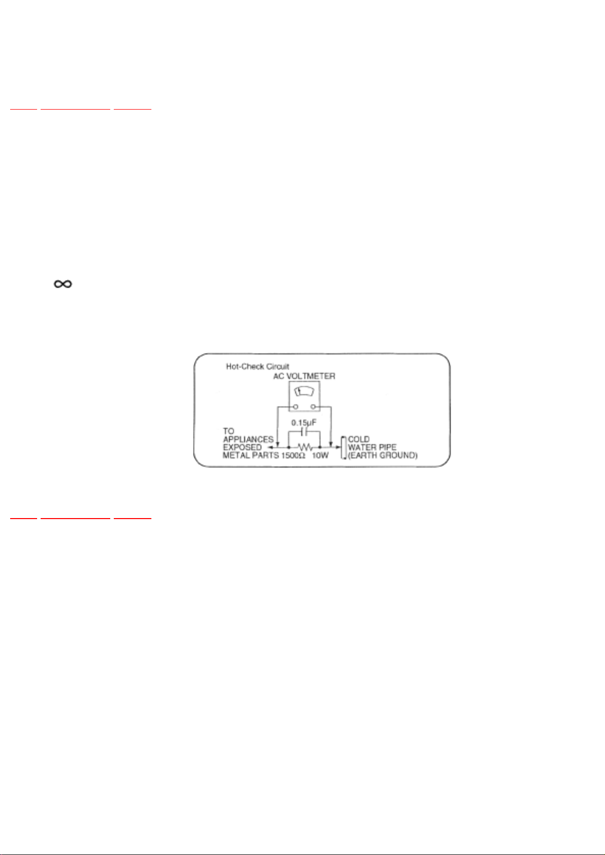
Fig. 1
TOP PREVIOUS NEXT
Page 8

1.1.2 LEAKAGE CURRENT HOT CHECK (See
Figure 1.)
TOP PREVIOUS NEXT
1. Plug the AC cord directly into the AC outlet. Do not use an isolation transformer for this
check.
2. Connect a 1.5kΩ, 10 watts resistor, in parallel with a 0.15μF capacitors, between each
exposed metallic part on the set and a good earth ground such as a water pipe, as shown in
Figure 1.
3. Use an AC voltmeter, with 1000 ohms/volt or more sensitivity, to measure the potential across
the resistor.
4. Check each exposed metallic part, and measure the voltage at each point.
5. Reverse the AC plug in the AC outlet and repeat each of the above measurements.
6. The potential at any point should not exceed 0.75 volts RMS. A leakage current tester
(Simpson Model 229 or equivalent) may be used to make the hot checks, leakage current must
not exceed 1/2 milliamp. In case a measurement is outsideof the limits specified, there is a
possibility of a shock hazard, and the equipment should be repaired and rechecked before it is
returned to the customer.
TOP PREVIOUS NEXT
Page 9

2 Handling the Lead-free Solder
TOP PREVIOUS NEXT
2.1 About lead free solder (PbF)
TOP PREVIOUS NEXT
Page 10

2.1 About lead free solder (PbF)
TOP PREVIOUS NEXT
Distinction of PbF P.C.B. :
P.C.B.s (manufactured) using lead free solder will have a PbF stamp on the P.C.B.
Caution:
● Pb free solder has a higher melting point that standard solder; Typically the melting point is 50
- 70°F (30 - 40°C) higher.
Please use a high temperature soldering iron. In case of the soldering iron with
temperaturecontrol, please set it to 700 ± 20°F (370 ± 10°C).
● Pb free solder will tend to splash when heated too high (about 1100°F/600°C).
● When soldering or unsoldering, please completely remove all of the solder on the pins or
solder area, and be sure to heat the soldering points with the Pb free solder until it melts
enough.
TOP PREVIOUS NEXT
Page 11

3 Before Repair and Adjustment
TOP PREVIOUS NEXT
Disconnect AC power, discharge Power Supply Capacitors C546, C547, C548, C549 through a 10 Ω,
1 W resistor to ground.
DO NOT SHORT-CIRCUIT DIRECTLY (with a screwdriver blade, for instance), as this may
destroy solid state devices.
After repairs are completed, restore power gradually using a variac, to avoid overcurrent.
Current consumption at AC 230V, 50Hz in NO SIGNAL mode should be ~400 mA (E).
Current consumption at AC 230~240V, 50Hz in NO SIGNAL mode should be ~400 mA (EB).
TOP PREVIOUS NEXT
Page 12

4 Protection Circuitry
TOP PREVIOUS NEXT
The protection circuitry may have operated if either of the following conditions are noticed:
● No sound is heard when the power is turned on.
● Sound stops during a performance.
The function of this circuitry is to prevent circuitry damage if, for example, the positive and negative
speaker connection wires are
“shorted”, or if speaker systems with an impedance less than the indicated rated impedance of the
amplifier are used.
If this occurs, follow the procedure outlines below:
1. Turn off the power.
2. Determine the cause of the problem and correct it.
3. Turn on the power once again after one minute.
Note :
When the protection circuitry functions, the unit will not operate unless the power is first turned off
and then on again.
TOP PREVIOUS NEXT
Page 13
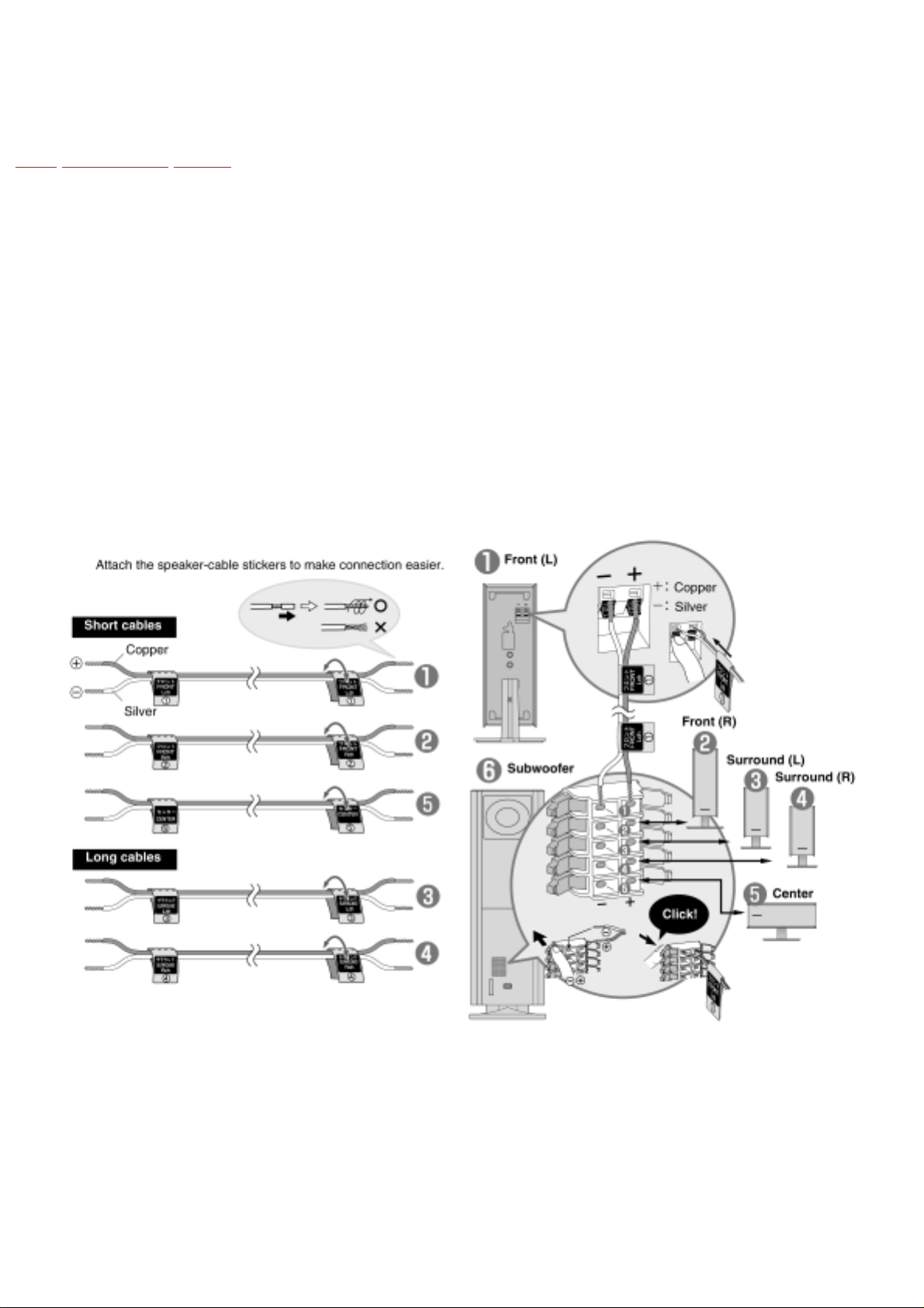
5 Connection of the Speaker Cables
TOP PREVIOUS NEXT
● Be sure to connect speaker cables before connecting the AC power supply cord.
● The load impedance of any speaker used with this unit must be 4Ω.
● Be sure to connect the cable from the right speaker to the right terminal and the cable from the
left speaker to the left terminal.
1. Strip off the outer covering, and twist the center conductor. Make sure the bare ends of the
wires are not unravelled. (If they are, twist them tight again.)
2. Insert the wire to the rear panel of the unit and close the lever.
Notes :
● To prevent damage to circuitry, never short-circuit positive (+) and negative (-) speaker wires.
● Be sure to connect only positive (red) wires to positive (+) terminals and negative (black)
wires to negative (-) terminals.
Page 14

6 Disassembly Procedure
TOP PREVIOUS NEXT
“ATTENTION SERVICER”
Some chassis components may have sharp edges.
Be careful when disassembling and servicing.
1. This section describes procedures for checking the operation of the major printed circuit
boards and replacing the main components.
2. For reassembly after operation checks or replacement, reverse the respective procedures.
Special reassembly procedures are described only when required.
3. Select items from the following index when checks or replacement are required.
Contents
● Disassembly of the Speaker Unit
● Main Component Replacement Procedures
6.1 Disassembly of the Speaker Unit
6.2 Main Component Replacement Procedures
6.2.1 Replacement of the Power IC
TOP PREVIOUS NEXT
Page 15
6.1 Disassembly of the Speaker Unit
TOP PREVIOUS NEXT
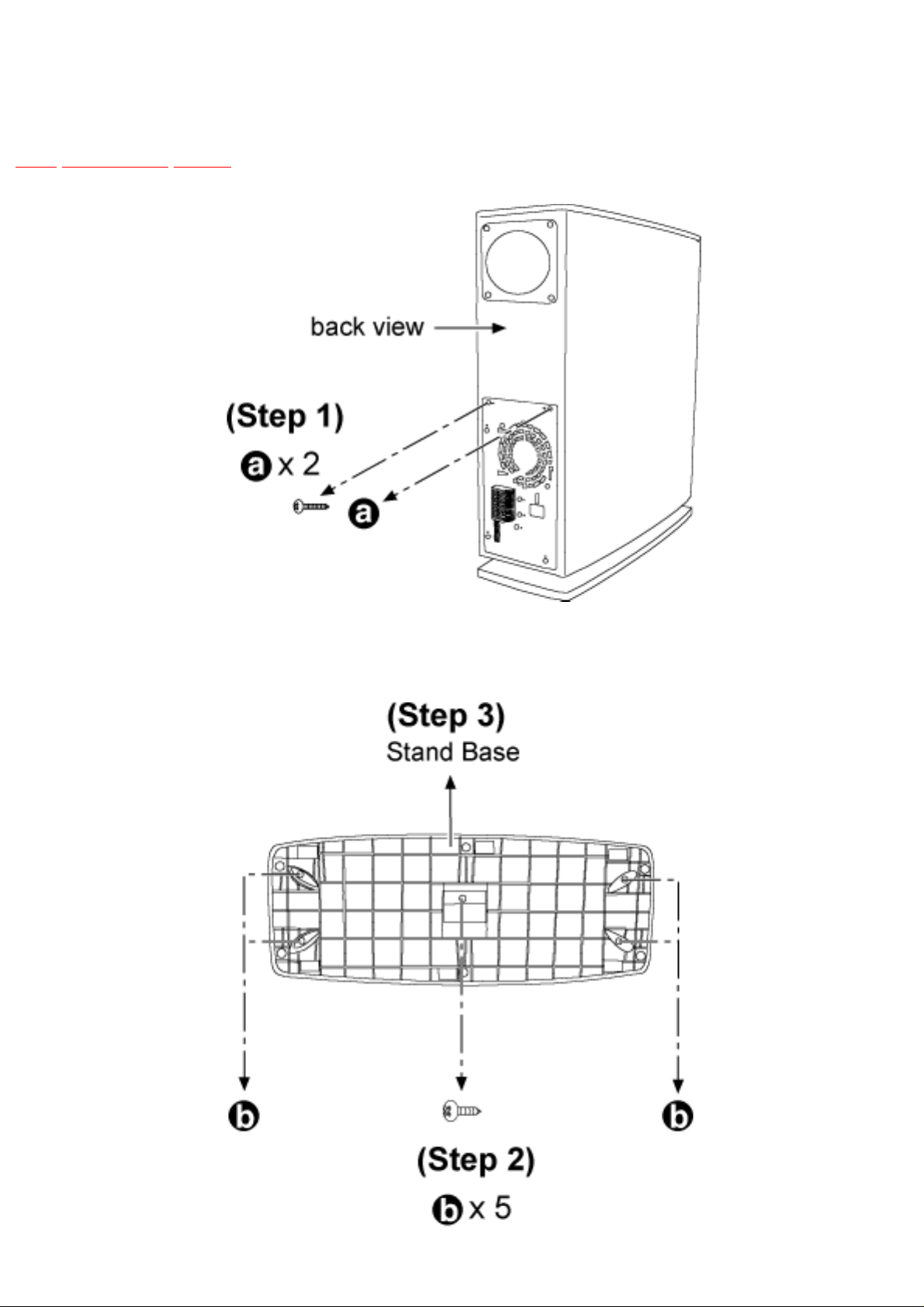
Step 1: Remove 2 screws from the rear panel.
Page 16
Step 2: Remove all screws.
Step 3: Remove the Stand Base.
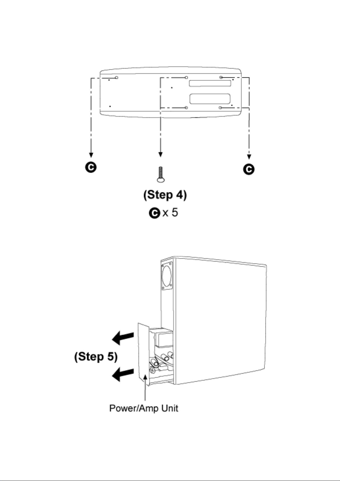
Step 4: Remove 5 screws from the speaker bottom.
Step 5: Pull the Power/Amp Unit as shown.
Page 17
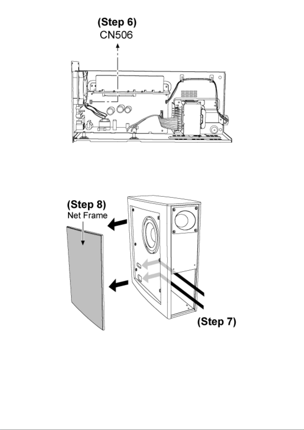
Step 6: Release the connector CN506 and pull out the Power/Amp Unit.
Step 7: Push the Net Frame from two holes inside the unit.
Step 8: Remove the Net Frame.
Page 18
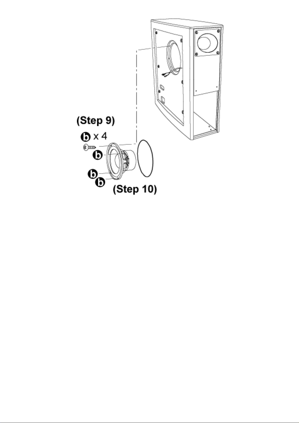
Step 9: Remove all the screws.
Step 10: Remove the Speaker.
Page 19

Step 11 & 12: Remove all the screws.
Page 20

Step 13: Release the connector CN507.
Step 14: Remove the 2 screws.
Step 15 & 16: Remove all the screws.
Page 21

Step 17: Place the Power PCB as shown for checking.
Page 22

Checking for AC Inlet PCB.
TOP PREVIOUS NEXT
Page 23

6.2 Main Component Replacement Procedures
TOP PREVIOUS NEXT
6.2.1 Replacement of the Power IC
TOP PREVIOUS NEXT
Page 24

6.2.1 Replacement of the Power IC
TOP PREVIOUS NEXT
Step 1 & 2: Remove all the screws.
Page 25

Step 3: Desolder the Power IC terminal and replace the component.
TOP PREVIOUS NEXT
Page 26

7 Connection of the Speaker Wiring
TOP PREVIOUS NEXT
TOP PREVIOUS NEXT
Page 27

8 Block Diagram
TOP PREVIOUS NEXT
TOP PREVIOUS NEXT
Page 28

9 Schematic Diagram
TOP PREVIOUS NEXT
(All schematic diagrams may be modified at any time with the development of the new technology)
Note:
● The voltage value and waveforms are the reference voltage of this unit measured by DC
electronic voltmeter (high impedance) and oscilloscope on the basis of chassis. Accordingly,
there may arise some error in voltage values and waveformsdepending upon the internal
impedance of the tester or the measuring unit.
● Importance safety notice :
Components identified by
; mark have special characteristics important for safety.
Furthermore, special parts which have purposes of fire-retardant (resistors), high-quality
sound (capacitors), low-noise (resistors), etc. are used. Whenreplacing any of components, be
sure to use only manufacturer´s specified parts shown in the parts list.
Caution !
IC, LSI and VLSI are sensitive to static electricity.
Secondary trouble can be prevented by taking care during repair.
● Cover the parts boxes made of plastics with aluminium foil.
● Put a conductive mat on the work table.
● Ground the soldering iron.
● Do not touch the pins of IC, LSI or VLSI with fingers directly.
TOP PREVIOUS NEXT
Page 29

10 Printed Circuit Board
TOP PREVIOUS NEXT
TOP PREVIOUS NEXT
Page 30

11 Wiring Connection Diagram
TOP PREVIOUS NEXT
TOP PREVIOUS NEXT
Page 31

12 Illustration of IC’ s, Transistors and Diodes
TOP PREVIOUS NEXT
TOP PREVIOUS NEXT
Page 32

13 Parts Location and Replacement Parts List
TOP PREVIOUS NEXT
Notes:
● Important safety notice:
Components identified by
mark have special characteristics important for safety.
Furthermore, special parts which have purposes of fire-retardent (resistors), high-quality
sound (capacitors), low noise (resistors), etc are used.
When replacing any of these components, be sure to use only manufacturer’s specified parts
shown in the parts list.
● The parenthesized indications in the Remarks columns specify the areas or colour. (Refer to
the cover page for area or colour)
Parts without these indications can be used for all areas.
● Capacitor values are in microfarads (μF) unless specified otherwise, P= Pico-farads (pF), F=
Farads.
● Resistance values are in ohms, unless specified otherwise, 1K=1,000 (OHM).
● The marking (RTL) indicates that the Retention Time is limited for this items. After the
discontinuation of this assembly in production, the item will continue to be available for a
specific period of time. The retention period of a availabilityis dependent on the type of
assembly, and in accordance with the laws governing part and product retention. After the end
of this period, the assembly will no longer be available.
● [M] Indicates in the Remarks columns indicates parts supplied by PAVCSG.
● The “(SF)” mark denotes the standard part.
13.1 Cabinet
13.1.1 Cabinet Parts Location
13.1.2 Cabinet Parts List
Page 33

13.2 Component Parts List
13.3 Packing Materials & Accessories Parts List
13.4 Packaging
TOP PREVIOUS NEXT
Page 34

13.1 Cabinet
TOP PREVIOUS NEXT
13.1.1 Cabinet Parts Location
13.1.2 Cabinet Parts List
TOP PREVIOUS NEXT
Page 35

13.1.1 Cabinet Parts Location
TOP PREVIOUS NEXT
TOP PREVIOUS NEXT
Page 36

13.1.2 Cabinet Parts List
TOP PREVIOUS NEXT
Ref. No. Part No. Part Name & Description Remarks
CABINET AND CHASSIS
1 RFKHBWAMT1PS SPK CABINET ASS’Y [M]
1-1 RMG0520-K CATCH [M]
1-2 XTB4+12AFN SCREW [M]
2 RGK1601-S STAND ORNAMENT [M]
3 RMQ0705 EVA PACKING [M]
4 RKA0147-K FOOT [M]
5 RYB0298AJ NET FRAME ASS’Y [M]
6 XTB4+14AFN SCREW (WOOFER) [M]
7 RGNX0175A-S NAME PLATE LABEL [M]E
7 RGNX0175B-S NAME PLATE LABEL [M]EB
8 REM0072-3 FAN [M]
9 RGR0332A-JA REAR PANEL [M]
10 RHD30092 SCREW (MAIN PCB) [M]
11 RMR1485-W LED HOLDER [M]
12 XTB3+16AFZ SCREW [M]
13 XTB3+20JFZ SCREW [M]
14 XTBS3+8JFZ1 SCREW [M]
15 XTS4+20JFZ SCREW [M]
16 XTW3+15T SCREW [M]
17 XYC26+CJ6FZ SCREW [M]
18 SHE187-6J PCB SUPPORT [M]
19 RMC0158-S TR-FIXTURE [M]
TOP PREVIOUS NEXT
Page 37

13.2 Component Parts List
TOP PREVIOUS NEXT
Ref. No. Part No. Part Name & Description Remarks
PRINTED CIRCUIT BOARD
REP3435F POWER P.C.B./ AC INLET P.C.B./ TRANSFORMER P.C.B./ LED P.C.B. [M]E (RTL)
REP3435G POWER P.C.B./ AC INLET P.C.B./ TRANSFORMER P.C.B./ LED P.C.B. [M]EB (RTL)
INTEGRATED CIRCUITS
IC501 RSN311W64B-P IC HIC [M]
IC502 C0AABB000055 IC AMP [M]
TRANSISTORS
Q501 KTC3199GRTA TRANSISTOR [M]
Q502 KTC3199GRTA TRANSISTOR [M]
Q503 KTC3199GRTA TRANSISTOR [M]
Q505 KTC3199GRTA TRANSISTOR [M]
Q506 KRA102MTA TRANSISTOR [M]
Q507 KTC3199GRTA TRANSISTOR [M]
Q508 KTA12710YTA TRANSISTOR [M]
Q509 KTC3199GRTA TRANSISTOR [M]
Q510 KTC3199GRTA TRANSISTOR [M]
Q511 KTC2026 TRANSISTOR [M]
Q513 KTC3199GRTA TRANSISTOR [M]
Q514 KTC3199GRTA TRANSISTOR [M]
Q515 KTC3199GRTA TRANSISTOR [M]
Q516 KRC102MTA TRANSISTOR [M]
Q517 KTC2026 TRANSISTOR [M]
Q519 KTC3199GRTA TRANSISTOR [M]
Q520 KRA102MTA TRANSISTOR [M]
DIODES
Page 38

D500 B0AACK000004 DIODE [M]
D501 B0JAPG000019 DIODE [M]
D502 B0JAPG000019 DIODE [M]
D503 MA2C700A0F DIODE [M]
D504 B0AACK000004 DIODE [M]
D505 B0AACK000004 DIODE [M]
D506 B0AACK000004 DIODE [M]
D507 B0AACK000004 DIODE [M]
D508 B0AACK000004 DIODE [M]
D509 B0BA5R100013 DIODE [M]
D510 B0BA9R600002 DIODE [M]
D511 B0HARM000017 DIODE [M]
D512 B0HARM000017 DIODE [M]
D513 B0HARM000017 DIODE [M]
D514 B0HARM000017 DIODE [M]
D515 B0EAKM000085 DIODE [M]
D516 B0EAKM000085 DIODE [M]
D517 B0HARM000017 DIODE [M]
D518 B0HARM000017 DIODE [M]
D519 B0AACK000004 DIODE [M]
D524 SLI325URCT31 DIODE [M]
D525 B0BA6R600008 DIODE [M]
D527 B0EAKM000085 DIODE [M]
D528 B0EAKM000085 DIODE [M]
D529 B0EAKM000085 DIODE [M]
D530 B0EAKM000085 DIODE [M]
D533 B0BA5R100013 DIODE [M]
CONNECTORS
CN501 K1FB125B0095 SYSTEM CONNECTOR [M]
CN502 K1KB07B00020 2P CONNECTOR [M]
CN503 K1KA12A00066 CONNECTOR [M]
CN506 K1KA03A00006 CONNECTOR [M]
CN507 K1KA02A00008 CONNECTOR [M]
Page 39

CP502 K1KA07A00123 2P CONNECTOR [M]
COILS & TRANSFORMERS
L500 RLQZ371 LINE FILTER [M]
L501 G0AR76Y00001 CHOKE COIL [M]
L502 G0AR76Y00001 CHOKE COIL [M]
L503 G0AR76Y00001 CHOKE COIL [M]
L504 G0AR76Y00001 CHOKE COIL [M]
L505 G0AR76Y00001 CHOKE COIL [M]
T501 ETP76VSU62CA POWER TRANSFORMER [M]
T502 G4C2AAJ00005 BACK-UP TRANSFORMER [M]
COMPONENT COMBINATION
Z501 ERZV10V511CS ZENER [M]
RELAY
RLY501 RSY0040M-0 PRIMARY RELAY [M]
SPEAKER
SP1 EAST17PL21A6 SPEAKER
FUSES
F1 K5D202BK0005 250V 2A FUSE [M]
FUSE HOLDERS
FC501 EYF52BC FUSE HOLDER [M]
FC502 EYF52BC FUSE HOLDER [M]
FUSE PROTECTOR
FP1 K5G502AA0002 5A FUSE PROTECTOR [M]
Page 40

HOLDERS
H500 K1YF12000002 12P WIRE HOLDER [M]
H505A RMR0312 3P CABLE HOLDER [M]
H505B RMR0312 3P CABLE HOLDER [M]
WIRES
W1 REE1205 WIRE UNIT [M]
W2 REE1204 WIRE UNIT [M]
W500 REX1146 WIRE UNIT [M]
W505 RWJ1103320XX 3P STRAND WIRE [M]
JACKS
JK500 K2AA2B000004 JK AC INLET [M]
JK501 K4BC06B00027 JK 6P SPEAKER [M]
JK502 K4BC04B00056 JK 4P SPEAKER [M]
EARTH TERMINAL
E500 K4CZ01000027 TERMINALS [M]
E501 K4CZ01000027 TERMINALS [M]
RESISTORS
R401 ERDS2TJ224T 220K 1/4W [M]
R402 ERDS2TJ102T 1K 1/4W [M]
R403 ERDS2TJ104T 100K 1/4W [M]
R501 ERDS2TJ472T 4.7K 1/4W [M]
R502 ERDS2TJ472T 4.7K 1/4W [M]
R503 ERDS2TJ153T 15K 1/4W [M]
R504 ERDS2TJ153T 15K 1/4W [M]
R505 ERDS2TJ153T 15K 1/4W [M]
R506 ERDS2TJ153T 15K 1/4W [M]
R507 ERDS2TJ392T 3.9K 1/4W [M]
R508 ERDS2TJ392T 3.9K 1/4W [M]
Page 41

R509 ERDS2TJ472T 4.7K 1/4W [M]
R510 ERDS2TJ472T 4.7K 1/4W [M]
R511 ERDS2TJ153T 15K 1/4W [M]
R512 ERDS2TJ153T 15K 1/4W [M]
R513 ERDS2TJ563T 56K 1/4W [M]
R514 ERDS2TJ563T 56K 1/4W [M]
R515 ERDS2TJ563T 56K 1/4W [M]
R516 ERDS2TJ563T 56K 1/4W [M]
R517 ERDS2TJ563T 56K 1/4W [M]
R518 ERDS2TJ563T 56K 1/4W [M]
R519 ERDS2TJ824T 820K 1/4W [M]
R520 ERDS2TJ223T 22K 1/4W [M]
R521 ERDS2TJ103T 10K 1/4W [M]
R522 ERDS2TJ273T 27K 1/4W [M]
R523 ERDS2TJ124T 120K 1/4W [M]
R524 ERDS2TJ124T 120K 1/4W [M]
R525 ERDS2TJ154T 150K 1/4W [M]
R526 ERDS2TJ124T 120K 1/4W [M]
R527 ERDS2TJ124T 120K 1/4W [M]
R528 ERDS2TJ154T 150K 1/4W [M]
R529 ERDS2TJ223T 22K 1/4W [M]
R530 ERD25FVJ1R0T 1 1/4W [M]
R531 ERD25FVJ1R0T 1 1/4W [M]
R532 ERDS2TJ472T 4.7K 1/4W [M]
R533 ERDS1FVJ100T 10 1/2W [M]
R534 ERDS1FVJ100T 10 1/2W [M]
R535 ERDS1FVJ100T 10 1/2W [M]
R536 ERDS1FVJ100T 10 1/2W [M]
R537 ERDS1FVJ100T 10 1/2W [M]
R538 ERDS1FVJ100T 10 1/2W [M]
R539 ERDS2TJ101T 100 1/4W [M]
R540 ERDS2TJ101T 100 1/4W [M]
R541 ERDS2TJ101T 100 1/4W [M]
R542 ERDS2TJ101T 100 1/4W [M]
R543 ERDS2TJ101T 100 1/4W [M]
R544 ERDS2TJ101T 100 1/4W [M]
R545 ERDS2TJ224T 220K 1/4W [M]
Page 42

R546 ERDS2TJ102T 1K 1/4W [M]
R547 ERDS2TJ394T 390K 1/4W [M]
R548 ERDS2TJ334T 330K 1/4W [M]
R549 ERDS2TJ473T 47K 1/4W [M]
R550 ERDS2TJ103T 10K 1/4W [M]
R551 ERDS2TJ472T 4.7K 1/4W [M]
R552 ERDS2TJ562T 5.6K 1/4W [M]
R553 ERDS2TJ563T 56K 1/4W [M]
R554 ERDS2TJ824T 820K 1/4W [M]
R555 ERDS2TJ104T 100K 1/4W [M]
R556 ERDS2TJ103T 10K 1/4W [M]
R557 ERDS2TJ563T 56K 1/4W [M]
R558 ERDS1FVJ180T 18 1/2W [M]
R559 ERDS2TJ563T 56K 1/4W [M]
R560 ERDS2TJ103T 10K 1/4W [M]
R561 ERDS2TJ101T 100 1/4W [M]
R565 ERDS1FVJ392T 3.9K 1/2W [M]
R566 ERDS2TJ271T 270 1/4W [M]
R567 ERDS1FVJ152T 1.5K 1/2W [M]
R568 ERDS2TJ151T 150 1/4W [M]
R569 ERDS1FVJ392T 3.9K 1/2W [M]
R570 ERDS2TJ103T 10K 1/4W [M]
R571 ERDS2TJ332T 3.3K 1/4W [M]
R572 ERDS2TJ223T 22K 1/4W [M]
R573 D0XGR10JA005 10 1/10W [M]
R575 ERDS2TJ682T 6.8K 1/4W [M]
R577 ERDS2TJ152T 1.5K 1/4W [M]
R578 ERDS2TJ103T 10K 1/4W [M]
R579 ERDS2TJ332T 3.3K 1/4W [M]
R580 ERDS2TJ220T 22 1/4W [M]
R581 ERDS2TJ100T 10 1/4W [M]
R582 ERDS2TJ100T 10 1/4W [M]
R583 ERDS2TJ100T 10 1/4W [M]
R584 ERDS2TJ100T 10 1/4W [M]
R585 ERDS2TJ100T 10 1/4W [M]
R587 ERDS2TJ272T 2.7K 1/4W [M]
R588 ERDS2TJ151T 150 1/4W [M]
Page 43

R589 ERDS2TJ103T 10K 1/4W [M]
R590 ERDS2TJ102T 1K 1/4W [M]
R591 ERDS2TJ682T 6.8K 1/4W [M]
R592 ERDS2TJ683T 68K 1/4W [M]
R593 ERDS2TJ474T 470K 1/4W [M]
R594 ERDS2TJ103T 10K 1/4W [M]
R595 ERDS2TJ101T 100 1/4W [M]
R596 ERDS2TJ473T 47K 1/4W [M]
R597 ERDS2TJ103T 10K 1/4W [M]
R598 ERDS1FVJ152T 1.5K 1/2W [M]
R599 ERDS2TJ223T 22K 1/4W [M]
CAPACITORS
C500 ECKWRS102MBC 1000P 400V [M]
C501 ECBT1H102KB5 1000P 50V [M]
C502 ECBT1H102KB5 1000P 50V [M]
C503 ECBT1H102KB5 1000P 50V [M]
C504 ECBT1H681KB5 680P 50V [M]
C505 ECBT1H102KB5 1000P 50V [M]
C506 ECBT1H102KB5 1000P 50V [M]
C507 ECBT1H180JC5 18P 50V [M]
C508 ECBT1H180JC5 18P 50V [M]
C509 ECBT1H220JC5 22P 50V [M]
C510 ECBT1H220JC5 22P 50V [M]
C511 ECBT1H220JC5 22P 50V [M]
C512 ECBT1H220JC5 22P 50V [M]
C513 F1D1H473A012 0.047 50V [M]
C514 ECA0JM101B 100 6.3V [M]
C515 ECKR2H103ZF5 0.01 500V [M]
C516 ECKR2H103ZF5 0.01 500V [M]
C517 ECBT1C103NS5 0.01 16V [M]
C518 F1D1H473A012 0.047 50V [M]
C519 F1D1H473A012 0.047 50V [M]
C520 F1D1H473A012 0.047 50V [M]
C521 F1D1H473A012 0.047 50V [M]
C522 F1D1H473A012 0.047 50V [M]
Page 44

C523 F1D1H473A012 0.047 50V [M]
C524 F1D1H1040002 0.1 50V [M]
C525 F1D1H1040002 0.1 50V [M]
C526 F1D1H1040002 0.1 50V [M]
C527 F1D1H1040002 0.1 50V [M]
C528 F1D1H473A012 0.047 50V [M]
C529 F1D1H1040002 0.1 50V [M]
C530 ECBT1H102KB5 1000P 50V [M]
C531 ECBT1H102KB5 1000P 50V [M]
C532 ECBT1H102KB5 1000P 50V [M]
C533 ECBT1H102KB5 1000P 50V [M]
C534 ECA1HM330B 33 50V [M]
C536 ECEA1CKA330B 33 16V [M]
C537 F1D1H1040002 0.1 50V [M]
C538 ECA0JM101B 100 6.3V [M]
C539 ECEA0JKA221B 220 6.3V [M]
C540 ECEA1HKA2R2B 2.2 50V [M]
C541 ECEA1CKA100B 10 16V [M]
C543 ECBT1H102KB5 1000P 50V [M]
C544 ECA1HM101B 100 50V [M]
C545 F1D1H1040002 0.1 50V [M]
C546 ECA1VM332B 3300 35V [M]
C547 ECA1VM472B 4700 35V [M]
C548 ECA1VM472B 4700 35V [M]
C549 ECA1VM332B 3300 35V [M]
C550 ECBT1C103NS5 0.01 16V [M]
C551 ECBT1H103KB5 0.01 50V [M]
C552 F1D1H1040002 0.1 50V [M]
C553 ECQE1104KF3 0.1 100V [M]
C554 ECQE1104KF3 0.1 100V [M]
C555 ECEA1VKA4R7B 4.7 35V [M]
C556 ECBT1H103KB5 0.01 50V [M]
C557 ECEA1CKA220B 22 16V [M]
C558 ECA1CM102B 1000 16V [M]
C559 ECBT1H103KB5 0.01 50V [M]
C560 ECA1HM100B 10 50V [M]
C561 ECEA1HKA2R2B 2.2 50V [M]
Page 45

C562 ECQB1H562JF3 5600P 50V [M]
C563 ECQV1H823JL3 0.082 50V [M]
C564 ECBT1C122KR5 1200P 16V [M]
C565 F1D1H1040002 0.1 50V [M]
C566 F1D1H1040002 0.1 50V [M]
C567 ECA1HM100B 10 50V [M]
C568 ECBT1C103NS5 0.01 16V [M]
C569 F1D1H473A012 0.047 50V [M]
TOP PREVIOUS NEXT
Page 46

13.3 Packing Materials& Accessories Parts List
TOP PREVIOUS NEXT
Ref. No. Part No. Part Name & Description Remarks
PACKING MATERIALS
P1 RPF0357 MIRAMAT (STAND) [M]
P2 RPNX0189 POLYFOAM [M]
P3 RPFX0045 MIRAMAT (S.WOOFER) [M]
TOP PREVIOUS NEXT
Page 47

13.4 Packaging
TOP PREVIOUS
TOP PREVIOUS
Page 48

Page 49

Page 50

C0AABB000055
5
RSN311W64B-P
KTA12710YTA
KTC3199GRTA
KRA102MTA
KRC102MTA
8
KTC2026
E
C
B
B0EAKM000085
B0JAPG000019
Ca
A
Anode
1
Cathode
4
1
..................
26
MA2C700A0F
Ca
Cathode
A
Anode
B0BA6R600008
E
C
B
B0HARM000017
Ca
Cathode
A
Anode
SLI325URCT31
B0BA9R600002
B
C
E
B0AACK000004
B0BA5R100013
A
Anode
Ca
Cathode
Anode
Cathode
ACa
Page 51

CN501
25
24
.
.
.
.
.
.
.
.
.
.
.
.
.
TO MAIN UNIT
2
1
C
JK502
SR
SL
SPEAKERS
FR
FL
JK501
CN507
2
1
1
2
3
CN506
POWER P.C.B.
7. . . . . .1
CP502
FAN
-
+
1
.
.
.
.
.
.
.
12
H500/W500
SPEAKER
WOOFER
SOLDER SIDE
BLU
PbF
12
.
.
.
.
.
.
.
1
CN503
3
2
1
H505B/W505
W1
W2
BRW
LED P.C.B.
PbF
1
2
3
H505A/W505
SOLDER SIDE
AC IN
230~240V
50HZ
T501(POWER TRANSFORMER)
TRANSFORMER
JK500
SOLDER SIDE
PbF
P.C.B.
T502(POWER TRANSFORMER)
CN502
7. . . . . .1
W2
BLU
AC INLET
P.C.B.
SOLDER SIDE
W1
BRW
PbF
Page 52

ABCDEFG
6
D506
1
POWER P.C.B. (REP3435F...E)
(REP3435G...EB)
2
CAUTION
RISK OF ELECTRIC SHOCK
AC VOLTAGE LINE. PLEASE DO NOT
TOUCH THIS P.C.B
3
CN501
25
24
23
22
21
20
19
18
17
16
15
14
13
JK502
12
11
10
9
8
7
6
5
4
3
2
1
4
TO MAIN UNITSPEAKERS
5
C
SR
SL
6
FR
C525
FL
JK501
7
C528
C524
J591
C519
C527
C526
R536
J592
C532
C522
C518
C521
L503
R583
J570
J528
R543
R544
R540
R539
R537
R533
-
+
CN507
C531
R534
C520
J519
C530
R581
L501
R584
L504
J571
R585
L505
R582
L502
J410
+
PbF
J572
1
2
3
R535
J521
E500
J575
CN506
C533
J574
R573
C552
C549
R593
R597
C565
C561
J409
J595
C563
C566
5678
IC502
R403
R591
J573
J593
J594
R592
J581
C550
J596
1234
C564
CP502
7654321
R542
R522
R521
R545
C529
D504
J538
J531
C562
R538
R595
R596
R594
C569
C523
J539
R547
D503
R531
R530
J536
J597
J533
C534
C548
J504
R548
Q505
R541
R549
J577
J537
J550
15
IC501
B
C
E
D501
R572
Q506
B
C
E
J563
J562
J511
J599
J561
Q513
EB
C
EB
C
Q514
R599
J517
J515
J565
R565
J576
10
R571
J579
J532
D508
C568
J598
J580
J514
D507
Q509
J507
J508
R554
R555
C540
R557
B
C
J408
E
C539
D516
D515
C547
R529
C545
R519
C513
C517
D502
15 20
J506
D518
C537
R556
Q510
J552
J564
C505
Q507
B
C
R559
R553
E
R561
B
B
C
C
E
R552
R523
C515
J509
C546
R501
J510
C516
C504
E
Q508
R513
C507
C503
C50
R551
R524
8
9
Page 53

R555
J408
J508
C540
D516
C539
R554
R557
D515
R556
J506
D518
C537
Q510
J552
HG
Q507
B
C
R559
R553
E
R561
D506
R551
R560
C536
D505
R550
D512
J586
B
B
C
C
E
E
J509
Q508
R552
C546
J587
J588
C538
D519
R558
J512
R570
D511
IJKLM
J582
J583
J566
FP1
J505
J513
5A
CN503
12
11
10
9
8
7
6
5
4
3
2
1
J418
R402
D514
R566
J567
J568
J569
J560
C541
EB
C
Q520
D513
C514
J535
R546
J548
B
C
E
Q501
D517
J547
J401
J546
J589
R520
C554
C553
J545
B
C
E
J544
Q502
J402
J403
J404
J405
J406
J564
C545
R519
02
520 26
C517
C505
R523
C515
R501
J510
C516
C504
R513
C507
C503
C506
J584
Q503
EB
R514
R524
C
C508
R516
R526
C502
C501
C510
R532
R525
J518
R515
R510
R509
C509
R527
R517
R575
C511
R528
R518
R512
J417
R502
R504
R508
R507
R506
C543
Q511
B
R568
J541
C
R503
E
J590
R505
C512
R511
R569
D510
J551
J516
J585
R598
R567
C544
C567
C551
D533
D509
C560
H505B/W505
E501
3
2
1
Page 54

SCHEMATIC DIAGRAM-1
POWER CIRCUIT
: -B SIGNAL LINE
: +B SIGNAL LINE
: MAIN SIGNAL LINE
TO
MAIN CIRCUIT
(JK700) OF
SA-HT500E/EB/EG-S,
SA-ST1EB/EG-S
CN501
10
11
12
13
14
15
16
17
18
19
20
21
22
23
24
25
E501
K4CZ01000027
AC1
1
DC_DET
2
AC2
3
SYS6V
4
HP_CNT
5
D.GND
6
FL
7
HELP
8
A.GND
9
A.GND
FR
SL
A.GND
SR
C
A.GND
SW
A.GND
PCONT
MUTE A/CNTR SURR
SYNC
FL1
AC3
FL2
AC4
C551
0.01
R501
4.7K
R502
4.7K
R506
15K
R505
15K
R539 100
R540 100
R543 100
IC501
FLin
FRin
IN GND
SUBin
Cin
-VD
+VD
SRin
SLin
RELAY
-Di SENS
+Di SENS
IH DET
R532
4.7K
R546
1K
Q506
Q505
SWITCHING
C538
R558
18
DISP HMUT
R523
820K
R519
R557
56K
120K
R520
R530 1
R531 1
26 25 24 23 22 21 20 19 18 17 16 15 14 13 12 11 10 9
R513
56K
C507 18P
R514 56K
C508 18P
C505 1000P
C506 1000P
R516 56K
C501
1000P
R507
3.9K
R503
15K
R504
15K
R541
100
R542
100
MA2C700A0F
C529 0.1
3.9K
R508
D503
R547
390K
R549 47K
C502
1000P
C503
1000P
R509
4.7K
R511
15K
R512
15K
R544
100
B0AACK000004
C534
50V33
R553
56K
R550
10K
C536
16V33
C504 680P
R510 4.7K
C516
0.01
R402
1K
D504
C510 22P
R515 56K
C509 22P
R517 56K
C511 22P
R518 56K
C512 22P
C515
0.01
C517
0.01
KRA102MTA
INTERFACE SWITCH
R545
220K
D503
R548
330K
Q507
KTC3199GRTA
SWITCH
Q507
R561
100
D506
10K
D505
R560
C513
0.047
Q520
KRA102MTA
INTERFACE SWITCH
KTC3199GRTA
6.3V100
R559
56K
SL_O
R526
120K
R525
150K
R527
120K
R528
22K
Q503
6.3V220
SR_O
R524
120K
150K
C539
GND
C514
6.3V100
AC IN
C_O
-VCC LOW
+VCC LOW
8
6 5
7
D502
D501
R529
22K
Q503
KTC3199GRTA
SWITCH
Q502
Q501
Q509
KTC3199GRTA
SWITCH
D505-D506
B0AACK000004
SUB_O
-VCC HI
+VCC HI
432
FR_O
FL_O
1
27K
R522
D508
B0AACK000004
RSN311W64B-P
POWER HIC
D501-D502
B0JAPG000019
R521
10K
Q501-Q502
KTC3199GRTA
SWITCH
IC501
TO FAN
CN507
16V10
D507
C541
R566
270
D507, D519
B0AACK000004
D519
R551
4.7K
R554 820K
C537 0.1
R552
5.6K
Q508
+
1
-
2
Q508
KTA12710YTA
CURRENT AMP
Q510
KTC3199GRTA
SWITCH
Q510
R556
10K
R555
100K
C540
50V2.2
Page 55

L501
R581 10
L502
R582 10
L505
R585 10
L503
R583 10
L504
R584 10
L501-L505
G0AR76Y00001
SCHEMATIC DIAGRAM-2
POWER CIRCUIT
R593
R591
470K
6.8K
C562
5600P
C563
0.082
C561
R575
50V2.2
6.8K
Q513
KTC3199GRTA
DC DETECT SWITCH
KTC3199GRTA
DC DETECT SWITCH
: -B SIGNAL LINE
: +B SIGNAL LINE
C564
1200P
R592
IC502
C522
0.047
C518
0.047
R533
68K
10
C523
0.047
C569
0.047
10
C565
0.1
C0AABB000055
DUAL LOW-NOISE OP AMP
5 6 7 8
Q514
C520
C521
0.047
0.047
R53510R53610R53710R538
R597
1234
10K
R403
100K
R594 10K
0.1
C566
C519
0.047
R596
R534
47K
10
C552
0.1
: MAIN SIGNAL LINE
C568
0.01
C524
0.1
Q514
R599
22K
R571
3.3K
C526
0.1
C525
0.1
C528
0.047
C527
Q513
0.1
R572
22K
R595
100
R573
0.1
JK501
+
FLch
-
+
FRch
-
+
SRLch
-
JK502
+
SRRch
-
+
CENTER
-
3
2
SUB WOOFFER
1
CN506
C560
50V10
Q511
KTC2026
VOLTAGE REGULATOR
C544
50V100
D509
C543
1000P
C567
50V10
D509, D533
B0BA5R100013
R568
150
D533
R569
3.9K
D510
B0BA9R600002
R598
1.5K
R567
1.5K
C545
0.1
R570
10K
D515
C546
35V3300
D517
D515, D516
B0EAKM000085
C547
35V4700
D513
D514
D511-D514,D517-D518
B0HARM000017
C530
1000P
C550
0.01
C548
35V4700
D511
D512
R565
3.9K
C531
1000P
E500
K4CZ01000027
D516
C549
35V3300
C532
1000P
D518
C554
0.1
C553
0.1
FP1
K5G502AA0002
C533
1000P
PCONT
SYS6V
3
3
2
2
1
1
H505B/W505
FP1
1
2
GND
3
SYNC
4
5
HELP
6
7
D524
SLI325URCT31
H505A/W505
1
2
3
4
5
6
7
8
9
10
11
12
CP502
TO
AC INLET
CIRCUIT
(CN502) ON
SCHEMATIC
DIAGRAM-3
R577
1.5K
LED
CIRCUIT
CN503
TO
TRANSFORMER
CIRCUIT
(H500/W500) ON
SCHEMATIC
DIAGRAM-3
Page 56

SCHEMATIC DIAGRAM-3
: -B SIGNAL LINE
: +B SIGNAL LINE
H500/W500
TO
POWER CIRCUIT
(CN503) ON
SCHEMATIC
DIAGRAM-2
D530
D529
D527-D530
B0EAKM000085
C559
0.01
R578
10K
C555
35V4.7
D528
D527
TO
POWER CIRCUIT
(CP502) ON
SCHEMATIC
DIAGRAM-2
CN502
R589
10K
Q516
KRC102MTA
SYNC SWITCH
1
PCONT
2
GND
3
SYNC
4
SYS6V
5
HELP
6
7
R590
1K
R580
22
Q517
KTC2026
VOLTAGE REGULATOR
C557
16V22
R401
220K
R579
3.3K
C556
0.01
R587
2.7K
R588
150
D525
D525
B0BA6R600008
C558
16V1000
TRANSFORMER CIRCUIT
Q519
KTC3199GRTA
DC DET SWITCH
W1
T501
ETP76VSU62CA
1
2
3
4
5
6
7
8
9
10
11
12
FOR E/EG
FOR EB
W2
Q515
Q515
KTC3199GRTA
DC DET SWITCH
D500
B0AACK000004
D500
T502
G4C2AAJ00005
RLY501
RSY0040M-0
4 3
2 1
C500
1000P
AC INLET CIRCUIT
Z501
ERZV10V511CS
F1
250V T2AL
FC502
FC501
L500
RLQZ371
JK500
AC IN
230V-240V
50HZ
Page 57

POWER CONTROL
CIRCUIT
IC501
RSN311W64B-P
-
+
-
+
-
+
-
+
POWER CONTROL/PROTECTION CIRCUIT
POWER HIC
TO MAIN
BLOCK
(JK700) OF
SA-HT500E/EB/EG-S,
SA-ST1EB/EG-S
A
SL(R)
CCH
FL(R)
DC_DET
SUBWO
HP_CNT
AC1(4)
AC2(5)
26
(25)
FLIN(R)
CIN
SUBIN
22 23 18
SLIN(R)
+DI SENS
2015 3 6 1
(19)
B
D508
IC502
C0AABB000055
DUAL
LOW-NOISE
OP AMP
INTERFACE
+VD
B B
Q520
SWITCH
+VCC HI
+VCC LOW
D501
FILTER
FILTER
FILTER
FILTER
Q513,
Q514
FL_O(R)
(2)
DC DET
SWITCH
Q503
SWITCH
C_O
8 512(11) 24
Q501,
Q502
SWITCH
Q507~Q510
FAN
MOTOR
DRIVE
SL_O(R)
M
B
Q511
VOLTAGE
REGULATOR
FILTER
FILTER
FILTER
SUB_O
B
B
IN GND
B
Q506
INTERFACE
SWITCH
Q505
SWITCHING
D513~D515,
D517
D511,D512,
D516,D518
DISP HMUT
IH DET
AC IN
91314 7421
TO FL
DISPLAY
-VCC LOW
D502
-VCC HI
-VD
B B
T501
POWER TRANSFORMER
-DI SENS
16
JK501(JK502)
SURROUND
SPEAKER
JK502
CENTRE
SPEAKER
SUBWOOFER
JK501
FRONT
SPEAKER
RLY501
B
PCONT
SYNC
Q515,Q519
DCDET
SWITCH
B
Q517
VOLTAGE
REGULATOR
B
D527~D530
Q516
SYNC
SWITCH
SIGNAL LINES
: MAIN SIGNAL LINE
( ) Indicates Pin No. of Right Channel Note : Signal Lines are applicable to the Left Channel only.
T502
SUB
TRANSFORMER
Z501
JK500
AC INLET
L500
F1
E500
Page 58

ABCDEFG
1
AC INLET P.C.B. (REP3435F...E)
(REP3435G...EB)
CAUTION
RISK OF ELECTRIC SHOCK
2
3
JK500
AC IN
230V-240V
50HZ
4
J500
J501
J502
J503
AC VOLTAGE LINE. PLEASE DO NOT
TOUCH THIS P.C.B
FC501
F1 250V T2AL
L500
PbF
T502 (POWER TRANSFORMER)
J525
J526
7
J540
CN502
FC502
W2
W1
C558
C555
BRWBLU
C557
Q517
E
R587
C
C556
R588
D525
B
Z501
C500
RLY501
2
1
R590
34
R579
D500
J523
R401
1
J522
J529
Q515
Q516
EB
C
R589
R578
B
C
Q519
E
D527
C559
J527
R580
D529
D530
D528
B
C
E
5
TRANSFORMER P.C.B. (REP3435F...E)
(REP3435G...EB)
6
CAUTION
RISK OF ELECTRIC SHOCK
AC VOLTAGE LINE. PLEASE DO NOT
TOUCH THIS P.C.B
LED P.C.B.(REP3435F...E)
W1W2
BRW
7
1
J520
2
3
4
5
6
7
H500/W500
8
8
9
10
11
12
BLU
R577
D524
PbF
(REP3435G...EB)
3
2
1
H505A
/W505
9
T501 (POWER TRANSFORMER)
PbF
 Loading...