

Page 1
SERVICE MANUAL
ANAM
DVD RW/VCR-RECORDER
CONTENTS
Specifications
Disassembly
Principal Parts Location
Troubleshooting
Electrical Parts List
IC Internal Diagrams
IC and Transistor Voltage Chart
VCR Mechanism
Adjustment Method
Exploded View
Block Diagram
Wiring Diagram
Schematic Diagrams
Printed Circuit Boards
---------------------------------------- 2
------------------------------------------- 6
-------------------------- 7
------------------------------------- 8
-------------------------------- 11
----------------------------- 58
---------------------------------- 98
---------------------------- 103
----------------------------------- 106
----------------------------------- 110
---------------------------------- 112
--------------------------- 114
-------------------------- 132
------------- 90
Page 2

SPECIFICATIONS
DVD Audio Section VCR Audio Section [Hi-Fi]
Single-Noise (1 KHz)
Channel Separation (1 KHz)
Total Harmonic Distortion
TV TUNER Section
Audio Output Level (Mono) 100.25MHz
T.H.D (Mono) 100.25MHz
Composite Output Level 100.25MHz
DVD VIDEO Section (MDVD-111)
Composite
S-Video Y Level
RGB
Component
CVBS Level
C Level
R Level
G Level
B Level
Y Level
Pb Level
Pr Level
DVD +RW Playability Section
Eccentric TDV-PW 512CW
Vertical Deviation(skew)TDV-PW 532CW
Scratch TDV-PW 521CW
ギ90dB
ギ85dB
0.1%
550mV
0.2%
1V(p-p)
1V(p-p)
1V(p-p) 1.0±0.2V
286mV(p-p) 0.3±0.03V
700mV(p-p) 0.3±0.03V
700mV(p-p) 1.0±0.2V
700mV(p-p)
1V(p-p)
700mV(p-p) 45W
700mV(p-p) 6.8Kg
±100䶦
0.6mm(p-p)
1mm
Output Level
Audio-8dBm (E.E)
-8±2dBm
Distortion(T.H.D)
Audio-8dBm (SP)
Audio-8dBm (LP/SLP)
S/N Ration
Audio-8dBm (E.E)
Audio-8dBm (SP)
Audio-8dBm (LP/SLP)
VCR Video Section
E.E Video Level
SRP SYNC Level
SRP BURST Level
SRP Video Level
GENERAL
Power Consumption
Weight (Main unit)
Dimension (WዖHዖD) 430ዖ109.3ዖ410.4mm
ײ 1.5 %
ײ 2 %
䮭52%
䮭50%
䮭50%
DVD -RW Playability Section
Eccentric TDV-MW 512CW
Vertical Deviation(skew)TDV-MW 532CW
Scratch TDV-MW 521CW
±140䶦
0.6mm(p-p)
0.7mm
DVD +RW/-RW Recording Playability Section
Composite
S-Video Y Level
RGB R Level
Scart
Composite
CVBS Level
C Level
G Level
B Level
CVBS Level 1V(p-p)
Y Level
Pb Level
Pr Level
1V(p-p)
1V(p-p)
286mV(p-p)
700mV(p-p)
700mV(p-p)
700mV(p-p)
1V(p-p)
700mV(p-p)
700mV(p-p)
NOTE : Design and specifications are subject to change and improvement without notice
- 2 -
Page 3
- 3 -
SAFETY PRECAUTIONS
The following check should be performed for the continued
protection of the customer and service technician.
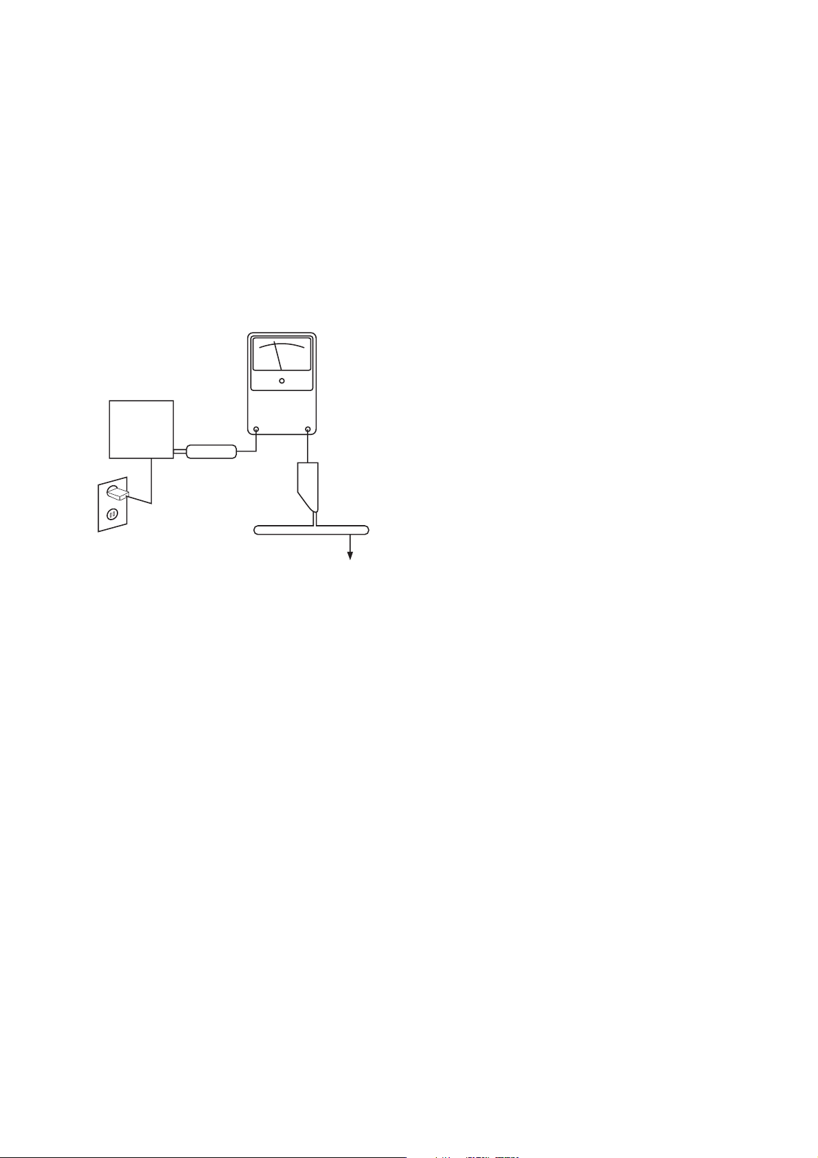
LEAKAGE CURRENT CHECK
Measure leakage current to a known earth ground (water
pipe, conduit, etc.) by connecting a leakage current tester
between the earth ground and all exposed metal parts of the
appliance (input/output terminals, screwheads, metal overlays, control shaft, etc.). Plug the AC line cord of the appliance directly into a 120V AC 60Hz outlet and turn the AC
power switch on. Any current measured must not exceed
0.5mA.
ANY MEASUREMENTS NOT WITHIN THE LIMITS
OUTLINED ABOVE ARE INDICATIVE OF A POTENTIAL SHOCK HAZARD AND MUST BE CORRECTED
BEFORE RETURNING THE APPLIANCE TO THE CUSTOMER.
Reading should
not be above
0.5mA
Earth
ground
Device
under
test
Test all
exposed metal
surfaces
Also test with
plug reversed
(Using AC adapter
plug as required)
Leakage
current
tester
AC Leakage Test
Page 4
- 4 -
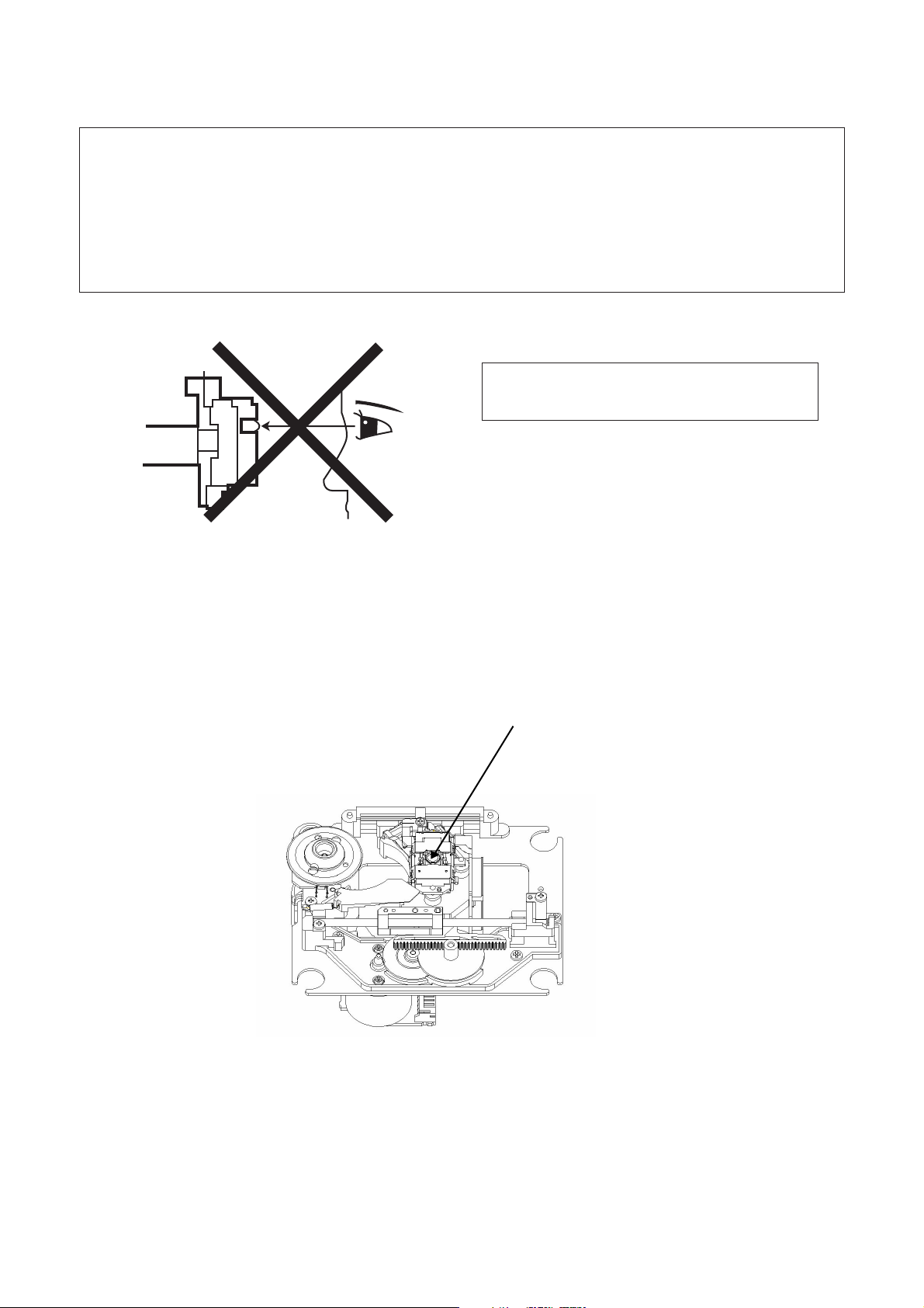
LASER BEAM SAFETY PRECAUTIONS
CLASS 1 LASER PRODUCT
DANGER
INVISIBLE LASER RADIATION
AVOID DIRECT EXPOSURE TO BEAM
This Receiver uses a pickup that emits a laser beam.
The laser beam is emitted from the location shown in the figure. When checking the laser diode, be sure to keep your eyes
at least 1 foot away from the pickup lens when the diode is turned on. Do not look directly at the laser beam.
Caution: Use of controls and adjustments, or doing procedures other than those specified herein, may result in hazardous
radiation exposure.
Do not look directly at the laser beam coming
from the pickup or allow it to strike against your
skin.
Laser Beam Radiation
Page 5
- 5 -
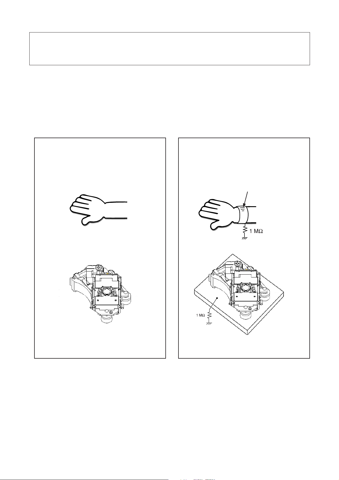
HANDLING LASER PICKUP
The laser diode in the optical system of this receiver can be damaged by electrostatic discharge from clothes,
body, etc. Proper electrostatic grounding for service personnel is required during servicing.
BEFORE REPAIRING THE DVD MECHANISM
a. Human Body Grounding:
Many of the components used in this compact disc player, including the laser pickup, are sensitive to electrostatic discharge.
Service personnel should be grounded with an electrostatic armband (1M ohm).
Caution: Static charge on clothing does not escape through a body grounding wristband. Be careful not to contact the
pickup or electrical components with your clothing.
b. Workbench and Tool Grounding:
A properly-grounded electroconductive plate (1 M ohm) or metal sheet should be fitted to the workbench surface.
Tools and instruments (soldering irons, scopes, etc.) should be grounded to prevent AC leakage.
c. Make two standard ESD solder bridges on the Laser optic PC Board
Before disassembly of mechanism or disconnect any cables in it, make two standard ESD solder bridges on the laser
optic PC Board.
INCORRECT
CORRECT
Ground conductive wristband
for body
Page 6
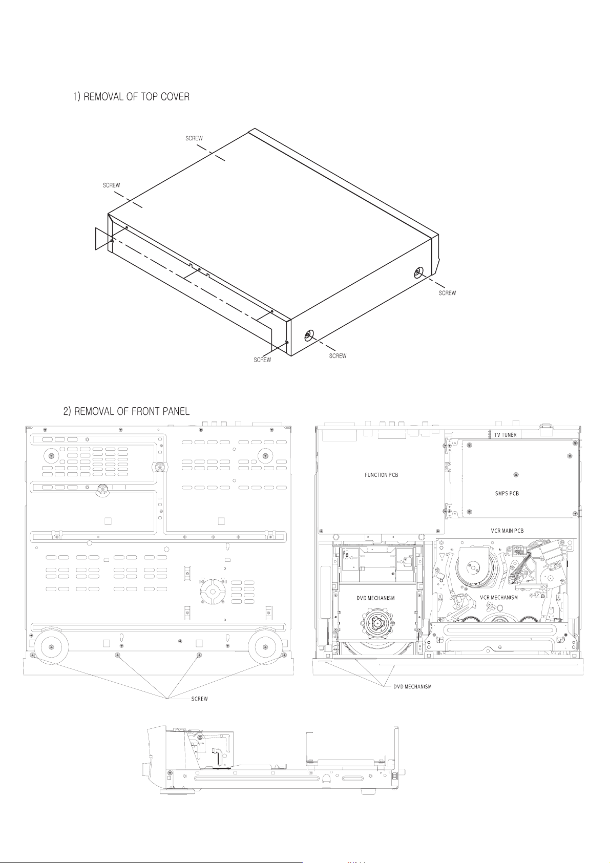
DISASSEMBLY
DISASSEMBLY
-6-
-
Page 7
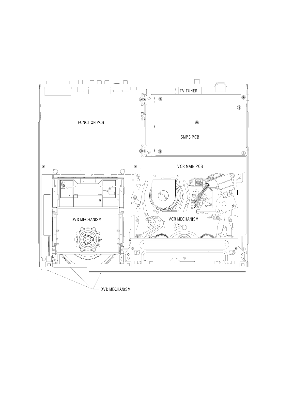
PRINCIPAL PARTS LOCATION
- 7 -
Page 8
TROUBLESHOOTING
Symptom Cause Remedy
No power. The power cord is disconnected. Plug the power cord into the wall outlet securely.
The power is on, but
the DVD player
does not work.
No disc is inserted.
The TV is not set to receive DVD signal
output.
Insert a disc.(Check that the DVD or audio CD indicator
in the DVD display is lit.)
Select the appropiate video input mode on the TV so the
picture from the DVD player appears on the TV screen.
No picture.
The playback
picture is poor.
The DVD/VCR
player does not start
play back.
The remote control
does not work
properly.
The video cable is not connected
securely.
The connected TV power is turned off. Turn on the TV
P-SCAN is selected
The disc is dirty. Clean the disc.
No disc is inserted.
The DVD/VCR player cannot read the
disc because it is damaged or an
incorrect type (for example, a CD-I)
The disc is placed upside down. Place the disc with the playback side down.
The disc is not placed within the guide. Place the disc on the disc tray correctly inside the guide.
The disc is dirty. Clean the disc.
A menu is on the TV screen.
The rating level is set. Cancel the rating function or change the rating level.
The remote control is not pointed at the
remote sensor of the unit.
The remote control is too far from
the unit.
There is an obstacle in the path of the
remote control and the DVD player.
Connect the video cable into jacks securely.
Check the front display. If P-SCAN segment is on, press
"P-SCAN" key of remote control unit.
Insert a disc.(Check that the DVD or CD indicator in the
display is lit.)
Check the a disc type, color system and regional code.
Check for any scratches or smudge on the disc.
Insert a readable disc.
Press SETUP to turn off the manu screen
Point the remote control at the remote sensor of the unit.
Operate the remote control within about 23 feet(7m).
Remove the obstacle.
Recording does
not work properly.
The remote's batteries are exhausted. Replace the batteries with new ones.
Other function is selected. Press the function key what you want to operate. DVD/VCR
The disc is not writable DVD DISC. Remove the disc and insert a proper writable DVD DISC.
The disc is CD-R/RW.
The disc is full. Remove the disc and insert a proper writable DVD DISC.
The disc is dirty. Clean the disc and insert a blank writable DVD DISC.
The disc is a suitable DISC to record. Use the recommended DISC for better operations.
The disc is finalized. Unfinalize the DISC and then record in the DISC.
Only DVD+R/+RW/-R/-RW DISC can be recorded. Remove
the disc and insert a proper writable DVD DISC.
- 8 -
Page 9

Symptom Cause Remedy
d
The disc is not writable DVD DISC. Remove the disc and insert a proper writable DVD DISC.
The disc is CD-R/RW.
Recording does
not work properly.
The DVD/VCR does
not respond when
thebuttons are
pressed.
No sound is output
when a function is
selected.
No image is output
when a function is
selected.
Broadcast stations
cannot be selected
automatically.
The display is dark. The sleep timer is on.
The disc is full. Remove the disc and insert a proper writable DVD DISC.
The disc is dirty. Clean the disc and insert a blank writable DVD DISC.
The disc is a suitable DISC to record. Use the recommended DISC for better operations.
The disc is finalized. Unfinalize the DISC and then record in the DISC.
Static electricity caused by dry air. Disconnect the power plug from the outlet, and insert again.
Improper connections. Make sure the component is connected correctly.
Improper connections. Make sure the component is connected correctly.
The input source is not properly selecte
The siginals are weak. Connect an outdoor antenna.
Only DVD+R/+RW/-R/-RW DISC can be recorded. Remove
the disc and insert a proper writable DVD DISC.
Press the correct function button.
Press SLEEP again
- 9 -
Page 10

TEST MODE
TEST Mode shows the infomation as follows.
I. Back End Version (It is to express each Buyer, each model, and version number.)
II. Front End Version (It is to display the Mecha Fimware version number.)
III. Back End Build time (It can be used to seperate each B/E firmware version by the day.)
IV. Region No.(It is only to display region code.)
[operation]
To enter the first state of test mode, first insert a any DVD DISC and load the DISC.
Then press "STOP" key and the front panel displays "STOP".
then, press key on the remote unit as follows.
[CLEAR] - [2] - [5] - [8] -[0] - [CLEAR]
If you press key correctly, you will see the message below.
Loader FW ver: X.CA05 - (I : F/E version)
Client ver: 0912PT-MODEL NO. - (II : B/E version)
Current Region: < X > - (III : Region Number)
<B/E Firmware update>
The update is done with CD-R. (When the firmware is changed, the updated firmware will be provided by Anam on CD-R)
Put the DISC in TRAY and load the CD-R disc, and Dialogue message to confirm B/E firmware update will be diplayed on the TV screen.
Updating will begin.
You’ll see the update progress
50%
When the TV screen’s display goes off, turn the POWER OFF.
Turn the POWER ON and then DO EEPROM CLEAR.
on the TV screen.
<F/E Firmware update>
The update is done with CD-R. (When the firmware is changed, the updated firmware will be provided by Anam on CD-R)
- Put the disc on TRAY at normal operation mode.
- Load the DISC and Dialogue message to confirm F/E firmware update will be diplayed on the TV screen .
- After about several seconds, DVD door will be open.
- Turn the power off.
- Turn the power on and open DISC
- Remove the disc.
Note: F/E update method has another method. It is that you can update using computer connections.
In this case, you must confirm the F/E firmware version and use a certain provided file
that is able to executive file in computer with EXE extension..
- 10 -
Page 11
RESISTORS AND CAPACITORS
Notes.
* Circuit No's first character indicates kinds of part type.
C : Capacitors
R : Resistors
D : Diode
J : Jumper
L : Coil
Q : Transistors
S : Switch
BK : Bracket
JK : Jack
IC : Integrated Circuit
X : Crystal
BD : Bead
IMPORTANT SAFETY NOTICE
* Components identified by ! Mark have special characteristics important for safety.
* When replacing any of these components, use only manufacture's specified parts.
* The unit of resistance is OHM ( )
K=1000( ), M=1000(K )
* The unit of capacitance is MICROFARAD (uF )
-6
P=10
uF
Numbering System of Resistor
Example
Numbering System of Capacitor
Example
CRD 25 F J 101 HCKR 1H 101 K B
Type Wattage Shape Tolerance Value Type Voltage ValueTolerance Pecularity
Resistor Type Wattage Tolerance Tolerance
K(C/H)RD : Carbon 20 : 1/5W F : 1%
K(C/H)RG : Metal Oxide 25 : 1/4W J : 5% HCB : Ceramic 0J : 6.3V 1H : 50V DC C : 0.25pF
50 : 1/2W K : 10% CCC : Ceramic 1A : 10V 1 : 125V DC G : 2%
1 : 1W CCK : Ceramic 1C: 16V KC : 400V AC J : 5%
K(C/H)RG : Metal Cement 2 : 2W HCQI : Polyester 1E : 25V K : 10%
3 : 3W HCQP : Polypropyene 1H : 50V Z : +80%, -20%
K(H)RJ : Carbon. CHIP 10 : 1/10W HCQS : Polystyrol 1V : 35V
14 : 1/4W HCUS : Ceramic
Capacitor Type
HCEA : ELECT
HCEA : ELECT.CHIP
HCEA Type
Voltage
Other
- 11 -
Page 12

DVD PART
SEQ. PART NO. DESCRIPTION SPECIFICATION REMARKS
CIP11741B FRONT PCB AUTO ASS'Y QRW-6500
CUP11741Z PCB , FRONT QRW-6500
C501 HCBS1H103ZFT CAP , CERAMIC 0.01UF 50V Z
C502 CCEA1CKS470T CAP, ELECT 47UF/16V/5MM HEIGHT 00107-1051
C503 CCEA1CKS101T CAP , ELECT
C504 HCBS1H103ZFT CAP , CERAMIC 0.01UF 50V Z
C505 HCBS1H103ZFT CAP , CERAMIC 0.01UF 50V Z
C506 CCEA1HKS4R7T CAP , ELECT
C507 HCBS1H103ZFT CAP , CERAMIC 0.01UF 50V Z
C508 HCBS1H220JCT CAP , CERAMIC 22PF 50V J
C509 HCBS1H103ZFT CAP , CERAMIC 0.01UF 50V Z
C510 HCBS1H221KBT CAP , CERAMIC 220PF 50V K
C511 HCBS1H220JCT CAP , CERAMIC 22PF 50V J
C512 HCBS1H103ZFT CAP , CERAMIC 0.01UF 50V Z
C513 HCBS1H221KBT CAP , CERAMIC 220PF 50V K
C514 HCBS1H103ZFT CAP , CERAMIC 0.01UF 50V Z
C516 HCBS1H471KBT CAP , CERAMIC
C517 CCEA1CKS100T CAP , ELECT
C519 CCEA1CKS100T CAP , ELECT
C520 HCBS1H471KBT CAP , CERAMIC
C521 HCBS1H220JCT CAP , CERAMIC 22PF 50V J
C523 HCBS1H470KBT CAP , CERAMIC 47PF 50V K
C524 HCBS1H122KBT CAP , CERAMIC
C531 HCBS1H103ZFT CAP , CERAMIC 0.01UF 50V Z
C532 HCBS1H103ZFT CAP , CERAMIC 0.01UF 50V Z
C533 HCBS1H103ZFT CAP , CERAMIC 0.01UF 50V Z
C534 HCBS1H103ZFT CAP , CERAMIC 0.01UF 50V Z
D501 HVD1SS133MT DIODE 1SS133T-77
D502 HVD1SS133MT DIODE 1SS133T-77
D503 HVD1SS133MT DIODE 1SS133T-77
D504 HVD1SS133MT DIODE 1SS133T-77
D505 HVD1SS133MT DIODE 1SS133T-77
D506 HVD1SS133MT DIODE 1SS133T-77
D507 HVD1SS133MT DIODE 1SS133T-77
D508 HVD1SS133MT DIODE 1SS133T-77
D509 HVD1SS133MT DIODE 1SS133T-77
D510 HVD1SS133MT DIODE 1SS133T-77
J501 C3A206 WIRE , COPPER SN95/PB5 , 0.6
J502 C3A206 WIRE , COPPER SN95/PB5 , 0.6
J503 C3A206 WIRE , COPPER SN95/PB5 , 0.6
J504 C3A206 WIRE , COPPER SN95/PB5 , 0.6
J505 C3A206 WIRE , COPPER SN95/PB5 , 0.6
J506 C3A206 WIRE , COPPER SN95/PB5 , 0.6
J507 C3A206 WIRE , COPPER SN95/PB5 , 0.6
J508 C3A206 WIRE , COPPER SN95/PB5 , 0.6
J509 C3A206 WIRE , COPPER SN95/PB5 , 0.6
J512 C3A206 WIRE , COPPER SN95/PB5 , 0.6
J514 C3A206 WIRE , COPPER SN95/PB5 , 0.6
J515 C3A206 WIRE , COPPER SN95/PB5 , 0.6
J516 C3A206 WIRE , COPPER SN95/PB5 , 0.6
J517 C3A206 WIRE , COPPER SN95/PB5 , 0.6
J518 C3A206 WIRE , COPPER SN95/PB5 , 0.6
J519 C3A206 WIRE , COPPER SN95/PB5 , 0.6
J522 C3A206 WIRE , COPPER SN95/PB5 , 0.6
- 12-
Page 13

SEQ. PART NO. DESCRIPTION SPECIFICATION REMARKS
J523 C3A206 WIRE , COPPER SN95/PB5 , 0.6
J526 C3A206 WIRE , COPPER SN95/PB5 , 0.6
L501 HLQ02C100KT COIL , AXAIL
L527 HLQ02C4R7KT COIL , AXIAL 4.7UH K
R501 CRD20TJ272T RES , CARBON 2.7K OHM 1/5W J
R502 CRD20TJ182T RES , CARBON 1.8K OHM 1/5W J
R503 CRD20TJ100T RES , CARBON 10 OHM 1/5W J
R504 CRD20TJ102T RES , CARBON 1K OHM 1/5W J
R506 CRD20TJ102T RES , CARBON 1K OHM 1/5W J
R507 CRD20TJ152T RES , CARBON 1.5K OHM 1/5W J
R508 CRD20TJ562T RES , CARBON 5.6K OHM 1/5W J
R509 CRD20TJ102T RES , CARBON 1K OHM 1/5W J
R510 CRD20TJ152T RES , CARBON 1.5K OHM 1/5W J
R511 CRD20TJ182T RES , CARBON 1.8K OHM 1/5W J
R512 CRD20TJ272T RES , CARBON 2.7K OHM 1/5W J
R513 CRD20TJ332T RES , CARBON 3.3K OHM 1/5W J
R514 CRD20TJ562T RES , CARBON 5.6K OHM 1/5W J
R515 CRD20TJ332T RES , CARBON 3.3K OHM 1/5W J
R516 CRD20TJ562T RES , CARBON 5.6K OHM 1/5W J
R517 CRD20TJ752T RES , CARBON 7.5K OHM 1/5W J
R518 CRD20TJ102T RES , CARBON 1K OHM 1/5W J
R519 CRD20TJ473T RES , CARBON 47K OHM 1/5W J
R520 CRD20TJ101T RES , CARBON 100 OHM 1/5W J
R521 CRD20TJ473T RES , CARBON 47K OHM 1/5W J
R522 CRD20TJ101T RES , CARBON 100 OHM 1/5W J
R524 CRD20TJ820T RES , CARBON 82 OHM 1/5W J
R526 CRD20TJ123T RES , CARBON 12K OHM 1/5W J
R527 CRD20TJ153T RES , CARBON 15K OHM 1/5W J
SW01 CST1A012ZT SW , TACT 00802-0005
SW02 CST1A012ZT SW , TACT 00802-0005
SW03 CST1A012ZT SW , TACT 00802-0005
SW04 CST1A012ZT SW , TACT 00802-0005
SW05 CST1A012ZT SW , TACT 00802-0005
SW06 CST1A012ZT SW , TACT 00802-0005
SW07 CST1A012ZT SW , TACT 00802-0005
SW08 CST1A012ZT SW , TACT 00802-0005
SW09 CST1A012ZT SW , TACT 00802-0005
SW10 CST1A012ZT SW , TACT 00802-0005
SW11 CST1A012ZT SW , TACT 00802-0005
SW12 CST1A012ZT SW , TACT 00802-0005
SW13 CST1A012ZT SW , TACT 00802-0005
SW14 CST1A012ZT SW , TACT 00802-0005
SW15 CST1A012ZT SW , TACT 00802-0005
SW16 CST1A012ZT SW , TACT 00802-0005
SW17 CST1A012ZT SW , TACT 00802-0005
C8ESM800 FLUX
H2K31161 SOLDER , WIRE SN60/PH40
H2K50301 SOLDER , BAR S63S-W3.0
K4FM073 TAPE , BOTH SIDE 3M #4920
BK51 CMC1A242 PLATE , EARTH QRW-6500
BK52 CMC1A242 PLATE , EARTH QRW-6500
BK53 CMD1A468 BRACKET , FLT
BK54 CMD1A468 BRACKET , FLT
BN51 CWB1B903150NE WIRE ASS'Y
- 13-
Page 14

SEQ. PART NO. DESCRIPTION SPECIFICATION REMARKS
BN53 CWBQRW6500BN53 WIRE ASS'Y (11 PIN) QRW-6500
BN79 CWE7202050AR WIRE A'SSY
CB71 CWC1B4A19A400B CARD CABLE
CN52 CJP03GA19ZY WAFER, STRAIGHT, 3PIN
CN71 KJP19GA117ZG WAFER , C.CABLE
FIP1 HFL11BT229GNK FIP
IC51 HRVKSM603TH2 REMOCON SENSER CN KSM-603TH2
IC52 HVILC75725E IC , VFL DRIVER
IC93 HVINJM2068MDTE1 I.C , OP AMP NJM2068MD-TE1
JK51 CJJ9M004Z JACK , S-VHS
JK52 CJJ4S028Z JACK , BOARD (3P) ADVR-7100
- 14-
Page 15

SEQ. PART NO. DESCRIPTION SPECIFICATION REMARKS
CIP11742B FUNCTION PCB AUTO ASS'Y
CIP11742BSMD FUNCTION PCB SMD ASS'Y
CUP11742Z PCB , FUNCTION
C101 HCUS1H680JA CAP , CHIP
C104 HCUS1H103KC CAP , CHIP
C105 HCUS1H680JA CAP , CHIP
C106 HCUS1H680JA CAP , CHIP
C107 HCUS1H101JA CAP , CHIP
C108 HCUS1H101JA CAP , CHIP
C109 HCUS1H101JA CAP , CHIP
C110 HCUS1H470JA CAP , CHIP
C111 HCUS1H103KC CAP , CHIP
C113 HCUS1H470JA CAP , CHIP
C114 HCUS1H221JA CAP , CHIP
C115 HCUS1H103KC CAP , CHIP
C120 HCUS1H221JA CAP , CHIP
C121 HCUS1H150JA CAP , CHIP 1608 SIZE
C122 HCUS1H150JA CAP , CHIP 1608 SIZE
C123 HCUS1H101JA CAP , CHIP
C124 HCUS1H101JA CAP , CHIP
C125 HCUS1H220JA CAP , CHIP
C126 HCUS1H220JA CAP , CHIP
C127 HCUS1H220JA CAP , CHIP
C128 HCUS1H680JA CAP , CHIP
C129 HCUS1H151JA CAP , CHIP , 150PF JA 1608 SIZE
C131 HCUS1H221JA CAP , CHIP
C132 HCUS1H221JA CAP , CHIP
C133 HCUS1H101JA CAP , CHIP
C134 CCEA1CH101T CAP, ELE 100UF/16V/-40~+85 00107-1003
C135 CCEA1CH101T CAP, ELE 100UF/16V/-40~+85 00107-1003
C136 HCUS1H103KC CAP , CHIP
C151 HCUS1E104ZF CAP , CHIP , 0.1UF ZF 1608 SIZE
C155 HCUS1H103KC CAP , CHIP
C156 HCUS1H103KC CAP , CHIP
C161 HCUS1H103KC CAP , CHIP
C201 HCUS1H150JA CAP , CHIP 1608 SIZE
C202 HCUS1H151JA CAP , CHIP , 150PF JA 1608 SIZE
C203 HCUS1H151JA CAP , CHIP , 150PF JA 1608 SIZE
C206 HCUS1H150JA CAP , CHIP 1608 SIZE
C207 HCUS1H151JA CAP , CHIP , 150PF JA 1608 SIZE
C208 HCUS1H151JA CAP , CHIP , 150PF JA 1608 SIZE
C211 HCUS1H150JA CAP , CHIP 1608 SIZE
C212 HCUS1H151JA CAP , CHIP , 150PF JA 1608 SIZE
C213 HCUS1H151JA CAP , CHIP , 150PF JA 1608 SIZE
C216 HCUS1H150JA CAP , CHIP 1608 SIZE
C217 HCUS1H151JA CAP , CHIP , 150PF JA 1608 SIZE
C218 HCUS1H151JA CAP , CHIP , 150PF JA 1608 SIZE
C221 HCUS1H150JA CAP , CHIP 1608 SIZE
C222 HCUS1H151JA CAP , CHIP , 150PF JA 1608 SIZE
C223 HCUS1H151JA CAP , CHIP , 150PF JA 1608 SIZE
C226 HCUS1H150JA CAP , CHIP 1608 SIZE
C227 HCUS1H151JA CAP , CHIP , 150PF JA 1608 SIZE
C228 HCUS1H151JA CAP , CHIP , 150PF JA 1608 SIZE
C231 HCUS1H221JA CAP , CHIP
QRW-6500
QRW-6500
QRW-6500
- 15-
Page 16

SEQ. PART NO. DESCRIPTION SPECIFICATION REMARKS
C236 HCUS1H221JA CAP , CHIP
C242 HCUS1E104ZF CAP , CHIP , 0.1UF ZF 1608 SIZE
C246 HCUS1H104ZF CAP , CHIP
C248 HCUS1H104ZF CAP , CHIP
C251 HCUS1H270JA CAP , CHIP , 27PF JA 1608 SIZE
C252 HCUS1H270JA CAP , CHIP , 27PF JA 1608 SIZE
C253 HCUS1H270JA CAP , CHIP , 27PF JA 1608 SIZE
C254 HCUS1H270JA CAP , CHIP , 27PF JA 1608 SIZE
C255 HCUS1H270JA CAP , CHIP , 27PF JA 1608 SIZE
C256 HCUS1H270JA CAP , CHIP , 27PF JA 1608 SIZE
C257 HCUS1H270JA CAP , CHIP , 27PF JA 1608 SIZE
C261 HCUS1H220JA CAP , CHIP
C263 HCUS1H220JA CAP , CHIP
C265 HCUS1H220JA CAP , CHIP
C267 HCUS1H220JA CAP , CHIP
C269 HCUS1H220JA CAP , CHIP
C273 HCUS1H224ZF CAP , CHIP
C275 HCUS1H104ZF CAP , CHIP
C276 HCUS1E104ZF CAP , CHIP , 0.1UF ZF 1608 SIZE
C279 HCUS1H103KC CAP , CHIP
C281 CRJ10DJ223T RES, CHIP 22KOHM/1608/5% 00200-0093
C282 CRJ10DJ223T RES, CHIP 22KOHM/1608/5% 00200-0093
C283 CRJ10DJ223T RES, CHIP 22KOHM/1608/5% 00200-0093
C284 HCUS1H103KC CAP , CHIP
C286 HCUS1H103KC CAP , CHIP
C297 HCUS1H103KC CAP , CHIP
C317 HCUS1H471JA CAP , CHIP
C318 HCUS1H471JA CAP , CHIP
C319 HCUS1H103KC CAP , CHIP
C320 HCUS1H103KC CAP , CHIP
C326 HCUS1H103KC CAP , CHIP
C327 HCUS1H103KC CAP , CHIP
C329 HCUS1H103KC CAP , CHIP
C336 HCUS1H103KC CAP , CHIP
C337 HCUS1H103KC CAP , CHIP
C339 HCUS1H103KC CAP , CHIP
C346 HCUS1H103KC CAP , CHIP
C347 HCUS1H103KC CAP , CHIP
C365 HCUS1H220JA CAP , CHIP
C367 HCUS1H220JA CAP , CHIP
C371 HCUS1E104ZF CAP , CHIP , 0.1UF ZF 1608 SIZE
C373 HCUS1H220JA CAP , CHIP
C375 HCUS1H220JA CAP , CHIP
C376 HCUS1E104ZF CAP , CHIP , 0.1UF ZF 1608 SIZE
C377 HCUS1H330JA CAP , CHIP
C381 HCUS1H100JA CAP , CHIP
C508 HCUS1H101JA CAP , CHIP
C509 HCUS1H101JA CAP , CHIP
C518 HCUS1H101JA CAP , CHIP
C519 HCUS1H101JA CAP , CHIP
C528 HCUS1H102KC CAP , CHIP
C529 HCUS1H103KC CAP , CHIP
C530 HCUS1H101JA CAP , CHIP
C531 HCUS1H101JA CAP , CHIP
- 16-
Page 17

SEQ. PART NO. DESCRIPTION SPECIFICATION REMARKS
C535 HCUS1H101JA CAP , CHIP
C545 HCUS1H101JA CAP , CHIP
C546 HCUS1H101JA CAP , CHIP
C561 HCUS1H101JA CAP , CHIP
C562 HCUS1H101JA CAP , CHIP
C576 HCUS1H101JA CAP , CHIP
C577 HCUS1H101JA CAP , CHIP
C591 HCUS1H101JA CAP , CHIP
C592 HCUS1H101JA CAP , CHIP
C601 HCUS1H101JA CAP , CHIP
C602 HCUS1H101JA CAP , CHIP
C603 HCUS1H101JA CAP , CHIP
C604 HCUS1H101JA CAP , CHIP
C609 HCUS1H101JA CAP , CHIP
C610 HCUS1H101JA CAP , CHIP
C620 HCUS1H103KC CAP , CHIP
C621 HCUS1H103KC CAP , CHIP
C624 HCUS1H101JA CAP , CHIP
C625 HCUS1H101JA CAP , CHIP
C628 HCUS1H101JA CAP , CHIP
C629 HCUS1H101JA CAP , CHIP
C631 HCUS1H151JA CAP , CHIP , 150PF JA 1608 SIZE
C632 HCUS1H151JA CAP , CHIP , 150PF JA 1608 SIZE
C633 HCUS1H103KC CAP , CHIP
C634 HCUS1H103KC CAP , CHIP
C635 HCUS1H101JA CAP , CHIP
C636 HCUS1H101JA CAP , CHIP
C637 HCUS1H101JA CAP , CHIP
C638 HCUS1H101JA CAP , CHIP
C646 HCUS1H151JA CAP , CHIP , 150PF JA 1608 SIZE
C647 HCUS1H151JA CAP , CHIP , 150PF JA 1608 SIZE
C648 HCUS1H103KC CAP , CHIP
C650 HCUS1H103KC CAP , CHIP
C652 HCUS1H101JA CAP , CHIP
C653 HCUS1H101JA CAP , CHIP
C656 HCUS1H101JA CAP , CHIP
C657 HCUS1H101JA CAP , CHIP
C661 HCUS1H470JA CAP , CHIP
C662 HCUS1H470JA CAP , CHIP
C663 HCUS1H103KC CAP , CHIP
C664 HCUS1H103KC CAP , CHIP
C665 HCUS1H470JA CAP , CHIP
C666 HCUS1H470JA CAP , CHIP
C671 HCUS1H470JA CAP , CHIP
C672 HCUS1H470JA CAP , CHIP
C673 HCUS1H103KC CAP , CHIP
C674 HCUS1H103KC CAP , CHIP
C675 HCUS1H470JA CAP , CHIP
C676 HCUS1H470JA CAP , CHIP
C677 HCUS1H470JA CAP , CHIP
C678 HCUS1H470JA CAP , CHIP
C682 CRJ10DJ0R0T RES, CHIP 0 OHM/1608/5% 00200-0090
C691 HCUS1E104ZF CAP , CHIP , 0.1UF ZF 1608 SIZE
C692 HCUS1E104ZF CAP , CHIP , 0.1UF ZF 1608 SIZE
- 17-
Page 18

SEQ. PART NO. DESCRIPTION SPECIFICATION REMARKS
C701 HCUS1H103KC CAP , CHIP
C702 HCUS1H103KC CAP , CHIP
C703 HCUS1H271JA CAP , CHIP
C704 HCUS1H271JA CAP , CHIP
C707 HCUS1H271JA CAP , CHIP
C708 HCUS1H271JA CAP , CHIP
C711 HCUS1H103KC CAP , CHIP
C712 HCUS1H103KC CAP , CHIP
C713 HCUS1H271JA CAP , CHIP
C714 HCUS1H271JA CAP , CHIP
C717 HCUS1H271JA CAP , CHIP
C718 HCUS1H271JA CAP , CHIP
C721 HCUS1H271JA CAP , CHIP
C722 HCUS1H271JA CAP , CHIP
C728 HCUS1H103KC CAP , CHIP
C729 HCUS1H103KC CAP , CHIP
C731 HCUS1H271JA CAP , CHIP
C732 HCUS1H271JA CAP , CHIP
C733 HCUS1H271JA CAP , CHIP
C734 HCUS1H271JA CAP , CHIP
C743 HCUS1H103KC CAP , CHIP
C744 HCUS1H103KC CAP , CHIP
C751 HCUS1H470JA CAP , CHIP
C752 HCUS1H470JA CAP , CHIP
C753 HCUS1H103KC CAP , CHIP
C754 HCUS1H103KC CAP , CHIP
C759 HCUS1H271JA CAP , CHIP
C760 HCUS1H271JA CAP , CHIP
C801 HCUS1H103KC CAP , CHIP
C802 HCUS1H103KC CAP , CHIP
C807 HCUS1H103KC CAP , CHIP
C808 HCUS1H103KC CAP , CHIP
C821 HCUS1H103KC CAP , CHIP
C822 HCUS1H103KC CAP , CHIP
C851 HCUS1H101JA CAP , CHIP
C852 HCUS1H101JA CAP , CHIP
C860 HCUS1H101JA CAP , CHIP
C864 HCUS1H101JA CAP , CHIP
C875 HCUS1H101JA CAP , CHIP
C883 HCUS1H221JA CAP , CHIP
C884 HCUS1H221JA CAP , CHIP
C885 HCUS1H271JA CAP , CHIP
C886 HCUS1H271JA CAP , CHIP
C944 HCUS1H221JA CAP , CHIP
C945 HCUS1H271JA CAP , CHIP
C946 HCUS1H221JA CAP , CHIP
C947 HCUS1H271JA CAP , CHIP
C948 HCUS1H221JA CAP , CHIP
C949 HCUS1H271JA CAP , CHIP
C961 HCUS1H271JA CAP , CHIP
C962 HCUS1H271JA CAP , CHIP
C963 HCUS1H103KC CAP , CHIP
C964 HCUS1H103KC CAP , CHIP
C967 HCUS1H271JA CAP , CHIP
- 18-
Page 19

SEQ. PART NO. DESCRIPTION SPECIFICATION REMARKS
C968 HCUS1H271JA CAP , CHIP
C971 HCUS1H103KC CAP , CHIP
C972 HCUS1H103KC CAP , CHIP
C975 HCUS1H271JA CAP , CHIP
C976 HCUS1H271JA CAP , CHIP
C987 HCUS1H220JA CAP , CHIP
C988 HCUS1H220JA CAP , CHIP
D136 HVD1SS355T DIODE , CHIP
D137 HVD1SS355T DIODE , CHIP
D295 HVD1SS355T DIODE , CHIP
FB24 HLZ9Z008Z CHIP , BEAD
FB27 HLZ9Z008Z CHIP , BEAD
FB37 HLZ9Z008Z CHIP , BEAD
IC10 HVIRH5VT28C I.C , RESET RICOH 2.8V
IC11 HVIRH5VT45C I.C , RESET RICOH 4.5V
IC14 HVIST92F124V1T6 I.C , MCU (FLASH 128K,TQFP100) ST92F124V1T6
IC24 HVIAK5381VT I.C , ADC
IC27 KVIBA7607F I.C , VIDEO SIGNAL SWITCHER BA7607F
IC29 HVIPCM1754DBQR I.C , 2CH DAC PCM1754DBQR
IC31 HVINJM2068MDTE1 I.C , OP AMP NJM2068MD-TE1
IC34 HVINJM2580MTE1 I.C , TRIPLE VIDEO AMPLIFIER QRW-7500
IC35 HVINJM2580MTE1 I.C , TRIPLE VIDEO AMPLIFIER QRW-7500
IC37 HVI74VHC04MX I.C , INVERTER 74VHC04M
IC62 HVINJM2068MDTE1 I.C , OP AMP NJM2068MD-TE1
IC63 HVINJM2068MDTE1 I.C , OP AMP NJM2068MD-TE1
IC64 HVINJM2068MDTE1 I.C , OP AMP NJM2068MD-TE1
IC66 HVINJM2068MDTE1 I.C , OP AMP NJM2068MD-TE1
IC67 HVINJM2068MDTE1 I.C , OP AMP NJM2068MD-TE1
IC68 HVITC9164AF I.C , FUNCTION TC9164AF
IC70 HVINJM2068MDTE1 I.C , OP AMP NJM2068MD-TE1
IC71 HVINJM2068MDTE1 I.C , OP AMP NJM2068MD-TE1
IC72 HVITC9163AF I.C , FUNCTION TC9163AF
IC73 HVINJM2068MDTE1 I.C , OP AMP NJM2068MD-TE1
IC74 HVITC9162AF I.C , FUNCTION TC9162AF
IC75 HVINJM2068MDTE1 I.C , OP AMP NJM2068MD-TE1
IC76 HVINJM2068MDTE1 I.C , OP AMP NJM2068MD-TE1
IC79 HVINJM2296M I.C , VIDEO SW NJM2296M
IC80 HVINJM2296M I.C , VIDEO SW NJM2296M
IC81 HVINJM2244MTE1 I.C , VIDEO SWITCH QRW-6500
IC82 HVINJM2244MTE1 I.C , VIDEO SWITCH QRW-6500
IC96 HVINJM2068MDTE1 I.C , OP AMP NJM2068MD-TE1
IC97 HVINJM2068MDTE1 I.C , OP AMP NJM2068MD-TE1
L201 HLQ09E1R0KRZ CHIP , COIL FI-C3216-102
L206 HLQ09E1R0KRZ CHIP , COIL FI-C3216-102
L211 HLQ09E1R0KRZ CHIP , COIL FI-C3216-102
L216 HLQ09E1R0KRZ CHIP , COIL FI-C3216-102
L221 HLQ09E1R0KRZ CHIP , COIL FI-C3216-102
L226 HLQ09E1R0KRZ CHIP , COIL FI-C3216-102
L282 CRJ10DJ0R0T RES, CHIP 0 OHM/1608/5% 00200-0090
L283 CRJ10DJ0R0T RES, CHIP 0 OHM/1608/5% 00200-0090
L860 HLQ09E1R0KRZ CHIP , COIL FI-C3216-102
L881 HLQ09E1R0KRZ CHIP , COIL FI-C3216-102
L882 HLQ09E1R0KRZ CHIP , COIL FI-C3216-102
L945 HLQ09E1R0KRZ CHIP , COIL FI-C3216-102
- 19-
Page 20

SEQ. PART NO. DESCRIPTION SPECIFICATION REMARKS
L947 HLQ09E1R0KRZ CHIP , COIL FI-C3216-102
L949 HLQ09E1R0KRZ CHIP , COIL FI-C3216-102
Q101 HVTKRA102S T.R , CHIP KRA102S
Q102 HVTKRA102S T.R , CHIP KRA102S
Q103 HVTKRA102S T.R , CHIP KRA102S
Q105 HVTKRC102S T.R , CHIP KRC102S
Q106 HVTKRC102S T.R , CHIP KRC102S
Q141 HVTKRA102S T.R , CHIP KRA102S
Q142 HVTKRA102S T.R , CHIP KRA102S
Q143 HVTKRA102S T.R , CHIP KRA102S
Q144 HVTKRA102S T.R , CHIP KRA102S
Q145 HVTKRA102S T.R , CHIP KRA102S
Q146 HVTKRA102S T.R , CHIP KRA102S
Q161 HVTKRA102S T.R , CHIP KRA102S
Q162 HVTKRC102S T.R , CHIP KRC102S
Q163 HVTKRC102S T.R , CHIP KRC102S
Q303 HVTKTD1304T T.R , CHIP (MUTE) KTD1304
Q304 HVTKTD1304T T.R , CHIP (MUTE) KTD1304
Q310 HVTKRC102S T.R , CHIP KRC102S
Q311 HVTKRA102S T.R , CHIP KRA102S
Q364 HVTKTD1304T T.R , CHIP (MUTE) KTD1304
Q366 HVTKTD1304T T.R , CHIP (MUTE) KTD1304
Q504 HVTKTA1504SYRTK T.R , CHIP KTA1504S Y RTK
Q505 HVTKTA1504SYRTK T.R , CHIP KTA1504S Y RTK
Q516 HVTKTA1504SYRTK T.R , CHIP KTA1504S Y RTK
Q517 HVTKTA1504SYRTK T.R , CHIP KTA1504S Y RTK
Q524 HVTKTA1504SYRTK T.R , CHIP KTA1504S Y RTK
Q525 HVTKTA1504SYRTK T.R , CHIP KTA1504S Y RTK
Q539 HVTKTA1504SYRTK T.R , CHIP KTA1504S Y RTK
Q540 HVTKTA1504SYRTK T.R , CHIP KTA1504S Y RTK
Q555 HVTKTA1504SYRTK T.R , CHIP KTA1504S Y RTK
Q556 HVTKTA1504SYRTK T.R , CHIP KTA1504S Y RTK
Q560 HVTKRC102S T.R , CHIP KRC102S
Q561 HVTKRA102S T.R , CHIP KRA102S
Q569 HVTKTA1504SYRTK T.R , CHIP KTA1504S Y RTK
Q570 HVTKTA1504SYRTK T.R , CHIP KTA1504S Y RTK
Q585 HVTKTA1504SYRTK T.R , CHIP KTA1504S Y RTK
Q586 HVTKTA1504SYRTK T.R , CHIP KTA1504S Y RTK
Q845 HVTKTA1504SYRTK T.R , CHIP KTA1504S Y RTK
Q846 HVTKTA1504SYRTK T.R , CHIP KTA1504S Y RTK
Q857 HVTKTA1504SYRTK T.R , CHIP KTA1504S Y RTK
Q862 HVTKTA1504SYRTK T.R , CHIP KTA1504S Y RTK
Q873 HVTKTA1504SYRTK T.R , CHIP KTA1504S Y RTK
Q881 HVTKTA1504SYRTK T.R , CHIP KTA1504S Y RTK
Q882 HVTKTA1504SYRTK T.R , CHIP KTA1504S Y RTK
Q951 HVTKRC102S T.R , CHIP KRC102S
Q982 HVTKTD1304T T.R , CHIP (MUTE) KTD1304
Q983 HVTKTD1304T T.R , CHIP (MUTE) KTD1304
R101 CRJ10DJ750T RES , CHIP 1608 SIZE
R102 CRJ10DJ100T RES , CHIP 1608 SIZE
R103 CRJ10DJ100T RES , CHIP 1608 SIZE
R104 CRJ10DJ221T RES, CHIP 220 OHM/1608/5% 00200-0101
R105 CRJ10DJ102T RES, CHIP 1KOHM/1608/5% 00200-0094
R106 CRJ10DJ102T RES, CHIP 1KOHM/1608/5% 00200-0094
-20-
Page 21

SEQ. PART NO. DESCRIPTION SPECIFICATION REMARKS
R107 CRJ10DJ102T RES, CHIP 1KOHM/1608/5% 00200-0094
R108 CRJ10DJ750T RES , CHIP 1608 SIZE
R109 CRJ10DJ0R0T RES, CHIP 0 OHM/1608/5% 00200-0090
R110 CRJ10DJ331T RES, CHIP 330 OHM/1608/5% 00200-0117
R111 CRJ10DJ100T RES , CHIP 1608 SIZE
R112 CRJ10DJ223T RES, CHIP 22KOHM/1608/5% 00200-0093
R113 CRJ10DJ331T RES, CHIP 330 OHM/1608/5% 00200-0117
R114 CRJ10DJ0R0T RES, CHIP 0 OHM/1608/5% 00200-0090
R115 CRJ10DJ100T RES , CHIP 1608 SIZE
R116 CRJ10DJ223T RES, CHIP 22KOHM/1608/5% 00200-0093
R117 CRJ10DJ100T RES , CHIP 1608 SIZE
R118 CRJ10DJ750T RES , CHIP 1608 SIZE
R119 CRJ10DJ822T RES , CHIP 1608 SIZE
R120 CRJ10DJ822T RES , CHIP 1608 SIZE
R121 CRJ10DJ121T RES , CHIP 1608 SIZE
R122 CRJ10DJ0R0T RES, CHIP 0 OHM/1608/5% 00200-0090
R124 CRJ10DJ0R0T RES, CHIP 0 OHM/1608/5% 00200-0090
R125 CRJ10DJ0R0T RES, CHIP 0 OHM/1608/5% 00200-0090
R126 CRJ10DJ0R0T RES, CHIP 0 OHM/1608/5% 00200-0090
R127 CRJ10DJ103T RES, CHIP 10KOHM/1608/5% 00200-0096
R128 CRJ10DJ103T RES, CHIP 10KOHM/1608/5% 00200-0096
R129 CRJ10DJ103T RES, CHIP 10KOHM/1608/5% 00200-0096
R130 CRJ10DJ0R0T RES, CHIP 0 OHM/1608/5% 00200-0090
R131 CRJ10DJ100T RES , CHIP 1608 SIZE
R132 CRJ10DJ100T RES , CHIP 1608 SIZE
R133 CRJ10DJ100T RES , CHIP 1608 SIZE
R134 CRJ10DJ100T RES , CHIP 1608 SIZE
R135 CRJ10DJ100T RES , CHIP 1608 SIZE
R136 CRJ10DJ100T RES , CHIP 1608 SIZE
R137 CRJ10DJ100T RES , CHIP 1608 SIZE
R138 CRJ10DJ0R0T RES, CHIP 0 OHM/1608/5% 00200-0090
R139 CRJ10DJ331T RES, CHIP 330 OHM/1608/5% 00200-0117
R140 CRJ10DJ331T RES, CHIP 330 OHM/1608/5% 00200-0117
R141 CRJ10DJ102T RES, CHIP 1KOHM/1608/5% 00200-0094
R142 CRJ10DJ102T RES, CHIP 1KOHM/1608/5% 00200-0094
R143 CRJ10DJ102T RES, CHIP 1KOHM/1608/5% 00200-0094
R144 CRJ10DJ102T RES, CHIP 1KOHM/1608/5% 00200-0094
R145 CRJ10DJ102T RES, CHIP 1KOHM/1608/5% 00200-0094
R146 CRJ10DJ102T RES, CHIP 1KOHM/1608/5% 00200-0094
R147 CRJ10DJ0R0T RES, CHIP 0 OHM/1608/5% 00200-0090
R148 CRJ10DJ101T RES, CHIP 100 OHM/1608/5% 00200-0100
R149 CRJ10DJ101T RES, CHIP 100 OHM/1608/5% 00200-0100
R155 CRJ10DJ101T RES, CHIP 100 OHM/1608/5% 00200-0100
R156 CRJ10DJ101T RES, CHIP 100 OHM/1608/5% 00200-0100
R161 CRJ10DJ223T RES, CHIP 22KOHM/1608/5% 00200-0093
R162 CRJ10DJ101T RES, CHIP 100 OHM/1608/5% 00200-0100
R163 CRJ10DJ103T RES, CHIP 10KOHM/1608/5% 00200-0096
R164 CRJ10DJ103T RES, CHIP 10KOHM/1608/5% 00200-0096
R166 CRJ10DJ100T RES , CHIP 1608 SIZE
R167 CRJ10DJ222T RES, CHIP 2.2KOHM/1608/5% 00200-0142
R168 CRJ10DJ392T RES . CHIP
R201 CRJ10DF75R0T RES, CHIP 75 OHM/1608/1% 75 OHM, 1%
R206 CRJ10DF75R0T RES, CHIP 75 OHM/1608/1% 75 OHM, 1%
R211 CRJ10DF75R0T RES, CHIP 75 OHM/1608/1% 75 OHM, 1%
-21 -
Page 22

SEQ. PART NO. DESCRIPTION SPECIFICATION REMARKS
R216 CRJ10DF75R0T RES, CHIP 75 OHM/1608/1% 75 OHM, 1%
R221 CRJ10DF75R0T RES, CHIP 75 OHM/1608/1% 75 OHM, 1%
R226 CRJ10DF75R0T RES, CHIP 75 OHM/1608/1% 75 OHM, 1%
R231 CRJ10DJ0R0T RES, CHIP 0 OHM/1608/5% 00200-0090
R232 CRJ10DJ104T RES, CHIP 100KOHM/1608/5% 00200-0097
R236 CRJ10DJ0R0T RES, CHIP 0 OHM/1608/5% 00200-0090
R237 CRJ10DJ104T RES, CHIP 100KOHM/1608/5% 00200-0097
R241 CRJ10DJ221T RES, CHIP 220 OHM/1608/5% 00200-0101
R242 CRJ10DJ100T RES , CHIP 1608 SIZE
R243 CRJ10DJ100T RES , CHIP 1608 SIZE
R254 CRJ10DJ103T RES, CHIP 10KOHM/1608/5% 00200-0096
R255 CRJ10DJ100T RES , CHIP 1608 SIZE
R256 CRJ10DJ0R0T RES, CHIP 0 OHM/1608/5% 00200-0090
R257 CRJ10DJ0R0T RES, CHIP 0 OHM/1608/5% 00200-0090
R258 CRJ10DJ0R0T RES, CHIP 0 OHM/1608/5% 00200-0090
R261 CRJ10DJ470T RES, CHIP 47 OHM/1608/5% 00200-0098
R263 CRJ10DJ470T RES, CHIP 47 OHM/1608/5% 00200-0098
R265 CRJ10DJ470T RES, CHIP 47 OHM/1608/5% 00200-0098
R267 CRJ10DJ470T RES, CHIP 47 OHM/1608/5% 00200-0098
R269 CRJ10DJ470T RES, CHIP 47 OHM/1608/5% 00200-0098
R271 CRJ10DJ0R0T RES, CHIP 0 OHM/1608/5% 00200-0090
R272 CRJ10DJ103T RES, CHIP 10KOHM/1608/5% 00200-0096
R273 CRJ10DJ0R0T RES, CHIP 0 OHM/1608/5% 00200-0090
R274 CRJ10DJ103T RES, CHIP 10KOHM/1608/5% 00200-0096
R275 CRJ10DJ0R0T RES, CHIP 0 OHM/1608/5% 00200-0090
R276 CRJ10DJ103T RES, CHIP 10KOHM/1608/5% 00200-0096
R277 CRJ10DJ0R0T RES, CHIP 0 OHM/1608/5% 00200-0090
R284 CRJ10DJ103T RES, CHIP 10KOHM/1608/5% 00200-0096
R289 CRJ10DJ103T RES, CHIP 10KOHM/1608/5% 00200-0096
R291 CRJ10DJ101T RES, CHIP 100 OHM/1608/5% 00200-0100
R292 CRJ10DJ101T RES, CHIP 100 OHM/1608/5% 00200-0100
R293 CRJ10DJ101T RES, CHIP 100 OHM/1608/5% 00200-0100
R294 CRJ10DJ101T RES, CHIP 100 OHM/1608/5% 00200-0100
R295 CRJ10DJ0R0T RES, CHIP 0 OHM/1608/5% 00200-0090
R296 CRJ10DJ0R0T RES, CHIP 0 OHM/1608/5% 00200-0090
R297 CRJ10DJ102T RES, CHIP 1KOHM/1608/5% 00200-0094
R301 CRJ10DJ102T RES, CHIP 1KOHM/1608/5% 00200-0094
R302 CRJ10DJ102T RES, CHIP 1KOHM/1608/5% 00200-0094
R303 CRJ10DJ152T RES, CHIP 1.5KOHM/1608/5% 00200-0119
R304 CRJ10DJ152T RES, CHIP 1.5KOHM/1608/5% 00200-0119
R305 CRJ10DJ103T RES, CHIP 10KOHM/1608/5% 00200-0096
R306 CRJ10DJ103T RES, CHIP 10KOHM/1608/5% 00200-0096
R307 CRJ10DJ392T RES . CHIP
R308 CRJ10DJ392T RES . CHIP
R309 CRJ10DJ392T RES . CHIP
R310 CRJ10DJ392T RES . CHIP
R311 CRJ10DJ103T RES, CHIP 10KOHM/1608/5% 00200-0096
R312 CRJ10DJ103T RES, CHIP 10KOHM/1608/5% 00200-0096
R313 CRJ10DJ223T RES, CHIP 22KOHM/1608/5% 00200-0093
R314 CRJ10DJ223T RES, CHIP 22KOHM/1608/5% 00200-0093
R315 CRJ10DJ102T RES, CHIP 1KOHM/1608/5% 00200-0094
R316 CRJ10DJ102T RES, CHIP 1KOHM/1608/5% 00200-0094
R317 CRJ10DJ104T RES, CHIP 100KOHM/1608/5% 00200-0097
R318 CRJ10DJ104T RES, CHIP 100KOHM/1608/5% 00200-0097
-22-
Page 23
SEQ. PART NO. DESCRIPTION SPECIFICATION REMARKS
R319 CRJ10DJ101T RES, CHIP 100 OHM/1608/5% 00200-0100
R320 CRJ10DJ101T RES, CHIP 100 OHM/1608/5% 00200-0100
R322 CRJ10DJ910T RES , CHIP 1608 SIZE
R323 CRJ10DJ181T RES, CHIP 180 OHM/1608/5% 00200-0203
R324 CRJ10DJ750T RES , CHIP 1608 SIZE
R325 CRJ10DJ910T RES , CHIP 1608 SIZE
R326 CRJ10DJ222T RES, CHIP 2.2KOHM/1608/5% 00200-0142
R327 CRJ10DJ100T RES , CHIP 1608 SIZE
R328 CRJ10DJ100T RES , CHIP 1608 SIZE
R332 CRJ10DJ820T RES , CHIP 1608 SIZE
R333 CRJ10DJ151T RES, CHIP 150 OHM/1608/5% 00200-0112
R334 CRJ10DJ680T RES , CHIP
R335 CRJ10DJ820T RES , CHIP 1608 SIZE
R342 CRJ10DJ750T RES , CHIP 1608 SIZE
R343 CRJ10DJ151T RES, CHIP 150 OHM/1608/5% 00200-0112
R344 CRJ10DJ750T RES , CHIP 1608 SIZE
R345 CRJ10DJ820T RES , CHIP 1608 SIZE
R350 CRJ10DJ221T RES, CHIP 220 OHM/1608/5% 00200-0101
R351 CRJ10DJ221T RES, CHIP 220 OHM/1608/5% 00200-0101
R361 CRJ10DJ471T RES, CHIP 470 OHM/1608/5% 00200-0088
R362 CRJ10DJ471T RES, CHIP 470 OHM/1608/5% 00200-0088
R363 CRJ10DJ152T RES, CHIP 1.5KOHM/1608/5% 00200-0119
R364 CRJ10DJ102T RES, CHIP 1KOHM/1608/5% 00200-0094
R365 CRJ10DJ104T RES, CHIP 100KOHM/1608/5% 00200-0097
R366 CRJ10DJ102T RES, CHIP 1KOHM/1608/5% 00200-0094
R367 CRJ10DJ104T RES, CHIP 100KOHM/1608/5% 00200-0097
R368 CRJ10DJ822T RES , CHIP 1608 SIZE
R371 CRJ10DJ330T RES, CHIP 33 OHM/1608/5% 00200-0118
R372 CRJ10DJ472T RES, CHIP 4.7KOHM/1608/5% 00200-0087
R374 CRJ10DJ330T RES, CHIP 33 OHM/1608/5% 00200-0118
R376 CRJ10DJ100T RES , CHIP 1608 SIZE
R377 CRJ10DJ472T RES, CHIP 4.7KOHM/1608/5% 00200-0087
R378 CRJ10DJ100T RES , CHIP 1608 SIZE
R379 CRJ10DJ104T RES, CHIP 100KOHM/1608/5% 00200-0097
R380 CRJ10DJ472T RES, CHIP 4.7KOHM/1608/5% 00200-0087
R381 CRJ10DJ151T RES, CHIP 150 OHM/1608/5% 00200-0112
R382 CRJ10DJ680T RES , CHIP
R383 CRJ10DJ472T RES, CHIP 4.7KOHM/1608/5% 00200-0087
R384 CRJ10DJ104T RES, CHIP 100KOHM/1608/5% 00200-0097
R385 CRJ10DJ472T RES, CHIP 4.7KOHM/1608/5% 00200-0087
R386 CRJ10DJ820T RES , CHIP 1608 SIZE
R501 CRJ10DJ820T RES , CHIP 1608 SIZE
R502 CRJ10DJ223T RES, CHIP 22KOHM/1608/5% 00200-0093
R503 CRJ10DJ223T RES, CHIP 22KOHM/1608/5% 00200-0093
R504 CRJ10DJ101T RES, CHIP 100 OHM/1608/5% 00200-0100
R505 CRJ10DJ101T RES, CHIP 100 OHM/1608/5% 00200-0100
R506 CRJ10DJ181T RES, CHIP 180 OHM/1608/5% 00200-0203
R507 CRJ10DJ181T RES, CHIP 180 OHM/1608/5% 00200-0203
R508 CRJ10DJ103T RES, CHIP 10KOHM/1608/5% 00200-0096
R509 CRJ10DJ103T RES, CHIP 10KOHM/1608/5% 00200-0096
R511 CRJ10DJ820T RES , CHIP 1608 SIZE
R512 CRJ10DJ223T RES, CHIP 22KOHM/1608/5% 00200-0093
R513 CRJ10DJ223T RES, CHIP 22KOHM/1608/5% 00200-0093
R514 CRJ10DJ181T RES, CHIP 180 OHM/1608/5% 00200-0203
-23-
Page 24

SEQ. PART NO. DESCRIPTION SPECIFICATION REMARKS
R515 CRJ10DJ181T RES, CHIP 180 OHM/1608/5% 00200-0203
R516 CRJ10DJ471T RES, CHIP 470 OHM/1608/5% 00200-0088
R517 CRJ10DJ471T RES, CHIP 470 OHM/1608/5% 00200-0088
R518 CRJ10DJ103T RES, CHIP 10KOHM/1608/5% 00200-0096
R519 CRJ10DJ103T RES, CHIP 10KOHM/1608/5% 00200-0096
R520 CRJ10DJ0R0T RES, CHIP 0 OHM/1608/5% 00200-0090
R521 CRJ10DJ223T RES, CHIP 22KOHM/1608/5% 00200-0093
R522 CRJ10DJ223T RES, CHIP 22KOHM/1608/5% 00200-0093
R523 CRJ10DJ223T RES, CHIP 22KOHM/1608/5% 00200-0093
R524 CRJ10DJ101T RES, CHIP 100 OHM/1608/5% 00200-0100
R525 CRJ10DJ101T RES, CHIP 100 OHM/1608/5% 00200-0100
R526 CRJ10DJ181T RES, CHIP 180 OHM/1608/5% 00200-0203
R527 CRJ10DJ181T RES, CHIP 180 OHM/1608/5% 00200-0203
R528 CRJ10DJ0R0T RES, CHIP 0 OHM/1608/5% 00200-0090
R529 CRJ10DJ0R0T RES, CHIP 0 OHM/1608/5% 00200-0090
R530 CRJ10DJ103T RES, CHIP 10KOHM/1608/5% 00200-0096
R531 CRJ10DJ103T RES, CHIP 10KOHM/1608/5% 00200-0096
R532 CRJ10DJ105T RES, CHIP 1MOHM/1608/5% 00200-0095
R535 CRJ10DJ0R0T RES, CHIP 0 OHM/1608/5% 00200-0090
R536 CRJ10DJ820T RES , CHIP 1608 SIZE
R537 CRJ10DJ223T RES, CHIP 22KOHM/1608/5% 00200-0093
R538 CRJ10DJ223T RES, CHIP 22KOHM/1608/5% 00200-0093
R539 CRJ10DJ101T RES, CHIP 100 OHM/1608/5% 00200-0100
R540 CRJ10DJ101T RES, CHIP 100 OHM/1608/5% 00200-0100
R541 CRJ10DJ181T RES, CHIP 180 OHM/1608/5% 00200-0203
R542 CRJ10DJ181T RES, CHIP 180 OHM/1608/5% 00200-0203
R543 CRJ10DJ0R0T RES, CHIP 0 OHM/1608/5% 00200-0090
R544 CRJ10DJ0R0T RES, CHIP 0 OHM/1608/5% 00200-0090
R545 CRJ10DJ103T RES, CHIP 10KOHM/1608/5% 00200-0096
R546 CRJ10DJ103T RES, CHIP 10KOHM/1608/5% 00200-0096
R551 CRJ10DJ220T RES , CHIP 1608 SIZE
R552 CRJ10DJ472T RES, CHIP 4.7KOHM/1608/5% 00200-0087
R553 CRJ10DJ223T RES, CHIP 22KOHM/1608/5% 00200-0093
R554 CRJ10DJ223T RES, CHIP 22KOHM/1608/5% 00200-0093
R555 CRJ10DJ101T RES, CHIP 100 OHM/1608/5% 00200-0100
R556 CRJ10DJ101T RES, CHIP 100 OHM/1608/5% 00200-0100
R557 CRJ10DJ181T RES, CHIP 180 OHM/1608/5% 00200-0203
R558 CRJ10DJ181T RES, CHIP 180 OHM/1608/5% 00200-0203
R559 CRJ10DJ0R0T RES, CHIP 0 OHM/1608/5% 00200-0090
R560 CRJ10DJ0R0T RES, CHIP 0 OHM/1608/5% 00200-0090
R561 CRJ10DJ103T RES, CHIP 10KOHM/1608/5% 00200-0096
R562 CRJ10DJ103T RES, CHIP 10KOHM/1608/5% 00200-0096
R563 CRJ10DJ750T RES , CHIP 1608 SIZE
R564 CRJ10DJ181T RES, CHIP 180 OHM/1608/5% 00200-0203
R565 CRJ10DJ391T RES , CHIP
R566 CRJ10DJ223T RES, CHIP 22KOHM/1608/5% 00200-0093
R567 CRJ10DJ223T RES, CHIP 22KOHM/1608/5% 00200-0093
R568 CRJ10DJ223T RES, CHIP 22KOHM/1608/5% 00200-0093
R569 CRJ10DJ101T RES, CHIP 100 OHM/1608/5% 00200-0100
R570 CRJ10DJ101T RES, CHIP 100 OHM/1608/5% 00200-0100
R571 CRJ10DJ181T RES, CHIP 180 OHM/1608/5% 00200-0203
R572 CRJ10DJ181T RES, CHIP 180 OHM/1608/5% 00200-0203
R573 CRJ10DJ0R0T RES, CHIP 0 OHM/1608/5% 00200-0090
R574 CRJ10DJ0R0T RES, CHIP 0 OHM/1608/5% 00200-0090
-24-
Page 25

SEQ. PART NO. DESCRIPTION SPECIFICATION REMARKS
R575 CRJ10DJ223T RES, CHIP 22KOHM/1608/5% 00200-0093
R576 CRJ10DJ223T RES, CHIP 22KOHM/1608/5% 00200-0093
R581 CRJ10DJ0R0T RES, CHIP 0 OHM/1608/5% 00200-0090
R582 CRJ10DJ223T RES, CHIP 22KOHM/1608/5% 00200-0093
R583 CRJ10DJ223T RES, CHIP 22KOHM/1608/5% 00200-0093
R584 CRJ10DJ223T RES, CHIP 22KOHM/1608/5% 00200-0093
R585 CRJ10DJ101T RES, CHIP 100 OHM/1608/5% 00200-0100
R586 CRJ10DJ101T RES, CHIP 100 OHM/1608/5% 00200-0100
R587 CRJ10DJ181T RES, CHIP 180 OHM/1608/5% 00200-0203
R588 CRJ10DJ181T RES, CHIP 180 OHM/1608/5% 00200-0203
R589 CRJ10DJ0R0T RES, CHIP 0 OHM/1608/5% 00200-0090
R590 CRJ10DJ0R0T RES, CHIP 0 OHM/1608/5% 00200-0090
R591 CRJ10DJ103T RES, CHIP 10KOHM/1608/5% 00200-0096
R592 CRJ10DJ103T RES, CHIP 10KOHM/1608/5% 00200-0096
R601 CRJ10DJ221T RES, CHIP 220 OHM/1608/5% 00200-0101
R602 CRJ10DJ221T RES, CHIP 220 OHM/1608/5% 00200-0101
R603 CRJ10DJ104T RES, CHIP 100KOHM/1608/5% 00200-0097
R604 CRJ10DJ104T RES, CHIP 100KOHM/1608/5% 00200-0097
R605 CRJ10DJ221T RES, CHIP 220 OHM/1608/5% 00200-0101
R606 CRJ10DJ221T RES, CHIP 220 OHM/1608/5% 00200-0101
R607 CRJ10DJ104T RES, CHIP 100KOHM/1608/5% 00200-0097
R608 CRJ10DJ104T RES, CHIP 100KOHM/1608/5% 00200-0097
R609 CRJ10DJ221T RES, CHIP 220 OHM/1608/5% 00200-0101
R610 CRJ10DJ221T RES, CHIP 220 OHM/1608/5% 00200-0101
R620 CRJ10DJ101T RES, CHIP 100 OHM/1608/5% 00200-0100
R621 CRJ10DJ101T RES, CHIP 100 OHM/1608/5% 00200-0100
R622 CRJ10DJ221T RES, CHIP 220 OHM/1608/5% 00200-0101
R623 CRJ10DJ221T RES, CHIP 220 OHM/1608/5% 00200-0101
R624 CRJ10DJ104T RES, CHIP 100KOHM/1608/5% 00200-0097
R625 CRJ10DJ104T RES, CHIP 100KOHM/1608/5% 00200-0097
R626 CRJ10DJ221T RES, CHIP 220 OHM/1608/5% 00200-0101
R627 CRJ10DJ221T RES, CHIP 220 OHM/1608/5% 00200-0101
R628 CRJ10DJ104T RES, CHIP 100KOHM/1608/5% 00200-0097
R629 CRJ10DJ104T RES, CHIP 100KOHM/1608/5% 00200-0097
R631 CRJ10DJ471T RES, CHIP 470 OHM/1608/5% 00200-0088
R632 CRJ10DJ471T RES, CHIP 470 OHM/1608/5% 00200-0088
R633 CRJ10DJ104T RES, CHIP 100KOHM/1608/5% 00200-0097
R634 CRJ10DJ104T RES, CHIP 100KOHM/1608/5% 00200-0097
R635 CRJ10DJ101T RES, CHIP 100 OHM/1608/5% 00200-0100
R636 CRJ10DJ101T RES, CHIP 100 OHM/1608/5% 00200-0100
R637 CRJ10DJ471T RES, CHIP 470 OHM/1608/5% 00200-0088
R638 CRJ10DJ471T RES, CHIP 470 OHM/1608/5% 00200-0088
R639 CRJ10DJ104T RES, CHIP 100KOHM/1608/5% 00200-0097
R640 CRJ10DJ104T RES, CHIP 100KOHM/1608/5% 00200-0097
R641 CRJ10DJ471T RES, CHIP 470 OHM/1608/5% 00200-0088
R642 CRJ10DJ471T RES, CHIP 470 OHM/1608/5% 00200-0088
R643 CRJ10DJ104T RES, CHIP 100KOHM/1608/5% 00200-0097
R644 CRJ10DJ104T RES, CHIP 100KOHM/1608/5% 00200-0097
R646 CRJ10DJ471T RES, CHIP 470 OHM/1608/5% 00200-0088
R647 CRJ10DJ471T RES, CHIP 470 OHM/1608/5% 00200-0088
R648 CRJ10DJ104T RES, CHIP 100KOHM/1608/5% 00200-0097
R649 CRJ10DJ104T RES, CHIP 100KOHM/1608/5% 00200-0097
R650 CRJ10DJ101T RES, CHIP 100 OHM/1608/5% 00200-0100
R651 CRJ10DJ101T RES, CHIP 100 OHM/1608/5% 00200-0100
-25-
Page 26

SEQ. PART NO. DESCRIPTION SPECIFICATION REMARKS
R652 CRJ10DJ471T RES, CHIP 470 OHM/1608/5% 00200-0088
R653 CRJ10DJ471T RES, CHIP 470 OHM/1608/5% 00200-0088
R654 CRJ10DJ104T RES, CHIP 100KOHM/1608/5% 00200-0097
R655 CRJ10DJ104T RES, CHIP 100KOHM/1608/5% 00200-0097
R656 CRJ10DJ471T RES, CHIP 470 OHM/1608/5% 00200-0088
R657 CRJ10DJ471T RES, CHIP 470 OHM/1608/5% 00200-0088
R658 CRJ10DJ104T RES, CHIP 100KOHM/1608/5% 00200-0097
R659 CRJ10DJ104T RES, CHIP 100KOHM/1608/5% 00200-0097
R661 CRJ10DJ471T RES, CHIP 470 OHM/1608/5% 00200-0088
R662 CRJ10DJ471T RES, CHIP 470 OHM/1608/5% 00200-0088
R663 CRJ10DJ104T RES, CHIP 100KOHM/1608/5% 00200-0097
R664 CRJ10DJ104T RES, CHIP 100KOHM/1608/5% 00200-0097
R665 CRJ10DJ101T RES, CHIP 100 OHM/1608/5% 00200-0100
R666 CRJ10DJ101T RES, CHIP 100 OHM/1608/5% 00200-0100
R667 CRJ10DJ471T RES, CHIP 470 OHM/1608/5% 00200-0088
R668 CRJ10DJ471T RES, CHIP 470 OHM/1608/5% 00200-0088
R669 CRJ10DJ104T RES, CHIP 100KOHM/1608/5% 00200-0097
R670 CRJ10DJ104T RES, CHIP 100KOHM/1608/5% 00200-0097
R671 CRJ10DJ471T RES, CHIP 470 OHM/1608/5% 00200-0088
R672 CRJ10DJ471T RES, CHIP 470 OHM/1608/5% 00200-0088
R673 CRJ10DJ104T RES, CHIP 100KOHM/1608/5% 00200-0097
R674 CRJ10DJ104T RES, CHIP 100KOHM/1608/5% 00200-0097
R675 CRJ10DJ101T RES, CHIP 100 OHM/1608/5% 00200-0100
R676 CRJ10DJ101T RES, CHIP 100 OHM/1608/5% 00200-0100
R677 CRJ10DJ471T RES, CHIP 470 OHM/1608/5% 00200-0088
R678 CRJ10DJ471T RES, CHIP 470 OHM/1608/5% 00200-0088
R679 CRJ10DJ104T RES, CHIP 100KOHM/1608/5% 00200-0097
R680 CRJ10DJ104T RES, CHIP 100KOHM/1608/5% 00200-0097
R681 CRJ10DJ471T RES, CHIP 470 OHM/1608/5% 00200-0088
R682 CRJ10DJ471T RES, CHIP 470 OHM/1608/5% 00200-0088
R683 CRJ10DJ104T RES, CHIP 100KOHM/1608/5% 00200-0097
R684 CRJ10DJ104T RES, CHIP 100KOHM/1608/5% 00200-0097
R686 CRJ10DJ101T RES, CHIP 100 OHM/1608/5% 00200-0100
R687 CRJ10DJ101T RES, CHIP 100 OHM/1608/5% 00200-0100
R691 CRJ10DJ0R0T RES, CHIP 0 OHM/1608/5% 00200-0090
R692 CRJ10DJ0R0T RES, CHIP 0 OHM/1608/5% 00200-0090
R701 CRJ10DJ101T RES, CHIP 100 OHM/1608/5% 00200-0100
R702 CRJ10DJ101T RES, CHIP 100 OHM/1608/5% 00200-0100
R703 CRJ10DJ471T RES, CHIP 470 OHM/1608/5% 00200-0088
R704 CRJ10DJ471T RES, CHIP 470 OHM/1608/5% 00200-0088
R705 CRJ10DJ104T RES, CHIP 100KOHM/1608/5% 00200-0097
R706 CRJ10DJ104T RES, CHIP 100KOHM/1608/5% 00200-0097
R707 CRJ10DJ471T RES, CHIP 470 OHM/1608/5% 00200-0088
R708 CRJ10DJ471T RES, CHIP 470 OHM/1608/5% 00200-0088
R709 CRJ10DJ104T RES, CHIP 100KOHM/1608/5% 00200-0097
R710 CRJ10DJ104T RES, CHIP 100KOHM/1608/5% 00200-0097
R711 CRJ10DJ101T RES, CHIP 100 OHM/1608/5% 00200-0100
R712 CRJ10DJ101T RES, CHIP 100 OHM/1608/5% 00200-0100
R713 CRJ10DJ471T RES, CHIP 470 OHM/1608/5% 00200-0088
R714 CRJ10DJ471T RES, CHIP 470 OHM/1608/5% 00200-0088
R715 CRJ10DJ104T RES, CHIP 100KOHM/1608/5% 00200-0097
R716 CRJ10DJ104T RES, CHIP 100KOHM/1608/5% 00200-0097
R717 CRJ10DJ471T RES, CHIP 470 OHM/1608/5% 00200-0088
R718 CRJ10DJ471T RES, CHIP 470 OHM/1608/5% 00200-0088
-26-
Page 27

SEQ. PART NO. DESCRIPTION SPECIFICATION REMARKS
R719 CRJ10DJ104T RES, CHIP 100KOHM/1608/5% 00200-0097
R720 CRJ10DJ104T RES, CHIP 100KOHM/1608/5% 00200-0097
R721 CRJ10DJ471T RES, CHIP 470 OHM/1608/5% 00200-0088
R722 CRJ10DJ471T RES, CHIP 470 OHM/1608/5% 00200-0088
R723 CRJ10DJ104T RES, CHIP 100KOHM/1608/5% 00200-0097
R724 CRJ10DJ104T RES, CHIP 100KOHM/1608/5% 00200-0097
R726 CRJ10DJ101T RES, CHIP 100 OHM/1608/5% 00200-0100
R727 CRJ10DJ101T RES, CHIP 100 OHM/1608/5% 00200-0100
R728 CRJ10DJ101T RES, CHIP 100 OHM/1608/5% 00200-0100
R729 CRJ10DJ101T RES, CHIP 100 OHM/1608/5% 00200-0100
R730 CRJ10DJ471T RES, CHIP 470 OHM/1608/5% 00200-0088
R731 CRJ10DJ471T RES, CHIP 470 OHM/1608/5% 00200-0088
R732 CRJ10DJ104T RES, CHIP 100KOHM/1608/5% 00200-0097
R733 CRJ10DJ104T RES, CHIP 100KOHM/1608/5% 00200-0097
R734 CRJ10DJ471T RES, CHIP 470 OHM/1608/5% 00200-0088
R735 CRJ10DJ471T RES, CHIP 470 OHM/1608/5% 00200-0088
R736 CRJ10DJ104T RES, CHIP 100KOHM/1608/5% 00200-0097
R737 CRJ10DJ104T RES, CHIP 100KOHM/1608/5% 00200-0097
R741 CRJ10DJ101T RES, CHIP 100 OHM/1608/5% 00200-0100
R742 CRJ10DJ101T RES, CHIP 100 OHM/1608/5% 00200-0100
R743 CRJ10DJ101T RES, CHIP 100 OHM/1608/5% 00200-0100
R744 CRJ10DJ101T RES, CHIP 100 OHM/1608/5% 00200-0100
R745 CRJ10DJ471T RES, CHIP 470 OHM/1608/5% 00200-0088
R746 CRJ10DJ471T RES, CHIP 470 OHM/1608/5% 00200-0088
R747 CRJ10DJ104T RES, CHIP 100KOHM/1608/5% 00200-0097
R748 CRJ10DJ104T RES, CHIP 100KOHM/1608/5% 00200-0097
R749 CRJ10DJ471T RES, CHIP 470 OHM/1608/5% 00200-0088
R750 CRJ10DJ471T RES, CHIP 470 OHM/1608/5% 00200-0088
R751 CRJ10DJ104T RES, CHIP 100KOHM/1608/5% 00200-0097
R752 CRJ10DJ104T RES, CHIP 100KOHM/1608/5% 00200-0097
R753 CRJ10DJ101T RES, CHIP 100 OHM/1608/5% 00200-0100
R754 CRJ10DJ101T RES, CHIP 100 OHM/1608/5% 00200-0100
R755 CRJ10DJ471T RES, CHIP 470 OHM/1608/5% 00200-0088
R756 CRJ10DJ471T RES, CHIP 470 OHM/1608/5% 00200-0088
R757 CRJ10DJ104T RES, CHIP 100KOHM/1608/5% 00200-0097
R758 CRJ10DJ104T RES, CHIP 100KOHM/1608/5% 00200-0097
R759 CRJ10DJ471T RES, CHIP 470 OHM/1608/5% 00200-0088
R760 CRJ10DJ471T RES, CHIP 470 OHM/1608/5% 00200-0088
R761 CRJ10DJ104T RES, CHIP 100KOHM/1608/5% 00200-0097
R762 CRJ10DJ104T RES, CHIP 100KOHM/1608/5% 00200-0097
R801 CRJ10DJ680T RES , CHIP
R802 CRJ10DJ680T RES , CHIP
R803 CRJ10DJ680T RES , CHIP
R804 CRJ10DJ680T RES , CHIP
R805 CRJ10DJ680T RES , CHIP
R806 CRJ10DJ680T RES , CHIP
R807 CRJ10DJ680T RES , CHIP
R808 CRJ10DJ680T RES , CHIP
R809 CRJ10DJ680T RES , CHIP
R810 CRJ10DJ680T RES , CHIP
R811 CRJ10DJ680T RES , CHIP
R812 CRJ10DJ680T RES , CHIP
R813 CRJ10DJ220T RES , CHIP 1608 SIZE
R815 CRJ10DJ105T RES, CHIP 1MOHM/1608/5% 00200-0095
-27-
Page 28

SEQ. PART NO. DESCRIPTION SPECIFICATION REMARKS
R821 CRJ10DJ101T RES, CHIP 100 OHM/1608/5% 00200-0100
R822 CRJ10DJ101T RES, CHIP 100 OHM/1608/5% 00200-0100
R825 CRJ10DJ105T RES, CHIP 1MOHM/1608/5% 00200-0095
R826 CRJ10DJ105T RES, CHIP 1MOHM/1608/5% 00200-0095
R827 CRJ10DJ220T RES , CHIP 1608 SIZE
R828 CRJ10DJ0R0T RES, CHIP 0 OHM/1608/5% 00200-0090
R830 CRJ10DJ105T RES, CHIP 1MOHM/1608/5% 00200-0095
R841 CRJ10DJ0R0T RES, CHIP 0 OHM/1608/5% 00200-0090
R842 CRJ10DJ223T RES, CHIP 22KOHM/1608/5% 00200-0093
R843 CRJ10DJ223T RES, CHIP 22KOHM/1608/5% 00200-0093
R844 CRJ10DJ223T RES, CHIP 22KOHM/1608/5% 00200-0093
R845 CRJ10DJ101T RES, CHIP 100 OHM/1608/5% 00200-0100
R846 CRJ10DJ101T RES, CHIP 100 OHM/1608/5% 00200-0100
R847 CRJ10DJ181T RES, CHIP 180 OHM/1608/5% 00200-0203
R848 CRJ10DJ181T RES, CHIP 180 OHM/1608/5% 00200-0203
R849 CRJ10DJ101T RES, CHIP 100 OHM/1608/5% 00200-0100
R850 CRJ10DJ0R0T RES, CHIP 0 OHM/1608/5% 00200-0090
R851 CRJ10DJ101T RES, CHIP 100 OHM/1608/5% 00200-0100
R852 CRJ10DJ103T RES, CHIP 10KOHM/1608/5% 00200-0096
R853 CRJ10DJ0R0T RES, CHIP 0 OHM/1608/5% 00200-0090
R854 CRJ10DJ0R0T RES, CHIP 0 OHM/1608/5% 00200-0090
R855 CRJ10DJ0R0T RES, CHIP 0 OHM/1608/5% 00200-0090
R856 CRJ10DJ103T RES, CHIP 10KOHM/1608/5% 00200-0096
R857 CRJ10DJ820T RES , CHIP 1608 SIZE
R858 CRJ10DJ101T RES, CHIP 100 OHM/1608/5% 00200-0100
R859 CRJ10DJ103T RES, CHIP 10KOHM/1608/5% 00200-0096
R860 CRJ10DJ470T RES, CHIP 47 OHM/1608/5% 00200-0098
R861 CRJ10DJ103T RES, CHIP 10KOHM/1608/5% 00200-0096
R862 CRJ10DJ820T RES , CHIP 1608 SIZE
R863 CRJ10DJ101T RES, CHIP 100 OHM/1608/5% 00200-0100
R864 CRJ10DJ103T RES, CHIP 10KOHM/1608/5% 00200-0096
R865 CRJ10DJ470T RES, CHIP 47 OHM/1608/5% 00200-0098
R871 CRJ10DJ0R0T RES, CHIP 0 OHM/1608/5% 00200-0090
R872 CRJ10DJ103T RES, CHIP 10KOHM/1608/5% 00200-0096
R873 CRJ10DJ820T RES , CHIP 1608 SIZE
R874 CRJ10DJ101T RES, CHIP 100 OHM/1608/5% 00200-0100
R875 CRJ10DJ103T RES, CHIP 10KOHM/1608/5% 00200-0096
R876 CRJ10DJ470T RES, CHIP 47 OHM/1608/5% 00200-0098
R881 CRJ10DJ103T RES, CHIP 10KOHM/1608/5% 00200-0096
R882 CRJ10DJ103T RES, CHIP 10KOHM/1608/5% 00200-0096
R883 CRJ10DJ560T RES, CHIP 56PF/1608/5% 00200-2029
R884 CRJ10DJ820T RES , CHIP 1608 SIZE
R885 CRJ10DJ0R0T RES, CHIP 0 OHM/1608/5% 00200-0090
R886 CRJ10DJ0R0T RES, CHIP 0 OHM/1608/5% 00200-0090
R887 CRJ10DJ223T RES, CHIP 22KOHM/1608/5% 00200-0093
R888 CRJ10DJ223T RES, CHIP 22KOHM/1608/5% 00200-0093
R889 CRJ10DJ101T RES, CHIP 100 OHM/1608/5% 00200-0100
R890 CRJ10DJ101T RES, CHIP 100 OHM/1608/5% 00200-0100
R891 CRJ10DJ100T RES , CHIP 1608 SIZE
R892 CRJ10DJ100T RES , CHIP 1608 SIZE
R945 CRJ10DJ0R0T RES, CHIP 0 OHM/1608/5% 00200-0090
R947 CRJ10DJ0R0T RES, CHIP 0 OHM/1608/5% 00200-0090
R949 CRJ10DJ0R0T RES, CHIP 0 OHM/1608/5% 00200-0090
R951 CRJ10DJ471T RES, CHIP 470 OHM/1608/5% 00200-0088
-28-
Page 29

SEQ. PART NO. DESCRIPTION SPECIFICATION REMARKS
R952 CRJ10DJ471T RES, CHIP 470 OHM/1608/5% 00200-0088
R961 CRJ10DJ471T RES, CHIP 470 OHM/1608/5% 00200-0088
R962 CRJ10DJ471T RES, CHIP 470 OHM/1608/5% 00200-0088
R963 CRJ10DJ104T RES, CHIP 100KOHM/1608/5% 00200-0097
R964 CRJ10DJ104T RES, CHIP 100KOHM/1608/5% 00200-0097
R965 CRJ10DJ101T RES, CHIP 100 OHM/1608/5% 00200-0100
R966 CRJ10DJ101T RES, CHIP 100 OHM/1608/5% 00200-0100
R967 CRJ10DJ471T RES, CHIP 470 OHM/1608/5% 00200-0088
R968 CRJ10DJ471T RES, CHIP 470 OHM/1608/5% 00200-0088
R969 CRJ10DJ104T RES, CHIP 100KOHM/1608/5% 00200-0097
R970 CRJ10DJ104T RES, CHIP 100KOHM/1608/5% 00200-0097
R971 CRJ10DJ101T RES, CHIP 100 OHM/1608/5% 00200-0100
R972 CRJ10DJ101T RES, CHIP 100 OHM/1608/5% 00200-0100
R973 CRJ10DJ471T RES, CHIP 470 OHM/1608/5% 00200-0088
R974 CRJ10DJ471T RES, CHIP 470 OHM/1608/5% 00200-0088
R975 CRJ10DJ104T RES, CHIP 100KOHM/1608/5% 00200-0097
R976 CRJ10DJ104T RES, CHIP 100KOHM/1608/5% 00200-0097
R977 CRJ10DJ221T RES, CHIP 220 OHM/1608/5% 00200-0101
R978 CRJ10DJ221T RES, CHIP 220 OHM/1608/5% 00200-0101
R979 CRJ10DJ104T RES, CHIP 100KOHM/1608/5% 00200-0097
R980 CRJ10DJ104T RES, CHIP 100KOHM/1608/5% 00200-0097
R981 CRJ10DJ822T RES , CHIP 1608 SIZE
R982 CRJ10DJ102T RES, CHIP 1KOHM/1608/5% 00200-0094
R983 CRJ10DJ102T RES, CHIP 1KOHM/1608/5% 00200-0094
R984 CRJ10DJ152T RES, CHIP 1.5KOHM/1608/5% 00200-0119
R985 CRJ10DJ471T RES, CHIP 470 OHM/1608/5% 00200-0088
R986 CRJ10DJ471T RES, CHIP 470 OHM/1608/5% 00200-0088
R987 CRJ10DJ104T RES, CHIP 100KOHM/1608/5% 00200-0097
R988 CRJ10DJ104T RES, CHIP 100KOHM/1608/5% 00200-0097
C102 CCEA1HH1R0T CAP, ELE 1UF/50V/-40~+85 00107-1015
C103 CCEA1HH1R0T CAP, ELE 1UF/50V/-40~+85 00107-1015
C112 CCEA1CH100T CAP, ELE 10UF/16V/-40~+86 00107-1027
C116 CCEA1HH1R0T CAP, ELE 1UF/50V/-40~+85 00107-1015
C118 CCEA1AH471T CAP, ELECT 470UF/10V/-40~+85 00107-1001
C194 CCEA0JH102T CAP , ELECT 1000UF 6.3V
C195 CCEA1AH471T CAP, ELECT 470UF/10V/-40~+85 00107-1001
C196 CCEA1HH1R0T CAP, ELE 1UF/50V/-40~+85 00107-1015
C232 CCEA1CH100T CAP, ELE 10UF/16V/-40~+86 00107-1027
C237 CCEA1CH100T CAP, ELE 10UF/16V/-40~+86 00107-1027
C241 CCEA1CH100T CAP, ELE 10UF/16V/-40~+86 00107-1027
C245 CCEA1CH100T CAP, ELE 10UF/16V/-40~+86 00107-1027
C247 CCEA1CH100T CAP, ELE 10UF/16V/-40~+86 00107-1027
C278 CCEA1CH470T CAP, ELE 47UF/16V/-40~+85 00107-1007
C295 CCEA1CH100T CAP, ELE 10UF/16V/-40~+86 00107-1027
C296 CCEA1CH101T CAP, ELE 100UF/16V/-40~+85 00107-1003
C315 CCEA1CH100T CAP, ELE 10UF/16V/-40~+86 00107-1027
C316 CCEA1CH100T CAP, ELE 10UF/16V/-40~+86 00107-1027
C321 CCEA1CH100T CAP, ELE 10UF/16V/-40~+86 00107-1027
C323 CCEA1AH471T CAP, ELECT 470UF/10V/-40~+85 00107-1001
C324 CCEA1CH100T CAP, ELE 10UF/16V/-40~+86 00107-1027
C325 CCEA1CH100T CAP, ELE 10UF/16V/-40~+86 00107-1027
C328 CCEA1AH471T CAP, ELECT 470UF/10V/-40~+85 00107-1001
C333 CCEA1AH471T CAP, ELECT 470UF/10V/-40~+85 00107-1001
C334 CCEA1CH100T CAP, ELE 10UF/16V/-40~+86 00107-1027
-29-
Page 30

SEQ. PART NO. DESCRIPTION SPECIFICATION REMARKS
C335 CCEA1CH100T CAP, ELE 10UF/16V/-40~+86 00107-1027
C338 CCEA1AH471T CAP, ELECT 470UF/10V/-40~+85 00107-1001
C340 CCEA1CH470T CAP, ELE 47UF/16V/-40~+85 00107-1007
C343 CCEA1AH471T CAP, ELECT 470UF/10V/-40~+85 00107-1001
C344 CCEA1CH100T CAP, ELE 10UF/16V/-40~+86 00107-1027
C345 CCEA1CH100T CAP, ELE 10UF/16V/-40~+86 00107-1027
C348 CCEA1AH471T CAP, ELECT 470UF/10V/-40~+85 00107-1001
C349 CCEA1CH220T CAP , ELECT
C350 CCEA1CH220T CAP , ELECT
C352 CCEA1CH100T CAP, ELE 10UF/16V/-40~+86 00107-1027
C372 CCEA1CH470T CAP, ELE 47UF/16V/-40~+85 00107-1007
C378 CCEA1CH101T CAP, ELE 100UF/16V/-40~+85 00107-1003
C501 CCEA1CH101T CAP, ELE 100UF/16V/-40~+85 00107-1003
C506 CCEA1CH100T CAP, ELE 10UF/16V/-40~+86 00107-1027
C507 CCEA1CH100T CAP, ELE 10UF/16V/-40~+86 00107-1027
C516 CCEA1CH100T CAP, ELE 10UF/16V/-40~+86 00107-1027
C517 CCEA1CH100T CAP, ELE 10UF/16V/-40~+86 00107-1027
C521 CCEA1CH101T CAP, ELE 100UF/16V/-40~+85 00107-1003
C526 CCEA1CH100T CAP, ELE 10UF/16V/-40~+86 00107-1027
C527 CCEA1CH100T CAP, ELE 10UF/16V/-40~+86 00107-1027
C536 CCEA1CH101T CAP, ELE 100UF/16V/-40~+85 00107-1003
C541 CCEA1CH100T CAP, ELE 10UF/16V/-40~+86 00107-1027
C542 CCEA1CH100T CAP, ELE 10UF/16V/-40~+86 00107-1027
C552 CCEA1CH101T CAP, ELE 100UF/16V/-40~+85 00107-1003
C557 CCEA1CH101T CAP, ELE 100UF/16V/-40~+85 00107-1003
C558 CCEA1CH101T CAP, ELE 100UF/16V/-40~+85 00107-1003
C566 CCEA1CH101T CAP, ELE 100UF/16V/-40~+85 00107-1003
C571 CCEA1CH101T CAP, ELE 100UF/16V/-40~+85 00107-1003
C572 CCEA1CH101T CAP, ELE 100UF/16V/-40~+85 00107-1003
C582 CCEA1CH101T CAP, ELE 100UF/16V/-40~+85 00107-1003
C587 CCEA1CH100T CAP, ELE 10UF/16V/-40~+86 00107-1027
C588 CCEA1CH100T CAP, ELE 10UF/16V/-40~+86 00107-1027
C686 CCEA1CH470T CAP, ELE 47UF/16V/-40~+85 00107-1007
C687 CCEA1CH470T CAP, ELE 47UF/16V/-40~+85 00107-1007
C726 CCEA1CH470T CAP, ELE 47UF/16V/-40~+85 00107-1007
C727 CCEA1CH470T CAP, ELE 47UF/16V/-40~+85 00107-1007
C741 CCEA1CH470T CAP, ELE 47UF/16V/-40~+85 00107-1007
C742 CCEA1CH470T CAP, ELE 47UF/16V/-40~+85 00107-1007
C749 CCEA1CH100T CAP, ELE 10UF/16V/-40~+86 00107-1027
C750 CCEA1CH100T CAP, ELE 10UF/16V/-40~+86 00107-1027
C803 CCEA1AH471T CAP, ELECT 470UF/10V/-40~+85 00107-1001
C804 CCEA1AH471T CAP, ELECT 470UF/10V/-40~+85 00107-1001
C809 CCEA1AH471T CAP, ELECT 470UF/10V/-40~+85 00107-1001
C810 CCEA1AH471T CAP, ELECT 470UF/10V/-40~+85 00107-1001
C813 CCEA1CH100T CAP, ELE 10UF/16V/-40~+86 00107-1027
C823 CCEA1CH470T CAP, ELE 47UF/16V/-40~+85 00107-1007
C824 CCEA1CH470T CAP, ELE 47UF/16V/-40~+85 00107-1007
C825 CCEA1CH101T CAP, ELE 100UF/16V/-40~+85 00107-1003
C826 CCEA1CH101T CAP, ELE 100UF/16V/-40~+85 00107-1003
C827 CCEA1CH100T CAP, ELE 10UF/16V/-40~+86 00107-1027
C842 CCEA1CH101T CAP, ELE 100UF/16V/-40~+85 00107-1003
C847 CCEA1AH471T CAP, ELECT 470UF/10V/-40~+85 00107-1001
C848 CCEA1AH471T CAP, ELECT 470UF/10V/-40~+85 00107-1001
C858 CCEA1AH471T CAP, ELECT 470UF/10V/-40~+85 00107-1001
-30-
Page 31

SEQ. PART NO. DESCRIPTION SPECIFICATION REMARKS
C863 CCEA1AH471T CAP, ELECT 470UF/10V/-40~+85 00107-1001
C874 CCEA1AH471T CAP, ELECT 470UF/10V/-40~+85 00107-1001
C881 CCEA1AH471T CAP, ELECT 470UF/10V/-40~+85 00107-1001
C882 CCEA1AH471T CAP, ELECT 470UF/10V/-40~+85 00107-1001
C931 CCEA1CH101T CAP, ELE 100UF/16V/-40~+85 00107-1003
C965 CCEA1CH100T CAP, ELE 10UF/16V/-40~+86 00107-1027
C966 CCEA1CH100T CAP, ELE 10UF/16V/-40~+86 00107-1027
C973 CCEA1CH100T CAP, ELE 10UF/16V/-40~+86 00107-1027
C974 CCEA1CH100T CAP, ELE 10UF/16V/-40~+86 00107-1027
D101 HVD1SS133MT DIODE 1SS133T-77
D103 HVD1SS133MT DIODE 1SS133T-77
D241 HVDMTZJ3.3BT DIODE , ZENER 3.3V 1/2W
D363 HVD1SS133MT DIODE 1SS133T-77
D801 HVDMTZJ6.2BT DIODE , ZENER
D802 HVDMTZJ6.2BT DIODE , ZENER
D807 HVDMTZJ6.2BT DIODE , ZENER
D808 HVDMTZJ6.2BT DIODE , ZENER
D983 HVD1SS133MT DIODE 1SS133T-77
CMD1A387 BRACKET , PCB
BN91 CWB1B905150NE WIRE ASS'Y
BN92 CWB1E908100BM WIRE ASS'Y
BN93 CWB1C907100NE WIRE ASS'Y
CN15 CJP04GA01ZY WAFER, STRAIGHT, 4PIN
CN22 CJP23GA117ZY CARD CABLE , WAFER
CN54 CJP06GA19ZY WAFER, STRAIGHT, 6PIN
CN81 CJP07GA19ZY WAFER, STRAIGHT, 7PIN
CW11 CJP11GA19ZY WAFER, STRAIGHT, 11PIN
CW12 CJP09GA19ZY WAFER, STRAIGHT, 9PIN 00906-0030
CW32 CJP24GA147ZW 24 DUAL WAFER JWT
CW33 CJP24GA147ZW 24 DUAL WAFER JWT
CW53 CJP11GA19ZY WAFER, STRAIGHT, 11PIN
CW71 KJP19GA117ZG WAFER , C.CABLE
JK22 KJP42GA112ZM RGB , SCART CONNECTOR
JK31 CJJ4M041Z JACK , BOARD (COAX)
JK44 CJJ4L003Y JACK , BOARD (9P) GOLD QRW-7500
JK45 HJSTOTX179L MODULE , OPTICAL(TX) TOTX179L
JK53 KJJ9L002Z IEEE-1394 CONNECTOR 54516-0461
JK86 CJJ9N003Z JACK , (S-VIDEO+VHS)
X121 HOX04000E150C CRYSTAL , 4MHZ
-31 -
Page 32

SEQ. PART NO. DESCRIPTION SPECIFICATION REMARKS
CIP11717BSMD RW MAIN PCB SMD ASS'Y
CIP11717BBSMD RW MAIN PCB BOTTOM SMD ASS'Y
C016 HCUS1H103KC CAP , CHIP
C023 HCUS1E104ZF CAP , CHIP , 0.1UF ZF 1608 SIZE
C027 HCUS1E104ZF CAP , CHIP , 0.1UF ZF 1608 SIZE
C029 HCUS1E104ZF CAP , CHIP , 0.1UF ZF 1608 SIZE
C032 HCUS1E104ZF CAP , CHIP , 0.1UF ZF 1608 SIZE
C033 HCUS1E104ZF CAP , CHIP , 0.1UF ZF 1608 SIZE
C037 HCUS1H103KC CAP , CHIP
C051 HCUS1E104ZF CAP , CHIP , 0.1UF ZF 1608 SIZE
C053 HCUS1E104ZF CAP , CHIP , 0.1UF ZF 1608 SIZE
C054 HCUS1H680JA CAP , CHIP
C055 HCUS1H680JA CAP , CHIP
C056 HCUS1E104ZF CAP , CHIP , 0.1UF ZF 1608 SIZE
C057 HCUS1H221JA CAP , CHIP
C058 HCUS1H680JA CAP , CHIP
C059 HCUS1H221JA CAP , CHIP
C060 HCUS1H221JA CAP , CHIP
C061 HCUS1E104ZF CAP , CHIP , 0.1UF ZF 1608 SIZE
C062 HCUS1H680JA CAP , CHIP
C063 HCUS1H680JA CAP , CHIP
C064 HCUS1E104ZF CAP , CHIP , 0.1UF ZF 1608 SIZE
C065 HCUS1H103KC CAP , CHIP
C066 HCUS1E104ZF CAP , CHIP , 0.1UF ZF 1608 SIZE
C067 HCUS1H680JA CAP , CHIP
C068 HCUS1C224ZF CAP , CHIP
C069 HCUS1C224ZF CAP , CHIP
C070 HCUS1E104ZF CAP , CHIP , 0.1UF ZF 1608 SIZE
C071 HCUS1C224ZF CAP , CHIP
C072 HCUS1H470JA CAP , CHIP
C073 HCUS1H103KC CAP , CHIP
C074 HCUS1E104ZF CAP , CHIP , 0.1UF ZF 1608 SIZE
C075 HCUS1E104ZF CAP , CHIP , 0.1UF ZF 1608 SIZE
C076 HCUS1H102KC CAP , CHIP
C077 HCUS1E104ZF CAP , CHIP , 0.1UF ZF 1608 SIZE
C078 HCUS1H102KC CAP , CHIP
C079 HCUS1E104ZF CAP , CHIP , 0.1UF ZF 1608 SIZE
C080 HCUS1E104ZF CAP , CHIP , 0.1UF ZF 1608 SIZE
C081 HCUS1H103KC CAP , CHIP
C082 HCUS1E104ZF CAP , CHIP , 0.1UF ZF 1608 SIZE
C083 HCUS1H470JA CAP , CHIP
C084 HCUS1E104ZF CAP , CHIP , 0.1UF ZF 1608 SIZE
C085 HCUS1E104ZF CAP , CHIP , 0.1UF ZF 1608 SIZE
C086 HCUS1H103KC CAP , CHIP
C087 HCUS1E104ZF CAP , CHIP , 0.1UF ZF 1608 SIZE
C088 HCUS1E104ZF CAP , CHIP , 0.1UF ZF 1608 SIZE
C089 HCUS1H103KC CAP , CHIP
C090 HCUS1H103KC CAP , CHIP
C091 HCUS1H102KC CAP , CHIP
C092 HCUS1H102KC CAP , CHIP
C093 HCUS1E104ZF CAP , CHIP , 0.1UF ZF 1608 SIZE
C094 HCUS1H470JA CAP , CHIP
C095 HCUS1E104ZF CAP , CHIP , 0.1UF ZF 1608 SIZE
C096 HCUS1E104ZF CAP , CHIP , 0.1UF ZF 1608 SIZE
QRW-7500
QRW-7500
-32-
Page 33

SEQ. PART NO. DESCRIPTION SPECIFICATION REMARKS
C097 HCUS1E104ZF CAP , CHIP , 0.1UF ZF 1608 SIZE
C098 HCUS1E104ZF CAP , CHIP , 0.1UF ZF 1608 SIZE
C099 HCUS1E104ZF CAP , CHIP , 0.1UF ZF 1608 SIZE
C100 HCUS1H103KC CAP , CHIP
C101 HCUS1E104ZF CAP , CHIP , 0.1UF ZF 1608 SIZE
C102 HCUS1E104ZF CAP , CHIP , 0.1UF ZF 1608 SIZE
C103 HCUS1H103KC CAP , CHIP
C104 HCUS1H103KC CAP , CHIP
C105 HCUS1E104ZF CAP , CHIP , 0.1UF ZF 1608 SIZE
C106 HCUS1H102KC CAP , CHIP
C107 HCUS1E104ZF CAP , CHIP , 0.1UF ZF 1608 SIZE
C108 HCUS1E104ZF CAP , CHIP , 0.1UF ZF 1608 SIZE
C109 HCUS1E104ZF CAP , CHIP , 0.1UF ZF 1608 SIZE
C110 HCUS1E104ZF CAP , CHIP , 0.1UF ZF 1608 SIZE
C111 HCUS1H103KC CAP , CHIP
C112 HCUS1E104ZF CAP , CHIP , 0.1UF ZF 1608 SIZE
C113 HCUS1E104ZF CAP , CHIP , 0.1UF ZF 1608 SIZE
C114 HCUS1E104ZF CAP , CHIP , 0.1UF ZF 1608 SIZE
C115 HCUS1H102KC CAP , CHIP
C116 HCUS1E104ZF CAP , CHIP , 0.1UF ZF 1608 SIZE
C117 HCUS1H102KC CAP , CHIP
C118 HCUS1E104ZF CAP , CHIP , 0.1UF ZF 1608 SIZE
C119 HCUS1H103KC CAP , CHIP
C120 HCUS1H103KC CAP , CHIP
C121 HCUS1E104ZF CAP , CHIP , 0.1UF ZF 1608 SIZE
C122 HCUS1E104ZF CAP , CHIP , 0.1UF ZF 1608 SIZE
C123 HCUS1E104ZF CAP , CHIP , 0.1UF ZF 1608 SIZE
C124 HCUS1E104ZF CAP , CHIP , 0.1UF ZF 1608 SIZE
C125 HCUS1H102KC CAP , CHIP
C126 HCUS1H103KC CAP , CHIP
C127 HCUS1E104ZF CAP , CHIP , 0.1UF ZF 1608 SIZE
C128 HCUS1H102KC CAP , CHIP
C129 HCUS1E104ZF CAP , CHIP , 0.1UF ZF 1608 SIZE
C130 HCUS1E104ZF CAP , CHIP , 0.1UF ZF 1608 SIZE
C131 HCUS1H103KC CAP , CHIP
C132 HCUS1E104ZF CAP , CHIP , 0.1UF ZF 1608 SIZE
C133 HCUS1H103KC CAP , CHIP
C134 HCUS1E104ZF CAP , CHIP , 0.1UF ZF 1608 SIZE
C135 HCUS1E104ZF CAP , CHIP , 0.1UF ZF 1608 SIZE
C136 HCUS1E104ZF CAP , CHIP , 0.1UF ZF 1608 SIZE
C137 HCUS1H102KC CAP , CHIP
C138 HCUS1H102KC CAP , CHIP
C139 HCUS1E104ZF CAP , CHIP , 0.1UF ZF 1608 SIZE
C140 HCUS1E104ZF CAP , CHIP , 0.1UF ZF 1608 SIZE
C141 HCUS1H103KC CAP , CHIP
C142 HCUS1E104ZF CAP , CHIP , 0.1UF ZF 1608 SIZE
C143 HCUS1E104ZF CAP , CHIP , 0.1UF ZF 1608 SIZE
C144 HCUS1E104ZF CAP , CHIP , 0.1UF ZF 1608 SIZE
C145 HCUS1E104ZF CAP , CHIP , 0.1UF ZF 1608 SIZE
C146 HCUS1E104ZF CAP , CHIP , 0.1UF ZF 1608 SIZE
C147 HCUS1H102KC CAP , CHIP
C148 HCUS1E104ZF CAP , CHIP , 0.1UF ZF 1608 SIZE
C149 HCUS1E104ZF CAP , CHIP , 0.1UF ZF 1608 SIZE
C150 HCUS1H102KC CAP , CHIP
-33-
Page 34

SEQ. PART NO. DESCRIPTION SPECIFICATION REMARKS
C151 HCUS1E104ZF CAP , CHIP , 0.1UF ZF 1608 SIZE
C152 HCUS1E104ZF CAP , CHIP , 0.1UF ZF 1608 SIZE
C153 HCUS1E104ZF CAP , CHIP , 0.1UF ZF 1608 SIZE
C154 HCUS1E104ZF CAP , CHIP , 0.1UF ZF 1608 SIZE
C155 HCUS1E104ZF CAP , CHIP , 0.1UF ZF 1608 SIZE
C156 HCUS1E104ZF CAP , CHIP , 0.1UF ZF 1608 SIZE
C157 HCUS1H102KC CAP , CHIP
C158 HCUS1H103KC CAP , CHIP
C159 HCUS1H103KC CAP , CHIP
C160 HCUS1E104ZF CAP , CHIP , 0.1UF ZF 1608 SIZE
C161 HCUS1H102KC CAP , CHIP
C162 HCUS1E104ZF CAP , CHIP , 0.1UF ZF 1608 SIZE
C163 HCUS1H102KC CAP , CHIP
C164 HCUS1E104ZF CAP , CHIP , 0.1UF ZF 1608 SIZE
C165 HCUS1H102KC CAP , CHIP
C166 HCUS1E104ZF CAP , CHIP , 0.1UF ZF 1608 SIZE
C167 HCUS1H102KC CAP , CHIP
C168 HCUS1E104ZF CAP , CHIP , 0.1UF ZF 1608 SIZE
C169 HCUS1E104ZF CAP , CHIP , 0.1UF ZF 1608 SIZE
C170 HCUS1E104ZF CAP , CHIP , 0.1UF ZF 1608 SIZE
C171 HCUS1H103KC CAP , CHIP
C172 HCUS1H103KC CAP , CHIP
C173 HCUS1E104ZF CAP , CHIP , 0.1UF ZF 1608 SIZE
C174 HCUS1E104ZF CAP , CHIP , 0.1UF ZF 1608 SIZE
C175 HCUS1E104ZF CAP , CHIP , 0.1UF ZF 1608 SIZE
C176 HCUS1H102KC CAP , CHIP
C177 HCUS1E104ZF CAP , CHIP , 0.1UF ZF 1608 SIZE
C178 HCUS1E104ZF CAP , CHIP , 0.1UF ZF 1608 SIZE
C179 HCUS1H103KC CAP , CHIP
C180 HCUS1E104ZF CAP , CHIP , 0.1UF ZF 1608 SIZE
C181 HCUS1E104ZF CAP , CHIP , 0.1UF ZF 1608 SIZE
C182 HCUS1E104ZF CAP , CHIP , 0.1UF ZF 1608 SIZE
C183 HCUS1H102KC CAP , CHIP
C184 HCUS1H103KC CAP , CHIP
C185 HCUS1E104ZF CAP , CHIP , 0.1UF ZF 1608 SIZE
C186 HCUS1E104ZF CAP , CHIP , 0.1UF ZF 1608 SIZE
C187 HCUS1H332KC CAP , CHIP 1608 SIZE
C188 HCUS1H103KC CAP , CHIP
C189 HCUS1H102KC CAP , CHIP
C190 HCUS1E104ZF CAP , CHIP , 0.1UF ZF 1608 SIZE
C191 HCUS1E104ZF CAP , CHIP , 0.1UF ZF 1608 SIZE
C192 HCUS1H102KC CAP , CHIP
C193 HCUS1E104ZF CAP , CHIP , 0.1UF ZF 1608 SIZE
C194 HCUS1H102KC CAP , CHIP
C195 HCUS1E104ZF CAP , CHIP , 0.1UF ZF 1608 SIZE
C196 HCUS1H103KC CAP , CHIP
C197 HCUS1H103KC CAP , CHIP
C198 HCUS1E104ZF CAP , CHIP , 0.1UF ZF 1608 SIZE
C199 HCUS1H103KC CAP , CHIP
C200 HCUS1E104ZF CAP , CHIP , 0.1UF ZF 1608 SIZE
C201 HCUS1H221JA CAP , CHIP
C202 HCUS1H220JA CAP , CHIP
C203 HCUS1H220JA CAP , CHIP
C204 CRJ10DJ0R0T RES, CHIP 0 OHM/1608/5% 00200-0090
-34-
Page 35

SEQ. PART NO. DESCRIPTION SPECIFICATION REMARKS
C205 CRJ10DJ0R0T RES, CHIP 0 OHM/1608/5% 00200-0090
C206 HCUS1H220JA CAP , CHIP
FB03 HLZ91002Z CHIP FERRITE BEAD HU-1H3216-121
FB04 HLZ91002Z CHIP FERRITE BEAD HU-1H3216-121
FB05 HLZ91002Z CHIP FERRITE BEAD HU-1H3216-121
FB06 HLZ91002Z CHIP FERRITE BEAD HU-1H3216-121
FB07 HLZ91002Z CHIP FERRITE BEAD HU-1H3216-121
FB08 HLZ91002Z CHIP FERRITE BEAD HU-1H3216-121
FB09 HLZ91002Z CHIP FERRITE BEAD HU-1H3216-121
FB11 CRJ14CJ0R0T RES , CHIP
FB12 CRJ14CJ0R0T RES , CHIP
L001 HLQ09E8R2KRZ CHIP , COIL
L002 HLQ09E8R2KRZ CHIP , COIL
L003 HLQ09E8R2KRZ CHIP , COIL
L004 HLQ09E8R2KRZ CHIP , COIL
L005 HLQ09E8R2KRZ CHIP , COIL
L006 HLQ09E8R2KRZ CHIP , COIL
RP18 HRJ104DJ471T RES, 1608 4 ARRAY
RP21 HRJ104DJ472T RES, 1608 4 ARRAY
R003 CRJ10DJ0R0T RES, CHIP 0 OHM/1608/5% 00200-0090
R006 CRJ10DJ0R0T RES, CHIP 0 OHM/1608/5% 00200-0090
R051 CRJ10DJ0R0T RES, CHIP 0 OHM/1608/5% 00200-0090
R054 CRJ10DJ0R0T RES, CHIP 0 OHM/1608/5% 00200-0090
R056 CRJ10DJ220T RES , CHIP 1608 SIZE
R057 CRJ10DJ221T RES, CHIP 220 OHM/1608/5% 00200-0101
R058 CRJ10DJ220T RES , CHIP 1608 SIZE
R059 CRJ10DJ221T RES, CHIP 220 OHM/1608/5% 00200-0101
R060 CRJ10DJ221T RES, CHIP 220 OHM/1608/5% 00200-0101
R061 CRJ10DJ472T RES, CHIP 4.7KOHM/1608/5% 00200-0087
R062 CRJ10DJ472T RES, CHIP 4.7KOHM/1608/5% 00200-0087
R063 CRJ10DJ0R0T RES, CHIP 0 OHM/1608/5% 00200-0090
R064 CRJ10DJ0R0T RES, CHIP 0 OHM/1608/5% 00200-0090
R065 CRJ10DJ330T RES, CHIP 33 OHM/1608/5% 00200-0118
R066 CRJ10DJ102T RES, CHIP 1KOHM/1608/5% 00200-0094
R067 CRJ10DJ472T RES, CHIP 4.7KOHM/1608/5% 00200-0087
R068 CRJ10DF2490T RES , CHIP 1% 249 OHM
R069 CRJ10DF2490T RES , CHIP 1% 249 OHM
R070 CRJ10DJ102T RES, CHIP 1KOHM/1608/5% 00200-0094
R071 CRJ10DJ330T RES, CHIP 33 OHM/1608/5% 00200-0118
R072 CRJ10DJ330T RES, CHIP 33 OHM/1608/5% 00200-0118
R073 CRJ10DJ330T RES, CHIP 33 OHM/1608/5% 00200-0118
R074 CRJ10DF2490T RES , CHIP 1% 249 OHM
R075 CRJ10DF49R9T RES CHIP 75 1% 1608
R076 CRJ10DF49R9T RES CHIP 75 1% 1608
R077 CRJ10DF49R9T RES CHIP 75 1% 1608
R078 CRJ10DJ0R0T RES, CHIP 0 OHM/1608/5% 00200-0090
R079 CRJ10DF3920T RES. CHIP (392R 1%) 1608 SIZE
R080 CRJ10DJ0R0T RES, CHIP 0 OHM/1608/5% 00200-0090
R081 CRJ10DJ472T RES, CHIP 4.7KOHM/1608/5% 00200-0087
R082 CRJ10DJ0R0T RES, CHIP 0 OHM/1608/5% 00200-0090
R083 CRJ10DJ472T RES, CHIP 4.7KOHM/1608/5% 00200-0087
R084 CRJ10DJ472T RES, CHIP 4.7KOHM/1608/5% 00200-0087
R085 CRJ10DJ0R0T RES, CHIP 0 OHM/1608/5% 00200-0090
R086 CRJ10DJ472T RES, CHIP 4.7KOHM/1608/5% 00200-0087
-35-
Page 36

SEQ. PART NO. DESCRIPTION SPECIFICATION REMARKS
R087 CRJ10DJ0R0T RES, CHIP 0 OHM/1608/5% 00200-0090
R088 CRJ10DJ102T RES, CHIP 1KOHM/1608/5% 00200-0094
R089 CRJ10DF1210T RES, CHIP 121 OHM 1/10W 1% 00200-2004
R090 CRJ10DF53R6T RES. CHIP (53.6 1%) 1608 SIZE
R091 CRJ10DJ510T RES , CHIP (51 OHM) 1608 SIZE
R092 CRJ10DJ102T RES, CHIP 1KOHM/1608/5% 00200-0094
R094 CRJ10DJ510T RES , CHIP (51 OHM) 1608 SIZE
R095 CRJ10DJ510T RES , CHIP (51 OHM) 1608 SIZE
R096 CRJ10DJ510T RES , CHIP (51 OHM) 1608 SIZE
R098 CRJ10DJ510T RES , CHIP (51 OHM) 1608 SIZE
R099 CRJ10DJ510T RES , CHIP (51 OHM) 1608 SIZE
R100 CRJ10DJ510T RES , CHIP (51 OHM) 1608 SIZE
R103 CRJ10DJ0R0T RES, CHIP 0 OHM/1608/5% 00200-0090
R105 CRJ10DJ510T RES , CHIP (51 OHM) 1608 SIZE
R106 CRJ10DJ0R0T RES, CHIP 0 OHM/1608/5% 00200-0090
R108 CRJ10DJ510T RES , CHIP (51 OHM) 1608 SIZE
R109 CRJ10DJ472T RES, CHIP 4.7KOHM/1608/5% 00200-0087
R110 CRJ10DJ103T RES, CHIP 10KOHM/1608/5% 00200-0096
R111 CRJ10DJ103T RES, CHIP 10KOHM/1608/5% 00200-0096
R112 CRJ10DJ103T RES, CHIP 10KOHM/1608/5% 00200-0096
R113 CRJ10DJ102T RES, CHIP 1KOHM/1608/5% 00200-0094
R114 CRJ10DJ0R0T RES, CHIP 0 OHM/1608/5% 00200-0090
R115 CRJ10DJ0R0T RES, CHIP 0 OHM/1608/5% 00200-0090
R116 CRJ10DJ510T RES , CHIP (51 OHM) 1608 SIZE
R118 CRJ10DJ103T RES, CHIP 10KOHM/1608/5% 00200-0096
R119 CRJ10DJ103T RES, CHIP 10KOHM/1608/5% 00200-0096
R120 CRJ10DJ103T RES, CHIP 10KOHM/1608/5% 00200-0096
R121 CRJ10DJ102T RES, CHIP 1KOHM/1608/5% 00200-0094
R122 CRJ10DJ103T RES, CHIP 10KOHM/1608/5% 00200-0096
R123 CRJ10DF6341T RES, 6.34K OHM 1% 1608 SIZE
R126 CRJ10DJ103T RES, CHIP 10KOHM/1608/5% 00200-0096
R127 CRJ10DJ103T RES, CHIP 10KOHM/1608/5% 00200-0096
R128 CRJ10DJ103T RES, CHIP 10KOHM/1608/5% 00200-0096
R129 CRJ10DJ103T RES, CHIP 10KOHM/1608/5% 00200-0096
R130 CRJ10DJ512T RES, CHIP 5.1KOHM/1608/5% 00200-0141
R131 CRJ10DJ103T RES, CHIP 10KOHM/1608/5% 00200-0096
R132 CRJ10DJ330T RES, CHIP 33 OHM/1608/5% 00200-0118
R133 CRJ10DJ330T RES, CHIP 33 OHM/1608/5% 00200-0118
R134 CRJ10DJ330T RES, CHIP 33 OHM/1608/5% 00200-0118
R135 CRJ10DJ330T RES, CHIP 33 OHM/1608/5% 00200-0118
R136 CRJ10DJ330T RES, CHIP 33 OHM/1608/5% 00200-0118
R137 CRJ10DJ330T RES, CHIP 33 OHM/1608/5% 00200-0118
R138 CRJ10DJ105T RES, CHIP 1MOHM/1608/5% 00200-0095
R139 CRJ10DJ0R0T RES, CHIP 0 OHM/1608/5% 00200-0090
R140 CRJ10DJ103T RES, CHIP 10KOHM/1608/5% 00200-0096
R142 CRJ10DJ0R0T RES, CHIP 0 OHM/1608/5% 00200-0090
R360 CRJ10DJ330T RES, CHIP 33 OHM/1608/5% 00200-0118
U011 HOX27000ISZ CRYSTAL , OSC SMD SEALED TYPE
CIP11717BTSMD RW MAIN PCB TOP SMD ASS'Y QRW-7500
CUP11717Y PCB , RW MAIN QRW-7500
CN11 KJP11GA19ZM WAFER MOLEX-53014
CN12 KJP09GA19ZM WAFER MOLEX53014-0910
CN13 KJP40GA80ZP HEADER ATAPI 40P (STRAIGHT) POWERNET
CN14 KJP06GA19ZM WAFER MOLEX53014-0610
-36-
Page 37

SEQ. PART NO. DESCRIPTION SPECIFICATION REMARKS
CN32 CJP24GA147ZW 24 DUAL WAFER JWT
CN33 CJP24GA147ZW 24 DUAL WAFER JWT
C001 HCEC0JRV2470T CAP , CHIP ELECT 47UF/6.3V
C002 HCEC0JRV2470T CAP , CHIP ELECT 47UF/6.3V
C003 HCEC0JRV2470T CAP , CHIP ELECT 47UF/6.3V
C004 HCEC0JRV2470T CAP , CHIP ELECT 47UF/6.3V
C005 HCEC0JRV2470T CAP , CHIP ELECT 47UF/6.3V
C007 HCEC0JRV2470T CAP , CHIP ELECT 47UF/6.3V
C008 HCUS1E104ZF CAP , CHIP , 0.1UF ZF 1608 SIZE
C009 HCUS1H332KC CAP , CHIP 1608 SIZE
C010 HCEC0JRV2470T CAP , CHIP ELECT 47UF/6.3V
C011 HCEC0JRV2470T CAP , CHIP ELECT 47UF/6.3V
C012 HCUS1E104ZF CAP , CHIP , 0.1UF ZF 1608 SIZE
C013 HCEC0JRV2470T CAP , CHIP ELECT 47UF/6.3V
C014 HCUS1H103KC CAP , CHIP
C015 HCEC0JRV2470T CAP , CHIP ELECT 47UF/6.3V
C017 HCUS1E104ZF CAP , CHIP , 0.1UF ZF 1608 SIZE
C018 HCEC0JRV2470T CAP , CHIP ELECT 47UF/6.3V
C019 HCEC0JRV2470T CAP , CHIP ELECT 47UF/6.3V
C020 HCEC0JRV2470T CAP , CHIP ELECT 47UF/6.3V
C021 HCEC0JRV2470T CAP , CHIP ELECT 47UF/6.3V
C022 HCEC0JRV2470T CAP , CHIP ELECT 47UF/6.3V
C024 HCEC0JRV2470T CAP , CHIP ELECT 47UF/6.3V
C025 HCEC0JRV2470T CAP , CHIP ELECT 47UF/6.3V
C026 HCEC0JRV2470T CAP , CHIP ELECT 47UF/6.3V
C028 HCEC0JRV2470T CAP , CHIP ELECT 47UF/6.3V
C030 HCEC0JRV2470T CAP , CHIP ELECT 47UF/6.3V
C031 HCEC0JRV2470T CAP , CHIP ELECT 47UF/6.3V
C034 HCUS1H103KC CAP , CHIP
C035 HCUS1H102KC CAP , CHIP
C036 HCEC0JRV2470T CAP , CHIP ELECT 47UF/6.3V
C038 HCUS1E104ZF CAP , CHIP , 0.1UF ZF 1608 SIZE
C039 HCUS1E104ZF CAP , CHIP , 0.1UF ZF 1608 SIZE
C040 HCEC0JRV2470T CAP , CHIP ELECT 47UF/6.3V
C041 HCUS1H103KC CAP , CHIP
C042 HCEC0JRV2470T CAP , CHIP ELECT 47UF/6.3V
C043 HCEC0JRV2470T CAP , CHIP ELECT 47UF/6.3V
C044 HCUS1H102KC CAP , CHIP
C045 HCEC0JRV2470T CAP , CHIP ELECT 47UF/6.3V
C046 HCEC0JRV2470T CAP , CHIP ELECT 47UF/6.3V
C047 HCUS1H103KC CAP , CHIP
C048 HCEC0JRV2470T CAP , CHIP ELECT 47UF/6.3V
C049 HCEC0JRV2470T CAP , CHIP ELECT 47UF/6.3V
C050 HCEC0JRV2470T CAP , CHIP ELECT 47UF/6.3V
C052 HCEC1HRV21R0T CAP , ELEC (SMD) 1UF/50
FB01 HLZ91002Z CHIP FERRITE BEAD HU-1H3216-121
FB02 HLZ91002Z CHIP FERRITE BEAD HU-1H3216-121
RP01 HRJ104DJ220T RES,4ARRAY 22X4/2012
RP02 HRJ104DJ472T RES, 1608 4 ARRAY
RP03 HRJ104DJ471T RES, 1608 4 ARRAY
RP04 HRJ104DJ220T RES,4ARRAY 22X4/2012
RP05 HRJ104DJ220T RES,4ARRAY 22X4/2012
RP06 HRJ104DJ220T RES,4ARRAY 22X4/2012
RP07 HRJ104DJ470T RES , 1608 4 ARRAY
-37-
Page 38

SEQ. PART NO. DESCRIPTION SPECIFICATION REMARKS
RP08 HRJ104DJ470T RES , 1608 4 ARRAY
RP09 HRJ104DJ470T RES , 1608 4 ARRAY
RP10 HRJ104DJ470T RES , 1608 4 ARRAY
RP11 HRJ104DJ470T RES , 1608 4 ARRAY
RP12 HRJ104DJ470T RES , 1608 4 ARRAY
RP13 HRJ104DJ470T RES , 1608 4 ARRAY
RP14 HRJ104DJ470T RES , 1608 4 ARRAY
RP15 HRJ104DJ472T RES, 1608 4 ARRAY
RP16 HRJ104DJ472T RES, 1608 4 ARRAY
RP17 HRJ104DJ472T RES, 1608 4 ARRAY
RP19 HRJ104DJ220T RES,4ARRAY 22X4/2012
RP20 HRJ104DJ220T RES,4ARRAY 22X4/2012
R001 CRJ10DJ101T RES, CHIP 100 OHM/1608/5% 00200-0100
R002 CRJ10DJ102T RES, CHIP 1KOHM/1608/5% 00200-0094
R004 CRJ10DJ102T RES, CHIP 1KOHM/1608/5% 00200-0094
R005 CRJ10DJ330T RES, CHIP 33 OHM/1608/5% 00200-0118
R007 CRJ10DJ220T RES , CHIP 1608 SIZE
R008 CRJ10DJ330T RES, CHIP 33 OHM/1608/5% 00200-0118
R009 CRJ10DJ0R0T RES, CHIP 0 OHM/1608/5% 00200-0090
R010 CRJ10DJ0R0T RES, CHIP 0 OHM/1608/5% 00200-0090
R011 CRJ10DJ562T RES, CHIP 5.6KOHM/1608/5% 00200-2030
R012 CRJ10DJ330T RES, CHIP 33 OHM/1608/5% 00200-0118
R013 CRJ10DJ0R0T RES, CHIP 0 OHM/1608/5% 00200-0090
R014 CRJ10DJ102T RES, CHIP 1KOHM/1608/5% 00200-0094
R015 CRJ10DJ0R0T RES, CHIP 0 OHM/1608/5% 00200-0090
R016 CRJ10DJ472T RES, CHIP 4.7KOHM/1608/5% 00200-0087
R017 CRJ10DJ472T RES, CHIP 4.7KOHM/1608/5% 00200-0087
R018 CRJ10DJ472T RES, CHIP 4.7KOHM/1608/5% 00200-0087
R019 CRJ10DJ472T RES, CHIP 4.7KOHM/1608/5% 00200-0087
R020 CRJ10DJ472T RES, CHIP 4.7KOHM/1608/5% 00200-0087
R021 CRJ10DJ472T RES, CHIP 4.7KOHM/1608/5% 00200-0087
R022 CRJ10DJ472T RES, CHIP 4.7KOHM/1608/5% 00200-0087
R023 CRJ10DJ330T RES, CHIP 33 OHM/1608/5% 00200-0118
R024 CRJ10DJ472T RES, CHIP 4.7KOHM/1608/5% 00200-0087
R025 CRJ10DJ220T RES , CHIP 1608 SIZE
R026 CRJ10DJ472T RES, CHIP 4.7KOHM/1608/5% 00200-0087
R027 CRJ10DJ103T RES, CHIP 10KOHM/1608/5% 00200-0096
R028 CRJ10DJ103T RES, CHIP 10KOHM/1608/5% 00200-0096
R029 CRJ10DJ103T RES, CHIP 10KOHM/1608/5% 00200-0096
R030 CRJ10DJ102T RES, CHIP 1KOHM/1608/5% 00200-0094
R031 CRJ10DJ103T RES, CHIP 10KOHM/1608/5% 00200-0096
R032 CRJ10DJ0R0T RES, CHIP 0 OHM/1608/5% 00200-0090
R033 CRJ10DF56R2T RES, CHIP 56.2 OHM/1608/1% 00200-2014
R034 CRJ10DF56R2T RES, CHIP 56.2 OHM/1608/1% 00200-2014
R035 CRJ10DJ472T RES, CHIP 4.7KOHM/1608/5% 00200-0087
R036 CRJ10DJ103T RES, CHIP 10KOHM/1608/5% 00200-0096
R037 CRJ10DJ103T RES, CHIP 10KOHM/1608/5% 00200-0096
R038 CRJ10DJ103T RES, CHIP 10KOHM/1608/5% 00200-0096
R039 CRJ10DJ103T RES, CHIP 10KOHM/1608/5% 00200-0096
R040 CRJ10DJ103T RES, CHIP 10KOHM/1608/5% 00200-0096
R041 CRJ10DF56R2T RES, CHIP 56.2 OHM/1608/1% 00200-2014
R042 CRJ10DF56R2T RES, CHIP 56.2 OHM/1608/1% 00200-2014
R043 CRJ10DJ330T RES, CHIP 33 OHM/1608/5% 00200-0118
U003 HVIHY57V281620H IC.SDRAM
-38-
Page 39

SEQ. PART NO. DESCRIPTION SPECIFICATION REMARKS
U004 HVITSB41AB1-PHP I.C , IEEE-1394 TSB41AB1-PHP
U005 HVITSB42AB4PDT IC.IEEE-1394
U006 HVIZR35100PQC IC.ACTIVA 100(ZORAN)
U007 HVIHY57V281620H IC.SDRAM
U010 HVILM1086R-AD I.C , L.D.O REGUALTOR LM1086R-ADJ
U015 HVIHY57V281620H IC.SDRAM
U018 HVI74LVX125MTR I.C , 3 STATE BUFFERS 74LVX125MTR
U019 HVIZR36750BGC IC.MPEG RW(ZORAN)
U020 HVIM29W320DT70N IC. 32BIT FLASH MEMORY ST
U022 HVIHY57V281620H IC.SDRAM
U024 HVIAT24C08N10SC I.C AT24C08N10SC2.7
Y002 HOX24576E150TF CRYSTAL 24.576MHZ
CWBQRW7500BN13 WIRE ASS'Y (4P) QRW-7500
CWZHTS3000BN12 CABLE , ATAPI (FLATE , 40P) HTS-3000(80M/M)
HJDQRW7500 DVD RW MECHANISM BENQ
-39-
Page 40

SEQ. PART NO. DESCRIPTION SPECIFICATION REMARKS
CIP11743B SMPS PCB AUTO ASS'Y
CUP11743Z PCB , SMPS
C904 CCUMT1H104KB CAP , MONO 50V 104 K
C905 CCEA1HH220TS CAP , ELECT 50V/22UF/105'C
C906 CCKT3A222KBL CAP , CERAMIC EKR3A222K05FK5
C907 CCEA1HH220TS CAP , ELECT 50V/22UF/105'C
C908 CCEA1HH220TS CAP , ELECT 50V/22UF/105'C
C909 CCUMT1H104KB CAP , MONO 50V 104 K
C911 CCKT3A222KBL CAP , CERAMIC EKR3A222K05FK5
C923 CCEA1HHR22TS CAP , ELECT 50V/0.22UF105'C
C935 CCEA1EH101TS CAP , ELECT 25V/100UF/105'C
C936 CCUMT1H104KB CAP , MONO 50V 104 K
C937 CCEA1HH101TS CAP, ELECT 100UF/50V/-55~+105 00107-0115
C939 CCKT3A102KBL CAP , CERAMIC EKR3A102K05FK5
C941 CCEA1HHR22TS CAP , ELECT 50V/0.22UF105'C
C943 CCEA1EH101TS CAP , ELECT 25V/100UF/105'C
C944 CCEA1HH470TS CAP, ELECT 47UF/50V/-55~+105 00107-0100
C955 CCEA1EH101TS CAP , ELECT 25V/100UF/105'C
C956 CCEA1HH470TS CAP, ELECT 47UF/50V/-55~+105 00107-0100
C958 CCEA1EH331TS CAP , ELECT 25V/330UF/105'C
C959 CCEA1EH331TS CAP , ELECT 25V/330UF/105'C
C960 CCEA1JH470TS CAP , ELECT 63V/47UF/105'C
C961 CCEA1JH470TS CAP , ELECT 63V/47UF/105'C
C963 CCEA1EH101TS CAP , ELECT 25V/100UF/105'C
C964 CCEA1HH470TS CAP, ELECT 47UF/50V/-55~+105 00107-0100
C965 CCEA1EH101TS CAP , ELECT 25V/100UF/105'C
C966 CCKT3A102KBL CAP , CERAMIC EKR3A102K05FK5
C967 CCEA1AH471TS CAP, ELECT 470UF/10V/-55~+105 00107-0108
C968 CCUMT1H104KB CAP , MONO 50V 104 K
C970 CCKT3A102KBL CAP , CERAMIC EKR3A102K05FK5
C972 CCEA1AH471TS CAP, ELECT 470UF/10V/-55~+105 00107-0108
C975 CCEA1HH470TS CAP, ELECT 47UF/50V/-55~+105 00107-0100
C976 CCKT3A102KBL CAP , CERAMIC EKR3A102K05FK5
D923 HVD1SS133MT DIODE 1SS133T-77
ET91 HJT1A025 PALTE , EARTH MET37-0002
ET92 HJT1A025 PALTE , EARTH MET37-0002
ET93 HJT1A025 PALTE , EARTH MET37-0002
F901 KJCFC5S HOLDER , FUSE
IC91 HVIKIA431BAT I.C , REGULATOR KIA431B
IC92 HVIKIA431BAT I.C , REGULATOR KIA431B
J901 C3A206 WIRE , COPPER SN95/PB5 , 0.6
J902 C3A206 WIRE , COPPER SN95/PB5 , 0.6
J918 C3A206 WIRE , COPPER SN95/PB5 , 0.6
J951 C3A206 WIRE , COPPER SN95/PB5 , 0.6
J952 C3A206 WIRE , COPPER SN95/PB5 , 0.6
J953 C3A206 WIRE , COPPER SN95/PB5 , 0.6
J954 C3A206 WIRE , COPPER SN95/PB5 , 0.6
J955 C3A206 WIRE , COPPER SN95/PB5 , 0.6
J956 C3A206 WIRE , COPPER SN95/PB5 , 0.6
J957 C3A206 WIRE , COPPER SN95/PB5 , 0.6
J958 C3A206 WIRE , COPPER SN95/PB5 , 0.6
J959 C3A206 WIRE , COPPER SN95/PB5 , 0.6
J961 C3A206 WIRE , COPPER SN95/PB5 , 0.6
J962 C3A206 WIRE , COPPER SN95/PB5 , 0.6
QRW-6500
QRW-6500
-40-
Page 41

SEQ. PART NO. DESCRIPTION SPECIFICATION REMARKS
J963 C3A206 WIRE , COPPER SN95/PB5 , 0.6
J964 C3A206 WIRE , COPPER SN95/PB5 , 0.6
J970 C3A206 WIRE , COPPER SN95/PB5 , 0.6
J971 C3A206 WIRE , COPPER SN95/PB5 , 0.6
J972 C3A206 WIRE , COPPER SN95/PB5 , 0.6
J973 C3A206 WIRE , COPPER SN95/PB5 , 0.6
J974 C3A206 WIRE , COPPER SN95/PB5 , 0.6
J975 C3A206 WIRE , COPPER SN95/PB5 , 0.6
J981 C3A206 WIRE , COPPER SN95/PB5 , 0.6
L911 CLZ9Z040Z COIL , CHOKE(6.8UH) DR 6.5*7.5
L914 CLZ9Z040Z COIL , CHOKE(6.8UH) DR 6.5*7.5
Q901 HVTKSA708YT T.R KSA708Y
Q930 HVTKRC102MT T.R KRC102M
Q931 HVTKRA102MT T.R KRA102M
Q932 HVTKTC3198YT T.R
Q933 HVTKTC3198YT T.R
Q934 HVTKSC1008YT T.R KSC1008Y
Q935 HVTKRC102MT T.R KRC102M
R901 KROS1TJ105V RES , SURGE (52MM) 1/2W , 1M OHM
R902 KROS1TJ105V RES , SURGE (52MM) 1/2W , 1M OHM
R903 KROS1TJ105V RES , SURGE (52MM) 1/2W , 1M OHM
R906 CRD25TJ560T RES , CARBON
R908 CRD25TJ150T RES , CARBON 15 OHM 1/4W J
R909 CRD25TJ100T RES , CARBON
R910 CRD20TJ102T RES , CARBON 1K OHM 1/5W J
R911 CRD20TJ103T RES , CARBON 10K OHM 1/5W J
R912 CRD20TJ103T RES , CARBON 10K OHM 1/5W J
R930 CRD20TJ102T RES , CARBON 1K OHM 1/5W J
R931 CRD20TJ101T RES , CARBON 100 OHM 1/5W J
R932 CRD20TJ102T RES , CARBON 1K OHM 1/5W J
R933 CRD20TF3901T RES , CARBON 3.9K /1/5W /F
R934 CRD20TF2401T RES , CARBON 2.4K 1/5W F
R936 CRD20TJ103T RES , CARBON 10K OHM 1/5W J
R937 CRD20TJ103T RES , CARBON 10K OHM 1/5W J
R938 CRD20TJ102T RES , CARBON 1K OHM 1/5W J
R940 CRD20TJ104T RES , CARBON 100K OHM 1/5W J
R945 CRD20TJ101T RES , CARBON 100 OHM 1/5W J
R946 CRD20TJ102T RES , CARBON 1K OHM 1/5W J
R947 CRD20TJ102T RES , CARBON 1K OHM 1/5W J
R948 CRD20TF3001T RES , CARBON 3K 1/5W F
R949 CRD20TF2401T RES , CARBON 2.4K 1/5W F
R951 CRD20TJ103T RES , CARBON 10K OHM 1/5W J
R953 CRD20TJ681T RES , CARBON 680 OHM 1/5W J
R954 CRD20TJ103T RES , CARBON 10K OHM 1/5W J
R955 CRD20TJ103T RES , CARBON 10K OHM 1/5W J
R956 CRD20TJ103T RES , CARBON 10K OHM 1/5W J
R959 CRD20TJ103T RES , CARBON 10K OHM 1/5W J
R960 CRD20TJ223T RES , CARBON 22K OHM 1/5W J
R963 CRD20TJ103T RES , CARBON 10K OHM 1/5W J
ZD91 HVDMTZJ13BT DIODE , ZENER
ZD95 HVDMTZJ13BT DIODE , ZENER
ZD96 HVDMTZJ30BT DIODE , ZENER
ZD98 HVDMTZJ5.6BT DIODE , ZENER
ZD99 HVDMTZJ5.1BT DIODE , ZENER
-41 -
Page 42

SEQ. PART NO. DESCRIPTION SPECIFICATION REMARKS
)
BD91 HVDGBJ606 DIODE , BRIDGE
CN91 CJP05GA19ZY WAFER, STRAIGHT, 5PIN
CN92 CJP08GA01ZY WAFER, STRAIGHT, 8PIN
CN93 CJP07GA19ZY WAFER, STRAIGHT, 7PIN
CN94 CJP08GA19ZY WAFER, STRAIGHT, 8PIN
CN95 KJP02KA060ZY WAFER 7.92MM(YUNHO)
CX91 HCQF2E104KZE CAP , POLYPROPYLENE FILM
CX92 HCQF2E104KZE CAP , POLYPROPYLENE FILM
CY91 CCKDHS102ME CAP , CERAMIC (400V Y-CAP) SDE2G102M10FF7
CY92 CCKDHS102ME CAP , CERAMIC (400V Y-CAP) SDE2G102M10FF7
CY94 CCKDHS222ME CAP , CERAMIC (400V Y-CAP) SDE2G222M10FF7
C901 CCET400VHE151NH CAP , ELECT 400V / 150UF
C922 CCEA1VH471ES CAP , ELECT 35V/470UF/105'C
C940 CCEA1VH471ES CAP , ELECT 35V/470UF/105'C
C957 CCEA1VH471ES CAP , ELECT 35V/470UF/105'C
C971 CCEA1AH102ES CAP , ELECT 1000UF 105'C
C973 CCEA1VH471ES CAP , ELECT 35V/470UF/105'C
C974 CCEA1AH102ES CAP , ELECT 1000UF 105'C
D901 HVDUF4007T DIODE , SCHOTTKY UF4007
D902 HVD1N4937T DIODE , RECTIFIERS 1N4937(600V/1A)
D903 HVD1N4937T DIODE , RECTIFIERS 1N4937(600V/1A)
D904 HVD1N4937T DIODE , RECTIFIERS 1N4937(600V/1A)
D905 HVDUF4007T DIODE , SCHOTTKY UF4007
D911 HVD31DQ10FC5 DIODE , SCHOTTKY (100V/3A) 31DQ10
D912 HVD11EQ06T DIODE , SCHOTTKY (60V/1A) 11EQ06
D913 HVD1N4937T DIODE , RECTIFIERS 1N4937(600V/1A)
D914 HVD1N4937T DIODE , RECTIFIERS 1N4937(600V/1A)
D915 HVDSB560T DIODE , SCHOTTKY SB560(60V/5A)
D916 HVDUF5404H DIODE , ULTRA FAST 15MM FORMING
D917 HVDUF5404H DIODE , ULTRA FAST 15MM FORMING
D918 HVD1N4937T DIODE , RECTIFIERS 1N4937(600V/1A)
D919 HVD11EQ06T DIODE , SCHOTTKY (60V/1A) 11EQ06
D920 HVD11EQ06T DIODE , SCHOTTKY (60V/1A) 11EQ06
D921 CVIFCQ10A06XA DIODE HEAT SINK ASS'Y FCQ10A06
CMY1A223 HEAT SINK
CTB3+8J SCREW
HVDFCQ10A06 DIODE , SCHOTTKY (60V/10A) FCQ10A06
K8AYG6260 COMPOUND , SILICONE
D922 HVD1N4937T DIODE , RECTIFIERS 1N4937(600V/1A)
D924 HVD11EQ06T DIODE , SCHOTTKY (60V/1A) 11EQ06
IC81 HVIKA5M0365RN IC , POWER SW KA5M0365RN
IC82 CVIKA1M0565ZA FET HEAT SINK ASS'Y
CMY1A222 SINK , HEAT
CTB3+8J SCREW
HVIKA1M0565RYD IC , POWER SW (FORMING) KA1M0565R-YDTU
KHE36-3 CLAMPER , WIRE
K8AYG6260 COMPOUND , SILICONE
IC90 HVIKIA7809API REGULATOR ,+9V KIA7809 (KEC)
IC93 CVIKIA278R33YA I.C , ASS'Y KIA278R33PI
CMY1A222 SINK , HEAT
CTB3+8J SCREW
HVIKIA278R33PI REGULATOR(3.3V OUTPUT LOWDROP
K8AYG6260 COMPOUND , SILICONE
IC94 CVIKA78R12WA I.C ASS'Y KA78R12
KIA278R33PI
-42-
Page 43

SEQ. PART NO. DESCRIPTION SPECIFICATION REMARKS
)
)
CMY1A223 HEAT SINK
CTB3+8J SCREW
HVIKA78R12 REGULATOR(12V OUTPUT LOW DROP
K8AYG6260 COMPOUND , SILICONE
IC95 HVIMC7912C I.C , REGULATOR KA7912-ABTU
IC96 HVIKA78R12 REGULATOR(12V OUTPUT LOW DROP
IC97 CVIKIA78R05PIWA I.C ASS'Y KIA78R05PI
CMY1A223 HEAT SINK
CTB3+8J SCREW
HVIKIA78R05PI REGULATOR (5V OUTPUT LOW DROP) KIA78R05PI
K8AYG6260 COMPOUND , SILICONE
IC98 CVIKIA278R06ZA I.C ASS'Y KIA278R06PI
CMY1A223 HEAT SINK
CTB3+8J SCREW
HVIKIA278R06PI REGULATOR (6V OUTPUT LOW DROP) KIA278R06
K8AYG6260 COMPOUND , SILICONE
IC99 CVIKIA7809APIZA I.C ASS'Y KIA7809API
CMY1A223 HEAT SINK
CTB3+8J SCREW
HVIKIA7809API REGULATOR ,+9V KIA7809 (KEC)
K8AYG6260 COMPOUND , SILICONE
LF91 CLZ9Z056Z FILTER , LINE UU1620 6MH
LF92 CLZ9Z056Z FILTER , LINE UU1620 6MH
PC91 HVIPC17L1CB I.C , PHOTO COUPLER PC-17L1CB
PC92 HVIPC17L1CB I.C , PHOTO COUPLER PC-17L1CB
PC93 HVIPC17L1CB I.C , PHOTO COUPLER PC-17L1CB
R904 CRG2ANJ683R RES , METAL OXIDE FILM 68K OHM 2W J
R905 CRD50TJ474T RES , CARBON 470K OHM 1/2W J
R907 CRD50TJ474T RES , CARBON 470K OHM 1/2W J
R913 CRD50TJ470T RES , CARBON 470 OHM 1/2W J
R914 CRD50TJ470T RES , CARBON 470 OHM 1/2W J
R915 CRG1ANJ683R RES , METAL OXIDE FILM 68K OHM 1W J
R950 CRG2ANJ470R RES , METAL OXIDE FILM 47 OHM 2W J
R962 CRG1ANJ100R RES , METAL OXIDE FILM 10 OHM 1W J
TH91 KRT8D13MSFB NTC , THERMISTOR (7.5MM PITCH) DSC 8D-13 MSFB
T901 CLT9Z008ZE TRANS , SUB EE1927
T902 CLT9Z009ZE TRANS , MAIN EER3435
VT91 CRVSVC471D10A VARISTOR SVC471D10A
KA78R12TU
KA78R12TU
-43-
Page 44

VCR PART
SEQ. PART NO. DESCRIPTION SPECIFICATION REMARKS
CHG1A243 CUSHION
CIP11744B VCR MAIN PCB AUTO ASS'Y (EUR)
CUP11744Z PCB , VCR MAIN
C007 HCBS1H471KBT CAP , CERAMIC
C008 CCKT1H152KB CAP , CERAMIC 1500PF 550V KB
C009 CCEA1CH100T CAP, ELE 10UF/16V/-40~+86 00107-1027
C010 CCEA1CH100T CAP, ELE 10UF/16V/-40~+86 00107-1027
C011 CCEA1HH3R3T CAP , ELECT
C012 HCBS1H104ZFT CAP , CERAMIC 0.1UF 50V Z
C013 HCBS1H104ZFT CAP , CERAMIC 0.1UF 50V Z
C014 CCEA1CH100T CAP, ELE 10UF/16V/-40~+86 00107-1027
C016 CCEA1CH470T CAP, ELE 47UF/16V/-40~+85 00107-1007
C017 HCBS1H471KBT CAP , CERAMIC
C018 HCBS1H104ZFT CAP , CERAMIC 0.1UF 50V Z
C019 CCKT1H470KB CAP , CERAMIC 47PF 50V KB
C020 HCBS1H1R5MCT CAP , CERAMIC 1.5P
C021 HCBS1H1R5MCT CAP , CERAMIC 1.5P
C022 CCKT1H471KB CAP , CERAMIC 470PF 50V KB
C023 CCKT1H221KB CAP , CERAMIC 220PF 50V KB
C024 CCKT1H152KB CAP , CERAMIC 1500PF 550V KB
C025 CCEA1CH100T CAP, ELE 10UF/16V/-40~+86 00107-1027
C026 CCEA1HH4R7T CAP, ELE 4.7UF/50V/-40~+85 00107-1019
C027 HCQI1H333JZT CAP , MYLAR 0.033UF 50V J
C028 HCQI1H333JZT CAP , MYLAR 0.033UF 50V J
C101 CCKT1H333ZF CAP , CERAMIC 0.033UF 50V ZF
C102 CCKT1H151KB CAP , CERAMIC 150PF 50V KB
C104 CCKT1H333ZF CAP , CERAMIC 0.033UF 50V ZF
C105 CCKT1H103ZF CAP , CERAMIC 0.01UF 50V ZF
C106 CCEA1CH100T CAP, ELE 10UF/16V/-40~+86 00107-1027
C107 CCKT1H222KB CAP , CERAMIC 2200PF 50V KB
C201 HCBS1H103ZFT CAP , CERAMIC 0.01UF 50V Z
C202 CCEA1CKS220T CAP , ELECT
C203 HCBS1H222KBT CAP , CERAMIC 2200PF 50V K
C204 HCBS1H222KBT CAP , CERAMIC 2200PF 50V K
C206 CCEA1CH220T CAP , ELECT
C208 CCEA1CH220T CAP , ELECT
C210 CCEA1CH470T CAP, ELE 47UF/16V/-40~+85 00107-1007
C211 HCBS1H103ZFT CAP , CERAMIC 0.01UF 50V Z
C212 CCEA1HH4R7T CAP, ELE 4.7UF/50V/-40~+85 00107-1019
C213 HCBS1H221KBT CAP , CERAMIC 220PF 50V K
C214 CCEA1HH1R0T CAP, ELE 1UF/50V/-40~+85 00107-1015
C215 CCEA1HH1R0T CAP, ELE 1UF/50V/-40~+85 00107-1015
C216 CCKT1H182KB CAP , CERAMIC 1800PF 50V KB
C217 HCBS1H104ZFT CAP , CERAMIC 0.1UF 50V Z
C218 CCEA1CH101T CAP, ELE 100UF/16V/-40~+85 00107-1003
C219 HCQI1H153JZT CAP , MYLAR 0.015UF 50V J
C220 HCBS1H391KBT CAP , CERAMIC
C221 CCEA1HH4R7T CAP, ELE 4.7UF/50V/-40~+85 00107-1019
C222 CCEA1HH1R0T CAP, ELE 1UF/50V/-40~+85 00107-1015
C223 CCEA1HKS1R0T CAP, ELE 1UF/50V/5MM HEIGHT 00107-0029
C224 CCEA1CH101T CAP, ELE 100UF/16V/-40~+85 00107-1003
C225 CCEA1CH100T CAP, ELE 10UF/16V/-40~+86 00107-1027
C226 HCBS1H104ZFT CAP , CERAMIC 0.1UF 50V Z
C227 CCEA1CH470T CAP, ELE 47UF/16V/-40~+85 00107-1007
QRW-6500
QRW-6500
-44-
Page 45

SEQ. PART NO. DESCRIPTION SPECIFICATION REMARKS
C228 CCEA1HKS1R0T CAP, ELE 1UF/50V/5MM HEIGHT 00107-0029
C229 HCBS1H473ZFT CAP , CERAMIC 0.047UF 50V Z
C230 HCBS1H223ZFT CAP , CERAMIC 0.022UF 50V Z
C231 HCBS1H104ZFT CAP , CERAMIC 0.1UF 50V Z
C232 HCBS1H473ZFT CAP , CERAMIC 0.047UF 50V Z
C233 HCBS1H223ZFT CAP , CERAMIC 0.022UF 50V Z
C234 HCBS1H473ZFT CAP , CERAMIC 0.047UF 50V Z
C235 HCBS1H104ZFT CAP , CERAMIC 0.1UF 50V Z
C236 HCQI1H822JZT CAP , MYLAR 8200PF 50V J
C237 HCBS1H103ZFT CAP , CERAMIC 0.01UF 50V Z
C238 HCBS1H104ZFT CAP , CERAMIC 0.1UF 50V Z
C239 HCBS1H104ZFT CAP , CERAMIC 0.1UF 50V Z
C240 CCEA1HKS1R0T CAP, ELE 1UF/50V/5MM HEIGHT 00107-0029
C241 CCEA1CKS470T CAP, ELECT 47UF/16V/5MM HEIGHT 00107-1051
C242 CCEA1CKS100T CAP , ELECT
C243 HCBS1H223ZFT CAP , CERAMIC 0.022UF 50V Z
C244 HCBS1H223ZFT CAP , CERAMIC 0.022UF 50V Z
C245 HCEA1HKSR47T CAP , ELECT 0.47UF 50V KS
C246 CCEA1CKS101T CAP , ELECT
C247 HCBS1H104ZFT CAP , CERAMIC 0.1UF 50V Z
C248 HCEA1HKSR47T CAP , ELECT 0.47UF 50V KS
C249 CCEA1CKS100T CAP , ELECT
C250 CCEA1CKS100T CAP , ELECT
C251 CCEA1HKS1R0T CAP, ELE 1UF/50V/5MM HEIGHT 00107-0029
C252 HCBS1H121KBT CAP , CERAMIC 120PF 50V K
C253 HCBS1H104ZFT CAP , CERAMIC 0.1UF 50V Z
C254 CCEA1CKS101T CAP , ELECT
C255 CCKT1H201KB CAP , CERAMIC 200PF 50V KB
C256 CCEA1HKS1R0T CAP, ELE 1UF/50V/5MM HEIGHT 00107-0029
C257 HCBS1H103ZFT CAP , CERAMIC 0.01UF 50V Z
C258 CCEA1HKS1R0T CAP, ELE 1UF/50V/5MM HEIGHT 00107-0029
C259 HCBS1H104ZFT CAP , CERAMIC 0.1UF 50V Z
C260 HCBS1H104ZFT CAP , CERAMIC 0.1UF 50V Z
C261 CCEA1CKS101T CAP , ELECT
C262 HCBS1H104ZFT CAP , CERAMIC 0.1UF 50V Z
C301 HCBS1H223ZFT CAP , CERAMIC 0.022UF 50V Z
C302 HCBS1H223ZFT CAP , CERAMIC 0.022UF 50V Z
C303 HCBS1H104ZFT CAP , CERAMIC 0.1UF 50V Z
C304 CCEA1CKS470T CAP, ELECT 47UF/16V/5MM HEIGHT 00107-1051
C305 CCEA1HKS1R0T CAP, ELE 1UF/50V/5MM HEIGHT 00107-0029
C306 HCBS1H220JT CAP , CERAMIC
C307 HCBS1H220JT CAP , CERAMIC
C308 HCBS1H180JT CAP , CERAMIC
C309 HCBS1H180JT CAP , CERAMIC
C310 HCBS1H104ZFT CAP , CERAMIC 0.1UF 50V Z
C311 CCEA1EH331T CAP , ELECT 330UF 25V
C312 CCEA1CKS101T CAP , ELECT
C313 HCBS1H222KBT CAP , CERAMIC 2200PF 50V K
C314 CCEA1CKS101T CAP , ELECT
C315 HCBS1H222KBT CAP , CERAMIC 2200PF 50V K
C316 HCBS1H102KBT CAP , CERAMIC 1000PF 50V B
C317 CCEA1HKS1R0T CAP, ELE 1UF/50V/5MM HEIGHT 00107-0029
C318 HCBS1H104ZFT CAP , CERAMIC 0.1UF 50V Z
C319 HCBS1H103ZFT CAP , CERAMIC 0.01UF 50V Z
-45-
Page 46

SEQ. PART NO. DESCRIPTION SPECIFICATION REMARKS
C320 HCBS1H101KBT CAP , CERAMIC 100PF 50V K
C321 CCEA1CKS470T CAP, ELECT 47UF/16V/5MM HEIGHT 00107-1051
C322 HCBS1H103ZFT CAP , CERAMIC 0.01UF 50V Z
C323 CCEA1HKS1R0T CAP, ELE 1UF/50V/5MM HEIGHT 00107-0029
C324 HCBS1H180JT CAP , CERAMIC
C325 HCBS1H180JT CAP , CERAMIC
C326 HCBS1H104ZFT CAP , CERAMIC 0.1UF 50V Z
C327 HCBS1H102KBT CAP , CERAMIC 1000PF 50V B
C328 CCEA1CKS470T CAP, ELECT 47UF/16V/5MM HEIGHT 00107-1051
C329 HCBS1H223ZFT CAP , CERAMIC 0.022UF 50V Z
C330 HCBS1H104ZFT CAP , CERAMIC 0.1UF 50V Z
C331 HCBS1H223ZFT CAP , CERAMIC 0.022UF 50V Z
C332 HCBS1H103ZFT CAP , CERAMIC 0.01UF 50V Z
C333 HCBS1H103ZFT CAP , CERAMIC 0.01UF 50V Z
C334 HCBS1H223ZFT CAP , CERAMIC 0.022UF 50V Z
C335 HCBS1H223ZFT CAP , CERAMIC 0.022UF 50V Z
C336 HCBS1H103ZFT CAP , CERAMIC 0.01UF 50V Z
C337 HCBS1H103ZFT CAP , CERAMIC 0.01UF 50V Z
C338 HCBS1H103ZFT CAP , CERAMIC 0.01UF 50V Z
C339 HCBS1H103ZFT CAP , CERAMIC 0.01UF 50V Z
C340 HCBS1H181KBT CAP , CERAMIC 180PF 50V K
C341 HCBS1H561KBT CAP , CERAMIC
C342 HCBS1H104ZFT CAP , CERAMIC 0.1UF 50V Z
C343 HCBS1H102KBT CAP , CERAMIC 1000PF 50V B
C344 HCBS1H103ZFT CAP , CERAMIC 0.01UF 50V Z
C345 HCBS1H103ZFT CAP , CERAMIC 0.01UF 50V Z
C346 HCBS1H104ZFT CAP , CERAMIC 0.1UF 50V Z
C347 HCBS1H104ZFT CAP , CERAMIC 0.1UF 50V Z
C348 CCEA1CKS101T CAP , ELECT
C349 HCBS1H471KBT CAP , CERAMIC
C447 CCEA1AH101T CAP. ELECT
C506 CCEA1CKS470T CAP, ELECT 47UF/16V/5MM HEIGHT 00107-1051
C521 CCEA1CH470T CAP, ELE 47UF/16V/-40~+85 00107-1007
C522 CCKT1H103ZF CAP , CERAMIC 0.01UF 50V ZF
C523 CCEA1HH220T CAP, ELE 22UF/50V/-40~+85 00107-1033
C524 CCKT1H103ZF CAP , CERAMIC 0.01UF 50V ZF
C525 CCEA1CH101T CAP, ELE 100UF/16V/-40~+85 00107-1003
C526 CCKT1H103ZF CAP , CERAMIC 0.01UF 50V ZF
C528 CCEA1HHR22T CAP , ELECT
C529 CCEA1CH471T CAP , ELECT
C530 CCEA1CH470T CAP, ELE 47UF/16V/-40~+85 00107-1007
C531 CCKT1H103ZF CAP , CERAMIC 0.01UF 50V ZF
C532 CCEA1CKS470T CAP, ELECT 47UF/16V/5MM HEIGHT 00107-1051
C533 HCBS1H101KBT CAP , CERAMIC 100PF 50V K
C535 HCBS1H101KBT CAP , CERAMIC 100PF 50V K
C815 CCEA1EH221T CAP. ELECT 220UF 25V
C816 CCEA1EH470T CAP, ELE 47UF/25V/-40~+86 00107-1007
C817 CCEA1CH101T CAP, ELE 100UF/16V/-40~+85 00107-1003
C821 CCEA1AH471T CAP, ELECT 470UF/10V/-40~+85 00107-1001
C822 CCEA1EH470T CAP, ELE 47UF/25V/-40~+86 00107-1007
C823 HCQI1H103JZT CAP , MYLAR 0.01UF 50V J
C824 CCEA1CH101T CAP, ELE 100UF/16V/-40~+85 00107-1003
C826 HCQI1H103JZT CAP , MYLAR 0.01UF 50V J
C827 CCEA1EH470T CAP, ELE 47UF/25V/-40~+86 00107-1007
-46-
Page 47

SEQ. PART NO. DESCRIPTION SPECIFICATION REMARKS
C828 CCEA1CH101T CAP, ELE 100UF/16V/-40~+85 00107-1003
C830 CCEA1EH101T CAP , ELECT 100UF 25V
C912 CCEA1CH100T CAP, ELE 10UF/16V/-40~+86 00107-1027
C913 HCQI1H682JZT CAP , MYLAR 6800PF 50V J
C914 CCEA1CH470T CAP, ELE 47UF/16V/-40~+85 00107-1007
C915 CCEA1CH470T CAP, ELE 47UF/16V/-40~+85 00107-1007
C916 CCEA1CH470T CAP, ELE 47UF/16V/-40~+85 00107-1007
C917 CCEA1CH100T CAP, ELE 10UF/16V/-40~+86 00107-1027
C918 CCEA1HH2R2T CAP, ELECT 2.2UF/50V/-40~+85
C919 CCEA1CH100T CAP, ELE 10UF/16V/-40~+86 00107-1027
C920 HCQI1H682JZT CAP , MYLAR 6800PF 50V J
C921 CCEA1CH100T CAP, ELE 10UF/16V/-40~+86 00107-1027
C922 CCEA1CH100T CAP, ELE 10UF/16V/-40~+86 00107-1027
C923 HCBS1H223ZFT CAP , CERAMIC 0.022UF 50V Z
C923 HCBS1H223ZFT CAP , CERAMIC 0.022UF 50V Z
C924 CCEA1CH100T CAP, ELE 10UF/16V/-40~+86 00107-1027
C925 CCEA1CH100T CAP, ELE 10UF/16V/-40~+86 00107-1027
C926 CCEA1CH100T CAP, ELE 10UF/16V/-40~+86 00107-1027
C927 CCEA1CH100T CAP, ELE 10UF/16V/-40~+86 00107-1027
C929 KCQE1J474KXT CAP , METALIZED 0.47UF 63V
C930 KCQE1J474KXT CAP , METALIZED 0.47UF 63V
C931 HCBS1H104ZFT CAP , CERAMIC 0.1UF 50V Z
C932 HCBS1H104ZFT CAP , CERAMIC 0.1UF 50V Z
C934 HCBS1H104ZFT CAP , CERAMIC 0.1UF 50V Z
C935 HCBS1H104ZFT CAP , CERAMIC 0.1UF 50V Z
C937 CCEA1CKS470T CAP, ELECT 47UF/16V/5MM HEIGHT 00107-1051
C938 HCQI1H122JZT CAP , MYLAR 1200PF 50V J
C939 HCBS1H104ZFT CAP , CERAMIC 0.1UF 50V Z
D001 HVD1SS133MT DIODE 1SS133T-77
D002 HVD1SS133MT DIODE 1SS133T-77
D003 HVD1SS133MT DIODE 1SS133T-77
D004 HVD1SS133MT DIODE 1SS133T-77
D006 HVD1SS133MT DIODE 1SS133T-77
D007 KVD1N4003ST DIODE 1N4003
D008 KVD1N4003ST DIODE 1N4003
D009 KVD1N4003ST DIODE 1N4003
D010 HVD1SS133MT DIODE 1SS133T-77
D305 HVD1SR139-400T DIODE 1SR139-400T
D307 HVD1SR139-400T DIODE 1SR139-400T
D501 HVD1SR139-400T DIODE 1SR139-400T
D502 HVD1SS133MT DIODE 1SS133T-77
D503 HVD1SS133MT DIODE 1SS133T-77
D809 HVDMTZJ9.1BT DIODE , ZENER
D810 HVDMTZJ5.6BT DIODE , ZENER
D813 HVD1SS133MT DIODE 1SS133T-77
D816 HVDMTZJ5.6BT DIODE , ZENER
IC33 HVIKA75330ZT I.C , VOLTAGE KA75330
IC34 HVIKA75390ZT I.C , VOLTAGE KA75390
IC52 HVIKA33VTA I.C , ZENER KA33VTA
J001 C3A206 WIRE , COPPER SN95/PB5 , 0.6
J002 C3A206 WIRE , COPPER SN95/PB5 , 0.6
J003 C3A206 WIRE , COPPER SN95/PB5 , 0.6
J004 C3A206 WIRE , COPPER SN95/PB5 , 0.6
J006 C3A206 WIRE , COPPER SN95/PB5 , 0.6
-47-
Page 48

SEQ. PART NO. DESCRIPTION SPECIFICATION REMARKS
J007 C3A206 WIRE , COPPER SN95/PB5 , 0.6
J008 C3A206 WIRE , COPPER SN95/PB5 , 0.6
J009 C3A206 WIRE , COPPER SN95/PB5 , 0.6
J010 C3A206 WIRE , COPPER SN95/PB5 , 0.6
J012 C3A206 WIRE , COPPER SN95/PB5 , 0.6
J013 C3A206 WIRE , COPPER SN95/PB5 , 0.6
J014 C3A206 WIRE , COPPER SN95/PB5 , 0.6
J018 C3A206 WIRE , COPPER SN95/PB5 , 0.6
J019 C3A206 WIRE , COPPER SN95/PB5 , 0.6
J021 C3A206 WIRE , COPPER SN95/PB5 , 0.6
J023 C3A206 WIRE , COPPER SN95/PB5 , 0.6
J024 C3A206 WIRE , COPPER SN95/PB5 , 0.6
J025 C3A206 WIRE , COPPER SN95/PB5 , 0.6
J027 C3A206 WIRE , COPPER SN95/PB5 , 0.6
J028 C3A206 WIRE , COPPER SN95/PB5 , 0.6
J029 C3A206 WIRE , COPPER SN95/PB5 , 0.6
J030 C3A206 WIRE , COPPER SN95/PB5 , 0.6
J031 C3A206 WIRE , COPPER SN95/PB5 , 0.6
J032 C3A206 WIRE , COPPER SN95/PB5 , 0.6
J033 C3A206 WIRE , COPPER SN95/PB5 , 0.6
J034 C3A206 WIRE , COPPER SN95/PB5 , 0.6
J035 C3A206 WIRE , COPPER SN95/PB5 , 0.6
J036 C3A206 WIRE , COPPER SN95/PB5 , 0.6
J037 C3A206 WIRE , COPPER SN95/PB5 , 0.6
J038 C3A206 WIRE , COPPER SN95/PB5 , 0.6
J039 C3A206 WIRE , COPPER SN95/PB5 , 0.6
J040 C3A206 WIRE , COPPER SN95/PB5 , 0.6
J041 C3A206 WIRE , COPPER SN95/PB5 , 0.6
J042 C3A206 WIRE , COPPER SN95/PB5 , 0.6
J043 C3A206 WIRE , COPPER SN95/PB5 , 0.6
J044 C3A206 WIRE , COPPER SN95/PB5 , 0.6
J045 C3A206 WIRE , COPPER SN95/PB5 , 0.6
J048 C3A206 WIRE , COPPER SN95/PB5 , 0.6
J049 C3A206 WIRE , COPPER SN95/PB5 , 0.6
J052 C3A206 WIRE , COPPER SN95/PB5 , 0.6
J053 C3A206 WIRE , COPPER SN95/PB5 , 0.6
J054 C3A206 WIRE , COPPER SN95/PB5 , 0.6
J055 C3A206 WIRE , COPPER SN95/PB5 , 0.6
J056 C3A206 WIRE , COPPER SN95/PB5 , 0.6
J057 C3A206 WIRE , COPPER SN95/PB5 , 0.6
J058 C3A206 WIRE , COPPER SN95/PB5 , 0.6
J059 C3A206 WIRE , COPPER SN95/PB5 , 0.6
J060 C3A206 WIRE , COPPER SN95/PB5 , 0.6
J061 C3A206 WIRE , COPPER SN95/PB5 , 0.6
J062 C3A206 WIRE , COPPER SN95/PB5 , 0.6
J063 C3A206 WIRE , COPPER SN95/PB5 , 0.6
J064 C3A206 WIRE , COPPER SN95/PB5 , 0.6
J065 C3A206 WIRE , COPPER SN95/PB5 , 0.6
J066 C3A206 WIRE , COPPER SN95/PB5 , 0.6
J067 C3A206 WIRE , COPPER SN95/PB5 , 0.6
J068 C3A206 WIRE , COPPER SN95/PB5 , 0.6
J073 C3A206 WIRE , COPPER SN95/PB5 , 0.6
J075 C3A206 WIRE , COPPER SN95/PB5 , 0.6
J076 C3A206 WIRE , COPPER SN95/PB5 , 0.6
-48-
Page 49

SEQ. PART NO. DESCRIPTION SPECIFICATION REMARKS
J077 C3A206 WIRE , COPPER SN95/PB5 , 0.6
J078 C3A206 WIRE , COPPER SN95/PB5 , 0.6
J082 C3A206 WIRE , COPPER SN95/PB5 , 0.6
J083 C3A206 WIRE , COPPER SN95/PB5 , 0.6
J084 C3A206 WIRE , COPPER SN95/PB5 , 0.6
J086 C3A206 WIRE , COPPER SN95/PB5 , 0.6
J094 C3A206 WIRE , COPPER SN95/PB5 , 0.6
J096 C3A206 WIRE , COPPER SN95/PB5 , 0.6
J097 C3A206 WIRE , COPPER SN95/PB5 , 0.6
J099 C3A206 WIRE , COPPER SN95/PB5 , 0.6
J100 C3A206 WIRE , COPPER SN95/PB5 , 0.6
J102 C3A206 WIRE , COPPER SN95/PB5 , 0.6
J103 C3A206 WIRE , COPPER SN95/PB5 , 0.6
J104 C3A206 WIRE , COPPER SN95/PB5 , 0.6
J106 C3A206 WIRE , COPPER SN95/PB5 , 0.6
J107 C3A206 WIRE , COPPER SN95/PB5 , 0.6
J109 C3A206 WIRE , COPPER SN95/PB5 , 0.6
J110 C3A206 WIRE , COPPER SN95/PB5 , 0.6
J111 C3A206 WIRE , COPPER SN95/PB5 , 0.6
J112 C3A206 WIRE , COPPER SN95/PB5 , 0.6
J113 C3A206 WIRE , COPPER SN95/PB5 , 0.6
J114 C3A206 WIRE , COPPER SN95/PB5 , 0.6
J115 C3A206 WIRE , COPPER SN95/PB5 , 0.6
J116 C3A206 WIRE , COPPER SN95/PB5 , 0.6
J117 C3A206 WIRE , COPPER SN95/PB5 , 0.6
J118 C3A206 WIRE , COPPER SN95/PB5 , 0.6
J120 C3A206 WIRE , COPPER SN95/PB5 , 0.6
J121 C3A206 WIRE , COPPER SN95/PB5 , 0.6
J122 C3A206 WIRE , COPPER SN95/PB5 , 0.6
J123 C3A206 WIRE , COPPER SN95/PB5 , 0.6
J124 C3A206 WIRE , COPPER SN95/PB5 , 0.6
J125 C3A206 WIRE , COPPER SN95/PB5 , 0.6
J126 C3A206 WIRE , COPPER SN95/PB5 , 0.6
J127 C3A206 WIRE , COPPER SN95/PB5 , 0.6
J128 C3A206 WIRE , COPPER SN95/PB5 , 0.6
J130 C3A206 WIRE , COPPER SN95/PB5 , 0.6
J131 C3A206 WIRE , COPPER SN95/PB5 , 0.6
J136 C3A206 WIRE , COPPER SN95/PB5 , 0.6
J137 C3A206 WIRE , COPPER SN95/PB5 , 0.6
J138 C3A206 WIRE , COPPER SN95/PB5 , 0.6
J139 C3A206 WIRE , COPPER SN95/PB5 , 0.6
J140 C3A206 WIRE , COPPER SN95/PB5 , 0.6
J143 C3A206 WIRE , COPPER SN95/PB5 , 0.6
J144 C3A206 WIRE , COPPER SN95/PB5 , 0.6
J145 C3A206 WIRE , COPPER SN95/PB5 , 0.6
J146 C3A206 WIRE , COPPER SN95/PB5 , 0.6
J148 C3A206 WIRE , COPPER SN95/PB5 , 0.6
J149 C3A206 WIRE , COPPER SN95/PB5 , 0.6
J150 C3A206 WIRE , COPPER SN95/PB5 , 0.6
J151 C3A206 WIRE , COPPER SN95/PB5 , 0.6
J152 C3A206 WIRE , COPPER SN95/PB5 , 0.6
J153 C3A206 WIRE , COPPER SN95/PB5 , 0.6
J154 C3A206 WIRE , COPPER SN95/PB5 , 0.6
J156 C3A206 WIRE , COPPER SN95/PB5 , 0.6
-49-
Page 50

SEQ. PART NO. DESCRIPTION SPECIFICATION REMARKS
J157 C3A206 WIRE , COPPER SN95/PB5 , 0.6
J158 C3A206 WIRE , COPPER SN95/PB5 , 0.6
J159 C3A206 WIRE , COPPER SN95/PB5 , 0.6
J160 C3A206 WIRE , COPPER SN95/PB5 , 0.6
J161 C3A206 WIRE , COPPER SN95/PB5 , 0.6
J162 C3A206 WIRE , COPPER SN95/PB5 , 0.6
J163 C3A206 WIRE , COPPER SN95/PB5 , 0.6
J164 C3A206 WIRE , COPPER SN95/PB5 , 0.6
J165 C3A206 WIRE , COPPER SN95/PB5 , 0.6
J166 C3A206 WIRE , COPPER SN95/PB5 , 0.6
J167 C3A206 WIRE , COPPER SN95/PB5 , 0.6
J169 C3A206 WIRE , COPPER SN95/PB5 , 0.6
J170 C3A206 WIRE , COPPER SN95/PB5 , 0.6
J171 C3A206 WIRE , COPPER SN95/PB5 , 0.6
J172 C3A206 WIRE , COPPER SN95/PB5 , 0.6
J173 C3A206 WIRE , COPPER SN95/PB5 , 0.6
J174 C3A206 WIRE , COPPER SN95/PB5 , 0.6
J175 C3A206 WIRE , COPPER SN95/PB5 , 0.6
J176 C3A206 WIRE , COPPER SN95/PB5 , 0.6
J177 C3A206 WIRE , COPPER SN95/PB5 , 0.6
J178 C3A206 WIRE , COPPER SN95/PB5 , 0.6
J179 C3A206 WIRE , COPPER SN95/PB5 , 0.6
J180 C3A206 WIRE , COPPER SN95/PB5 , 0.6
J181 C3A206 WIRE , COPPER SN95/PB5 , 0.6
J182 C3A206 WIRE , COPPER SN95/PB5 , 0.6
J183 C3A206 WIRE , COPPER SN95/PB5 , 0.6
J184 C3A206 WIRE , COPPER SN95/PB5 , 0.6
J185 C3A206 WIRE , COPPER SN95/PB5 , 0.6
J186 C3A206 WIRE , COPPER SN95/PB5 , 0.6
J187 C3A206 WIRE , COPPER SN95/PB5 , 0.6
J188 C3A206 WIRE , COPPER SN95/PB5 , 0.6
J190 C3A206 WIRE , COPPER SN95/PB5 , 0.6
J191 C3A206 WIRE , COPPER SN95/PB5 , 0.6
J192 C3A206 WIRE , COPPER SN95/PB5 , 0.6
J193 C3A206 WIRE , COPPER SN95/PB5 , 0.6
J194 C3A206 WIRE , COPPER SN95/PB5 , 0.6
J197 C3A206 WIRE , COPPER SN95/PB5 , 0.6
J198 C3A206 WIRE , COPPER SN95/PB5 , 0.6
J199 C3A206 WIRE , COPPER SN95/PB5 , 0.6
J200 C3A206 WIRE , COPPER SN95/PB5 , 0.6
J201 C3A206 WIRE , COPPER SN95/PB5 , 0.6
J202 C3A206 WIRE , COPPER SN95/PB5 , 0.6
J203 C3A206 WIRE , COPPER SN95/PB5 , 0.6
J204 C3A206 WIRE , COPPER SN95/PB5 , 0.6
J206 C3A206 WIRE , COPPER SN95/PB5 , 0.6
J209 C3A206 WIRE , COPPER SN95/PB5 , 0.6
J210 C3A206 WIRE , COPPER SN95/PB5 , 0.6
J211 C3A206 WIRE , COPPER SN95/PB5 , 0.6
J212 C3A206 WIRE , COPPER SN95/PB5 , 0.6
J214 C3A206 WIRE , COPPER SN95/PB5 , 0.6
J215 C3A206 WIRE , COPPER SN95/PB5 , 0.6
J217 C3A206 WIRE , COPPER SN95/PB5 , 0.6
J218 C3A206 WIRE , COPPER SN95/PB5 , 0.6
J221 C3A206 WIRE , COPPER SN95/PB5 , 0.6
-50-
Page 51

SEQ. PART NO. DESCRIPTION SPECIFICATION REMARKS
J222 C3A206 WIRE , COPPER SN95/PB5 , 0.6
J223 C3A206 WIRE , COPPER SN95/PB5 , 0.6
J224 C3A206 WIRE , COPPER SN95/PB5 , 0.6
J300 C3A206 WIRE , COPPER SN95/PB5 , 0.6
J301 C3A206 WIRE , COPPER SN95/PB5 , 0.6
J302 C3A206 WIRE , COPPER SN95/PB5 , 0.6
J303 C3A206 WIRE , COPPER SN95/PB5 , 0.6
J304 C3A206 WIRE , COPPER SN95/PB5 , 0.6
J306 C3A206 WIRE , COPPER SN95/PB5 , 0.6
J307 C3A206 WIRE , COPPER SN95/PB5 , 0.6
J308 C3A206 WIRE , COPPER SN95/PB5 , 0.6
J309 C3A206 WIRE , COPPER SN95/PB5 , 0.6
J310 C3A206 WIRE , COPPER SN95/PB5 , 0.6
J311 C3A206 WIRE , COPPER SN95/PB5 , 0.6
J312 C3A206 WIRE , COPPER SN95/PB5 , 0.6
J313 C3A206 WIRE , COPPER SN95/PB5 , 0.6
J314 C3A206 WIRE , COPPER SN95/PB5 , 0.6
J315 C3A206 WIRE , COPPER SN95/PB5 , 0.6
J316 C3A206 WIRE , COPPER SN95/PB5 , 0.6
J317 C3A206 WIRE , COPPER SN95/PB5 , 0.6
J318 C3A206 WIRE , COPPER SN95/PB5 , 0.6
J319 C3A206 WIRE , COPPER SN95/PB5 , 0.6
J320 C3A206 WIRE , COPPER SN95/PB5 , 0.6
J322 C3A206 WIRE , COPPER SN95/PB5 , 0.6
J323 C3A206 WIRE , COPPER SN95/PB5 , 0.6
J324 C3A206 WIRE , COPPER SN95/PB5 , 0.6
J325 C3A206 WIRE , COPPER SN95/PB5 , 0.6
J326 C3A206 WIRE , COPPER SN95/PB5 , 0.6
J327 C3A206 WIRE , COPPER SN95/PB5 , 0.6
J328 C3A206 WIRE , COPPER SN95/PB5 , 0.6
J329 C3A206 WIRE , COPPER SN95/PB5 , 0.6
J330 C3A206 WIRE , COPPER SN95/PB5 , 0.6
J331 C3A206 WIRE , COPPER SN95/PB5 , 0.6
J332 C3A206 WIRE , COPPER SN95/PB5 , 0.6
J333 C3A206 WIRE , COPPER SN95/PB5 , 0.6
J334 C3A206 WIRE , COPPER SN95/PB5 , 0.6
J335 C3A206 WIRE , COPPER SN95/PB5 , 0.6
J336 C3A206 WIRE , COPPER SN95/PB5 , 0.6
J337 C3A206 WIRE , COPPER SN95/PB5 , 0.6
J338 C3A206 WIRE , COPPER SN95/PB5 , 0.6
J339 C3A206 WIRE , COPPER SN95/PB5 , 0.6
J341 C3A206 WIRE , COPPER SN95/PB5 , 0.6
J342 C3A206 WIRE , COPPER SN95/PB5 , 0.6
J343 C3A206 WIRE , COPPER SN95/PB5 , 0.6
J344 C3A206 WIRE , COPPER SN95/PB5 , 0.6
J345 C3A206 WIRE , COPPER SN95/PB5 , 0.6
J346 C3A206 WIRE , COPPER SN95/PB5 , 0.6
J347 C3A206 WIRE , COPPER SN95/PB5 , 0.6
J348 C3A206 WIRE , COPPER SN95/PB5 , 0.6
J349 C3A206 WIRE , COPPER SN95/PB5 , 0.6
J350 C3A206 WIRE , COPPER SN95/PB5 , 0.6
J352 C3A206 WIRE , COPPER SN95/PB5 , 0.6
J353 C3A206 WIRE , COPPER SN95/PB5 , 0.6
J355 C3A206 WIRE , COPPER SN95/PB5 , 0.6
-51 -
Page 52

SEQ. PART NO. DESCRIPTION SPECIFICATION REMARKS
J356 C3A206 WIRE , COPPER SN95/PB5 , 0.6
J357 C3A206 WIRE , COPPER SN95/PB5 , 0.6
J358 C3A206 WIRE , COPPER SN95/PB5 , 0.6
J359 C3A206 WIRE , COPPER SN95/PB5 , 0.6
J360 C3A206 WIRE , COPPER SN95/PB5 , 0.6
J361 C3A206 WIRE , COPPER SN95/PB5 , 0.6
J362 C3A206 WIRE , COPPER SN95/PB5 , 0.6
J363 C3A206 WIRE , COPPER SN95/PB5 , 0.6
J364 C3A206 WIRE , COPPER SN95/PB5 , 0.6
J365 C3A206 WIRE , COPPER SN95/PB5 , 0.6
J366 C3A206 WIRE , COPPER SN95/PB5 , 0.6
J367 C3A206 WIRE , COPPER SN95/PB5 , 0.6
J368 C3A206 WIRE , COPPER SN95/PB5 , 0.6
J369 C3A206 WIRE , COPPER SN95/PB5 , 0.6
J370 C3A206 WIRE , COPPER SN95/PB5 , 0.6
J371 C3A206 WIRE , COPPER SN95/PB5 , 0.6
J372 C3A206 WIRE , COPPER SN95/PB5 , 0.6
J373 C3A206 WIRE , COPPER SN95/PB5 , 0.6
J374 C3A206 WIRE , COPPER SN95/PB5 , 0.6
J375 C3A206 WIRE , COPPER SN95/PB5 , 0.6
J376 C3A206 WIRE , COPPER SN95/PB5 , 0.6
J377 C3A206 WIRE , COPPER SN95/PB5 , 0.6
J378 C3A206 WIRE , COPPER SN95/PB5 , 0.6
J379 C3A206 WIRE , COPPER SN95/PB5 , 0.6
J380 C3A206 WIRE , COPPER SN95/PB5 , 0.6
J381 C3A206 WIRE , COPPER SN95/PB5 , 0.6
J382 C3A206 WIRE , COPPER SN95/PB5 , 0.6
J384 C3A206 WIRE , COPPER SN95/PB5 , 0.6
J385 C3A206 WIRE , COPPER SN95/PB5 , 0.6
J387 C3A206 WIRE , COPPER SN95/PB5 , 0.6
J388 C3A206 WIRE , COPPER SN95/PB5 , 0.6
J503 C3A206 WIRE , COPPER SN95/PB5 , 0.6
J504 C3A206 WIRE , COPPER SN95/PB5 , 0.6
J505 C3A206 WIRE , COPPER SN95/PB5 , 0.6
J507 C3A206 WIRE , COPPER SN95/PB5 , 0.6
J509 C3A206 WIRE , COPPER SN95/PB5 , 0.6
J512 C3A206 WIRE , COPPER SN95/PB5 , 0.6
J513 C3A206 WIRE , COPPER SN95/PB5 , 0.6
J905 C3A206 WIRE , COPPER SN95/PB5 , 0.6
J906 C3A206 WIRE , COPPER SN95/PB5 , 0.6
L003 KLT4R7K991T COIL 4.7UH
L004 KLT4R7K991T COIL 4.7UH
L005 KLT101K991T COIL 100UH
L101 KLT150K991T COIL , PEAKING UH 15 KT
L201 KLT680K991T COIL
L202 KLT680K991T COIL
L203 KLT100K991T COIL , CHOK
L205 KLT100K991T COIL , CHOK
L207 KLT101K991T COIL 100UH
L208 KLT101K991T COIL 100UH
L209 KLT100K991T COIL , CHOK
L210 KLT100K991T COIL , CHOK
L211 KLT101K991T COIL 100UH
L410 KLE1H3580SV CORE , BEAD PI3.5*8MM
-52-
Page 53

SEQ. PART NO. DESCRIPTION SPECIFICATION REMARKS
L411 KLE1H3580SV CORE , BEAD PI3.5*8MM
L504 KLT150K991T COIL , PEAKING UH 15 KT
Q101 KVTKSA1175YT T.R KSA1175Y
Q201 HVTKTC3198YT T.R
Q202 KVTKTC3203YT T.R KTC3203Y
Q203 HVTKTC3198YT T.R
Q204 HVTKTC3198YT T.R
Q205 HVTKTA1266YT T.R TKTA1266YT
Q206 HVTKTA1266YT T.R TKTA1266YT
Q211 HVTKTC3198YT T.R
Q501 KVTKSA1175YT T.R KSA1175Y
Q502 KVTKSC2785YT T.R KSC2785Y
Q508 KVTKSA1175YT T.R KSA1175Y
Q801 HVTKSA928AYT T.R KSA928AY
Q802 HVTKSC2328AYT T.R KSC2328AY
Q803 HVTKSC945CYT T.R KSC945CY
Q804 HVTKSC2328AYT T.R KSC2328AY
Q805 KVTFJNS3201RTA T.R FJNS3201RTA
Q806 KVTFJNS3201RTA T.R FJNS3201RTA
Q807 HVTKSC2328AYT T.R KSC2328AY
R001 CRD20TJ102T RES , CARBON 1K OHM 1/5W J
R007 CRD20TJ101T RES , CARBON 100 OHM 1/5W J
R008 CRD20TJ101T RES , CARBON 100 OHM 1/5W J
R009 CRD20TJ273T RES , CARBON 27K OHM 1/5W J
R010 CRD20TJ752T RES , CARBON 7.5K OHM 1/5W J
R011 CRD20TJ752T RES , CARBON 7.5K OHM 1/5W J
R101 CRD20TJ105T RES , CARBON 1M OHM 1/5W J
R102 CRD20TJ222T RES , CARBON 2.2K OHM 1/5W J
R103 CRD20TJ104T RES , CARBON 100K OHM 1/5W J
R104 CRD20TJ125T RES , CARBON 1.2M 1/5W J
R105 CRD20TJ391T RES , CARBON 390 OHM 1/5W
R106 CRD20TJ682T RES , CARBON 6.8K OHM 1/5W J
R107 CRD20TJ125T RES , CARBON 1.2M 1/5W J
R108 CRD20TJ682T RES , CARBON 6.8K OHM 1/5W J
R109 CRD20TJ101T RES , CARBON 100 OHM 1/5W J
R110 CRD20TJ101T RES , CARBON 100 OHM 1/5W J
R201 CRD20TJ102T RES , CARBON 1K OHM 1/5W J
R202 CRD20TJ102T RES , CARBON 1K OHM 1/5W J
R203 CRD20TJ334T RES , CARBON 330K OHM 1/5W
R204 CRD20TJ131T RES , CARBON 130OHM 1/5W J
R205 CRD20TJ303T RES , CARBON 30K OHM 1/5W J
R206 CRD20TJ821T RES , CARBON 820 OHM 1/5W J
R207 CRD20TJ223T RES , CARBON 22K OHM 1/5W J
R208 CRD20TJ222T RES , CARBON 2.2K OHM 1/5W J
R209 CRD25TJ223T RES , CARBON 22K OHM 1/4W J
R211 CRD20TJ225T RES , CARBON 2.2M 1/5W J
R216 CRD20TJ682T RES , CARBON 6.8K OHM 1/5W J
R217 CRD20TJ392T RES , CARBON 3.9K OHM 1/5W
R221 CRD20TJ123T RES , CARBON 12K OHM 1/5W J
R222 CRD20TJ561T RES , CARBON 560 OHM 1/5W J
R223 CRD20TJ103T RES , CARBON 10K OHM 1/5W J
R224 CRD20TJ101T RES , CARBON 100 OHM 1/5W J
R226 CRD20TJ181T RES , CARBON 180 OHM 1/5W J
R227 CRD20TJ202T RES , CARBON
-53-
Page 54

SEQ. PART NO. DESCRIPTION SPECIFICATION REMARKS
R228 CRD20TJ102T RES , CARBON 1K OHM 1/5W J
R229 CRD20TJ103T RES , CARBON 10K OHM 1/5W J
R230 CRD25TJ223T RES , CARBON 22K OHM 1/4W J
R231 CRD20TJ122T RES , CARBON 1.2K OHM 1/5W J
R232 CRD25TJ183T RES , CARBON
R233 CRD20TJ122T RES , CARBON 1.2K OHM 1/5W J
R234 CRD25TJ822T RES , CARBON 8.2K OHM 1/4W
R235 CRD20TJ205T RES , CARBON 2M OHM 1/5W
R236 CRD20TJ103T RES , CARBON 10K OHM 1/5W J
R237 CRD20TJ103T RES , CARBON 10K OHM 1/5W J
R238 CRD20TJ822T RES , CARBON 8.2K OHM 1/5W J
R239 CRD20TJ392T RES , CARBON 3.9K OHM 1/5W
R240 CRD20TJ101T RES , CARBON 100 OHM 1/5W J
R241 CRD20TJ101T RES , CARBON 100 OHM 1/5W J
R242 CRD20TJ103T RES , CARBON 10K OHM 1/5W J
R243 CRD20TJ203T RES , CARBON 20K OHM 1/5W
R244 CRD20TJ103T RES , CARBON 10K OHM 1/5W J
R245 CRD20TJ203T RES , CARBON 20K OHM 1/5W
R246 CRD20TJ272T RES , CARBON 2.7K OHM 1/5W J
R247 CRD20TJ682T RES , CARBON 6.8K OHM 1/5W J
R248 CRD20TJ821T RES , CARBON 820 OHM 1/5W J
R249 CRD20TJ472T RES , CARBON 4.7K OHM 1/5W J
R250 CRD20TJ512T RES , CARBON 5.1K OHM J
R251 CRD20TJ104T RES , CARBON 100K OHM 1/5W J
R252 CRD20TJ102T RES , CARBON 1K OHM 1/5W J
R253 CRD20TJ132T RES , CARBON 1.3K OHM 1/5W
R254 CRD20TJ363T RES , CARBON 36K OHM 1/5W
R255 CRD20TJ393T RES , CARBON 39K OHM 1/5W
R256 CRD20TJ103T RES , CARBON 10K OHM 1/5W J
R257 CRD20TJ473T RES , CARBON 47K OHM 1/5W J
R258 CRD20TJ111T RES , CARBON 110 OHM 1/5W J
R301 CRD20TJ103T RES , CARBON 10K OHM 1/5W J
R302 CRD20TJ103T RES , CARBON 10K OHM 1/5W J
R303 CRD20TJ473T RES , CARBON 47K OHM 1/5W J
R304 CRD25TJ473T RES , CARBON 47K OHM 1/4W
R305 KRG14F1002T RES , METAL FILM 10K (F) 1/4W
R306 CRD20TJ912T RES , CARBON 9.1K OHM 1/5W J
R307 CRD20TJ431T RES , CARBON 430 OHM 1/5W
R308 CRD20TJ102T RES , CARBON 1K OHM 1/5W J
R309 CRD20TJ102T RES , CARBON 1K OHM 1/5W J
R310 CRD20TJ102T RES , CARBON 1K OHM 1/5W J
R311 CRD20TJ102T RES , CARBON 1K OHM 1/5W J
R312 CRD20TJ102T RES , CARBON 1K OHM 1/5W J
R313 CRD20TJ102T RES , CARBON 1K OHM 1/5W J
R314 CRD20TJ103T RES , CARBON 10K OHM 1/5W J
R315 CRD20TJ105T RES , CARBON 1M OHM 1/5W J
R316 CRD20TJ511T RES , CARBON 510 OHM 1/5W
R317 CRD25TJ101T RES , CARBON 100 OHM 1/4W
R318 CRD20TJ104T RES , CARBON 100K OHM 1/5W J
R319 CRD20TJ102T RES , CARBON 1K OHM 1/5W J
R320 CRD20TJ103T RES , CARBON 10K OHM 1/5W J
R323 CRD20TJ244T RES , CARBON 240K OHM 1/5W
R324 CRD20TJ244T RES , CARBON 240K OHM 1/5W
R325 CRD20TJ244T RES , CARBON 240K OHM 1/5W
-54-
Page 55

SEQ. PART NO. DESCRIPTION SPECIFICATION REMARKS
R326 CRD20TJ244T RES , CARBON 240K OHM 1/5W
R329 CRD25TJ131T RES , CARBON 130 OHM 1/4W
R330 CRD20TJ332T RES , CARBON 3.3K OHM 1/5W J
R331 CRD25TJ131T RES , CARBON 130 OHM 1/4W
R332 CRD20TJ102T RES , CARBON 1K OHM 1/5W J
R333 CRD20TJ103T RES , CARBON 10K OHM 1/5W J
R334 CRD20TJ103T RES , CARBON 10K OHM 1/5W J
R335 CRD20TJ102T RES , CARBON 1K OHM 1/5W J
R336 CRD20TJ203T RES , CARBON 20K OHM 1/5W
R337 CRD20TJ102T RES , CARBON 1K OHM 1/5W J
R338 CRD20TJ102T RES , CARBON 1K OHM 1/5W J
R339 CRD20TJ202T RES , CARBON
R340 CRD20TJ105T RES , CARBON 1M OHM 1/5W J
R341 CRD25TJ103T RES , CARBON 10K OHM 1/4W
R342 CRD20TJ102T RES , CARBON 1K OHM 1/5W J
R343 CRD20TJ102T RES , CARBON 1K OHM 1/5W J
R344 CRD20TJ103T RES , CARBON 10K OHM 1/5W J
R345 CRD20TJ102T RES , CARBON 1K OHM 1/5W J
R346 CRD20TJ103T RES , CARBON 10K OHM 1/5W J
R347 CRD20TJ474T RES , CARBON 470K OHM 1/5W
R348 CRD20TJ102T RES , CARBON 1K OHM 1/5W J
R349 CRD20TJ102T RES , CARBON 1K OHM 1/5W J
R350 CRD20TJ102T RES , CARBON 1K OHM 1/5W J
R351 CRD20TJ103T RES , CARBON 10K OHM 1/5W J
R352 CRD20TJ103T RES , CARBON 10K OHM 1/5W J
R353 CRD20TJ102T RES , CARBON 1K OHM 1/5W J
R354 CRD20TJ102T RES , CARBON 1K OHM 1/5W J
R355 CRD20TJ182T RES , CARBON 1.8K OHM 1/5W J
R356 CRD20TJ102T RES , CARBON 1K OHM 1/5W J
R357 CRD20TJ154T RES , CARBON 150K OHM 1/5W
R358 CRD20TJ154T RES , CARBON 150K OHM 1/5W
R359 CRD20TJ103T RES , CARBON 10K OHM 1/5W J
R360 CRD20TJ273T RES , CARBON 27K OHM 1/5W J
R361 CRD20TJ221T RES , CARBON 220 OHM 1/5W J
R362 CRD20TJ273T RES , CARBON 27K OHM 1/5W J
R363 CRD20TJ221T RES , CARBON 220 OHM 1/5W J
R364 CRD20TJ301T RES , CARBON 300 OHM 1/5W J
R365 CRD20TJ301T RES , CARBON 300 OHM 1/5W J
R366 CRD20TJ102T RES , CARBON 1K OHM 1/5W J
R367 CRD20TJ102T RES , CARBON 1K OHM 1/5W J
R368 CRD20TJ102T RES , CARBON 1K OHM 1/5W J
R369 CRD20TJ102T RES , CARBON 1K OHM 1/5W J
R370 CRD20TJ102T RES , CARBON 1K OHM 1/5W J
R371 CRD20TJ122T RES , CARBON 1.2K OHM 1/5W J
R372 CRD20TJ102T RES , CARBON 1K OHM 1/5W J
R373 CRD20TJ102T RES , CARBON 1K OHM 1/5W J
R374 CRD20TJ105T RES , CARBON 1M OHM 1/5W J
R375 CRD20TJ680T RES , CARBON 68 OHM 1/5W J
R376 CRD20TJ473T RES , CARBON 47K OHM 1/5W J
R377 CRD20TJ101T RES , CARBON 100 OHM 1/5W J
R378 CRD20TJ102T RES , CARBON 1K OHM 1/5W J
R383 CRD20TJ102T RES , CARBON 1K OHM 1/5W J
R384 CRD20TJ101T RES , CARBON 100 OHM 1/5W J
R385 CRD20TJ103T RES , CARBON 10K OHM 1/5W J
-55-
Page 56

SEQ. PART NO. DESCRIPTION SPECIFICATION REMARKS
- 56 -- 11 -
R386 CRD20TJ103T RES , CARBON 10K OHM 1/5W J
R387 CRD20TJ272T RES , CARBON 2.7K OHM 1/5W J
R388 CRD20TJ272T RES , CARBON 2.7K OHM 1/5W J
R389 CRD25TJ102T RES , CARBON 1K OHM 1/4W
R390 CRD20TJ103T RES , CARBON 10K OHM 1/5W J
R501 CRD20TJ471T RES , CARBON 470 OHM 1/5W J
R502 CRD20TJ333T RES , CARBON 33K OHM 1/5W J
R503 CRD20TJ153T RES , CARBON 15K OHM 1/5W J
R505 CRD20TJ102T RES , CARBON 1K OHM 1/5W J
R507 CRD20TJ102T RES , CARBON 1K OHM 1/5W J
R510 CRD20TJ221T RES , CARBON 220 OHM 1/5W J
R522 CRD20TJ122T RES , CARBON 1.2K OHM 1/5W J
R523 CRD20TJ821T RES , CARBON 820 OHM 1/5W J
R525 CRD20TJ271T RES , CARBON 270 OHM 1/5W J
R526 CRD20TJ103T RES , CARBON 10K OHM 1/5W J
R527 CRD20TJ750T RES , CARBON 75 OHM 1/5W J
R531 CRD25TJ101T RES , CARBON 100 OHM 1/4W
R532 CRD20TJ101T RES , CARBON 100 OHM 1/5W J
R533 CRD20TJ101T RES , CARBON 100 OHM 1/5W J
R534 CRD20TJ101T RES , CARBON 100 OHM 1/5W J
R805 CRD25TJ103T RES , CARBON 10K OHM 1/4W
R806 CRD25TJ562T RES , CARBON 5.6K OHM 1/4W J
R807 CRD25TJ222T RES , CARBON
R808 CRD20TJ222T RES , CARBON 2.2K OHM 1/5W J
R814 CRD25TJ471T RES , CARBON 470 OHM 1/4W
R815 CRD20TJ103T RES , CARBON 10K OHM 1/5W J
R816 CRD20TJ751T RES , CARBON 750 OHM 1/5W J
R820 CRD25TJ471T RES , CARBON 470 OHM 1/4W
R910 CRD20TJ333T RES , CARBON 33K OHM 1/5W J
R911 CRD20TJ272T RES , CARBON 2.7K OHM 1/5W J
R912 KRGS2F3902T RES , METAL FILM 39K (F) 1/5W
R913 CRD20TJ272T RES , CARBON 2.7K OHM 1/5W J
R914 CRD20TJ333T RES , CARBON 33K OHM 1/5W J
R915 CRD20TJ680T RES , CARBON 68 OHM 1/5W J
R916 CRD20TJ680T RES , CARBON 68 OHM 1/5W J
R917 CRD20TJ473T RES , CARBON 47K OHM 1/5W J
R918 CRD20TJ101T RES , CARBON 100 OHM 1/5W J
R919 CRD20TJ101T RES , CARBON 100 OHM 1/5W J
R920 CRD20TJ103T RES , CARBON 10K OHM 1/5W J
R921 CRD20TJ183T RES , CARBON 18K OHM 1/5W J
R922 CRD20TJ470T RES , CARBON 47 OHM 1/5W J
R923 CRD20TJ242T RES , CARBON 2.4K OHM 1/5W J
R924 CRD20TJ242T RES , CARBON 2.4K OHM 1/5W J
R925 CRD20TJ242T RES , CARBON 2.4K OHM 1/5W J
VR31 HVN1RA104B01T RES, SEMI FIXED(100K OHM) RH0638C-104
XT31 HOX16000E160T OSC , CRYSTAL 16MHZ
XT33 HOX17734E160T OSCILLATER CRYSTAL,CERAMI 1.7734MHZ PAL
CMC1A238 PLATE , SHIELD QRW-6500
HJD7D2P06YKA ASS'Y T-6 DECK 6HD , PAL PVDKARPCB60C
CN53 HDVW250 CONNECTOR 8P
DA01 HRPI-303N REEL SENSOR
DA02 HRPI-303N REEL SENSOR
DA07 HMXS00921MPC0 REC SWITCH
MS01 HMMS00400ZMB0 MODE SWITCH
Page 57

SEQ. PART NO. DESCRIPTION SPECIFICATION REMARKS
- 57 -
BN30 CWB1A002050BM WIRE 2 PIN (VCR) QRW-6500 VCR
BN33 KJP13GB99ZM CONNECTOR MOLEX35237-1310
BN34 KJP13GB99ZM CONNECTOR MOLEX35237-1310
BN35 KJP13GA98ZM WAFER MOLEX35336-1310
BN36 KJP13GA98ZM WAFER MOLEX35336-1310
BN94 CWB1D908300NE WIRE 8 PIN (VCR) QRW-6500 VCR
BT31 HGP15BNH3A3H BATTERY , RECHARGEABLE GP15BNH3A3H
CN21 KJP23GA117ZG WAFER , CARD CABLE GF102-23S-TS
CN31 KJP02GA01ZM WAFER MOLEX 5267-02A
CN33 BTMC-J12P-A2 CONNECTOR 12P
CN41 KJP10GA115ZG WAFER , CARD CABLE GF120-10S-TS
C812 CCEA2AH470E CAP , ELECT 47UF 100V
C829 HCEA1EH471E CAP , ELECT 470UF 25V
DA08 BTMC-E02X-B1 CONNECTOR
IC01 BVIMSP3417GQGB8 IC MPX (A2 , NICAM) QFP DE MSP3417G-QG-B8
IC11 BVISDA5650XSO20 I.C , VPS/PDC (SMD) SDA5650X-SOIC20
IC31 HVIM37760EFHGP IC , MI-COM (OTP) M37760EFHGP
IC35 HVI24WC08P IC-8PIN AT24C08 24WC08P
IC41 HVILA71730EM I.C , Y/C
IC92 BVITDA9605H IC , HI-FI
R524 KRD50FJ152T RES , CARBON 1.5K OHM 1/2W J
SW52 KST1A010Z SW , TACT
TU51 HPTMI-5MH02A NEW TUNER , PAL (PARTSNIC) PTMI-5MH02A
XT01 HOX18432A120C OSCILLATER CRYSTAL,CERAMI 18.432MHZ
XT32 BOX00032A120C CRYSTAL CN 32,768KHZ DT-38
XT41 HOX03579DSERT OSC , CRYSTAL 3.579MHZ
XT42 HOX04433DSERT OSCILLATER CRYSTAL,CERAMI 4.43MHZ,PAL
Page 58

- 58 -
IC INTERNAL DIAGRAMS
PIN ASSIGNMENTS(TOP VIEW)
BLOCK DIAGRAM
I.C PIN DESCRIPTIONS (FIP DRIVER : LC75725E) : IC52
PIN No PIN Name I/O
1,13 VFL -
60 VDD 57 VSS 59 OSCI I
58 OSCO O
61 BLK I
63 CL
64 DI
62 CE
2 to 12 G1 to G11 O
56 to 34 S1 to S23 O
Function
Driver block power supply connection.(Both pins must be conneted)
Logic block power supply connection. Provide a voltage between 4.5 and5.5V
Power supply connection. Connect to the ground
Osillator connection. An oscillator circuit is formed by connecting an external
resistor and capacitor to these pins
Display off control input
BLK = Low(VSS)…Display off. (S1 to S43 and G1 to G11 at V F L level)
BLK = High(VDD)…Display on.
Note that serial data can be transferred while the display is turned off
Serial data transfer inputs. These pins must be connected to the system
microcontroller
CL : Synchronization clock
I
DI : Transfer data
CE : Chip enable
digit outputs. These pins are P-channel open drain outputs with pull-down resistors
segment outputs for displaying the display data transferred by serial data input.
These pins are P-channel open drain outputs with pull-down resistors.
Page 59

I.C PIN DESCRIPTIONS (FLASH U-COM : ST92F124V1) : IC14
- 59 -
PIN No PIN Name I/O
1NC
2 PWR_ON O
3NC
4 VCR_ON O
5 UPDATE_CLK I
6 UPDATE_DATA IN1 I
7 UPDATE_DATA IN2 I
8 UPDATE_DATA IN3 I
9NC
10 NC
11 NC
12 TC9164 STB_OUT O
13 FUN_MUTE O
14 VSS
15 VDD
16 NC
17 AUX2_MUTE O
18 RESET OUT O
19 VCR_SDA I/O
20 VCR_SCL I/O
21 VCR-TIME_SEL I/O
22 VCR-KEY_OUT I/O
23 DVD_FREQ_OUT O
24 VSS
25 DVD_DATA_OUT O
26 DVD_DATA_IN I
27 DVD_CLK_IN I
28 NC
29 NC
30 NC
31 NC
32 NC
33 NC
34 NC
35 NC
36 PLL_CLK_OUT O
37 DATA_OUT O
38 VSS
39 VDD
40 VREG
41 VTEST
42 PSCAN-SW_IN O
43 RGB-SW_IN O
44 SW17 O
45 SW16 O
46 NC
47 NC
48 SW15 O
49 SW14 O
50 SW13 O
51 SW12 O
52 NC
53 NC
Function
No Connection
Relay ON/OFF Control Port
No Connection
VCR ON/OFF Control Port
Host Update Port
No Connection
No Connection
No Connection
Func. Ic(TC9164) Control Port
Function Mute Port
GND Port
Power Supply Port
Subwoofer Mute Control Port
AUX2 Mute Control Port
Reset Control Output Port
VCR Interface Port
DVD Interface
GND Port
DVD Interface
No Connection
No Connection
No Connection
No Connection
No Connection
No Connection
No Connection
No Connection
PLL Clock Output Port
9164 Data Output Port
GND Port
Power Supply Port
Voltage Regulate Port
Voltage Test Port
Digital Interface (u-COM<-->NJU3715)
No Connection
No Connection
Digital Interface (u-COM<-->NJU3715)
No Connection
No Connection
Page 60

54 SW11 O
- 60 -
55 SW7 O
56 SW6 O
57 SW5 O
58 SW4 O
59 SW3 O
60 SW2 O
61 VSS
62 VDD
63 SW1 O
64 REM_IN I
65 CE-ENABLE_IN I
66 NC
67 DVD-MREQ_IN I
68 NC
69 NC
70 NC
71 KEY2_IN I
72 KEY1_IN I
73 VFO-CE O
74 VFD-DATA O
75 VFD-CLK O
76 VFD-BLK O
77 STBY-LED_ON O
78 DVD_ON O
79 AVDD
80 GND
81 KEY3_IN I
82 ADC_DEMP O
83 ADC_MUTE O
84 SC2_MUTE O
85 NC
86 NC
87 NC
88 NC
89 VSS
90 VDD
91 OSCIN I
92 OSCOUT O
93 RESET I
94 HWOSW1
95 NC
96 NC
97 NC
98 NC
99 NC
100 FL_ON O
Digital Interface (u-COM<-->NJU3715)
GND Port
Power Supply Port
Digital Interface (u-COM<-->NJU3715)
REMOTE Input Port
Chip ENABLE Input Port
No Connection
DVD Interface Port
No Connection
Front Panel Key Control Port
FIP DISPLAY Control Port
STBY-LED_ON Control Port
DVD on/off Control Port
Analog Power Supply Port
GND Port
Front Panel Key Control Port
ADC_Demphasis Control Port
ADC_MUTE Control Port
SC2_MUTE Control Port
No Connection
GND Port
Power Supply Port
OSC Connection Port
U-Com Reset Port
Option SW
No Connection
VFD on/off Control Port
Page 61

BLOCK DIAGRAM
- 61 -
RW
WAIT
NMI
DS2
RW
INT[6:0]
WKUP[15:0]
OSCIN
OSCOUT
RESET
CLOCK2/8
INTCLK
CK_AF
STOUT
ICAPA0
OCMPA0
ICAPB0
OCMPB0
EXTCLK0
ICAPA1
OCMPA1
ICAPB1
OCMPB1
EXTCLK1
TINPA0
TOUTA0
TINPB0
TOUTB0
TINPA1
TOUTA1
TINPB1
TOUTB1
V
REG
AS
DS
FLASH
128 Kbytes
3 TM
E
1 Kbyte
RAM
4 Kbytes
256 bytes
Register File
8/16 bits
CPU
Interrupt
Management
ST9 CORE
RCCU
ST. TIMER
EF TIMER 0
EF TIMER 1
MF TIMER 0
MF TIMER 1
VOLTAGE
REGULATOR
Ext. MEM.
ADDRESS
DATA
Port0
Ext. MEM.
ADDRESS
Ports
1,9
A[7:0]
D[7:0]
A[10:8]
A[21:11]
P0[7:0]
P1[7:3]
Fully
MEMORY BUS
Prog.
I/Os
P1[2:0]
P2[7:0]
P3[7:4]
P3[3:1]
P4[7:4]
P4[3:0]
P5[7:0]
P6[5:2,0]
P6.1
P7[7:0]
P8[7:0]
P9[7:0]
I2C BUS
WATCHDOG
SDA
SCL
WDOUT
HW0SW1
MISO
SPI
REGISTER BUS
ADC
MOSI
SCK
SS
AV
DD
AV
SS
AIN[15:8]
AIN[7:0]
EXTRG
TXCLK
RXCLK
SIN
SCI M
DCD
SOUT
CLKOUT
RTS
SCI A
RDI
TDO
The alternate functions (Italic characters) are mapped on Port 0, Port 1, Port2, Port3, Port4, Port5, Port6, Port7,
Port8 and Port9.
Page 62

PIN ASSIGNMENTS
- 62 -
A20/P9.6
W
WKUP6/WDOUT/P5.1
TXCLK/CLKOUT/P5.4
RXCLK/WKUP7/P5.5
DCD/WKUP8/P5.6
WKUP9/RTS/P5.7
ICAPB1/OCMPB1/P4.3
EXTCLK1/WKUP4/P4.4
EXTRG/STOUT/P4.5
WKUP1/SCL/P4.7
ICAPA0/OCMPA0/P3.2
EXTCLK0/SS
A21/P9.7
AIT/WKUP5/P5.0
SIN/WKUP2/P5.2
WDIN/SOUT/P5.3
ICAPA1/P4.0
CLOCK2/P4.1
OCMPA1/P4.2
V
V
DD
SDA/P4.6
ICAPB0/P3.1
OCMPB0/P3.3
/P3.4
MISO/P3.5
SS
P9.5/A19
P9.4/A18
P9.2/A16
P9.3/A17
1009998979695 9493929190898887868584838281807978 7776
1
2
3
4
5
6
7
8
9
10
11
12
13
14
15
16
17
18
19
20
21
22
23
24
25
26
27 28 29 3031 3233 34 35 36 37 3839 4041 42 43 4445 4647 48 49 50
HW0SW1
P9.0/RDI
P9.1/TDO
ST92F124V1
RESET
OSCOUT
DD
P7.7/AIN15/7/WKUP13
P7.4/AIN12/WKUP3
P7.6/AIN14/WKUP12
OSCIN
V
P7.5/AIN13/WKUP11
V
P7.1/AIN9
P7.3/AIN11
P7.0/AIN8/CK_AF
P7.2/AIN10
AVSSAVDDP8.6/AIN6
SS
P8.7/AIN7
P8.5/AIN5
75
P8.4/AIN4
74
P8.3/AIN3
73
P8.2/AIN2
72
P8.1/AIN1/WKUP15
71
P8.0/AIN0/WKUP14
70
NC
69
P6.5/WKUP10/IN TCLK
68
P6.4/NMI
67
P6.3/INT3/INT5
66
P6.2/INT2/INT4/DS2
65
P6.1/INT6/RW
64
P6.0/INT0/INT1/CLOCK2/8
63
P0.7/A7/D7
62
V
DD
61
V
SS
P0.6/A6/D6
60
P0.5/A5/D5
59
P0.4/A4/D4
58
P0.3/A3/D3
57
P0.2/A2/D2
56
P0.1/A1/D1
55
P0.0/A0/D0
54
AS
53
DS
52
P1.7/A15
51
RW
REG
V
MOSI/P3.6
SCK/WKUP0/P3.7
* V
must be kept low in standard operating mode.
TEST
SS
DD
V
V
TEST
REG
V
*V
A8/P1.0
A9/P1.1
TINPB0/P2.1
TINPA0/P2.0
TINPB1/P2.5
TINPA1/P2.4
TOUTA0/P2.2
TOUTB0/P2.3
TOUTB1/P2.7
TOUTA1/P2.6
NC
WKUP6
A10/P1.2
A11/P1.3
A12/P1.4
A13/P1.5
A14/P1.6
Page 63

I.C PIN DESCRIPTIONS (D/A CONVERTER : PCM1754) : IC29
- 63 -
PIN No PIN Name I/O
1 BCK I
2 DATA I
3 LRCK I
4 DGND
5NC
6 VCC
7 VOUTL O
8 VOUTR O
9 AGND
10 VCOM
11 ZEROA O
12 TEST I
13 DEMP I
14 MUTE I
15 FMT I
16 SCK I
Function
Audio-data bit-clock input
Audio-data digital input
L-channel and R-channel audio data latch enable input
Digital ground
No Connection
Analog power supply 5V
Analog output for L-channel
Analog output for R-channel
Analog ground
Common voltage decoupling
Zero flag output for L/R channels
Test pin. Ground or open(1)
De-emphasis control
Analog mixing control
Data format select
System clock input
Page 64

PIN ASSIGNMENTS
BLOCK DIAGRAM
- 64 -
PCM1754
(TOP VIEW)
BCK
DATA
LRCK
DGND
NC
V
V
OUT
V
OUT
CC
L
R
1
2
3
4
5
6
7
8
BCK
LRCK
DATA
(FMT) ML
(MUTE) MC
(DEMP) MD
Audio
Serial
Port
Serial
Control
Port
16
15
14
13
12
11
10
9
Oversampling
SCK
FMT
MUTE
DEMP
TEST
ZEROA
V
AGND
4y/8y
Digital
Filter
and
Function
Control
COM
Enhanced
Multilevel
Delta-Sigma
Modulator
DAC
DAC
Output Amp
and
Low-Pass Filter
Output Amp
and
Low-Pass Filter
V
V
V
OUT
COM
OUT
L
R
(TEST)
SCK
System
Clock
Manager
System Clock
Zero Detect
†
ZEROL/NA
†
(ZEROA)
ZEROR/ZEROA
Power Supply
CC
DGND
V
AGND
Page 65

I.C PIN DESCRIPTIONS (3CH VIDEO AMPLIFIER : NJM2580) : IC34, 35
BLOCK DIAGRAM
- 65 -
PIN No PIN Name I/O
1 VIN1 I
2 GND1
3 VIN2 I
4 GND2
5 VIN3 I
6 GND3
7 Power Save
8 VSAG
9 VOUT3 O
10 V+3
11 VOUT2 O
12 V+2
13 VOUT1 O
14 V+1
Function
VIN
GND
VIN
GND
VIN
GND
H : Power Save → OFF
L : Power Save → ON
OPEN : Power Save → ON
VOUT
Supply Voltage +5
VOUT
Supply Voltage +5
VOUT
Supply Voltage +5
VIN1
GND1
VIN2
GND2
VIN3
GND3
1
6dB
AMP
75
Ω
Dr ive r
14
V+ 1
BIAS
VOUT1
2
3
6dB
AMP
75
Ω
Dr ive r
13
12
V+ 2
BIAS
4
5
6dB
AMP
75
Ω
Dr ive r
11
10
VOUT2
+
3
V
CLAMP
6
9
VOUT3
Power Save
7
REF
8
VSAG
Page 66

I.C PIN DESCRIPTIONS (VIDEO SW : NJM2296) : IC79, 80
BLOCK DIAGRAM
- 66 -
PIN No PIN Name I/O
1 VOUT 1 O
2 SW 5
3 VIN 5 I
4 SW 3
5 VIN 4 I
6 SW 4
7 VIN 3 I
8V-
9 VIN 2 I
10 SW 2
11 VOUT 3 O
12 GND
13 VIN 1 I
14 SW 1
15 VOUT 2 O
16 V+
+
V
16
OUTPUT VIDEO SIGNAL
SWITCH FOR SELECT SIGNAL
INPUT VIDEO SIGNAL
SWITCH FOR SELECT SIGNAL
INPUT VIDEO SIGNAL
SWITCH FOR SELECT SIGNAL
INPUT VIDEO SIGNAL
NEGATIVE SUPPLY VOLTAGE
INPUT VIDEO SIGNAL
SWITCH FOR SELECT SIGNAL
OUTPUT VIDEO SIGNAL
GND
INPUT VIDEO SIGNAL
SWITCH FOR SELECT SIGNAL
OUTPUT VIDEO SIGNAL
POSITIVE SUPPLY VOLTAGE
SW1
SW2
10 14 2
Function
SW5
Vin1
Vin2
Vin3
Vin4
Vin5
13
20k
20k
20k
S5
S6
S7
8 12 6 4
6dB
Amp
6dB
Amp
6dB
Amp
-
75Ω
Driver
75Ω
Driver
75Ω
Driver
1
15
11
Vout1
Vout
Vout
9
20k
7
20k
5
20k
3
20k
S2
S3
SW3
S4
SW4
S1
GND V
Page 67

I.C PIN DESCRIPTIONS (VIDEO SW : NJM2244) : IC81, 82
BLOCK DIAGRAM
PIN ASSIGNMENTS
NJM2244M
- 67 -
PIN No PIN Name I/O
1 VIN1 I
2 SW1
3 VIN2 I
4 SW2
5 VIN3 I
6V+
7 VOUT 1 O
8 GND
Function
INPUT VIDEO SIGNAL
SWITCH FOR SELECT SIGNAL
INPUT VIDEO SIGNAL
SWITCH FOR SELECT SIGNAL
INPUT VIDEO SIGNAL
Supply voltage
OUTPUT VIDEO SIGNAL
Ground
Page 68

I.C PIN DESCRIPTIONS (S-VIDEO COMPOSITE SW : BA7607F) : IC27
Sa, Sb: clamped input
S
c : non-clamped input
Output
Sa
Sb
Sc
1
IN2 a
2
CTL A
3
OUT a
4
GND
5
OUT b
6
OUT c
7
CTL C
8
IN2 c
16
IN1 a
15
GND
14
IN2 b
13
V
CC
12
CTL B
11
IN1 b
10
GND
9
IN1 c
CTL
L
IN2
H IN1
BLOCK DIAGRAM
- 68 -
PIN No PIN Name I/O
1 IN2 a I
2 CTL A
3 OUT a O
4 GND
5 OUT b O
6 OUT c O
7 CTL C
8 IN2 c I
9 IN1 c I
10 GND
11 IN1 b I
12 CTL B
13 VCC
14 IN2 b I
15 GND
16 IN1 a O
Function
INPUT VIDEO SIGNAL
SWITCH FOR SELECT SIGNAL
OUTPUT VIDEO SIGNAL
Ground Port
OUTPUT VIDEO SIGNAL
OUTPUT VIDEO SIGNAL
SWITCH FOR SELECT SIGNAL
INPUT VIDEO SIGNAL
INPUT VIDEO SIGNAL
Ground Port
INPUT VIDEO SIGNAL
SWITCH FOR SELECT SIGNAL
Supply Voltage
INPUT VIDEO SIGNAL
Ground Port
INPUT VIDEO SIGNAL
Page 69

I.C PIN DESCRIPTIONS (A/D CONVERTER : AK5381VT ) : IC24
- 69 -
PIN No PIN Name I/O
1 AINR I
2 AINL I
3 CKS1 I
4 VCOM O
5 AGND
6VA
7VD
8 DGND
9 SDTO O
10 LRCK I/O
11 MCLK I
12 SCLK I/O
13 PDN I
14 DIF I
15 CKS2 I
16 CKS0 I
Function
Rch Analog Input Pin
Lch Analog Input Pin
Mode Select 1 Pin
Common Voltage Output Pin, VA/2
Analog Ground Pin
Analog Power Supply Pin, 4.5 ~ 5.5V
Digital Power Supply Pin, 2.7 ~ 5.5V(fs=4k ~ 48kHz), 3.0 ~ 5.5V(fs=48k ~96kHz)
Digital Ground Pin
Audio Serial Data Output Pin
"L" Output in Master Mode at Power-down mode.
Output Channal Clock Pin
"L" Output in Master Mode at Power-down mode.
Master Clock Input Pin
Audio Serial Data Clock Pin
"L" Output in Master Mode at Power-down mode
Power Down Mode Pin
"H": Power up, "L"; Power down
Audio Interface Format Pin
"H":24bit I2s Compatible. "L" : 24bit MSB justified
Mode Select 2 Pin
Mode Select 0 Pin
Page 70

MCLK
AINL
SDTO
DIF
VCOM
AINR
AGND
VA
Interface
CKS1
DGND
VD
CKS2
Modulator
Decimation
Filter
PDN
CKS0
Modulator
BLOCK DIAGRAM
PIN ASSIGNMENTS
- 70 -
Clock Divider
AINR
∆Σ
∆Σ
Voltage Reference
1
Decimation
Filter
16
LRCK
SCLK
Serial I/O
CKS0
AINL
CKS1
VCOM
AGND
VA
VD
DGND
2
3
4
Top View
5
6
7
8
15
14
13
12
11
10
9
CKS2
DIF
PDN
SCLK
MCLK
LRCK
SDTO
Page 71

I.C PIN DESCRIPTIONS (AMPLIFIER : NJM2068M) : IC31,53,62,63,64,66,67,70,71,73,75,96,97)
PIN ASSIGNMENTS
- 71 -
PIN No PIN Name I/O
1 A OUTPUT O
2 A -INPUT I
3 A +INPUT I
4V5 B +INPUT I
6 B -INPUT I
7 B OUTPUT O
8V+
Function
A OUTPUT
A -INPUT
A +INPUT
V B +INPUT
B -INPUT
B OUTPUT
V+
NJM2068M
Page 72

- 72 -
I.C PIN DESCRIPTIONS (SWITCH : TC9162AF) : IC74
BLOCK DIAGRAM
PIN ASSIGNMENTS
PIN No PIN Name I/O
1 VSS
2 L-S1 I
3 L-S2 I
4 L-COM1 O
5 L-S3 I
6 L-S4 I
7 L-COM2 O
8 L-S5 I
9 L-S6 I
10 L-COM3 O
11 L-S7 I
12 L-COM4
13 ST
14 GND
15 CK
16 DATA
17 R-COM4
18 R-S7 I
19 R-COM3 O
20 R-S6 I
21 R-S5 I
22 R-COM2 O
23 R-S4 I
24 R-S3 I
25 R-COM1 O
26 R-S2 I
27 R-S1 I
28 VDD
Function
- Power Terminal
SwItch Input Terminal
SwItch Input Terminal
Switch Output Terminal
SwItch Input Terminal
SwItch Input Terminal
Switch Output Terminal
SwItch Input Terminal
SwItch Input Terminal
Switch Output Terminal
SwItch Input Terminal
Switch Output Terminal
Strobe Input Terminal
Ground Terminal
Clock Input Terminal
Data Input Terminal
Switch Output Terminal
SwItch Input Terminal
Switch Output Terminal
SwItch Input Terminal
SwItch Input Terminal
Switch Output Terminal
SwItch Input Terminal
SwItch Input Terminal
Switch Output Terminal
SwItch Input Terminal
SwItch Input Terminal
+ Power Terminal
Page 73

- 73 -
I.C PIN DESCRIPTIONS (SWITCH : TC9163AF) : IC72
BLOCK DIAGRAM
PIN ASSIGNMENTS
PIN No PIN Name I/O
1 VSS
2 L-S1 I
3 L-S2 I
4 L-S3 I
5 L-COM1 O
6 L-S4 I
7 L-S5 I
8 L-S6 I
9 L-COM2 O
10 L-S7 I
11 L-S8 I
12 L-COM3 O
13 ST
14 GND
15 CK
16 DATA
17 R-COM3 O
18 R-S8 I
19 R-S7 I
20 R-COM2 O
21 R-S6 I
22 R-S5 I
23 R-S4 I
24 R-COM1 O
25 R-S3 I
26 R-S2 I
27 R-S1 I
28 VDD
Function
- Power Terminal
SwItch Input Terminal
SwItch Input Terminal
SwItch Input Terminal
Switch Output Terminal
SwItch Input Terminal
SwItch Input Terminal
SwItch Input Terminal
Switch Output Terminal
SwItch Input Terminal
SwItch Input Terminal
Switch Output Terminal
Strobe Input Terminal
Ground Terminal
Clock Input Terminal
Data Input Terminal
Switch Output Terminal
SwItch Input Terminal
SwItch Input Terminal
Switch Output Terminal
SwItch Input Terminal
SwItch Input Terminal
SwItch Input Terminal
Switch Output Terminal
SwItch Input Terminal
SwItch Input Terminal
SwItch Input Terminal
+ Power Terminal
Page 74

- 74 -
I.C PIN DESCRIPTIONS (SWITCH : TC9164AF) : IC68
BLOCK DIAGRAM
PIN ASSIGNMENTS
PIN No PIN Name I/O
1 VSS
2 L-S1 I
3 L-S2 I
4 L-S3 I
5 L-S4 I
6 L-COM1 O
7 L-S5 I
8 L-S6 I
9 L-COM2 O
10 L-S7 I
11 L-S8 I
12 L-COM3 O
13 ST
14 GND
15 CK
16 DATA
17 R-COM3 O
18 R-S8 I
19 R-S7 I
20 R-COM2 O
21 R-S6 I
22 R-S5 I
23 R-COM1 O
24 R-S4 I
25 R-S3 I
26 R-S2 I
27 R-S1 I
28 VDD
Function
- Power Terminal
SwItch Input Terminal
SwItch Input Terminal
SwItch Input Terminal
SwItch Input Terminal
Switch Output Terminal
SwItch Input Terminal
SwItch Input Terminal
Switch Output Terminal
SwItch Input Terminal
SwItch Input Terminal
Switch Output Terminal
Strobe Input Terminal
Ground Terminal
Clock Input Terminal
Data Input Terminal
Switch Output Terminal
SwItch Input Terminal
SwItch Input Terminal
Switch Output Terminal
SwItch Input Terminal
SwItch Input Terminal
Switch Output Terminal
SwItch Input Terminal
SwItch Input Terminal
SwItch Input Terminal
SwItch Input Terminal
+ Power Terminal
Page 75

PIN No. Port I/O Pin Name DESCRIPTION ACTIVE
1 P11/AN8 IN ST SENEOR TAPE START SENSOR DATA INPUT A/D
2 P77/AN7 IN OPTION
3 P76/AN6 OUT CAP F/R(H) CAPSTAN MOTOR FWD/RVS H/L
4 P75/AN5 IN POWER FAIL POWER FAIL PORT LOW
5 P74/AN4 OUT PG DELAY PG DELAY ADJUST A/D
6 P73/AN3 IN END SENSOR TAPE END SENSOR DATA INPUT A/D
7 P72/AN2 IN PATH ADJ USE FOR PATH ADJUST A/D
8 P71/AN1 IN AFT AFT INPUT PORT A/D
9 P70/AN0 IN V. ENVE VIDEO DC ENVE DETECT INPUT A/D
10 P67/AN10 IN HiFi. ENVE Hi-Fi DC ENVE DETECT INPUT A/D
11 P66/RTP11 OUT CAP. LIMIT CAPSTAN I.CONTROL IN PB STILL MODE ,LOW LOW
OUTPUT(CAPSTAN MOTOR STOP)
12 P65/RTP10 NC
13 P64/RTP03 OUT Q.V SYNC Q.V SYNC OUTPUT PULSE
14 P63/RTP02 IN REMOCON IN REMOCON DATA INPUT PORT(HOST VCR) PULSE
15 P62/EXOR OUT C.ROTARY COLOR ROTARY, 2HD : SW PULSE, 4HD : IN PULSE
OUT1 (C.ROT) SPECIAL PB MODE, PULSE OUTPUT(Exclusive
or output of ENVE COMPARE ANDV. SW PULSE
16 P62/EXOR OUT H.A SW HEAD AMP SWITCHING PULSE, 2HD : 0V, 4HD : PULSE
OUT0 (HASW) IN SPATIAL PB MODE, Pulse output in case of 4HD
PLAY PB.STILL CUE/REV
LP HIGH V. SW HIGH
SP LOW V. SW ENVE COM
IF H.A SWP IS HIGH, EP HEAD SPELECTED
17 P60/EXOR IN ENVE/COMP ENVELOPE COMPARE DETECT INPUT AUTO PULSE
IN (ENVS) TRACKING DETECTOR
18 P57/RTP01 OUT H.SW PULSE VIDEO SWITCHING PULSE
19 P57/RTP00 OUT Hi-Fi A.H.SW AUDIO SWITCHING PULSE
20 P55/RTP25 IN REC. SAFETY REC SAFETY SW DATA IN LOW
21 P54/RTP24 NC
22 P53/RTP23 GND
23 P52/RTP22 OUT S-ENABLE S-ENABLE DATA PORT(TO HOST) SERIAL
24 P51/RTP21 OUT DATA OUT VCR DATA OUT(POWER DATA TO HOST) SERIAL
25 P50/RTP20 VCR_ON HOST--->VCR
26 P47 OUT OP1 OP:NT(G:ON),PAL(SH:ON)
27 P46 OUT OP2 OP:NT(DOM:ON),PAL(PDC:ON/VPS:OFF)
28 P45 OUT OP3 OP:PAL(VPS,PDC:ON/NOR:OFF)
29 P44 OUT OP4 OP:PAL(ENG:ON,GER:OFF)
30 P43 NC
31 P42 OUT EHB TO VPS IC 10P(PAL ONLY) PULSE
32 P41 MTS_RESET
33 P40 NC PWR CTL VPS/PDC CIRCUIT ALL POWER CONTROL(L) L/H
34 RESET(L) IN RESET RESET INPUT PORT LOW
35 P31/XCIN IN OSC 1 IN 16MHz OSC IN 36 P30/XCOUT OUT OSC 1 OUT 16MHz OSC OUT -
MICOM (M37762MCA-xxxGP : IC31)
IC INTERNAL DIAGRAMS ( VCR PART )
PIN DESCRIPTIONS
- 75 -
Page 76

PIN No. Port I/O Pin Name DESCRIPTION ACTIVE
37 VCC VCC VCC +5V
38 X IN IN OSC 2 IN 32.76816MHz OSC IN 39 X OUT OUT OSC 2 OUT 32.76816MHz OSC OUT 40 GND
41 P22/OSC IN3 IN OSC 3 IN 14.318 MHz OSC IN 42 P21/OSC OUT3 OUT OSC 3 OUT 14.318 MHz OSC OUT 43 CLKSEL IN CLK SEL
44 P20/OSC IN NC
45 P20/OSC OUT2 OUT NC
46 NUR GND
47 P16/LP REFERENCE TO OSD CIRCUIT
48 P15/FSC IN OUT POWER ON/OFF POWER ON/OFF CONTROL PORT(L) L/H
49 OSDVSS OSD GND GND
50 P14/CVIN IN CVBS IN SSCOMPOSITE VIDEO INPUT PORT
51 P13/LGCHA
LGCHA
52 P14/CVOUT OUT CVBS OUT COMPOSITE VIDEO OUTPUT PORT
53 OSDVCC OSD VCC VCC (REG +5V)
54 P11/HLF REFERENCE TO OSD CITCUIT
55 P10/V_HOLD REFERENCE TO OSD CITCUIT
56 P07/CVIN IN EDS COMPOSITE VIDEO INPUT PORT(CAPTION)
57 NUA
58 P06/H-SYNC IN C-SYNC COLOR SYNCHRONIZING SIGNAL INPUT
59 P05/V-SYNC IN V-SYNC COLOR SYNCHRONIZING SIGNAL INPUT
60 P04/OUT1
MESECAM
PB
61 P03/OUT2 COLOR KILLER
62 P02/B
CH3
/
CH4
63 P01/G OUT REC(H) IN REC MODE, HIGH OUTPUT HIGH
64 P00/R NC
65 P107/SOUT1 GND
66 P106/SIN1 IN CAM C CAM DATA INPUT
67 P105/SCLK1 OUT PB(L) IN PLAYBACK MODE LOW OUTPUT LOW
68 P104/SOUT OUT SERIAL-OUT SERIAL DATA OUT PORT(VCR°Ê HOST) PULSE
69 NC
70 P102/CLK 0B OUT SERIAL CLK SERIAL CLOCK OUT PORT(HOST°Ê VCR) PULSE
71 P101/CLK 0A OUT IIC CLOCK2 IIC CLOCK(VIDEO IC) PULSE
72 P100/SDA OUT IIC DATA2 IIC DATA(VIDEO IC) PULSE
73 P97/T5 OUT IIC CLOCK1 IIC CLOCK(Hi-Fi/MPX/TUNER) PULSE
74 P96 OUT IIC DATA1 IIC DATA(Hi-Fi/MPX/TUNER) PULSE
75 P95 OUT TV/VCR(H) TV/VCR MODE SWITCHING L/H
76 P94/PWM1 OUT D.PWM DRUM CONTROL PWM OUT PULSE
77 P93/PWM0 OUT C.PWM CAPSTAN CONTROL PWM OUT PULSE
78 P92/INT0 OUT A.MUTE(H) VCR SOUND MUTE CONTROL
79 P91/RLS IN S/R SENSOR SUPPLY REEL PULSE INPUT A/D
80 P91/RLT IN T/R SENSOR TAKE UP REEL PULSE INPUT A/D
81 P87 OUT LM.F/R LOADING MOTOR FORWARD, REVERSE
L/H
- 76 -
Page 77

PIN No. Port I/O Pin Name DESCRIPTION ACTIVE
82 P86 NC
L/H
83 P85 IN CAM A CAM DATA INPUT LOW
84 P84 IN CAM B LOW
85 P106 GND
LOW
86 P82 IN CAM D CAM A CAM B CAM C CAM D
L H H H
L H L H
H H L H
H L L H H/L
H H H L
H L H L
H H H H
HLH H
85 P82 GND GND
87 C.FG IN C.FG IN CAPSTAN FG INPUT PULSE
88 AMP VSS AMP VSS
89 P81 IN D.FG IN DRUM FG INPUT PULSE
90 PDRPGIN IN D.PG IN DRUM PG INPUT PULSE
91 AMP REF OUT OUT AMP REF OUT AMP REFERENCE OUT -
92 AMP REF IN IN AMP REF IN AMP REFERENCE IN -
93 P80 CAP REFERENCE TO CONTROL CIRCUIT -
94 CTL- OUT CTL(-) REFERENCE TO CONTROL CIRCUIT -
95 CTL+ OUT CTL(+) REFERENCE TO CONTROL CIRCUIT -
96 AMPC OUT AMP PC REFERENCE TO CONTROL CIRCUIT -
97 CTL AMP OUT CTL AMP REFERENCE TO CONTROL CIRCUIT -
98 AMP VCC AMP VCC
99 A. VCC A. VCC
100 GND GND
- 77 -
Page 78

PIN ASSIGNMENTS (M37762MCA-xxxGP)
- 78 -
Page 79

BLOCK DIAGRAM (M37762MCA-xxxGP)
- 79 -
Page 80

I.C PIN DESCRIPTIONS (HI-FI IC : TDA9605H ) : IC92
- 80 -
PIN No PIN Name I/O
1 SAP I
2 TUNL I
3 TUNR I
4 CINL I
5 CINR I
6 EXT 1L I
7 EXT 1R I
8 EXT 2L I
9 EXT 2R I
10 AUXL I
11 AUXR I
12 RFCAGC
13 RFCOUT O
14 MUTEC O
15 MUTEL O
16 LINEL O
17 LINER O
18 MUTER O
19 DECL O
20 DECR O
21 LINOUT O
22 LININ I
23 DCFBL
24 EMPHL
25 DCL
26 DETL
27 GND
28 IREF
29 VREF
30 DETR
31 DCR
32 EMPHR
33 DCFBR
34 VCC
35 PBIN2 I
36 RECOUT O
37 PBIN1 I
38 HMSW
39 GNDH
40 VCCH
41 RMHID
42 SDA I/O
43 SCL I
44 ENVOUT
Function
Tunner input mono
Tunner input left
Tunner input right
CINCH input left
CINCH input right
External 1 input left
External 1 input right
External 2 input left
External 2 input right
Auxiliary input left
Auxiliary input right
RF converter AGC timing connection
RF converter output
Mute for RF converter output
Mute for line output left
Line output left
Line output right
Mute for line output right
Decoder output left
Decoder output right
Linear audio output
Linear audio input
DC feedback noise reduction connection left
Emphasis noise reduction connection left
DC decoupling noise reduction connection left
Detector noise reduction connection left
Ground Port
Reference standard current connection
Reference voltage connection
Detector noise reduction right
DC decoupling noise reduction right
Emphasis noise reduction connection right
DC feedback noise reduction connection right
Power Supply
Head 2 playback input
Recording current output
Head 1 playback input
Head amplifier mode switch connection
Ground of head amplifier
Power Supply of head amplifier
Record- mute mode or head identification input
I2C bus data input/output
I2C bus clock input
HF or AF envelope output
Page 81

BLOCK DIAGRAM
- 81 -
Page 82

I.C PIN DESCRIPTIONS (VPS/PDC : SDA5650X) : IC11
- 82 -
PIN No PIN Name I/O
1
2
3
4
5
6
7
8
9
10
11
12
13
14
15
16
17
18
19
20
VSSA
VSSD
NC
SCL
SDA
CSO
VCS
NC
DAVN
EHB
TI
PD1
NC
PD2/VCO2
VCO1
IREF
CVBS
NC
VDDD
VDDA
O
O
O
O
Function
Analog ground (0V)
Digital ground (0V)
No Connected
Serial clock input of I2C Bus
I
Serial clock input of I2C Bus
I
Chip select input determing the I2C Bus addresses:
20H / 21H, when pulled low
I
22H / 23H, when pulled high
Video Composite Sync output from sync slicer used for
PLL based clock generation
No Connected
Data available output active low, when VPS data is received
Output signaling the presence of the first field active high
Test input; activates test mode when pulled high.
I
Connect to ground for operating mode
Phase detector/charge pump output of data PLL(DAPLL)
No Connected
Connector of the loop filter for the SYSPLL
Input to the voltage controlled oscillator #1 of the DAPLL
I
Reference current input for the on-chip analog circuit
I
Composite video signal input
I
No Connected
Positive supply voltage for the digital circuits
Positive supply voltage for the analog circuits
Page 83

PIN ASSIGNMENTS
- 83 -
1 VSSA
2 VSSD
3 NC
4 SCL
5 SDA
6 CS0
7 VCS
8 NC
9 DAVN
10 EHB
BLOCK DIAGRAM (SDA5650X)
TOP VIEW
DDA
20 V
19 VDDD
18 NC
17 CVBS
REF
16 I
15 VCC1
14 PD2/VCD2
13 NC
12 PD1
11 T1
Page 84

Sound IC (MSP3407G : IC01, *MSP3417 : NICAM)
- 84 -
PIN DESCRIPTIONS
NC = not connected; leave vacant
LV = if n o t u s ed, leave vacant
DVSS : if not used, connect to DVSS
X = obligatory; connect as described in circuit diagram
AHVSS: connect to AHVSS
Pin No.
1 AVSUP X Analog Power Supply +5V
2 ANA_IN1+ IN LV IF Input1
3 ANA_IN- IN LV IF Common
4 TESTEN IN X Test pin
5 XTAL_IN IN X Crystal Osillator
6 XTAL_OUT IN X Crystal Osillator
7 NC LV Not connected
8 TP LV Test Pin
9 TP LV Test Pin
10 ADR_SEL IN X I
11 STANDBYQ IN X Standby (low-active)
12 I2C_CL IN/OUT X I2C clock
I2C_DA IN/O
13
Pin Name Type
Connection
(if not used)
2
C Bus Address Select
U
T X I2C data
Short Desc ription
14 TP LV Test Pin
15 TP LV Test Pin
16 TP LV Test Pin
17 NC LV Not connected
18 TP LV Test Pin
19 DVSUP X Digital Power Supply +5V
20 DVSS X Digital Ground
21 NC LV Not connected
22 RESETQ IN X Power-on-reset
NC LV Not connected
23
24 NC LV Not connected
25 VREF2 X Reference ground 2 high-voltage part
Page 85

Pin No.
- 85 -
26 DACM_R OUT LV Loudspeaker out, Right
27 DACM_L OUT LV Loudspeaker out, Left
28 NC LV Not connected
29 VREF1 X Reference ground 1 high-voltage part
30 SC1_OUT_R OUT LV SCART 1 output, Right
31 SC1_OUT_L OUT LV SCART 1 output, Left
32 NC LV Not connected
33 AHVSUB X Analog power supply 8.0V
34 CAPL_M LV Volume capacitor MAIN
35 AHVSS X Analog ground
36 AGNDC X Analog reference voltage high-voltage part
37 SC2_IN_L IN LV SCART 2 input, Left
38 SC2_IN_R IN LV SCART 2 input, Right
Pin Name Type
Connection
(if not used)
Short Description
39 NC LV Not connected
40 SC1_IN_L IN LV SCART 1 input, Left
41 SC1_IN_R IN LV SCART 1 input, Right
42 VREFTOP X Reference voltage IF A/D converter
43 MONO_IN IN LV Mono input
44 AVSS X Analog ground
Page 86

PIN ASSIGNMENTS (MSP3407G)
- 86 -
SC1_OUT_R
SC1_OUT_L
NC
AHVSUP
VREF1
NC
DACM_L
DACM_R
VREF2
NC
NC
CAPL_M
AHVSS
AGNDC
SC2_IN_L
SC2_IN_R
NC
SC1_IN_L
SC1_IN_R
VREFTOP
MONO_IN
AVSS
AVSUP
ANA_IN1
BLOCK DIAGRAM (MSP3407G)
33 32 31 30 29 28 27 26 25 24 23
34
35
36
37
38
39
40
41
42
43
44
ANA_IN
MSP 34xxG
1234567891011
TESTEN
XTAL_IN
XTAL_OUT
TP
NC
(Top View)
TP
22
21
20
19
18
17
16
15
14
13
12
STANDBYQ
ADR_SEL
RESETQ
NC
DVSS
DVSUP
TP
NC
TP
TP
TP
I2C_DA
I2C_CL
Sound IF1
I2S1
I2S2
SCART1
SCART2
MONO
SCART
DSP
Input
Select
De-
modulator
ADC
Pre-
processing
Prescale
Prescale
Source Select
Loud-
speaker
Sound
Processing
DAC
DACADC
SCART
Output
Select
Loudspeaker
I2S
SCART1
Page 87

TUNER (PAL : PTMI-5MH02A : TU51)
- 87 -
Pin Function
Pin No. Pin Name Function
1 NC(BB +5V)
2 AUDIO IN Audio Input
3 CH SW
4 MB+ REG(+5V)
5 CONTROL VCR/TV
6 VIDEO IN Video Input
7 NC
8 RF AGC
9 NC
10 AS
11 SCL Clock Input
12 SDA Data Input/Output
13 NC
14 B+ +5V
15 NC
16 BT 33V
17 NC
18 IF OUT IF Output
19 NC
20 NC
21 AUDIO OUT Audio Signal Output
22 SIF OUT Sound IF signal Output
23 AFT AFT Output
24 VIDEO OUT Video Signal Output
25 NC
Pin Assignment
TU51 PAL : PTMI-5MH02A
CH SW
AUDIO IN
NC(BB+5V)
1 2 3 4 5 6 7 8 9 10 11 12 13 14 15 16 17 18 19 20 21 22 23 24 25
VIDEO OUT
MB+ (REG 5V)
VIDEO IN
RF AGC
NC
NC
CONTROL
AS
SDA
NC
B+
SCL
NC
BT (+33V)
IF OUT
NC
NC
NC
AUDIO OUT
AFT
SIF OUT
NC
Page 88

Reset IC (KA75330ZT : IC33, KA75390ZT : IC34)
- 88 -
PIN DESCRIPTIONS
Pin Number Pin Name I/O Pin Function Description
1 VCC I Input
2 GND - Ground
3 RST O Output
PIN ASSIGNMENTS
BLOCK DIAGRAM
VCC
1:TO-92
1:TO-92
3:SOT-89
3:SOT-89
GND
2:TO-92
2:TO-92
2:SOT-89
2:SOT-89
1. V
CC
2. GND
3. RST
1
3
RST
3:TO-92
3:TO-92
1:SOT-89
1:SOT-89
V
V
REF
REF
2
Page 89

EEPROM (24WC08P : IC35)
- 89 -
PIN DESCRIPTIONS
Pin No.
Pin Name
1 A0 NC
2 A1 GND
3 A2 GND
4 V
SS GND
5 SDA2 Serial Data/Address
6 SCL2 Serial Clock
7 GND Write Protect
8 V
DD +1.8V to +6V Power Supply
PIN ASSIGNMENTS
A
0
V
A
A
SS
2
1
3
2
4
V
CC
7
GND
6
SCL
5
SDA
8
1
Function
BLOCK DIAGRAM
EXTERNAL LOAD
D
OUT
ACK
V
CC
V
SS
WORD ADDRESS
BUFFERS
SENSE AMPS
SHIFT REGISTERS
COLUMN
DECODERS
SDA
START/STOP
LOGIC
WP
CONTROL
LOGIC
XDEC
E2PROM
DATA IN STORAGE
HIGH VOLTAGE/
TIMING CONTROL
SCL
A
A1
A2
0
STATE COUNTERS
SLAVE
ADDRESS
COMPARATORS
Page 90

Function : DVD
MEASUREMENT CONDITION
IC AND TRANSISTOR VOLTAGE CHART
Unit : V
- 90 -
IC52(LC75725)
PIN NO. DESCRIPTION VOLTAGE 43 S10 -22.1
1 VFL -28.4 44 S11 -22.1
2 G11 -25.1 45 S12 -28
3 G10 -25.1 46 S13 -28.2
4 G9 -25.1 47 S14 -28.2
5 G8 -25.1 48 S15 -28.2
6 G7 -25.1 49 S16 0
7 G6 -25.1 50 S17 -22.2
8 G5 -25.2 51 S18 -13.3
9 G4 -25.2 52 S19 -25.1
10 G3 -25.2 53 S20 -28.2
11 G2 -25.2 54 S21 -28.2
12 G1 -25.2 55 S22 -28.2
13 VFL -28.5 56 S23 -28.2
14 NC 0 57 VSS 0
15 NC 0 58 OSCO 2.5
16 NC 0 59 OSCI 2.5
17 NC 0 60 VDD 4.9
18 NC 0 61 BLK 4.8
19 NC 0 62 CE 1.9
20 NC 0 63 CL 0
21 NC 0 64 DI 1.8
22 NC 0
23 NC 0
24 NC 0
25 NC 0 PIN NO. DESCRIPTION VOLTAGE
26 NC 0 1 A OUTPUT 0
27 NC 0 2 A -INPUT 0
28 NC 0 3 A +INPUT 0
29 NC 0 4 V- -11.47
30 NC 0 5 B +INPUT 0
31 NC 0 6 B -INPUT 0
32 NC 0 7 B OUTPUT 0
33 NC 0 8 V+ 11.58
34 S1 -19
35 S2 -28.2
36 S3 -19.1
37 S4 -13.2 PIN NO. DESCRIPTION VOLTAGE
38 S5 -19.2 1 GND 0
39 S6 -25.2 2 DRAIN 278.4
40 S7 -25.2 3 VCC 21.4
41 S8 -25.2 4 FB 1
42 S9 0
IC53
IC82(KA1M0565R)
Page 91

IC81(NJM2244)
- 91 -
PIN NO. DESCRIPTION VOLTAGE PIN NO. DESCRIPTION VOLTAGE
1 VIN1 4.9 1 GND 0
2 SW1 4.8 2 INPUT -15.7
3 VIN2 5.5 3 OUTPUT -12
4 SW2 0
5 VIN3 5.1
6 V+ 11.9
7 VOUT 4.8 PIN NO. DESCRIPTION VOLTAGE
8 GND 0 1 VIN 13.2
IC82(NJM2244)
PIN NO. DESCRIPTION VOLTAGE
1 VIN1 4.8
2 SW1 4.8
3 VIN2 5.5 PIN NO. DESCRIPTION VOLTAGE
4 SW2 0 1 VIN 0.3
5 VIN3 5.1 2 VOUT 3.3
6 V+ 11.9 3 GND 0
7 VOUT 4.9 4 ON/OFF CONTROL 4.1
8 GND 0
IC95(-12V REGULATOR)
IC96(12V REGULATOR)
2 VOUT 12
3 GND 0
4 ON/OFF CONTROL 13.2
IC93(3.3V REGULATOR)
IC74(TC9162AF)
IC98(6V REGULATOR)
PIN NO. DESCRIPTION VOLTAGE 1 VSS -11.8
1 VIN 6.5 2 L-S1 0
2 VOUT 5.9 3 L-S2 0
3 GND 0 4 L-COM1 0
4 ON/OFF CONTROL 6.5 5 L-S3 0
IC99(9V REGULATOR)
PIN NO. DESCRIPTION VOLTAGE 9 L-S6 0
1 INPUT 18.6 10 L-COM3 0
2 COMMON 4.9 11 L-S7 0
3 OUTPUT 14 12 L-COM4 0
IC94(12V REGULATOR)
PIN NO. DESCRIPTION VOLTAGE 16 DATA 0
1 VIN 13.2 17 R-COM4 0
2 VOUT 12 18 R-S7 0
3 GND 0 19 R-COM3 0
4 ON/OFF CONTROL 4.1 20 R-S6 0
PIN NO. DESCRIPTION VOLTAGE
6 L-S4 0
7 L-COM2 0
8 L-S5 0
13 ST 0
14 GND 0
15 CK 0
21 R-S5 0
22 R-COM2 0
Page 92

23 R-S4 0
- 92 -
24 R-S3 0 PIN NO. DESCRIPTION VOLTAGE
25 R-COM1 0 1 VSS -11.9
26 R-S2 0 2 L-S1 0
27 R-S1 0 3 L-S2 0
28 VDD 12 4 L-S3 0
5 L-S4 0
6 L-COM1 0
IC72(TC9163AF)
PIN NO. DESCRIPTION VOLTAGE 8 L-S6 0
1 VSS -11.9 9 L-COM2 0
2 L-S1 0 10 L-S7 0
3 L-S2 0 11 L-S8 0
4 L-S3 0 12 L-COM3 0
5 L-COM1 0 13 ST 0
6 L-S4 0 14 GND 0
7 L-S5 0 15 CK 0
8 L-S6 0 16 DATA 0
9 L-COM2 0 17 R-COM3 0
10 L-S7 0 18 R-S8 0
11 L-S8 0 19 R-S7 0
12 L-COM3 0 20 R-COM2 0
13 ST 0 21 R-S6 0
14 GND 0 22 R-S5 0
15 CK 0 23 R-COM1 0
16 DATA 0 24 R-S4 0
17 R-COM3 0 25 R-S3 0
18 R-S8 0 26 R-S2 0
19 R-S7 0 27 R-S1 0
20 R-COM2 0 28 VDD 12
21 R-S6 0
22 R-S5 0
23 R-S4 0
24 R-COM1 0 PIN NO. DESCRIPTION VOLTAGE
25 R-S3 0 1 VOUT1 0
26 R-S2 0 2 SW5 0
27 R-S1 0 3 VIN5 0
28 VDD 12 4 SW3 0
IC97(5V REGULATOR)
PIN NO. DESCRIPTION VOLTAGE 8 V- -5.9
1 VIN 5.5 9 VIN2 0
2 VOUT 0.3 10 SW2 0
3 GND 0 11 VOUT 0
4 ON/OFF CONTROL 4.1 12 GND 0
7 L-S5 0
5 VIN4 0
6 SW4 0
7 VIN3 0
IC68(TC9164AF)
IC79(NJM2296)
Page 93

13 VIN1 0 2 VDD 4.8
- 93 -
14 SW1 0 3 GND 0
15 VOUT 0
16 V+ 5.9
IC10(2.8V RESET IC)
PIN NO. DESCRIPTION VOLTAGE
IC80(NJM2296)
PIN NO. DESCRIPTION VOLTAGE 2 VDD 4.8
1 VOUT1 0 3 GND 0
2 SW5 0
3 VIN5 0
4 SW3 0
5 VIN4 0
6 SW4 0 PIN NO. DESCRIPTION VOLTAGE
7 VIN3 0 1 VIN1 2.5
8 V- -6 2 GND1 0
9 VIN2 0 3 VIN2 2.5
10 SW2 0 4 GND2 0
11 VOUT 0 5 VIN3 2.2
12 GND 0 6 GND3 0
13 VIN1 0 7 POWER SAVE 4.8
14 SW1 0 8 VSAG 0
15 VOUT 0 9 VOUT3 2.4
16 V+ 5.9 10 V+3 4.8
IC37(74VHC04MX)
PIN NO. DESCRIPTION VOLTAGE 14 V+1 4.9
1 A0 1.6
2 O0 2.5
3 A1 2.5
4 O1 2.4 PIN NO. DESCRIPTION VOLTAGE
5 A2 0 1 VIN1 1.9
6 NC 4.9 2 GND1 0
7 GND 0 3 VIN2 1.4
8 NC 4.9 4 GND2 0
9 A5 0 5 VIN3 1
10 O4 2.4 6 GND3 0
11 A4 2.5 7 POWER SAVE 0
12 O3 2.5 8 VSAG 0
13 A3 1.6 9 VOUT3 0
14 VCC 4.9 10 V+3 5.1
IC11(4.5V RESET IC)
PIN NO. DESCRIPTION VOLTAGE 14 V+1 5.1
1 VOUT 4.7
1 VOUT 4.8
IC34(NJM2580)
11 VOUT2 2.5
12 V+2 4.9
13 VOUT1 2.5
IC35(NJM2580)
11 VOUT2 0.5
12 V+2 5.1
13 VOUT1 0
Page 94

IC62(NJM2068M)
- 94 -
PIN NO. DESCRIPTION VOLTAGE 15 CKS2 0
1 A OUTPUT 11.1 16 CKS0 0
2 A -INPUT 11.1
3 A +INPUT 0
4 V- 11.7
5 B +INPUT 1.7 PIN NO. DESCRIPTION VOLTAGE
6 B -INPUT 11.1 1 BCK 0
7 B OUTPUT 11.1 2 DATA 0
8 V+ 0 3 LRCK 0
IC27(BA7607F)
PIN NO. DESCRIPTION VOLTAGE 7 VOUTL 2.6
1 IN2a 2.1 8 VOUTR 2.6
2 CTL A 0 9 AGND 0
3 OUT a 0.6 10 VCOM 1.1
4 GND 0 11 ZEROA 1.6
5 OUT b 0.6 12 TEST 0
6 OUT c 0 13 DEMP 0
7 CTL C 0 14 MUTE 0
8 IN2c 2.4 15 FMT 0
9 IN1c 2.5 16 SCK 2.6
10 GND 0
11 IN1b 2
12 CTLB 0
13 Vcc 4.8 PIN NO. DESCRIPTION VOLTAGE
14 IN2 b 2.1 1 VSSA 0
15 GND 0 2 VSSD 0
16 IN1a 2 3 NC 0
IC24(HVIAK5381VT)
PIN NO. DESCRIPTION VOLTAGE 7 VCS 0
1 AINR 2.2 8 NC 0
2 AINL 2.3 9 DAVN 0
3 CKS1 0 10 EHB 0
4 VCOM 2.3 11 TI 0
5 AGND 0 12 PD1 0
6 VA 4.5 13 NC 0
7 VD 3.2 14 PD2/VCO2 0
8 DGND 0 15 VCO1 0
9 SDTO 1.3 16 IREF 1.5
10 LRCK 1.6 17 CVBS 0
11 MCLK 1.5 18 NC 0
12 SCLK 1.6 19 VDDD 5
13 PDN 4 20 VDDA 5
14 DIF 3.9
IC29(PCM1754)
4 DGND 0
5NC0
6 VCC 5.1
IC11(SDA5650)
4 SCL 0
5 SDA 4.9
6 CSO 0
Page 95

IC92(TDA9605H)IC01(MSP3417G)
- 95 -
PIN NO. DESCRIPTION VOLTAGE PIN NO. DESCRIPTION VOLTAGE
1 AVSUP 5 1 SAP 0
2 ANA_IN1+ 0 2 TUNL 3.9
3 ANA_IN- 0 3 TUNR 3.9
4 TESTEN 0 4 CINL 0
5 XTAL_IN 2.3 5 CINR 0
6 XTAL_OUT 2.4 6 EXT1L 3.9
7 NC 0 7 EXT1R 3.9
8 TP 0 8 EXT2L 0
9 TP 0 9 EXT2R 3.9
10 ADR_SEL 0 10 AUXL 0
11 STANDBYQ 4.9 11 AUXR 0
12 I2C_CL 4.8 12 RFCAGC 0
13 I2C_DA 0 13 RFCOUT 3.9
14 TP 0 14 MUTEC 0
15 TP 0 15 MUTEL 0
16 TP 0 16 LINEL 0
17 NC 0 17 LINER 0
18 TP 0 18 MUTER 0
19 DVSUP 4.9 19 DECL 4.4
20 DVSS 0 20 DECR 4.4
21 NC 0 21 LINOUT 0
22 RESETQ 4.9 22 LININ 0
23 NC 0 23 DCFBL 3.9
24 NC 0 24 EMPHL 3.9
25 VREF2 0 25 DCL 3.9
26 DACM_R 0 26 DETL 0.7
27 DACM_L 0 27 GND 0
28 NC 0 28 IREF 3.9
29 VREF1 0 29 VREF 3.9
30 SC1_OUT_R 3.9 30 DETR 0.7
31 SC1_OUT_L 3.8 31 OCR 3.9
32 NC 0 32 EMPHR 3.9
33 AHVSUB 8.2 33 DCFBR 3.9
34 CAPL_M 7.3 34 VCC 8.9
35 AHVSS 0 35 PBIN2 0.7
36 AGNDC 3.8 36 RECOUT 0.7
37 SC2_IN_L 0 37 PBIN1 0.7
38 SC2_IN_R 0 38 HMSW 0
39 NC 0 39 GNDH 0
40 SC1_IN_L 0 40 VCCH 4.9
41 SC1_IN_R 2.7 41 RMHID 0.9
42 VREFTOP 0 42 SDA 4.9
43 MONO_IN 0 43 SCL 4.9
44 AVSS 0 44 ENVOUT 3.5
Page 96

IC31(M37760)
- 96 -
PIN NO. DESCRIPTION VOLTAGE 47 P16/LP 1.7
1 P11/AN8 0 48 P15/FSC IN 0
2 P77/AN7 4 49 OSDVSS 0
3 P76/AN6 0 50 P14/CVIN 3
4 P75/AN5 4.8 51 P13/LGCHA 3
5 P74/AN4 1.7 52 P14/CVOUT 3
6 P73/AN3 0 53 OSDVCC 5
7 P72/AN2 4.5 54 P11/HLF 2
8 P71/AN1 2.1 55 P10/V_HOLD 0
9 P70/AN0 2 56 P07/CVIN 3
10 P67/AN10 1.5 57 NUA 0
11 P66/RTP11 2.4 58 P06/H-SYNC 4
12 P65/RTP10 0 59 P05/V-SYNC 0
13 P64/RTP03 0 60 P04/OUT1 0
14 P63/RTP02 4.8 61 P03/OUT2 0
15 P62/EXOR OUT1 5 62 P02/B 0
16 P62/EXOR OUT0 4.8 63 P02/G 0
17 P60/EXOR IN 4.8 64 P00/R 0
18 P57/RTP01 5 65 P107/SOUT1 0
19 P57/RTP00 5 66 P106/SIN1 5
20 P55/RTP25 0 67 P105/SCLK1 0
21 P54/RTP24 0 68 P104/SOUT 5
22 P53/RTP23 0 69 0
23 P52/RTP22 5 70 P102/CLK 0B 5
24 P51/RTP21 0 71 P101/CLK 0A 5
25 P50/RTP20 0 72 P100/SDA 5
26 P47 5 73 P97/T5 5
27 P46 5 74 P96 5
28 P45 5 75 P95 1
29 P44 5 76 P94/PWM1 5
30 P43 5 77 P93/PWM0 5
31 P42 5 78 P92/INT0 0
32 P41 5 79 P91/RLS 0~5
33 P40 0 80 P91/RLT 0~5
34 RESET(L) 5 81 P87 2.5
35 P31/XCIN 1.8 82 P86 0
36 P30/XCOUT 3 83 P85 0
37 VCC 4.8 84 P84 5
38 XIN 3 85 P106 0
39 X OUT 4 86 P82 0
40 GND 0 87 C.FG 3.6
41 P22/OSC IN3 3 88 AMP VSS 0
42 P21/ OSC OUT3 4 89 P81 0
43 CLKSEL 0 90 PDRPGIN 4.8
44 P20/OSC 0 91 AMP REF OUT 2.5
45 P20/OSC OUT2 5 92 AMP REF IN 2.5
46 NUR 0
Page 97

- 97 -
93 P80 0
94 CTL- 2.5
95 CTL+ 2.5
96 AMPC 2.5
97 CTL AMP 4.5
98 AMP VCC 5
99 A. VCC 5
100 GND 0
TRANSISTOR VOLTAGE CHART
REF.NO E B
Q101 0 0
Q102 0 0
Q103 0 0
Q105 0 0
Q141 0 0
Q142 4.3 0
Q143 3.9 0
Q144 0 0
Q145 4.3 0
Q146 0 0
Q161 0 0
Q162 0 4.1
Q163 0 0
Q310 0 0
Q560 4.9 0
Q561 4.9 4.9
Q881 2.6 1.9
Q882 2.6 1.9
C
0
1.6
0
2.6
0
4.2
3.8
0
4.2
1.6
-3.6
0
4.1
5.1
4.9
0
0
0
Page 98

1 MAINBASE ASS’Y
2 DRUM ASS’Y
3 FE HEAD
4 S SLANT POLE ASS’Y
5 TENSION BAND ASS’Y
6 S BRAKE ASS’Y
7 REEL TABLE
8 REEL BRKT TOTAL ASS’Y
9 IDLER PLATE TOTAL ASS’Y
10 T BRAKE ASS’Y
11 FL RACK
12 RELAY LEVER
13 CAPSTAN MOTOR
14 LC BRKT ASS’Y
15 PINCH LEVER TOTAL ASS’Y
16 CAM GEAR
17 AC HEAD ASS’Y
18 T SLANT POLE ASS’Y
24 CABLE FFC
- 98 -
T-6 (VCR MECHANISM) ASSEMBLING DIAGRAM
A. TOP VIEW
Page 99

19 LOADING RACK
20 L LOADING ASS’Y
21 R LOADING ASS’Y
22 CONNECT PLATE
23 REEL BELT
24 CABLE FFC
B. BOTTOM VIEW
- 99 -
Page 100

T-6 (VCR MECHANISM) EXPLODED VIEW
A. TOP VIEW
- 100 -
 Loading...