

Page 1

SERVICE MANUAL
CTW3250S-1
76CM WS CTV
CHASSIS : 11AK33
SEP02 CTW3250S-1
Page 2

11 AK-33
Service Manual
Page 3

1. INTRODUCTION ________________________________________________4
2. SMALL SIGNAL PART WITH TDA8885 _____________________________4
2.1. Vision IF amplifier _________________________________________________ 4
2.2. Video Switches_____________________________________________________ 5
2.3. Sound Circuit______________________________________________________ 5
2.4. Synchronisation circuit______________________________________________5
2.5. Chroma and Luminance processing ___________________________________ 6
2.6. Colour Decoder ____________________________________________________ 6
2.7. PICTURE IMPROVEMENT FEATURES______________________________ 7
2.8. RGB output circuit and black-current stabilisation_______________________ 7
2.9. EAST – WEST OUTPUT STAGE_____________________________________ 8
3. TUNER_________________________________________________________8
4. VIDEO SWITCH TEA6415C _______________________________________9
5. MULTI STANDARD SOUND PROCESSOR___________________________9
6. SOUND OUTPUT STAGE WITH TDA 7265___________________________9
7. VERTICAL OUTPUT STAGE WITH STV 9379 _______________________10
8. VIDEO OUTPUT AMPLIFIER TDA6108____________________________10
9. COMBFILTER TDA 9181_________________________________________10
10. POWER SUPPLY (SMPS) _______________________________________10
11. POWER FACTOR CORRECTION ________________________________10
12. MICROCONTROLLER SDA555X ________________________________10
12.1. General Features ________________________________________________ 10
12.2. External Crystal and Programmable clock speed______________________ 10
12.3. Microcontroller Features _________________________________________10
12.4. Memory _______________________________________________________ 11
12.5. Display Features ________________________________________________ 11
12.6. ROM Characters ________________________________________________ 11
12.7. Acquisition Features _____________________________________________ 11
12.8. Ports __________________________________________________________ 11
13. SERIAL ACCESS CMOS 8K (1024*8) EEPROM ST24C08 ____________12
14. CLASS AB STEREO HEADPHONE DRIVER TDA1308 ______________12
15. SAW FILTERS________________________________________________12
16. IC DESCRIPTIONS AND INTERNAL BLOCK DIAGRAM____________12
16.1. TDA8885:______________________________________________________ 12
16.1.1. GENERAL DESCRIPTION _____________________________________________12
16.1.2. FEATURES__________________________________________________________12
16.1.3. Pin Description _______________________________________________________13
Page 4

16.2. UV1315, UV1316 ________________________________________________ 15
16.2.1. General description of UV1315: __________________________________________15
16.2.2. Features of UV1315:___________________________________________________15
16.2.3. General description of UV1316: __________________________________________15
16.2.4. Features of UV1316:___________________________________________________15
16.3. TEA6415C:_____________________________________________________ 16
16.3.1. General Description: ___________________________________________________16
16.3.2. Features: ____________________________________________________________16
16.4. TDA7265:______________________________________________________ 17
16.4.1. Features: ____________________________________________________________17
16.4.2. Pinning:_____________________________________________________________17
16.5. TDA6108Q: ____________________________________________________ 17
16.5.1. Features: ____________________________________________________________17
16.6. 74 HCT 32 _____________________________________________________ 18
16.6.1. PINNING ___________________________________________________________18
16.7. MC44608 ______________________________________________________ 18
16.7.1. General description:____________________________________________________18
16.7.2. General Features ______________________________________________________18
16.8. SDA5555: ______________________________________________________ 19
16.8.1. General description:____________________________________________________19
16.9. TDA9181:______________________________________________________ 20
16.9.1. General Features:______________________________________________________20
16.9.2. Limits:______________________________________________________________20
16.10. TCD1102:______________________________________________________ 21
16.10.1. Description ________________________________________________________21
16.10.2. Applications _______________________________________________________21
16.10.3. General features: ____________________________________________________21
16.11. ST24C08: ______________________________________________________ 21
16.11.1. General description:__________________________________________________21
16.11.2. Features: __________________________________________________________21
16.12. TDA1308:______________________________________________________ 22
16.12.1. Features: __________________________________________________________22
16.13. PCF8583: ______________________________________________________ 22
16.13.1. FEATURES________________________________________________________22
16.13.2. GENERAL DESCRIPTION ___________________________________________23
16.14. MC33260:______________________________________________________ 23
16.14.1. General Features:____________________________________________________23
16.14.2. Safety Features:_____________________________________________________23
16.14.3. LIMITS:___________________________________________________________23
16.14.4. PINNING _________________________________________________________23
16.15. STV9379: ______________________________________________________ 24
16.15.1. DESCRIPTION_____________________________________________________24
16.15.2. PINNING _________________________________________________________24
16.16. MSP34XX :_____________________________________________________24
MSP3410D ________________________________________________________24
16.17. LM358N: ______________________________________________________ 26
16.17.1. General Description__________________________________________________26
16.17.2. Unique Characteristics________________________________________________26
16.17.3. Advantages ________________________________________________________26
16.17.4. Features___________________________________________________________26
Page 5
17. AK33 CHASSIS MANUAL ADJUSTMENTS PROCEDURE ___________26
1. INTRODUCTION
11AK33 is a 110ø chassis capable of driving 28-29”,32”,33” tubes at appropriate currents The chassis is a
Frequency Controlled Tuning (PLL) and control system for multi-standard TV receivers with onscreen-display (OSD) for all relevant control functions. The system is based on the ‘one-chip’ I2C bus
controlled video processing / deflection IC TDA8885 which also controls sound.
German stereo and Nicam is detected and processed by the MSP 3410 G. Dolby sound is processed by
MSP 3452 G, virtual dolby by MSP 3411G, BTSC Stereo by MSP 3430G IC’s by option. All sound
processors also control the sound volume, balance, tone and spatial stereo effect.
The user-interface is menu based control system with cursor keys. Only for some functions the colour
keys are needed: This means that some of the functions can also be operated from the local keyboard
(i.e. Vol -, Vol +, P -, P+ and M).
Teletext is done by the microcontroller on-chip teletext module.
2. SMALL SIGNAL PART WITH TDA8885
The TDA8885 combine all small signal functions required for a colour TV receiver.
2.1. Vision IF amplifier
The IF-amplifier contains 3 ac-coupled control stages with a total gain control range, which is higher
then 66 dB. The sensitivity of the circuit is comparable. The video signal is demodulated by means of
an alignment-free PLL carrier regenerator with an internal VCO. This VCO is calibrated by means of a
digital control circuit, which uses the clock frequency of the m-Controller/Teletext decoder as a
reference. The frequency setting for the various standards (33.4, 33.9, 38, 38.9, 45.75 and 58.75 MHz)
is realised via the I 2 C-bus. To get a good performance for phase modulated carrier signals the control
speed of the PLL can be increased by means of the FFI bit. The AFC output is generated by the digital
control circuit of the IF-PLL demodulator and can be read via the I 2 C bus. For fast search tuning
systems the window of the AFC can be increased with a factor 3. The setting is realised with the AFW
bit. The AGC-detector operates on top sync and top white-level. The demodulation polarity is switched
via the I 2 C-bus. The AGC detector capacitor is integrated. The time-constant can be chosen via the I 2
C-bus. The time-constant of the AGC system during positive modulation is rather long to avoid visible
variations of the signal amplitude. To improve the speed of the AGC system a circuit has been included
which detects whether the AGC detector is activated every frame period. When during 3 field periods
no action is detected the speed of the system is increased. For signals without peak white information
Page 6

the system switches automatically to a gated black level AGC. Because a black level clamp pulse is
required for this way of operation the circuit will only switch to black level AGC in the internal mode.
The circuit contains a video identification circuit, which is independent of the synchronisation circuit.
Therefore search tuning is possible when the display section of the receiver is used as a monitor.
However, this Ident circuit cannot be made as sensitive as the slower sync Ident circuit (SL) and we use
both Ident outputs to obtain a reliable search system. The Ident output is supplied to the tuning system
via the I 2 C-bus. The input of the identification circuit is connected to pin 24, the internal CVBS input.
This has the advantage that the Ident circuit can also be made operative when a scrambled signal is
received (descrambler connected between the IF video output (pin 16) and pin 24). A second advantage
is that the Ident circuit can be used when the IF amplifier is not used The video Ident circuit can also be
used to identify the selected CBVS or Y/C signal. The switching between the 2 modes can be realised
with the VIM bit. The IC contains a group delay correction circuit, which can be switched between the
BG and a flat group delay response characteristic. This has the advantage that in multi-standard
receivers no compromise has to be made for the choice of the SAW filter. Also the sound trap is
integrated within the IC .The centre frequency of the trap can be switched via the I 2 C-bus. For monoFM versions it is possible to obtain a demodulated IF video signal which has not passed the sound trap
so that an external stereo decoder can be driven. This function is selected by means of the ICO bit (subaddress 28H). The signal is available on pin 27 (audio output pin when ICO = 0). The S/N ratio of the
selected video signal can be read via the bits SN1/SN0 in sub-address 03H.
2.2. Video Switches
The circuit has an input for the internal CVBS signal and 2 inputs for external CVBS or Y signals. The
circuit has only 1 chroma input so that it is not possible to apply 2 separate Y/C inputs. The switch
configuration is given in Fig. A. The selection of the various sources is made via the I 2 C-bus. The
QFP-64 version has 2 independently switchable outputs. The CVBS1O output is identical to the
selected signal that is supplied to the internal video processing circuit and can therefore be used as
source signal for a teletext decoder. Both CVBS outputs have an amplitude of 2.0 VP-P . The CVBS2O
output can for instance be used as drive signal for a PIP decoder. If the Y/C-3 signal is selected for one
of the outputs the luminance and chrominance signals are added so that a CVBS signal is obtained
again.
2.3. Sound Circuit
The sound IF amplifier is similar to the vision IF amplifier and has a gain control range of about 66 dB.
The AGC circuit is related to the SIF carrier levels (average level of AM or FM carriers) and ensures a
constant signal amplitude of the AM demodulator and the QSS mixer. A multiplier realises the single
reference QSS mixer. In this multiplier the SIF signal is converted to the intercarrier frequency by
mixing it with the regenerated picture carrier from the VCO. The mixer output signal is supplied to the
output via a high-pass filter for attenuation of the residual video signals. With this system a high
performance hi-fi stereo sound processing can be achieved. To optimise the performance of the
demodulator the offset can be compensated by means of an I 2 C-bus setting. The AM sound
demodulator is realised by a multiplier. The modulated sound IF signal is multiplied in phase with the
limited SIF signal. The demodulator output signal is supplied to the output via a low-pass filter for
attenuation of the carrier harmonics. The AM signal is supplied to the output (pin 27) via the volume
control. It is possible to get the AM output signal (not controlled on amplitude) on the QSS intercarrier
output. The selection is made by means of the AM bit in sub-address 29H. Another possibility is that
pin 11 can be used as external audio input pin and pin 49 can be used as (non-controlled) AM output
pin. This can be realised by means of the setting the control bits CMB0 and CMB1 in sub-address 22H.
2.4. Synchronisation circuit
The sync separator is preceded by a controlled amplifier, which adjusts the sync pulse amplitude to a
fixed level. These pulses are fed to the slicing stage, which is operating at 50% of the amplitude. The
separated sync pulses are fed to the first phase detector and to the coincidence detector. This
coincidence detector is used to detect whether the line oscillator is synchronised with the incoming
signal and can also be used for transmitter identification. This circuit can be made less sensitive by
means of the STM bit. This mode can be used during search tuning to avoid that the tuning system will
stop at very weak input signals. The first PLL has a very high statically steepness so that the phase of
the picture is independent of the line frequency. The horizontal drive signal is generated by an internal
VCO, which is running at a frequency of 25 MHz. This oscillator is stabilised to that frequency by
using the 12 MHz frequency of the crystal oscillator as a reference. The time-constant of the first loop
Page 7

can be forced by the I 2 C-bus (fast or slow). If required the IC can select the time-constant depending
on the noise content of the incoming video signal. The horizontal output signal is generated by means
of a second loop, which compares the phase of the internal oscillator signal with the phase of the
incoming flyback pulse. The time-constant of this loop is connected externally and can be used as input
for a dynamic horizontal phase correction. To obtain a smooth switch-on and switch-off behaviour of
the horizontal output stage the horizontal drive signal is switched-on and off via the soft-start/soft-stop
procedure. This function is realised by means of a variation of the TON of the horizontal drive pulse.
When the soft-start procedure is completed the horizontal output is gated with the flyback pulse so that
the horizontal output transistor cannot be switched-on during the flyback time. An additional function
of the IC is the ‘low-power start-up’ feature. For this function a supply voltage with a value between 3
and 5 V must be available at the start-up pin (required current 5 mA typical). When all sub-address
bytes have been sent and the POR and XPR flags have been cleared, the horizontal output can be
switched-on via the STB-bit (sub-address 24H). In this condition the horizontal drive signal has the
nominal TOFF and the TON grows gradually from zero to the nominal value as indicated in the softstart behaviour. As soon as the 8 V supply is present the switch-on procedure (e.g. closing of the
second loop) is continued. The presence of the 8 V supply voltage is indicated by the SUP bit in the I 2
C-bus output byte 02. The circuit generates a vertical sync pulse. This pulse can be selected on pin 49
via the bits CMB1 and CMB0. In the 100 Hz input processor versions the vertical sync pulse is
available on pin 63 and the horizontal pulse on pin 56. Via the I C-bus adjustments can be made of the
horizontal and vertical geometry. The vertical sawtooth generator drives the vertical output drive
circuit, which has a differential output current. For the E-W drive a single ended current output is
available. A special feature is the zoom function for both the horizontal and vertical deflection and the
vertical scroll function. When the horizontal scan is reduced to display 4 : 3 pictures on a 16 : 9 picture
tube an accurate video blanking can be switched on to obtain well-defined edges on the screen.
Overvoltage conditions (X-ray protection) can be detected via the EHT tracking pin. When an
overvoltage condition is detected the horizontal output drive signal will be switched-off via the slow
stop procedure but it is also possible that the drive is not switched-off and that just a protection
indication is given in the I 2 C-bus output bytes. The choice is made via the input bit PRD. When PRD
= 1 and an overvoltage is detected the drive is switched-off and the STB bit is set to 0. Switching on of
the drive is only possible when the XPR flag is cleared. The IC has a second protection input on the j2
filter capacitor pin. When this input is activated the drive signal is switched-off immediately and
switched-on again via the slow start procedure. For this reason this protection input can be used as
‘flash protection’. The drive pulses for the vertical sawtooth generator is obtained from a vertical
countdown circuit. This countdown circuit has various windows depending on the incoming signal (50
Hz or 60 Hz and standard or non-standard). The countdown circuit can be forced in various modes by
means of the I 2 C-bus. During the insertion of RGB signals the maximum vertical frequency is
increased to 72 Hz so that the circuit can also synchronise on signals with a higher vertical frequency
like VGA. To obtain short switching times of the countdown circuit during a channel change the
divider can be forced in the search window by means of the NCIN bit. The vertical deflection can be
set in the de-interlace mode via the I 2 C bus.
2.5. Chroma and Luminance processing
The circuit contains a chroma bandpass and trap circuit. The filters are realised by means of gyrator
circuits and they are automatically calibrated by comparing the tuning frequency with the reference
frequency of the decoder. The luminance delay line and the delay for the peaking circuit are also
realised by means of gyrator circuits. The centre frequency of the chroma bandpass filter is switchable
via the I 2 C-bus so that the performance can be optimised for ‘front-end’ signals and external CVBS
signals. During SECAM reception the centre frequency of the chroma trap is reduced to get a better
suppression of the SECAM carrier frequencies.
2.6. Colour Decoder
The colour decoder can decode PAL, NTSC and SECAM signals. The internal clock signals for the
various colour standards are generated by means of an internal VCO, which uses the 12 MHz crystal
frequency as a reference. Under bad-signal conditions (e.g. VCR-playback in feature mode), it may
occur that the colour killer is activated although the colour PLL is still in lock. When this killing action
is not wanted it is possible to overrule the colour killer by forcing the colour decoder to the required
standard and to activate the FCO-bit (Forced Colour On) in subaddress 21H. The IC contains an
Page 8

Automatic Colour Limiting (ACL) circuit which is switchable via the I 2 C-bus and which prevents
that oversaturation occurs when signals with a high chroma-to-burst ratio are received. The ACL circuit
is designed such that it only reduces the chroma signal and not the burst signal. This has the advantage
that the colour sensitivity is not affected by this function. The SECAM decoder contains an autocalibrating PLL demodulator which has two references, viz: the divided 12 MHz reference frequency
of the crystal oscillator which is used to tune the PLL to the desired free-running frequency and the
bandgap reference to obtain the correct absolute value of the output signal. The VCO of the PLL is
calibrated during each vertical blanking period, when the IC is in search or SECAM mode. The
reference frequency of the colour decoder is fed to the Fsc output (pin 49) and can be used to tune an
external comb filter. The base-band delay line is integrated. The demodulated colour difference signals
are internally supplied to the delay line. The colour difference matrix switches automatically between
PAL/SECAM and NTSC, however, it is also possible to fix the matrix in the PAL standard.
2.7. PICTURE IMPROVEMENT FEATURES
In the TDA 8885 series various picture improvement features have been integrated. These features are:
-Video dependent coring in the peaking circuit. The coring can be activated only in the low-light parts
of the screen. This effectively reduces noise while having maximum peaking in the bright parts of the
picture.
-Colour Transient Improvement (CTI). This circuit improves the rise and fall times of the colour
difference signals. The function is realised by using delay cells with a length of 300 ns.
-Black-stretch. This circuit corrects the black level for incoming video signals, which have a deviation
between the black level and the blanking, level (back porch). The time constant for the black stretcher
is realised internally
-Blue-stretch. This circuit is intended to shift colour near ‘white’ with sufficient contrast values
towards more blue to obtain a brighter impression of the picture
-White-stretch. This function adapts the transfer characteristic of the luminance amplifier in a nonlinear way dependent on the picture content. The system operates such that maximum stretching is
obtained when signals with a low video level are received. For bright pictures the stretching is not
active.
-Dynamic skin tone (flesh) control. This function is realised in the YUV domain by detecting the
colourss near to the skin tone. The correction angle can be controlled via the I2 C-bus.
2.8. RGB output circuit and black-current stabilisation
The ICs have a very flexible control circuit for RGB and YUV input signals, which has the following
features:
· Input which can be used for YUV or RGB input signals and as YUV interface. The selection of the
various modes can be realised via the I2 C-bus. For the YUV input 2 different input signal conditions
can be chosen. It is also possible to connect the synchronisation circuit to the incoming Y input signal.
This input signal can be controlled on saturation, contrast and brightness.
· The RGB-1 input which is intended for OSD/text signals and which can be controlled on contrast and
brightness. By means of the IE1 bit the insertion blanking can be switched on or off. Via the IN1 bit it
can be read whether the insertion pin has a high level or not. It is also possible to convert the incoming
RGB-1 signal to a YUV signal. The resulting signal is supplied to the YUV outputs.
· The TDA 888X versions have an additional YUV or RGB input which can be controlled on contrast,
saturation and brightness. The various input signal conditions are given. The insertion blanking of this
input can be switched-off by means of the IE2 bit. Via the IN2 bit it can be read whether the insertion
pin has a high level or not. The control circuit has a half tone input, which can be used to reduce the
contrast setting during mixed mode operation for teletext and OSD signals. The output signal has
amplitude of about 2 V black-to-white at nominal input signals and nominal settings of the controls. To
increase the flexibility of the IC it is possible to insert OSD and/or teletext signals directly at the RGB
outputs. This insertion mode is controlled via the insertion input (pin 38). This blanking action at the
RGB outputs has some delay, which must be compensated externally.
To obtain an accurate biasing of the picture tube the ‘Continuous Cathode Calibration’ system has been
included in this IC. Via the I2 C-bus a black level offset can be made with respect to the level which is
generated by the black current stabilisation system. In this way different colour temperatures can be
obtained for the bright and the dark part of the picture.
Page 9
The black current stabilisation system checks the output level of the 3 channels and indicates whether
the black level of the highest output is in a certain window (WBC-bit) or below or above this window
(HBC-bit). This indication can be read from the I2 C-bus and can be used for automatic adjustment of
the Vg2 voltage during the production of the TV receiver.
The control circuit contains a beam current limiting circuit and a peak white limiting circuit. The peak
white level is adjustable via the I2 C-bus. To prevent that the peak white limiting circuit reacts on the
high frequency content of the video signal a low-pass filter is inserted in front of the peak detector. The
circuit also contains a soft-clipper, which prevents that the high frequency peaks in the output signal
become too high. The difference between the peak white limiting level and the soft clipping level is
adjustable via the I2 C-bus in a few steps.
During switch-off of the TV receiver, the black current control circuit generates a fixed beam current.
This current ensures that the picture tube capacitance is discharged. During the switch-off period the
vertical deflection can be placed in an overseen position so that the discharge is not visible on the
screen.
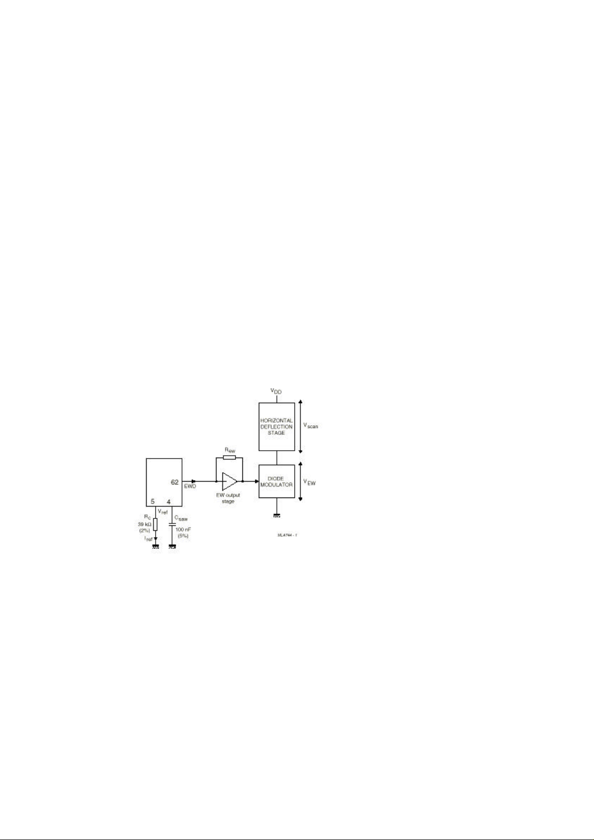
2.9. EAST – WEST OUTPUT STAGE
In order to obtain correct tracking of the vertical and horizontal EHT-correction, the EW output stage
should be dimensioned as illustrated in Figure. Resistor REW determines the gain of the EW output
stage. Resistor Rc determines the reference current for both the vertical sawtooth generator and the
geometry processor. The preferred value of Rc is 39 kW which results in a reference current of 100 mA
(Vref = 3.9 V).
The value of REW must be:
REW = RC * ( V
/ (18* V
scan
ref
) )
Example: With Vref = 3.9 V; Rc =39 kohm and Vscan = 120 V then REW =68 kohm
3. TUNER
PLL tuner is used as a tuner.
UV1316 (VHF/UHF) is used as a PLL tuner. For only PALM/N, NTSC M applications UV 1336 are used as the
PLL tuner.
Channel coverage of UV1316:
OFF-AIR CHANNELS CABLE CHANNELS
BAND
FREQUENCY
RANGE (MHz)
Low Band E2 to C 48.25 to 82.25 (1) S01 to S08
69.25 to 154.25
CHANNELS FREQUENCY CHANNELS
RANGE (MHz)
Page 10

Mid Band E5 to E12 175.25 to 224.25 S09 to S38
161.25 to 439.25
High Band E21 to E69 471.25 to 855.25 (2) S39 to S41
447.25 to 463.25
(1). Enough margin is available to tune down to 45.25 MHz.
(2). Enough margin is available to tune up to 863.25 MHz.
Noise Typical Max. Gain Min. Typical
Low band : 5dB 9dB All channels : 38dB 44dB
Mid band : 5dB 9dB Gain Taper (of-air channels) : - -
High band : 6dB 9dB
Channel Coverage UV1336:
BAND CHANNELS FREQUENCY
Low Band 2 to D 55.25 to 139.25
Mid Band E to PP 145.25 to 391.25
High Band QQ to 69 397.25 to 801.25
Noise is typically 6dB for all channels. Gain is minimum 38dB and maximum 50dB for all channels.
4. VIDEO SWITCH TEA6415C
In case of three or more external sources are used, the video switch IC TEA6415C is used. The main function of
this device is to switch 8 video-input sources on the 6 outputs.
Each output can be switched on only one of each input. On each input an alignment of the lowest level of the
signal is made (bottom of sync. top for CVBS or black level for RGB signals).
Each nominal gain between any input and output is 6.5dB.For D2MAC or Chroma signal the alignment is
switched off by forcing, with an external resistor bridge, 5VDC on the input. Each input can be used as a normal
input or as a MAC or Chroma input (with external Resistor Bridge). All the switching possibilities are changed
through the BUS.
Driving 75ohm load needs an external resistor.
It is possible to have the same input connected to several outputs.
Max.
52dB
8dB
RANGE (MHz)
5. MULTI STANDARD SOUND PROCESSOR
The MSP 34x0D is designed to perform demodulation of FM or AM-Mono TV sound. Alternatively, two-carrier
FM systems according to the German or Korean terrestrial specs or the satellite specs can be processed with the
MSP 34x0D. Digital demodulation and decoding of NICAM-coded TV stereo sound, is done only by the MSP
3410. The MSP 34x0D offers a powerful feature to calculate the carrier field strength which can be used for
automatic standard detection (terrestrial) and search algorithms (satellite).
6. SOUND OUTPUT STAGE WITH TDA 7265
TDA7265 is a class AB dual Audio power amplifier assembled in the multiwatt package.
Mute stand-by function of the audio amplifier can be described as the following; the pin 5
(MUTE/STAND-BY) controls the amplifier status by two different thresholds, referred to +Vs. When
Vpin (5) higher than (+Vs - 2.5V) the amplifier is in Stand-by mode and the final stage generators are
off. When Vpin (5) is between (+Vs – 2.5V) and (+Vs – 6V) the final stage current generators are
switched on and the amplifier is in mute mode. When the Vpin (5) is lower than +Vs – 6V the amplifier
is play mode.
Page 11

7. VERTICAL OUTPUT STAGE WITH STV 9379
The IC TDA9379FA is the vertical deflection booster circuit. Two supply voltages, +12V and –12V are
needed to scan the inputs VERT+ and VERT-, respectively. And a third supply voltage, +45V for the
flyback limiting are needed. The vertical deflection coil is connected in series between the output and
feedback to the input.
8. VIDEO OUTPUT AMPLIFIER TDA6108
The TDA6107/08Q includes three video output amplifiers in a SIL 9 MP (Single in Line 9 pins Medium Power)
package SOT111BE, using high-voltage DMOS technology, and is intended to drive the three cathodes of a colour
picture tube.
In contrast to previous types of DMOS video amplifiers, all external resistors (Rf, Ri and Ra) are integrated, so the
gain is fixed.
To obtain maximum performance, the amplifier should be used with black-current control and mounted on the
CRT panel.
9. COMBFILTER TDA 9181
The TDA 9181 is an adaptive PAL/NTSC comb filter with two internal delay lines, filters, clock
control, and input clamps. Video standards PAL B, G, H, I, M and N NTSC M are supported.
Two CVBS input signals can be selected by means of input switch.
In addition to the comb filter the circuit contains an output switch so that a selection can be made between the
combed CVBS signal and an external Y/C signal.
The supply voltage is 5V.
10. POWER SUPPLY (SMPS)
The DC voltages required at various parts of the chassis are provided by an SMPS transformer controlled by the IC
MC44608, which is designed for driving, controlling and protecting switching transistor of SMPS. The transformer
produces 150V for FBT input, ?14V for audio output IC, S+3.3, S+5V and 8V for TDA8885.
11. POWER FACTOR CORRECTION
The MC33260 is a controller for Power Factor Correction pre-converters meeting international
standard requirements in electronic ballast and off–line power conversion applications. Designed to
drive a free frequency discontinuous mode, it can also be synchronised and in any case, it features very
effective protections that ensure a safe and reliable operation.
12. MICROCONTROLLER SDA555X
12.1. General Features
• Feature selection via special function register
• Simultaneous reception of TTX, VPS, PDC, and WSS (line 23)
• Supply Voltage 2.5 and 3.3 V
• ROM version package P-SDIP 52
• ROMless version package P-LCC84
12.2. External Crystal and Programmable clock speed
• Single external 6MHz crystal, all necessary clocks are generated internally
• CPU clock speed selectable via special function registers.
• Normal Mode 33.33 MHz CPU clock, Power Save mode 8.33 MHz
12.3. Microcontroller Features
• 8bit 8051 instruction set compatible CPU.
• 33.33-MHz internal clock (max.)
• 0.360 ms (min.) instruction cycle
• Two 16-bit timers
• Watchdog timer
• Capture compare timer for infrared remote control decoding
• Pulse width modulation unit (2 channels 14 bit, 6 channels 8 bit)
• ADC (4 channels, 8 bit)
• UART
Page 12

12.4. Memory
• Non-multiplexed 8-bit data and 16 … 20-bit address bus (ROMless Version)
• Memory banking up to 1Mbyte (ROMless version)
• Up to 128 Kilobyte on Chip Program ROM
• Eight 16-bit data pointer registers (DPTR)
• 256-bytes on-chip Processor Internal RAM (IRAM)
• 128bytes extended stack memory.
• Display RAM and TXT/VPS/PDC/WSS-Acquisition-Buffer directly accessible via MOVX
• UP to 16KByte on Chip Extended RAM (XRAM) consisting of;
- 1 Kilobyte on-chip ACQ-buffer-RAM (access via MOVX)
- 1 Kilobyte on-chip extended-RAM (XRAM, access via MOVX) for user software
- 3 Kilobyte Display Memory
12.5. Display Features
• ROM Character set supports all East and West European Languages in single device
• Mosaic Graphic Character Set
• Parallel Display Attributes
• Single/Double Width/Height of Characters
• Variable Flash Rate
• Programmable Screen Size (25 Rows x 33...64 Columns)
• Flexible Character Matrixes (HxV) 12 x 9...16
• Up to 256 Dynamical Redefinable Characters in standard mode; 1024 Dynamical
Redefinable Characters in Enhanced Mode
• CLUT with up to 4096 colour combinations
• Up to 16 Colours per DRCS Character
• One out of Eight Colours for Foreground and Background Colours for 1-bit DRCS and
12.6. ROM Characters
• Shadowing
• Contrast Reduction
• Pixel by Pixel Shiftable Cursor With up to 4 Different Colours
• Support of Progressive Scan and 100 Hz.
• 3 X 4Bits RGB-DACs On-Chip
• Free Programmable Pixel Clock from 10 MHz to 32MHz
• Pixel Clock Independent from CPU Clock
• Multinorm H/V-Display Synchronisation in Master or Slave Mode
12.7. Acquisition Features
• Multistandard Digital Data Slicer
• Parallel Multi-norm Slicing (TTX, VPS, WSS, CC, G+)
• Four Different Framing Codes Available
• Data Caption only limited by available Memory
• Programmable VBI-buffer
• Full Channel Data Slicing Supported
• Fully Digital Signal Processing
• Noise Measurement and Controlled Noise Compensation
• Attenuation Measurement and Compensation
• Group Delay Measurement and Compensation
• Exact Decoding of Echo Disturbed Signals
12.8. Ports
• One 8-bit I/O-port with open drain output and optional I 2 C Bus emulation support (Port0)
• Two 8-bit multifunction I/O-ports (Port1, Port3)
• One 4-bit port working as digital or analogue inputs for the ADC (Port2)
• One 2-bit I/O port with secondary functions (P4.2, 4.3, 4.7)
• One 4-bit I/O-port with secondary function (P4.0, 4.1, 4.4) (Not available in P-SDIP 52)
Page 13

13. SERIAL ACCESS CMOS 8K (1024*8) EEPROM ST24C08
The ST24C08 is a 8Kbit electrically erasable programmable memory (EEPROM), organised as 4 blocks of 256*8
bits.
The memory is compatible with the I²C standard, two wire serial interface, which uses a bi-directional data bus and
serial clock.
The memory carries a built-in 4 bit, unique device identification code (1010) corresponding to the I²C bus
definition.
This is used together with 1 chip enable input (E) so that up to 2*8K devices may be attached to the I²C bus and
selected individually.
14. CLASS AB STEREO HEADPHONE DRIVER TDA1308
The TDA1308 is an integrated class AB stereo headphone driver contained in a DIP8 plastic package.
The device is fabricated in a 1 mm CMOS process and has been primarily developed for portable digital audio
applications.
15. SAW FILTERS
Saw filter type : Model:
K9356M : PAL-SECAM B/G/D/K/I STEREO (AUDIO IF)
K9656M : PAL-SECAM B/G/D/K/I/L/L’ STEREO (AUDIO IF)
K3958M : PAL-SECAM B/G/D/K/I/L/L’ STEREO (VIDEO IF)
16. IC DESCRIPTIONS AND INTERNAL BLOCK DIAGRAM
? TDA8885
? TUNER (UV1315, UV1316)
? TEA6415C
? TDA 7265
? TDA6108Q
? 74HCT32
? MC44608
? SDA5555
? TDA9181
? TCD1102
? ST24C08
? TDA1308
? PCF8583
? MC33260
? STV9379
? MSP34XXG
? LM358N
16.1. TDA8885:
16.1.1. GENERAL DESCRIPTION
The TDA 8885 is I 2 C-bus controlled singlechip TV processors, which are intended to be applied in
PAL/NTSC and multi-standard television receivers. These ICs are largely compatible with the TDA
884X/5X series. Also in this IC family we have versions with a mono intercarrier FM sound channel and
versions with a QSS IF amplifier.
The main difference between the TDA 884X/5X series and the TDA 886X/7X/8X series is that the latter
contains integrated sound band-pass (in mono FM versions) and trap circuits, a switchable group delay
correction circuit and a multi-standard colour decoder which needs only one inexpensive (12 MHz) reference
crystal for all standards.
Furthermore various picture improvement features have been included.
16.1.2. FEATURES
• Multi-standard vision IF circuit with an alignment-free PLL demodulator without external components
• Internal (switchable) time-constant for the IF-AGC circuit
• Switchable sound trap and group delay correction circuit for the demodulated CVBS signal
• Flexible source selection with CVBS switch and a Y (CVBS)/C input so that a comb filter can be
applied
• Integrated chrominance trap circuit
• Integrated luminance delay line with adjustable delay time
• Integrated chroma band-pass filter with switchable centre frequency
Page 14

• Colour decoder which needs only one 12 MHz reference crystal (or external clock signal) for all
standards
• Blanking of the ‘helper signals’ for PAL PLUS and EDTV-2
• Several picture improvement features.
• Internal base-band delay line
• YUV interface
• Linear RGB input and fast blanking
• RGB control circuit with ‘Continuous Cathode Calibration’, white point and black level offset
adjustment so that the colour temperature of the dark and the light parts of the screen can be chosen
independently.
• Adjustable peak white limiting circuit
• Half-tone (contrast reduction) possibility during mixed-mode of OSD and text signals
• Possibility to insert a ‘blue back’ option when no video signal is available
• Horizontal synchronisation with two control loops and alignment-free horizontal oscillator
• Vertical count-down circuit
• Vertical driver optimised for DC-coupled vertical output stages for improved geometry
• Vertical geometry processing.
• Low-power start-up for the horizontal drive circuit
• I 2 C-bus control of various functions
• QSS sound IF amplifier
• AM sound demodulator
• PAL decoder
• SECAM decoder
• NTSC decoder
• Additional RGB/ YUV input
• Black stretch and Blue stretch
• Dynamic skin tone control and coring on complete video signal
• Video dependent coring and Colour Transient Improvement
• White stretch and green enhancement
• Horizontal geometry (EW)
• Horizontal and vertical zoom
• Horizontal parallelogram and angle correction
• 2 nd CVBS output
• Additional YUV/ RGB input with saturation control
• 2 (I 2 C- bus controlled) switch outputs, which can be used to switch external circuits
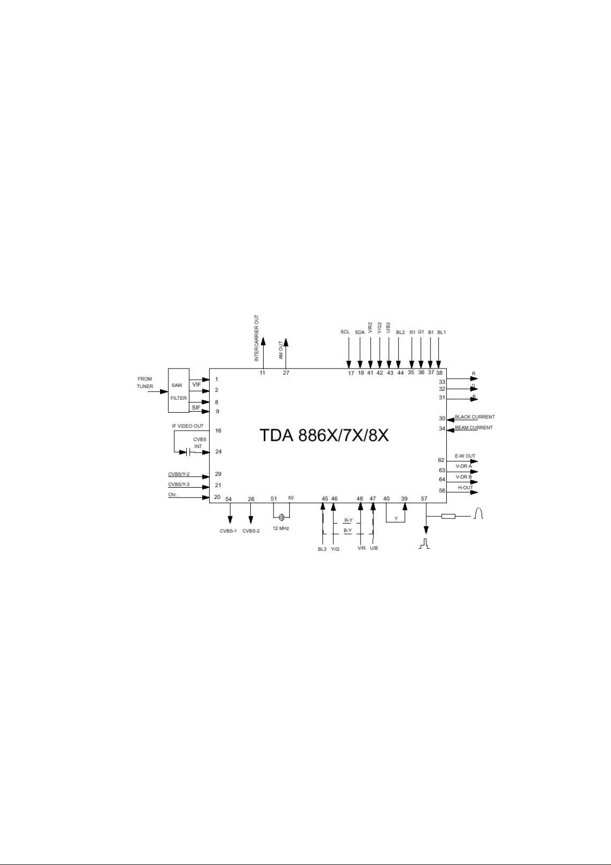
16.1.3. Pin Description
1 IF input 1
2 IF input 2
3 EHT/overvoltage protection input
4 vertical sawtooth capacitor
5 reference current input
6 ground (vision/QSS IF amplifier and sound)
7 tuner AGC output
8 de-emphasise (front-end sound out) or selected sound out or AM sound in (1) SIF input 1
9 decoupling sound demodulator SIF input 2
10 narrow-band PLL filter AGC sound IF
11 external audio input QSS intercarrier out or AM output or external audio input (2)
12 internally connected
13 half tone (contrast reduction)
14 low-power start-up
15 IF-PLL loop filter
16 IF video output
17 serial clock input
18 serial data input/output
19 white stretch capacitor
20 chrominance input (S-VHS)
21 external CVBS/Y 3 input
22 output switch 1 (I 2 C)
23 main supply voltage (+8V) (vision/QSS amplifier, filters, CTI and sound)
Page 15

24 internal CVBS input
25 ground 1 (colour decoder and synchronisation)
26 CVBS-2 output
27 audio out (volume controlled) / IF video out (3) AM audio output (volume controlled)
28 SECAM PLL decoupling
29 CVBS/Y 2 input
30 black-current input
31 blue output
32 green output
33 red output
34 beam current limiter input/V-guard input
35 red input for insertion
36 green input for insertion
37 blue input for insertion
38 RGB insertion input
39 luminance input
40 luminance output
41 2nd V/R input
42 2nd Y/G input
43 2nd U/B input
44 2nd RGB insertion input
45 U signal output or YUV-RGB insertion input (4)
46 V signal output or Y input or G input (4)
47 U or B signal input (4)
48 V or R signal input (4)
49 Ref. signal out or AVL or V-sync out (5) Ref. signal out or AM out or V-sync out (5)
50 decoupling digital supply
51 12 MHz crystal connection
52 12 MHz crystal connection
53 2nd supply voltage (+8 V) (colour decoder, control, synchronisation and geometry)
54 CVBS-1 output
55 bandgap decoupling
56 horizontal output
57 flyback input / sandcastle output
58 phase-2 filter
59 phase-1 filter
60 output switch 2 (I 2 C)
61 ground 2 (filters, CTI, control and geometry)
62 east-west drive output / Automatic Volume Levelling
63 vertical drive B output
64 vertical drive A output
SYMBOL PARAMETER MIN. TYP. MAX. UNIT
Supply
VP supply voltage 8.0 V
IP supply current tbf mA
Input voltages
Vi(VIF)(rms) video IF amplifier sensitivity (RMS value) 35 V
Vi(SIF)(rms) sound IF amplifier sensitivity (RMS value) 60 V
Vi(CVBS/Y)(p-p) external CVBS/Y input (peak-to-peak value) 1.0 V
Vi(CHROMA)(p-p) external chroma input voltage
(burst amplitude)(peak-to-peak value) 0.3 V
Vi(RGB)(p-p) RGB inputs (peak-to-peak value) 0.7 V
Vi(YI)(p-p) luminance input signal (peak-to-peak value) 1.4/1.0 V
Vi(UI)(p-p) U input signal (peak-to-peak value) 1.33/+0.7 V
Vi(VI)(p-p) V input signal (peak-to-peak value) 1.05/+0.7 V
Output signals
Vo(IFVO)(p-p) demodulated CVBS output (peak-to-peak value) 2.5 V
Io(AGCOUT) tuner AGC output current range 0 5 mA
Vo(QSSO)(rms) sound IF intercarrier output (RMS value) 100 mV
Vo(AMOUT)(rms) demodulated AM sound output (RMS value) 500 mV
Vo(CVBSO)(p-p) CVBS output voltage video switch (peak-to-peak value) 2.0 V
Vo(VO/I)(p-p) ?V output/input voltage (peak-to-peak value) 1.05 V
Page 16

Vo(UO/I)(p-p) ?U output/input voltage (peak-to-peak value) 1.33 V
Vo(YO/I)(p-p) Y output/input voltage (peak-to-peak value) 1.4 V
Vo(RGB)(p-p) RGB output signal amplitudes (peak-to-peak value) 2.0 V
Io(HOUT) horizontal output current 10 mA
Io(VERT) vertical output current (peak-to-peak value) 1 mA
Io(EWD) EW drive output current 1.2 mA
16.2. UV1315, UV1316
16.2.1. General description of UV1315:
The UV1315 tuner belongs to the UV 1300 familiy of tuners, which are designed to meet a wide range of
applications.
It is a combined VHF, UHF tuner suitable for CCIR systems B/G, H, L, L’, I and I’. The low IF output impedance
has been
designed for direct drive of a wide variety of SAW filters with sufficient suppression of triple transient.
16.2.2. Features of UV1315:
• Member of the UV1300 family small sized UHF/VHF tuners
• Systems CCIR:B/G, H, L, L’, I and I’; OIRT:D/K
• Voltage synthesised tuning (VST)
• Off-air channels, S-cable channels and Hyperband
• Standardised mechanical dimensions and pinning
• Compact size
PINNING PIN VALUE
1. Gain control voltage (AGC) : 4.0V, Max:4.5V
2. Tuning voltage
3. High band switch : 5V, Min:4.75V, Max:5.5V
4. Mid band switch : 5V, Min:4.75V, Max:5.5V
5. Low band switch : 5V, Min:4.75V, Max:5.5V
6. Supply voltage : 5V, Min:4.75V, Max:5.5V
7. Not connected
8. Not connected
9. Not connected
10. Symmetrical IF output 1
11. Symmetrical IF output 2
Bandswitching table:
Low band 0V 0V +5V
Mid band 0V +5V 0V
High band +5V 0V 0V
Pin 3 Pin 4 Pin 5
16.2.3. General description of UV1316:
The UV1316 tuner belongs to the UV 1300 family of tuners, which are designed to meet a wide range of
applications.
It is a combined VHF, UHF tuner suitable for CCIR systems B/G, H, L, L’, I and I’. The low IF output impedance
has been designed
for direct drive of a wide variety of SAW filters with sufficient suppression of triple transient.
16.2.4. Features of UV1316:
• Member of the UV1300 family small sized UHF/VHF tuners
• Systems CCIR: B/G, H, L, L’, I and I’; OIRT: D/K
• Digitally controlled (PLL) tuning via I2C-bus
• Off-air channels, S-cable channels and Hyperband
• World standardised mechanical dimensions and world standard pinning
Page 17

• Compact size
• Complies to “CENELEC EN55020” and “EN55013”
PINNING PIN VALUE
1. Gain control voltage (AGC) : 4.0V, Max:4.5V
2. Tuning voltage
3. I²C-bus address select : Max:5.5V
4. I²C-bus serial clock : Min:-0.3V, Max:5.5V
5. I²C-bus serial data : Min:-0.3V, Max:5.5V
6. Not connected
7. PLL supply voltage : 5.0V, Min:4.75V, Max:5.5V
8. ADC input
9. Tuner supply voltage : 33V, Min:30V, Max:35V
10. Symmetrical IF output 1
11. Symmetrical IF output 2
16.3. TEA6415C:
16.3.1. General Description:
The main function of the TEA6415C is to switch 8 video input sources on the 6 outputs.
Each output can be switched to only one of the inputs whereas but any same input may be connected to several
outputs.
All switching possibilities are controlled through the I2C-bus.
16.3.2. Features:
• 20 MHz Bandwidth
• Cascadable with another TEA6415C (Internal address can be changed by pin 7 voltage)
• 8 inputs (CVBS, RGB, Mac, CHROMA, …)
• 6 Outputs
• Possibility of MAC or chroma signal for each input by switching-off the clamp with an external resistor
bridge
• Bus controlled
• 6.5dB gain between any input and output
• -55dB crosstalk at 5MHz
• Fully ESD protected
PINNING PIN VALUE
1. Input : Max : 2Vpp, Input Current : 1mA, Max : 3mA
2. Data : Low level : -0.3V Max:1.5V, High level : 3.0V Max :
Vcc+0.5V
3. Input : Max : 2Vpp, Input Current : 1mA, Max : 3mA
4. Clock : Low level : -0.3V Max:1.5V, High level : 3.0V Max :
Vcc+0.5V
5. Input : Max : 2Vpp, Input Current : 1mA, Max : 3mA
6. Input : Max : 2Vpp, Input Current : 1mA, Max : 3mA
7. Prog
8. Input : Max : 2Vpp, Input Current : 1mA, Max : 3mA
9. Vcc : 12V
10. Input : Max : 2Vpp, Input Current : 1mA, Max : 3mA
11. Input : Max : 2Vpp, Input Current : 1mA, Max : 3mA
12. Ground
13. Output : 5.5Vpp, Min : 4.5Vpp
14. Output : 5.5Vpp, Min : 4.5Vpp
15. Output : 5.5Vpp, Min : 4.5Vpp
16. Output : 5.5Vpp, Min : 4.5Vpp
17. Output : 5.5Vpp, Min : 4.5Vpp
18. Output : 5.5Vpp, Min : 4.5Vpp
19. Ground
20. Input : Max : 2Vpp, Input Current : 1mA, Max : 3mA
Page 18

16.4. TDA7265:
The TDA7265 is a 25W+25W stereo sound amplifier with mute/stand-by facility. STPA control signal coming
from microcontroller (when it is at high level) activates the mute function. IC is muted when mute port is at low
level. Two stereo audio signals coming from audio module is injected to the inputs of the IC and a power of
12Wrms (10%) is obtained. An external pop-noise circuitry pulls AF inputs of the IC in order to eliminate pop
noise when TV is turned on or off via mains supply connection. It is possible to adjust the gain of the amplifiers by
feedback external resistors.
16.4.1. Features:
• Wide supply voltage range (up to 50V ABS Max.)
• Split supply
• High output power: 25+25 W @ TDA = 10%, RL = 8ohm, VS = ±20V
• No pop at turn-on / off
• Mute (pop free)
• Stand-By feature (low IQ)
• Few external components
• Thermal overload protection
• Adjustable gain via an external resistor
16.4.2. Pinning:
1. Output (1)
2. +Vs
3. Output (2)
4. Mute / St-By
5. -Vs
6. Input (2)
7. Ground
8. Input (1)
16.5. TDA6108Q:
The TDA6108Q consists of three monolithic video output amplifiers. The amplifier can be seen as an operational
amplifier with negative feedback. The advantage of negative feedback is that the amplifier characteristics do not
play an important role up to certain frequencies. The internal flash diodes protect the amplifiers against flash over
in the picture tube. The only protections required at the cathode outputs are a flash resistor and a spark gap.
Furthermore, the device needs only one power supply voltage (Vdd). The TDA6108Q is provided with a black
current data pin.
16.5.1. Features:
• No external components, only the well known supply decoupling
• Very simple application with a variety of colour decoders
• Black-current measurement output for automatic black current stabilisation
• Only one supply voltage needed
• Internal protection against positive appearing CRT flash-over discharges
• Protection against ESD
• Internal reference voltage
• Thermal protection
• Controllable switch-off behaviour
• Very small PCB dimensions
• Very high replacement value
PINNING PIN VALUE
1. Inverting input 1 :2Vpp
2. Inverting input 2 :2Vpp
3. Inverting input 3 :2Vpp
4. Ground
5. BSC-output :Max:7V
Page 19

6. Supply voltage :200VDC
7. Cathode output 3 :20mA, 100Vpp
8. Cathode output 2 :20mA, 100Vpp
9. Cathode output 1 :20mA, 100Vpp
16.6. 74 HCT 32
The 74HC/HCT32 are high-speed Si-gate CMOS devices and are pin compatible with low power Schottky
TTL (LSTTL). They are specified in compliance with JEDEC. The 74HC/HCT32 provide the 2-input OR
function.
16.6.1. PINNING
1, 4, 9, 12 : 1A to 4A data inputs
2, 5, 10, 13 : 1B to 4B data inputs
3, 6, 8, 11 : 1Y to 4Y data outputs
7 : GND ground (0 V)
14 : VCC positive supply voltage
For HC the condition is VI = GND to VCC
For HCT the condition is VI = GND to VCC ??1.5 V
16.7. MC44608
16.7.1. General description:
The MC44608 is a high performance voltage mode controller designed for off–line converters. This
high voltage circuit that integrates the start–up current source and the oscillator capacitor, requires few
external components while offering a high flexibility and reliability.
The device also features a very high efficiency stand–by management consisting of an effective Pulsed Mode
operation. This technique enables the reduction of the stand–by power consumption to approximately 1W while
delivering 300mW in a 150W SMPS.
• Integrated start–up current source
• Lossless off–line start–up
• Direct off–line operation
• Fast start–up
16.7.2. General Features
• Flexibility
• Duty cycle control
• On chip oscillator switching frequency 40, or 75kHz
• Secondary control with few external components
Protections
• Maximum duty cycle limitation
• Cycle by cycle current limitation
• Demagnetisation (Zero current detection) protection
• “Over V CC protection” against open loop
• Programmable low inertia over voltage protection against open loop
• Internal thermal protection
GreenLine Controller
• Pulsed mode techniques for a very high efficiency low power mode
• Lossless start-up
• Low dV/dT for low EMI radiation's
PINNING PIN VALUE
1. Demagnetisation Zero cross detection voltage: 50 mV typ.
2. I Sense Over current protection voltage 1V typ.
Page 20

3. Control Input Min: 7.5V Max.: 18V
4. Ground Iout 2A
during scan 1.2A
p-p
during flyback
p-p
5. Driver Output resistor 8.5 Ohm sink 15 Ohm source typ.
6. Supply voltage Max:16V (Operating range 6.6V-13V)
7. No connection
8. Line Voltage Min:50V Max:500V
16.8. SDA5555:
16.8.1. General description:
• Feature selection via special function register
• Simultaneous reception of TTX, VPS, PDC, and WSS (line 23)
• Supply Voltage 2.5 and 3.3 V
PINNING
1 Comb Filter Standard Selection 1 Low Level : 0V High Level : 3.3 V
2 Key 2 Low Level : 0V High Level : 3.3 V
3 Key 1 Low Level : 0V High Level : 3.3 V
4 Loc.key.switch input Low Level : 0V High Level : 3.3 V
5 Loc.key.switch input Low Level : 0V High Level : 3.3 V
6 Loc.key.switch input Low Level : 0V High Level : 3.3 V
7 Loc.key.switch input Low Level : 0V High Level : 3.3 V
8 Mute output Low Level : 0V High Level : 3.3 V
9 Digital supply voltage 2.5 V
10 Ground
11 Digital supply voltage 3.3 V
12 CVBS input 1 Vpp
13 Analogue supply voltage 2.5 V
14 Analogue ground
15 Wake Interrupt Low Level : 0V High Level : 3.3 V
16 AV-1 status input Low Level : 0V High Level : 3.3 V
17 AV-2 status input Low Level : 0V High Level : 3.3 V
18 Shortcut protection Low Level : 0V High Level : 3.3 V
19 SAND input Low Level : 0V High Level : 3.3 V
20 ODD/EVEN output Low Level : 0V High Level : 3.3 V
21 DVD 12 V Sense Low Level : 0V High Level : 3.3 V
22 Not used
23 Idle Off Low Level : 0V High Level : 3.3 V
24 IR-input Low Level : 0V High Level : 3.3 V
25 Data output Low Level : 0V High Level : 3.3 V
26 Clock signal output Low Level : 0V High Level : 3.3 V
27 Stand-By Mode selection Low Level : 0V High Level : 3.3 V
28 Not used
29 Ground
30 Digital supply voltage 3.3 V
31 Write Protect output Low Level : 0V High Level : 3.3 V
32 Service output Low Level : 0V High Level : 3.3 V
33 Reset output Low Level : 0V High Level : 3.3 V
34 6 MHz cristal connection 2 Low Level : 0V High Level : 3.3 V
35 6 MHz cristal connection 1 Low Level : 0V High Level : 3.3 V
36 Analogue ground
37 Analogue supply voltage 2.5 V
38 OSD-Red output 0.7 Vpp to 1.2 Vpp
Page 21

39 OSD-Green output 0.7 Vpp to 1.2 Vpp
40 OSD-Blue output 0.7 Vpp to 1.2 Vpp
41 OSD-Blanking output Low Level : 0V High Level : 3.3 V
42 Digital supply voltage 2.5 V
43 Ground
44 Digital supply voltage 3.3 V
45 PAL / SECAM Low Level : 0V High Level : 3.3 V
46 Degauss Low Level : 0V High Level : 3.3 V
47 Horizontal Trapezoid Low Level : 0V High Level : 3.3 V
48 Tilt Low Level : 0V High Level : 3.3 V
49 Not used
50 Micro s. select Low Level : 0V High Level : 3.3 V
51 Comb Filter Standard Selection 2 Low Level : 0V High Level : 3.3 V
52 SVHS Sense Low Level : 0V High Level : 3.3 V
16.9. TDA9181:
Pin#:
Pin-1 = Cýn=Chrominance input signal
Pin-2 = INPSEL=input switch select input
Pin-3 =Y/CVBS2=luminance or CVBS input signal 2
Pin-4 = Digital GND
Pin-5= VDD=digital supply voltage
Pin-6=VCC=analog supply voltage
Pin-7 =SC=sandcastle input signal
Pin-8 =FSCSEL=color subcarrier select input
Pin-9 = FSC=color subcarrier input signal
Pin-10 =SYS2=standart select 2 input
Pin-11 = SYS1=standart select 1 input
Pin-12 =Y/CVBS1=luminance or CVBS input signal
Pin-13 = analogue GND
Pin-14 = Y/CVBSout=luminance or CVBS output signal
Pin-15 =OUTSEL=output switch select input
Pin-16 =Cout=chrominance output signal
16.9.1. General Features:
-One chip multistandart adaptive comb filter
-Cross luminance reduction
-Cross colour reduction
-No chroma trap, so sharper vertical luminance
-Analogue discrete-time signal processing, so no quantization noise
-Anti aliasing and reconstruction filters are included
-Input switch selects between two Y/CVBS inputs
-Output switch selects between combed CVBS and an external Y/C source
-Fsc as well as 2*fsc colour subcarrier signal may be applied
-Alignment free
-Few external components
-Low power
16.9.2. Limits:
-Analogue supply voltage Vcc=5.5V(max)
-Analogue supply current Icc=25mA(typ)
-Digital supply voltage Vdd=5.5(V)(max)
-Digital supply current Idd=10Ma(typ)
-Luminance or CVBS input signal (p-p) Y/CVBS1, 2 1.4V(max)
Page 22

-Chrominance input signal (p-p) Cin=1.0V(max)
16.10. TCD1102:
16.10.1. Description
The TCET110./ TCET2100/ TCET4100 consists of a phototransistor optically coupled to a gallium
arsenide infrared emitting diode in a 4-lead plastic dual inline package. The elements are mounted on
one leadframe using a
coplanar technique, providing a fixed distances between input and output for highest safety
requirements.
16.10.2. Applications
Circuits for safe protective separation against electrical shock according to safety class II (reinforced
isolation):
For appl. class I – IV at mains voltage ?300 V
For appl. class I – III at mains voltage ?600 V
according to VDE 0884, table 2, suitable for:
Switch-mode power supplies, line receiver, computer
peripheral interface, microprocessor system interfaces.
VDE 0884 related features:
Rated impulse voltage (transient overvoltage) V IOTM = 8 kV peak
Isolation test voltage (partial discharge test voltage) V pd = 1.6 kV
Rated isolation voltage (RMS includes DC) V IOWM = 600 V RMS (848 V peak)
Rated recurring peak voltage (repetitive) V IORM = 600 V RMS
16.10.3. General features:
CTR offered in 9 groups
Isolation materials according to UL94-VO
Pollution degree 2 (DIN/VDE 0110 / resp. IEC 664)
Climatic classification 55/100/21 (IEC 68 part 1)
Special construction: Therefore, extra low coupling capacity of typical 0.2 pF, high Common Mode
Rejection
Low temperature coefficient of CTR
G = Leadform 10.16 mm; provides creepage distance > 8 mm, for TCET2100/ TCET4100 optional;
suffix letter ‘G’ is not marked on the optocoupler
Coupling System U
16.11. ST24C08:
16.11.1. General description:
The ST24C08 is an 8Kbit electrically erasable programmable memory (EEPROM), organised as 4 blocks of 256 *
8 bits.
The memory operates with a power supply value as low as 2.5V. Both Plastics Dual-in-Line and Plastic Small
Outline packages
are available.
16.11.2. Features:
• Minimum 1 million ERASE/WRITE cycles with over 10 years data retention
• Single supply voltage:4.5 to 5.5V
• Two wire serial interface, fully I2C-bus compatible
• Byte and Multibyte write (up to 8 bytes)
Page 23

• Page write (up to 16 bytes)
• Byte, random and sequential read modes
• Self timed programming cycle
PINNING PIN VALUE
1. Write protect enable (Ground) : 0V
2. Not connected (Ground) : 0V
3. Chip enable input (Ground) : 0V
4. Ground : 0V
5. Serial data address input/output : Input LOW voltage : Min : -0.3V, Max : 0.3*Vcc
6. Serial clock : Input LOW voltage : Min: -0.3V, Max : 0.3*Vcc
7. Multibyte/Page write mode : Input LOW voltage : Min: -0.3V, Max :0.5V
8. Supply voltage : Min : 2.5V, Max : 5.5V
Input HIGH voltage: Min : 0.7*Vcc, Max : Vcc+1
Input HIGH voltage: Min : 0.7*Vcc, Max : Vcc+1
Input HIGH voltage: Min : Vcc-0.5, Max : Vcc+1
16.12. TDA1308:
16.12.1. Features:
• Wide temperature range
• No switch ON/OFF clicks
• Excellent power supply ripple rejection
• Low power consumption
• Short-circuit resistant
• High performance
- high signal-to-noise ratio
- high slew rate
- low distortion
• Large output voltage swing
PINNING PIN VALUE
1. Output A (Voltage swing) : Min : 0.75V, Max : 4.25V
2. Inverting input A : Vo(clip) : Min : 1400mVrms
3. Non-inverting input A : 2.5V
4. Ground : 0V
5. Non-inverting input B : 2.5V
6. Inverting input B : Vo(clip) : Min : 1400mVrms
7. Output B (Voltage swing) : Min : 0.75V, Max : 4.25V
8. Positive supply : 5V, Min : 3.0V, Max : 7.0V
16.13. PCF8583:
16.13.1. FEATURES
• I 2 C-bus interface operating supply voltage: 2.5 V to 6 V
• Clock operating supply voltage (0 to +70 ?C):1.0 V to 6.0 V
• 240 8-bit low-voltage RAM
• Data retention voltage: 1.0 V to 6 V
• Operating current (at fSCL = 0 Hz): max. 50 ?A
• Clock function with four year calendar
• Universal timer with alarm and overflow indication
• 24 or 12 hour format
• 32.768 kHz or 50 Hz time base
• Serial input/output bus (I 2 C)
• Automatic word address incrementing
• Programmable alarm, timer and interrupt function
• Slave address:
– READ: A1 or A3
– WRITE: A0 or A2.
Page 24

16.13.2. GENERAL DESCRIPTION
The PCF8583 is a clock/calendar circuit based on a 2048-bit static CMOS RAM organised as 256 words by
8 bits. Addresses and data are transferred serially via the two-line bi-directional I 2 C-bus. The built-in word
address register is incremented automatically after each written or read data byte. Address pin A0 is used for
programming the hardware address, allowing the connection of two devices to the bus without additional
hardware. The built-in 32.768 kHz oscillator circuit and the first 8 bytes of the RAM are used for the
clock/calendar and counter functions. The next 8 bytes may be programmed as alarm registers or used as free
RAM space. The remaining 240 bytes are free RAM locations.
SYMBOL PIN DESCRIPTION
OSCI 1 oscillator input, 50 Hz or event-pulse input
OSCO 2 oscillator output
A0 3 address input
VSS 4 negative supply
SDA 5 serial data line
SCL 6 serial clock line
INT 7 open drain interrupt output (active LOW)
VDD 8 positive supply
16.14. MC33260:
16.14.1. General Features:
-Standard Constant Output Voltage or “Follower Boost” Mode
-Switch Mode Operation: Voltage Mode
-Latching PWM for Cycle–by–Cycle On–Time Control
-Constant On–Time Operation That Saves the Use of an Extra Multiplier
-Totem Pole Output Gate Drive
-Undervoltage Lockout with Hysteresis
-Low Start–Up and Operating Current
-Improved Regulation Block Dynamic Behaviour
-Synchronisation Capability
-Internally Trimmed Reference Current Source
16.14.2. Safety Features:
-Overvoltage Protection: Output Overvoltage Detection
-Undervoltage Protection: Protection Against Open Loop
-Effective Zero Current Detection
-Accurate and Adjustable Maximum On–Time Limitation
-Overcurrent Protection
-ESD Protection on Each Pin
16.14.3. LIMITS:
-Vcc MAX voltage 16V
-Gate drive current source=-500mA, sink=500mA
-Input voltage –0.3V to +1.0V
-Operating junction Temperature +150 C
16.14.4. PINNING
Pin1=Feedback input
Pin2=Vcontrol
Pin3=Oscillator capacitor(Ct)
Page 25

Pin4=Current Sense Input
Pin5=Synchronization Input
Pin6=GND
Pin7=Gate Drive
Pin8=Vcc
16.15. STV9379:
16.15.1. DESCRIPTION
Designed for monitors and high performance TVs, the STV9379FA vertical deflection booster can
handle flyback voltage up to 90V. Further to this, it is possible to have a flyback voltage, which is more
than the double of the supply (Pin 2). This allows to decrease the power consumption, or to decrease
the flyback time for a given supply voltage.
The STV9379FA operates with supplies up to 42V and provides up to 2.6APP output current to drive
the yoke.
The STV9379FA is offered in HEPTAWATT package.
16.15.2. PINNING
Pin1 : Output Stage Supply
Pin2 : Output
Pin3 : GND or Negative Supply
Pin4 : Flyback Supply
Pin5 : Supply Voltage
Pin6 : Inverting Input
Pin7 : Non-inverting Input
16.16. MSP34XX :
MSP3410D
The MSP3410D is an I2C controlled single-chip multistandard sound processor for applications in analog and
digital TV sets. The full TV sound processing, starting with analog sound IF signal-in, down to processed analog
AF-out is performed in a single-chip covering all European TV-standards. It is designed to simultaneously perform
digital demodulation and decoding of NICAM-coded TV stereo sound, as well as demodulation of FM-mono TV
sound and two FM systems according to the German or Korean terrestrial specs. It is also possible to do AMdemodulation according to the SECAM system. There is AGC for analog inputs: 0.14 - 3Vpp. All demodulation
and filtering is performed on chip and is individually programmable. All digital NICAM standards (B/G, L, and I)
are realised. Only one crystal clock (18.432Mhz) is necessary. External capacitors at each crystal pin to ground are
required. They are necessary for tuning the open-loop frequency of the internal PLL and for stabilising the
frequency in closed-loop operation. The higher the capacitors, the lower the clock frequency result. The nominal
free running frequency should match the centre of the tolerance range between 18.433 and 18.431Mhz as closely
as possible. By means of standardised I2S interface, additional feature processors (DPL35xx, Dolby Prologic
processor for this chassis) can be connected to the IC.
I2S bus interface consists of five pins:
I2S_DA_IN1…2 for input four channels (two channels per line) per sampling cycle (32Khz).
I2DA_OUT, for output, two channels per sampling cycle (32KHz).
I2S_CL, for timing of the transmission of I2S serial data, 1.024Mhz.
I2S_WS, for the word strobe line defining the left and right sample.
Features:
n 5-band graphic equalizer (as in MSP3400C)
n Enhanced spatial affect (pseudo stereo / base-width enlargement as in MSP3400C)
n Headphone channel with balance, bass treble, loudness
n Balance for loudspeaker and headphone channels in dB units (optional)
Page 26

n Additional pair of D/A converters for SCART2 out
n Improved over-sampling filters (as in MSP 3400C)
n Additional SCART input
n Full SCART in/out matrix without restrictions
n SCART volume in dB units (optional)
n Additional I²S input (as in MSP 3400C)
n New FM-identification (as in MSP 3400C)
n Demodulator short programming
n Auto-detection for terrestrial TV-sound standards
n Precise bit-error rate indication
n Automatic switch from NICAM to FM/AM or vice versa
n Improved NICAM synchronisation algorithm
n Improved carrier mute algorithm
n Improved AM-demodulation
n ADR together with DRP 3510A
n Dolby Pro Logic together with DPL 35xx A
n Reduction of necessary controlling
n Less external components
n Significant reduction of radiation
Pinning:
1. ADR wordstrobe 35. Analog Shield Ground 1
2. Not connected 36. Scart input 3 in right
3. ADR data output 37. Scart input 3 in left
4. I²S 1 data input 38. Analog Shield Ground 4
5. I²S data output 39. Scart input 4 in, right
6. I²S wordstrobe 40. Scart input 4 in, left
7. I²S clock 41. Not connected
8. I²S data 42. Analog reference voltage high voltage part
9. I²S clock 43. Analog ground
10. Not connected 44. Volume capacitor MAIN
11. Standby (low-active) 45. Analog power supply 8.0V
12. I²C Bus address select 46. Volume capacitor AUX
13. Digital control output 0 47. Scart output 1, left
14. Digital control output 1 48. Scart output 1, right
15. Not connected 49. Reference ground 1 high voltage part
16. Not connected 50. Scart output 2, left
17. Not connected 51. Scart output 2, right
18. Audio clock output 52. Analog Shield Ground 3
19. Not connected 53. Not connected
20. Crystal oscillator 54. Not connected
21. Crystal oscillator 55. Not connected
22. Test Pin 56. Analog output MAIN, left
23. IF input 2 (if ANA_IN1+is used only, connect 57. Analog output MAIN, right to AVSS with
50 pF capacitor) 58. Reference ground 2 high voltage part
24. IF common 59. Analog output AUX, left
25. IF input 1 60. Analog output AUX, right
26. Analog power supply +5V 61. Power-on-reset
27. Analog ground 62. Not connected
28. Mono input 63. Not connected
29. Reference voltage IF A/D converter 64. Not connected
30. Scart input 1 in, right 65. I²S2-data input
31. Scart input 1 in, left 66. Digital ground
32. Analog Shield Ground 2 67. Digital power supply +5V
33. Scart input 2 in, right 68. ADR clock
34. Scart input 2 in, left
Page 27

16.17. LM358N:
16.17.1. General Description
The LM158 series consists of two independent, high gain, internally frequency compensated operational amplifiers
which were designed specifically to operate from a single power supply over a wide range of voltages. Operation from
split power supplies is also possible and the low power supply current drain is independent of the magnitude of the power
supply voltage. Application areas include transducer amplifiers, dc gain blocks and all the conventional op amp circuits,
which now can be more easily implemented in single power supply systems. For example, the LM158 series can be
directly operated off of the standard +5V power supply voltage, which is used in digital systems and will easily provide
the required interface electronics without requiring the additional ±15V power supplies.
16.17.2. Unique Characteristics
In the linear mode the input common-mode voltage range includes ground and the output voltage can also swing to
ground, even though operated from only a single power supply voltage.
The unity gain cross frequency is temperature compensated.
The input bias current is also temperature compensated.
16.17.3. Advantages
Two internally compensated op amps
Eliminates need for dual supplies
Allows direct sensing near GND and VOUT also goes to GND
Compatible with all forms of logic
Power drain suitable for battery operation
Pin-out same as LM1558/LM1458 dual op amp
16.17.4. Features
Available in 8-Bump micro SMD chip sized package, Internally frequency compensated for unity gain n Large dc
voltage gain: 100 dB
Wide bandwidth (unity gain): 1 MHz (temperature compensated)
Wide power supply range:
Very low supply current drain (500 µA) —essentially independent of supply voltage
Low input offset voltage: 2 mV
Input common-mode voltage range includes ground
Differential input voltage range equal to the power supply voltage
Large output voltage swing: 0V to V + þ 1.5V
— Single supply: 3V to 32V
— or dual supplies: ±1.5V to ±16V
17. AK33 CHASSIS MANUAL ADJUSTMENTS PROCEDURE
In order to enter the service menu, first enter the installation menu and then press the digits 4, 7, 2 and 5
respectively.
For ADJUST settings:
Select Adjust using or button and press or button to enter it. To select different adjust parameters, use or button.
To change the selected parameter, use or button.
WHITE BALANCE ADJUSTMENT:
The following three parameters are used to make white balance adjustment. To do this, use a Colour Analyser.
Using white point RED, white point GREEN and white point BLUE parameters, insert the + sign in the square
which is in the middle of the screen.
ADJUST 00 = White Point RED
ADJUST 01 = White Point GREEN
ADJUST 02 = White Point BLUE
AGC ADJUSTMENT:
In order to do AGC adjustment, enter a 60dBmV RF signal level from channel C-12.
Connect a digital voltmeter to pin 1 of the tuner. Change the AGC parameter until you see 3.70VDC on voltmeter
display. Check that picture is normal at 90dBmV signal level.
ADJUST 03 = AGC
IF-PLL NEGATIVE ADJUSTMENT (Only with PLL tuner):
Page 28

Connect 38.9 MHz test pattern for PAL B/G, PAL-SECAM B/G, 39.5 MHz test pattern for PAL I or 45.75 MHz
test pattern for
PAL M/N, NTSC M model to Z401 SAW filter input terminals. Change the IF-PLL Negative parameter until you
see IN, DOWN below. If you cannot catch IN, DOWN position this way, using a screwdriver rotate the VIF-COIL
LT401 left or right until you
see IN, DOWN.
ADJUST 04 = IF-PLL Negative
IF-PLL POSITIVE ADJUSTMENT (Only with PLL tuner):
Connect 33.9 MHz test pattern for SECAM L’ model to Z401 SAW filter input terminals. Change the IF-PLL
Positive parameter
until you see IN, DOWN below. If you cannot catch IN, DOWN position this way, using a screwdriver rotate the
VIF-COIL LT401
left or right until you see IN, DOWN.
ADJUST 05 = IF-PLL Positive
LUMINANCE DELAY ADJUSTMENT (with only TDA 8844 video processor):
ADJUST 06 = Y-Delay PAL
Enter a PAL B/G colour and black-white bar test pattern via RF. Adjust Y-Delay PAL till the colour transients on
the colour bar of
the pattern become as sharper and colours between transients do not mix with each other as possible.
Note: If the SAW filter is one of the G1965M, J1951M, J3950M, K2958M, K2962M, G3957M, K6256K,
K6259K or M1963M, there is constant group delay distortion, so for an equal delay of the luminance and
chrominance signal the delay must be set at a
value of 160nS. This means the adjustment must be set to the maximum value.
ADJUST 07 = Y-Delay SECAM
Enter a SECAM B/G colour and black-white bar test pattern via RF. Adjust Y-Delay SECAM till the colour
transients on the colour bar of the pattern become as sharper and colours between transients do not mix with each
other as possible.
Note: If the SAW filter is one of the G1965M, K2958M, K2962M, G3957M, K6256K or K6259K, there is
constant group delay distortion, so for an equal delay of the luminance and chrominance signal the delay must be
set at a value of 160nS.
This means the adjustment must be set to the maximum value.
ADJUST 08 = Y-Delay NTSC
Enter an NTSC colour and black-white bar test pattern via RF. Adjust Y-Delay NTSC till the colour transients on
the colour bar
of the pattern become as sharper and colours between transients do not mix with each other as possible.
Note: If the SAW filter is M1963M, there is constant group delay distortion, so for an equal delay of the
luminance and chrominance signal the delay must be set at a value of 160nS. This means the adjustment must be
set to the maximum value.
ADJUST 09 = Y-Delay Other
In case of other colour systems, enter this system with colour and black-white bar test pattern via RF. Adjust YDelay Other till the colour transients on the colour bar of the pattern become as sharper and colours between
transients do not mix with each other
as possible. Normally for an equal delay of the luminance and chrominance signal the delay must be set at a value
of 160nS.
This means the adjustment must be set to the maximum value.
VERTICAL ZOOM ADJUSTMENT (only for 110ø picture tubes):
ADJUST 10 = Vertical Zoom
Enter a PAL B/G circle test pattern via RF. Change vertical zoom till you see the upper and lower limit of the
circle as close to the upper and lower limit of the picture tube as possible.
VERTICAL SCROLL ADJUSTMENT (only for 110ø picture tubes):
ADJUST 11 = Vertical Scroll
Enter a PAL B/G circle test pattern via RF. Change vertical scroll till you see the circle exactly in the middle of the
screen.
4:3 HORIZONTAL SHIFT ADJUSTMENT:
ADJUST 12 = 4 : 3 Horizontal Shift
Enter a RED PURITY test pattern via RF. Change horizontal shift till the picture is horizontally centred. Check
whether this adjustment is correct after completing Service Mode Adjustment.
4:3 VERTICAL SLOPE ADJUSTMENT:
ADJUST 13 = 4 : 3 Vertical Slope
Page 29

Enter a CROSS-HATCH B/G test pattern via RF. Change vertical slope till the size of squares on both the upper
and lower part
of test pattern become equal to the squares laying on the vertical centre of the test pattern. Check and readjust
VERTICAL
SLOPE item if the adjustment becomes improper after some other geometric adjustments are done.
4:3 VERTICAL AMPLITUDE ADJUSTMENT:
ADJUST 14 = 4 : 3 Vertical Amplitude
Enter a PAL B/G test pattern via RF. Change vertical slope till horizontal black lines on both the upper and lower
part of the test pattern become very close to the upper and lower horizontal sides of picture tube and nearly about
to disappear. Check and readjust VERTICAL AMPLITUDE item if the adjustment becomes improper after some
other geometric adjustments are done.
4:3 S-CORRECTION ADJUSTMENT:
ADJUST 15 = 4 : 3 S-Correction
Enter a PAL B/G circle test pattern via RF. Change S-correction till the middle part of the circle is as round as
possible.
4:3 VERTICAL SHIFT ADJUSTMENT:
ADJUST 16 = 4 : 3 Vertical Shift
Enter a PAL B/G test pattern via RF. Change Vertical Shift till the test pattern is vertically centred, i.e. horizontal
line at the centre pattern is in equal distance both to upper and lower side of the picture tube. Check and readjust
Vertical Shift item if the adjustment becomes improper after some other geometric adjustments are done.
4:3 EW WIDTH ADJUSTMENT (only for 110ø picture tubes):
ADJUST 17 = 4 : 3 EW Width
Enter a PAL B/G test pattern via RF. Change EW Width till the vertical black and white bars on both left and right
side of the
pattern exactly disappear.
4:3 EW PARABOLA WIDTH ADJUSTMENT (only for 110ø picture tubes):
ADJUST 18 = 4 : 3 EW Parabola Width
Enter a PAL B/G test pattern via RF. Change EW Parabola Width till vertical lines close to the both sides of the
picture frame become parallel to vertical sides of picture tube. Check and readjust EW Parabola Width item if the
adjustment becomes improper after some other geometric adjustments are done.
4:3 EW UPPER CORNER PARABOLA ADJUSTMENT (only for 110ø picture tubes):
ADJUST 19 = 4 : 3 EW Corner Parabola
Enter a PAL B/G test pattern via RF. Change EW Upper Corner Parabola till vertical lines at the corners of both
sides of picture frame become vertical and parallel to vertical corner sides of picture tube. Check and readjust EW
Upper Corner Parabola item if the adjustment becomes improper after some other geometric adjustments are done.
4:3 EW TRAPEZIUM ADJUSTMENT :
ADJUST 20 = 4 : 3 EW Trapezium
Enter a PAL B/G test pattern via RF. Change EW Trapezium till vertical lines, especially lines at the sides of the
picture frame became parallel to the both sides of picture tube as close as possible. Check and readjust EW
Trapezium item if the adjustment becomes improper after some other geometric adjustments are done.
HORIZONTAL PARALLELOGRAM:
ADJUST 21 = Horizontal Parallelogram
Enter a PAL B/G test pattern via RF. Change Horizontal Parallelogram to set vertical lines orthogonal to the
horizontal lines Check and readjust Horizontal Parallelogram item if the adjustment becomes improper after some
other geometric adjustments are done.
BOW :
ADJUST 22 = Bow
Enter a PAL B/G test pattern via RF. Change Bow to straighten the vertical lines. Check and readjust Bow item if
the adjustment becomes improper after some other geometric adjustments are done.
4:3 EW LOWER CORNER PARABOLA ADJUSTMENT (only for 110ø picture tubes):
ADJUST 23 = 4 : 3 EW Lower Corner Parabola
Enter a PAL B/G test pattern via RF. Change EW Lower Corner Parabola till vertical lines at the corners of both
sides of picture frame become vertical and parallel to vertical corner sides of picture tube. Check and readjust EW
Lower Corner Parabola item if the adjustment becomes improper after some other geometric adjustments are done.
Page 30

**remark that some adjustments are fixed to default values in order to get correct geometry in all
picture modes(4:3,16:9,Cinema,Subtitle,Super zoom)
Page 31

GENERAL BLOCK DIAGRAM OF CHASSIS 11 AK 33
TUNER
PLL
(channel/frequency)
IR
COMB FILTER
TDA 9181
TV TEXT PRO
SDA 555X
(SIEMENS)
(PHILIPS)
OPTIC/COAX IN
EPG
FRONT AV IN
BACK AV IN/OUT
-------------------------------
-------------------------------
-------------------------------
-------------------------------
SMPS
MC 44608
(MOTOROLA)
+
ACTIVE PFC
MC 33260
(MOTOROLA)
PAUSE TV
DVD
INTERNET TV
PIP
PCF8583
(PHILIPS)
TIMER
REAL
SCART 1 (FULL)
-----------------------------SCART 2
FRONTSVHS IN
------------------------------BACK SVHS IN
150V/160V
+22V
+14V
+14V(audio)
-14V(audio)
+8V
+5V
+3.3V
+3.3V (ST-BY)
+2.5V(ST-BY)
+12
VIDEO PROCESSOR
TDA 888X H
(BOCMA)
(PHILIPS)
VIDEO
SWITCH
TEA 6415
(ST)
SOUND PROCESSOR
DOLBY (MSP 3452 G)
VIRTUAL DOLBY (MSP 3411G)
G/S NICAM STEREO (MSP 3410 G)
BTSC STEREO (MSP 3430G)
DOLBY DIGITAL
(MSP 4450G,DPL 4519G,MAS 3528E)
MICRONAS
RGB AMPLIFIER
TDA 6108
(PHILIPS)
VERTICAL AMPLIFIER
STV 9379FA
(ST)
E/W
CORRECTION
HORIZONTAL
OUTPUT
BU 2508
HEAD
PHONE
TDA1308
(PHILIPS)
FBT
Page 32

SPARE PARTS LIST
10015333
BOM Date : 11/09/2002
COMPONENT
CODE
ELECTRONICS
20000849 FUSE ASSY.TK79-A (3.15A) . . . . . 0,0434 USD
MATERIAL POSITION NUMBER PRICE CUR CHK
3250*TEAC TEAC CTW3250S(AK33)SILVER
20021028
20036465
20072781
20075897
20075922
20088026 PR.IC.33-AK33F003 . . . . . 0,00 *
20103273
20108337 PR.IC.33-AK33F006 . . . . . 0,00 *
20110573
30000071 CAP MKT 10NF 63V J C122 . . . . 0,0200 USD
. . C606 . . . .
30000074
. . C772 . . . .
. . C502 . . . .
30000075
. . C601 C604 . . .
MD.ASY.TB8270/71-3 /
3250/51 5SW AK18
ON/OFF AS.110°(32 33")(2.2/AU)(W/MAKARON
CRT B.ASSY.TP33 (AK33)
REAL FLAT (SAM)
MD.ASY.SB28T-HP&SVHS
AK28
MD.AS.FAV19-STR 7216/71
AK28(SVHS OLDUÐU
IC 24C16
R100YD1410101K1101
CHS.ASSY.33J11C1K1221331612286
CAP MKT 100NF 63V J
CAP MKT 100NF 250V K
(DC)
. . . . . 1,0011 USD
. . . . . 1,2056 USD
. . . . . 3,4863 USD
. . . . . 0,00 *
. . . . . 0,00 *
. . . . . 0,00 *
. . . . . 0,00 *
C260 C764 C768 C643 C644 0,0400 USD
C900 C907 . . . 0,0900 USD
30000076 CAP MKT 100NF 275V M AC C180 . . . . 0,1400 USD
30000092 CAP MKT 220NF 63V J C280 C285 C626 . . 0,0700 USD
.
30000094 CAP MKT 220NF 275V M AC C100 . . . . 0,0300 USD
30000100 CAP MKT 330NF 63V J C771 C773 . . . 0,0800 USD
30000106 CAP MKT 47NF 100V J C355 . . . . 0,0300 USD
30000136 CAP MKP 12NF 2000V %3.5 C615 . . . . 0,2600 USD
30000144 CAP MKP 22NF 630V J C616 . . . . 0,1100 USD
.
C112 .
.
.
.
Page 33

30000151 CAP MKP 3.3NF 2KV %3.5 C611 . . . . 0,1600 USD
30000153 CAP MKP 330NF 400V J C105 . . . . 0,1400 USD
30000154 CAP MKP 390NF 250V J C614 . . . . 0,1900 USD
30000160 CAP MKP 47NF 250V J C612 . . . . 0,0900 USD
30000161 CAP MKP 47NF 630V J C114 . . . . 0,1400 USD
30000167 CAP MKP 560NF 250V J C617 . . . . 0,3700 USD
30000177 CAP MKP 820NF 250V J C618 . . . . 0,3500 USD
30000190 CAP CER 100PF 50V J CH CAB90 DX906 . . . 0,0120 USD
. . CAB90 DX906 . . .
30000191 CAP CER 100PF 50V J SL C107 . . . . 0,0114 USD
30000234
30000266 CAP CER 560PF 50V J SL C111 . . . . 0,0200 USD
30000283 CAP CER 1NF 50V K B C865 C265 . . . 0,0120 USD
30000287 CAP CER 10NF 50V K B C638 . . . . 0,0100 USD
30000290
30000295 CAP CER 100NF 50V Z F C908 C904 . . . 0,0300 USD
. . C130 C142 C152 C153 .
30000296 CAP CER 100NF 100V Z F C623 . . . . 0,0207 USD
30000316 CAP CER 220NF 25V Z F C642 . . . . 0,0400 USD
30000323 CAP CER 33NF 50V K B C257 . . . . 0,0300 USD
30000330 CAP CER 4.7NF 50V K B C368 . . . . 0,0120 USD
30000345 CAP EL 10UF 50V M C281 . . . . 0,0200 USD
. . C230 . . . .
.
. . C749 C701 . . .
. . C304 . . . .
. . C325 . . . .
. . C235 C352 . . .
CAP CER 270PF 50V J SL
CAP CER 10NF 50V Z F
.
C905 .
C524 C526 C525 C527 .
C219 C516 C741 C742 C744
.
.
.
0,0129 USD
0,0120 USD
30000350 CAP EL 10UF 250V M C635 . . . . 0,0800 USD
.
30000351 CAP EL 10UF 350V M C603 . . . . 0,0541 USD
30000352 CAP EL 100UF 16V M C306 C700 C363 C364 C365 0,0300 USD
.
C906 .
.
.
.
Page 34

. . C759 C274 C520 . .
. . C779 C786 . . .
30000353 CAP EL 100UF 25V M C107 . . . . 0,0300 USD
30000354 CAP EL 100UF 35V M C110 . . . . 0,0400 USD
30000355 CAP EL 100UF 50V M C217 . . . . 0,0183 USD
30000359 CAP EL 1000UF 16V M C143 . . . . 0,0500 USD
30000360 CAP EL 1000UF 25V M C144 C600 C621 . . 0,1100 USD
30000362 CAP EL 1UF 50 V M C275 C762 C763 . . 0,0200 USD
. . C789 . . . .
30000365 CAP EL 1UF 160V M C639 . . . . 0,0300 USD
30000367 CAP EL 1UF 250V M C173 . . . . 0,0198 USD
30000371 CAP EL 22UF 50V M C501 C503 C514 C515 C517 0,0200 USD
. . C728 C732 C347 . .
. . C776 C780 . . .
. . C778 C781 . . .
30000375 CAP EL 220UF 16V M C149 C150 C147 . . 0,0300 USD
30000383
30000384 CAP EL 2.2UF 50V M C262 C283 . . . 0,0120 USD
30000385 CAP EL 2.2UF 250V M C909 . . . . 0,4100 USD
30000393 CAP EL 3.3UF 50V M C740 C760 . . . 0,0120 USD
30000395
30000400 CAP EL 47UF 50V M C148 . . . . 0,0300 USD
30000402 CAP EL 47UF 100V M C607 . . . . 0,0300 USD
CAP EL 2200UF 25V M
CAP EL 47U F 6.3V M
(4*7MM)
C137 C138 .
C100 . . . . 0,0120 USD
.
.
0,0500 USD
30000406
30000407
. . C866 . . . .
. . C775 . . . .
30000409 CAP EL 470UF 25V M C605 C767 C770 . . 0,1000 USD
30000411 CAP EL 4700UF 16V M C164 . . . . 0,3000 USD
30000413 CAP EL 4.7UF 50V M C539 . . . . 0,0120 USD
30000415 CAP EL 4.7UF 250V M C902 . . . . 0,0600 USD
30000426 CAP EL 6.8UF 50V M (BPL) . . . . . 0,1200 USD
CAP EL 47UF 250V M (HR)
105°
CAP EL 470UF 16V M
C127 C608 . . . 0,4200 USD
C356 C711 .
.
.
0,0600 USD
Page 35

. . . . . . .
30000428 SPARK GAP 300V SG900 SG901 SG902 SG903 SG904 0,1634 USD
30000433
30000436 CAP CER 10NF 1KV ZE C170 . . . . 0,0282 USD
30000438 CAP CER 2.2NF 2KV C903 . . . . 0,0700 USD
. . C166 . . . .
30000440 CAP CER 2.2NF 4KV M C119 . . . . 0,0500 USD
30000444 CAP CER 470PF 1KV KB C636 C637 . . . 0,0083 USD
30000452 RES CF 1/4W 10R J R110 . . . . 0,0120 USD
. . R405 R411 . . .
30000459 RES CF 1/4W 100 R J R711 . . . . 0,0120 USD
.
. . R309 R331 R335 R560 R600
. . R705 R122 R561 R206 R207
30000460 RES CF 1/4W 100 R G R329 . . . . 0,0127 USD
30000466 RES CF 1/4W 1K J R709 R712 R713 R714 . 0,0120 USD
.
CAP CER 1NF 1KV M B
.
.
C901 .
R902 R904 R903 .
R287 R536 R608 R650 R148
.
.
.
0,0300 USD
.
30000471 RES CF 1/4W 10K J R101 R102 . . . 0,0120 USD
. . R501 R513 R611 R130 R629
. . R279 R506 R113 R298 R626
. . R505 . . . .
. . R159 . . . .
.
30000477 RES CF 1/4W 100 K J R907 R912 R908 . . 0,0120 USD
. . R145 . . . .
30000500 RES CF 1/4W 12K J R500 . . . . 0,0120 USD
30000513 RES CF 1/4W 130 K J R128 . . . . 0,0120 USD
30000519 RES CF 1/4W 150 R J R103 R105 . . . 0,0120 USD
30000525 RES CF 1/2W 1.5K J R909 R913 R910 . . 0,0120 USD
30000531 RES CF 1/4W 15K J R516 . . . . 0,0120 USD
30000535 RES CF 1/2W 150 K J R906 . . . . 0,0114 USD
30000536 RES CF 1/4W 150 K J R142 . . . . 0,0120 USD
.
R918 .
.
.
.
. . R649 . . . .
Page 36

30000541 RES CF 1/4W 1.5M J R112 . . . . 0,0100 USD
. . R432 . . . .
30000554
30000560 RES CF 1/4W 1.8K J R537 R538 . . . 0,0120 USD
30000580 RES CF 1/4W 22R J R915 . . . . 0,0120 USD
30000583 RES CF 1/4W 220 R J R300 R302 . . . 0,0115 USD
30000590
30000599 RES CF 1/4W 220 K J R921 . . . . 0,0120 USD
30000628 RES CF 1/4W 2.7K J R605 . . . . 0,0114 USD
30000633 RES CF 1/4W 27K J R278 . . . . 0,0120 USD
30000650
30000655 RES CF 1/4W 330 R J R303 R304 . . . 0,0120 USD
30000670 RES CF 1/4W 330 K J R748 . . . . 0,0120 USD
30000706 RES CF 1/4W 47R J R323 . . . . 0,0120 USD
30000712
RES CF 1/4W 180R J
RES CF 1/4W 2.2K J
RES CF 1/4W 33R J
RES CF 1/4W 470R J
R294 R607 .
R922 .
R111 R112 .
R157 .
.
.
.
.
.
.
.
.
.
.
0,0129 USD
0,0120 USD
0,0120 USD
0,0120 USD
30000718 RES CF 1/4W 4.7K J R111 . . . . 0,0120 USD
. . R530 . . . .
30000719 RES CF 1/6W 4.7K J . . . . . 0,00 *
30000729 RES CF 1/4W 470 K J R114 . . . . 0,0114 USD
30000734 RES CF 1/4W 4.7R J R719 R720 . . . 0,0114 USD
30000748 RES CF 1/4W 5.6K J R369 . . . . 0,0114 USD
30000767 RES CF 1/4W 68R J R106 . . . . 0,0100 USD
30000770 RES CF 1/4W 680 R J R131 R132 . . . 0,0120 USD
30000788 RES CF 1/4W 6.8M J R900 . . . . 0,0114 USD
30000792 RES CF 1/4W 75R J R236 . . . . 0,0120 USD
. . R229 . . . .
30000815 RES CF 1/4W 8.2K J R366 . . . . 0,0120 USD
30000848 RES MF 1/4W 1K F R615 . . . . 0,0120 USD
30000865 RES MF 1/4W 1.2K J R659 . . . . 0,0000 USD
30000913 RES MF 1/4W 2K J R109 . . . . 0,0100 USD
30000982 RES MF 1/4W 4.7K J R108 . . . . 0,0100 USD
Page 37

30000994 RES MF 1/4W 51K F R657 . . . . 0,0129 USD
30001082 RES MO 1/2W 1K J R613 . . . . 0,0120 USD
30001084 RES MO 1W 1K J R101 . . . . 0,0100 USD
. . R914 . . . .
30001088 RES MO 1W 1R J R627 . . . . 0,0100 USD
30001125 RES MO 2W 2.2K J R911 . . . . 0,0900 USD
30001132
30001134 RES MO 2W 2.2R J R623 . . . . 0,0095 USD
30001138 RES MO 1W 2.7K J R601 R603 . . . 0,0100 USD
30001159 RES MO 1W 0.33R J R116 . . . . 0,0200 USD
30001162
30001170 RES MO 1W 4.7K J R916 . . . . 0,0115 USD
30001174 RES MO 2W 0.47R J R153 . . . . 0,0119 USD
30001178 RES MO 5W 5.1K J R614 . . . . 0,0614 USD
30001208
30001215 RES FUSE 1W 1R J R617 . . . . 0,0400 USD
30001232 RES FUSE 1/4W 2.7R J R612 . . . . 0,0120 USD
RES MO 2W 0.22R J
RES MO 1W 390R J
RES FUSE 1W 10R J
R102 R152 .
R625 .
R917 .
.
.
.
.
.
.
.
.
0,0117 USD
0,0114 USD
0,1100 USD
30001244 RES FUSE 1/2W 0.47R J R604 R606 J118 . . 0,0079 USD
30001245
30001257 RES MG 1/2W 4.7M J R118 . . . . 0,0700 USD
30001259 RES WW 5W 1R J R100 . . . . 0,0400 USD
30001270 PTC 9 OHM TH100 . . . . 0,4000 USD
30001279
30001284
.
. . D105 D128 D607 D608 D609
. . D131 D209 . . .
30001291
30001299
30001315
RES FUSE 1/4W 0.47R J
LED RED/GREEN LTL293SJ LD101 .
DIODE 1N4148 0.15A/100V
0.5A
.
DIODE HER107 1A/800V
30A
DIODE UF5404 3A/400V
150A
DIODE BYD33D 1A/200V
20A
R652 .
D106 D139 . . . 0,0120 USD
D905 D906 D907 D908 .
D613 D111 . . . 0,0312 USD
D603 D604 . . . 0,0672 USD
D127 D133 . . . 0,1100 USD
.
.
.
.
.
.
0,0400 USD
0,2800 USD
Page 38

. . D117 . . . .
30001318 DIODE BA159 1A/800V 20A D902 . . . . 0,0300 USD
.
. . D141 . . . .
. . NOT2 . . . .
. . R651 . . . .
30001329
. . D104 D135 D109 D703 .
30001344 DIODE ZENER 6.2V 1/2W D909 . . . . 0,0200 USD
30001368 DIODE ZENER 3V D136 . . . . 0,0220 USD
30001372 DIODE ZENER 9.1V ZPD D123 . . . . 0,0129 USD
30001377 DIODE ZENER 33V UZT 33 B D615 . . . . 0,1700 USD
30001384 TR MCR22-6 Q107 . . . . 0,2300 USD
30001386 TR MTP6N60E (PLASTIC) Q100 . . . . 0,5396 USD
30001427 TR BF422 Q900 . . . . 0,1300 USD
30001428 TR BF423 Q106 . . . . 0,0312 USD
30001429 TR BUK444-200A Q604 . . . . 0,4250 USD
.
DIODE 1N4007 1A/1000V
30A
D129 D610 D600 D622 D140
D901 D903 D904 . . 0,0120 USD
30001435 TR BC639 Q600 . . . . 0,0300 USD
30001441 TR BU2508AF Q602 . . . . 0,5401 USD
30001452 TR BC327 Q102 . . . . 0,0400 USD
30001454 TR BC548B Q901 . . . . 0,0500 USD
. . Q103 Q105 Q101 . .
30001455
30001500 IC LM7808 IC103 . . . . 0,2800 USD
30001506 IC TL431 IC116 IC601 . . . 0,3300 USD
30001518 IC TDA1308 IC704 . . . . 0,7200 USD
30001619
30001622 IC 7805 (1A) IC102 . . . . 0,1900 USD
30001668 IC LM317T IC101 . . . . 0,2500 USD
30001670 PREAMPLIFIER TFMS5360 MD101 . . . . 0,5000 USD
30001732
TR BC558B
IC TEA6415C
FUSE 3.15A 250V 5*20
Q605 .
IC201 .
.
.
.
.
.
.
.
.
.
.
.
0,0500 USD
2,3500 USD
0,0500 USD
30001737 XTAL 12MHZ X200 . . . . 1,1500 USD
Page 39

30001756 XTAL 18.432MHZ X700 . . . . 0,7300 USD
30001762
30001764 CONN.MALE (2052) BLACK PL701 . . . . 0,0500 USD
30001770
30001783 CONN.MALE 5P (2005) PL502 . . . . 0,0500 USD
30001785 CONN.MALE 7P (2007) PL509 . . . . 0,0700 USD
30001792 CONN.MALE 2P MOLEX PL602 PL101 . . . 0,0500 USD
30001795 CONN.MALE 3P (DEG) PL100 . . . . 0,0600 USD
30001829
30001830 CONN MALE 2P TOP BLUE PL200 . . . . 0,0300 USD
30001833 CONN MALE 2P SIDE BLUE PL120 . . . . 0,0400 USD
30001835
30001838
. . PL105 . . . .
30001839
30001844
30001850
. . PL600 . . . .
30001855
CONN.MALE 2P (2052)
GRAY
CONN.MALE 3P (2003)
GRAY
CONN MALE 2P TOP
WHITE
CONN MALE 3P TOP
WHITE
CONN MALE 3P TOP
YELLOW
CONN MALE 3P TOP
GREEN
CONN MALE 3P SIDE
GREEN
CONN MALE 6P TOP
WHITE
SOCKET CR T
NARROWNE C K W/GND
PL702 . . . . 0,0400 USD
PL503 . . . . 0,0500 USD
PL601 . . . . 0,0115 USD
PL705 . . . . 0,0300 USD
PL211 . . . . 0,0500 USD
PL700 . . . . 0,0500 USD
PL120 . . . . 0,0600 USD
PL903 . . . . 0,0500 USD
PL900 . . . . 0,5100 USD
30001882 RCA JACK 1P WHITE JK3 . . . . 0,0810 USD
. . PL120 . . . .
.
30001883 RCA JACK 1P RED JK4 . . . . 0,1148 USD
. . PL120 . . . .
. . JK6 . . . .
30001884 RCA JACK 1P YELLOW PL120 . . . . 0,1800 USD
.
30001895
30001902
.
.
JACK 4P DIN TYPE FOR
SVHS
JACK HEADPHONE
STEREO WO/SW
JK1 .
JK11 .
CON10 . . . . 0,4000 USD
CON10 . . . . 0,3200 USD
.
.
.
.
.
.
Page 40

30001946 SPEAKER 8R 15W 57*160 . . . . . 3,9400 USD
. . . . . . .
30001947
. . . . . . .
30001964 FERRITE BAR 5*8 . . . . . 0,0700 USD
30001979 FIXED COIL 1UH Q45 M-A L102 . . . . 0,0300 USD
. . L200 . . . .
30001987 FIXED COIL 4.7UH Q70 K-A L507 . . . . 0,0200 USD
30001992 FIXED COIL 10UH Q65 K-A L500 L501 L502 L503 L504 0,0300 USD
. . L210 L105 L209 . .
30001996 FIXED COIL 22UH Q40 K L720 L721 . . . 0,0300 USD
. . L700 L701 L708 L702 L704
. . L715 . . . .
30002031
30002090 LINE DRIVER NEW TYPE TR600 . . . . 0,5300 USD
30002104
TWEETER 8R 15W CLOSED .
FIXED COIL INJECTION
15MH
LINE FILT ER 2X2 2MH
(AK16)
L600 . . . . 0,4100 USD
L107 L108 . . . 0,7400 USD
.
.
.
.
0,7000 USD
30002174
30002181 SWITCH TACT S101 S102 S103 S104 S105 0,0600 USD
30002183 RELAY MON15 KI-S-21 2M RL100 . . . . 1,0900 USD
30002238
. . . . . . .
30002287
30002335
30002349
30002368
30002733 LED INFRARED IR333 D100 . . . . 0,1331 USD
30002734
30002735 IC SAA3010T IC101 . . . . 0,3008 USD
30006662 XTAL 6MHZ X500 . . . . 0,3100 USD
SWITCH ON/OFF 4A/64A
CABLE 2/20 R2.6
WO/SOCKET AK16
CONN.ASSY.7/42 (FL)
KEYBOARD
CONN.ASSY.3/60 FC (PREAMP)
CONN ASSY.2/90 R2/6 SPK.
W/GRAY CONN.
CABLE AC 2P 65CM W/MLX
CONN.
TR BC548C
.
.
.
.
.
.
.
.
.
.
0,3968 USD
0,0400 USD
. . . . . 0,1683 USD
. . . . . 0,0931 USD
. . . . . 0,0958 USD
. . . . . 0,1447 USD
Q101 .
.
.
.
0,0800 USD
30006709
CONN MALE 5P TOP
WHITE
PL208 . . . . 0,0100 USD
Page 41

. . PL902 . . . .
30006712 FERRITE BEAD 3.5X4.7X0.8 L219 L220 . . . 0,0120 USD
.
. . J161 J156 . . .
. . L201 L202 J203 . .
30006755 RES MO 2W 4.7R J R161 . . . . 0,0116 USD
30006940 CAP CER 2.7NF 1KV K B C117 . . . . 0,0210 USD
30007202
30007308
. . C118 . . . .
30007678
30007681
. . D611 . . . .
. . . . . . .
30007708
. . C167 . . . .
30007758
.
RES MF 1/4W 56K F
CAP CER 220PF 1KV K
(PULSE)
DIODE GUC DTV32F1500A
6A/1500V 100A
DIODE UF5407 3A/800V
150A
CAP CER 1NF 1KV K
(PULSE)
DIODE BRIDGE GBU4M
4A/1000V 150A
J136 J308 .
.
.
R658 .
C115 C123 C124 C126 C155 0,0334 USD
.
.
.
0,0100 USD
D612 . . . . 0,5697 USD
D137 D108 . . . 0,1800 USD
C540 C182 . . . 0,0800 USD
D132 . . . . 0,2863 USD
30007771 FIXED COIL 100UH L603 . . . . 0,1020 USD
30007793 IC STV9379FA IC600 . . . . 1,2655 USD
30007794 IC TDA7265 IC701 . . . . 1,6154 USD
30007858
30008721 IC TDA6108 . . . . . 0,9251 USD
30009085 CABLE 1P R2.6 35 W/CLIPS CAB1 . . . . 0,0343 USD
30009208
. . C863 . . . .
30009366
. . D119 . . . .
30009637
30009846 CABLE 0.6MM BLUE (4CM) F-F . . . . 0,0120 USD
30009847 CABLE 0.6MM BLUE (8CM) NOT3 . . . . 0,0127 USD
CAP MKT 470NF 275V M AC
(P=22.5MM)
CAP CER 470PF 1KV K
(PULSE)
DIODE UF5402 3A/200V
150A
TUNER WSP (PLL) 38.9 MK2
- BATCH
C101 . . . . 0,1547 USD
C645 . . . . 0,0327 USD
D118 . . . . 0,1500 USD
TU200 . . . . 3,7054 USD
Page 42

30010571 CAP EL 10UF 16V M C323 . . . . 0,0100 USD
. . C255 . . . .
30010921
30010964
. . L713 L714 . . .
30011443 XTAL REZ 429KHZ (0.9MM) X100 . . . . 0,0273 USD
30011968
30011970 IC MC33260 PFC IC107 . . . . 0,4891 USD
30012251 CABLE 1P R2.6 (55CM) CAB2 . . . . 0,0152 USD
30013163 FILTER SAW K9356 Z200 . . . . 1,1616 USD
30013413
. . L735 L736 . . .
. . L223 . . . .
. . L217 L218 . . .
. . L225 L226 L227 L228 .
. . L213 L214 L215 L216 .
DOUBLE-DECK SCART
SOCKET
FERRITE BEAT(805)
BLM21A601RPT
IC MC44608
FERRITE BEAD ACB2012H300
PL207 . . . . 0,3993 USD
L103 .
IC106 .
L224 L229 L230 L231 L233 0,0321 USD
.
.
.
.
.
.
0,0279 USD
0,6566 USD
30013690 CAP EL 220UF 450V M 105° C116 . . . . 1,5155 USD
30014059
30014060
30014175
30014261 FILTER SAW K3958M Z201 . . . . 0,7080 USD
30014359 IC MSP3400G S DIP64 IC700 . . . . 3,7922 USD
30014528
30014610 PIN F 24P/2.5MM PL1 . . . . 0,0986 USD
30014717 IC 24C16 3.3V . . . . . 0,2284 USD
30014862
30015050
30015062 32"SF CPT TUBE WW . . . . . 0,00 *
30015087 IC TCET1102G IC100 . . . . 0,0975 USD
POWER CORD 2.2MT
W/FILTER AUST.TYPE
CONN ASSY FRONT
AV+SVHS W/FERRITE
TRF FBT 110° AK 33 16:9
SLOT
CONN ASSY.2/1 00 R2/6 SPK .
W/BL CONN.
32" 16:9 DEG COIL&EARTH
CB. WO/UL SLAT
CONN ASSY 5/50 AWG24
NELTRON
. . . . . 1,8483 USD
. . . . . 0,0000 USD
TR601 . . . . 6,0223 USD
. . . . . 0,0000 USD
. . . . . 2,5446 USD
PL902 . . . . 0,4937 USD
30015122
CONN ASSY 5+1/50 A W G24
NELTRON AK33
PL903 . . . . 0,1659 USD
Page 43

30015222 RES MO 1W 0.75R J . . . . . 0,00 *
30015617 TRF PFC AK33 200UH L102 . . . . 0,7139 USD
30016083
30016154
30016421 CONN.ASSY.2/60 VRT PL601 . . . . 0,0434 USD
30016483 CONN.ASSY.2/60 HRZ PL602 . . . . 0,0776 USD
30016755
30016862 CONN ASSY 3P/70CM FLAT . . . . . 0,00 *
30017085 LINEARITY COIL 20UH L602 . . . . 0,3688 USD
30017270 IC TDA8885H2 QFP64 . . . . . 0,00 *
COSMETICS
20004519 CABLE HOLDER CRT (I) . . . . . 0,0120 USD
20013966
20013967 SNOW BOX-TOP 8270/71 . . . . . 0,4332 USD
20013968
FIXED COIL 1MH AK33
HIGH CURRENT
TRF SMPS AK33 (170-270V)
170W JVC
TR STP8NC70ZFP
(PLASTIC)
SNOW BOX ASSY.8270/713250/51
SNOW BOX-BOTTOM
8270/71
L601 . . . . 0,3652 USD
TR101 . . . . 1,4202 USD
Q102 . . . . 0,8196 USD
. . . . . 1,3133 USD
. . . . . 0,4332 USD
20050372 LENS 3250 (I) . . . . . 0,1874 USD
20050376 LENS LE D 3250/51 (I) . . . . . 0,1790 USD
20061521
20061522
20061523
20061524
20061525
20066824
20067973
20067975 JACK BOARD 11AK33 (I) . . . . . 0,2128 USD
20069012
20072002
BUTTON ASSY 3250
(SILVER/P)
BUTTON FUNCTION 3250
EKO.GRAY(I)
BUTTON ON/OFF 3250
EKO.GRAY(I)(SM BASKI)
BUTTON FUNCTION 3250
(SILVER/P)
BUTTON ON/OFF 3250
(SILVER/P)
FRONT 3250FAV W/H (UL)
SILVER(P)
BACK DOOR AK33 W/JACK
BOARD HOLE (I)
CHASSIS FRAME AK33(FRHIPS.V0)(I)AK33/28
BACK C.8270/713250/51(UL)(SILVER/P)AK18
. . . . . 0,00 *
. . . . . 0,00 *
. . . . . 0,2277 USD
. . . . . 0,2313 USD
. . . . . 0,1452 USD
. . . . . 0,00 *
. . . . . 0,2640 USD
. . . . . 0,5069 USD
.
. . . . 0,00 *
20072004 BASE 8270/1- . . . . . 0,00 *
Page 44

3250/51(UL)(I)WO/CH.FRM
AK18
20084045 STRAP TIE (L:118) . . . . . 0,00 *
40000011
40000020 TR HOLDER TR-06A . . . . . 0,0600 USD
. . . . . . .
40000082 FOOT RUBBER 8410/11 . . . . . 0,2000 USD
40000127
40001898
40005299
40005300
40005301
40005467 LENS RC2040(I) . . . . . 0,0309 USD
40006432
40007645
40007992
40010894
RUBBER PAD TRP18
(RC2040/45)
SWITCH INSU LA TION
DOOR LK101
MACARON (12cm.Isý ile
daralan)
BATTERY COVER RC2040
SILVER(P)
BOTTOM COVER RC2040
SILVER (P)
TOP COVER RC2040 NB
SILVER (S)
MOUNTING BUTTON (MB-
10)
BRACKET RUBBER FOOT
L121003
SPACER SUPPORT
(PINGOOD SCC 19-A)
ADJUSTABLE BOOS 84XX
(NON-EC)
. . . . . 0,2896 USD
. . . . . 0,0400 USD
.
. . . . . 0,0169 USD
. . . . . 0,1100 USD
. . . . . 0,1100 USD
. . . . . 0,0213 USD
.
. . . . . 0,0319 USD
. . . . . 0,00 *
.
.
.
.
.
.
.
.
0,0100 USD
0,0355 USD
60000927
ARTWORK
20013018
20079973
20105820
20106957
40001939
50006805
50011720 LABEL HIGH END . . . . . 0,1621 USD
.
50018918
CRYSTAL PS (NATURA L) .
LBL.BC K.CV R.AS SY (TV)
(WO/UL)
R/C 2040 NOBRAND
(SILVER/P) (F)
LBL.BCK.CVR.TEAC
CTW3250S/1 (AK33)
R/C 2040 TEAC RC-826
(SILVER/P)
LOGO TEAC (BIG)(GRAY
W/P)
CARTON BOX 16:9 8270/71
CR&W/TV HAM EMPT
.
LBL.SCREEN TEAC
CTW3250S
. . . . . 0,0130 USD
. . . . . 1,8678 USD
.
. . . . . 0,00 *
. . . . . 0,3200 USD
. . . . . 0,00 *
.
. . . . . 0,00 *
.
.
.
.
.
.
.
.
.
.
.
.
0,0120 USD
0,00 *
Page 45

50025239
50025305
50029817
50030217
WARRANTY CARD TEAC
(ENG) (3)
LBL.SERVICE TEAC (4)
(AUST)
I/B TEAC CTW3250S
PLL/5533/2040/ENG
CARTON BOX TEAC
CTW3250S (SILVER) (33)
. . . . . 0,00 *
. . . . . 0,00 *
. . . . . 0,00 *
. . . . . 0,00 *
Page 46

Page 47

Page 48

Page 49

Page 50

Page 51

Page 52

Page 53

Page 54

 Loading...