

Page 1

SERVICE MANUAL
CTM6845
68CM CTV
* 2 types of chassis please check serial number of unit to determine which CCT to use.
SECTION 1 – HAIER CHASSIS SECTION 2 – SYBER CHASSIS
Brand Factory Model Serial no. from To
TEAC Syber CT-M6845 3600001-49 3603120-49
TEAC Syber CT-M6845 3603121-49 3606084-49
TEAC Syber CT-M6845 3606085-49 3610062-49
TEAC Syber CT-M6845 3800001-49 3802964-49
TEAC Syber CT-M6845 3Y00001-49 3Y02340-49
TEAC Haier CT-M6845 3Z00001-49 3Z02592-49
TEAC Haier CT-M6845 4200001-49 4202340-49
JUN03 SERVCTM6845
Page 2
UOC TDA9373 SERIES
L
A
U
N
S
S
S
E
E
M
M
E
R
E
R
E
COLOUR TELEVISION
V
V
I
I
C
C
E
C
I
V
R
M
A
A
A
N
N
U
U
A
A
L
L
PUSH PUSH
CT-M6845
Page 3

SECTION 1:
Page 4

.
CONTENTS
1. safety precautions…………………………………………………………………………..……………3
2. TV block diagram
and PHILIPS UOC functional difference between the various IC versions …………….…..…….4
3. Replacement of memory IC………………………………………………………… …………………7
4. Service adjustment………………………………………………………… ………………………...7
5. ICs functional description………………………………………………………………………………9
6. Test point waveform………………………………………………………………………………….…12
7. All ICs/transistors voltages…………………………………………………………………………….13
8. Purity / convergence adjustment……………………………………………………………………..14
9. List of Parts ………………………………………………………………………….………………….16
2
Page 5
.
1.SAFETY PRECAUTIONS
1. The design of this product contains special hardware, many
circuits and components specially for safety purposes. For
continued protection, no changes should be made to the
original design unless authorized in writing by the
manufacturer. Replacement parts must be identical to those
used in the original circuits. Service should be performed by
qualified personnel only.
2. Alterations of the design or circuitry of the products should
not be made. Any design alterations or additions will void the
manufacturer’s warranty and will further relieve the
manufacturer of responsibility for personal injury or property
damage resulting therefrom.
3. Many electrical and mechanical parts in the products have
special safety-related characteristics. These characteristics are
often not evident from visual inspection nor can the protection
afforded by them necessarily be obtained by using
replacement components rated for higher voltage, wattage, etc.
Replacement parts which have these special safety
characteristics are identified in the parts list of Service
manual. Electrical components having such features are identified
by shading on the schematics and by ( ! ) on the parts list in
Service manual. The use of a substitute replacement which does
not have the same safety characteristics as the recommended
replacement part shown in the parts list of Service manual
may cause shock, fire, or other hazards
4. Don’t short between the LIVE side ground and ISOLATED
(NEUTRAL) side ground or EARTH side ground when repairing.
Some model’s power circuit is partly different in the GND.
The difference of the GND is shown by the LIVE: ( ) side
GND, ISOLATED (NEUTRAL) : ( ) side GND and
EARTH : ( ) side GND. Don’t short between the LIVE
side GND and ISOLATED (NEUTRAL) side GND or EARTH
side GND and never measure with a measuring apparatus
(oscilloscope etc.) the LIVE side GND and ISOLATED
(NEUTRAL) side GND or EARTH side GND at the same time.
If above note will not be kept, a fuse or any parts will be
broken.
5. If any repair has been made to the chassis, i t is recommended
that the B1 setting should be checked or adjusted (See
ADJUSTMENT OF B1 POWER SUPPLY).
6. The high voltage applied to the picture tube must conform
with that specified in Service manual. Excessive high voltage
can cause an increase in X-Ray emission, arcing and possible
component damage, therefore operation under excessive high
voltage conditions should be kept to a minimum, or should be
prevented. If severe arcing occurs, remove the AC power
immediately and determine the cause by visual inspection
(incorrect installation, cracked or melted high voltage harness,
poor soldering, etc.). To maintain the proper minimum level of
soft X-Ray emission, components in the high voltage circuitry
including the picture tube must be the exact replacements or
alternatives approved by the manufacturer of the complete
product.
7. Do not check high voltage by drawing an arc. Use a high
voltage meter or a high voltage probe with a VTVM.
Discharge the picture tube before attempting meter
connection, by connecting a clip lead to the ground frame and
connecting the other end of the lead through a 10kΩ 2W
resitor to the anode button.
8. When service is required, observe the original lead dress.
Extra precaution should be given to assure correct lead dress
in the high voltage circuit area. Where a short circuit has
occurred, those components that indicate evidence of
overheating should be replaced. Always use the
9. manufactur er’s replacement components.
10. Isolation Check
(Safety for Electrical Shock Hazard)
After re-assembling the product, always perform an isolation
check on the exposed metal parts of the cabinet (antenna
terminals, video/audio input and output terminals, Control
knobs, metal cabinet, screwheads, earphone jack, control
shafts, etc.) to be sure the product is safe to operate without
danger of electrical shock.
11. The surface of the TV screen is coated with a thin film which
can easily be damaged. Be very careful with it when handle the
TV. Should the TV screen become soiled, wipe it with a soft
dry cloth. Never rub it forcefully. Never use any cleaner or
detergent on it.
(1) Dielectric Strength Test
The isolation between the AC primary circuit and all metal
parts exposed to the user, particularly any exposed metal part
having a return path to the chassis should withstand a voltage
of 3000V AC (r.m.s.) for a period of one second.
(…Withstand a voltage of 1100V AC (r.m.s.) to an appliance
rated up to 120V, and 3000V AC (r.m.s.) to an appliance rated
200V or more, for a periode of one second.)
This method of test requires a test equipment not generally
found in the service trade.
(2) Leakage Current Check
Plug the AC line cord directly into the AC outlet (do not use a
line isolation transformer during this check.). Using a
“Leakage Current Tester”, measure the leakage current from
each exposed metal part of the cabinet, particularly any
exposed metal part having a return path to the chassis, to a
known good earth ground (water pipe, etc.). Any leakage
current must not exceed 0.5mA AC (r.m.s.).
However, in tropical area, this must not exceed 0.2mA AC
(r.m.s.).
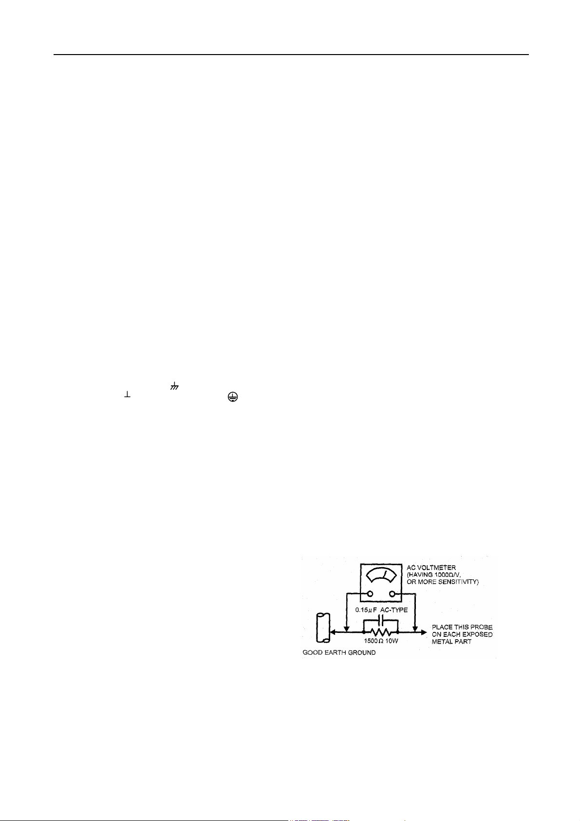
●Alternate Check Method
Plug the AC line cord directly into the AC outlet ( do not use a
line isolation transformer during this check.). Use an AC
voltmeter having 1000 ohms per volt or more sensitivity in the
following manner. Connect a 1500Ω 10W resistor paralleled
by a 0.15μF AC-type capacitor between an exposed metal
part and a known good earth ground (water pipe, etc.).
Measure the AC voltage across the resistor with the AC
voltmeter. Move the resistor connection to each exposed metal
part, particularly any exposed metal part having a return path
to the chassis, and measure the AC voltage across the resistor.
Now, reverse the plug in the AC outlet and repeat each
measurement. Any voltage measured must not exceed 0.75V
AC (r.m.s.). This corresponds to 0.5mA AC (r.m.s.).
However, in tropical area, this must not exceed 0.3V AC
(r.m.s.).
This corresponds to 0.2mA AC (r.m.s.)
3
Page 6
.
V
rCb
S
F
X
A
V
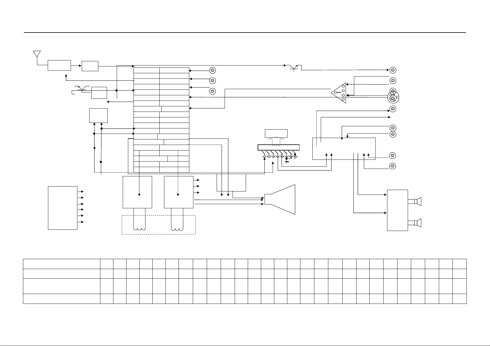
2. TV Block diagram
TUNER
SAW
S
TRAP
video
24C04
bus
POWER
UNIT
130V
24V
16V
8V
5V
3.3V
TDA8351
V OUT
PHILIPS UOC FUNCTIONAL DIFFERENCE BETWEEN THE VARIOUS IC VERSIONS
IC VERSION 9350 9351 9352 9353 9360 9361 9362 9363 9364 9365 9366 9367 9380 9381 9382 9383 9384 9385 9386 9387 9388 9389 9370 9373 9375 9377 9378
TV rang
Mono inter-carrier multi-standard
Sound demodulator (4.5-6.5MHz)
With switch able centre frequency
Audio switch
90 90 90 110 90 90 110 110 110 110 90 90 90 90 90 110 110 110 110 90 110 110 90 110 110 90 110
√ √ √ √ √ √ √ √ √ √ √ √ √ √ √ √ √
√ √ √ √ √ √ √ √ √ √ √ √ √ √ √ √ √
TDA93X
IF IN Y IN
RF AGC V IN
U IN
CVBSINT
CHROMA
IFVO OUT
CVBS/Y IN
SDA
SCL
AUDIO OUT IK
RGB OUT
V OUT H OUT
V IN
DY
H IN
H OUT
H OUT
bus
audio
video
TDA9874
7 4 5 1 2 6 7
CRT
XS303
8
5
video
audio
A OU TR
A OUTL
MAIN L
4052
audio
MAIN R
SDA/SCL
video
AV 1 L
audio
TDA9859
AV 2 L
AV 2 R
AV 2 R
M OUTR
M OUTL
Y
C
video
CRT PCB
200V
+15V
-15V
CREEN
OCUS
Y
C
Vi1
Vi2
V2i
V1i
ARo
ALo
ARi2
ARi1
ALi2
ALi1
N7522
OUT1-
OUT1+
OUT2-
OUT2+
o
S-VHS
4
Page 7

.
Automatic volume leveling
Automatic volume leveling or
Subcarrier output (for comb filter
applications)
QSS sound IF amplifier with
Separate input and AGC circuit
AM sound demodulator without
Extra reference circuit
PAL decoder
SECAM decoder
NTSC decoder
Horizontal geometry(E-W)
Horizontal and vertical zoom
ROM size
User RAM size
Tel e tex t
Closed captioning
√ √ √ √ √ √ √ √ √ √ √ √ √
√ √ √ √ √ √ √ √ √ √ √ √ √
√ √ √ √ √ √ √ √ √ √
√ √
√ √ √ √ √ √ √ √ √ √ √ √ √ √ √ √ √ √ √ √ √ √
√ √ √ √ √ √ √ √ √ √ √
√ √ √ √ √ √ √ √ √ √ √ √ √ √ √ √ √ √ √ √ √ √ √ √ √ √ √
√ √ √ √ √ √ √ √ √ √ √ √ √ √
√ √ √ √ √ √ √ √ √ √ √ √ √ √
32-
32-
32-
32-
64-
64-
64-
64-
64-
64-
64-
64-
16-
16-
16-
64k
64k
64k
64k
128
128
128
128
128
128
128
128
64k
64k
64k
1k 1k 1k 1k 2k 2k 2k 2k 2k 2k 2k 2k 1k 1k 1k 1k 1k 1k 1k 1k 1k 1k 2.25 2.25 2.25 2.25 2.25
1 p 1p 1p 1p 10p 10p 10p 10p 10p 10p 10p 10p
√ √ √ √ √ √ √ √ √ √ √ √ √ √ √ √ √ √ √ √ √ √ √ √ √ √ √
Block diagram TDA93xX PS/N2 series with mono intercarrier sound demodulator
1664k
1664k
1664k
1664k
1664k
1664k
1664k
3255k
3255k
3255k
3255k
3255k
5
Page 8
.
6
Page 9

3.REPLACEMENT OF MEMORY IC
1. MEMORY IC.
This TV uses memory IC. In the memory IC are memorized data for correctly operating the video and
deflection circuits.
When replacing memory IC, be sure to use IC written with the initial value of data.
2. PROCEDURE FOR REPLACING MEMORY IC
(1) Power off
Switch the power off and unplug the power cord from AC outlet.
(2) Replace IC
Be sure to use memory IC written with the initial data values.
(3) Power On
Plug the power cord into the AC outlet and switch the power On.
(4) Check and set SYSTEM default value:
1) Press “QV” key holding about 4 second and then press “MENU1” key on the Remote control unit.
Or Press “TEST” key on the Remote control unit for factory used.
2) The “TEST” will be displayed on the screen.
3) Press digital key, (Mkey) and corresponding on-screen display will be appeared.
Some time “PASSWORD” on-screen display will be appeared, you need to input 828.
4) Check the setting value of the SYSTEM default value of Table below. If the value is different, select
items by [CH+]/[CH-] keys and set value by [VOL+]/[VOL-] keys.
5) Press “STANDBY” key again and return to the normal screen.
4.SERVICE ADJUSTMENT
B1 POWER SUPPLY
1. Receive normal colour bar signal.
2. Connect DC voltmeter to VD541- and isolated ground.
3. Adjust potentiometer in power unit to get the voltage as 110V ±1.0V for 21 inch hereinafter,
130 ±1.0V for 25 inch upwards.
FOCUS ADJUSTMENT
1. Receive a crosshatch signal.
2. While watching the screen, adjust the FOCUS VR to make the vertical and horizontal lines as fine and
sharp as possible.
BUS CONTROL ADJUSTMENT
To enter BUS control mode, Press “TEST” key on the Remote control unit of factory.
Press “0” to “9“ key, (Mkey) and corresponding on-screen display will be appeared.
On TV screen “TEST” will be indicated, this means entered bus control mode.
And press following key, each function will be available.
Remote Hand Unit keys
[M1] [M2] [M3]
[M8] menu
c d e
f g h
i j k
[M0]
b
MENU8
V SLOPE
31
V SHIFT
31
7
V AMP
31
V SCOR
Page 10
MENU0 Geometrical adjustment
Receive PAL standard Complete pattern signal.
Adjustment steps:
a) Adjust V. SLOPE, to the center horizontal line just appeare from half bottom shadow.
b) Adjust V. SIZE, to get 90% of vertical picture contents would be displayed on CRT.
c) Adjust V. SHIFT, the center horizontal line correspond to CRT vertical center.
d) Adjust H.SHIFT, to get the picture horizontal center correspond to CRT horizontal center.
Receive NTSC signal and repeat above [M0] and [M1] adjustment.
[M7] Menu
AGC Adjustment.
Receive 60dBμ(1mV)V
colour bar pattern signal,adjust AGC value(voltage from high to low),to noise
H
reduce gradually and just disappeared point.
[M9] Menu
CRTcut off and white balance adjustment.
Receive white signal.
a) CRT cut off adjustment.
1. Select “SC”, then automatically vertical scan will be stopped.
2. Adjust SCREEN control on Flyback transformer to get the darkest single horizontal line (red,
green, or blue, sometimes shows more yellow, more purple or more white).
b) White balance adjustment.
1. Select RD/BD menu.
2. Adjust RD/BD to get colour temperature as x=281, y=311
c) Sub-Brightness adjustment. (Use stair case signal)
1. Select SB menu.
2. Adjust SB to get the darkest step being cutoff.
ICs Default Settings
1. TDA9381(1.0) EK cord=NTDA9381-----NG
MI Items Variable Preset MI Items Variable Preset
M0 AVL ON/OFF ON M4 SUBCON 0~63 63
FSL ON/OFF ON SUBCOL 0~63 63
FMWS ON/OFF OFF SUBSHP 0~63 63
FFI ON/OFF OFF SUBTINT 0~15 15
OSO ON/OFF ON YDLY PAL 0~15 12
FCO ON/OFF OFF YDLY NTSC 0~15 12
WOOFER ON/OFF OFF YDLY SEC 0~15 12
DUAL OUT 0~1 0 YDLY AV 0~15 12
Volume mode 0~1 1 UOC VOL ON/OFF Off
CATHODE 0~15 15
M1 BAND 0~2 2 SC BRI 0~63 10
AV CFG* 0~8 3
NTSC MX USA M5 OSD VPOS 0~63 53
VIDEO OUT CVBS OSD HPOS 0~59 15
PIN5 NTSC WIDE 0~63 15
PRO 0~3 0 ZOOM 0~63 59
NENU TITLE 0~6 3
M2 VISION IF 38.9M E2PROM ADRESS 0~33
DK ON/OFF OFF E2PROM VALUE 0~95
BG ON/OFF ON E2PROM WRITE
I ON/OFF OFF
M ON/OFF OFF M8 FREQUENCY 50HZ 60HZ
SIF PREFER BG VSLOPE 0~63 31 31
AUTO SOUND ON/OFF ON VSHIFT 0~63 31 31
VAMP 0~63 31 31
M3 START ON 0~2 0 VSCOR 0~63 31 31
ENGLISH ON/OFF ON HSHIFT 0~63 31 31
8
Page 11
ARABIC ON/OFF OFF
PERSIAN ON/OFF OFF M9 BT 0~63 48
TURKISH ON/OFF OFF CT 0~63 48
FRANCE ON/OFF OFF SC OFF
RUSSIA ON/OFF OFF RB 0~63 32
GB 0~63 32
M6 SHIPMODE RD 0~63 32
SEARCH SPEED 0~3 0 GD 0~63 32
M7 AGC-TOP 0~63 25 BD 0~63 32
AGC-SPEED 0~3 2 SB 0~63 40
2. TDA9361(1.1) EK cord=NTDA9361-----NF
MI Items Variable Preset MI Items Variable Preset
M0 AVL ON/OFF ON M4 SUBCON 0~63 63
FSL ON/OFF ON SUBCOL 0~63 63
FMWS ON/OFF OFF SUBSHP 0~63 63
FFI ON/OFF OFF SUBTINT 0~15 15
OSO ON/OFF ON YDLY PAL 0~15 12
FCO ON/OFF OFF YDLY NTSC 0~15 12
WOOFER ON/OFF OFF YDLY SEC 0~15 12
DUAL OUT 0~1 0 YDLY AV 0~15 12
Volume mode 0~1 1 UOC VOL ON/OFF Off
CATHODE 0~15 15
M1 BAND 0~2 2 SC BRI 0~63 10
AV CFG* 0~8 3
NTSC MX USA M6 LOGO ON/OFF ON
VIDEO OUT CVBS LOGO COLUR 0~7 0
PIN5 NTSC LOGO POSITION 0~11 0
PRO 0~3 0 LOGO CHAR
SHIPMODE
M2 VISION IF 38.9M SEARCH SPEED 0~3 0
DK ON/OFF OFF
BG ON/OFF ON M7 AGC-TOP 0~63 25
I ON/OFF OFF AGC-SPEED 0~3 2
M ON/OFF OFF
SIF PREFER BG M8 FREQUENCY 50HZ 60HZ
AUTO SOUND ON/OFF ON VSLOPE 0~63 31 31
VSHIFT 0~63 31 31
M3 START ON 0~2 0 VAMP 0~63 31 31
ENGLISH ON/OFF ON VSCOR 0~63 31 31
ARABIC ON/OFF OFF HSHIFT 0~63 31 31
PERSIAN ON/OFF OFF
TURKISH ON/OFF OFF M9 BT 0~63 48
FRANCE ON/OFF OFF CT 0~63 48
RUSSIA ON/OFF OFF SC OFF
Spanish bit 0~1 0 RB 0~63 32
TXT DEF 0~3 0 GB 0~63 32
RD 0~63 32
M5 OSD VPOS 0~63 53 GD 0~63 32
OSD HPOS 0~59 15 BD 0~63 32
WIDE 0~63 15 SB 0~63 40
ZOOM 0~63 59
NENU TITLE 0~6 3
9
Page 12

5. ICs functional description
UOC TDA93XX
SYMBOL PIN DESCRIPTION
STAND BY output. 1 In STAND BY mode, high level (Power OFF).
For Power ON this pin will be reduced to low.
SCL 2 I2C-bus clock line
SDA 3 I2C-bus data line
TUNING 4 tuning Voltage (Vt) PWM output
P3.0/NTSC SW 5 Port 3.0 or NTSC output/SCART SW input, Forced NTSC selection,
Low-level output, otherwise High output.
KEY 6 Control keys input *3
VOL 7 Sound Volume control PWM output
MUTE 8 Sound mute output
VSSC/P 9 Digit ground for µ-controller core and periphery
BAND1 10 Tuner Band selection output
BAND2 11 Tuner Band selection output
VSSA 12 Analog ground of teletext decoder and digital ground of TV-processor
SECPLL 13 SECAM PLL decoupling
VP2 14 2nd supply voltage TV-processor(+8V)
DECDIG 15 decoupling digital supply of TV-processor
PH2LF 16 Phase-2 filter
PH1LF 17 Phase-1 filter
GND3 18 Ground 3 for TV-processor
DECBG 19 Band gap decoupling
AVL/EWD 20 Automatic volume leveling /EAST-WEST drive output
VDRB 21 Vertical drive B output
VDRA 22 Vertical drive A output
IFIN1 23 IF input 1
IFIN2 24 IF input 2
IREF 25 Reference current input
VSC 26 Vertical sawtooth capacitor
TUNER AGC 27 T uner AGC output
AUDEEM/SIFIN1 *1 28 Audio deemphasis or SIF input
DECSDEM/SIFIN2 29
GND2 30
SNDPLL/SIFAGC *1 31
AVL/SNDIF/REF0/
32
AMOUT *1
HOUT 33
FBISO 34
AUDEXT/QSSO/
35
AMOUT *1
EHTO 36
PLL IF 37
IFVO/SVO 38
VP1 39
CVBS INT 40
GND1 41
CVBS/Y 42
CHROMA 43
AUDOUT/AMOUT *1
44
INSSW2 45
R2/VIN 46
decoupling sound demodulator or SIF input 2
ground 2 for TV processor
narrow band PLL filter or AGC sound IF
Automatic Volume Levelling / sound IF input / subcarrier reference output / audio
deemphasis
horizontal output
flyback input/sandcastle output
external audio output / QSS intercarrier out
EHT/overvoltage protection input
IF-PLL loop filter
IF video output / selected CVBS output
supply voltage TV processor
internal CVBS input
ground for TV processor
CVBS/Y input
C input
audio output /AM audio output (volume controlled)
2nd RGB / YUV insertion input
2nd R input / V (R-Y) input / PR input
10
Page 13
G2/YIN 47
B2/UIN 48
BCLIN 49
BLKIN 50
RO 51
GO 52
BO 53
VDDA 54
VPE 55
VDDC 56
OSCGND 57
XTALIN 58
XTALOUT 59
RESET 60
VDDP 61
P1.0/INT1 62
P1.1/T0 63
P1.2/INT0 64
Note
1. The function of pin 20, 28, 29, 31, 32, 35 and 44 is dependent on the IC version (mono intercarrier FM demodulator /QSS IF
amplifier and East-West output or not) and on some software control bits. The valid combinations are given in table 1.
2. the vertical guard function can be controlled via pin 49 or pin 50. the selection is made by means of the
IVG bit in subaddress 2BH.
2nd G input / Y input
2nd B input / U (B-Y) input / PB input
beam current limiter input
black current input / V-guard input
Red output
Green output
Blue output
analog supply of Closed Caption decoder and digital supply of TV-processor (3.3 V)
OTP Programming Voltage
digital supply to core (3.3 V)
oscillator ground supply
crystal oscillator input
crystal oscillator output
reset
digital supply to periphery (+3.3 V)
TV/AV (AV1) / AV2 /S-VHS mode Output.
TV/AV (AV1) / AV2 /S-VHS mode Output.
Remote control signal input.
TABLE 1
IC version FM-PLL version QSS version
East-West Y/N N Y N Y
CMB1/CMB0
bits
AM bits
Pin 20
Pin 28 AUDEEM SIFIN1
Pin 29 DECSDEM SIFIN2
Pin 31 SNDPLL SIFAGC
Pin 32
Pin 35
Pin 44 AUDOUT Controlled AM or audio out
Note
1. When additional (external) selectivity is required for FM-PLL system pin 32 can be used as sound IF input. This function is
selected by means of SIF bit in subaddress 28H.
00 01/10/11 00 01/10/11 00 01/10/11 00 01/10/11
- - - - - 0 1 - 0 1
AVL EWD AVL EWD
SNDIF(1) REFO(2) AVL/SNDIF(1) REFO(2) AMOUT REFO(2) AMOUT REFO(2)
AUDEXT AUDEXT QSSO AMOUT AUDEXT QSSO AMOUT
2. the reference output signal is only available for the CMB1/CMB0 setting of 0/1. for the other settings this pin is a switch
output(see also 5 table 67).
Pin No. 6: Control keys input (Max. Limit voltage)
Function POWER MENU TV/AV V- V+ P- P+
Voltage 0 0.4125 0.825 1.2375 1.65 2.0625 2.475
AN7522/7523 Function : audio output
Symbol PIN Function Symbol PIN Function
Vcc 1 Power supply GND 7 ground
Out 1 (+) 2 Ch 1 output (+) In 2 8 Ch 2 input
GND(out 1) 3 Ch 1Ground VOL 9 Volume Control
Out 1 (-) 4 Ch 1 output (-) Out 2 (-) 10 Ch 2 output (-)
Standby 5 Mute input GND(out 2) 11 Ch 2 Ground
In 1 6 Ch 1 input Out 2 (+) 12 Ch 2 output (+)
Note: AN7523 is pin 1 to 9, AN7522 is pin 1 to 12.
11
Page 14
pp
LA78040/78045 Function : vertical output
Symbol PIN Function Symbol PIN Function
INV IN 1 Input V OUT 5 Vertical output
VCC1 2 Power VCC2 6 Output power supply
PUMP UP 3 Pump up power NON INV IN 7 Negative feedback
GND 4 Ground
TDA9859 Function : Universal Sound processor
Symbol Pin Function Symbol Pin Function
AV1L 1 AV1 Audio Left input AV1R 32 AV1 Audio input Right
P1 2 Not used P2 31 Not used
MAINL 3 Main Audio Left input AV2R 30 AV2 Audio input Right
CSMO 4 Smoothing Capacitor CPS1 29 Pseudo stereo Cap. 1
MAINR 5 Main Audio Right input AV2L 28 AV2 Audio input Left
VP 6 Power Supply CPS2 27 Pseudo stereo Cap. 2
OUT R 7 Right Output OUT L 26 Left Output
GND 8 Ground MAD 25 Not used (GND)
LINOR 9 Line Output Right LINOL 24 Line Output Left
LINIR 10 Line Input Right LINIL 23 Line Input Left
CBR1 11 Bass Cap. Right 1 CBL1 22 Bass Cap. Left 1
CBR2 12 Bass Cap. Right 2 CBL2 21 Bass Cap. Left 2
Headphone R 13 Headphone-R output Headphone L 20 Headphone-L output
CTR 14 Treble Cap. Right CTL 19 Treble Cap. Left
MAINOR 15 Main Audio out Right MAINOL 18 Main Audio out Left
SCL 16 I2C Bus clock SDA 17 I2C Bus data
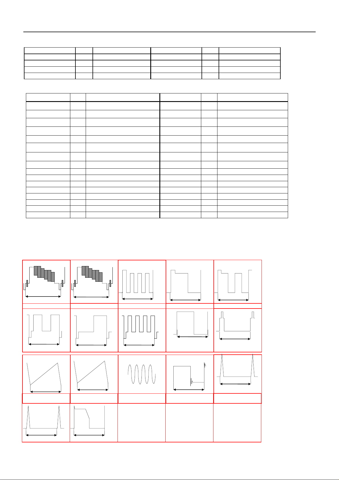
6. Test point Waveforms
2.6Vpp
H
TDA93XX
95Vpp
PIN38
H
1Vpp
TDA93XX
PIN21
V
22Vpp
H H
HEATER
1.2Vpp
H
TDA93XX
95Vpp
PIN40
H H
CRT KG CRT KR
0.8Vpp
TDA93XX
PIN22
V
300Vpp
T511 PIN7
3.8Vpp
TDA93XX
95Vpp
PIN53
CRT KB
1.3V
TDA93XX
PIN59
H
2.5Vpp
H H
TDA93XX
0.9Vpp
PIN52
H
TDA93XX
PIN33
2.7Vpp
H
V451 B
12
2.5Vpp
TDA93XX
5Vpp
PIN51
TDA93XX
PIN34
H
1000Vpp
H
V451 C
Page 15
7. IC voltages
TDA93XX
PIN 1 2 3 4 5 6 7 8 9 10 11 12 13 14 15 16
V 2.8 3.8 3.6 3.3 3.5 3.5 0.1 0.1 0 5.4 0.1 0 2.3 8 5 3
PIN 17 18 19 20 21 22 23 24 25 26 27 28 29 30 31 32
V 4 0 4 0.9 0.7 0.8 1.9 1.9 3.9 3.8 1.6 3.2 3.4 0 2.4 0.1
PIN 33 34 35 36 37 38 39 40 41 42 43 44 45 46 47 48
V 0.6 0.5 3.7 1.7 2.4 3.1 8 3.8 0 3.4 1.5 3.6 2.3 2.6 2.6 2.6
PIN 49 50 51 52 53 54 55 56 57 58 59 60 61 62 63 64
V 2.3 7.2 2.7 2.7 2.7 3.5 0 3.5 0.1 1.7 1.8 0 3.5 0.1 0.1 5
LA76040
PIN 1 2 3 4 5 6 7
V 0.7 15 -12 -15 0.3 15.9 -0.07
AN 7522
PIN 1 2 3 4 5 6 7 8 9 10 11 12
V 12 7 0 7 3.3 1.4 0 1.4 0 7 0 7
TDA9859
PIN 1 2 3 4 5 6 7 8 9 10 11 12 13 14
V 4.0 0 4.0 8.0 4.0 8.0 4.0 0 4.0 4.0 4.0 4.0 4.0 4.0
PIN 15 16 17 18 19 20 21 22 23 24 25 26 27 28
V 4.0 4.5 4.6 4.0 4.0 4.0 4.0 4.0 4.0 4.0 0 4.0 4.0 4.0
PIN 29 30 31 32
V 4.0 4.0 0 4.0
13
Page 16
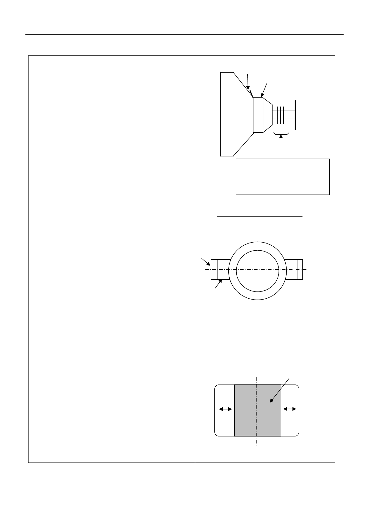
8. PURITY / CONVERGENCE ADJUSTMENT
PURITY ADJUSTMENT
1. Demagnetize CRT with the demagnetizer.
2. Loosen the retainer screw of the deflection yoke.
3.
Remove the wedges.
4.
Input a green raster signal from the signal generator,
and turn the screen to green raster.
5.
Move the deflection yoke backward.
6.
Bring the long lug of the purity magnets on the short
lug and position them horizontally. (Fig2)
7.
Adjust the gap between two lugs so that the GREEN
RASTER will come into the center of the screen. (Fig.
3)
8.
Move the deflection yoke forward, and fix the position
of the deflection yoke so that the whole screen will
become green.
9.
Insert the wedge to the top side of the deflection yoke
so that it will not move.
10.
Imput a crosshatch signal.
11.
Verify that the screen is horizontal.
12.
Input red and blue raster signals, and make sure that
purity is properly adjusted.
Long lug
Short lug
WEDGE
DEFLECTION
YOKE
P
CRT
P: PURITY MAGNET
4: 4-POLES
6: 6-POLES (convergence magnets)
4 6
P/C MAGNETS
(convergence magnets)
Fig. 1
PURITY MAGNETS
Bring the long lug over the short lug
and position them horizontally.
Fig. 2
(FRONT VIEW)
GREEN RASTER
CENTER
Fig. 3
14
Page 17
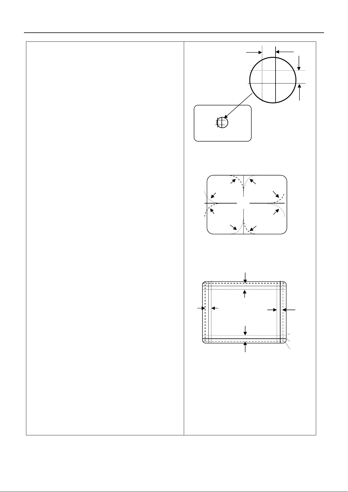
STATIC CONVERGENCE ADJUSTMENT
1. Input a crosshatch signal.
2. Using 4-pole convergence magnets, overlap the red and
blue lines in the center of the screen (Fig. 1) and turn
them to magenta (red/blue).
3. Using 6-pole convergence magnets, overlap the magenta
(red/blue) and green lines in the center of the screen and
turn them to white.
4. Repeat 2 and 3 above, and make the best convergence.
DYNAMIC CONVERGENCE ADJUSTMENT
1. Move the deflection yoke up and down and overlap lines
in the periphery. (Fig. 2)
2. Move the deflection yoke left to right and overlap the
lines in the periphery. (Fig. 3)
3. Repeat 1 and 2 above, and make the best convergence.
After adjustment, fix the wedge at the original position.
Fasten the retainer screw of the deflection yoke.
Fix the 6 magnets with glue.
(FRONT VIEW)
Fig. 1
(FRONT VIEW)
RED GREEN BLUE
BLUE
RED
GREEN
GREEN
RED
BLUE
BLUE GREEN RED
Fig.2
(FRONT VIEW)
RED GREEN BLUE BLUE
GREEN RED
RED
GREEN
BLUE
BLUE
GREEN
RED
Fig. 3
15
Page 18

9. List of Parts
NAME TYPE Q'TY REMARK
CU-2988(AUSTRALIA)
PC BOARD MODULE
CRT BOARD MODULE
KEY AND REMOTE CONTROL BOARD MODULE
PRINTED CIRCUIT BOARD
TOUCH SWITCH KFC-A06-21050 1
TOUCH SWITCH KFC-A06-21050 1
TOUCH SWITCH KFC-A06-21050 1
TOUCH SWITCH KFC-A06-21050 1
TOUCH SWITCH KFC-A06-21050 1
TOUCH SWITCH KFC-A06-21050 1
CARBON FILM RESISTOR
CARBON FILM RESISTOR
CARBON FILM RESISTOR
CARBON FILM RESISTOR
CARBON FILM RESISTOR
CARBON FILM RESISTOR
LED BT205-L 1
INRARED RECEIVER HS0038A IMPORTATION 1
WIRE WIRE
FRONT AV MODULE
PRINTED CIRCUIT BOARD
AV SOCKET AV3-8.35-6AK 1
WIRE WIRE
FRONT FRAME MODULE
FRONT FRAME ASSEMBLY
FRONT FRAME (ABS)
LIGHT CONDUCTION COLUMN
BOLT SJ2825-87 ST3X8F 1
FUNCTION KEY MTAH4055AA--Q 1
BOLT SJ2825-87 ST3X8F 2
POWER BUTTON
SPRING MTBH4090BC--Q 1
CRT TRESTLE
CRT BRACKET
BOLT SJ2824-87 ST4X16F 20
SPEAKER
BOLT SJ2824-87 ST4X12F 8
METAL SCUTCHEON Haier 49mm ARGENTINE 1
WIRE WIRE 1
BACK COVER MODULE
BACK COVER ASSEMBLY
BACK COVER
RT13-1/6W-470Ω-J-T52
RT13-1/6W-560Ω-J-T52
RT13-1/6W-1KΩ-J-T52
RT13-1/6W-1.2KΩ-J-T52
RT13-1/6W-1.8KΩ-J-T52
RT13-1/6W-390Ω-J-T52
FRONT AV BOARD
BJK4076-----Q 1
MTAA4086AA--Q 1
MTAA4098AA--Q 1
MTAH4057AA--Q 1
MTAH4056AA--Q 1
MTAH4058AA--Q 2
4
YDT0813-10W-8Ω-01 2
BJH4075-----Q 1
MTAA4078AB--Q 1
MTAA4092AB--Q 1
1
1
1
1
1
1
1
1
1
1
1
16
Page 19

INTEGER MATERIEL MODULE
RUBBER TRAY H=3mm 4
DEGUASSING COIL TIE MTAJ1001AG--Q 4
NUT M6 ASSEMBLED NUT 4
101 HIGHVOLTAGE CLAMP TEM101 1
411 CLAMPER MTAJ3000AA--Q 2
POWER BUTTON CLAMPER
TERMINAL BOARD MTAH4059AC--Q
POTHOOK MTAH4059AA--Q 1
BOLT SJ2824-87 ST4X12F 2
BOLT
BOLT
BOLT
PAD (TOP)
PAD (BO T TOM)
WIRE 60mm 1
CRT M68LWF188X50 1
DEGUASSING COIL
GROUNDING WIRE 1
GAUCHE CONNECTING WIRE 1
BRACKET MODULE
BRACKET
BOLT
FBT TRANSFORMER TRESTLE
BOLT SJ2824-87 ST4X12F 2
POWER CABLE PRE-WORKING MODULE
POWER BUTTON CAP
POWER CABLE
POWER SWITCH
POWER TRANSMITTING WIRE
PACKING ARK MODULE 1
POWER CABLE PLASTIC BAG
WIRE
OPERATION INTRODUCTIONS(ENGLISH)
TEAC PROPAGANDIZE PAGE 1
POP STATIC FILM (ENGLISH)
BATTERY
REMOTE CONTROL
OPERATION INTRODUCTIONS PLASTIC BAG
29“90 SERIES INTEGER PLASTIC BAG 1
PACKI N G A RK 1
ENCASEMENT NAIL 20
BACK COVER LABEL
TRANSPORT SCUTCHEON 2
BJZ4078-----Q
MTAH4060AA--Q
SJ2825-87 ST3X12F 2
SJ2824-87 ST4X16F 10
SJ2824-87 ST4X16F 6
MTEA4058----Q
MTEA4059----Q
1
BXY4069-----Q
MTAC4068AA--Q
SJ2825-87 ST3X10F
MTAC4072AC--Q
MTAB0014AA--Q 1
1
1
1
1
60mm 1
1
1
5# 2
1
1
1
1
1
1
1
1
1
1
17
Page 20

Mainboard element list
r01n r14 r02 ra
TF-0090----1J 1 T451
RCD152K-NACNH 3 1/2W 1.5K R918 R928 R938
RDB100J-NAATD 3 1/6W 10 R312 R801 R871
R301 R302 R363 R365 R366 R381
RDB101J-NAATD 8 1/6W 100
8
2 R861 R862
RDB102J-NAATD 8 1/6W 1K
8
2 R825 R827
RDB103J-NAATD 8 1/6W 10K
8
8
RDB104J-NAATD 5 1/6W 100K R441 R444 R483 R802AR803A
RDB122J-NAATD 3 1/6W 1.2K R305 R560 R713
RDB151J-NAATD 3 1/6W 150 R815AR848 R852
RDB152J-NAATD 2 1/6W 1.5K R397 R732
RDB153J-NAATD 1 1/6W 15K R331
RDB154J-NAATD 1 1/6W 150K R318
RDB181J-NAATD 1 1/6W 180 R353
RDB182J-NAATD 3 1/6W 1.8K R403 R405 R714
RDB183J-NAATD 1 1/6W 18K R162
RDB220J-NAATD 3 1/6W 22 R914 R924 R934
RDB221J-NAATD 5 1/6W 220 R311 R442 R917 R927 R937
RDB222J-NAATD 6 1/6W 2.2K R351 R371 R451 R540 R701AR804
RDB223J-NAATD 2 1/6W 22K R384 R455
RDB242J-NAATD 1 1/6W 2.4K R515
RDB272J-NAATD 2 1/6W 2.7K R321 R512
RDB273J-NAATD 2 1/6W 27K R484 R487
RDB274J-NAATD 1 1/6W 270K R174
RDB301J-NAATD 3 1/6W 300 R913 R923 R933
RDB330J-NAATD 2 1/6W 33 R398 R806
RDB331J-NAATD 3 1/6W 330 R916 R926 R936
RDB332J-NAATD 8 1/6W 3.3K
1 R742
RDB333J-NAATD 5 1/6W 33K R171 R175 R317 R385 R434
RDB391J-NAATD 2 1/6W 390 R322 R775
RDB392J-NAATD 1 1/6W 3.9K R462
RDB470J-NAATD 5 1/6W 47 R368 R708 R911 R921 R931
RDB471J-NAATD 2 1/6W 470 R308 R710
RDB472J-NAATD 7 1/6W 4.7K
R382 R383
R401 R402 R452 R723 R724 R743
R815 R824
R128 R129 R369 R460 R464 R481
R531 R541
R544 R712 R734 R802 R803 R807
R816 R818
R126 R127 R163 R380 R395 R396
R461 R543
R548 R551 R704 R705 R706 R707
R709 R816A
R818AR825AR827AR851AR852AR912
R922 R932
R702 R721 R722 R728 R735 R736
R737 R741
R131 R133 R154 R158 R306 R443
R733
18
Page 21

RDB473J-NAATD 3 1/6W 47K R172 R732AR745
RDB560J-NAATD 2 1/6W 56 R354 R355
RDB561J-NAATD 1 1/6W 560 R711
RDB562J-NAATD 2 1/6W 5.6K R370 R701
RDB564J-NAATD 1 1/6W 560K R465
RDB680J-NAATD 1 1/6W 68 R304
RDB681J-NAATD 3 1/6W 680 R316 R463 R482
RDB683J-NAATD 1 1/6W 68K R173
RDB750J-NAATD 1 1/6W 75 R805
RDB820J-NAATD 1 1/6W 82 R313
RDB822J-NAATD 3 1/6W 8.2K R153AR157AR562
RDC101J-NABTD 1 1/4W 100 R486
RDC103J-NABTD 1 1/4W 10K R485
RDC1R0J-NABTD 1 1/4W 1.0 R404
RDC222J-NABTD 1 1/4W 2.2K R161
RDC270J-NABTD 1 1/4W 27 R561
RDC2R7J-NABTD 1 1/4W 2.7 R468
RDC334J-NABTD 1 1/4W 330K R942
RDC513J-NABTD 2 1/4W 51K R539 R539A
RDC8R2J-NABTD 1 1/4W 8.2 R513
RDD102J-NACTD 1 1/2W 1K R453
RDD683J-NACTD 2 1/2W 68K R507 R508
RFD1R0J4ACCNF 1 1/2W 1.0 R473B
RFER27J5ACDNF 3 1W 0.27 R555 R565 R566
RFER47J5ACDNF 3 1W 0.47 R165 R470 R472
RGDX246K-03NZ 1 1/2W 24M R519
RJB393F-NAATD 1 1/6W 39K R411
RSE102J4ACCND 1 1W 1K R466
RSE1R5J4DCCND 1 1W 1.5 R406
RSE1R8J4DCCND 1 1W 1.8 R408
RSE220J5ACCND 1 1W 22 R300A
RSF101J5ACDND 1 2W 100 R407
RSF103J5ACDND 5 2W 10K R467 R703 R915 R925 R935
RSF223J7ACDND 1 2W 22K R556
RSF271J7ACDND 2 2W 270 R454 R546
RSF2R0J7ACDND 1 2W 2.0 R480
RSF2R2J5ACDND 1 2W 2.2 R445
RSF560J5ACDND 1 2W 56 R530
RSF5R6J5ACDND 1 2W 5.6 R941
RSG473J7ACEND 1 3W 47K R504
RWH3R9K4AK-NS 1 5W 3.9 R458
VDAAA203A001C 1 20KB VR501
CCF121J1CA-FC 2 50V120P C701 C701A
CCF330J1CA-FC 2 50V33P C761 C762
C308 C311 C340 C401 C402 C481
CKF102K1BA-FC 8 50V1000P
C721 C861
C162 C302 C309 C312 C313 C332
CKF103Z1FA-FC 8 50V0.01u
C362 C472
C475 C535 C703AC723 C744 C752
7
C756
CKF222K1BA-FC 1 50V2200P C335
CKF331K1BA-FC 3 50V330P C911 C921 C931
19
Page 22

C445 C513 C732 C803 C805 C812
CKF471K1BA-FC 8 50V470P
C814 C824
1 C826
CKF472K1BA-FC 2 50V4700P C324 C336
CKF561K1BA-FC 1 50V560P C381
CKF821K1BA-FC 1 50V820P C323
CKMX102M301ND 1 AC400V1000P C515
CKMX471K301ND 2 AC400V470P C515AC598
CKP101K1BA-FC 1 500V100P C482
CKP102K1BA-FC 1 500V1000P C452
CKP221K1BA-NC 1 500V220P C405
CKP392K1BA-FC 1 500V3900P C451
CKW102K2BJ-ND 4 1KV1000P C503 C504 C505 C506
CKW471K2RA-ND 2 1KV470P C523 C529
CKX102P2EJ-ND 2 2KV1000P C512 C943
CKX221K2RA-ND 1 2KV220P C509
CKX471K2RA-ND 2 2KV470P C521 C543
CKX681K2RA-ND 1 2KV680P C527
CEB101MYACBNP 1 10V100u C548
C163AC172 C301 C307 C322 C363
CEC100MYACANP 8 16V10u
C364 C367
4 C751 C807 C841 C871
CEC101MYACBNP 2 16V100u C361 C743
CEC220MYACANP 1 16V22u C745
C116 C171 C333 C352 C561
CEC470MYACANP 8 16V47u
C723AC811 C823
CEC471MYACCNP 3 16V470u C525 C532 C801
CED101MYACBNP 5 25V100u C406 C471 C471AC474 C474A
CED102M1ACHNP 1 25V1000u C522
CED222M2ACKNP 1 25V2200u C524
CED471M1ACENP 1 25V470u C161
CEE331M1ACFNP 1 35V330u C530
CEE470MYACCNP 1 35V47u C453
C153 C157 C163 C337 C804 C806
CEF1R0MYACANP 8 50V1u
C813 C815
3 C825 C827 C862
CEF220MYACBNP 1 50V22u C703
CEF2R2MYACANP 2 50V2.2u C339 C755
CEF470MYACBNP 2 50V47u C462 C517
CEF4R7MYACANP 4 50V4.7u C303 C304 C325 C464
CEFR47MYACANP 4 50V0.47u C121 C123 C372 C374
CEH100M1ACENP 1 160V10u C458
CEH471M3AEBNK 1 160V470u C528B
CEH4R7MYBCCNP 1 160V4.7u C466
CEK100M1ACHNP 2 250V10u C477 C941
CEM331M3AEMNC 1 400V330u(30*40) C507
CPFX6R8MY01NP 1 50V6.8u(Non-polarity) C446
CAY104K1-H-FC 5 63V0.1u C326 C338 C365 C411 C511
CAY224K1-H-FC 2 63V0.22u C331 C334
CAY474K1-H-FD 2 63V-0.47u K C404 C461
CFG104K2-H-NW 4 100V0.1u C460 C705 C706 C707
CFG332K1-H-NW 1 100V3300P C321
20
Page 23

CFG333K1-H-NW 3 100V0.033u C403 C510 C544
CFG473K1-H-NW 1 100V0.047u C443
CFG562J1-H-NW 2 100V5600P C154 C158
CMLX224M901NE 1 AC300V0.22u M C501
CMM434J8-H-NL 1 400V0.43u C467
CMR103J5-H-NE 1 630V0.01u C508
CMZ822J7-H-NE 1 1.6KV8200p C455
CMZ912J7-H-NE 1 1.6KV9100P C456
LAD601K2---NJ 1 LGB-600uH(1.5A) L441
LBB100K----TG 5 10uH-K L331 L361 L751 L752 L753
LBB1R0K----TG 1 1uH-K L302
LBB220K----TG 1 22uH-K L401
LBB3R9K----TG 1 3.9uH-K L351
LBB820K----TG 3 82uH-K L911 L912 L913
LEA001-5---NJ 2 M-COIL L450 L505
LEE004-----NJ 2 6*5*1.5mm ZD524AZD524B
LF-013-3---NJ 1 LINE COIL L452
LG-013-----NL 1 LINE FILTER10*12.5 L501
DH2120M001-NC 1 PTC12ohm PS501
DN14R7M001-NC 1 NTC4.7ohm R502
DLC42001---NA 1 FG314002E(LED) VD775
VD171 VD461 VD462 VD482 VD511 VD544
DR1N4148---TH 8 1N4148
VD561 VD562
4 VD734 VD911 VD921 VD931
DRBAV21----NJ 3 BAV21 VD912 VD922 VD932
DRGP15M----ND 4 GP15M VD503 VD504 VD505 VD506
VD401 VD470 VD471 VD510 VD512 VD522
DRRGP10D---TD 7 RGP10D
VD525
DRRGP10J---TD 3 RGP10J VD436 VD472 VD513
DRRGP15D---ND 1 RGP15D VD543
DRRGP30D---ND 1 RGP30D VD521
DRRGP30J---ND 1 RGP30J VD524
DRTRU4C----NZ 1 TRU4C VD452
DRTRU4DS---NZ 1 TRU4DS VD451
DRTVR4J----NL 1 TVR4J VD508
DZHZ22-2---TL 1 HZ22-2 VD481
DZHZ3C3----TL 1 HZ3C3 VD564
DZHZ4A2----TL 1 HZ4A2 VD509
DZHZ5C1----TL 1 HZ5C1 VD300A
DZHZ7C1----TL 3 HZ7C1 VD381 VD382 VD383
DZHZ9A3----TL 5 HZ9A3 VD460 VD483 VD822 VD941 VD861A
NAN7522N---N- 1 AN7522N N161
NAT138A----N- 1 AT138A U 701
NAT24C08---N- 1 AT24C08 N702
NCW574CS---N- 1 CW574CS N703
NHEF4052---BP 2 HEF4052 N121 N801
NKA431AZ---F- 1 KA431AZ V540
NKA5Q1265RFN- 1 KA5Q1265RF N501
NLTV817B---N- 1 LTV817B N504
NMC7805CT--N- 1 MC7805CT N505
NMC7808CT--N- 1 MC7808CT N503
NTDA8177---N- 1 TDA8177 N401
21
Page 24

NTDA9373---N- 1 TDA9373 N301
Q2PA1015-GNF- 1 2PA1015G V171
V121 V122 V173 V351 V352 V395
Q2PC1815-GNF- 8 2PC1815 G
V504 V801
Q2SB1443--NN- 1 2SB1443 TV2 Q V542
Q2SD1886C-NN- 1 2SD1886C V451
QBF421----NN- 3 BF421 V913 V923 V933
QBF422----NN- 3 BF422 V912 V922 V932
QIRFS630A-NN- 1 IRFS630A V432
QKSC1674C-NN- 1 KSC1674C V308
QKSC2383-ONN- 1 KSC2383O V450
QKSC2688--NN- 3 KSC2688 V911 V921 V931
QPH2369---NN- 1 PH2369 V701
FBA3154S02C-A 1 FUSE 3.15A250V F501
KPW12HL002--D 1 POWERSWITCH(A20) K 501
KTA11HA090--Y 6 PUSH SWITCH(10.85mm) SW701 SW702 SW703 SW704 SW705 SW706
XFS043-----NB 1 SAW FILTER(K2966M D2901C Z301
XTC008-----ND 1 T5.5M Z354
XX-021-----NV 1 CR.OSC(12M 18P) X761
GAAV2001----Y 2 2S SOCKET XR502 XS501
GABV2001----A 1 2S SOCKET XS904
GABV2001----N 1 2S SOCKET XS502
GABV5001----A 1 DY SOCKET DYa XS403
GACV4001----A 1 4S SOCKET XS161
GAGBD001----- 1 ICSOCKET1.78mm 64P XS1
GBAVL007----A 1 CRTSOCKET XS901
GBBA3-05----Y 1 AVSOCKET XS803
GBBB9-03----Y 1 AVSOCKET(AV9-8.4-04) XS801
GBCH5001----Y 1 S SOCKET XS861
JW4451-J001-A 1 4P LINE(450mm D2-D2) XP402
JW5431-J132-A 1 5P LINE(E3D 430mm) XS903
TD-0042----0L 1 H-DRIVERBCH-13 T450
TM-0097----0N 1 CON.TRANS T501
BXATB066----X 1 TUNER(5V38.9) A101
M90X0003---91 1 INSULATED MAT18*13 D4.8 Z1
MB0X0011---G8 2 FUSE SOCKET F501AF501B
MB1X0040---BF 1 12VRADIATOR H-N505
MB1X0101---BF 1 POWERRADIATOR(2SC4237) H-N501
MB1X0113---BF 1 VOCALITY RADIATOR H-N161
MB1X0114---BF 1 5VRADIATOR(CUBA) H-N503
MB1X0163---BG 1 RADIATOR(NIGRESCENCE) H-V432
MB1X0208---BF 1 H-RADIATOR H-V451
MG3X0036---D7 1 INSULATED WASHER(D9) Z2
MG3X0037---D7 1 INSULATED WASHER(D9) Z3
zz120 zz121 zz122 zz124 zz125 zz126
MN0X0004---G8 8 D1.6*3.0 RIVET
zz127 zz128
zz129 zz130 zz131 zz132 zz133 zz134
7
zz135
zz108 zz109 zz110 zz111 zz112 zz113
MN0X0005---G8 8 D2.5*3.5 RIVET
zz114 zz115
zz116 zz117 zz118 zz119 zz143 zz148
8
zz149 zz150
22
Page 25

1 zz152
PX20028----2C 1 MAIN+CRTPCB zz060
SCA-25012FE-H 1 GB818 M2.5*12 SN401
SFAC30010FE1H 3 SJ2836-87(M3*10.I) SN503 SN161ASN161B
SFAC30012FE1H 2 SJ2836-87(M3*12.I) S-N501 S-V451
SKA-308R0FE-H 2 GB845-78 ST3*8 S-N505 S-V432
SXN1A25--FF-H 1 M2.5 NUT zz360
SXN1A30--FF-H 5 M3(NUT) N-N501 N-N503 N-V451 NN161ANN161B
SXW1A25--FE-H 1 GB97.1 D2.5 FLATWASHIER ZN401
23
Page 26
1110987654321
R217
R218
15K
470
V202
V201
BF422
V205
BF423
R222
R221
10
10K
R225
D208
C206
470
IN4148
270P
R211 1K
R232
R201
C214
C214
0.1u/500V
R228
10K
I+1I-2Vp3VOB4Gnd5VFB6VOA7Vguard8VIFB
100uF/25V
C302
10n
C418
390n/400V
+16V-1
+45V
330uF/35V
4.7u/500V
D211
IN4148
C305
C417
C2688/BF422
V231
R229
10K
TDA8356/8351
+
Gnd
+B
Gnd
+
N301
R303
100K
220K
Gnd
+
C306
22uF/50V
33/0.5W
270pF/500V
R416
100
100uF/63V
+24V
R236
10
C207
270P
R307
2
C416
15K
R309 2.7
L401
AC41A
C426
R412
5.6
7
C409
10uF/160V
D407
BYD33J
+
Gnd
R237
47
R235
470
V207
BF422
V208
BF423
1
1
R308
1.2
R415
1K
+
C427
1uF/160V
Gnd
BYV95B
D406
BYD33G
C412
470pF/500V
+
C415
22uF/250V
C2688/BF422
R238
10K
IN4148
R231
470
9
Gnd
+35V
1
L405
6.8mH
+
D405
Gnd
+24V
47uF/50V
R402
100
6
5
4
3
2
1
1
2
3
4
BZX79C8V2
C405
123
ZD405
R?R219
47
R220
10K
+16V-1
GND GND
Gnd
R401
R426
3.9K
1
4.7K
4
C620
0.022uF
R615
Gnd
15K
R201 470
R306
2.2/1W
R302
C301
10n
C2688/BF422
R227
47
3K
13
SW707
KEY
U101
D
+8V
X001
Video1
C
B
A
Audio1-L
Audio1-R
Video2
Audio2-L
Audio2-R
Video-Out
Audio-Out-L
Audio-Out-R
X005
S-VHS
Gnd
1
o
2
t
XP802
RT801
CON2
MZ73-18
C801
0.1uF/275VAC
220VAC
1 2 3 4 5 6 7 8 9 10 11 12
ENV59D68F1E
AGC1VT2Hi/n.c.3Mi/BS1(SCL)4Lo/BS2(SDA)5V+6i.c.(V+)7i.c.8i.c.(+33V)9IFGND10IF
N807
7805
In Out
Gnd
Gnd
R102
R529
27K
6.8K
C102
10nF
+
+
R103
100K
C105
C101
Gnd
4.7uF/16V
4.7uF/16V
R001
82
C005
100nF
R003
47K
C006
R002
100nF
47K
R004
82
C003
R006
100nF
47K
C004
100nF
R005
47K
Gnd
R021
220
R022
220
R01982R020
82
R015
Gnd
1K
R016
1K
TVR4N
C807
1000pF/1KV
C802
0.1uF/275VAC
C806
1000pF/1KV
R802
L801
LCLI-5
SW801
KDC-A10
5W/1.8
1
R801
F801
220K
3.15A/250VAC
D801
7
C106
4.7uF/16V
10uF/16V
10uF/16V
D805
TVR4N
D802
TVR4N
+
C011
C012
10uF/16V
+
+
TVR4N
R805
5.6K
1000pF/1KV
D806
10uF/16V
C007
+
Gnd
C108
+
C107
4.7uF/16V
AV1
+
C808
1000pF/1KV
V801
2SB892
Gnd
Stand-by
AV2
1
2
3
4
5
6
7
8 9
Gnd
1
2
3
4
5
6
7
8
Gnd
LCLI-5
C809
KEY
Vol.+ AV/TVVol.- MenuProg. -Prog.+
R724
R725
1.2K
1.8K
11
C109
10nF
N001
HEF4053
1
0
1
1
0
0
N002
HEF4052
Vdd
0
1
2
0
3
1
2
3
E
A0
Vee
A1
2 TO 4
Decoder
Vss
L802
C811
+
150uF/400V
D807
1N4148
D808
1N4004
D809
1N4148
R807
680
KEY
C110
10nF
10uF/16V
1
4
R723
1K
R105
4.7K
R107
2.2K
16
15
14
13
12
11
10
16
15
14
C008
13
+
12
11
10
9
23
N801
PC817B
C815
100nF
R817
22K
KEY
KEY
KEY
GndGndGndGndGndGnd
R721
R722
470
620
+8V
R121
10
L102
C112
R110
1uH
10nF
330
Gnd
Z101
C116
S2950
10nF
1
10
V101
2
BF370
Gnd
3
R109
22
Gnd
R108
82
Gnd
+5V
R007 10
C001
+
10uF/16V
Gnd
R712
3.3K
+5V
R008
10
+
Gnd
R011
C002
220K
10uF/16V
Gnd
R014
C010
10
470uF/16V
+
XS603
CON3
R808
R812
5
120K
68
R809
120K
C816
680pF/2KV
R810
R811
V802
15K
39
C4237
2
R815
22
R816
1.8K
12M/RS11
V805
2SC3807
C819
15nF
1000pF/400VAC
C818
12nF
R714
R010
220K
V002
BC548
R013
1K
+3.3V
R726
3.3K
R727
R756
47
4.7K
4
5
8
R114
12K
R772
ZD702
15K
uPC574
+
C704
Gnd
10uF/50V
R775
R771
10K
10K
C731
100nF
C730
100nF
Gnd
R113
3.3K
V102
BC548
R112
47K
Gnd
AV1
AV2
FM
3.3K
+8V
R009
C009
10
10uF/16V
+
Gnd
V001
BC548
R012
1K
Gnd
123
T801
3
7
1
2
R819
C820
GND
C821
470pF/1KV
1
2
+8V
3
XP560
4
CON6
5
6
C822
220uF/160V
R821
D811
+
2
12K
MYV28-600
Gnd
D812
BYM26B
13
12
9
14
15
10
16
11
R829
2.7K
C825
470pF/500V
+
C826
220uF/35V
C837
D815
BYM26B
470uF/25V
C836
470pF/500V
Gnd
D816
BYV28-600
C832
Gnd
470pF/500V
+
C835
470uF/25V
Gnd
+
+B
+8V
D882(P)
2
R770
12K
PH2369
V807
Gnd
V701
R111
47K
Stand-by
R822
100K
Gnd
D882(P)
R728
3.3K
V808
BC548
V809
1
2
3
4
+5V-1
WP
Vdd
n.c.
PTC
A2
SCL
Vss
SDA
N702
24C08
C701
10uF/16V
+
+
Gnd
Gnd
C736
10uF/16V
R729
3.3K
TO 0'
Vol1
Vol2
Vol1
Vol2
C530
22nF
FM
SC
+8V
R506
47
R826 47K
ZD802
R825
BZX79C6V8
150K
V806
BC548
RP801
R828
2K
4.7K
R830
10K
R837
2.2K
C848
22uF/25V
Gnd
C847
+
100uF/16V
Gnd Gnd
R845470
8
7
6
5
O
Gnd
Gnd
+
100uF/16V
Gnd
Gnd
R757
100
C728
10nF
R755
100
+
R838
N806
7808
In Out
C845
+8V
ZD501
8.2V
R741
100
R530
C532
C510
47uF/16V
2
100
R841
560
Gnd
Gnd
Gnd
R753
100
R718
5.6K
R782
5.6K
L505
10uH
100uF/16V
C529
3300pF
R827
22K
Gnd
+
Gnd
R716
3.3K
C512
C907
1uF/63V
C536
4700
39K
100nF
ZD806
BZX79C2V4
+
Gnd
+8V
C515
100nF
+
Gnd
R305 100
R301 100
R525 3.9K
Gnd
R503
2.2K
R840
1K
V840
C1815
C846
100uF/16V
ZD807
BZX79C5V1
R777
27K
R717
3.3K
C514
1000pF
BC548
+130V
+24V
C908
4700pF
+
Gnd
C520
1200p
V505
R936
390
+
Gnd
+5V-1
R758
R759
3.3K
R705
27K
R701
1K
R780 2.2K
R781 2.2K
Gnd
C909
220nF
C918
2200pF
100nF
C508
+
C509 2.2uF/16V
C513
1000pF
R907
820K
C522
330p
C518
220nF
R910
15K
C528
10uF/16V
Gnd
+
Gnd
+
C923
2.2uF/50V
3.3K
1
2
3
4
5
6
7
8
9
10
11
12
13
14
15
16
17
18
19
20
21
22
23
24
25
26
27
28
29
30
31
32
C727
56pF
R750
3.3K
Standby
SCL
SDA
Tuning
System
Key
Vol.1
Vol.2
Vss C/P
Band1
Band2
VssA
SECPLL
Vp2
DECDIG
PH2LF
PH1LF
Gnd3
DECBG
AVL/EWD
VDRB
VDRA
IF1
IF2
IREF
VSC
Tuner AGC
AUDEEM/SIF1
DECSDEM/SIF2
Gnd2
SNDPLL/SIFAGC
AVL/REFO
C726
56pF
Gnd
+3.3V
N501
TDA9373
64
IRin
63
AV2
62
AV1
61
VddP
60
Reset
Z701
59
XTALout
58
XTALin
12MHz
57
OscGnd
56
VddC
55
VpE
Gnd
54
VddA
53
Bout
R903
52
Gout
R904
51
Rout
R901 10K
50
Blanking
49
BCLin
48
B2/Uin
47
G2/Yin
46
R2/Vin
45
INSSW2
44
AUDOUT/AMOUT
43
CHROMA
42
CVBS/Y
41
Gnd1
Gnd
40
CVBSINT
39
Vp1
38
IFVO/SVO
37
PLLIF
36
EHTO
35
AUDEXT/QSSO
34
FBISO
Gnd
33
H. out
C538
R534
+8V
1000p
1.8K
R915 27K
V501
L502
R510
6.8uH
1.8K
R519
330
R522
V502
47
R511
BC548
330
Gnd
Gnd
R537
470
Illustration:
1. The unit of all resistors is . K=1000, M=1,000,000
2. The power of all unmarked resistors is 1/6W.
3. The unit of capacitors is F commonly. "p" represents for pF. If there is no additional
illustration, the working voltage of capacitors is 63V.
4. This diagram only illustrates the basic and typical model. Exceptional parts or part circuits may
be different from the fact circuit.
Note:
1. As the parts marked with are relevant to the whole-set's safety, the replaced ones must be the
same with Service Manual.
2.The circuit enclosed by = = is connected to the AC power directly. While repairing, the service
man should connect a buffer transformer between TV and AC power to avoid electrical shock.
Gnd
Gnd
+
C527
47uF/16V
D601
1N4148
R607
10K
R525
470
R536
+8V
47
Gnd
C612
+
100uF/16V
V601
Gnd
BC558
R608
47K
Gnd
Gnd
V841
C1815
C888
470uF/10V
+8V
BC548
R538
180
Gnd
+16V
R521
47
Z507
XT5.5
Z508
XT-6.5
R535
56K
+
C507
1uF/16V
+3.3V
R732
470
D701
LED
CP701
HS0038
+5V-1
123
+
C732
47uF/16V
R766
Gnd
100
C708
2.2uF/16V
C702
C703
R902
100
C901
100nF
C902
C903
100nF
C517 10uF/16V
+
C511
100nF
C519
R502
390
Gnd
V602
BC548
+17V
R620
1.8K
+
33p
33p
L702 10uH
100
100nF
Gnd
Gnd
L703
+3.3V
C706
10uH
100nF
C705
+
100uF/16V
ZD906
BZX79C8V2
Gnd
100
ZD905
BZX79C8V2
100nF
R920
82
1000pF
R92182R922
R533
1K
Gnd
C505
100nF
+8V
R531
100K
R532
27K
N602
TDA7057AQ
Vol.11n.c.2Input(1)3Vp4Input(2)5SGND6Vol.27Output2(+)8PGND29Output2(-)10Output1(-)11PGND12Output1(+)
C615
0.022uF
R611
C625
15K
10nF
Gnd
Gnd
C616
22nF
C626
470nF
R621
6.8K
Gnd
XP603
CON2
0.22/1W
1
2
R610
Only For Reference
L701
10uH
C707
+ C516
+3.3V
+3.3V
82
+
Gnd
C912
100uF/16V
1uF/16V
+
1000uF/25V
Gnd
R628
1.8K
25"29"34" TDA9373 Narrow Power Voltage Circuit Diagram
XS201
CON6
XS202
CON5
R905
+8V
XP201
33K
CON5
1
2
3
4
5
ZD907
R906
BZX79C8V2
22K
Gnd
Gnd
XP902
1
2
CON4
3
4
R923
1K
Gnd
L901
+8V
10uH
C915
22nF
220pF/500V
Gnd Gnd Gnd
C622
10nF
XP601
Gnd
CON4
C617
C621
470nF
V605
R612
BC548
47K
R629
6.8K
Gnd
SW702
SW703
SW704
SW705
SW706
V211
R238
10K
D216
R312
22K
Gnd
Gnd
+
100uF/35V
R407
C401
R246
R210
470
15K
V210
BF422
V210
BF423
R240
10
R241
C208
470
270P
1
R310
330
2
1
6
8
5
4
3
9
T402
FBT
C309
220nF/100V
+8V
10
11
12
13
7
R205 1.5K
Gnd
BZX79C15V
R425
5.1K*
C420
100nF
R204
1.5K
KB
KG
KR
R206
1.5K
1
R311
Gnd
22
D408
R417
1N4148
680
R418
1K
ZD401
R427
1.5/2W
EHT
Focus
G2
R422
1K
D411
1N4148
Gnd
C450
C477
2200pF
TO O
O'
2
C402
270
470pF/500V
+
Gnd
R408
2.2K
C403
V401
3900pF
2SC2383O
Gnd
Gnd
T401
BCT-25-1K1
Gnd
BU2508DX/
BU2720DX
R410
82
Gnd
Gnd
XP205
G1 G2 G3
S-Gnd
R419
56K
D410
1N4148
R421
10K
R476
680
V452
BC548
V402
EHT
S-Gnd
R430
1.8K
Gnd
R480
R496
68K
R208
1.5K
C203
1000pF/2KV
C425
+
10uF/25V
6.8K
8n2/2KV
Gnd
V456
BC558
1N4148
Gnd
C406
33n/400V
D450
C413
XP204
1
CON1
XP402
CON5
R481
12K
R455
2.7K
5
4
3
2
1
Gnd
C407
8n2/2KV
Gnd
12
V
H
XP202
4
3
2
1
CON4
Gnd
R456
1W/6.8
1
C458
6.8uF/100V
V457
D2012
Gnd
D412
BY228
D415
BYW95C
D
C
B
+
Gnd
L402
600uH
A
Page 27
UOC TDA9373 SERIES
L
A
U
N
S
S
S
E
E
M
M
E
R
E
R
E
COLOUR TELEVISION
V
V
I
I
C
C
E
C
I
V
R
M
A
A
A
N
N
U
U
A
A
L
L
PUSH PUSH
CT-M6845
Page 28

.
CONTENTS
1. safety precautions…………………………………………………………………………..……………3
2. TV block diagram
and PHILIPS UOC functional difference between the various IC versions …………….…..…….4
3. Replacement of memory IC………………………………………………………… …………………7
4. Service adjustment………………………………………………………… ………………………...7
5. ICs functional description………………………………………………………………………………9
6. Test point waveform………………………………………………………………………………….…12
7. All ICs/transistors voltages…………………………………………………………………………….13
8. Purity / convergence adjustment……………………………………………………………………..14
9. List of Parts ………………………………………………………………………….………………….16
2
Page 29

.
1.SAFETY PRECAUTIONS
1. The design of this product contains special hardware, many
circuits and components specially for safety purposes. For
continued protection, no changes should be made to the
original design unless authorized in writing by the
manufacturer. Replacement parts must be identical to those
used in the original circuits. Service should be performed by
qualified personnel only.
2. Alterations of the design or circuitry of the products should
not be made. Any design alterations or additions will void the
manufacturer’s warranty and will further relieve the
manufacturer of responsibility for personal injury or property
damage resulting therefrom.
3. Many electrical and mechanical parts in the products have
special safety-related characteristics. These characteristics are
often not evident from visual inspection nor can the protection
afforded by them necessarily be obtained by using
replacement components rated for higher voltage, wattage, etc.
Replacement parts which have these special safety
characteristics are identified in the parts list of Service
manual. Electrical components having such features are identified
by shading on the schematics and by ( ! ) on the parts list in
Service manual. The use of a substitute replacement which does
not have the same safety characteristics as the recommended
replacement part shown in the parts list of Service manual
may cause shock, fire, or other hazards
4. Don’t short between the LIVE side ground and ISOLATED
(NEUTRAL) side ground or EARTH side ground when repairing.
Some model’s power circuit is partly different in the GND.
The difference of the GND is shown by the LIVE: ( ) sid e
GND, ISOLATED (NEUTRAL) : ( ) side GND and
EARTH : ( ) side GND. Don’t short between the LIVE
side GND and ISOLATED (NEUTRAL) side GND or EARTH
side GND and never measure with a measuring apparatus
(oscilloscope etc.) the LIVE side GND and ISOLATED
(NEUTRAL) side GND or EARTH side GND at the same time.
If above note will not be kept, a fuse or any parts will be
broken.
5. If any repair has been made to the chassis, it is recommended
that the B1 setting should be checked or adjusted (See
ADJUSTMENT OF B1 POWER SUPPLY).
6. The high voltage applied to the picture tube must conform
with that specified in Service manual. Excessive high voltage
can cause an increase in X-Ray emission, arcing and possible
component damage, therefore operation under excessive high
voltage conditions should be kept to a minimum, or should be
prevented. If severe arcing occurs, remove the AC power
immediately and determine the cause by visual inspection
(incorrect installation, cracked or melted high voltage harness,
poor soldering, etc.). To maintain the proper minimum level of
soft X-Ray emission, components in the high voltage circuitry
including the picture tube must be the exact replacements or
alternatives approved by the manufacturer of the complete
product.
7. Do not check high voltage by drawing an arc. Use a high
voltage meter or a high voltage probe with a VTVM.
Discharge the picture tube before attempting meter
connection, by connecting a clip lead to the ground frame and
connecting the other end of the lead through a 10kΩ 2W
resitor to the anode button.
8. When service is required, observe the original lead dress.
Extra precaution should be given to assure correct lead dress
in the high voltage circuit area. Where a short circuit has
occurred, those components that indicate evidence of
overheating should be replaced. Always use the
9. manufacturer’s replacement components.
10. Isolation Check
(Safety for Electrical Shock Hazard)
After re-assembling the product, always perform an isolation
check on the exposed metal parts of the cabinet (antenna
terminals, video/audio input and output terminals, Control
knobs, metal cabinet, screwheads, earphone jack, control
shafts, etc.) to be sure the product is safe to operate without
danger of electrical shock.
11. The surface of the TV screen is coated with a thin film which
can easily be damaged. Be very careful with it when handle the
TV. Should the TV screen become soiled, wipe it with a soft
dry cloth. Never rub it forcefully. Never use any cleaner or
detergent on it.
(1) Dielectric Strength Test
The isolation between the AC primary circuit and all metal
parts exposed to the user, particularly any exposed metal part
having a return path to the chassis should withstand a voltage
of 3000V AC (r.m.s.) for a period of one second.
(…Withstand a voltage of 1100V AC (r.m.s.) to an appliance
rated up to 120V, and 3000V AC (r.m.s.) to an appliance rated
200V or more, for a periode of one second.)
This method of test requires a test equipment not generally
found in the service trade.
(2) Leakage Current Check
Plug the AC line cord directly into the AC outlet (do not use a
line isolation transformer during this check.). Using a
“Leakage Current Tester”, measure the leakage current from
each exposed metal part of the cabinet, particularly any
exposed metal part having a return path to the chassis, to a
known good earth ground (water pipe, etc.). Any leakage
current must not exceed 0.5mA AC (r.m.s.).
However, in tropical area, this must not exceed 0.2mA AC
(r.m.s.).
●Alternate Check Method
Plug the AC line cord directly into the AC outlet ( do not use a
line isolation transformer during this check.). Use an AC
voltmeter having 1000 ohms per volt or more sensitivity in the
following manner. Connect a 1500Ω 10W resistor paralleled
by a 0.15μF AC-type capacitor between an exposed metal part
and a known good earth ground (water pipe, etc.). Measure
the AC voltage across the resistor with the AC voltmeter. Move
the resistor connection to each exposed metal part,
particularly any exposed metal part having a return path to
the chassis, and measure the AC voltage across the resistor.
Now, reverse the plug in the AC outlet and repeat each
measurement. Any voltage measured must not exceed 0.75V
AC (r.m.s.). This corresponds to 0.5mA AC (r.m.s.).
However, in tropical area, this must not exceed 0.3V AC
(r.m.s.).
This corresponds to 0.2mA AC (r.m.s.)
3
Page 30

.
V
rCb
S
F
X
A
R
R
V
2. TV Block diagram
TUNER
SAW
S
TRAP
video
24C04
bus
POWER
UNIT
130V
24V
16V
8V
5V
3.3V
TDA8351
V OUT
PHILIPS UOC FUNCTIONAL DIFFERENCE BETWEEN THE VARIOUS IC VERSIONS
IC VERSION 9350 9351 9352 9353 9360 9361 9362 9363 9364 9365 9366 9367 9380 9381 9382 9383 9384 9385 9386 9387 9388 9389 9370 9373 9375 9377 9378
TV rang
Mono inter-carrier multi-standard
Sound demodulator (4.5-6.5MHz)
With switch able centre frequency
Audio switch
90 90 90 110 90 90 110 110 110 110 90 90 90 90 90 110 110 110 110 90 110 110 90 110 110 90 110
√ √ √ √ √ √ √ √ √ √ √ √ √ √ √ √ √
√ √ √ √ √ √ √ √ √ √ √ √ √ √ √ √ √
TDA93X
video
200V
+15V
-15V
Y
C
CRT PCB
CREEN
OCUS
IF IN Y IN
RF AGC V IN
U IN
CVBSINT
CHROMA
IFVO OUT
CVBS/Y IN
SDA
SCL
AUDIO OUT IK
RGB OUT
V OUT H OUT
V IN
DY
H IN
H OUT
H OUT
bus
audio
video
TDA9874
7 4 5 1 2 6 7
CRT
XS303
8
5
video
audio
A OU T
A OU TL
MAIN L
4052
audio
MAIN R
SDA/SCL
AV 2 RAV 2
o
Y
C
N7522
Vi1
OUT1-
Vi2
OUT2-
V2i
V1i
ARo
S-VHS
ALo
ARi2
ARi1
ALi2
ALi1
OUT1+
OUT2+
video
TDA9859
M OUTR
M OUTL
AV 1 L
AV 2 L
audio
4
Page 31

.
Automatic volume leveling
Automatic volume leveling or
Subcarrier output (for comb filter
applications)
QSS sound IF amplifier with
Separate input and AGC circuit
AM sound demodulator without
Extra reference circuit
PAL decoder
SECAM decoder
NTSC decoder
Horizontal geometry(E-W)
Horizontal and vertical zoom
ROM size
User RAM size
Tel e tex t
Closed captioning
√ √ √ √ √ √ √ √ √ √ √ √ √
√ √ √ √ √ √ √ √ √ √ √ √ √
√ √ √ √ √ √ √ √ √ √
√ √
√ √ √ √ √ √ √ √ √ √ √ √ √ √ √ √ √ √ √ √ √ √
√ √ √ √ √ √ √ √ √ √ √
√ √ √ √ √ √ √ √ √ √ √ √ √ √ √ √ √ √ √ √ √ √ √ √ √ √ √
√ √ √ √ √ √ √ √ √ √ √ √ √ √
√ √ √ √ √ √ √ √ √ √ √ √ √ √
32-
32-
32-
32-
64-
64-
64-
64-
64-
64-
64-
64-
16-
16-
16-
64k
64k
64k
64k
128
128
128
128
128
128
128
128
64k
64k
64k
1k 1k 1k 1k 2k 2k 2k 2k 2k 2k 2k 2k 1k 1k 1k 1k 1k 1k 1k 1k 1k 1k 2.25 2.25 2.25 2.25 2.25
1 p 1p 1p 1p 10p 10p 10p 10p 10p 10p 10p 10p
√ √ √ √ √ √ √ √ √ √ √ √ √ √ √ √ √ √ √ √ √ √ √ √ √ √ √
Block diagram TDA93xX PS/N2 series with mono intercarrier sound demodulator
1664k
1664k
1664k
1664k
1664k
1664k
1664k
3255k
3255k
3255k
3255k
3255k
5
Page 32

.
6
Page 33

3.REPLACEMENT OF MEMORY IC
1. MEMORY IC.
This TV uses memory IC. In the memory IC are memorized data for correctly operating the video and
deflection circuits.
When replacing memory IC, be sure to use IC written with the initial value of data.
2. PROCEDURE FOR REPLACING MEMORY IC
(1) Power off
Switch the power off and unplug the power cord from AC outlet.
(2) Replace IC
Be sure to use memory IC written with the initial data values.
(3) Power On
Plug the power cord into the AC outlet and switch the power On.
(4) Check and set SYSTEM default value:
1) Press “QV” key holding about 4 second and then press “MENU1” key on the Remote control unit.
Or Press “TEST” key on the Remote control unit for factory used.
2) The “TEST” will be displayed on the screen.
3) Press digital key, (Mkey) and corresponding on-screen display will be appeared.
Some time “PASSWORD” on-screen display will be appeared, you need to input 828.
4) Check the setting value of the SYSTEM default value of Table below. If the value is different, select
items by [CH+]/[CH-] keys and set value by [VOL+]/[VOL-] keys.
5) Press “STANDBY” key again and return to the normal screen.
4.SERVICE ADJUSTMENT
B1 POWER SUPPLY
1. Receive normal colour bar signal.
2. Connect DC voltmeter to VD541- and isolated ground.
3. Adjust potentiometer in power unit to get the voltage as 110V ±1.0V for 21 inch hereinafter,
130 ±1.0V for 25 inch upwards.
FOCUS ADJUSTMENT
1. Receive a crosshatch signal.
2. While watching the screen, adjust the FOCUS VR to make the vertical and horizontal lines as fine and
sharp as possible.
BUS CONTROL ADJUSTMENT
To enter BUS control mode, Press “TEST” key on the Remote control unit of factory.
Press “0” to “9“ key, (Mkey) and corresponding on-screen display will be appeared.
On TV screen “TEST” will be indicated, this means entered bus control mode.
And press following key, each function will be available.
Remote Hand Unit keys
[M1] [M2] [M3]
[M8] menu
c d e
f g h
i j k
[M0]
b
MENU8
V SLOPE
31
V SHIFT
31
7
V AMP
31
V SCOR
Page 34

MENU0 Geometrical adjustment
Receive PAL standard Complete pattern signal.
Adjustment steps:
a) Adjust V. SLOPE, to the center horizontal line just appeare from half bottom shadow.
b) Adjust V. SIZE, to get 90% of vertical picture contents would be displayed on CRT.
c) Adjust V. SHIFT, the center horizontal line correspond to CRT vertical center.
d) Adjust H.SHIFT, to get the picture horizontal center correspond to CRT horizontal center.
Receive NTSC signal and repeat above [M0] and [M1] adjustment.
[M7] Menu
AGC Adjustment.
Receive 60dBμ(1mV)V
colour bar pattern signal,adjust AGC value(voltage from high to low),to noise
H
reduce gradually and just disappeared point.
[M9] Menu
CRTcut off and white balance adjustment.
Receive white signal.
a) CRT cut off adjustment.
1. Select “SC”, then automatically vertical scan will be stopped.
2. Adjust SCREEN control on Flyback transformer to get the darkest single horizontal line (red,
green, or blue, sometimes shows more yellow, more purple or more white).
b) White balance adjustment.
1. Select RD/BD menu.
2. Adjust RD/BD to get colour temperature as x=281, y=311
c) Sub-Brightness adjustment. (Use stair case signal)
1. Select SB menu.
2. Adjust SB to get the darkest step being cutoff.
ICs Default Settings
1. TDA9381(1.0) EK cord=NTDA9381-----NG
MI Items Variable Preset MI Items Variable Preset
M0 AVL ON/OFF ON M4 SUBCON 0~63 63
FSL ON/OFF ON SUBCOL 0~63 63
FMWS ON/OFF OFF SUBSHP 0~63 63
FFI ON/OFF OFF SUBTINT 0~15 15
OSO ON/OFF ON YDLY PAL 0~15 12
FCO ON/OFF OFF YDLY NTSC 0~15 12
WOOFER ON/OFF OFF YDLY SEC 0~15 12
DUAL OUT 0~1 0 YDLY AV 0~15 12
Volume mode 0~1 1 UOC VOL ON/OFF Off
CATHODE 0~15 15
M1 BAND 0~2 2 SC BRI 0~63 10
AV CFG* 0~8 3
NTSC MX USA M5 OSD VPOS 0~63 53
VIDEO OUT CVBS OSD HPOS 0~59 15
PIN5 NTSC WIDE 0~63 15
PRO 0~3 0 ZOOM 0~63 59
NENU TITLE 0~6 3
M2 VISION IF 38.9M E2PROM ADRESS 0~33
DK ON/OFF OFF E2PROM VALUE 0~95
BG ON/OFF ON E2PROM WRITE
I ON/OFF OFF
M ON/OFF OFF M8 FREQUENCY 50HZ 60HZ
SIF PREFER BG VSLOPE 0~63 31 31
AUTO SOUND ON/OFF ON VSHIFT 0~63 31 31
VAMP 0~63 31 31
M3 START ON 0~2 0 VSCOR 0~63 31 31
8
Page 35

ENGLISH ON/OFF ON HSHIFT 0~63 31 31
ARABIC ON/OFF OFF
PERSIAN ON/OFF OFF M9 BT 0~63 48
TURKISH ON/OFF OFF CT 0~63 48
FRANCE ON/OFF OFF SC OFF
RUSSIA ON/OFF OFF RB 0~63 32
GB 0~63 32
M6 SHIPMODE RD 0~63 32
SEARCH SPEED 0~3 0 GD 0~63 32
M7 AGC-TOP 0~63 25 BD 0~63 32
AGC-SPEED 0~3 2 SB 0~63 40
2. TDA9361(1.1) EK cord=NTDA9361-----NF
MI Items Variable Preset MI Items Variable Preset
M0 AVL ON/OFF ON M4 SUBCON 0~63 63
FSL ON/OFF ON SUBCOL 0~63 63
FMWS ON/OFF OFF SUBSHP 0~63 63
FFI ON/OFF OFF SUBTINT 0~15 15
OSO ON/OFF ON YDLY PAL 0~15 12
FCO ON/OFF OFF YDLY NTSC 0~15 12
WOOFER ON/OFF OFF YDLY SEC 0~15 12
DUAL OUT 0~1 0 YDLY AV 0~15 12
Volume mode 0~1 1 UOC VOL ON/OFF Off
CATHODE 0~15 15
M1 BAND 0~2 2 SC BRI 0~63 10
AV CFG* 0~8 3
NTSC MX USA M6 LOGO ON/OFF ON
VIDEO OUT CVBS LOGO COLUR 0~7 0
PIN5 NTSC LOGO POSITION 0~11 0
PRO 0~3 0 LOGO CHAR
SHIPMODE
M2 VISION IF 38.9M SEARCH SPEED 0~3 0
DK ON/OFF OFF
BG ON/OFF ON M7 AGC-TOP 0~63 25
I ON/OFF OFF AGC-SPEED 0~3 2
M ON/OFF OFF
SIF PREFER BG M8 FREQUENCY 50HZ 60HZ
AUTO SOUND ON/OFF ON VSLOPE 0~63 31 31
VSHIFT 0~63 31 31
M3 START ON 0~2 0 VAMP 0~63 31 31
ENGLISH ON/OFF ON VSCOR 0~63 31 31
ARABIC ON/OFF OFF HSHIFT 0~63 31 31
PERSIAN ON/OFF OFF
TURKISH ON/OFF OFF M9 BT 0~63 48
FRANCE ON/OFF OFF CT 0~63 48
RUSSIA ON/OFF OFF SC OFF
Spanish bit 0~1 0 RB 0~63 32
TXT DEF 0~3 0 GB 0~63 32
RD 0~63 32
M5 OSD VPOS 0~63 53 GD 0~63 32
OSD HPOS 0~59 15 BD 0~63 32
WIDE 0~63 15 SB 0~63 40
ZOOM 0~63 59
NENU TITLE 0~6 3
9
Page 36

5. ICs functional description
UOC TDA93XX
SYMBOL PIN DESCRIPTION
STAND BY output. 1 In STAND BY mode, high level (Power OFF).
For Power ON this pin will be reduced to low.
SCL 2 I2C-bus clock line
SDA 3 I2C-bus data line
TUNING 4 tuning Voltage (Vt) PWM output
P3.0/NTSC SW 5 Port 3.0 or NTSC output/SCART SW input, Forced NTSC selection,
Low-level output, otherwise High output.
KEY 6 Control keys input *3
VOL 7 Sound Volume control PWM output
MUTE 8 Sound mute output
VSSC/P 9 Digit ground for µ-controller core and periphery
BAND1 10 Tuner Band selection output
BAND2 11 Tuner Band selection output
VSSA 12 Analog ground of teletext decoder and digital ground of TV-processor
SECPLL 13 SECAM PLL decoupling
VP2 14 2nd supply voltage TV-processor(+8V)
DECDIG 15 decoupling digital supply of TV-processor
PH2LF 16 Phase-2 filter
PH1LF 17 Phase-1 filter
GND3 18 Ground 3 for TV-processor
DECBG 19 Band gap decoupling
AVL/EWD 20 Automatic volume leveling /EAST-WEST drive output
VDRB 21 Vertical drive B output
VDRA 22 Vertical drive A output
IFIN1 23 IF input 1
IFIN2 24 IF input 2
IREF 25 Reference current input
VSC 26 Vertical sawtooth capacitor
TUNER AGC 27 T uner AGC output
AUDEEM/SIFIN1 *1 28 Audio deemphasis or SIF input
DECSDEM/SIFIN2 29
GND2 30
SNDPLL/SIFAGC *1 31
AVL/SNDIF/REF0/
32
AMOUT *1
HOUT 33
FBISO 34
AUDEXT/QSSO/
35
AMOUT *1
EHTO 36
PLL IF 37
IFVO/SVO 38
VP1 39
CVBS INT 40
GND1 41
CVBS/Y 42
CHROMA 43
AUDOUT/AMOUT *1
44
decoupling sound demodulator or SIF input 2
ground 2 for TV processor
narrow band PLL filter or AGC sound IF
Automatic Volume Levelling / sound IF input / subcarrier reference output / audio
deemphasis
horizontal output
flyback input/sandcastle output
external audio output / QSS intercarrier out
EHT/overvoltage protection input
IF-PLL loop filter
IF video output / selected CVBS output
supply voltage TV processor
internal CVBS input
ground for TV processor
CVBS/Y input
C input
audio output /AM audio output (volume controlled)
10
Page 37

INSSW2 45
R2/VIN 46
G2/YIN 47
B2/UIN 48
BCLIN 49
BLKIN 50
RO 51
GO 52
BO 53
VDDA 54
VPE 55
VDDC 56
OSCGND 57
XTALIN 58
XTALOUT 59
RESET 60
VDDP 61
P1.0/INT1 62
P1.1/T0 63
P1.2/INT0 64
Note
1. The function of pin 20, 28, 29, 31, 32, 35 and 44 is dependent on the IC version (mono intercarrier FM demodulator /QSS IF
amplifier and East-West output or not) and on some software control bits. The valid combinations are given in table 1.
2. the vertical guard function can be controlled via pin 49 or pin 50. the selection is made by means of the
IVG bit in subaddress 2BH.
2nd RGB / YUV insertion input
2nd R input / V (R-Y) input / PR input
2nd G input / Y input
2nd B input / U (B-Y) input / PB input
beam current limiter input
black current input / V-guard input
Red output
Green output
Blue output
analog supply of Closed Caption decoder and digital supply of TV-processor (3.3 V)
OTP Programming Voltage
digital supply to core (3.3 V)
oscillator ground supply
crystal oscillator input
crystal oscillator output
reset
digital supply to periphery (+3.3 V)
TV/AV (AV1) / AV2 /S-VHS mode Output.
TV/AV (AV1) / AV2 /S-VHS mode Output.
Remote control signal input.
TABLE 1
IC version FM-PLL version QSS version
East-West Y/N N Y N Y
CMB1/CMB0
bits
AM bits
Pin 20
Pin 28 AUDEEM SIFIN1
Pin 29 DECSDEM SIFIN2
Pin 31 SNDPLL SIFAGC
Pin 32
Pin 35
Pin 44 AUDOUT Controlled AM or audio out
Note
1. When additional (external) selectivity is required for FM-PLL system pin 32 can be used as sound IF input. This function is
selected by means of SIF bit in subaddress 28H.
00 01/10/11 00 01/10/11 00 01/10/11 00 01/10/11
- - - - - 0 1 - 0 1
AVL EWD AVL EWD
SNDIF(1) REFO(2) AVL/SNDIF(1) REFO(2) AMOUT REFO(2) AMOUT REFO(2)
AUDEXT AUDEXT QSSO AMOUT AUDEXT QSSO AMOUT
2. the reference output signal is only available for the CMB1/CMB0 setting of 0/1. for the other settings this pin is a switch
output(see also 5 table 67).
Pin No. 6: Control keys input (Max. Limit voltage)
Function POWER MENU TV/AV V- V+ P- P+
Voltage 0 0.4125 0.825 1.2375 1.65 2.0625 2.475
AN7522/7523 Function : audio output
Symbol PIN Function Symbol PIN Function
Vcc 1 Power supply GND 7 ground
Out 1 (+) 2 Ch 1 output (+) In 2 8 Ch 2 input
GND(out 1) 3 Ch 1Ground VOL 9 Volume Control
Out 1 (-) 4 Ch 1 output (-) Out 2 (-) 10 Ch 2 output (-)
Standby 5 Mute input GND(out 2) 11 Ch 2 Ground
11
Page 38

pp
In 1 6 Ch 1 input Out 2 (+) 12 Ch 2 output (+)
Note: AN7523 is pin 1 to 9, AN7522 is pin 1 to 12.
LA78040/78045 Function : vertical output
Symbol PIN Function Symbol PIN Function
INV IN 1 Input V OUT 5 Vertical output
VCC1 2 Power VCC2 6 Output power supply
PUMP UP 3 Pump up power NON INV IN 7 Negative feedback
GND 4 Ground
TDA9859 Function : Universal Sound processor
Symbol Pin Function Symbol Pin Function
AV1L 1 AV1 Audio Left input AV1R 32 AV1 Audio input Right
P1 2 Not used P2 31 Not used
MAINL 3 Main Audio Left input AV2R 30 AV2 Audio input Right
CSMO 4 Smoothing Capacitor CPS1 29 Pseudo stereo Cap. 1
MAINR 5 Main Audio Right input AV2L 28 AV2 Audio input Left
VP 6 Power Supply CPS2 27 Pseudo stereo Cap. 2
OUT R 7 Right Output OUT L 26 Left Output
GND 8 Ground MAD 25 Not used (GND)
LINOR 9 Line Output Right LINOL 24 Line Output Left
LINIR 10 Line Input Right LINIL 23 Line Input Left
CBR1 11 Bass Cap. Right 1 CBL1 22 Bass Cap. Left 1
CBR2 12 Bass Cap. Right 2 CBL2 21 Bass Cap. Left 2
Headphone R 13 Headphone-R output Headphone L 20 Headphone-L output
CTR 14 Treble Cap. Right CTL 19 Treble Cap. Left
MAINOR 15 Main Audio out Right MAINOL 18 Main Audio out Left
SCL 16 I2C Bus clock SDA 17 I2C Bus data
6. Test point Waveforms
2.6Vpp
H
TDA93XX
95Vpp
PIN38
H
1Vpp
TDA93XX
PIN21
V
22Vpp
1.2Vpp
H
TDA93XX
95Vpp
PIN40
H H
CRT KG CRT KR
0.8Vpp
TDA93XX
PIN22
V
300Vpp
3.8Vpp
TDA93XX
95Vpp
PIN53
CRT KB
1.3V
TDA93XX
PIN59
H
2.5Vpp
H H
TDA93XX
0.9Vpp
PIN52
H
TDA93XX
PIN33
2.7Vpp
V451 B
H
2.5Vpp
TDA93XX
5Vpp
PIN51
TDA93XX
PIN34
H
1000Vpp
H
V451 C
H H
HEATER
T511 PIN7
12
Page 39

7. IC voltages
TDA93XX
PIN 1 2 3 4 5 6 7 8 9 10 11 12 13 14 15 16
V 2.8 3.8 3.6 3.3 3.5 3.5 0.1 0.1 0 5.4 0.1 0 2.3 8 5 3
PIN 17 18 19 20 21 22 23 24 25 26 27 28 29 30 31 32
V 4 0 4 0.9 0.7 0.8 1.9 1.9 3.9 3.8 1.6 3.2 3.4 0 2.4 0.1
PIN 33 34 35 36 37 38 39 40 41 42 43 44 45 46 47 48
V 0.6 0.5 3.7 1.7 2.4 3.1 8 3.8 0 3.4 1.5 3.6 2.3 2.6 2.6 2.6
PIN 49 50 51 52 53 54 55 56 57 58 59 60 61 62 63 64
V 2.3 7.2 2.7 2.7 2.7 3.5 0 3.5 0.1 1.7 1.8 0 3.5 0.1 0.1 5
LA76040
PIN 1 2 3 4 5 6 7
V 0.7 15 -12 -15 0.3 15.9 -0.07
AN 7522
PIN 1 2 3 4 5 6 7 8 9 10 11 12
V 12 7 0 7 3.3 1.4 0 1.4 0 7 0 7
TDA9859
PIN 1 2 3 4 5 6 7 8 9 10 11 12 13 14
V 4.0 0 4.0 8.0 4.0 8.0 4.0 0 4.0 4.0 4.0 4.0 4.0 4.0
PIN 15 16 17 18 19 20 21 22 23 24 25 26 27 28
V 4.0 4.5 4.6 4.0 4.0 4.0 4.0 4.0 4.0 4.0 0 4.0 4.0 4.0
PIN 29 30 31 32
V 4.0 4.0 0 4.0
13
Page 40

8. PURITY / CONVERGENCE ADJUSTMENT
PURITY ADJUSTMENT
1. Demagnetize CRT with the demagnetizer.
2. Loosen the retainer screw of the deflection yoke.
3.
Remove the wedges.
4.
Input a green raster signal from the signal generator,
and turn the screen to green raster.
5.
Move the deflection yoke backward.
6.
Bring the long lug of the purity magnets on the short
lug and position them horizontally. (Fig2)
7.
Adjust the gap between two lugs so that the GREEN
RASTER will come into the center of the screen. (Fig.
3)
8.
Move the deflection yoke forward, and fix the position
of the deflection yoke so that the whole screen will
become green.
9.
Insert the wedge to the top side of the deflection yoke
so that it will not move.
10.
Imput a crosshatch signal.
11.
Verify that the screen is horizontal.
12.
Input red and blue raster signals, and make sure that
purity is properly adjusted.
Long lug
Short lug
WEDGE
DEFLECTION
YOKE
P
CRT
P: PURITY MAGNET
4: 4-POLES
6: 6-POLES (convergence magnets)
4 6
P/C MAGNETS
(convergence magnets)
Fig. 1
PURITY MAGNETS
Bring the long lug over the short lug
and position them horizontally.
Fig. 2
(FRONT VIEW)
GREEN RASTER
CENTER
Fig. 3
14
Page 41

STATIC CONVERGENCE ADJUSTMENT
1. Input a crosshatch signal.
2. Using 4-pole convergence magnets, overlap the red and
blue lines in the center of the screen (Fig. 1) and turn
them to magenta (red/blue).
3. Using 6-pole convergence magnets, overlap the magenta
(red/blue) and green lines in the center of the screen and
turn them to white.
4. Repeat 2 and 3 above, and make the best convergence.
DYNAMIC CONVERGENCE ADJUSTMENT
1. Move the deflection yoke up and down and overlap lines
in the periphery. (Fig. 2)
2. Move the deflection yoke left to right and overlap the
lines in the periphery. (Fig. 3)
3. Repeat 1 and 2 above, and make the best convergence.
After adjustment, fix the wedge at the original position.
Fasten the retainer screw of the deflection yoke.
Fix the 6 magnets with glue.
(FRONT VIEW)
Fig. 1
(FRONT VIEW)
RED GREEN BLUE
BLUE
RED
GREEN
GREEN
RED
BLUE
BLUE GREEN RED
Fig.2
(FRONT VIEW)
RED GREEN BLUE BLUE
GREEN RED
RED
GREEN
BLUE
BLUE
GREEN
RED
Fig. 3
15
Page 42

9. List of Parts
NAME TYPE Q'TY REMARK
CU-2988(AUSTRALIA)
PC BOARD MODULE
CRT BOARD MODULE
KEY AND REMOTE CONTROL BOARD MODULE
PRINTED CIRCUIT BOARD
TOUCH SWITCH KFC-A06-21050 1
TOUCH SWITCH KFC-A06-21050 1
TOUCH SWITCH KFC-A06-21050 1
TOUCH SWITCH KFC-A06-21050 1
TOUCH SWITCH KFC-A06-21050 1
TOUCH SWITCH KFC-A06-21050 1
CARBON FILM RESISTOR
CARBON FILM RESISTOR
CARBON FILM RESISTOR
CARBON FILM RESISTOR
CARBON FILM RESISTOR
CARBON FILM RESISTOR
LED BT205-L 1
INRARED RECEIVER HS0038A IMPORTATION 1
WIRE WIRE
FRONT AV MODULE
PRINTED CIRCUIT BOARD
AV SOCKET AV3-8.35-6AK 1
WIRE WIRE
FRONT FRAME MODULE
FRONT FRAME ASSEMBLY
FRONT FRAME (ABS)
LIGHT CONDUCTION COLUMN
BOLT SJ2825-87 ST3X8F 1
FUNCTION KEY MTAH4055AA--Q 1
BOLT SJ2825-87 ST3X8F 2
POWER BUTTON
SPRING MTBH4090BC--Q 1
CRT TRESTLE
CRT BRACKET
BOLT SJ2824-87 ST4X16F 20
SPEAKER
BOLT SJ2824-87 ST4X12F 8
METAL SCUTCHEON Haier 49mm ARGENTINE 1
WIRE WIRE 1
BACK COVER MODULE
BACK COVER ASSEMBLY
BACK COVER
RT13-1/6W-470Ω-J-T52
RT13-1/6W-560Ω-J-T52
RT13-1/6W-1KΩ-J-T52
RT13-1/6W-1.2KΩ-J-T52
RT13-1/6W-1.8KΩ-J-T52
RT13-1/6W-390Ω-J-T52
FRONT AV BOARD
BJK4076-----Q 1
MTAA4086AA--Q 1
MTAA4098AA--Q 1
MTAH4057AA--Q 1
MTAH4056AA--Q 1
MTAH4058AA--Q 2
4
YDT0813-10W-8Ω
BJH4075-----Q 1
MTAA4078AB--Q 1
MTAA4092AB--Q 1
16
-01 2
1
1
1
1
1
1
1
1
1
1
1
Page 43

INTEGER MATERIEL MODULE
RUBBER TRAY H=3mm 4
DEGUASSING COIL TIE MTAJ1001AG--Q 4
NUT M6 ASSEMBLED NUT 4
101 HIGHVOLTAGE CLAMP TEM101 1
411 CLAMPER MTAJ3000AA--Q 2
POWER BUTTON CLAMPER
TERMINAL BOARD MTAH4059AC--Q
POTHOOK MTAH4059AA--Q 1
BOLT SJ2824-87 ST4X12F 2
BOLT
BOLT
BOLT
PAD (TOP)
PAD (BO T TOM)
WIRE 60mm 1
CRT M68LWF188X50 1
DEGUASSING COIL
GROUNDING WIRE 1
GAUCHE CONNECTING WIRE 1
BRACKET MODULE
BRACKET
BOLT
FBT TRANSFORMER TRESTLE
BOLT SJ2824-87 ST4X12F 2
POWER CABLE PRE-WORKING MODULE
POWER BUTTON CAP
POWER CABLE
POWER SWITCH
POWER TRANSMITTING WIRE
PACKING ARK MODULE 1
POWER CABLE PLASTIC BAG
WIRE
OPERATION INTRODUCTIONS(ENGLISH)
TEAC PROPAGANDIZE PAGE 1
POP STATIC FILM (ENGLISH)
BATTERY
REMOTE CONTROL
OPERATION INTRODUCTIONS PLASTIC BAG
29“90 SERIES INTEGER PLASTIC BAG 1
PACKI N G A RK 1
ENCASEMENT NAIL 20
BACK COVER LABEL
TRANSPORT SCUTCHEON 2
BJZ4078-----Q
MTAH4060AA--Q
SJ2825-87 ST3X12F 2
SJ2824-87 ST4X16F 10
SJ2824-87 ST4X16F 6
MTEA4058----Q
MTEA4059----Q
1
BXY4069-----Q
MTAC4068AA--Q
SJ2825-87 ST3X10F
MTAC4072AC--Q
MTAB0014AA--Q 1
1
1
1
1
60mm 1
1
1
5# 2
1
1
1
1
1
1
1
1
1
1
17
Page 44

Mainboard element list
r01n r14 r02 ra
TF-0090----1J 1 T451
RCD152K-NACNH 3 1/2W 1.5K R918 R928 R938
RDB100J-NAATD 3 1/6W 10 R312 R801 R871
R301 R302 R363 R365 R366 R381
RDB101J-NAATD 8 1/6W 100
8
2 R861 R862
RDB102J-NAATD 8 1/6W 1K
8
2 R825 R827
RDB103J-NAATD 8 1/6W 10K
8
8
RDB104J-NAATD 5 1/6W 100K R441 R444 R483 R802AR803A
RDB122J-NAATD 3 1/6W 1.2K R305 R560 R713
RDB151J-NAATD 3 1/6W 150 R815AR848 R852
RDB152J-NAATD 2 1/6W 1.5K R397 R732
RDB153J-NAATD 1 1/6W 15K R331
RDB154J-NAATD 1 1/6W 150K R318
RDB181J-NAATD 1 1/6W 180 R353
RDB182J-NAATD 3 1/6W 1.8K R403 R405 R714
RDB183J-NAATD 1 1/6W 18K R162
RDB220J-NAATD 3 1/6W 22 R914 R924 R934
RDB221J-NAATD 5 1/6W 220 R311 R442 R917 R927 R937
RDB222J-NAATD 6 1/6W 2.2K R351 R371 R451 R540 R701AR804
RDB223J-NAATD 2 1/6W 22K R384 R455
RDB242J-NAATD 1 1/6W 2.4K R515
RDB272J-NAATD 2 1/6W 2.7K R321 R512
RDB273J-NAATD 2 1/6W 27K R484 R487
RDB274J-NAATD 1 1/6W 270K R174
RDB301J-NAATD 3 1/6W 300 R913 R923 R933
RDB330J-NAATD 2 1/6W 33 R398 R806
RDB331J-NAATD 3 1/6W 330 R916 R926 R936
RDB332J-NAATD 8 1/6W 3.3K
1 R742
RDB333J-NAATD 5 1/6W 33K R171 R175 R317 R385 R434
RDB391J-NAATD 2 1/6W 390 R322 R775
RDB392J-NAATD 1 1/6W 3.9K R462
RDB470J-NAATD 5 1/6W 47 R368 R708 R911 R921 R931
RDB471J-NAATD 2 1/6W 470 R308 R710
RDB472J-NAATD 7 1/6W 4.7K
R382 R383
R401 R402 R452 R723 R724 R743
R815 R824
R128 R129 R369 R460 R464 R481
R531 R541
R544 R712 R734 R802 R803 R807
R816 R818
R126 R127 R163 R380 R395 R396
R461 R543
R548 R551 R704 R705 R706 R707
R709 R816A
R818AR825AR827AR851AR852AR912
R922 R932
R702 R721 R722 R728 R735 R736
R737 R741
R131 R133 R154 R158 R306 R443
R733
18
Page 45

RDB473J-NAATD 3 1/6W 47K R172 R732AR745
RDB560J-NAATD 2 1/6W 56 R354 R355
RDB561J-NAATD 1 1/6W 560 R711
RDB562J-NAATD 2 1/6W 5.6K R370 R701
RDB564J-NAATD 1 1/6W 560K R465
RDB680J-NAATD 1 1/6W 68 R304
RDB681J-NAATD 3 1/6W 680 R316 R463 R482
RDB683J-NAATD 1 1/6W 68K R173
RDB750J-NAATD 1 1/6W 75 R805
RDB820J-NAATD 1 1/6W 82 R313
RDB822J-NAATD 3 1/6W 8.2K R153AR157AR562
RDC101J-NABTD 1 1/4W 100 R486
RDC103J-NABTD 1 1/4W 10K R485
RDC1R0J-NABTD 1 1/4W 1.0 R404
RDC222J-NABTD 1 1/4W 2.2K R161
RDC270J-NABTD 1 1/4W 27 R561
RDC2R7J-NABTD 1 1/4W 2.7 R468
RDC334J-NABTD 1 1/4W 330K R942
RDC513J-NABTD 2 1/4W 51K R539 R539A
RDC8R2J-NABTD 1 1/4W 8.2 R513
RDD102J-NACTD 1 1/2W 1K R453
RDD683J-NACTD 2 1/2W 68K R507 R508
RFD1R0J4ACCNF 1 1/2W 1.0 R473B
RFER27J5ACDNF 3 1W 0.27 R555 R565 R566
RFER47J5ACDNF 3 1W 0.47 R165 R470 R472
RGDX246K-03NZ 1 1/2W 24M R519
RJB393F-NAATD 1 1/6W 39K R411
RSE102J4ACCND 1 1W 1K R466
RSE1R5J4DCCND 1 1W 1.5 R406
RSE1R8J4DCCND 1 1W 1.8 R408
RSE220J5ACCND 1 1W 22 R300A
RSF101J5ACDND 1 2W 100 R407
RSF103J5ACDND 5 2W 10K R467 R703 R915 R925 R935
RSF223J7ACDND 1 2W 22K R556
RSF271J7ACDND 2 2W 270 R454 R546
RSF2R0J7ACDND 1 2W 2.0 R480
RSF2R2J5ACDND 1 2W 2.2 R445
RSF560J5ACDND 1 2W 56 R530
RSF5R6J5ACDND 1 2W 5.6 R941
RSG473J7ACEND 1 3W 47K R504
RWH3R9K4AK-NS 1 5W 3.9 R458
VDAAA203A001C 1 20KB VR501
CCF121J1CA-FC 2 50V120P C701 C701A
CCF330J1CA-FC 2 50V33P C761 C762
C308 C311 C340 C401 C402 C481
CKF102K1BA-FC 8 50V1000P
C721 C861
C162 C302 C309 C312 C313 C332
CKF103Z1FA-FC 8 50V0.01u
C362 C472
C475 C535 C703AC723 C744 C752
7
C756
CKF222K1BA-FC 1 50V2200P C335
CKF331K1BA-FC 3 50V330P C911 C921 C931
19
Page 46

C445 C513 C732 C803 C805 C812
CKF471K1BA-FC 8 50V470P
C814 C824
1 C826
CKF472K1BA-FC 2 50V4700P C324 C336
CKF561K1BA-FC 1 50V560P C381
CKF821K1BA-FC 1 50V820P C323
CKMX102M301ND 1 AC400V1000P C515
CKMX471K301ND 2 AC400V470P C515AC598
CKP101K1BA-FC 1 500V100P C482
CKP102K1BA-FC 1 500V1000P C452
CKP221K1BA-NC 1 500V220P C405
CKP392K1BA-FC 1 500V3900P C451
CKW102K2BJ-ND 4 1KV1000P C503 C504 C505 C506
CKW471K2RA-ND 2 1KV470P C523 C529
CKX102P2EJ-ND 2 2KV1000P C512 C943
CKX221K2RA-ND 1 2KV220P C509
CKX471K2RA-ND 2 2KV470P C521 C543
CKX681K2RA-ND 1 2KV680P C527
CEB101MYACBNP 1 10V100u C548
C163AC172 C301 C307 C322 C363
CEC100MYACANP 8 16V10u
C364 C367
4 C751 C807 C841 C871
CEC101MYACBNP 2 16V100u C361 C743
CEC220MYACANP 1 16V22u C745
C116 C171 C333 C352 C561
CEC470MYACANP 8 16V47u
C723AC811 C823
CEC471MYACCNP 3 16V470u C525 C532 C801
CED101MYACBNP 5 25V100u C406 C471 C471AC474 C474A
CED102M1ACHNP 1 25V1000u C522
CED222M2ACKNP 1 25V2200u C524
CED471M1ACENP 1 25V470u C161
CEE331M1ACFNP 1 35V330u C530
CEE470MYACCNP 1 35V47u C453
C153 C157 C163 C337 C804 C806
CEF1R0MYACANP 8 50V1u
C813 C815
3 C825 C827 C862
CEF220MYACBNP 1 50V22u C703
CEF2R2MYACANP 2 50V2.2u C339 C755
CEF470MYACBNP 2 50V47u C462 C517
CEF4R7MYACANP 4 50V4.7u C303 C304 C325 C464
CEFR47MYACANP 4 50V0.47u C121 C123 C372 C374
CEH100M1ACENP 1 160V10u C458
CEH471M3AEBNK 1 160V470u C528B
CEH4R7MYBCCNP 1 160V4.7u C466
CEK100M1ACHNP 2 250V10u C477 C941
CEM331M3AEMNC 1 400V330u(30*40) C507
CPFX6R8MY01NP 1 50V6.8u(Non-polarity) C446
CAY104K1-H-FC 5 63V0.1u C326 C338 C365 C411 C511
CAY224K1-H-FC 2 63V0.22u C331 C334
CAY474K1-H-FD 2 63V-0.47u K C404 C461
CFG104K2-H-NW 4 100V0.1u C460 C705 C706 C707
CFG332K1-H-NW 1 100V3300P C321
20
Page 47

CFG333K1-H-NW 3 100V0.033u C403 C510 C544
CFG473K1-H-NW 1 100V0.047u C443
CFG562J1-H-NW 2 100V5600P C154 C158
CMLX224M901NE 1 AC300V0.22u M C501
CMM434J8-H-NL 1 400V0.43u C467
CMR103J5-H-NE 1 630V0.01u C508
CMZ822J7-H-NE 1 1.6KV8200p C455
CMZ912J7-H-NE 1 1.6KV9100P C456
LAD601K2---NJ 1 LGB-600uH(1.5A) L441
LBB100K----TG 5 10uH-K L331 L361 L751 L752 L753
LBB1R0K----TG 1 1uH-K L302
LBB220K----TG 1 22uH-K L401
LBB3R9K----TG 1 3.9uH-K L351
LBB820K----TG 3 82uH-K L911 L912 L913
LEA001-5---NJ 2 M-COIL L450 L505
LEE004-----NJ 2 6*5*1.5mm ZD524AZD524B
LF-013-3---NJ 1 LINE COIL L452
LG-013-----NL 1 LINE FILTER10*12.5 L501
DH2120M001-NC 1 PTC12ohm PS501
DN14R7M001-NC 1 NTC4.7ohm R502
DLC42001---NA 1 FG314002E(LED) VD775
VD171 VD461 VD462 VD482 VD511 VD544
DR1N4148---TH 8 1N4148
VD561 VD562
4 VD734 VD911 VD921 VD931
DRBAV21----NJ 3 BAV21 VD912 VD922 VD932
DRGP15M----ND 4 GP15M VD503 VD504 VD505 VD506
VD401 VD470 VD471 VD510 VD512 VD522
DRRGP10D---TD 7 RGP10D
VD525
DRRGP10J---TD 3 RGP10J VD436 VD472 VD513
DRRGP15D---ND 1 RGP15D VD543
DRRGP30D---ND 1 RGP30D VD521
DRRGP30J---ND 1 RGP30J VD524
DRTRU4C----NZ 1 TRU4C VD452
DRTRU4DS---NZ 1 TRU4DS VD451
DRTVR4J----NL 1 TVR4J VD508
DZHZ22-2---TL 1 HZ22-2 VD481
DZHZ3C3----TL 1 HZ3C3 VD564
DZHZ4A2----TL 1 HZ4A2 VD509
DZHZ5C1----TL 1 HZ5C1 VD300A
DZHZ7C1----TL 3 HZ7C1 VD381 VD382 VD383
DZHZ9A3----TL 5 HZ9A3 VD460 VD483 VD822 VD941 VD861A
NAN7522N---N- 1 AN7522N N161
NAT138A----N- 1 AT138A U 701
NAT24C08---N- 1 AT24C08 N702
NCW574CS---N- 1 CW574CS N703
NHEF4052---BP 2 HEF4052 N121 N801
NKA431AZ---F- 1 KA431AZ V540
NKA5Q1265RFN- 1 KA5Q1265RF N501
NLTV817B---N- 1 LTV817B N504
NMC7805CT--N- 1 MC7805CT N505
NMC7808CT--N- 1 MC7808CT N503
NTDA8177---N- 1 TDA8177 N401
21
Page 48

NTDA9373---N- 1 TDA9373 N301
Q2PA1015-GNF- 1 2PA1015G V171
V121 V122 V173 V351 V352 V395
Q2PC1815-GNF- 8 2PC1815 G
V504 V801
Q2SB1443--NN- 1 2SB1443 TV2 Q V542
Q2SD1886C-NN- 1 2SD1886C V451
QBF421----NN- 3 BF421 V913 V923 V933
QBF422----NN- 3 BF422 V912 V922 V932
QIRFS630A-NN- 1 IRFS630A V432
QKSC1674C-NN- 1 KSC1674C V308
QKSC2383-ONN- 1 KSC2383O V450
QKSC2688--NN- 3 KSC2688 V911 V921 V931
QPH2369---NN- 1 PH2369 V701
FBA3154S02C-A 1 FUSE 3.15A250V F501
KPW12HL002--D 1 POWERSWITCH(A20) K 501
KTA11HA090--Y 6 PUSH SWITCH(10.85mm) SW701 SW702 SW703 SW704 SW705 SW706
XFS043-----NB 1 SAW FILTER(K2966M D2901C Z301
XTC008-----ND 1 T5.5M Z354
XX-021-----NV 1 CR.OSC(12M 18P) X761
GAAV2001----Y 2 2S SOCKET XR502 XS501
GABV2001----A 1 2S SOCKET XS904
GABV2001----N 1 2S SOCKET XS502
GABV5001----A 1 DY SOCKET DYa XS403
GACV4001----A 1 4S SOCKET XS161
GAGBD001----- 1 ICSOCKET1.78mm 64P XS1
GBAVL007----A 1 CRTSOCKET XS901
GBBA3-05----Y 1 AVSOCKET XS803
GBBB9-03----Y 1 AVSOCKET(AV9-8.4-04) XS801
GBCH5001----Y 1 S SOCKET XS861
JW4451-J001-A 1 4P LINE(450mm D2-D2) XP402
JW5431-J132-A 1 5P LINE(E3D 430mm) XS903
TD-0042----0L 1 H-DRIVERBCH-13 T450
TM-0097----0N 1 CON.TRANS T501
BXATB066----X 1 TUNER(5V38.9) A101
M90X0003---91 1 INSULATED MAT18*13 D4.8 Z1
MB0X0011---G8 2 FUSE SOCKET F501AF501B
MB1X0040---BF 1 12VRADIATOR H-N505
MB1X0101---BF 1 POWERRADIATOR(2SC4237) H-N501
MB1X0113---BF 1 VOCALITY RADIATOR H-N161
MB1X0114---BF 1 5VRADIATOR(CUBA) H-N503
MB1X0163---BG 1 RADIATOR(NIGRESCENCE) H-V432
MB1X0208---BF 1 H-RADIATOR H-V451
MG3X0036---D7 1 INSULATED WASHER(D9) Z2
MG3X0037---D7 1 INSULATED WASHER(D9) Z3
zz120 zz121 zz122 zz124 zz125 zz126
MN0X0004---G8 8 D1.6*3.0 RIVET
zz127 zz128
zz129 zz130 zz131 zz132 zz133 zz134
7
zz135
zz108 zz109 zz110 zz111 zz112 zz113
MN0X0005---G8 8 D2.5*3.5 RIVET
zz114 zz115
zz116 zz117 zz118 zz119 zz143 zz148
8
zz149 zz150
22
Page 49

1 zz152
PX20028----2C 1 MAIN+CRTPCB zz060
SCA-25012FE-H 1 GB818 M2.5*12 SN401
SFAC30010FE1H 3 SJ2836-87(M3*10.I) SN503 SN161ASN161B
SFAC30012FE1H 2 SJ2836-87(M3*12.I) S-N501 S-V451
SKA-308R0FE-H 2 GB845-78 ST3*8 S-N505 S-V432
SXN1A25--FF-H 1 M2.5 NUT zz360
SXN1A30--FF-H 5 M3(NUT) N-N501 N-N503 N-V451 NN161ANN161B
SXW1A25--FE-H 1 GB97.1 D2.5 FLATWASHIER ZN401
23
Page 50

Page 51

Page 52

SECTION 2:
Page 53

COLOUR TV SERVICE MANUAL
彩 电 维 修 手 册
OM8838/TDA8842 Multi-System Chassis
OM8838/TDA8842 多制式彩电机芯
电器规格…………………… 2
面板控制图………………… 2
遥控器图…………………… 3
集成电路介绍……………… 4
调试说明…………………… 10
更换部件一览表…………… 附
常见故障的排除…………… 14
线路图印制板图…………… 附
目录
Electrical Specification……………………… 2
Panel Diagram……………………………… 2
Remote Controller Diagram………………… 3
ICs Introduction…………………………… 4
Description of Adjustment………………… 10
Replacement Part List……………………… 附
Common Faults Service…………… 14
PCB Diagram……………………………… 附
Contents
警告 WARNING
该机电源部分带电,维修本机 The power part in this receiver is electrical .
时,请使用隔离变压器。 Please use an isolative transformer in servicing.
为了防止电的危险,不要去拆 To prevent electric shock don’t remove cover,
下机盖。必须委托够格的维修 Refer servicing to qualified service personnel.
人员来进行维修。
- 1 -
Page 54

Overall Configuration:
In this chassis, the single-chip IC OM8838/TDA8842 for color TV small signal
processing with I2C bus control of the Phillips is used. It can be used on all models from 14”
to 29”. It has a number of expansion functions, and a series of color TV sets, from simple to
high grade and of a number of systems, such as PAL, NTSC and SECAM can be made on a
single PCB master board
Specification
TV system TV, PAL, AV, PAL , NTSC
Power consumption 14”≥65W、21”≥70W、25”≥110W、29”≥120W
Power supply range AC/ 150V ------ AC/ 260V
Tuning range Full frequency band: VHF, UHF, CATV
Medium band 38.0MHz, 38.9MHz or others
Wireless input impedance 75Ω unbalanced
AV input AV1 and AV2
AV output 1 channel
Audible output >3W
Loudspeaker impedance 8Ω
(Note: It may differ depending on types)
Control panel diagram
TV/AV MENU
- P +
67
4
The adjusting buttons and some sockets are in the front of the TV, other sockets
are in the rear of the TV.
① Main power switch
② Remote control sensor
③ Power indicator
④ Program number down (P-) and up (P+)
⑤ Volume decrease (V-) and increase (V+)
⑥ Menu button
⑦ TV/AV button
- V +
5
2
1
3
- 2 -
Page 55

Rear view diagram
⑧AV IN sockets
⑧ Antenna input and AV IN/OUT sockets
Remote controller diagram
1
7
SLEEP
TV
2
3
654
890
FEATURE
CLEAR
PICTURE
PP
AV
PRESET
MUTE
SOUND
CALL
CH
VOL
- 3 -
Page 56

一. Introduction to IC’s
1. TDA8842 (OM8838) multi-system small signal processing IC
TDA8842 (OM8838) is the new type Video/Chroma/Deflection (V/C/D) processing chip
developed by the Phillips in 1998, i.e., the Video/Chroma/Deflection small signal processing
IC. By fully adopting the I2C bus control technique and integrating a number of unique
circuits into the chip, it has greatly simplified the elements external to the IC and achieved
overall improvement in the picture and sound quality of the popular model color TV sets.
TDA8842 (OM8838) was developed on the basis of its TDA8362/8361 single-chip IC,
therefore it has retained the main functional circuits in the ordinary single-chip IC
TDA8362/8361, and it mainly includes: phase-locked loop (PLL) synchronized detection and
picture intermediate frequency (PIF) signal processing module; the second sound intermediate
frequency (SIF2) signal processing module centered with PLL frequency discrimination; the
commissioning free scanning deflection indirect triggering pulse forming module with the
dual PLL as the core; the brightness signal processing module with a number of measures to
improve picture quality; the chroma signal decoding module suiting the selection of a number
of systems; and the matrix circuit module satisfying the conversion and transfer of
multi-channel basic color levels.
TDA8842 (OM8838) series IC’s have introduced the I2C bus “Read/Write” technique,
the frequency synthesis technique (FS), charge coupling switch capacitance network
technique (CCD), and digital signal processing technique (DSP). Also inside the chip, circuits
such as bus controlled matrix switch, 1H delay horizontal and comb filter are integrated. All
functions traditionally accomplished by cooperation with external circuits can all be
performed inside the chip, thus greatly increasing the signal processing ability of the chip,
realizing the self-adapting adjustment for the control objects. Especially, the “Read” technique
of I2C bus is used, so that the TDA8842 (OM8838) series IC’s have advanced functions such
as automatic fault diagnosis. The internal block diagram of TDA8842 (OM8838) series IC is
as shown in Fig. 1.
(I) It mainly consists of the following function sections:
1. Video intermediate frequency (VIF) unit circuit
This circuit consists of the video intermediate amplification, adjustment free VCO, PLL
demodulator, video buffer, automatic frequency control circuit AFC, automatic gain control
circuit AGC and video signal identification circuit, as detailed in Fig. 2.
2. Sound intermediate amplification unit circuit
The sound intermediate amplifier consists of the PLL demodulator, preamplifier and
muting circuit, volume control circuit and audio switch, as detailed in Fig. 3.
3. Horizontal and vertical synchronization unit circuit
The horizontal and vertical synchronization unit circuit consists of the horizontal
synchronization separator, vertical synchronization separator, horizontal oscillation circuit and
correction system, PHI-1 and PHI-2 detectors, sandcastle pulse generator, the horizontal
output circuit with slow start and slow stop devices, noise detector and vertical frequency
divider, as detailed in Fig. 4.
4. Horizontal and vertical geometric correction and deflection driving unit circuit
- 4 -
Page 57

This unit circuit consists of four sections, i.e., vertical serrated wave generator, vertical
geometric correction processor, horizontal (E-W) geometric correction processor, EHT
follow-up and over-voltage protection circuit, as detailed in Fig. 5.
5. Filter CVBS/Y/C switching unit circuit
The filter CVBS/Y/C switching unit circuit has such main functions: selective filtering
correction for input composite video signal CVBSINT, output composite video signal
CVB-SEXT, CVB/Y and chroma signal C; chroma signal processing and brightness signal
processing, as detailed in Fig. 6.
6. Color decoder unit circuit
The color decoder unit circuit consists of the PLL/VCXO circuit, PAL/NTSC
identification circuit, SECAM identification circuit, (R-Y)/(B-Y) demodulator and automatic
system manager ASM, as detailed in Fig. 7.
7. RGB primary signal processor and control unit circuit
This unit circuit mainly consists of two parts, the processing of YUV/RGB video
component signal and primary signal, and RGB control, as detailed in Fig. 8.
(II) Main composition and functions of main pins
1. Main composition
This chassis is in standard single-board structure in the overall layout, the mature Sanyo
power supply is used, and the position numbers are arranged to international standard. Its
main IC’s and their functions are as follows:
Position No. 0- AV unit
Position No. 1- small signal unit
Position No. 2- video amplification unit
Position No. 3- vertical unit
Position No. 4- horizontal unit
Position No. 5- intermediate amplification and decoding unit
Position No. 6- sound unit
Position No. 7- remote control unit
Position No. 8- power supply unit
Position No. 9- other units
①N701 MTV880C.V1.1 (CPU)
2
②N702 PCF8594/24C04 (E
PROM)
③N501 OM88388 (color single-chip small signal processor)
④N601 TDA7056B (single-channel power amplification)
N602 TDA7057AQ (stereo power amplification)
⑤N301 TDA8351 (large screen vertical module)
TDA8356 (small screen vertical module)
⑥N201 TDA6108JF/TDA6107JF (only for some models)
⑦N001 HEF4053 (AV switch, only for models with AV stereo)
⑧V101 ENV59D68F1G (38MHz)/ENV9D68FIE (38.9MHz)
⑨T402 FBT (flyback transformer)
2. Functions of main pins of ICs’
[1]CPU MTV880C.V1.1 (Note: 0—low level, 1— high level)
- 5 -
Page 58

Pin ① Tuning voltage output (functioning only to VST tuner, and it has no output
when the IIC bus has identified the presence of a FST tuner.)
Pin ② left channel volume control output
Pin ③ right channel volume control output (Note: Pins ② and ③ have PWM
output only when there is no output from IIC)
Pin ④ woofer switch (Note: there is level output only when IIC has not identified
the presence of the TDA9680 sound chip) 0=OFF 1=ON
Pin ⑤ sound system identification circuit input, can be used as automatic
identification function for sound system (Note: not used in this machine)
Pin ⑥ video signal identification output, when there is video signal in the current
program signal (including AV): 1=presence of video signal 0=no video signal
(not used in this chassis)
Pin ⑦ 1=switching to S-VHS signal input at port 0=switching to other signal
source (not used in this chassis)
Pin ⑧ for control of the working status of comb filter
0=NTSC 1=PAL/SECAM status
It is used in 25” and 29” models, for control of pillow distortion equalizing circuit in
N system
Pin ⑨ local key
Pin local key
10
11
Pin not used
12
Pin AV/TV status output 1=TV 0=AV
13
Pin sound system output
14
Pin sound system output mainly as follows:
(13) system (14) system Sound system
0 0 M
0 1 D/K
1 0 I
1 1 BG
15
Pin mute (not used in this chassis as under mute status, the N701①② pin DC
control level automatic output is 0)
1=no mute 0=mute
16
Pin LED driven output
0=LED highly lit, indicating a stand-by status or is receiving remote control signal
1=LED slightly lit, indicating usual status
18
17
Pins Band control output, only to VST tuner
(17) (18) Band
0 0 VHF-L
1 0 VHF-H
1 1 UHF
19
Pin AV3 status not used at present
1=AV3 status 0=other status
20
Pin AV1 and AV2 status
1=AV1 TV/AV2=0
- 6 -
Page 59

Pin Ground
21
Pins are respectively for B,G,R screen character display output (Note: the
22
23
24
blue background in this machine is produced inside OM8838)
25
Pin blanking signal output
26
Pin horizontal synchronization signal input (positive polarity)
27
Pin vertical synchronization signal input (positive polarity)
28
Pin +5V
29
Pin ground
30
Pin not used in this machine
Pins 12MHz
Pin reset 1=reset 0=general status
Pin vertical frequency identification output 1=60Hz 0=50Hz
Pin forced to AV2 when the level is changed from high to low
Pin forced to AV1 when the level is changed from low to high
Pin infrared remote signal input effective for high level
Pin factory production mode control (not used in this machine)
Pin clock line SCL
Pin data line SDA
Pin stand-by status (stand-by)
31 32
33
34
35
36
37
38
39
40
41
0=working status 1= stand-by status
42
Pin +5V power supply
[2] Memory block
PCF8594 24C04
Pin ①
Pins ②③④
Pin ⑤
Pin ⑥
Pin ⑦
Pin ⑧
+5V
Ground
Data line SDA
Clock line SCL
NC not used
+5V power supply
Pins ①②③④⑦
Pin ⑤
Pin ⑥
Pin ⑧
Ground
Data line SDA
Clock line SCL
+5V power supply
[3] Color single chip small signal processing OM8838/TDA8842
The TDA8842/8838 pin functions are as follows
Pin
Sign Function DC voltage (V) Ground resistance
No.
With
signal
1 NDIF Sound IF input
0 0.31 14.5 9.5
No
signal
(KΩ)
Red pen
grounding
Black pen
grounding
Remarks
(SIF)
2 UDIOEXT External sound
3.63 3.63 14 9.5
input
3 NC Blank 0 0 8 8
4 NC Blank 0 0 8 8
5 PLLIF Loop filter of IF
2.5 3.63 1.4 9
phase-locked loop
6 IFVO IF Video output 2.6 4.08 11 9.5
7 SCL (I2C) serial clock 4.88 4.88 11 7.5
- 7 -
Page 60

input
8 SDA (I2C) serial data
4.85 4.85 11 6
input and output
9 DEC
Bandgap
BGB
6.7 6.67 12.5 8.5
decoupling
10 DHROMA Chroma input 1.12 1.12 14 9.2
11 CVBA/Y External CVBS/Y
3.35 3.35 14 9.0
input
12 VP1 Main power supply
7.80 7.80 1.8 1.8
voltage (+8V)
13 CVBSY Internal CVBS
3.35 3.35 14 9.0
input
14 GND1 Ground1 0 0 0 0
15 AUDIOUT Audio interface 2.98 2.98 14 9.2
16 IC Internal connection 0 0 8 8
17 CVBS
External compound
EXT
3.35 3.35 14 9
video signal input
18 BLKIN Black level current
5.7 6.99 14 9
input
19 B OUT Blue primary color
2.9 2.8 9.5 8.9
signal output
20 G OUT Green primary color
2.82 2.84 14 8.9
signal output
21 R OUT Red primary color
2.7 3.25 9.5 8.9
signal output
22 BCL IN Beam current
3.58 3.58 14 8.5
limiter input/V
protection input
23 RIN For red primary
color input to be
inserted into picture
24 GIN For green primary
color input to be
inserted into picture
25 BIN For blue primary
color input to be
inserted into picture
3.5 3.54 14 9.2 Red primary
color for
character
3.5 3.53 14 9.2 Green primary
color for
character
3.5 3.52 14 9.2 Blue primary
color for
character
26 RGBIN RGB insertion input 0 3.56 2.5 2.5
27 LUMIN Internal connection 2.8 3.01 14 8.9 For adding VM
28 LUMOUT Internal connection 2.8 3.01 14 8.9 For adding VM
29 BYO Internal connection 2.3 2.22 13.5 8.9
30 RYO Internal connection 2.2 2.22 13.5 8.9
31 BYIN Internal connection 2.25 2.22 13.5 8.9
32 RYIN Internal connection 2.2 2.22 13.5 8.9
33 REFO subcarrier reference
0.3 0.29 14.5 9
output
34 XTAL1 3.58 MHz crystal
2.47 2.47 14 9.2
connection port
35 XTAL2 4.43MHz crystal 2.47 2.47 14 9.2
- 8 -
Page 61

36 DET Loop filter phase
37 VP2 Second supply
38 CVBSIO CVBS-1 output 2.46 3.54 14 9.2
39 DECDIG Digital supply end
40 H OUT Horizontal output 0.41 0.41 3.5 3.5
41 FBISO Flyback input/
42 PH2LF Phase 2 filter 3.41 3.44 13.5 9
43 PH1LF Phase 1 filter 4.08 3.75 14 9
44 GND2 Ground 2 0 0 0 0
45 AVL Automatic energy
46 VDRB Vertical drive B
47 VDRA Vertical drive A
48 IFIN IF input 1 4.56 4.55 13 9.5
49 IFIN2 IF input 2 4.56 4.55 13 9.5
50 EHTO EHT/over-voltage
51 VCS Vertical sawtooth
52 I
53 DEC
Reference current
ref
AGC
54 AGCOUT Tuner AGC output 1.90 4.24 5.5 5.5
55 AUDEEM Audio deemphasis 2.88 2.86 14 9.2
56 DECSDEM Sound demodulator
[4] Sound power amplification
TDA7057AQ (stereo)
Pin No. Function
connection port
4.8 4.31 14 9.2
detector
7.8 7.83 1.8 1.8
voltage (+8V)
4.9 4.91 14 9.2
decoupling
0.56 0.77 13 8.5
sandcastle output
0.04 0.04 14 8.9 8844/43 for EW
level control
2.23 2.33 14 8.9
output
2.27 2.33 14 8.9
output
-0.28 -0.28 1.2 1.2
protection input
3.75 3.75 14 9.2
input
3.84 3.84 13 9.2
input
AGC decoupling
4.43 1.18 14 9.2
capacitor
2.54 2.50 14 9.2
decoupling
function
Pin ①
Pin ②
Pin ③
Pin ④
Pin ⑤
Pin ⑥
Pin ⑦
Pins ⑧⑩
Pin ⑨
Sound volume DC level 1 control
Ground
Audio signal L input
Sound working voltage (+15V-18V)
Audio signal R input
Ground
Sound volume DC level 2 control
Sound signal output (8 as positive and 10 as negative)
Ground
- 9 -
Page 62

11
Pins Sound signal output (11 as positive and 13 as negative)
Pin Ground
13
12
TDA7056 (mono)
Pin No. Function
Pin ①
Pin ②
Pin ③
Pin ④
Pin ⑤
Pins ⑥⑧
Pin ⑦
Pin ⑨
Blank
Sound working power supply (+14V-16V)
Audio signal input
Ground
Sound volume DC level control
Loudspeaker output (6 as positive and 8 as negative)
Ground
Blank
[5] Vertical block TDA8356/TDA8351
Pin No. Function
Pins ①②
Pin ③
Pins ④⑦
Pin ⑤
Pin ⑥
Pin ⑧
Pin ⑨
Vertical drive signal input
Vertical working power supply (+16V negative pulse)
Vertical output
Ground
Pump power supply (+45V negative pulse)
Vertical protection
Vertical feedback
The pins functions of 8356 and 8351 are all the same
only 8356 I=2A
8351 I=3A
[6] Video amplification TDA6107Q/TDA6108JF
Pin No. Function
Pins ①②③
Pin ④
Pin ⑤
Pin ⑥
Pins ⑦⑧⑨
R,G and B input
Ground
Dark balance testing output
Working voltage +180V
R,G and B output
6107 and 6108 pins are all the same, 6107 has a bandwidth of 4.5MHz and 6108 has a
bandwidth of 8MHz
[7] T402 Flyback transformer
Pin No. Function
Pin ①
Pin ②
Pin ③
Pin ④
Pin ⑤
Pin ⑥
Pin ⑦
Pin ⑧
Horizontal collector
+B
Vertical power supply (+45V)
Vertical power supply (+16V)
Ground
AFC Vp-p=150V
ABL
Heater
- 10 -
Page 63

Pin ⑨
Pin ⑩
Video amplification voltage (+180V)
Blank
[8] Video switch HEF4053
Three sets of SPDT switches
Output 1
①
15
④
②
10
--Control pin ⑨--Control pin --Control pin
Pin +5V power supply
Pins ⑥⑦⑧ Ground
1IN1(1) ③2IN1(0) ⒀3IN1(1)
14
1IN2(0) ⑤2IN2(1) ⑿3IN2(0)
11
16
II. Description of adjustment
Factory status data for 8838/8842 chassis
A special remote controller for factory use must be used to enter the factory adjustment
status of the 8838/8842 chassis, as detailed below:
You can enter the factory status by pressing continuously the “Maintenance” and “mute”
keys on the factory remote controller. Now you can see the first menu display under factory
status as follows:
MTV880C.
OSDORGH 56 35-120
OSDORGV 13 0-45
OSDPLL 120 35-205
│││││││││││
Remarks:
OSDORGH: for adjusting left and right positions of
characters
OSDORGV: for adjusting up and down positions of
characters
*OSDPLL: set value 120。
Note: The characters positions for PAL system
signal and NTSC system signal should be adjusted separately.
Press the “Maintenance” key twice to enter the second menu under factory status, which
gives the following display:
Remarks:
MTV880C.
V-SLOPE 37 0-63
V-AMPL 20 0-63
V-S.CORR 17 0-63
V-SHIFT 29 0-63
V-Z00M 25 0-63
V-SCROLL 31 0-63
V-SLOPE: Vertical semi-blanking adjustment,
specifically as follows:
First receive the signal from the PHILIPS card to
adjust this value, and adjust so that a horizontal line just
appears in the center of the P card.
V-AMPL: vertical magnitude adjustment
V-S.CORR: vertical S-correction adjustment
V-SHIFT: vertical center adjustment
- 11 -
Page 64

*V-ZOOM: set value 25
R
*V-SCORLL: set value 31
Note: The vertical adjustment for PAL system signal and NTSC system signal should be
adjusted separately.
Press the “Maintenance” key three times to enter the third menu under factory status, which
gives the following display:
Remarks:
MTV880C.
H-SHIFT 36 0-63
H-WIDTH 31 0-63
H-PARAB 31 0-63
H-CORNER 31 0-63
H-TRAP 31 0-63
H-SHIFT: horizontal center position adjustment.
*H-WIDTH set value 31.
*H-PARAB set value 31.
*H-CORNER set value 31.
*H-TRAP set value 31.
Note: The horizontal center for PAL system signal
and NTSC system signal should be adjusted separately.
Press the “Maintenance” key four times to enter the forth menu under factory status, which
gives the following display:
Remarks: R: brightness balance red gun adjustment
-31
G-31
B-31
C-4
C: set value is adjustable between 1-6, is determined by
G: brightness balance green gun adjustment
B: brightness balance blue gun adjustment
CRT driving voltage and has been set as a fixed value when
leaving the factory.
Press the “Maintenance” key five times to enter the fifth menu under factory status, which
gives the following display:
Remarks:
MTV880C.
AGC-TAK 3 0-63
VOLUME-CON 40 0-63
Y-DELAY 7 0-15
IF-FRE 38.00 0-5
IN WINDOW ABOVE
*AGC-TAK: set value 3
VOLUME-CON: set value 35-45 (This adjustment can
change the volume, and has been set as a fixed value
according to power requirement after leaving the factory)
*Y-DELAY: set value 7
*IF-FRE: set value 38 or 38.9 (set as a fixed value when
leaving the factory)
IN WINDOW ABOVE: indicating MF is within the range.
- 12 -
Page 65

Press the “Maintenance” key six times to enter the sixth menu, which gives the following
display:
MTV880C.
Y-CTI-DELAY 4 0-7
ADAP. BLACK 32 0-63
LUM. LINER 32 0-63
GAMMA 32 0-63
PEARING 32 0-63
STEEPNESS 32 0-63
CORE 32 0-63
LINE WIDTH 32 0-63
Remarks:
No item in this menu will function in the adjustment of this
chassis.
Press the “Maintenance” key seven times to enter the seventh menu, which gives the
following display:
Remarks:*WOOFER: set value 1 (0 for 21” and 14”)
OPTION 0
WOOFER 1
WOOFER VOL 0
COMB FILTER 0
AUTO SOUND 0
DIRECT SWITCH 1
TUNE SPEED 0
STERO 1
single audio channel)
*WOOFER VOL: set value 0
*COMB FILFER: set value 0
*AUTO SOUND: set value 0
*DIRECT SWITCH: set value 1
*TUNE SPEED: set value 0
*STERO: set value 1 (0 for machines with
Press the “Maintenance” key eight times to enter the level eighth menu, which gives the
following display:
OPTION 1
PAL 4.43 1
NTSC 3.58 1
NTSC 4.43 1
SECAM 0
D K 0
B G 0
I 0
M 0
Remarks:
*PAL 4.43: set value 1
*NTSC 3.58: set value 1
*NTSC 4.43: set value 1
*SECAM: set value 0 (it is a set value for 8842)
*DK: set value 0 (1 for full system)
*BG: set value 0 (1 for full system)
*I: set value 0 (1 for full system)
*M: set value 0 (1 for full system)
- 13 -
Page 66

Press the “Maintenance” key nine times to enter the ninth menu, which gives the following
display:
Remarks:
OPTION2
AV1 1
AV2 1
AV3 0
SVHS 1
UI MODE 2
MESH MODE 0
I F 1
REVERSE SEARCH 0
* AV1: set value 1
*AV2: set value 1 (0 for one channel of AV input)
*AV3: set value 0
*SVHS: set value 1 (0 for 21” and 14”)
*UI MODE: set value 2
*MESH MODE: set value 0
*IF: set value 1
*REVERSE SEARCH: set value 0
Press the “Maintenance” key ten times to enter the tenth menu, which gives the following
display:
OPTION3
AV SOUND
AV1 0
AV2 0
AV3 0
SVHS 0
Remarks: all being set value 0
Note:
1. Those with “*” are factory set values and must not be altered.
2. You can exit from the factory status by pressing the “TV” key on the remote
controller in any level of factory menu.
III. Repair for common faults
1. Fault principle and analysis for video amplification section
① Characteristics and principle of automatic white balance adjustment of
8838/8842 series TV set
The primary colors R, G and B from the decoding circuit, after passing three independent
video amplifiers, are applied to the cathodes of three independent electron guns, to control
three independent electron beams, which are converged to hit the respective fluorescent
materials. They should show white when mixed, but the luminous efficiency of the
fluorescent materials cannot be the same due to the characteristics of elements in the three
amplifiers and the electron emitting ability of the electron gun cathodes. Therefore balance
adjustment must be performed to display a white color, hence it is referred to as white balance
adjustment. In an ordinary color TV set, white balance is adjusted by adjusting the bias
resistance of the video amplification, i.e., the static bias of video amplification pole and signal
amplitude amplification ability, to control the balance of the three current beams. Despite
careful adjustment before leaving the factory, after long-time service, any change in any
parameter of the three independent channels will break the white balance, resulting in “color
cast”. It can be restored to normal only after re-adjustment by specialized personnel. The
- 14 -
Page 67

white balance is classified as “dark white balance” and “bright white balance”. Dark white
balance means the white balance when the screen is in dark condition because of high cathode
voltage of the electron gun and low electron beam current, it corresponds to the color cast
resulted from different electron flow cut-off characteristics of the beams from three guns,
therefore dark white balance adjustment is actually an adjustment of the static bias voltage of
the video amplifier. The bright white balance is the white balance when the display screen is
in bright status because of low cathode voltage of the electron gun and high electron beam
current, it corresponds to the color cast resulted from different grid cathode transconductance
characteristics of the three guns, therefore bright white balance adjustment is actually an
adjustment of the output signal amplitude of the video amplifier.
In 8838/8842 series color TV set, the automatic white balance adjustment technique is
adopted to achieve a good solution to the color cast problem. At the instance of each time
when the machine is turned on, it automatically check and adjust the static bias voltage and
output signal amplitude of the video amplification circuit, so that genuine, clear and bright
colors can be maintained even after long time use of the TV set. The schematic diagrams of
video amplification and white balance automatic check circuit of 8838/8842 color TV set is as
shown in Fig. 9. Figs. 10 and 11 are the simplified schematics. The automatic adjustment
method for white balance is: while the video amplifier and display with basically the same
structure, bias and gain remaining fixed unchanged, the “dark voltage” and “bright voltage”
permitting slight correction is fed respectively into the three independent amplifiers from the
primary color R, G, B output ports of the TDA8842/8838, then the cathode current (electron
beam current) of the three guns of the CRT is checked and compared with the same standard,
to correct the output of R, G and B by negative feedback mode according to their difference,
until the cathode current of the three guns are equalized (showing white). The entire
adjustment is automatically performed under the control by the IIC bus.
With Figs. 9 and 10, we can analyze the automatic adjustment process of white balance.
As the video amplifier is a horizontalar amplifier, the grid cathode transconductance of the
CRT electron guns after γcorrection can be regarded as horizontalar, because the respective
cathode current is proportional to the driving voltages U
, UG and UB. It can be known from
R
Fig. 10 that, the cathode current of three electron guns is collected in the form of added sum.
The cathode current of the three electron guns can only be checked with the “10-score
method” respectively. Refer to Fig. 11, sandcastle pulse is generated according to horizontal
return and vertical return pulses, and the leak current of the three guns are measured first with
its timing control, which is completed during “LM” period, then the cathode current of dark
white balance of the three electron guns for R, G and B is measured in turn, each for two
scanning cycles, i.e., the “BM” period; with the same method, the respective cathode current
is measured in turn during the “WM” period. The whole test takes 13 scanning cycles and is
completed in 0.832ms.
The processing of the test results is as shown in Fig. 12, where only the comparison and
adjustment principle block diagram for blue (B) is shown. The block diagrams for comparison
and adjustment of R and G are identical and omitted. As the comparison standard for dark and
bright is V
REF1<VREF2
, therefore the result of A1 is used to correct the output of bias circuit,
and the comparison result of A2 used to correct the gain of the amplifier. Any time of test
failure or adjustment beyond the specified range, R, G and B will output the blanking level.
- 15 -
Page 68

② Main points in color cast and retrace fault repair in 8838/8842 series color TV
The traditional method to repair a color cast fault in color TV is to adjust the saturation,
then observe if the picture turns to black and white after cutting off the saturation. If so, the
fault is in the video amplification circuit or there is color cast in the CRT. With a color TV set
with automatic white balance adjustment function, if the color cast remains after turning off
the saturation, the check should be focused on the elements of video amplification circuit and
the associated elements of 8838 main chips.
In case of a retrace fault, first analyze the cause of the fault according to the color of the
retrace horizontal appearing. For example, if it is too blue, the video amplification circuit
should be checked to see if the video amplification output voltage is too low, or any element
such as the video amplification transistor is damaged. The video amplification circuit element
for the color with problem should be checked. In most cases, it is damaged video
amplification circuit element that lead to retrace and color cast, only in extreme few cases the
CRT is damaged. In case of retrace fault without color cast, it is usually due to abnormality in
the supply system for video amplification circuit and CRT acceleration pole voltage. Often
open R215 or D490 and damaged D407 will result in retrace fault. Of course, sometimes the
transistors in the video amplification circuit will damage at the same time.
2. Circuit analysis and maintenance for “three no’s” fault
The fault of “no picture, no sound and no power supply indication” (hereinafter referred
to as “three no’s” fault) is a fault with high probability of occurrence in TDA8842/OM8838
series chassis. The following faults can be repaired using the methods described below:
① Indicator is not ON. The fault is mainly in the power supply circuit section.
In this circuit, there are the following main voltage power supply systems:
● The power transformer T801 outputs the following voltage:
a. +B (main power supply)
b. +24V (power supply to horizontal drive and pillow distortion equalizing)
7805 +5V (supply to CPU, indicator and remote control
head)
c. +15V V809 +12V (12V supply to tuner)
7805 (5V supply to tuner)
7808 (supply to N501, N001)
d. +16V (sound power supply)
● Horizontal output transformer T402 outputs the following voltage:
a. +16V (vertical power supply)
b. +45V (vertical power supply)
c. +180V (video amplification voltage)
② The indicator is ON and the power supply output voltage is normal. The fault is mainly in
the horizontal section, vertical section and video amplification section as follows:
In the fault automatic protection circuit in an ordinary color TV set, normally some
external sampling circuits triggers a testing port of the thyristor or microprocessor, and after
logic operation and determination by the microprocessor, a cut-off (waiting) signal level is
output from a specific pin position of the microprocessor, to cut off the switching stabilized
power supply +B voltage or horizontal scan triggering signal power supply output, to realize
automatic protection cut-off for the main circuit of the color TV set.
- 16 -
Page 69

OM8838/TDA8842 series color TV sets rely more on the “soft start and slow stop”
function set inside the IC chip and the “automatic fault diagnosis” or logic protection function
on some ports to realize protection for the circuit. In case of a fault in horizontal scanning,
vertical scanning and video amplification circuits, the whole machine will be in the faulty
status of “three no’s” fault.
The primary meaning of “soft start and slow stop” function is that, in case of oscillation
stop in horizontal scanning output, excessive electron beam current, oscillation stop in vertical
scanning output, it will immediately enter the “slow stop” process from the internal horizontal
triggering output, and finally cut off the triggering output, resulting in the “three no’s” fault.
Because of the internal protection provisions, even if the microcomputer-based monitoring
system fails at this time, it will not damage other elements. Therefore for the repair of this
“three no’s” fault in the chassis, it is permitted to cut off the power supply protection system
of the microcomputer (CPU), then to monitor the change in voltage at various critical points
quickly after “forced on”, so as to analyze the location of the fault. The “soft start” means in
each turning on, there is a transition period from start to normal, without exception even for a
TV set with fault. “Slow stop” means there is a transition period from normal to turning off
once a fault functions. During the transition period, the voltage at a point without fault
changes in the order of starting, normal and waiting, and the voltage at a point with fault
changes in the order of starting, abnormal and waiting. Therefore each time after turning on
again, check is started, the variation range of instrument measured values are observed in time
within the valid time period, then any circuit or element with fault is determined according to
the monitoring results during the transition period following turning on.
For the flow diagram of “three no’s” fault, see Fig. 13.
- 17 -
Page 70

3. Quick checklist for common faults in TDA8842/OM8838 series color TV sets:
Fault symptom Faulty unit circuit Faulty element
Three no’s, the indicator
is not ON
Three no’s, the indicator
is not ON
Three no’s, the indicator
is not ON
Three no’s, the indicator
Power supply
section
Power supply
section
Power supply
section
Fuse F801 damaged, and resistor R802
damaged
Fuse F801 damaged, and diodes D801, D802,
D805 and D806 damaged
Fuse F801 damaged, and transistors V802 and
V805 damaged
Horizontal section V402 damaged, and C413 damaged
is ON
Three no’s, the indicator
Horizontal section V402 damaged, and D412 damaged
is ON
Three no’s, the indicator
is ON
Three no’s, the indicator
is not ON
Power supply
N807 damaged, and V809 damaged
section
Power supply
N805 damaged
section
Top retrace horizontal Vertical section D406 damaged, and R307 damaged
Top retrace horizontal Vertical section N301 damaged, and R307 damaged
Three no’s, the indicator
Horizontal section V401 damaged
is ON
Horizontal bright
Vertical section R306 damaged, and D405 damaged
horizontal
Three no’s, the indicator
is ON
Three no’s, the indicator
is ON
Power supply
V808 damaged
section
Video amplification
N201 damaged
section
No AV input AV section N001 damaged, and ZD001 damaged
Pillow distortion Pillow distortion
V452 radiator copper foil broken
equalizing section
Three no’s, the indicator
is ON
Three no’s, the indicator
is ON
Power supply
V801 damaged
section
Video amplification
V206, V201, V210 damaged
section
- 18 -
Page 71

Parts No. Description Qty Location
03000000 PARTS 0
E9680030 GROUND LINE DISCRETENESS 1
F6470290 POWER WIRE 1
04000000 PART 0
G0610760 RADIATING PIN(5V,8V) 1
G0610760 RADIATING PIN(5V,8V) 1
2
G0610790
G0610840 RADIATING PIN(12V) 1
G0611140 RADIATING PIN(H.) 1
G0611150 RADIATING PIN(R.) 1
G0611160 RADIATING PIN(SOUND) 1
G0611240 RADIATING PIN(POWER) 1
G3600010 ISINGLASS PARCEL 1
G7310000 FUSE CILP 2
G7310050 REED 1
G8203227 PCB BOARD(MAIN) 1
G8203850 PCB BOARD(CRT) 1
G8205381 PCB BOARD(KEY) 1
RADIATING PIN(CUSION)
1
G8205390 PCB BOARD(AV) 1
G8440130 ISINGLASS PARCEL 1
G8500000 WIRE COVER 1
06000000 OUTSOURCING 0
J2160003
J2160003
J2160003
J2150004 COMPLETE SCREW M3×6 1
J1010008 SCREW ST3×8C 1
J1010008 SCREW ST3×8C 1
COMPLETE SCREW M3×12Ⅰ
COMPLETE SCREW M3×12Ⅰ
COMPLETE SCREW M3×12Ⅰ
1
2
2
5
Page 72

J1010008 SCREW ST3×8C 1
3
J3060001 RIVET 1.6×2.8 47
J3060002 RIVET 2.5×3.5 21
10000000 RESISTOR 0
11000000
11000000
12200000
14700000
14700000
14700000
14700000
16800000
18200000
18200000
18200000
18200000
18200000
RT13-1/6W-10Ω±5%
RT13-1/6W-10Ω±5%
RT13-1/6W-22Ω±5%
RT13-1/6W-47Ω±5%
RT13-1/6W-47Ω±5%
RT13-1/6W-47Ω±5%
RT13-1/6W-47Ω±5%
RT13-1/6W-68Ω±5%
RT13-1/6W-82Ω±5%
RT13-1/6W-82Ω±5%
RT13-1/6W-82Ω±5%
RT13-1/6W-82Ω±5%
RT13-1/6W-82Ω±5%
1 R121
1 R537
2
1 R109
1 R523
1 R526
1 R536
1 R632
5
1 R123
1 R002
1 R007
1 R008
1 R009
1 R108
6
11001000
11001000
11001000
11001000
11001000
11001000
11001000
11001000
11001000
11501000
11801000
11801000
12701000
12701000
RT13-1/6W-100Ω±5%
RT13-1/6W-100Ω±5%
RT13-1/6W-100Ω±5%
RT13-1/6W-100Ω±5%
RT13-1/6W-100Ω±5%
RT13-1/6W-100Ω±5%
RT13-1/6W-100Ω±5%
RT13-1/6W-100Ω±5%
RT13-1/6W-100Ω±5%
RT13-1/6W-150Ω±5%
RT13-1/6W-180Ω±5%
RT13-1/6W-180Ω±5%
RT13-1/6W-270Ω±5%
RT13-1/6W-270Ω±5%
1 R301
1 R305
1 R521
1 R745
1 R757
1 R766
1 R902
1 R905
1 R906
9
1 R514
1 R520
1 R538
3
1 R470
1 R517
2
Page 73

13301000
13301000
13301000
13301000
RT13-1/6W-330Ω±5%
RT13-1/6W-330Ω±5%
RT13-1/6W-330Ω±5%
RT13-1/6W-330Ω±5%
1 R015
1 R507
1 R508
1 R729
4
13901000
13901000
14701000
14701000
14701000
14701000
14701000
14701000
14701000
16801000
16801000
16801000
11002000
11002000
11002000
11002000
11002000
11002000
11002000
11002000
11002000
11002000
11002000
RT13-1/6W-390Ω±5%
RT13-1/6W-390Ω±5%
RT13-1/6W-470Ω±5%
RT13-1/6W-470Ω±5%
RT13-1/6W-470Ω±5%
RT13-1/6W-470Ω±5%
RT13-1/6W-470Ω±5%
RT13-1/6W-470Ω±5%
RT13-1/6W-470Ω±5%
RT13-1/6W-680Ω±5%
RT13-1/6W-680Ω±5%
RT13-1/6W-680Ω±5%
RT13-1/6W-1KΩ±5%
RT13-1/6W-1KΩ±5%
RT13-1/6W-1KΩ±5%
RT13-1/6W-1K
Ω±5%
RT13-1/6W-1KΩ±5%
RT13-1/6W-1KΩ±5%
RT13-1/6W-1KΩ±5%
RT13-1/6W-1KΩ±5%
RT13-1/6W-1KΩ±5%
RT13-1/6W-1KΩ±5%
RT13-1/6W-1KΩ±5%
1 R502
1 R516
2
1 R110
1 R513
1 R518
1 R732
1 R735
1 R736
1 R737
7
1 R417
1 R529
1 R590
3
1 R418
1 R467
1 R479
1 R503
1 R505
1 R512
1 R525
1 R533
1 R535
1 R714
1 R746
11
11202000
11202000
11202000
11202000
11202000
11202000
11502000
11802000
11802000
RT13-1/6W-1.2KΩ±5%
RT13-1/6W-1.2KΩ±5%
RT13-1/6W-1.2KΩ±5%
RT13-1/6W-1.2KΩ±5%
RT13-1/6W-1.2KΩ±5%
RT13-1/6W-1.2KΩ±5%
RT13-1/6W-1.5KΩ±5%
RT13-1/6W-1.8KΩ±5%
RT13-1/6W-1.8KΩ±5%
1 R107
1 R468
1 R469
1 R780
1 R781
1 R916
6
1 R471
1 R104
1 R472
Page 74

11802000
11802000
11802000
11802000
11802000
11802000
RT13-1/6W-1.8KΩ±5%
RT13-1/6W-1.8KΩ±5%
RT13-1/6W-1.8KΩ±5%
RT13-1/6W-1.8KΩ±5%
RT13-1/6W-1.8KΩ±5%
RT13-1/6W-1.8KΩ±5%
1 R519
1 R534
1 R620
1 R621
1 R628
1 R629
9
12202000
12202000
12202000
12702000
13002000
13002000
13302000
13302000
13302000
13302000
13902000
13902000
13902000
RT13-1/6W-2.2KΩ±5%
RT13-1/6W-2.2KΩ±5%
RT13-1/6W-2.2KΩ±5%
RT13-1/6W-2.7KΩ±5%
RT13-1/6W-3KΩ±5%
RT13-1/6W-3KΩ±5%
RT13-1/6W-3.3KΩ±5%
RT13-1/6W-3.3KΩ±5%
RT13-1/6W-3.3KΩ±5%
RT13-1/6W-3.3KΩ±5%
RT13-1/6W-3.9KΩ±5%
RT13-1/6W-3.9KΩ±5%
RT13-1/6W-3.9KΩ±5%
1 R522
1 R702
1 R837
3
1 R455
1 R481
1 R720
3
1 R509
1 R758
1 R759
1 R700
4
1 R401
1 R430
1 R480
3
14702000
14702000
14702000
14702000
14702000
14702000
15102000
15602000
16802000
16802000
16802000
16802000
16802000
16802000
16802000
RT13-1/6W-4.7KΩ±5%
RT13-1/6W-4.7KΩ±5%
RT13-1/6W-4.7KΩ±5%
RT13-1/6W-4.7KΩ±5%
RT13-1/6W-4.7KΩ±5%
RT13-1/6W-4.7KΩ±5%
RT13-1/6W-5.1KΩ±5%
RT13-1/6W-5.6KΩ±5%
RT13-1/6W-6.8KΩ±5%
RT13-1/6W-6.8KΩ±5%
RT13-1/6W-6.8KΩ±5%
RT13-1/6W-6.8KΩ±5%
RT13-1/6W-6.8KΩ±5%
RT13-1/6W-6.8KΩ±5%
RT13-1/6W-6.8KΩ±5%
1 R105
1 R312
1 R626
1 R635
1 R756
1 W1100
6
1 R721
1 R741
1 R476
1 R706
1 R712
1 R713
1 R715
1 R716
1 R717
Page 75

16802000
16802000
16802000
16802000
16802000
16802000
RT13-1/6W-6.8KΩ±5%
RT13-1/6W-6.8KΩ±5%
RT13-1/6W-6.8KΩ±5%
RT13-1/6W-6.8KΩ±5%
RT13-1/6W-6.8KΩ±5%
RT13-1/6W-6.8KΩ±5%
1 R718
1 R750
1 R752
1 R753
1 R755
1 R782
13
11003000
11003000
11003000
11003000
11003000
11003000
11003000
11003000
11003000
11003000
11003000
11003000
11003000
11003000
11003000
11003000
11003000
11003000
11003000
11003000
11003000
11003000
RT13-1/6W-10KΩ±5%
RT13-1/6W-10KΩ±5%
RT13-1/6W-10KΩ±5%
RT13-1/6W-10KΩ±5%
RT13-1/6W-10KΩ±5%
RT13-1/6W-10KΩ±5%
RT13-1/6W-10KΩ±5%
RT13-1/6W-10KΩ±5%
RT13-1/6W-10KΩ±5%
RT13-1/6W-10KΩ±5%
RT13-1/6W-10KΩ±5%
RT13-1/6W-10KΩ±5%
RT13-1/6W-10KΩ±5%
RT13-1/6W-10KΩ±5%
RT13-1/6W-10KΩ±5%
RT13-1/6W-10KΩ±5%
RT13-1/6W-10KΩ±5%
RT13-1/6W-10KΩ±5%
RT13-1/6W-10KΩ±5%
RT13-1/6W-10KΩ±5%
RT13-1/6W-10KΩ±5%
RT13-1/6W-10KΩ±5%
1 R317
1 R421
1 R450
1 R465
1 R501
1 R506
1 R510
1 R511
1 R607
1 R638
1 R701
1 R705
1 R727
1 R728
1 R740
1 R771
1 R775
1 R777
1 R778
1 R830
1 R901
1 R722
22
11203000
11203000
11203000
11203000
11503000
11503000
11503000
11503000
11503000
11803000
11803000
11803000
RT13-1/6W-12KΩ±5%
RT13-1/6W-12KΩ±5%
RT13-1/6W-12KΩ±5%
RT13-1/6W-12KΩ±5%
RT13-1/6W-15KΩ±5%
RT13-1/6W-15KΩ±5%
RT13-1/6W-15KΩ±5%
RT13-1/6W-15KΩ±5%
RT13-1/6W-15KΩ±5%
RT13-1/6W-18KΩ±5%
RT13-1/6W-18KΩ±5%
RT13-1/6W-18KΩ
±5%
1 R114
1 R708
1 R709
1 R770
4
1 R102
1 R103
1 R111
1 R112
1 R910
5
1 R452
1 R611
1 R615
Page 76

3
12203000
12203000
12703000
13303000
13303000
13303000
13303000
13903000
13903000
14703000
14703000
14703000
14703000
14703000
14703000
14703000
14703000
14703000
RT13-1/6W-22KΩ±5%
RT13-1/6W-22KΩ±5%
RT13-1/6W-27KΩ±5%
RT13-1/6W-33KΩ±5%
RT13-1/6W-33KΩ±5%
RT13-1/6W-33KΩ±5%
RT13-1/6W-33KΩ±5%
RT13-1/6W-39KΩ±5%
RT13-1/6W-39KΩ±5%
RT13-1/6W-47KΩ±5%
RT13-1/6W-47KΩ±5%
RT13-1/6W-47KΩ±5%
RT13-1/6W-47KΩ±5%
RT13-1/6W-47KΩ±5%
RT13-1/6W-47KΩ±5%
RT13-1/6W-47KΩ±5%
RT13-1/6W-47KΩ±5%
RT13-1/6W-47KΩ±5%
1 R320
1 R738
2
1 R915
1 R504
1 R532
1 R723
1 R724
4
1 R478
1 R725
2
1 R001
1 R005
1 R006
1 R608
1 R612
1 R627
1 R637
1 R785
1 W907
9
15603000
16803000
16803000
11004000
11004000
11004000
11004000
11504000
12704000
14704000
15604000
11207001
RT13-1/6W-56KΩ±5%
RT13-1/6W-68KΩ±5%
RT13-1/6W-68KΩ±5%
RT13-1/6W-100KΩ±5%
RT13-1/6W-100KΩ±5%
RT13-1/6W-100KΩ±5%
RT13-1/6W-100KΩ±5%
RT13-1/6W-150KΩ±5%
RT13-1/6W-270KΩ±5%
RT13-1/6W-470KΩ±5%
RT13-1/6W-560KΩ±5%
RT14-1/4W-1.2Ω±5%
1 R451
1 R903
1 R904
2
1 R475
1 R625
1 R636
1 R912
4
1 R531
1 R477
1 R742
1 R419
1 R308
Page 77

12707001
RT14-1/4W-2.7Ω±5%
1 R309
12200001
14700001
14700001
14700001
14700001
14700001
14700001
11001001
12201001
12201001
12201001
13301001
13301001
13301001
13301001
13301001
13301001
RT14-1/4W-22Ω±5%
RT14-1/4W-47Ω±5%
RT14-1/4W-47Ω±5%
RT14-1/4W-47Ω±5%
RT14-1/4W-47Ω±5%
RT14-1/4W-47Ω±5%
RT14-1/4W-47Ω±5%
RT14-1/4W-100Ω±5%
RT14-1/4W-220Ω±5%
RT14-1/4W-220Ω±5%
RT14-1/4W-220Ω±5%
RT14-1/4W-330Ω±5%
RT14-1/4W-330Ω±5%
RT14-1/4W-330Ω±5%
RT14-1/4W-330Ω±5%
RT14-1/4W-330Ω±5%
RT14-1/4W-330Ω±5%
1 R815
1 R219
1 R222
1 R227
1 R236
1 R237
1 R240
6
1 R402
1 R218
1 R235
1 R246
3
1 R221
1 R225
1 R229
1 R231
1 R239
1 R241
6
11002001
15101001
12702001
12702001
13302001
13302001
14702001
14702001
14702001
14702001
15602001
11503001
RT14-1/4W-1KΩ±5%
RT14-1/4W-510Ω
±5%
RT14-1/4W-2.7KΩ±5%
RT14-1/4W-2.7KΩ±5%
RT14-1/4W-3.3KΩ±5%
RT14-1/4W-3.3KΩ±5%
RT14-1/4W-4.7KΩ±5%
RT14-1/4W-4.7KΩ±5%
RT14-1/4W-4.7KΩ±5%
RT14-1/4W-4.7KΩ±5%
RT14-1/4W-5.6KΩ±5%
RT14-1/4W-15KΩ±5%
1 R408
1 R807
1 R816
1 R829
2
1 R425
1 R806
2
1 R220
1 R228
1 R238
1 R828
4
1 R805
1 R810
Page 78

12203001
12203001
RT14-1/4W-22KΩ±5%
RT14-1/4W-22KΩ±5%
1 R817
1 R845
2
11004001
11504001
18200003
11002003
14703002
11204002
11204002
12204002
12204002
11800451
14708207
14708207
RT14-1/4W-100KΩ±5%
RT14-1/4W-150KΩ±5%
RT15S-1/2W-82Ω±5%
RT15S-1/2W-1KΩ±5%
RT15-1/2W-47KΩ±5%
RT15-1/2W-120KΩ±5%
RT15-1/2W-120KΩ±5%
RT15-1/2W-220KΩ±5%
RT15-1/2W-220KΩ±5%
MZ73-18RM270
RF10-1W-0.47Ω±10%
RF10-1W-0.47Ω±10%
1 R303
1 R825
1 R410
1 R422
1 R839
1 R808
1 R809
2
1 R801
1
2
1 RT801
1 R209
1 R490
2
12207207
11007208
11502303
11502303
11502303
11206301
11206301
11007101
13300101
11000103
11000103
12200103
RF10-1W-2.2Ω±10%
RF10-2W-1Ω±10%
RI40-1/2W-1.5KΩ±10%
RI40-1/2W-1.5KΩ±10%
RI40-1/2W-1.5KΩ±10%
RS11-1/2W-12MΩ±10%
RS11-1/2W-12MΩ±10%
RY16-1W-1Ω±5%
RY16-1W-33Ω±5%
RY26-1W-10Ω±5%
RY26-1W-10Ω±5%
RY26-1W-22Ω±5%
1 R306
1 R427
1 R206
1 R207
1 R208
3
1 R819
1 R820
2
1 R911
1 R307
1 R456
1 R466
2
1 R311
Page 79

11002103
RY26-1W-1KΩ±5%
1 R415
14702103
11001104
11501104
11501104
11203104
11503104
11503104
11503104
15600102
11203102
13903603
13002603
RY26-1W-4.7KΩ±5%
RY27-2W-100Ω±5%
RY27-2W-150Ω±5%
RY27-2W-150Ω±5%
RY27-2W-12KΩ±5%
RY27-2W-15KΩ±5%
RY27-2W-15KΩ±5%
RY27-2W-15KΩ±5%
RY17-2W-56Ω±5%
RY17-2W-12KΩ±5%
RJ24-1/4W-39KΩ±1%
RJ24-1/4W-3KΩ±1%
1 R426
1 R416
1 R310
1 R407
2
1 R772
1 R210
1 R217
1 R232
3
1 R811
1 R821
1 R530
1 R302
11004601
11807506
15607502
11800401
12002704
11003702
15003702
RJ15-1/2W-100KΩ±2%
RX27-3-5-5W-1.8Ω±10%
RX27-6W-5.6Ω±10%(卧式)
RGCW5-5W-18Ω±10%
WI06-2E-2KΩ±20%
WI06-2E-10KΩ±20%
WI06-2E-50K
Ω±20%
1 R822
1 R802
1 R412
1 R812
1 RP801
1 RP450
1 RP451
20000000 CAPACITOR 0
21500002 CC1-06-63V-15pF±5%-CH 1 C729
24700002 CC1-06-63V-47pF±5%-CH 1 C507
24700002 CC1-06-63V-47pF±5%-CH 1 C508
24700002 CC1-06-63V-47pF±5%-CH 1 C715
3
25600002 CC1-06-63V-56pF±5%-CH 1 C726
25600002 CC1-06-63V-56pF±5%-CH 1 C727
2
Page 80

21001006 CC1-08-63V-100pF±5%-CH 1 C702
21001006 CC1-08-63V-100pF±5%-CH 1 C705
21001006 CC1-08-63V-100pF±5%-CH 1 C706
21001006 CC1-08-63V-100pF±5%-CH 1 C707
21001006 CC1-08-63V-100pF±5%-CH 1 C708
21001006 CC1-08-63V-100pF±5%-CH 1 C723
21001006 CC1-08-63V-100pF±5%-CH 1 C724
7
22201335 CT1-06-63V-220pF±10%-2B4 1 C206
22701335 CT1-06-63V-270pF±10%-2B4 1 C207
23901335 CT1-06-63V-390pF±10%-2B4 1 C208
21002335 CT1-06-63V-1000pF±10%-2B4 1 C301
21002335 CT1-06-63V-1000pF±10%-2B4 1 C302
21002335 CT1-06-63V-1000pF±10%-2B4 1 C503
21002335 CT1-06-63V-1000pF±10%-2B4 1 C511
21002335 CT1-06-63V-1000pF±10%-2B4 1 C513
21002335 CT1-06-63V-1000pF±10%-2B4 1 C514
21002335 CT1-06-63V-1000pF±10%-2B4 1 C538
21002335 CT1-06-63V-1000pF±10%-2B4 1 C615
21002335 CT1-06-63V-1000pF±10%-2B4 1 C620
21002335 CT1-06-63V-1000pF±10%-2B4 1 C950
10
24702315 CT1-12-63V-4700pF±10%-2B4 1 C117
24702315 CT1-12-63V-4700pF±10%-2B4 1 C908
24702315 CT1-12-63V-4700pF±10%-2B4 1 C918
3
21003339
21003339
21003339
21003339
21003339
21003339
21003339
21003339
CT1-08-63V-0.01μF±10%-2F4
CT1-08-63V-0.01μF±10%-2F4
CT1-08-63V-0.01μF±10%-2F4
CT1-08-63V-0.01μF±10%-2F4
CT1-08-63V-0.01μF±10%-2F4
CT1-08-63V-0.01μF±10%-2F4
CT1-08-63V-0.01μF±10%-2F4
CT1-08-63V-0.01μF±10%-2F4
1 C109
1 C110
1 C111
1 C112
1 C116
1 C504
1 C526
1 C728
8
22203339
22203339
22203339
22203339
22203339
22203339
22203339
22203339
22203339
22203339
CT1-08-63V-0.022μF±10%-2F4
CT1-08-63V-0.022μF±10%-2F4
CT1-08-63V-0.022μF±10%-2F4
CT1-08-63V-0.022μF±10%-2F4
CT1-08-63V-0.022μF±10%-2F4
CT1-08-63V-0.022μF±10%-2F4
CT1-08-63V-0.022μF±10%-2F4
CT1-08-63V-0.022μF±10%-2F4
CT1-08-63V-0.022μF±10%-2F4
CT1-08-63V-0.022μF±10%-2F4
1 C007
1 C008
1 C510
1 C515
1 C530
1 C622
1 C625
1 C901
1 C902
1 C905
Page 81

22203339
22203339
CT1-08-63V-0.022μF±10%-2F4
CT1-08-63V-0.022μF±10%-2F4
1 C906
1 C915
12
22201313 CT1-06-500V-220pF±10%-2B4 1 C405
22701313 CT1-06-500V-270pF±10%-2B4 1 C426
24701313 CT1-06-500V-470pF±10%-2B4 1 C412
23902314 CT1-12-500V-3900pF±10%-2B4 1 C402
21002313 CT1-06-500V-1000pF±10%-2B4 1 C460
24701424 CT81-08-1KV-470pF±10%-2B4 1 C821
24701424 CT81-08-1KV-470pF±10%-2B4 1 C825
24701424 CT81-08-1KV-470pF±10%-2B4 1 C832
24701424 CT81-08-1KV-470pF±10%-2B4 1 C836
4
21002424 CT81-08-1KV-1000pF±10%-2B4 1 C806
21002424 CT81-08-1KV-1000pF±10%-2B4 1 C807
21002424 CT81-08-1KV-1000pF±10%-2B4 1 C808
21002424 CT81-08-1KV-1000pF±10%-2B4 1 C809
4
21002442 CT81-10-2KV-1000pF±10%-2B4 1 C205
21502401 CT81-12-2KV-1500pF±10%-2B4 1 C816
23303508
23904508
22204516
22204516
CBB21-400V-0.033μF±10%
CBB21-400V-0.39μF±5%
CBB62-250VAC-0.22μF±5%
CBB62-250VAC-0.22μF±5%
1 C413
1 C418
1 C801
1 C802
2
28202514
28202514
CBB81-1.6KV-8200pF±5%
CBB81-1.6KV-8200pF±5%
1 C406
1 C408
2
21503608
22204204
24704204
CH11-100V-0.015μF±5%
CL11-50V-0.22μF±10%
CL11-50V-0.47μF±10%
1 C818
1 C518
1 C621
22202201 CL11-100V-2200pF±10% 1 C006
22202201 CL11-100V-2200pF±10% 1 C525
22202201 CL11-100V-2200pF±10% 1 C716
3
Page 82

23302201 CL11-100V-3300pF±10% 1 C529
23302201 CL11-100V-3300pF±10% 1 C911
2
24702220 CL11-100V-4700pF±5% 1 C812
21003201
21503201
21004206
21004206
21004206
21004206
21004206
21004206
21004206
21004206
21004206
21004216
21004216
21004216
21004216
21004216
CL11-100V-0.01μ±10%
CL11-100V-0.015μF±10%
CL11-63V-0.1μF±5%
CL11-63V-0.1μF±5%
CL11-63V-0.1μF±5%
CL11-63V-0.1μF±5%
CL11-63V-0.1μF±5%
CL11-63V-0.1μF±5%
CL11-63V-0.1μF±5%
CL11-63V-0.1μF±5%
CL11-63V-0.1μF±5%
CL21X-50V-0.1μF±10%
CL21X-50V-0.1μF±10%
CL21X-50V-0.1μF±10%
CL21X-50V-0.1μF±10%
CL21X-50V-0.1μF±10%
1 C333
1 C819
1 C420
1 C505
1 C519
1 C532
1 C540
1 C627
1 C630
1 C815
1 C910
9
1 C102
1 C455
1 C457
1 C730
1 C731
5
22204216
22204216
24704217
22204219
24701708
21002709
24707108
24704104
22205104
22205104
22205104
24705104
CL21X-50V-0.22μF±10%
CL21X-50V-0.22μF±10%
CL21X-63V-0.47μF±10%
CL21X-100V-0.22μF-10%
CT7-12-400VAC-470pF±10%
CT7-16-400VAC-1000pF±10%
CD110-6.3V-470μF±20%
CD110-16V-0.47μF±20%
CD110-16V-2.2μF±20%
CD110-16V-2.2μF±20%
CD110-16V-2.2μF±20%
CD110-16V-4.7μF±20%
1 C459
1
2
1 C626
1 C309
1 C820
1 C805
1 C456
1 C718
1 C502
1 C509
1 C722
3
1 C701
Page 83

24705104
24705104
24705104
24705104
CD110-16V-4.7μF±20%
CD110-16V-4.7μF±20%
CD110-16V-4.7μF±20%
CD110-16V-4.7μF±20%
1 C736
1 C105
1 C106
1 C107
5
21006104
21006104
21006104
21006104
21006104
21006104
24706104
24706104
21007104
21007104
21007104
21007104
21007104
21007104
21007104
21007104
CD110-16V-10μF±20%
CD110-16V-10μF±20%
CD110-16V-10μF±20%
CD110-16V-10μF±20%
CD110-16V-10μF±20%
CD110-16V-10μF±20%
CD110-16V-47μF±20%
CD110-16V-47μF±20%
CD110-16V-100μF±20%
CD110-16V-100μF±20%
CD110-16V-100μF±20%
CD110-16V-100μF±20%
CD110-16V-100μF±20%
CD110-16V-100μF±20%
CD110-16V-100μF±20%
CD110-16V-100μ
F±20%
1 C108
1 C517
1 C528
1 C624
1 C847
1
6
1 C506
1 C523
2
1 C118
1 C452
1 C512
1 C521
1 C534
1 C732
1 C838
1 C912
8
24705105
24705105
21006105
21006105
21006105
23306105
24706105
24706105
21007105
24707105
24707105
24707135
CD110-25V-4.7μF±20%
CD110-25V-4.7μF±20%
CD110-25V-10μF±20%
CD110-25V-10μF±20%
CD110-25V-10μF±20%
CD110-25V-33μF±20%
CD110-25V-47μF±20%
CD110-25V-47μF±20%
CD110-25V-100μF±20%
CD110-25V-470μF±20%
CD110-25V-470μF±20%
CD110X-25V-470μF±20%
1 C628
1 C633
2
1 C001
1 C616
1 C629
3
1 C425
1 C101
1 C631
2
1 C612
1 C417
1 C837
2
1 C835
Page 84

21008105
CD110-25V-1000μF±20%
1 C617
22206106
24706106
24706106
23307106
21005107
21005107
21005107
21005107
21005107
21005107
21006107
21006107
22206107
CD110-35V-22μF±20%
CD110-35V-47μF±20%
CD110-35V-47μF±20%
CD110-35V-330μF±20%
CD110-50V-1μF±20%
CD110-50V-1μF±20%
CD110-50V-1μF±20%
CD110-50V-1μF±20%
CD110-50V-1μF±20%
CD110-50V-1μF±20%
CD110-50V-10μF±20%
CD110-50V-10μF±20%
CD110-50V-22μF±20%
1 C848
1 C401
1 C450
2
1 C826
1 C516
1 C520
1 C536
1 C717
1 C907
1 C909
6
1 C451
1 C703
2
1 C306
21007107
21007109
21005133
21005119
24705120
22206120
24707119
23307123
24704130
26805125
CD110-50V-100μF±20%
CD110-63V-100μF±20%
CD114-16V-1μF±20%
CD288-160V-1μF±20%
CD288-250V-4.7μF±20%
CD288-250V-22μ
F±20%
CD288-160V-470μF±20%
CD293-400V-330μF±20%
CD71-50V-0.47μF±20%
CD71-100V-6.8μF±20%
30000000 INDUCTOR 0
1 C305
1 C416
1 C533
1 C427
1 C214
1 C415
1 C822
1 C811
1 C222
1 C458
51110002 ZZ0006(3.5×5) 1 L701
31007001
LGA0307-1μH±10%
1 L102
Page 85

36807001
LGA0307-6.8μH±10%
1 L502
31000001
31200001
36802105
LGA0307-10μH±10%
LGA0307-12μH±10%
LGB-6800μH
1 L505
1 L501
1 L405
30000106 LGB1520-701K 1 L402
51090003
51090003
LCL-SH2A-2B
LCL-SH2A-2B
1 L801
1 L802
2
51030001
TLK-59097-2
1
51020004 ALX31 1 L401
52040009
BCK-150-02A
1 T801
52050003 BCT-25-1K1 1 T401
52030007
BSC27-3701E
1 T402
40000000 SEMICONDUCTOR 0
41010004 FW314055/FW314034S 1 D701
41020001 1N4148 1 D208
41020001 1N4148 1 D211
41020001 1N4148 1 D216
41020001 1N4148 1 D301
41020001 1N4148 1 D408
41020001 1N4148 1 D410
41020001 1N4148 1 D411
41020001 1N4148 1 D450
41020001 1N4148 1 D601
41020001 1N4148 1 D807
41020001 1N4148 1 D809
41020001 1N4148 1 D810
41020001 1N4148 1 D901
41020001 1N4148 1 D905
41020001 1N4148 1 D906
41020001 1N4148 1 D907
16
41020002 BAV21 1 D380
41040008 MTZJ3.6A(HZ4A2) 1 ZD701
41040006 MTZJ5.1B(HZ5C1) 1 ZD001
41040009 MTZJ6.8A(HZ7A1) 1 ZD802
Page 86

41040012 MTZJ7.5C(HZ7C2) 1 ZD801
41040007 MTZJ8.2C(HZ9A2) 1 ZD202
41040007 MTZJ8.2C(HZ9A2) 1 ZD211
41040007 MTZJ8.2C(HZ9A2) 1 ZD405
3
41040013 MTZJ13A(HZ12B2) 1 ZD805
41040026 MTZJ15C(HZ15-2) 1 ZD401
41040027 MTZJ22C 1 ZD820
41040001 HZ51 1 ZD410
41040001 HZ51 1 ZD411
2
41030030 GP15M/TVR4N 1 D801
41030030 GP15M/TVR4N 1 D802
41030030 GP15M/TVR4N 1 D805
41030030 GP15M/TVR4N 1 D806
4
41030011 1N4004 1 D808
41030029 3JH61 1 D811
41030016 BYV99C(2A) 1 D812
41030016 BYV99C(2A) 1 D815
2
41030009 FR305 1 D816
41030022 BYV95B 1 D405
41030023 BYD33G 1 D406
41030020 BYD33J 1 D407
41030031 BY228 1 D412
41030021 BYW95C 1 D415
42000011 2SA1015Y 1 V801
42000072
2SC4237
1 V802
42000019 2SC3807(CTV-YA) 1 V805
42000020 2SC2383O(R) 1 V401
42000056 2SD2012 1 V457
42000032 BC548(B) 1 V451
42000032 BC548(B) 1 V452
Page 87

42000032 BC548(B) 1 V501
42000032 BC548(B) 1 V502
42000032 BC548(B) 1 V503
42000032 BC548(B) 1 V505
42000032 BC548(B) 1 V513
42000032 BC548(B) 1 V602
42000032 BC548(B) 1 V605
42000032 BC548(B) 1 V606
42000032 BC548(B) 1 V607
42000032 BC548(B) 1 V608
42000032 BC548(B) 1 V609
42000032 BC548(B) 1 V610
42000032 BC548(B) 1 V708
42000032 BC548(B) 1 V806
42000032 BC548(B) 1 V901
42000032 BC548(B) 1 V902
42000032 BC548(B) 1 V903
19
42000033 BC558(B) 1 V450
42000033 BC558(B) 1 V456
42000033 BC558(B) 1 V506
42000033 BC558(B) 1 V601
4
42000016 2SC2688K 1 V201
42000016 2SC2688K 1 V206
42000016 2SC2688K 1 V211
3
42000062 BF420(BF422) 1 V202
42000062 BF420(BF422) 1 V207
42000062 BF420(BF422) 1 V209
3
42000063 BF421(BF423) 1 V205
42000063 BF421(BF423) 1 V208
42000063 BF421(BF423) 1 V210
3
42000002 2SC1815Y 1 V808
42000034 BF370 1 V101
42000057
BU2508DX
1 V402
42000007 PH2369 1 V709
42000073 D882(P) 1 V807
42000073 D882(P) 1 V809
2
50000000 OTHERS 0
43000016 HEF4053(BP) 1 N001
Page 88

43000004 AN7805 1 N102
43000004 AN7805 1 N805
2
43000005 AN7808 1 N807
43000140 CD54573ACS 1 N101
43000053 MTV880C.V1.1 1 N701
43000054 OM8838(PS) 1 N501
43000031 AT24C04 1 N702
43000050 TDA7057AQ 1 N602
43000051 TDA8351 1 N301
43000001
44000002
51100001
52010012
μPC574J
LTV817B(C)/P817B
RG-T-3.15A-250V
ENV59D68F1E
1 ZD702
1 N801
1 F801
1 U101
52060001 HS0038 1 CP701
51070004 LT 5.5M 1 Z502
51080004 XT 5.5M 1 Z508
51040007
51040003
51040004
51050010
JA18A-12.0MHz
JA18B-4.43MHz
JA25C-3.58MHz
K2951A
1 X701
1 X901
1 X902
1 Z101
53010003
52020002
GZS10-2-10C3
YDT813-8W-16Ω
1 X200
2
52070027 CD0329A 1
53030016 SW-2 1 X002
53020042 AV3-8.4-307 1 XS1103
53020017 AV3-8.4-305 1 X005
53020017 AV3-8.4-305 1 X006
Page 89

2
71010201 TJC1-2A 1 XP803
71020101 TJC2-1A 1 TP-+B
71020101 TJC2-1A 1 X201
71020101 TJC2-1A 1 X202
3
71020201 TJC2-2A 1 XP802
71020501 TJC2-5A-4 1 XP402
71030301 TJC3-3A 1 XP004
71030301 TJC3-3A 1 XP702
2
71030401 TJC3-4A 1 XP202
71030401 TJC3-4A 1 XP602
2
71030501 TJC3-5A 1 XP201
71030502 TJC3-5A-4 1 XP701
E5690160 WIRE AWM1007 150mm 1 M-M'
E5690630 WIRE AWM1015 210mm 1 G-G1
E5690111
E5690150
E5690180
E5690210
E5690410
E5691250
E5691260
E5691290
54020004
54020004
54020004
54020004
54020004
54020004
TERMINAL, PLUG TJC3-4Y(420)
TERMINAL, PLUG TJC2-5Y(420)
TERMINAL, PLUG TJC3-4Y(700)
TERMINAL, PLUG TJC1-2Y(200)
TERMINAL, PLUG TJC3-3Y(450)
TERMINAL, PLUG TJC3-3Y(250)
TERMINAL, PLUG TJC3-5Y(250)
TERMINAL, PLUG TJC3-5Y(420)
KFC-A06-A(1.5mm)
KFC-A06-A(1.5mm)
KFC-A06-A(1.5mm)
KFC-A06-A(1.5mm)
KFC-A06-A(1.5mm)
KFC-A06-A(1.5mm)
1 XS202
1 XS402
1 XS602
1 XS803
1 XS1100
1 XS702
1 XS701
1 XS201
1 SW701
1 SW702
1 SW703
1 SW704
1 SW705
1 SW706
6
54010015
KDC-A04
1 SW801
Page 90

Page 91

Page 92

 Loading...