

Page 1

MODEL:L37M61AZ—L42M64AZ
1:Caution-------------------------------------------------- 2
2:Specification-------------------------------------------- 6
3:Alignment Procedure------------------------------- 9
4:Bom List------------------------------------------------ 11
5:Block Diagram --------------------------------------- 37
6:Schematic Diagram------------------------------------ 40
Power supply Service Principle
7:
Explode view diagram
8:
-- --- ---- -------------------- 68
-----------------------------48
9: Main IC Description --------------------------------- 70
1
Page 2
SCHNEIDER ELECTRONICS GMBH-GERMANY
2
1. CAUTION
CAUTION:
Use of controls, adjustments or procedures other than those specified herein may result in
hazardous radiation exposure.
CA UTION: T O RE DUCE THE RIS K OF
CA U T IO N
RISKRISK OF ELECTR IELECTRIC
SHOCKSHOCK DO NOTNOT OPEN.OPEN.
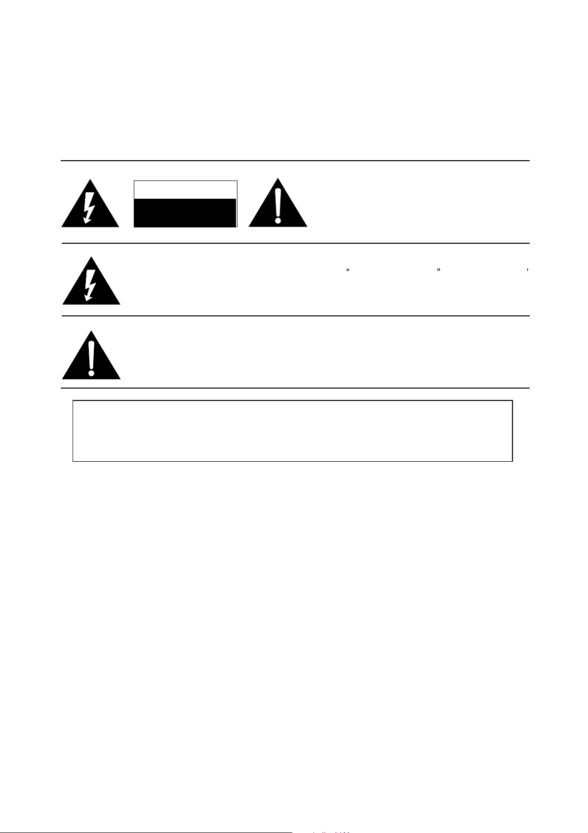
The lighting flash with arrowhead symbol, with an equilateral triangle is intended to
alert the user to the presence of uninsulated voltage within the products
enclosure that may be of sufficient magnitude to constitute a risk of electric shock to
the person.
The exclamation point within an equilateral triangle is intended to alert the user to the
presence of important operating and maintenance (servicing) instructions in the
literature accompanying the appliance.
ELECTR ICAL SHOCK, DO NOT RE MOVE
COVER (OR BACK). NO USER SERVICEABLE
PAR TS INS IDE . RE FE R SE R VIC ING TO
QUALIFIE D SERVIC E PERSONNEL.
dangerous
WARNING: TO REDUCE RISK OF FIRE OR ELECTRIC SHOCK, DO NOT
EXPOSE THIS APPLIANCE TO RAIN OR MOISTURE.
2
Page 3

SCHNEIDER ELECTRONICS GMBH-GERMANY
3
IMPORTANT SAFETY INSTRUCTIONS
CAUTION:
Read all of these instructions. Sa ve these instructions for later use . Follo w all W arnings and
Instructions marked on the audio equipment.
1. Read Instructions-All the safety and operating instructionsshouldbe read before the productis operated.
2. Retain Instructions- The safety and operating instructions should be retained for future reference.
3. Heed Warnings- All warnings on the product and in the operating instructions should be adhered to.
4. Follow Instructions- All operating and use instructions should be followed.
FOR YOUR PERSONAL SAFETY
1. When the power cord or plug is damaged or frayed, unplug this television set from the wall outlet and refer servicing to
qualified service personnel.
2. Do not overload wall outlets and extension cords as this can result in fire or electric shock.
3. Do not allow anything to rest on or roll over the power cord, and do not place the TV where power cord is subject to
traffic or abuse. This may result in a shock or fire hazard.
4. Do not attempt to service this television set yourself as opening or removing covers may expose you to dangerous
voltage or other hazards. Refer all servicing to qualified service personnel.
5. Never push objects of any kind into this television set through cabinet slots as they may touch dangerous voltage
points or short out parts that could result in a fire or electric shock. Never spill liquid of any kind on the television set.
6. If the television set has been dropped or the cabinet has been damaged, unplug this television set from the wall outlet
and refer servicing to qualified service personnel.
7. If liquid has been spilled into the television set, unplug this television set from the wall outlet and refer servicing to
qualified service personnel.
8. Do not subject your television set to impact of any kind. Be particularly careful not to damage the picture tube surface.
9. Unplug this television set from the wall outlet before cleaning. Do not use liquid cleaners or aerosol cleaners. Use a
damp cloth for cleaning.
10.1. Do not place this television set on an unstable cart, stand, or table. The television set may fall, causing serious injury
to a child or an adult, and serious damage to the appliance. Use only with a cart or stand recommended by the
manufacturer, or sold with the television set. Wall or shelf mounting should follow the manufacturer s instructions, and
should use a mounting kit approved by the manufacturer.
10.2. An appliance and cart combination should be moved with care. Quick stops, excessive force, and uneven surfaces
may cause the appliance and cart combination to overturn.
3
Page 4
SCHNEIDER ELECTRONICS GMBH-GERMANY
4
PROTECTION AND LOCATION OF YOUR SET
11. Do not use this television set near water ... for example, near a bathtub, washbowl, kitchen sink, or laundry tub, in a
wet basement, or near a swimming pool, etc.
Never expose the set to rain or water. If the set has been exposed to rain or water, unplug the set from the wall
outlet and refer servicing to qualified service personnel.
12. Choose a place where light (artificial or sunlight) does not shine directly on the screen.
13. Avoid dusty places, since piling up of dust inside TV chassis may cause failure of the set when high humidity persists.
14. The set has slots, or openings in the cabinet for ventilation purposes, to provide reliable operation of the receiver, to
protect it from overheating. These openings must not be blocked or covered.
Never cover the slots or openings with cloth or other material.
Never block the bottom ventilation slots of the set by placing it on a bed, sofa, rug, etc.
Never place the set near or over a radiator or heat register.
Never place the set in enclosure, unless proper ventilation is provided.
a built-in
PROTECTION AND LOCATION OF YOUR SET
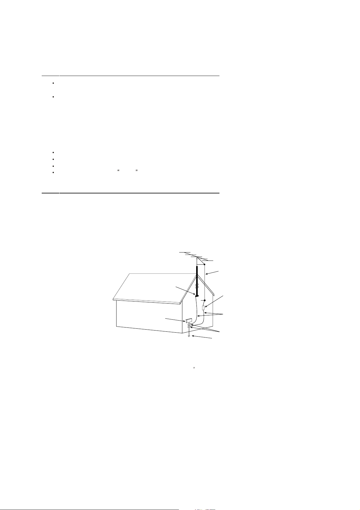
15.1. If an outside antenna is connected to the television set, be sure the antenna system is grounded so as to provide some
protection against voltage surges and built up static charges, Section 810 of the National Electrical Code, NFPA No.
70-1975, provides information with respect to proper grounding of the mast and supportingstructure, grounding of the
lead-in wire to an antenna discharge unit, size of grounding conductors, location of antenna discharge unit, connection
to grounding electrode, and requirements for the grounding electrode.
EXAMPLE OF ANTENNA GROUNDING AS PER NATIONAL ELECTRICAL CODE INSTR UCTIONS
EXAMPLE OF ANTENNA GROUNDING AS PER
NATIONAL ELECTRICALCODE
ANTENNA
LEAD- IN WIRE
GROUND CLAMP
ELECTRIC SERVICE
EQUIPMENT
NEC-NATIONAL ELECTRICALCODE
ANTENNA DISCHARGE
UNIT (NEC SECTION
810-20)
GROUNDING
CONDUCTORS
(NECSECTION 810-21)
GROUND CLAMPS
POWER SER VICE GROUNDING
ELECTRODE SYSTEM
(NEC ART 250. PART H)
15.2. Note to CATV system installer : (Only for the television set with CATV reception)
This reminder is provided to call the CATV system attention to Article 820-40 of the NEC that provides
installer s
guidelines for proper grounding and, in particular, specifies that the cable ground shall be connected to the grounding
system of the building, as close to the point of cable entry as practical.
16. An outside antenna system shouldnot be located in the vicinity of overhead power lines or other electric lights or power
circuits, or where it can fall into such power lines or circuits. When installing an outside antenna system, extreme care
should be taken to keep from touching such power lines or circuits as contact with them might be fatal.
17. For added protection for this television set during a lightning storm, or when it is left unattended and unused for long
periods of time, unplug it from the wall outlet and disconnect the antenna. This will prevent damage due to lightning
and power-line surges.
4
Page 5

SCHNEIDER ELECTRONICS GMBH-GERMANY
5
OPERATION OF YOUR SET
18.
This television set should be operated only from the type of power source indicated on the marking label.If you are not
sure of the type of power supply at your home, consult your television dealer or local power company. For television
sets designed to operate from battery power, refer to the operating instructions.
19. If the television set does not operate normally by following the operating instructions, unplugthis television set from the
wall outlet and refer servicing to qualifiedservice personnel. Adjust only those controls that are covered in the operating
instructions as improper adjustment of other controls may result in damage and will often require extensive work by a
qualified technician to restore the television set to normal operation.
20. When going on a holiday : If your television set is to remain unused for a period of time, for instance, when you go on
a holiday, turn the television set and unplug the television set from the wall outlet.
off
IF THE SET DOES NOT OPERATE PROPERLY
21. If youare unable to restore normaloperation by followingthe detailedprocedurein your operating instructions,
do not attempt any further adjustment. Unplug the set and call your dealer or service technician.
22. Whenever the television set is damaged or fails, or a distinct change in performance indicates a need for
service, unplug the set and have it checked by a professional service technician.
23. It is normal for some TV sets to make occasional snapping or popping sounds, particularly when being
turned on or off. If the snapping or popping is continuous or frequent, unplug the set and consult your
dealer or service technician.
FOR SERVICE AND MODIFICATION
24. Do not use attachments not recommendedby the television set manufacturer as they may cause hazards.
25. When replacementparts are required, be sure the service technician has used replacement parts specified
by the manufacturer that have the same characteristics as the original part. Unauthorized substitutions
may result in fire, electric shock, or other hazards.
26. Upon completion of any ser vice or repairs to the television set, ask the service technician to perform
routine safety checks to determine that the television is in safe operating condition.
5
Page 6
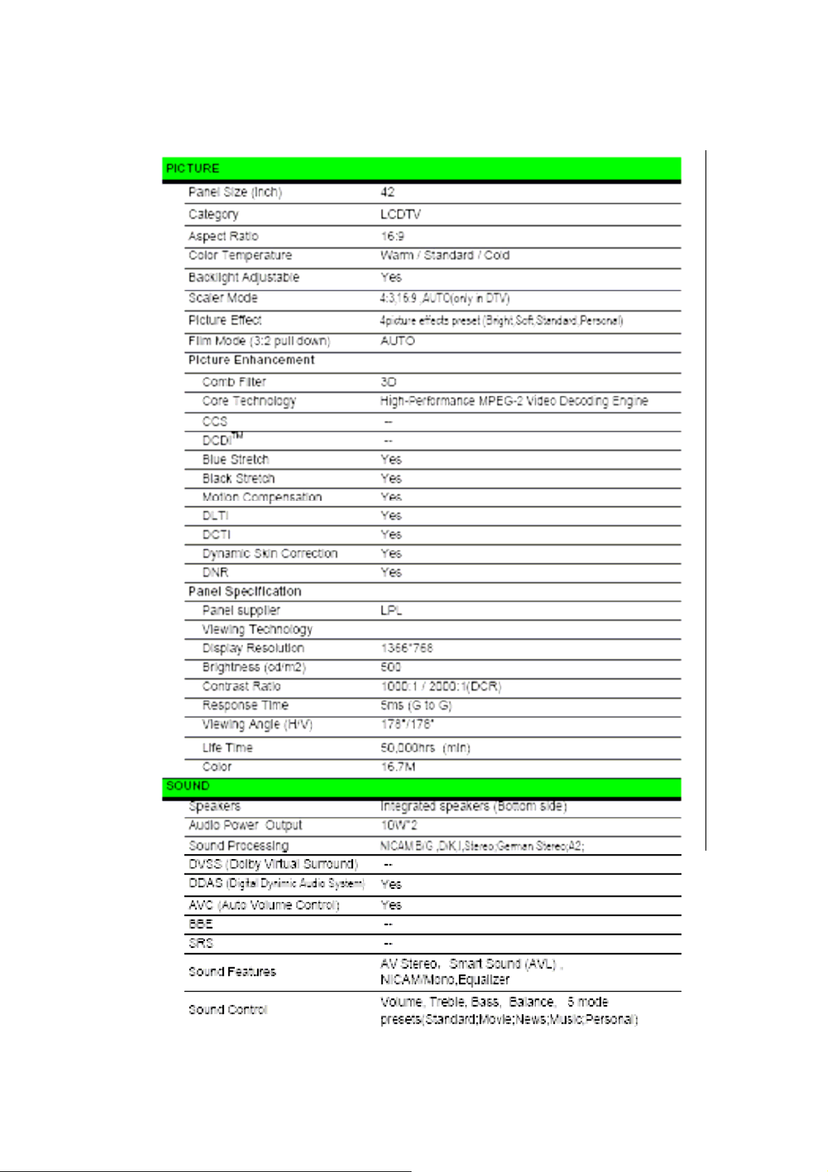
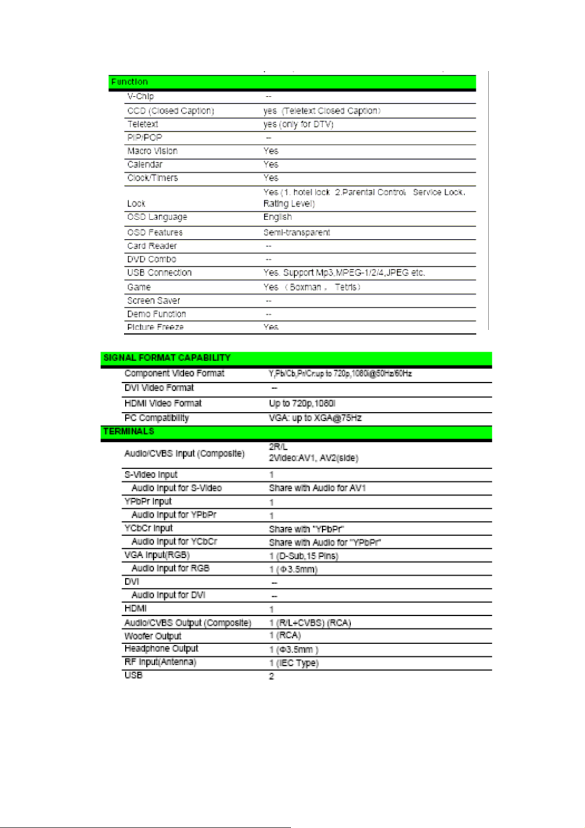
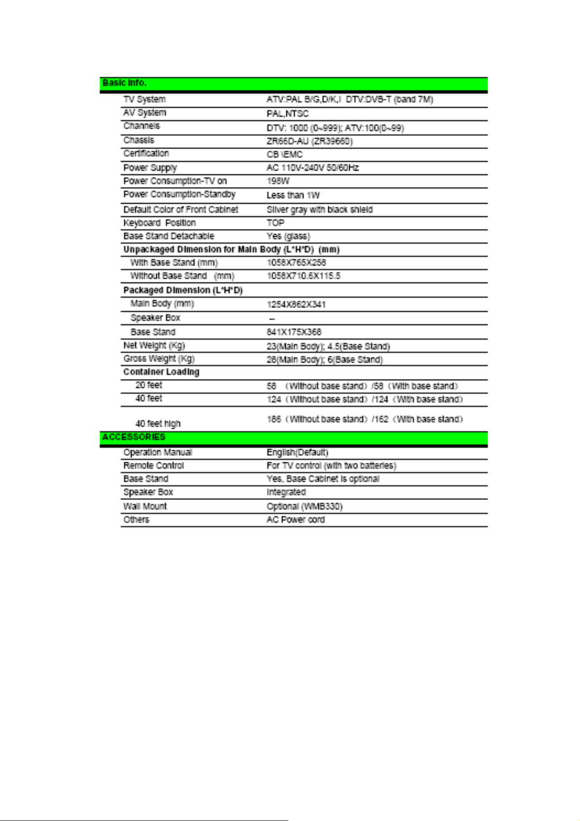
2:Product Specification
6
Page 7
7 8
Page 8
Page 9
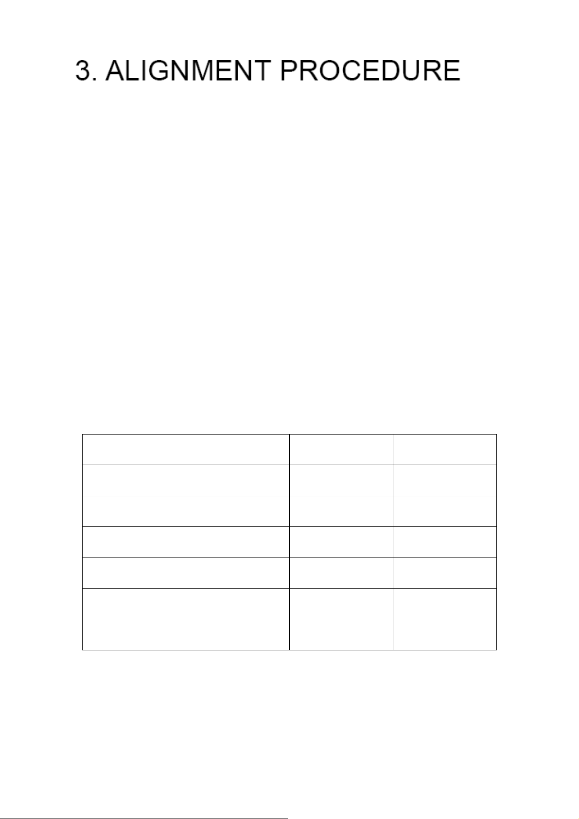
Alignment Procedure
To enter the factory mode
1.press the vol.- botton to 0 , enter the “picture” menu,cursor place the “ contrast”, input the figure
9735.
2. When using the heat key to open the factory menu , press the Freeze key if it is not
the menu .
Factory menu white balance adjust and HDMI signal source inspection
It is only adjusting whie balance of the HDMI signal source
Adjustment in HDMI mode
1. Input HDMI signal: timing is 720P, Patter is 10 grey
2. enter the factory menu, select white balance item, press OK key , system auto convering to
HDMI signal source, and so on setting the color temperure item is standard
3. adjusting the white balance machine ,setting the color coordinate to adjust the color
temperarture
4. press OK key to auto adjusting, until cuing is finishing
5. Looking into the figue and screen menu , estimating screen menu or not in gear, exit the
factory menu and inspecting the HDMI signal source
Accessory1: all the displaying item signification
X/y: about standard color temperature of the color coordinate, it is manual setting
before adjusting the white balance .
OSD display Adjust attribute and
signification
Rgain Red base gain ,according to
Adjusting of repairing
GGain Green base gain ,according to
Adjusting of repairing
BGain Blue base gain ,according to
Adjusting of repairing
Roffset Red base offset ,according to
Adjusting of repairing
Roffset Blue base offset ,according to
Adjusting of repairing
Roffset green base offset ,according to
Adjusting of repairing
Accessory2: manual adjustment mode
The coursor placed to x or y,press “OK” key to enter manual adjustment of the white
banlace
(2).the ADC in the factory menu is been adjusted and inspecting YpbPr /VGA/AV
signal source
only auto adjusting the YpbPr/VGA/AV signal source ,all signal source adjustment mode as
.
Adjust range Windows default
0~~100 50
0~~100 50
0~~100 50
0~~100 50
0~~100 50
0~~100 50
9
Page 10
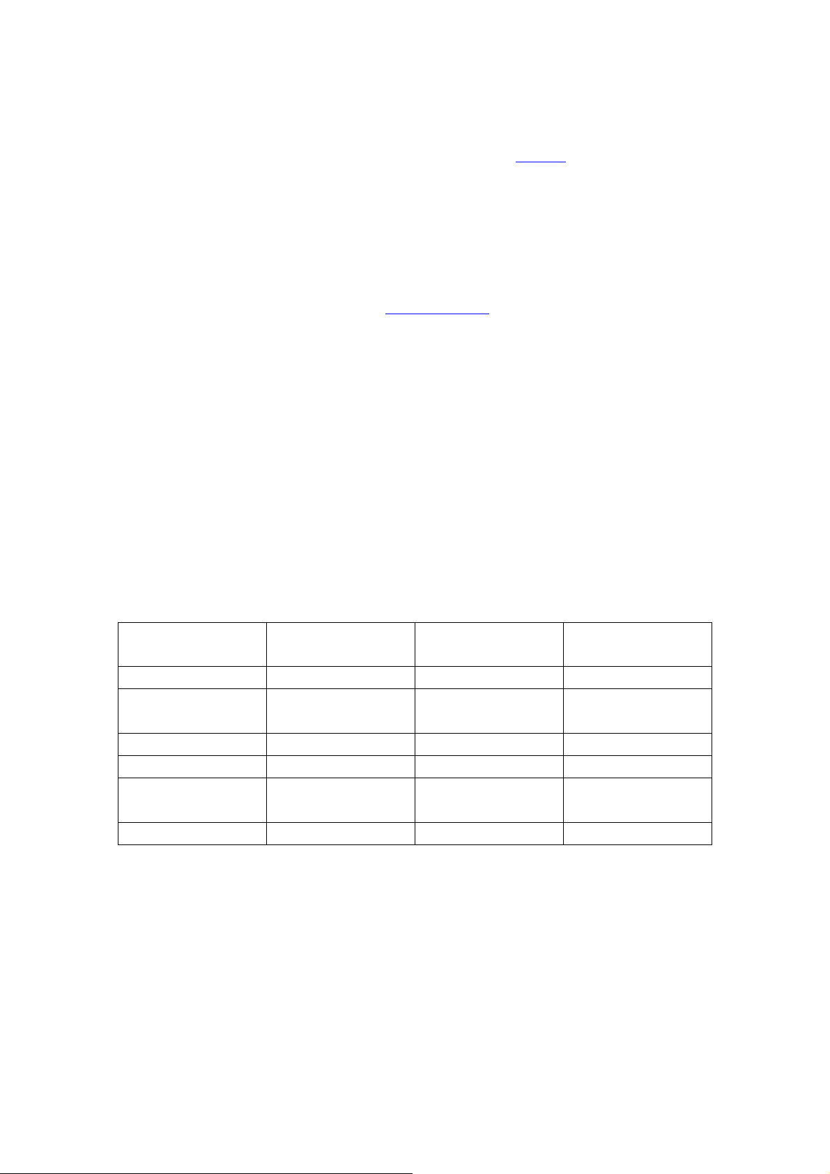
follows:
10
1. Y pbPr
a. switching to YpbPr signal source ,input the
eight grey-scale/color –bar signal
reference machine model: timing81 of bsg360a, pattern85
b. enter the ADC of the factory menu item ,press OK key to auto adjusting
c. after cuing auto ajustment successfully,observing displaying figue and screen
menu or not in gear, exit the factory menu ang inpect the YpbPr signal source .
2.VGA
a. Switching to VGA signal source , input
reference machine model: BSG360A of Timing13,pattern105
b. enter the factory menu ADC item ,press ok key to auto adjusting
c. after cuing auto ajustment successfully, ovserving successfully, observing displaying figue
and screen menu or not in gear, exit the factory menu ang inpect the VGA signal source
3.AV
d. Switching to AV signal source , input PAL 、100% saturation of the 8 grey signal source
reference machine model: BSG360A of Timing72,pattern 85
e. enter the factory menu ADC item ,press ok key to auto adjusting
f. after cuing auto ajustment successfully, ovserving successfully, observing displaying figue
and screen menu or not in gear, exit the factory menu ang inpect the AV signal source
4、Inspect ATV/DTV signal source
parting switch to ATV or DTV ,and then scaning,ovserving or not losing channel and the
picture displaying and volume in gear or not
5、the factory menu function setting
OSD display Adjusting attribute
and signification
LCD panel type LCD screen select LPL/AUO/CMO LPL
Factory Menu Hotkey Factory menu heat
key
Hotel mode Hotel mode switch On/off Off
Power on mode Electrify mode Stv/on/last Stb
Default value reset Reset factory setting
data
Factory init Leave factory setting -----------
1) according to so you saying item: enactment LCD panel factory appellation,
factory menu heat key setting to OFF, hotel mode setting to off; Electrify
mode setting to STB
2) select factory init item, press ok key to initialization operating about
boot-strap
WARNING: during finishing the Factory init operating to packing , if
the TV han been boot-straped , the TV must operate again before
packing
1024x768@60Hz 16 grey or 10 grey
Range or range Windows default
On/off Off
------
720@60 contrast of 100%
Page 11

4.BOM LIST
MODEL:LCD32M61AZ
4.1
PART NO. SEPC QTY LOCATION
08-LON37A-PW1W ASS'Y - POWER BD 1
09-55C15V-DTX SMD.DIODE BZV55-C15 3 D1003;D806;D825
09-55C18V-DTX SMD.DIODE BZV55-C18 3 D807;D823;D880
09-55C5V1-DTX SMD.DIODE BZV55-C5V1 1 D1000
09-LL4148-ATX SMD. SWITCHING DIODE LL4148 8
D1004;D1005;D808;D809;D814;D819;
D820;D826
09-RLZ9B1-DTX SMD. ZENER DIODE RLZ9.1B 1 D1002
10-0SR360-F0X DIODE SR360 3A/60V 1 D817
10-1N4007-EBX DIODE IN4007 3 D810;D822;D824
10-20100C-F7X DIODE MBR20100CT(TO-220) 1 D805
10-20CT15-S7X DIODE 20CTQ150 TO-220AB 2 D802;D803
10-HER108-FBX DIODE HER108 1 D818
10-A1106S-F7X DIODE FMXA-1106S 1 D801
10-MUR460-F0X DIODE MUR460 (FAST RECOVERY) 2 D811;D812
10-RS1505-H7X DIODE RS1505M 1 BD801
11-20NM50-0AX TRANSISTOR STW20NM50 1 Q801
11-SK3568-0CX TRANSISTOR 2SK3568 2 Q803;Q806
12-BT3904-0BX SMD. TRANSISTOR MMBT3904LT1(NPN) 5 Q1001;Q802;Q808;Q812;Q1
12-S5160T-0BX SMD.TRANSISTOR PBSS5160T 2 Q1000;Q807
12-BT3906-0BX SMD. TRANSISTOR MMBT3906LT1(PNP) 3 Q1002;Q805;Q810
13-000TL4-31T IC TL431ACLP 3 Q804;Q809;Q811
13-0HPC92-2BP TCL13-0HPC92-2BP= IC HPC922B R=N 3 U1;U2;U3
13-LM393D-STB IC SM LM393D(ST00) R 1 U7
13-NCP137-7BB PWM IC NCP1377B 1 U5
13-NCP165-3AB PFC IC NCP1653ADR2G 1 U6
13-VIPER2-2AP IC VIPER22ADIP-E 1 U4
18-FF0563-JGX RES. M.O. 56K OHM 1W +/-5% 1 R835
18-FG0470-JHX RES. M.O. 47 OHM 2W +/-5% 1 R832
18-GJ0351-JVX RES.CEMENT 350 OHM 5W +/-5% 3 R6;R4;R5
18-KE0684-JNX RES.GLASS GLAZE 680K 1/2W +/-5% 1 R825
18-KF0825-JHX RES. GLASS GLAZE 8.2M OHM 1W 2 R2;R853
18-MJ0228-JDX RES.C.C. 5W 0.22OHM +/-5% 1 R834
18-NH0108-JLX RES.C.C NKN3W +/-5% 0R1 M15 1 R801
18-P40805-00X RES. 5MΩ 1 R910
19-BB0000-JTX SMD. RES 0 OHM 1/10W +/-5% 14
R890;R1040;R600;R7;R8;R851;R13;R
17;R18;R907;R909;R20;R23;R24
19-CD0330-JTX SMD. RES 33 OHM 1/4W +/-5% 3 R868;R829;R815
19-BB0100-JTX RES. SMD 10 OHM 1/10W +/-5% 2 R847;R813
19-BB0101-JTX SMD. RES 100 OHM 1/10W +/-5% 1 R902
19-BB0102-JTX SMD. RES 1K OHM 1/10W +/-5% 8
19-BB0103-JTX SMD. RES 10K OHM 1/10W +/-5% 12
R903;R905;R906;R1002;R1003;R1005
;R838;R842
R802;R1009;R809;R804;R805;R816;R
833;R836;R841;R843;R844;R900
19-BB0683-JTX SMD. RES 68K OHM 1/10W +/-5% 2 R1000;R828
19-BB0104-JTX SMD. RES 100K OHM 1/10W +/-5% 1 R1007
19-BB0105-JTX SMD. RES 1M OHM 1/10W +/-5% 0805 5 R860;R864;R865;R3;R1
11
Page 12

4.BOM LIST
12
MODEL:LCD32M61AZ
19-BB0122-JTX SMD. RES 1.2K OHM 1/10W +/-5% 1 R837
19-BB0123-JTX SMD. RES 12K OHM 1/10W +/-5% 1 R856
19-BB0201-JTX SMD. RES 200 OHM 1/10W +/-5% 1 R830
19-BB0202-JTX SMD. RES 2K OHM 1/10W +/-5% 0805 1 R1004
19-BB0153-FTX RES.SMD 15KOHM 1/10W +/-1% 1 R808
19-CD0220-JTX SMD. RES 22 OHM 1/4W +/-5% 1206 1 R826
19-CD0000-JTX RES.SMD 0 OHM 1206 7 R831;R9;R14;R15;R16;R827;R850
19-BB0220-JTX SMD. RES 22 OHM 1/10W +/-5% 1 R880
19-BB0223-JTX SMD. RES 22K OHM 1/10W +/-5% 1 R820
19-BB0242-JTX RES. SMD 2.4K OHM 1/10W +/-5% 1 R839
19-BB0392-FTX SMD.RES. 1/10W 3.9KOHM +/-1% 2 R822;R821
19-BB0272-JTX SMD. RES 2.7K OHM 1/10W +/-5% 2 R869;R22
19-BB0332-JTX SMD. RES 3.3K OHM 1/10W +/-5% 1 R1006
19-BB0333-JTX SMD. RES 33K OHM 1/10W +/-5% 2 R845;R1008
19-BB0364-JTX SMD.RES 360K OHM 1/10W +/-5% 1 R867
19-BB0471-JTX SMD. RES 470 OHM 1/10W +/-5% 1 R803
19-BB0472-JTX SMD. RES 4.7K OHM 1/10W +/-5% 2 R857;R848
19-BB0473-FTX SMD. RES 47K OHM 1/10W 1% 0805 1 R904
19-BB0333-FTX SMD. RES 33K OHM 1/10W +/-1% 1 R811
19-BB0473-JTX SMD. RES 47K OHM 1/10W +/-5% 1 R812
19-BB0512-FTX SMD. RES 5.1K OHM 1/10W +/-1% 2 R840;R855
19-BB0563-JTX SMD. RES 56K OHM 1/10W +/-5% 1 R870
19-BB0621-JTX SMD. RES 620 OHM 1/10W +/-5% 1 R908
19-BB0684-JTX SMD. RES 680K OHM 1/10W +/-5% 1 R901
19-BB0689-JTX SMD. RES 6.8 OHM 1/10W +/-5% 1 R859
19-BB0753-JTX RES. SMD 75K OHM 1/10W J 0805 1 R858
19-BB0912-JTX SMD. RES 9.1K OHM 1/10W +/-5% 1 R1001
19-CD0224-FTX 1206 SMD.RES.220K OHM 1% 1/4W 1 R866
19-CD0684-FTX SMD.RES 680K OHM 1/4W +/-1% 1 R861
19-CD0474-FTX SMD. RES 470K OHM 1/4W +/-1% 2 R862;R863
22-NTC259-XH0 NTC 2.5D-18LCS 1 R824
22-VDR561-XG2 VARISTOR RESISTANCE 14D561K-M 1 RV801
25-GCA102-M1P CAP.ELEC 1000UF 16V +/-20% 1 C827
25-GCB470-M1X CAP. ELEC 47 UF 16V +/-20% 105 1 C1001
25-GDA222-M1X CAP ELEC 2200UF 25V +/-20% 105 2 C804;C809
25-GEA471-M1P CAP.ELEC. 470UF 35V +/-20% 1 C805
25-GFB100-M1X CAP. ELEC 10 UF 50V +/-20% 1 C822
25-GFB229-M1X CAP ELEC 2.2UF 50V +/-20% 105 2 C842;C1010
25-GFB330-M1X CAP.ELEC 33UF/50V RGA330M1HTA- 1 C836
25-GFB479-M1XH
25-GMA220-M1S CAP ELEC RGA/400V/22UF 12.5X25 1 C825
25-GNJ331-M1S CAP. ELEC 330UF/450V+/-20% 1 C807
25-MDB100-K1X CAP.ELEC 10UF 25V +/-10% 1 C843
25-NDA471-M1X CAP. ELEC 25V/470UF+/-20% 1 C810
25-NEF222-M1X CAP.ELEC 2200UF 35V +/-20% 2 C802;C803
26-AKC221-KRX CAP.CER 220PF 1KV +/-10% 1 C852
CAP.ELEC4.7UF/50V/+/20%RXW4R7M1HBK-0611
1 C1011
Page 13

4.BOM LIST
13
MODEL:LCD32M61AZ
26-AKL103-MEX CAP.CER 10NF 1KV 1 C824
26-AKM221-KRX CAP. CER 220 PF 1KV +/-10% 1 C806
26-AKM471-KRX CAP. CER 470 PF 1KV +/-5% SL 2 C850;C851
26-APK102-MEX CAP. CER 1000PF 400VAC +/-20%E 4 C1;C814;C815;C832
27-AQT105-MVG CAP. M.PP 1UF/275VDC/+/-20% 1 C819
27-AWQ474-J0X CAP.PP MPP-474J2WC15C4 1 C801
28-BB0102-KBX SMD CAP. 0.001UF 50V B 0805 5 C846;C849;C839;C817;C838
28-BB0104-ZFX
28-BB0105-ZFX SMD. CAP 1UF 50V +80%-20% 4 C844;C904;C837;C820
28-BB0103-ZFX SMD CAP. 0.01 UF 50V F 0805 1 C818
28-BB0220-JCX SMD.CAP 22 PF 50V C 0805 1 C840
28-BB0222-KBX SMD CAP 0.0022UF 50V +/-10% 1 C847
28-BB0479-CCX SMD. CAP 4.7pF 50V +/-0.25PF 1 C1002
28-BD0225-ZFX SMD.CAP 2.2UF/25V 2 C901;C1000
35-FB1690-30X MAGNETIC CORE 4
41-WJ0100-B00 WIREBAREJUMPER10MM 4 LB801;LB802;J9;J1
36-LIF126-AX0 PFC COIL TE3521A6200 1 L801
36-LIF129-XX0 LINE FILTER LCL-2425 2 LF801;LF802
36-TRF263-AX1 TRANSFORMER CONV. BCK-4609A 1 T801
36-TRF280-AX0 TRANSFORMER CONV.(2215) BCK-2215 1 T803
36-WID249-XX0 COIL WIDTH 2.4UH FLC0514 1 L802
36-WID629-XX1 COIL CHOKE 6.2UH 1 L804
40-MON37A-PWD1X P.C.B POWER BD 1
41-WJ0080-B00 WIREBAREJUMPER8MM 4 J7;J3;J10;J12
41-WJ0110-B00 WIREBAREJUMPER11MM 1 J22
41-WJ0120-B00 WIREBAREJUMPER12MM 4 J27;J29;J6;J2
41-WJ0140-B00 WIREBAREJUMPER14MM 2 J16;J20
41-WJ0150-B00 WIREBAREJUMPER15MM 4 J33;J18;J35;J11
41-WJ0160-B00 WIREBAREJUMPER16MM 1 J23
41-WJ0180-B00 WIRE BARE JUMPER 18MM 1 J5
41-WJ0195-B00 WIREBAREJUMPER19.5MM 5 J15;J28;J4;J8;J21
41-WJ0220-B00 WIRE BARE JUMPER 22MM 1 J25
46-35063W-03XG PIN BASE *3 VH-3A 1 P801
46-35199W-03XG PIN BASE *3 PITCH=2.0MM 1 P802
46-35200W-04XG CONN. VH-4A 4PIN PITCH=3.96MM 1 P803
46-35200W-05XG BASE 5PIN 1 P804
50-05000D-RUT1G FUSE 5RT 250V 5A 1 F801
54-315110-000 MICA SHEET (20MMX24MMX0.1MM) 1 FOR Q801
54-315250-000 TRANSMIT HOT SILICA GEL 3 FOR D802;FOR D803;FOR D805
54-315260-000 BUSHING TO-220B (3MMX 2.5MM) 3 FOR D805;FOR D803;FOR D802
54-38271X-0U0 PYROCONDENSATION BUSHING 8MM 0.01 FOR F801
58-829590-0UH PVC FIBER SINK 2
SMD CAP. 0.1 UF 50V +80/-20%
0805
C848;C900;C845;C902;C903;C841;C8
14
33;C831;C829;C828;C811;C1004;C10
03;C2
FOR Q803 D pin;FOR Q806 D;FOR
D801 ;FOR Q801 D极
FOR 67-H82962-3A0&67-H82963-
1A0;FOR 67-H82962-1A0&67-H82963-
2A0
Page 14

4.BOM LIST
14
MODEL:LCD32M61AZ
64-B30080-104G M/C SCREW B 3 X 8 7
64-B30100-104G M/C SCREW B 3 X 10 1 FOR Q801
64-F30080-103G M/C SCERW F 3 X 8 9
64-Z30080-112G MACHINE SCREW 6
66-343730-0B0 HOLLOW RIVET 1.6MMX3.0MMX3.2MM 16
66-343740-0B0 HOLLOW RIVET (2.3MMX4.0MMX3.5MM) 2 FOR C807
67-H82960-0A0 HEAT SINK 1 FOR 67-H82963-1A0&67-H82963-2A0
67-H82961-0A0 HEAT SINK 1 FOR 67-H82962-1A0&67-H82962-3A0
67-H82962-1A0 HEAT SINK 1 FOR BD801&Q801&D801
67-H82962-3A0 HEAT SINK 1 FOR Q803&Q806
67-H82963-1A0 HEAT SINK 1 FOR D802&D803
67-H82963-2A0 HEAT SINK 1 FOR D805
67-M60442-0E0 METAL PART 4 H01;H02;H03;H04
36-HDR050-XX0 TRANSFORMER HORIZ DRIVE BCT- 1 T802
71-268390-0A0AFLABEL (QC) GREEN 1
71-3507MM-NUL9ALABEL 1
27-AQQ224-MV6 CAP. M.PP 0.22 UF 250VAC +/-20% 1 C100
19-CD0472-JTX SMD. RES 4.7K OHM 1/4W 5% 1 R21
19-CD0471-JTX SMD. RES 470 1/4W 5% 1 R25
19-CD0122-JTX SMD.RES 1.2K OHM 1/4W +/-5% 1 R26
T8-HM61JZ1-BSY ASS'Y - BASE 1
59-829370-000 RUBBER PAD 6 ADHERE TO THE GLASS STAND
59-830250-000 RUBBER PAD 4
64-F60200-104G MACHINE SCREW 4 MTG GLASS STAND & STAND SUPPORT
64-H80250-104G M/C SCREW H 8 X 25 4 MTG STAND SUPPORT & BACK COVER
75-830450-CC0 POLYFOAM 2
75-830460-CC0 POLYFOAM 2
T8-HM61JZ1-BSYZ ASS'Y - BASE(ART) 1
49-827360-0001B BASE GLASS 1
68-827350-0001B BASE SUPPORT 1
74-080050-50D1B PLASTIC BAG 1 PACKING STAND GLASS
74-702360-52D9B POLYBAG (150MMX100MMX0.05MM) 1 PACKING SCREW M8
76-830470-0AT CARTON BOX 1
58-827840-00H BASE PAD 1
T8-HM61JZ1-CSY ASS'Y - CHASSIS SHIELD 1
63-B30080-AB4G S/T SCREW B 3 X 8 AB 5
FOR BD801;FOR D801;FOR D802;FOR
D803;FOR D805;FOR Q803;FOR Q806
FOR 58-829590-0UH;FOR 67-H82960-
0A0;FOR 67-H82961-0A0
FOR 67-H82963-2A0;FOR 67-H82963-
1A0;FOR 67-H82962-3A0;FOR 67-
H82962-1A0
FOR C802;FOR C803;FOR L801;FOR
T801;FOR L806
ADHERE BETWEEN SCREW AND GLASS
STAND
PLACED BETWEEN STAND SURPORT AND
STAND G
MTG REAR AV & BOTTOM
SHIELDING;MTG REAR AV & TERMINAL
PLATE
Page 15

4.BOM LIST
15
MODEL:LCD32M61AZ
FIX USB. BOARD & SHIELD;MTG
64-B30060-304G TRIANGLE M/C SCREW B 3 X 6 8
66-702620-0E2G SCREW POST 4
67-S81587-0E0 SCREEN COVER(TOP) 1
67-S81588-KE0 TERMINAL BOARD 1
67-S82483-HE0 SCREEN COVER 1
T8-0M61AZ-USY ASS'Y - USB BD 1
09-LL4148-ATX SMD. SWITCHING DIODE LL4148 1 D3
10-1N4001-EBX DIODE 1N4001 (RECTIFIER) 2 D14;D13
12-BT8050-CBX SMD. TRANSISTOR MMBT8050CLT1 1 Q4
12-ML6401-0BX MOS IRLML6401 2 Q3;Q5
13-0TG242-LPB IC 0TG242LP 1 U6
13-41632K-UCB60 SDRAM 64M K4S641632K-UC60(K-DIE) 1 U16
13-AL016M-90B
13-AML327-80B IC AML3278 1 U4
13-AS1117-ADB IC AS1117-ADX 1 U2
13-CS4334-KSB IC CS4334KS SO-8 STEREO D/A 1 U18
13-LD1117-33B IC LD1117 3.3V 1 U8
13-M24C02-MNB EEPROM M24C02WMN6TG 1 U5
13-SN74HC-14B IC SN74HC14D-SOP14 1 U12
19-AA0000-JTX RES. SMD 0 OHM 1/16W +/-5% 4 R26;R18;R9;R28
19-AA0101-JTX RES. SMD 100 OHM 1/16W +/-5% 3 R19;R54;R77
19-AA0102-JTX RES. SMD 1K OHM 1/16W +/-5% 1 R51
19-AA0103-JTX RES. SMD 10K OHM 1/16W +/-5% 9
19-AA0104-JTX RES. SMD 100K OHM 1/16W +/-5% 1 R17
19-AA0153-JTX RES.SMD 15K 1/16W 0603 +/-5% 1 R11
19-AA0201-JTX SMD. RES 200 OHM 1/16W +/-5% 1 R15
19-AA0220-JTX SMD. RES 22 OHM 1/16W +/-5% 1 R79
19-AA0222-JTX RES. SMD 2.2K OHM 1/16W +/-5% 2 R74;R73
19-AA0331-JTX RES. SMD 330 OHM 1/16W +/-5% 2 R44;R65
19-AA0472-JTX RES. SMD 4.7K OHM 1/16W +/-5% 5 R1;R3;R4;R63;R48
19-AA0514-JTX RES.SMD 510K OHM 1/16W 5% 1 R23
19-AA0750-JTX RES. SMD 75 OHM 1/16W +/-5% 4 R5;R80;R83;R93
22-PTC068-XX0 PPTC(SMD)KMCSS150RY 2 FB14;FB15
23-A08103-JBX NETWORK RES. 10K OHM +/-5% 0603 1 RN4
23-A08220-JBX NETWORK RES. 22 OHM +/-5% 1 RN1
23-A08330-JBX NETWORK RES. 33 OHM +/-5% 1 RN3
23-A08472-JBX NETWORK RES. 4.7K OHM +/-5% 1 RN2
28-AB0101-JCX SMD. CAP 100 PF 50VDC +/-5% 1 C127
28-AB0102-KBX SMD. CAP 1000 PF 50V +/-10% B 1 C3
16M FLASH IC
S29AL016M90TFI02(WRITE)
BOTTOM SHIELDING & TERMINAL
PLATE;MTG MAIN BOARD PCB &
BOTTOM SHIELDING
FIX VGA TERMINAL & SHIELD;FOR
P500
1 U15(CP)
R56;R75;R55;R50;R24;R21;R20;R16;
R14
Page 16

4.BOM LIST
16
MODEL:LCD32M61AZ
C22;C24;C25;C26;C27;C28;C29;C89;
C98;C91;C75;C74;C58;C56;C54;C51;
C48;C47;C46;C45;C43;C42;C41;C40;
C39;C21;C20;C2;C179;C177;C149;C1
48;C147;C146;C145;C144;C30;C77;C
74CAP. SMD 0.1UF 50V +80%~-20% F28-AB0104-ZFX
86;C76;C117;C116;C115;C114;C113;
C112;C110;C109;C108;C106;C105;C1
33;C134;C118;C123;C124;C125;C128
;C130;C131;C132;C101;C102;C104;C
122;C121;C120;C119;C135;C136;C13
7;C139;C142;C143
28-AB0220-JCX CAP. SMD 22PF 50V +/-5% C 2 C37;C38
28-AB0223-ZFX CAP.SMD 0.022UF 50V 80-20 0603 2 C170;C171
28-AB0470-JCX CAP.SMD 47PF 50V +/-5% 0603 6 C82;C63;C62;C182;C181;C180
28-AB0689-CCX SMD. CAP 6.8pF 50VDC +/-0.25pf 2 C50;C141
28-RC0106-MAH SMD. CAP 10 UF 16V +/-20% 3 C17;C169;C168
28-RC0107-MAH SMD. CAP 100 UF 16V +/-20% 13
28-RC0476-MAH1 SMD. CAP 47 UF 16V +/-20% 6 C4;C178;C176;C126;C111;C103
33-ELN121-NTX SMD.COLL 11
33-KLN600-NTX CHIP BEAD 60 OHM 0603 +/-25% 3 L3;L4;L5
45-OSC27M-0Y3 CRYSTAL 27MHZ 1 X1
46-38605W-10XG PIN BASE TU2005WNR-2X5 2 P5;P3(NEAR PIN13&14)
46-38605W-14XG PIN BASE TU2005WNR-2X7 1 P4
67-387190-0A0 HEAT SINK 1 FOR U4
40-L46E64-USB2X P.C.B US BD 1
45-OSC6M0-0Y1B CRYSTAL 8C20250132AHAF25Q3 1 X2
28-RC0227-MAL SMD. CAP 1 C52
T8-LDZR66-MAN ASS'Y - MAIN BD 1
02-KTX179-DAX FIBER OPTIC TRANSMITTING MODULE 1 P206
07-DVBTI5-TC3G TUNER FQD1216ME/I H-5 1 TUN1
09-0BAV70-ATX SMD DIODE BAV70 2 D400;D501
09-0BAV99-ATX HIGH SPEED DOUBLE DIODE BAV99 4 D302;D301;D509;D510
09-D5V0L4-UGB SMD.DOIDE PESD5V0L4UG 7
09-D5V0S2-BTB SMD.DOIDE PESD5V0S2BT 4 ESD205;ESD204;ESD203;ESD201
09-FM5817-STX SMD.DIODE FM5817 2 D508;D500
09-LL4148-ATX SMD. SWITCHING DIODE LL4148 5 D506;D505;D205;D206;D504
09-RLZ5B6-DTX SMD DIODE RLZ5.6BTE11 3 ZD3;ZD2;ZD1
13-TR5V0U-4DB IC PRTR5V0U4D 2 ESD301;ESD302
11-2SB772-PAX TRANSISTOR 2SB772-P(PNP) 1 Q500
12-A04803-0BX SMD.TRANSISTOR MOSFET AO4803 1 Q403
12-BT3904-0BX SMD. TRANSISTOR MMBT3904LT1(NPN) 8
12-BT3906-0BX SMD. TRANSISTOR MMBT3906LT1(PNP) 2 Q205;Q300
12-SK2158-0BX TRANSISTOR 2SK2158 4 Q502;Q501;Q301;Q302
C140;C19;C23;C44;C73;C78;C79;C10
7;C129;C138;C80;C87;C90
FB2;FB21;FB22;FB3;FB19;FB18;FB1;
FB16;FB13;FB12;FB11
ESD202;ESD403;ESD501;ESD207;ESD2
06;ESD400;ESD402
Q503;Q404;Q304;Q303;Q202;Q401;Q2
03;Q206
Page 17

4.BOM LIST
17
MODEL:LCD32M61AZ
13-GL032A-90B 32M FLASH 1 U601(CP)
13-39661B-GCB IC ZR39661BGCG 1 U1
13-638HLC-50B IC K4D551638H-LC50 2 U701;U702
13-8569GE-DSBV IC WM8569GEDS 1 U208
13-AT24C0-2BB
12-13N03L-0BX SMD.TRANSISTOR PHKD13N03LT 1 U504
13-DA8759-HVB8 IC TDA8759HV/8 1 U401
13-EF4052-BTB IC HEF4052BT(D) 1 U206
13-IA7808-AFB IC KIA7808AF 1 U204
13-IC1084-25B IC 2.5V 5A AIC1084-25CM 1 U506
13-IC16F7-16B IC P16F716 1 U500(CP)
13-IRU303-7ABS IC DC-DC IRU3037ACSPBF 1 U503
13-KIA780-5AB IC KIA7805AF 1 U205
13-L7805A-2TB IC 5V L7805ACD2T 2 U103;U102
13-LD1117-18B 1.8V REGULATOR IC LD1117S18TR 1 U104
13-LD1117-33B IC LD1117 3.3V 3 U105;U400;U505
13-M24C16-MNB IC 16K EEPROM M24C16-MN6 1 U502
13-MP1411-DHB IC MP1411DH-LF-Z 1 U507
13-MSP341-0TB IC MSP3410G(64PINS) 1 U201
13-RC4580-IDB IC RC4580IDR 1 U209
13-PA3008-D2B IC TPA3008D2 1 U202
13-PT7809-STB IC PT7M7809ST 1 U508
13-S35390-AJB IC S-35390A SOP-8 1 U501
13-PI5V33-1QB IC PI5V331QE 1 U301
13-ST232C-D0B IC ST232CD(SOP) 1 U509
13-TDA130-8TB IC TDA1308T/N2 1 U203
13-ZL1035-3QB DTV demodulator WJCE6353 1 U101
15-LED20G-XX0 CHIP LED HMF0805GDM-BR1 1 D503
15-LED20R-XX0 CHIP LED HMF0805POM-BR1 1 D100
19-AB0000-JTX RES SMD 0 OHM 1/10W +/-5% 0603 12
19-AB0100-JTX RES SMD 10 OHM 1/10W +/-5% 7
19-AB0229-JTX SMD. RES 2.2 OHM 1/10W J 0603 1 R338
19-AB0182-FTX SMD.RES 1.8K OHM 1/10W +/-1% 1 R535
19-AB0102-JTX RES SMD 1K OHM 1/10W 0603 17
19-AB0682-JTX RES SMD 6.8K OHM 1/10W 0603 14
ATMEL 2K EERROM AT24C02BN-10SU-
1.8 WRITE
1 U402(CP)
R2;R118;R238;R247;R248;R249;R250
;R423;R539;R543;R4;R5
R533;R533A;R533B;R533C;R534;R532
;R419
R261;R276;R277;R506;R222;R221;R1
23;R117;R113;R313;R560;R508;R507
29RES SMD 100 OHM 1/10W 060319-AB0101-JTX
;R257;R223;R278;R312;R562;R21A;R
20A;R505;R112;R435;R433;R427;R42
6;R258;R259;R260
R103;R269;R268;R101;R100;R504;R5
03;R501;R453;R407;R336;R531;R525
;R548;R551;R569;R239
R328;R329;R327;R326;R228;R229;R3
00;R301;R302;R303;R308;R309;R310
;R311
Page 18
4.BOM LIST
18
MODEL:LCD32M61AZ
R279;R273;R272;R237;R254;R255;R2
81;R439;R235;R220;R232;R233;R563
RES SMD 10K OHM 1/10W 060319-AB0103-JTX 33
19-AB0123-JTX SMD. RES 12K OHM 1/10 J 0603 2 R263;R405
19-AB0124-JTX SMD. RES 120K OHM 1/10 J 0603 2 R253;R403
19-AB0203-JTX RES. SMD 20K OHM 1/10W 0603 16
19-AB0180-JTX SMD. RES 18 OHM 1/10W 0603 1 R319
19-AB0202-JTX SMD. RES 2K OHM 1/10W +/-5% 0603 4 R227;R226;R549;R511
19-AB0220-JTX SMD RES 22 OHM 1/10W 0603 9
19-AB0221-JTX RES SMD 220 OHM 1/10W 0603 4 R325;R325A;R530;R335
19-AB0222-JTX RES SMD 2.2K OHM 1/10W 0603 6 R510;R509;R106;R107;R114;R115
19-AB0302-JTX SMD. RES 3K OHM 1/10W +/-5% 0603 2 R102;R540
19-AB0331-FTX SMD.RES 330 OHM 1/10W +/-1% 2 R318;R537
19-AB0331-JTX RES. SMD 330 OHM 1/10W 0603 1 R333
19-AB0332-JTX SMD RES 3.3K OHM 1/10W 0603 9
19-AB0390-JTX RES SMD 39 OHM 1/10W +/-5%0603 6 R322;R400;R321;R320;R412;R406
19-AB0391-JTX SMD RES 390 OHM 1/10W 0603 1 R334
19-AB0471-JTX SMD. RES 470 OHM 1/10W +/-5% 4 R544;R545;R570;R546
19-AB0472-FTX SMD.RES 4.7K OHM 1/10W +/-1% 2 R542;R541
19-AB0472-JTX RES SMD 4.7K OHM 1/10W 0603 17
19-AB0510-JTX RES SMD 51 OHM 1/10W 0603 2 R315;R316
19-AB0821-JTX SMD. RES 820 OHM 1/10W +/-5% 1 R418
19-AB0822-JTX SMD. RES 8.2K OHM 1/10W +/-5% 6 R230;R231;R304;R305;R306;R307
19-BB0479-JTX SMD. RES 4.7 OHM 1/10W +/-5% 3 R105;R274;R314
19-BB0750-JTX SMD. RES 75 OHM 1/10W +/-5% 16
23-A08220-JBX NETWORK RES. 22 OHM +/-5% 22
25-BDB470-M1X CAP. ELEC 47 UF 25V +/-20% 3 C266;C275;C287
25-BDB471-M1X CAP. ELEC 470 UF 25V +/-20% 1 C599
25-KCA471-M1X CAP. ELEC 470 UF 16V +/-20% 7 C522;C260;C259;CA5;CA4;CA3;CA2
27-MBC334-J0X CAP. M.P.E 0.33UF 63V +/-5% 2 C273;C281
28-AA0105-KBX SMD.CAP 1UF 10V +/-20% 15
;R219;R218;R217;R216;R215;R211;R
210;R209;R208;R104;R234;R500;R54
7;R561;R265;R256;R262;R264;R580;
R581
R266;R267;R538;R442;R205;R206;R2
00;R201;R202;R203;R207;R270;R271
;R280;R204;R402
R414;R521;R415;R108;R109;R413;R4
10;R111;R110
R528;R529;R523;R522;R437;R436;R4
60;R290;R291
R600;R701;R700;R603;R602;R601;R5
20;R524;R526;R527;R550;R416;R116
;R330;R331;R332;R404
R324;R124;R448;R449;R431;R432;R4
44;R445;R446;R447;R430;R212;R213
;R214;R275;R323
RP715;RP713;RP712;RP714;RP701;RP
700;RN405;RN404;RN403;RN402;RP71
1;RP710;RP709;RP708;RP707;RP706;
RP702;RP703;RN400;RN401;RP704;RP
C552;C551;C550;C313;C263;C553;C2
64;C265;C312;C554;C261;C262;C555
;C338;C476
Page 19
4.BOM LIST
19
MODEL:LCD32M61AZ
C218;C241;C240;C229;C202;C203;C2
11;C212;C213;C301;C302;C303;C304
27SMD CAP 2.2UF/10V/+80/-20%28-AA0225-ZFX
;C217;C299;C254;C248;C455;C309;C
457;C10;C20;C200;C201;C214;C215;
C216
28-AB0100-JCX SMD. CAP 10 PF 50VDC +/-5% 2 C516;C515
28-AB0101-JCX SMD. CAP 100 PF 50VDC +/-5% 1 C544
28-AB0102-KBX SMD. CAP 1000 PF 50V +/-10% B 9
28-AB0103-KBX SMD. CAP 0.01 UF 50V +/-10% 0603 25
28-AB0224-ZFX CAP.SMD 0.22UF 50V +80-20%0603 4 C278;C274;C269;C268
28-AB0154-ZFX CAP.SMD 0.15UF 50V +80-20 0603 2 C535;C150
28-AB0151-JCX SMD. CAP 150 PF 50V +/-5% C 2 C13;C15
28-AB0180-JCX SMD. CAP 18 PF 50V +/-5% 0603 1 C513
28-AB0220-JCX CAP. SMD 22PF 50V +/-5% C 7
28-AB0221-JCX CAP.SMD 220PF 50V C 0603 +/-5% 1 C283
28-AB0222-KBX CAP.SMD 2200PF 50V +/-10% 0603 1 C527
28-AB0270-JCX SMD. CAP 27 PF 50V +/-5% 0603 4 C113;C114;C506;C508
C242;C239;C238;C12;C14;C107;C100
;C110;C243
C534;C526;C443;C442;C436;C435;C4
34;C433;C432;C431;C430;C439;C440
;C441;C545;C661;C558;C429;C247;C
236;C222;C126;C120;C437;C438
C505;C507;C504;C503;C501;C509;C5
10;C512;C514;C523;C525;C148;C659
;C655;C654;C651;C646;C128;C125;C
122;C119;C116;C529;C626;C623;C62
2;C621;C619;C618;C615;C614;C613;
C531;C500;C466;C464;C461;C458;C4
56;C454;C452;C451;C450;C449;C448
;C708;C705;C704;C703;C702;C701;C
700;C663;C660;C725;C724;C723;C72
2;C721;C720;C719;C718;C715;C714;
C713;C712;C635;C709;C109;C106;C1
02;C101;C16;C728;C727;C147;C146;
159CAP. SMD 0.1UF 50V +80%~-20% F28-AB0104-ZFX
C145;C144;C141;C139;C138;C137;C1
36;C135;C134;C131;C726;C711;C710
;C419;C403;C290;C284;C258;C252;C
234;C221;C220;C209;C207;C204;C15
4;C153;C332;C326;C325;C324;C323;
C322;C321;C311;C420;C412;C411;C4
10;C413;C414;C415;C409;C408;C407
;C406;C405;C404;C447;C445;C428;C
427;C426;C425;C424;C423;C422;C42
1;C547;C556;C557;C606;C636;C638;
C639;C643;C644;C607;C608;C609;C2
97;C295;C293;C291;C627;C631;C633
;C533;C538;C539;C542;C560
C104;C111;C112;C103;C330;C459;C4
60
Page 20
4.BOM LIST
20
MODEL:LCD32M61AZ
28-AB0271-JCX SMD. CAP 270 PF 50V +/-5% C 1 C328
28-AB0331-JCX SMD. CAP 330 PF 50V +/-5% 0603 1 C329
28-AB0339-CCX SMD.CAP. 50V 3.3PF +/-0.25PF 2 C228;C227
28-AB0470-JCX CAP.SMD 47PF 50V +/-5% 0603 4 C315;C511;C317;C316
28-AB0471-JCX CAP.SMD 470PF 50V +/-5% 0603 4 C256;C521;C255;C246
28-AB0560-JCX SMD CAP. 56 PF 50V +/-5% 0603 3 C224;C225;C226
28-BA0335-ZFX SMD.CAP 3.3UF 10V +80% -20% 1 C251
28-BB0104-KBX SMD. CAP 0.1UF 50VDC +/-10% 0805 8
28-BD0105-KBX SMD.CAP. 25V 1UF +/-10% 4 C288;C519;C282;C546
28-BD0225-ZFX SMD.CAP 2.2UF/25V 4 C277;C276;C270;C267
28-RC0107-MAX SMD. CAP 100 UF 16V +/-20% 4 C206;C210;C115;C121
28-RF0107-MAL1 SMD.CAP 100UF 6.3V 9
28-RF0227-MAL SMD.CAP 220UF 6.3V 9
28-RF0476-MAX SMD. CAP 47 UF 6.3V +/-20% 7
33-ELL189-KTX SMD. COIL 1.8 UH +/-10% 0805 1 L301
33-ELN121-NTX SMD.COLL 25
33-XLL150-MTX SHIELD SMD. INDUCTOR 15 UH +/- 3 L500;L503;L403
33-TLL330-MTX SMD COLL 33UH SPI124QR-330 4 L204;L205;L206;L207
36-WID100-XX5 COIL WIDTH RL0813-100M/G931 1 L502
45-OSC18M-4N0C CRYSTAL 7D1B432203BHAF50Q5 1 Y1
45-OSC20M-4Y2C CRYSTAL 7D20480243BHAF25Q3 1 X101
45-OSC24M-5N4 CRYSTAL 24.576MHZ 1 X502
45-OSC32K-7Y0 CRYSTAL 32.768KHZ 1 X501
45-OSC8M0-0Y2CB CRYSTAL TD08000333BIAF70Q5 1 X500
46-33079W-04XG PIN BASE *4 TJC3-4A 1 CN202
46-33333W-04XG PIN BASE VH-AW 1 CN503
46-35199W-03XG PIN BASE *3 PITCH=2.0MM 1 CN502
46-35199W-05XG CONN.PH-5A 5PIN PITCH=2.0MM 1 CN500
46-35199W-04XG CONN.PH-4A 4PIN PITCH=2.0MM 1 CN401
46-35199W-07XG CONN.PH-7A PITCH=2.0MM 7PIN 1 CN501
46-35199W-10XG CONN. PH-10 10PIN PITCH=2.0MM 1 CN201
46-38605W-10XG PIN BASE TU2005WNR-2X5 1 CN402
C280;C279;C271;C272;C520;C518;C5
17;C286
C307;C306;C305;C298;C463;C130;C1
32;C133;C143;C219;C296;C294;C637
;C223;C235;C249;C250;C308;C642;C
645;C650;C657;C706;C124;C707;C71
5228-CF0106-ZFX CAP. 10 UF 6.3V +80-20% 1206
6;C524A;C417;C418;C292;C289;C717
;C524;C401;C327;C462;C108;C105;C
446;C453;C118;C18;C19;C17;C11;C5
37;C543;C548;C601;C610;C611;C629
C21;C127;C502;C528;C530;C257;C20
8;C142;C140
C402;C400;C331;C129;C123;C117;C5
32;C541;C540
C244;C310;C245;C444;C320;C319;C3
18
L604;L603;L602;L600;L507;L506;L5
05;L400;L226;L210;L209;L201;L105
;L104;L103;L102;L208;L605;L606;L
402;L100;L101;L501;L405;L404
Page 21

4.BOM LIST
21
MODEL:LCD32M61AZ
46-38605W-14XG PIN BASE TU2005WNR-2X7 1 CN504
46-38605W-30XG PIN BASE TU2005WNR-2X15 1 CN400
47-EAR005-XX0 EARPHONE SOCKET CK3-3.5-3WK-E 1 P201
47-HDI001-XX0 HDMI SOCKET 1747981-1 1 P301
47-RCA009-XX4G AV SOCKET 2 P207;P202
47-RCA123-XX0G RCA SOCKET AV-3.2-2W-G6 1 P204
47-RCA125-XX1G RCA SOCKET AV-3.2-3W-051 1 P400
47-SVI008-XX1 SOCKET DSW-506WT-L 1 P203
47-VGA002-XX1 VGA SOCKET VGA-15W08 1 P402
47-VGA008-XX0 VGA SOCKET 9PIN TCL0361 1 P500
49-408200-BAT BATTERIES CR1632 1 BAT1
19-AB0273-JTX SMD. RES 27K OHM 1/10W +/-5% 1 R556
71-268390-0A0AF LABEL (QC) GREEN 1
40-L42M61-DIC4X P.C.B DIGIBOARD 1
67-387190-0A0 HEAT SINK 1 FOR U1
71-3507MM-NUL9A LABEL 1
T8-HM61JZ1-CSYZ ASS'Y - CHASSIS SHIELD(ART)ASY 1
58-832930-0UI1A INLAY 1
64-B30080-304G TRIANGLE M/C SCREW B 3 X 8 1
71-BAR006-0A9 BARCODE LABEL 1
57-KYCL01-0HF UNI-TIE 1 USB
T8-HM61JZ1-FCN ASS'Y - FRONT CABINET 1
42-61308I-XX1G SPEAKER YDP613-13T 2
46-SU015T-02H01 HS 2PIN Y0612113.2 1 RIGHT LOUDSPEAKER
46-SU015T-02HG HS 2PIN LCSAP001TL0816 1 LEFT LOUDSPEAKER
63-S40150-AB3G S/T SCREW S 4 X 15 AB 4 FOR FRONT CABINET & LOUDSPEAKER
T8-HM61JZ1-FCNZ ASS'Y - FRONT CABINET(ART) 1
55-825060-0CL1B FRONT CABINET 1
56-835380-1HC1A TV DEC IR LENS LENS DARK GREY 1
67-L82512-1A0 TV RAW EMBLEM BR -- 01 01 R=N 1
54-701940-00X FELT TAPE 870MMX20MMX0.3MM 3
T8-HM61JZ1-IRY ASS'Y - INFRARED RECEIVE BD 1
02-IRR001-X10 IR RECEIVER TS0P1356SB1 1 U1
14-LED03A-XX1 LED BT-603SEGEW-31 RED/GREEN 1 LED1
40-L46K75-RCE1X P.C.B RC BD 1
46-35135W-05XG PIN BASE PH-05AW 1 CN3
59-830360-000 SLEEVE TUBE 1
59-836860-000 TV RAW CUSHION RUBBER 00 00 R=N 1 FOR U1
T8-HM61JZ1-KEY ASS'Y - KEY BD 1
11-SC1815-YBX TRANSISTOR 2SC1815-Y (NPN) 2 Q2;Q1
18-CB0100-JNX RES. C.F. 10 OHM 1/6W +/-5% 1 R11
18-CB0102-JNX RES. C.F. 1K OHM 1/6W +/-5% 2 R7;R9
18-CB0103-JNX RES. C.F. 10K OHM 1/6W +/-5% 1 R1
18-CB0122-JNX RES. C.F. 1.2K OHM 1/6W +/-5% 1 R2
18-CB0202-JNX RES. C.F. 2K OHM 1/6W +/-5% 1 R3
MTG MAIN BOARD PCB & BOTTOM
SHIELDING
STICK ON THE RIB BETWEEN PANEL
AND CABIN
Page 22

4.BOM LIST
22
MODEL:LCD32M61AZ
18-CB0203-JNX
18-CB0332-JNX RES. C.F. 3.3K OHM 1/6W +/-5% 1 R4
18-CB0471-JNX RES. C.F. 470 OHM 1/6W +/-5% 1 R8
18-CB0472-JNX
18-CB0682-JNX RES. C.F. 6.8K OHM 1/6W +/-5% 1 R5
25-HCB220-M1X CAP. ELEC 22 UF 16V +/-20% 2 C1;C2
40-L37H61-KEB1X P.C.B KEY BD 1
41-WJ0050-B00
46-35135W-05XG PIN BASE PH-05AW 1 CN4
46-38604W-06XG PIN BASE TU2005WNV-2X3 1 CN1
48-TAC001-XX1 MICRO STICK SWITCH K66T-2-BL- 6 SW2,SW3,SW4,SW5,SW6,SW7
T8-HM61JZ1-PAN ASS'Y - PACKING 1
49-382380-BAT BATTERY 7# (R03P AAA SUM-4) 2
51-PC0220-0ZU08 POWER CORD 1
54-LCPVC6-000 INLAY 1
70-271510-00A SERVICE CARD 1
71-270870-0A9 LABEL 2
75-828740-CC0 POLYFOAM 1
75-828750-CC0 POLYFOAM 1
75-828760-CC0 POLYFOAM 1
75-828770-CC0 POLYFOAM 1
T8-HM61JZ1-PANZ ASS'Y - PACKING(ART) 1
71-600000-0A09ACRISPNESS LABEL 1
72-LM61JZ-E341AOPERATION MANUAL 1
74-022032-6WEAD PLASTIC BAG 1
74-106072-3WD1B PLASTIC BAG 1
76-828780-0AT CARTON BOX 1
T8-HM61JZ1-RCN ASS'Y - REAR CABINET 1
46-CV030T-04H01 CONNECTOR LCSAP001TL0761 1
46-FF055T-03AG HS 3PIN LCSAP001TL0832 1 FOR P.B. P802 TO M.B. CN502
46-FF068T-05X01 HS 5PIN Y0601006.4 1 FOR K.B. CN4 TO IR.B. CN3
46-FL025T-07K01 CONNECTOR LCSAP001TL0815 1 FOR M.B. CN501 TO K.B. CN1
46-KK070T-04CG HS 4PIN LCSAP001TL0833 1 FOR P.B. P803 TO M.B. CN503
46-KT065T-02E03 HS 2PIN 1 FOR POWER SWITCH & P.B. P801
46-LL020T-10KG 条型连接器LCSAP001TL0753 1 FOR M.B. CN402 TO USB BOARD P3
46-LL022T-14K01 CONNECTOR LCSAP001TL0754 1 FOR M.B. CN504 TO USB BOARD P4
47-PWS024-TX2 SOCKET 03GEEW3ES(04NW4) 1
48-POW016-XX0G POWER SWITCH PS8-12-C-045 1
57-KYCL01-0HF UNI-TIE 4
63-B30100-AB4G S/T SCREW B 3 X 10 AB 2 MTG SIDE AV SUPPORT & BACK COVER
TCL18-CB0203-JNX= RES. C.F. 20K
OHM 1/6W
CARBON RES. C.F. 4.7K OHM 1/6W
+/-5%
TCL41-WJ0050-B00= WIRE BARE
JUMPER 5MM R
1R6
1 R10
1J1
FOR M.B. CN202 TO LOUDSPEAKER
LINE
Page 23

4.BOM LIST
23
MODEL:LCD32M61AZ
MTG IR PCB & BACK COVER;MTG
STAND SUPPORT & BACK COVER;MTG
POWER SUPPORT & BACK COVER;MTG
FRONT Y & BACKCOVER;MTG PANEL
35S/T SCREW B 4 X 15 AB (BLACK)63-B40150-AB3G
SUPPORT(
EXCEPT BOTTOM) &B.CAB;MTG BOM
SHIELDING &TOP SHIELDING
&B.CAB;MTG KEY BRACKET & BACK
COVER
64-B40080-304G TRIANGLE M/C SCREW B 4 X 8 8 MTG PANEL SUPPORT & PANEL
64-B40120-103G M/C SCREW M 4 X 12 2
64-F30080-303G M/C SCREW F 3 X 8 2
64-Z30080-1040A SCREW 4
67-824900-0G0 BRACKET 2
67-M82733-0G0 BRACKET_L 1
67-M82734-0G0 BRACKET_R 1
T8-HM61JZ1-RCNZ ASS'Y - REAR CABINET(ART) 1
55-825070-0CL4Y REAR CABINET 1
56-822770-0HN4Y PUSH BUTTON 1
56-822860-0HN4Y BRACKET SIDE AV 1
58-809780-0UI1J INLAY_L 1
58-809790-0UI1L INLAY_R 1
58-820790-0UI1G INLAY 1
58-827250-1UI1A INLAY SIDE AV 1
58-HM61MP-JKT1A PLATE MODEL NO. 1
67-827430-1A3
46-40237H-01XG HS 1PIN Y0608074 1 FOR K.B. BRACKET TO P.B. GND
62-827310-1HJ SUPPORT 2
62-823250-1HJ SUPPORT 2
46-BJ350D-CM2H1 LVDS WIRE Y0701019.2 1 FOR M.B. TO LCD PANEL
46-KF070F-14X07 CONNECTOR (INVERTER) 1 FOR M.B. CN503 TO PANEL&P.B.
57-KYWCC1-0UG01 WIRE MOUNT 2
57-80794X-0UG UNI-TIE 3
54-114000-00X FELT TAPE (150MMX19MMX0.3MM) 2
54-717920-0X0 FELT TAPE 4
46-LL070F-12X01 HS 12PIN LCSAP001TL0814 1
46-FF080T-10G01 CONNECTOR LCSAP001TL0813 1
62-823270-1HJG SUPPORT 2
62-825520-1HJG SUPPORT 2
T8-HM61JZ1-SIY ASS'Y - SIDE AV BD 1
40-L42H61-SIB2X P.C.B SIDE AV BD 1
TV RAW DECOR SHEET LCD32M61 -00 01 00
MTG BOTTOM PANEL SUPPORT & STAND
SUPPORT
MTG POWER INTERFACE & POWER
SUPPORT
MTG POWER PCB & POWER PCB
SUPPORT
1
FOR USB BOARD P5 TO SIDE AV
CN2001
FOR M.B CN201 TO SIDE AV
CN2003&CN2002
Page 24

4.BOM LIST
24
MODEL:LCD32M61AZ
46-35199W-04XG CONN.PH-4A 4PIN PITCH=2.0MM 1 CN2002
46-35199W-06XG .PH-6A 6PIN PITCH-2.0MM 1 CN2003
46-38605W-12XG PIN BASE TU2005WNR-2X6 1 CN2001(NEAR PIN1&2)
47-EAR005-XX0 EARPHONE SOCKET CK3-3.5-3WK-E 1 CN2004
47-RCA009-XX2G
47-USB002-XX0 USB SOCKET USB-1W-B 1 CN2008
47-USB008-XX0 MINI USB FEMALE TCL745 1 CN2007
V8-L32M61-01D01 SOFTWARE CODE 1 FOR U402(M.B.)
V8-L42M61-01F01 SOFTWARE CODE 1 FOR U601(M.B.)
V8-L42M61-01F02 SOFTWARE CODE 1 FOR U15(USB BOARD)
V8-L42M61-01M01 SOFTWARE CODE 1 FOR U500(M.B.)
T6-TD6W39-A004X ASS'Y - REMOTE HANDSET BD 1
06-TD6W39-A004X REMOTE CONTROLLER 000-205400040 1
4A-LCD32T-CM2 CMO 31.5" TFT PANEL V315B1-L01 1
T8-HM61JZ1-EMY ASS'Y - EMC PARTS 1
35-FB0133-40X
35-FB0927-00X MAGNETISM RING ZCAT2035-0930A 1 FOR LVDS CORD
35-FB1329-00X FERR BEAD ZCAT2436-1330A 3
54-114000-00X FELT TAPE (150MMX19MMX0.3MM) 0.5 FOR LVDS CORD
54-392440-LBA SIVER PAPER 50MX30MMX0.1MM 0.05 FOR INVERTER CORD
54-392440-LBB SIVER PAPER 50MX70MMX0.1MM 0.15
54-806950-0U0 SPONGE 1
54-823020-0U0
V9-ZR66D32-CM2Z EMC VIRTUAL CODE 1
46-WW025T-01C01 CONNECTOR Y0101052.1 1 FOR CONNECT P.B. GND
AV SOCKET HORIZONTAL
RED/WHITE/YELLOW
EMI SUPPRESSER LGK2629
(13X30X34MM)
CONDUCTIVE FABRIC TAPE
50X0.12X80MM
1 CN2005
1 FOR DC POWER CORD
FOR STB_CON&KEY CORD;FOR AC
POWER
FOR INVERTER & DC CORD;FOR LVDS
CORD & LCD PANEL
FOR CHASSIS SHIELD & LCD PANEL
GND
2 FOR CHASSIS SHIELD & LVDS
Page 25

MODEL: LCD42M61AZ
4.2
PART NO. SEPC QTY LOCATION
T8-LM61JZ1-BSY ASS'Y - BASE 1
59-829370-000 RUBBER PAD 5
PLASTER,ON THE BOTTOM OF SUPPORT
GLASS
59-830250-000 RUBBER PAD 4 FIX SUPPORT GLASS
64-F60200-104G MACHINE SCREW 4
FIX SUPPORT GLASS & STAND
SUPPORT
64-H80300-102G M/C SCREW H 8 X 30 4 FIX BACK COVER & STAND SUPPORT
75-828080-CC0 POLYFOAM 1
75-828090-CC0 POLYFOAM 1
75-828100-CC0 POLYFOAM 2
T8-LM61JZ1BSYZ
49-8343100001A
68-8274900001A
ASS'Y - BASE(ART) 1
GLASS BASE 1
BRACKET 1
76-828730-0AT CARTON BOX 1
74-08005050D1B
PLASTIC BAG 1 PACKING STAND GLASS
74-702360-52D POLYBAG (150MMX100MMX0.05MM) 1 PACKING SCREW M8
58-827290-00H BASE PAD 1 STICK BETWEEN GLASS&SUPPORT
T8-LM61JZ1-CSY ASS'Y - CHASSIS SHIELD 1
FOR BACK AV TERMINAL & BOTTOM
63-B30080-AB4G S/T SCREW B 3 X 8 AB 5
SHIELD;FIX BACK AV TERMINAL &
TERMINAL BOARD
FIX TERMINAL BOARD & SHIELD;FIX
64-B30060-304G TRIANGLE M/C SCREW B 3 X 6 9
USB. BOARD & SHIELD;FIX M.B. &
SHIELD
66-702620-0E2G SCREW POST 4
FIX VGA TERMINAL & SHIELD;FOR
P500
67-S81587-0E0 SCREEN COVER(TOP) 1
T8-LDZR66-MAN ASS'Y - MAIN BD 1
02-KTX179-DAX FIBER OPTIC TRANSMITTING MODULE 1 P206
07-DVBTI5-TC3G TUNER FQD1216ME/I H-5 1 TUN1
09-0BAV70-ATX SMD DIODE BAV70 2 D400;D501
09-0BAV99-ATX HIGH SPEED DOUBLE DIODE BAV99 4 D302;D301;D509;D510
09-D5V0L4-UGB SMD.DOIDE PESD5V0L4UG 7
ESD202;ESD403;ESD501;ESD207;ESD2
06;ESD400;ESD402
09-D5V0S2-BTB SMD.DOIDE PESD5V0S2BT 4 ESD205;ESD204;ESD203;ESD201
09-FM5817-STX SMD.DIODE FM5817 2 D508;D500
09-LL4148-ATX SMD. SWITCHING DIODE LL4148 5 D506;D505;D205;D206;D504
09-RLZ5B6-DTX SMD DIODE RLZ5.6BTE11 3 ZD3;ZD2;ZD1
13-TR5V0U-4DB IC PRTR5V0U4D 2 ESD301;ESD302
11-2SB772-PAX TRANSISTOR 2SB772-P(PNP) 1 Q500
12-A04803-0BX SMD.TRANSISTOR MOSFET AO4803 1 Q403
12-BT3904-0BX SMD. TRANSISTOR MMBT3904LT1(NPN) 8
Q503;Q404;Q304;Q303;Q202;Q401;Q2
03;Q206
25
Page 26

MODEL: LCD42M61AZ
26
12-BT3906-0BX SMD. TRANSISTOR MMBT3906LT1(PNP) 2 Q205;Q300
12-SK2158-0BX TRANSISTOR 2SK2158 4 Q502;Q501;Q301;Q302
13-GL032A-90B
13-39661B-GCB IC ZR39661BGCG 1 U1
13-638HLC-50B IC K4D551638H-LC50 2 U701;U702
13-8569GE-DSBV IC WM8569GEDS 1 U208
13-AT24C0-2BB
12-13N03L-0BX SMD.TRANSISTOR PHKD13N03LT 1 U504
13-DA8759-HVB8 IC TDA8759HV/8 1 U401
13-EF4052-BTB IC HEF4052BT(D) 1 U206
13-IA7808-AFB IC KIA7808AF 1 U204
13-IC1084-25B IC 2.5V 5A AIC1084-25CM 1 U506
13-IC16F7-16B IC P16F716 1 U500(CP)
13-IRU303-7ABS IC DC-DC IRU3037ACSPBF 1 U503
13-KIA780-5AB IC KIA7805AF 1 U205
13-L7805A-2TB IC 5V L7805ACD2T 2 U103;U102
13-LD1117-18B 1.8V REGULATOR IC LD1117S18TR 1 U104
13-LD1117-33B IC LD1117 3.3V 3 U105;U400;U505
13-M24C16-MNB IC 16K EEPROM M24C16-MN6 1 U502
13-MP1411-DHB IC MP1411DH-LF-Z 1 U507
13-MSP341-0TB IC MSP3410G(64PINS) 1 U201
13-RC4580-IDB IC RC4580IDR 1 U209
13-PA3008-D2B IC TPA3008D2 1 U202
13-PT7809-STB IC PT7M7809ST 1 U508
13-S35390-AJB IC S-35390A SOP-8 1 U501
13-PI5V33-1QB IC PI5V331QE 1 U301
13-ST232C-D0B IC ST232CD(SOP) 1 U509
13-TDA130-8TB IC TDA1308T/N2 1 U203
13-ZL1035-3QB DTV demodulator WJCE6353 1 U101
15-LED20G-XX0 CHIP LED HMF0805GDM-BR1 1 D503
15-LED20R-XX0 CHIP LED HMF0805POM-BR1 1 D100
19-AB0000-JTX RES SMD 0 OHM 1/10W +/-5% 0603 12
19-AB0100-JTX RES SMD 10 OHM 1/10W +/-5% 7
19-AB0229-JTX SMD. RES 2.2 OHM 1/10W J 0603 1 R338
19-AB0101-JTX RES SMD 100 OHM 1/10W 0603 29
19-AB0182-FTX SMD.RES 1.8K OHM 1/10W +/-1% 1 R535
19-AB0102-JTX RES SMD 1K OHM 1/10W 0603 17
32M FLASH
S29GL032A90TFIR40(WRITE)
ATMEL 2K EERROM AT24C02BN-10SU-
1.8 WRITE
1 U601(CP)
1 U402(CP)
R2;R118;R238;R247;R248;R249;R250
;R423;R539;R543;R4;R5
R533;R533A;R533B;R533C;R534;R532
;R419
R261;R276;R277;R506;R222;R221;R1
23;R117;R113;R313;R560;R508;R507
;R257;R223;R278;R312;R562;R21A;R
20A;R505;R112;R435;R433;R427;R42
0 6;R258;R259;R260
R103;R269;R268;R101;R100;R504;R5
03;R501;R453;R407;R336;R531;R525
;R548;R551;R569;R239
Page 27

MODEL: LCD42M61AZ
27
R328;R329;R327;R326;R228;R229;R3
19-AB0682-JTX RES SMD 6.8K OHM 1/10W 0603 14
19-AB0103-JTX RES SMD 10K OHM 1/10W 0603 33
19-AB0123-JTX SMD. RES 12K OHM 1/10 J 0603 2 R263;R405
19-AB0124-JTX SMD. RES 120K OHM 1/10 J 0603 2 R253;R403
19-AB0203-JTX RES. SMD 20K OHM 1/10W 0603 16
19-AB0180-JTX SMD. RES 18 OHM 1/10W 0603 1 R319
19-AB0202-JTX SMD. RES 2K OHM 1/10W +/-5% 0603 4 R227;R226;R549;R511
19-AB0220-JTX SMD RES 22 OHM 1/10W 0603 9
19-AB0221-JTX RES SMD 220 OHM 1/10W 0603 4 R325;R325A;R530;R335
19-AB0222-JTX RES SMD 2.2K OHM 1/10W 0603 6 R510;R509;R106;R107;R114;R115
19-AB0302-JTX SMD. RES 3K OHM 1/10W +/-5% 0603 2 R102;R540
19-AB0331-FTX SMD.RES 330 OHM 1/10W +/-1% 2 R318;R537
19-AB0331-JTX RES. SMD 330 OHM 1/10W 0603 1 R333
19-AB0332-JTX SMD RES 3.3K OHM 1/10W 0603 9
19-AB0390-JTX RES SMD 39 OHM 1/10W +/-5%0603 6 R322;R400;R321;R320;R412;R406
19-AB0391-JTX SMD RES 390 OHM 1/10W 0603 1 R334
19-AB0471-JTX SMD. RES 470 OHM 1/10W +/-5% 4 R544;R545;R570;R546
19-AB0472-FTX SMD.RES 4.7K OHM 1/10W +/-1% 2 R542;R541
19-AB0472-JTX RES SMD 4.7K OHM 1/10W 0603 17
19-AB0510-JTX RES SMD 51 OHM 1/10W 0603 2 R315;R316
19-AB0821-JTX
19-AB0822-JTX
19-BB0479-JTX SMD. RES 4.7 OHM 1/10W +/-5% 3 R105;R274;R314
19-BB0750-JTX SMD. RES 75 OHM 1/10W +/-5% 16
23-A08220-JBX NETWORK RES. 22 OHM +/-5% 22
25-BDB470-M1X CAP. ELEC 47 UF 25V +/-20% 3 C266;C275;C287
25-BDB471-M1X CAP. ELEC 470 UF 25V +/-20% 1 C599
SMD. RES 820 OHM 1/10W +/-5%
0603
SMD. RES 8.2K OHM 1/10W +/-5%
0603
00;R301;R302;R303;R308;R309;R310
;R311
R279;R273;R272;R237;R254;R255;R2
81;R439;R235;R220;R232;R233;R563
;R219;R218;R217;R216;R215;R211;R
210;R209;R208;R104;R234;R500;R54
7;R561;R265;R256;R262;R264;R580;
0
R581
R266;R267;R538;R442;R205;R206;R2
00;R201;R202;R203;R207;R270;R271
;R280;R204;R402
R414;R521;R415;R108;R109;R413;R4
10;R111;R110
R528;R529;R523;R522;R437;R436;R4
60;R290;R291
R600;R701;R700;R603;R602;R601;R5
20;R524;R526;R527;R550;R416;R116
;R330;R331;R332;R404
1 R418
6 R230;R231;R304;R305;R306;R307
R324;R124;R448;R449;R431;R432;R4
44;R445;R446;R447;R430;R212;R213
;R214;R275;R323
RP715;RP713;RP712;RP714;RP701;RP
700;RN405;RN404;RN403;RN402;RP71
1;RP710;RP709;RP708;RP707;RP706;
RP702;RP703;RN400;RN401;RP704;RP
0 705
Page 28
MODEL: LCD42M61AZ
28
25-KCA471-M1X CAP. ELEC 470 UF 16V +/-20% 7 C522;C260;C259;CA5;CA4;CA3;CA2
27-MBC334-J0X CAP. M.P.E 0.33UF 63V +/-5% 2 C273;C281
C552;C551;C550;C313;C263;C553;C2
28-AA0105-KBX SMD.CAP 1UF 10V +/-20% 15
28-AB0100-JCX SMD. CAP 10 PF 50VDC +/-5% 2 C516;C515
28-AB0101-JCX SMD. CAP 100 PF 50VDC +/-5% 1 C544
28-AB0102-KBX SMD. CAP 1000 PF 50V +/-10% B 9
28-AB0103-KBX SMD. CAP 0.01 UF 50V +/-10% 0603 25
28-AB0224-ZFX CAP.SMD 0.22UF 50V +80-20%0603 4 C278;C274;C269;C268
28-AB0154-ZFX CAP.SMD 0.15UF 50V +80-20 0603 2 C535;C150
28-AB0151-JCX SMD. CAP 150 PF 50V +/-5% C 2 C13;C15
28-AB0180-JCX SMD. CAP 18 PF 50V +/-5% 0603 1 C513
64;C265;C312;C554;C261;C262;C555
;C338;C476
C218;C241;C240;C229;C202;C203;C2
11;C212;C213;C301;C302;C303;C304
27SMD CAP 2.2UF/10V/+80/-20%28-AA0225-ZFX
;C217;C299;C254;C248;C455;C309;C
457;C10;C20;C200;C201;C214;C215;
C216
C242;C239;C238;C12;C14;C107;C100
;C110;C243
C534;C526;C443;C442;C436;C435;C4
34;C433;C432;C431;C430;C439;C440
;C441;C545;C661;C558;C429;C247;C
236;C222;C126;C120;C437;C438
C505;C507;C504;C503;C501;C509;C5
10;C512;C514;C523;C525;C148;C659
;C655;C654;C651;C646;C128;C125;C
122;C119;C116;C529;C626;C623;C62
2;C621;C619;C618;C615;C614;C613;
C531;C500;C466;C464;C461;C458;C4
56;C454;C452;C451;C450;C449;C448
;C708;C705;C704;C703;C702;C701;C
700;C663;C660;C725;C724;C723;C72
2;C721;C720;C719;C718;C715;C714;
C713;C712;C635;C709;C109;C106;C1
02;C101;C16;C728;C727;C147;C146;
159CAP. SMD 0.1UF 50V +80%~-20% F28-AB0104-ZFX
C145;C144;C141;C139;C138;C137;C1
36;C135;C134;C131;C726;C711;C710
;C419;C403;C290;C284;C258;C252;C
234;C221;C220;C209;C207;C204;C15
4;C153;C332;C326;C325;C324;C323;
C322;C321;C311;C420;C412;C411;C4
10;C413;C414;C415;C409;C408;C407
;C406;C405;C404;C447;C445;C428;C
427;C426;C425;C424;C423;C422;C42
1;C547;C556;C557;C606;C636;C638;
C639;C643;C644;C607;C608;C609;C2
97;C295;C293;C291;C627;C631;C633
;C533;C538;C539;C542;C560
Page 29
MODEL: LCD42M61AZ
29
28-AB0220-JCX CAP. SMD 22PF 50V +/-5% C 7
28-AB0221-JCX CAP.SMD 220PF 50V C 0603 +/-5% 1 C283
28-AB0222-KBX CAP.SMD 2200PF 50V +/-10% 0603 1 C527
28-AB0270-JCX SMD. CAP 27 PF 50V +/-5% 0603 4 C113;C114;C506;C508
28-AB0271-JCX SMD. CAP 270 PF 50V +/-5% C 1 C328
28-AB0331-JCX SMD. CAP 330 PF 50V +/-5% 0603 1 C329
28-AB0339-CCX SMD.CAP. 50V 3.3PF +/-0.25PF 2 C228;C227
28-AB0470-JCX CAP.SMD 47PF 50V +/-5% 0603 4 C315;C511;C317;C316
28-AB0471-JCX CAP.SMD 470PF 50V +/-5% 0603 4 C256;C521;C255;C246
28-AB0560-JCX SMD CAP. 56 PF 50V +/-5% 0603 3 C224;C225;C226
28-BA0335-ZFX SMD.CAP 3.3UF 10V +80% -20% 1 C251
28-BB0104-KBX SMD. CAP 0.1UF 50VDC +/-10% 0805 8
28-BD0105-KBX SMD.CAP. 25V 1UF +/-10% 4 C288;C519;C282;C546
28-BD0225-ZFX SMD.CAP 2.2UF/25V 4 C277;C276;C270;C267
28-RC0107-MAX SMD. CAP 100 UF 16V +/-20% 4 C206;C210;C115;C121
28-RF0107-MAL1 SMD.CAP 100UF 6.3V 9
28-RF0227-MAL SMD.CAP 220UF 6.3V 9
28-RF0476-MAX SMD. CAP 47 UF 6.3V +/-20% 7
33-ELL189-KTX SMD. COIL 1.8 UH +/-10% 0805 1 L301
33-ELN121-NTX SMD.COLL 25
33-XLL150-MTX
33-TLL330-MTX SMD COLL 33UH SPI124QR-330 4 L204;L205;L206;L207
36-WID100-XX5 COIL WIDTH RL0813-100M/G931 1 L502
45-OSC18M-4N0C CRYSTAL 7D1B432203BHAF50Q5 1 Y1
45-OSC20M-4Y2C CRYSTAL 7D20480243BHAF25Q3 1 X101
45-OSC24M-5N4 CRYSTAL 24.576MHZ 1 X502
45-OSC32K-7Y0 CRYSTAL 32.768KHZ 1 X501
45-OSC8M00Y2CB
46-33079W-04XG PIN BASE *4 TJC3-4A 1 CN202
46-33333W-04XG PIN BASE VH-AW 1 CN503
SHIELD SMD. INDUCTOR 15 UH +/20%
CRYSTAL TD08000333BIAF70Q5 1 X500
C104;C111;C112;C103;C330;C459;C4
60
C280;C279;C271;C272;C520;C518;C5
17;C286
C307;C306;C305;C298;C463;C130;C1
32;C133;C143;C219;C296;C294;C637
;C223;C235;C249;C250;C308;C642;C
645;C650;C657;C706;C124;C707;C71
52 CAP. 10 UF 6.3V +80-20% 120628-CF0106-ZFX
6;C524A;C417;C418;C292;C289;C717
;C524;C401;C327;C462;C108;C105;C
446;C453;C118;C18;C19;C17;C11;C5
37;C543;C548;C601;C610;C611;C629
C21;C127;C502;C528;C530;C257;C20
8;C142;C140
C402;C400;C331;C129;C123;C117;C5
32;C541;C540
C244;C310;C245;C444;C320;C319;C3
18
L604;L603;L602;L600;L507;L506;L5
05;L400;L226;L210;L209;L201;L105
;L104;L103;L102;L208;L605;L606;L
402;L100;L101;L501;L405;L404
3 L500;L503;L403
Page 30

MODEL: LCD42M61AZ
30
46-35199W-03XG PIN BASE *3 PITCH=2.0MM 1 CN502
46-35199W-05XG CONN.PH-5A 5PIN PITCH=2.0MM 1 CN500
46-35199W-04XG CONN.PH-4A 4PIN PITCH=2.0MM 1 CN401
46-35199W-07XG CONN.PH-7A PITCH=2.0MM 7PIN 1 CN501
46-35199W-10XG CONN. PH-10 10PIN PITCH=2.0MM 1 CN201
46-38605W-10XG PIN BASE TU2005WNR-2X5 1 CN402
46-38605W-14XG PIN BASE TU2005WNR-2X7 1 CN504
46-38605W-30XG PIN BASE TU2005WNR-2X15 1 CN400
47-EAR005-XX0 EARPHONE SOCKET CK3-3.5-3WK-E 1 P201
47-HDI001-XX0 HDMI SOCKET 1747981-1 1 P301
47-RCA009-XX4G AV SOCKET 2 P207;P202
47-RCA123-XX0G RCA SOCKET AV-3.2-2W-G6 1 P204
47-RCA125-XX1G RCA SOCKET AV-3.2-3W-051 1 P400
47-SVI008-XX1 SOCKET DSW-506WT-L 1 P203
47-VGA002-XX1 VGA SOCKET VGA-15W08 1 P402
47-VGA008-XX0 VGA SOCKET 9PIN TCL0361 1 P500
49-408200-BAT BATTERIES CR1632 1 BAT1
19-AB0273-JTX SMD. RES 27K OHM 1/10W +/-5% 1 R556
71-2683900A0AF
40-L42M61DIC4XG
67-387190-0A0 HEAT SINK 1 FOR U1
71-3507MMNUL9A
T8-0M61AZ-USY ASS'Y - USB BD 1
09-LL4148-ATX SMD. SWITCHING DIODE LL4148 1 D3
10-1N4001-EBX DIODE 1N4001 (RECTIFIER) 2 D14;D13
12-BT8050-CBX SMD. TRANSISTOR MMBT8050CLT1 1 Q4
12-ML6401-0BX MOS IRLML6401 2 Q3;Q5
13-0TG242-LPB IC 0TG242LP 1 U6
13-41632KUCB60
13-AL016M-90B
13-AML327-80B IC AML3278 1 U4
13-AS1117-ADB IC AS1117-ADX 1 U2
13-CS4334-KSB IC CS4334KS SO-8 STEREO D/A 1 U18
13-LD1117-33B IC LD1117 3.3V 1 U8
13-M24C02-MNB EEPROM M24C02WMN6TG 1 U5
13-SN74HC-14B IC SN74HC14D-SOP14 1 U12
19-AA0000-JTX RES. SMD 0 OHM 1/16W +/-5% 4 R26;R18;R9;R28
19-AA0101-JTX RES. SMD 100 OHM 1/16W +/-5% 3 R19;R54;R77
19-AA0102-JTX RES. SMD 1K OHM 1/16W +/-5% 1 R51
19-AA0103-JTX RES. SMD 10K OHM 1/16W +/-5% 9
19-AA0104-JTX RES. SMD 100K OHM 1/16W +/-5% 1 R17
19-AA0153-JTX RES.SMD 15K 1/16W 0603 +/-5% 1 R11
LABEL (QC) GREEN 1
P.C.B DIGIBOARD 1
LABEL 1
SDRAM 64M K4S641632K-UC60(K-DIE) 1 U16
16M FLASH IC
S29AL016M90TFI02(WRITE)
1 U15(CP)
R56;R75;R55;R50;R24;R21;R20;R16;
R14
Page 31

MODEL: LCD42M61AZ
31
19-AA0201-JTX SMD. RES 200 OHM 1/16W +/-5% 1 R15
19-AA0220-JTX SMD. RES 22 OHM 1/16W +/-5% 1 R79
19-AA0222-JTX RES. SMD 2.2K OHM 1/16W +/-5% 2 R74;R73
19-AA0331-JTX RES. SMD 330 OHM 1/16W +/-5% 2 R44;R65
19-AA0472-JTX RES. SMD 4.7K OHM 1/16W +/-5% 5 R1;R3;R4;R63;R48
19-AA0514-JTX RES.SMD 510K OHM 1/16W 5% 1 R23
19-AA0750-JTX RES. SMD 75 OHM 1/16W +/-5% 4 R5;R80;R83;R93
22-PTC068-XX0 PPTC(SMD)KMCSS150RY 2 FB14;FB15
23-A08103-JBX NETWORK RES. 10K OHM +/-5% 0603 1 RN4
23-A08220-JBX NETWORK RES. 22 OHM +/-5% 1 RN1
23-A08330-JBX NETWORK RES. 33 OHM +/-5% 1 RN3
23-A08472-JBX NETWORK RES. 4.7K OHM +/-5% 1 RN2
28-AB0101-JCX SMD. CAP 100 PF 50VDC +/-5% 1 C127
28-AB0102-KBX SMD. CAP 1000 PF 50V +/-10% B 1 C3
C22;C24;C25;C26;C27;C28;C29;C89;
C98;C91;C75;C74;C58;C56;C54;C51;
C48;C47;C46;C45;C43;C42;C41;C40;
C39;C21;C20;C2;C179;C177;C149;C1
48;C147;C146;C145;C144;C30;C77;C
74CAP. SMD 0.1UF 50V +80%~-20% F28-AB0104-ZFX
86;C76;C117;C116;C115;C114;C113;
C112;C110;C109;C108;C106;C105;C1
33;C134;C118;C123;C124;C125;C128
;C130;C131;C132;C101;C102;C104;C
122;C121;C120;C119;C135;C136;C13
7;C139;C142;C143
28-AB0220-JCX CAP. SMD 22PF 50V +/-5% C 2 C37;C38
28-AB0223-ZFX CAP.SMD 0.022UF 50V 80-20 0603 2 C170;C171
28-AB0470-JCX CAP.SMD 47PF 50V +/-5% 0603 6 C82;C63;C62;C182;C181;C180
28-AB0689-CCX SMD. CAP 6.8pF 50VDC +/-0.25pf 2 C50;C141
28-RC0106-MAH SMD. CAP 10 UF 16V +/-20% 3 C17;C169;C168
28-RC0107-MAH SMD. CAP 100 UF 16V +/-20% 13
28-RC0476-MAH1 SMD. CAP 47 UF 16V +/-20% 6 C4;C178;C176;C126;C111;C103
33-ELN121-NTX SMD.COLL 11
33-KLN600-NTX CHIP BEAD 60 OHM 0603 +/-25% 3 L3;L4;L5
45-OSC27M-0Y3 CRYSTAL 27MHZ 1 X1
46-38605W-10XG PIN BASE TU2005WNR-2X5 2 P5;P3(NEAR PIN13&14)
46-38605W-14XG PIN BASE TU2005WNR-2X7 1 P4
67-387190-0A0 HEAT SINK 1 FOR U4
40-L46E64USB2XG
45-OSC6M0-0Y1B CRYSTAL 8C20250132AHAF25Q3 1 X2
28-RC0227-MAL SMD. CAP 1 C52
67-S81588-KE0 TERMINAL BOARD 1
67-S82482-HE0 SCREEN COVER 1
T8-LM61JZ1CSYZ
P.C.B US BD 1
ASS'Y - CHASSIS SHIELD(ART)ASY 1
C140;C19;C23;C44;C73;C78;C79;C10
7;C129;C138;C80;C87;C90
FB2;FB21;FB22;FB3;FB19;FB18;FB1;
FB16;FB13;FB12;FB11
Page 32

MODEL: LCD42M61AZ
32
58-8329300UI1A
57-KYCL01-0HF UNI-TIE 1 From P3 to CN402
T8-LM61JZ1-FCN ASS'Y - FRONT CABINET 1
42-61316I-XX0G SPEAKER YDP613-19T 16Ω12W 2
46-SU030T-02HG CONNCETOR 2PIN LCSAP001TL0760 1 LEFT LOUDSPEAKER
46-40088H-02XG HS 2PIN 1 RIGHT LOUDSPEAKER
63-B40120-AB4G S/T SCREW 4X12 5
63-S40120-BT4G MACHINE SCREW 4 FOR FRONT CABINET & LOUDSPEAKER
T8-LM61JZ1FCNZ
55-8239000CA1A
55-8239410CL4Y
56-8353801HC1A
67-L82491-1A0 TV RAW EMBLEM BR -- 01 00 R=N 1
54-701940-00X FELT TAPE 870MMX20MMX0.3MM 4
71-BAR006-0A9 BARCODE LABEL 1
T8-LM61JZ1-IRY ASS'Y - INFRARED RECEIVE BD 1
02-IRR001-X10 IR RECEIVER TS0P1356SB1 1 U1
14-LED03A-XX1 LED BT-603SEGEW-31 RED/GREEN 1 LED1
46-35135W-05XG PIN BASE PH-05AW 1 CN3
59-830360-000 SLEEVE TUBE 1
59-836860-000 TV RAW CUSHION RUBBER 00 00 R=N 1 FOR U1
40-L46K75RCE1XG
T8-LM61JZ1-KEY ASS'Y - KEY BD 1
11-SC1815-YBX TRANSISTOR 2SC1815-Y (NPN) 2 Q2;Q1
18-CB0100-JNX RES. C.F. 10 OHM 1/6W +/-5% 1 R11
18-CB0102-JNX RES. C.F. 1K OHM 1/6W +/-5% 2 R9;R7
18-CB0103-JNX RES. C.F. 10K OHM 1/6W +/-5% 1 R1
18-CB0122-JNX RES. C.F. 1.2K OHM 1/6W +/-5% 1 R2
18-CB0202-JNX RES. C.F. 2K OHM 1/6W +/-5% 1 R3
18-CB0203-JNX
18-CB0332-JNX RES. C.F. 3.3K OHM 1/6W +/-5% 1 R4
18-CB0471-JNX RES. C.F. 470 OHM 1/6W +/-5% 1 R8
18-CB0472-JNX
18-CB0682-JNX RES. C.F. 6.8K OHM 1/6W +/-5% 1 R5
25-HCB220-M1X CAP. ELEC 22 UF 16V +/-20% 2 C2;C1
41-WJ0050-B00
46-35135W-05XG PIN BASE PH-05AW 1 CN4
46-38604W-06XG PIN BASE TU2005WNV-2X3 1 CN1
INLAY 1
ASS'Y - FRONT CABINET(ART) 1
FRONT CABINET 1
FRONT CABINET 1
TV DEC IR LENS LENS DARK GREY
R=Y
P.C.B RC BD 1
TCL18-CB0203-JNX= RES. C.F. 20K
OHM 1/6W
CARBON RES. C.F. 4.7K OHM 1/6W
+/-5%
TCL41-WJ0050-B00= WIRE BARE
JUMPER 5MM R
FOR FRONT CABINET & LOUDSPEAKER
PANEL
1
1R6
1 R10
1J1
Page 33

MODEL: LCD42M61AZ
33
40-L37H61KEB1XG
48-TAC001-XX1
T8-LM61JZ1KEYZ
56-8227700HN4Y
T8-LM61JZ1-PAN ASS'Y - PACKING 1
51-PC02200ZU08G
70-271510-00A SERVICE CARD 1
71-270870-0A9 LABEL 1
75-828600-CC0 POLYFOAM 1
75-828610-CC0 POLYFOAM 1
75-828620-CC0 POLYFOAM 1
75-828630-CC0 POLYFOAM 1
75-828640-CC0 POLYFOAM 1
75-828650-CC0 POLYFOAM 1
T8-LM61JZ1PANZ
71-6000000A09A
72-LM61JZE341A
74-0220326WEAD
74-70231000C1B
76-828660-0AT CARTON BOX 1
49-382380-BAT BATTERY 7# (R03P AAA SUM-4) 2
T8-LM61JZ1-RCN ASS'Y - REAR CABINET 1
46-KT065T02E03G
47-PWS024-TX2 SOCKET 03GEEW3ES(04NW4) 1
48-POW016-XX0G POWER SWITCH PS8-12-C-045 1
4A-LCD42T-LG4
58-837830-0UH
62-825290-0HD BRACKET 2
62-826250-0HD SUPPORT 2
63-B30080-AB4G S/T SCREW B 3 X 8 AB 2 FIX SIDE AV BRACKET & BACK COVER
63-B40120-AB4G S/T SCREW 4X12 14 FIX STAND SUPPORT & BACK COVER
P.C.B KEY BD 1
MICRO STICK SWITCH K66T-2-BL-
2.0-5
ASS'Y - KEY PARTS(ART)ASY 1
PUSH BUTTON 1
POWER CORD 1
ASS'Y - PACKING(ART) 1
CRISPNESS LABEL 1
OPERATION MANUAL 1
PLASTIC BAG 1
PLASTIC BAG 1
HS 2PIN 1 FOR POWER SWITCH & P.B. CON1
LPL 42" TFT PANEL LC420WX5-SLA1
TV RAW SPACER FIREPROOFING PIECE
-- 00 0
6 SW2;SW3;SW4;SW5;SW6;SW7
1
FIX BACK COVER,ON THE TOP OF
1
P.B.
Page 34

MODEL: LCD42M61AZ
34
FIX TOP SHIELD & BACK COVER;FIX
VESA BRACKET & BACK COVER;FIX
P.B. & BACK COVER;FIX FRONT
CABINET & BACK COVER;FIX PANEL
SUPPORT
54S/T SCREW B 4 X 15 AB (BLACK)63-B40150-AB3G
& BACK COVER;FIX KEY BRACKET &
BACK COVER;FIX IR.B. & BACK
COVER;FIX UPPER CORNER BRACKET &
BACK COVER;FIX BOTTOM CORNER
BRACKE
T & BACK COVER
64-B30080-304G TRIANGLE M/C SCREW B 3 X 8 2 FIX POWER JACK & STAND SUPPORT
64-B40080-304G TRIANGLE M/C SCREW B 4 X 8 16 FIX SUPPOR & LCD PANEL
67-M82436-0G0 底座左支架 1
67-M82437-0G0 底座右支架 1
67-M82461-0G0 底座左支架 2
81-LC40B6-PW0 POWER MODULE JSK4338-007 1
T8-LM61JZ1RCNZ
55-8239202CL4Y
56-8260200HN4Y
56-8260300HN4Y
58-8097800UI1J
58-8097900UI1L
58-8207900UI1E
58-LM61MPJKT1A
67-826320-1A3
46-KF090F14X10G
46-FF100T10G01G
46-LL020T-10KG 条型连接器LCSAP001TL0753 1 FOR M.B. CN402 TO USB BOARD P3
46-LL022T14K01G
46-FL050T07K01G
46-CV030T04H01G
46-AJ400BLG4LG
ASS'Y - REAR CABINET(ART) 1
REAR CABINET 1
BASE COVER PANEL_L 1
BASE COVER PANEL_R 1
INLAY_L 1
INLAY_R 1
INLAY 1
PLATE MODEL NO. 1
TV RAW DECOR SHEET L42H61F -- 00
01 00 R
条型连接器(INVERTER)
LCSAP001TL0767
CONNECTOR LCSAP001TL0764 1
CONNECTOR LCSAP001TL0754 1 FOR M.B. CN504 TO USB BOARD P4
条型连接器LCSAP001TL0755 1 FOR M.B. CN501 TO K.B. CN1
CONNECTOR LCSAP001TL0761 1
LVDS WIRE Y0612024.1 1 FOR M.B. TO LCD PANEL
1
1 FOR M.B. CN503 TO PANEL&P.B.
FOR M.B. TO SIDE AV
CN2003&CN2002
FOR M.B. CN202 TO LOUDSPEAKER
LINE
Page 35

MODEL: LCD42M61AZ
35
46-40176H-01XG HS 1PIN Y0604070.1 1 FOR K.B. BRACKET TO P.B. SHIELD
46-FF100T05X01G
67-M83270-0G0 METAL PART 2
67-M83271-0G0 METAL PART 2
59-833960-000 RUBBER PAD(LEFT) 1 1
59-833950-000 RUBBER PAD(RIGHT) 1 1
57-KYWCC10UG01
46-LL100T12X01G
57-80794X-0UG UNI-TIE 5
57-10654X-00F TWIST TIE NY66 2
57-KYCL01-0HF UNI-TIE 411
T8-LM61JZ1-SIY ASS'Y - SIDE AV BD 1
46-35199W-04XG CONN.PH-4A 4PIN PITCH=2.0MM 1 CN2002
46-35199W-06XG .PH-6A 6PIN PITCH-2.0MM 1 CN2003
46-38605W-12XG PIN BASE TU2005WNR-2X6 1 CN2001(NEAR PIN1&2)
47-EAR005-XX0 EARPHONE SOCKET CK3-3.5-3WK-E 1 CN2004
47-RCA009-XX2G
47-USB002-XX0 USB SOCKET USB-1W-B 1 CN2008
47-USB008-XX0 MINI USB FEMALE TCL745 1 CN2007
40-L42H61SIB2XG
T8-LM61JZ1SIYZ
56-8228600HN4Y
58-8272501UI1A
V8-L42M6101D01
V8-L42M6101F01
V8-L42M6101F02
V8-L42M6101M01
T8-LM61JZ1-EMY ASS'Y - EMC PARTS 1
35-FB0927-00X MAGNETISM RING ZCAT2035-0930A 1 FOR LVDS CORD
35-FB1300-31X MAGNETIC CORE 1 FOR POWER CORD
35-FB1329-00X FERR BEAD ZCAT2436-1330A 1 FOR STB_CON&KEY CORD
CONNECTOR Y0609162.1 1 FOR K.B. CN4 TO IR.B. CN3
WIRE MOUNT 2
条型连接器LCSAP001TL0756 1
AV SOCKET HORIZONTAL
RED/WHITE/YELLOW
P.C.B SIDE AV BD 1
ASS'Y - SIDE AV BD(ART)ASY 1
BRACKET SIDE AV 1
INLAY SIDE AV 1
SOFTWARE CODE 1 FOR U402(M.B.)
SOFTWARE CODE 1 FOR U601(M.B.)
SOFTWARE CODE 1 FOR U15(USB BOARD)
SOFTWARE CODE 1 FOR U500(M.B.)
FOR USB BOARD P5 TO SIDE AV
CN2001
POWER INPUT 2,OUT 1,AV FOR
Receiver 2
1
1
2
1 CN2005
Page 36

MODEL: LCD42M61AZ
36
35-FB0133-40X
54-392440-LBB SIVER PAPER 50MX70MMX0.1MM 0.3
54-392440-LBA SIVER PAPER 50MX30MMX0.1MM 0.15
54-806950-0U0 SPONGE 1 FOR P.B. & LCD PNAEL
54-114000-00X FELT TAPE (150MMX19MMX0.3MM) 1.5
V9-ZR66D42LG4J10
T6-TD6W39A004XZ
06-TD6W39A004X
EMI SUPPRESSER LGK2629
(13X30X34MM)
EMC VIRTUAL CODE 1
ASS'Y - REMOTE HANDSET BD 1
REMOTE CONTROLLER 000-205400040 1
1 FOR DC POWER CORD
FOR LVDS CORD & LCD PANEL;FOR
CHASSIS SHIELD&POWER GND
FOR LEFT INVERTER CORD;FOR RIGHT
INVERTER CORD
FOR LVDS CORD;
1
Page 37

5.Block Diagram
SIF
AU_SEL_A/B
AV2 L/ R
HD2_L/R
VGA L/R
AV1_L/R
DA L/R
HD1_ L/R
tuner
V1_AV1
V2_AV2
Y_S
TI2C
DIF1/2
TV_CVBS
4052
CE6353/
Zl10353
FSAV331/
PI5V331
SIF
PC_AV_L/R
RS232
ST232C
TS(serial)
I2C1
VFE_Y1N
CVBS_SEL0
CVBS_SEL1
MSP3410G
RXD/TXD
DA L/R
AUDIO_L/R
HDMI
660 LRDATA
WM8569
I2C0
S29GL032
M90TFIR4 K4D551638H
[0:15]
GADR
GDAT[0:15]
FLASHWPN
K4D551638H
PP_ON /PANEL_EN
ZR39660
I2C0
R/G/B 8*3 VGA_R/G/B
I2C0
MSP DATA
SPDIF
AV_OUT_V
AV_OUT_L/R
SPK_L+/LTPA3008
POWER
AMP
TDA1308T
(phone amplifier )
SPK_R+/R-
PHONE_ L/R DACA_ L/R
LVDS
IR IN
TDA8759
ADC
02-KTX179-DAX
AV OUT
CN202
speaker
TO EARPHONE
CN27
Panel connector
HD1_Y1/PB1/PR1
HD2_Y2/PB2/PR2
JTAG
Optical connector
37
Page 38

38
IR&KEY
CONNECTO
FROM ZR39660 I2C0
CD23
IR
KEY
PIC16F716
M_I2C
M_I2C
POW_ON
2.5V_ON
S35380A
U501
24C16
IR IN
TO ZR39660
J2
12V/18V
POWER
CONNECTOR
U502
Page 39

To power connector for panel power
39
12V
7805
7805
7808
DC-DC
5V
T5U (230MA Tuner power supply)
T5I(160MA Tuner digital power supply)
A8V(Sound switch 4052 and MSP3410G power supply)
LM1117-18
LM1117-33
LM1117-33
LM1117-33
2.5V_ON
T18(170MA ZL10353 1.8Vpower supply)
T33( ZL10353 3.3Vpower supply)
V33A(301MA TDA8759 3.3V power supply)
3.3V(TDA8759 ADC power supply、ZR39660、
FLASH
power supply))
AMS1084
MP1411
DC-DC
2.5V(ZR39660、SDRAM power supply)
1.8V_EN
1.8V(950MA TDA8759、ZR39660 power supply)
GDIF32T 、Video switch FSAV331 、
E2PROM、ADM3202
power supply
Page 40
40
5
4
3
2
1
6.Schematic Diagram
D D
ZR39660
DVB-T:For Australia
C C
2 0 0 6 / 12 / 09
Schematic diagram:Rev C
PCB:Rev C
B B
A A
5
4
3
2
1
Page 41

5
41
FQ1216ME/PH-5
330
R121
RE-0805
NC
312
Q11
NC
F100
FUSE-1206
3904L
TR-SOT23-NPN
TUN1
100mA
+
C149
220u
CES-D6.3L5.5
NC
BT(OPEN)
1
2
T5U
P_CTL
5V
D D
R119
R120
C150
0.15uF
R122 10K
4.7K
4.7K
2SB772
Q101
TR-TO126-ECB
+5V
SCL
3
4
TSCL2
TU-FQD1216LME-MK5
SDA
567
TSDA2
T33
T5U
L105
R105
C101 0.1uF
120
CO-0805
CA-1206
RE-0805
CA-1206
22pF
C103
10u
4.7
C111 22pF
C102 0.1uF
22pF
C104
R104 10K
C105
C106
0.1u
C108
C109
10u
0.1u
TSCL2
TSDA2
C112
22pF
C107
1n
T33
C110
1n
R103
1K
R106
2.2K
P_CTL
QU-4.8T11.4W2P
R107
2.2K
30
31
42
41
28
29
32
33
34
21
26
22
43
35
36
20.48MHz
VDD
VDD
VDD
VDD
VIN
VIN
AGC1
AGC2
AVDD
AGND
AGND
DVDD
RFAGC/DGND
PLLVDD
PLL1TEST
PLLGND
GPP3
CLK2
DATA2
XTO
24
X101
1 2
27pF
C113
75445132
XTI
23
27pF
C114
C C
T18
T18
B B
T5U
4
IF AGC
DIF
AS_Tuner
AS_IF
DIF
9
8
1K
1K
R100
R101
T18C T33
6459393719
TEST
CVDD
CVDD
CVDD
CVDD
CVDD
CVDD
SADD4
SADD3
ZL10353
IC-LQFP64-1010-0.5
OSCMODE
VSS
VSS
VSS
VSS
VSS
2713814202538404655
SADD2
VSS
SIF
111310
SIF
1716151244
SADD1
VSS
1nF
C100
3K
R102
U101
18
MICLK
MOCLK
SADD0
MDO0
MDO1
MDO2
MDO3
MDO4
MDO5
MDO6
MDO7
MOVAL
MOSTRT
BKERR
STATUS
SLEEP
DATA1
CLK1
RESET
VSS
VSS
VSS
IRQ
3
12V
18
GND
17
GND
16
GND
15
GND
+5VIF
CVBS
AF/MPX
12
TV
T5I
14
To video switch 331
TV
75
R124
To 3410
SIF
12V
5V
L102
L100
L101
120
CO-0805
C127
100uF
CES-D5L5.5
120
CO-0805
C115
100uF/16V
CES-D6.3L5.5
120
CO-0805
C121
100uF/16V
CES-D6.3L5.5
U104
C128
0.1uF
C116
0.1uF
C122
0.1uF
LT117-1.8V
3
IC-SOT223
U102
1
I
1
I
U103
1
G
G
2
I
O
7805
IC-D2PAK
O
7805
IC-D2PAK
O
G
2
2
2
230mA
3
C117
220uF
CES-D6.3L5.5
3
C123
220uF
CES-D6.3L5.5
CES-D6.3L5.5
+
CA-1206
160mA
+
T18
220uF
+
C129
C118
10uF
C124
10uF
CA-1206
C130
10uF
CA-1206
0.1uF
C131
0.1uF
C119
C125
0.1uF
L104
T5U
C120
C126
120
CO-0805
CA-1206
T5I
C132
10uF
10n
10n
C133
10uF
CA-1206
T18C
C134
0.1uF
C135
0.1uF
170mA
C136
0.1uF
1
C137
0.1uF
C138
0.1uF
C139
0.1uF
T33
5V
63
61
49
50
R108 22
51
R109 22
52
R110 22
53
R111 22
56
57
58
48
47
62
11
10
6
5
4
9
R117 100R
VSS
60
LED
DI-0805
D100
R118 0R
3.3V
R112 100R
R113 100R
TU_SCLK
TU_SDATA
TU_VALID
TU_FRAME
R114 2.2K
nc
nc
C152
R115 2.2K
C151
T33
L103
R116 4.7K
T33
120
CO-0805
100uF
CES-D5L5.5
C140
U105
C141
0.1uF
SDA1
Only for 353
SCL1
TU_RST#
Soft_reset for
353 and 3410
LT117-3.3V
3
I
IC-SOT223
2
O
G
1
100uF
C142
CES-D5L5.5
+
CA-1206
C143
10uF
C144
0.1uF
C145
0.1uF
C146
0.1uF
C147
0.1uF
C148
0.1uF
C153
0.1uF
C154
0.1uF
U1C
T3
Y1
U3
T4
TSDATA
TSDVALID
TSFRAME
TSCLK
PODODATA7
PODODATA6
PODODATA5
PODODATA4
PODODATA3
PODODATA2
PODODATA1
PODODATA0
PODOFRAME
PODOVALID
PODIFRAME
PODIDVALID
SupraHD-680
XC_CD2_N
XC_CD1_N
XC_BUFEN_N
XC_VCC5EN_N
I2C2C_GPIO
I2C2D_GPIO
XC_RESET
U11
W11
U10
W10
U9
W9
U8
W8
U7
Y10
V14
Y14
U14
Y5
T17
V20
L2
N2
V12
A A
5
Resistance / Capacitance
default:+-5% 6.3V/10V 0603
4
: 、、
Title
TUNER & OFDM & TS
Size Document Number Rev
<Doc>
3
2
Date: Sheet of
17Saturday, March 31, 2007
1
C
Page 42
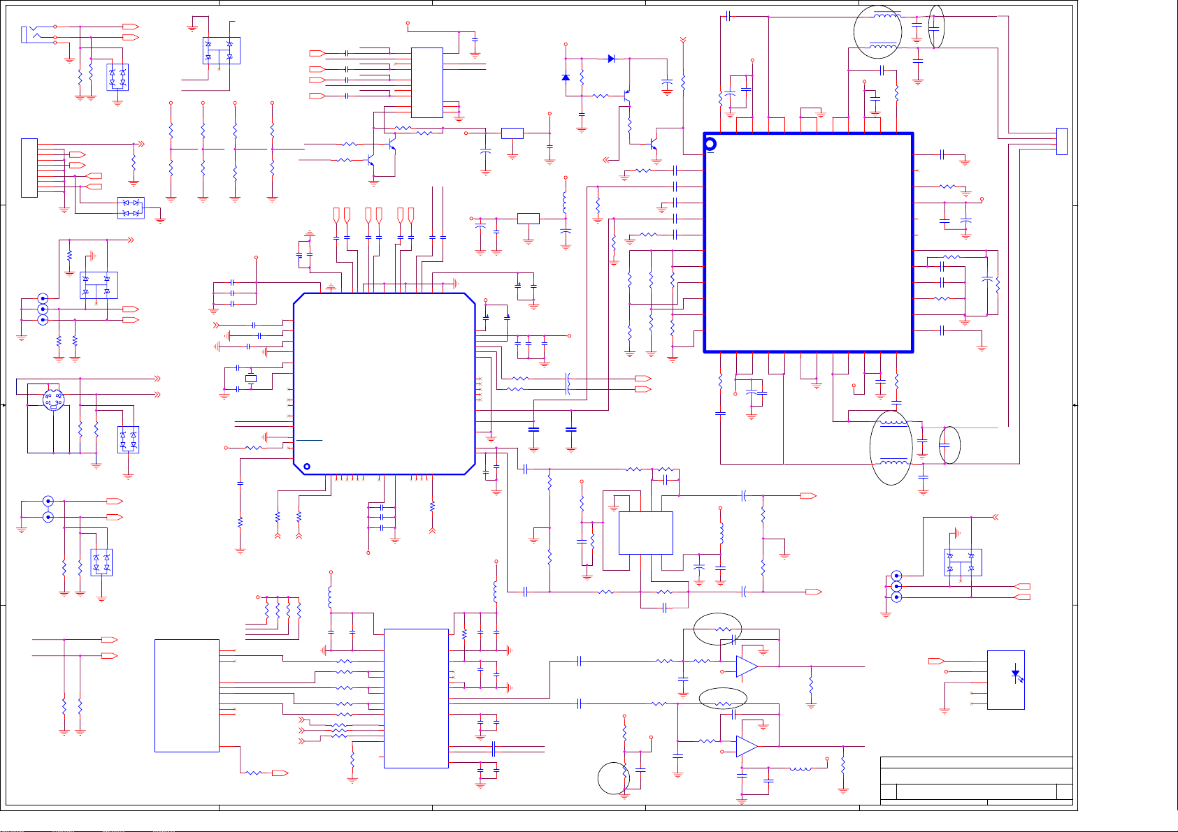
5
42
P201
1
2
3
EARPHONE
EAR-005
D D
CN201
1
2
3
4
5
6
7
8
9
10
CON10
CN-PH-10A
R209
R208
10K
10K
AV2_L
AV2_R
FROM SIDE AV_BOARD
RE-0805
R212
75
5
5
CONNECTOR COAX-J
P202
4
C C
5
6
RCA-009-XX4
R210
P203
Y
4
1
S-PORT
SVI-008
P204
B B
4
RJ-1087
RCA-123
A A
1
2
3
6 7
67
4
1
5
5
10K
10K
231
R215
R217
10K
C
2
2
3
3
10K
1234
123 4
R211
10K
R214
R213
75
RE-0805
RE-0805
2
R216
10K
R218
VGA_R
VGA_L
PESD5V0S2BT
1
2
1
2
DI-SOT23
3
ESD201
3
To video
switch 331
PHONE_L
PHONE_R
ESD205
1
1
2
2
PESD5V0S2BT
DI-SOT23
ESD202
PESD5V0L4UG
DI-SOT353
AV2
R275
75
RE-0805
3
3
To video
AV1
switch 331
AV1_L
AV1_R
To video switch 331
1
2
ESD203
1
2
75
2
3
HD1_L
HD1_R
1
ESD204
1
DI-SOT23
3
PESD5V0S2BT
HD2_L
HD2_R
3
3
PESD5V0S2BT
DI-SOT23
A8V
R20020K
DC_SET1 DC_SET2
R20120K
From tuner
S_Y
S_C
U1G
ADATAI2_DDXLA
ADATAO0_DDXLG
ADATAO0_DDXRA
ADATAO0_DDXRB
AV2_L
AV2_R
SupraHD-680
5
AV2
5
ESD207
5
PESD5V0L4UG
DI-SOT353
1234
123 4
A8V A8V A8V
R20420K
R20220K
R20320K
R20520K
A5V
C221 0.1u
C222 10nF
C223 10uF
CA-1206
C224 56pF
SIF
A5V
C226 56pF
C227 3.3pF
Y1
C228
3.3pF
18.432MHz
QU-4.8T11.4W2P
AU_SEL_B
AU_SEL_A
R219
R220
10K
C225 56pF
10K
C229
2.2uF/10V
For 3410&ADC&TIME
3.3V
R234
10K
LRCK
BCK
ACLK
DATA_OUT
P4
ADATAI0
ADATAI1
ACLK
BCLK
LRCLK
IEC956
DATA_IN
U2
T1
ACLK
R2
BCK
R3
LRCK
P3
DATA_OUT
T2
N4
U1
V1
R238
0R
R20620K
DC_SET4DC_SET3
R20720K
C219
10uF
CA-1206
38mA max
U201
50
51
52
53
54
55
56
57
58
59
60
61
62
63
64
47
R20a
100
SCL0
R235
10K
I2S_C3
I2S_C2
I2S_C1
VGA_L
AV2_L
VGA_R
AV2_R
ANA_IN1+
ANA_IN1ANA_IN2+
TESTEN
XTAL_IN
XTAL_OUT
TP
AUD_CL_OUT
NC
NC
D_CTR_I/O_1
D_CTR_I/O_0
ADR_SEL
STANDBYQ
NC
MONO_IN
100
R236
NC/10K
IEC9580
AU_SEL_B
AU_SEL_A
R21a
SDA0
R237
10K
4
C200
HD2_L
C201
C202
HD2_R
C203
C220
0.1u
48
49
AVSS
AVSUP
I2C_CL
I2C_DA
12345
3.3V
2
L208
120
1
CA-1206
R257 100
R258 100
R259 100
R260 100
R261 100
R276 100
R277 100
R278 100
4
R254 10K
DA_R
2.2uF
C211
46
I2S_CL
CO-0805
C289
10uF
DC_SET1
2.2uF
DC_SET2
DC_SET3
2.2uF
2.2uF
DC_SET4
2.2uF
R273 10K
BT3904
Q203
R272
10K
DA_L
2.2uF
C212
4544434241403938373635
VREFTOP
MSP3410G
I2S_WS
I2S_DA_OUT
6
C236
C234
C235 10uF
TR-SOT23-NPN
BT3904
Q202
HD1_L
HD1_R
2.2uF
2.2uF
C213
C214
ASG
ASG
SC1-IN-L
SC2-IN-L
SC1-IN-R
SC2-IN-R
SC3-IN-R
IC-MQFP64-1010-0.5
ADR_DA
ADR_WS
ADR_CL
DVSUP
I2S_DA_IN1
DVSS
789101112131415
10n
70mA
max
A5V
C290
U208
0.1uF
6 26
DVDD AVDD
7 25
DGND AGND
10
DOUT
28
ADCMCK
3
DACBCK
2
ADCBCK
5
DACLRC
4
ADCLRC
8
DIN
11
CSB/IDF
12
SCK/IWL
13
SDIN/DM
27
MODE
R255
14
MUTE
10K
WM8569
IC-SSOP28-307-0.65
A8V
U206
12
1Y0
VCC
14
1Y1
15
1Y2
1Z
11
1Y3
2Z
1
2Y0
5
4052
2Y1
2
2Y2
4
2Y3
10
S0
VEE
9
S1
GND
IC-SO16-245-50
R256 10K
AV1_L
AV1_R
PC_AV_R
2.2uF
2.2uF
2.2uF
C215
C216
C217
34
ASG
AGNDC
SC3-IN-L
SC4-IN-L
SC4-IN-R
I2S-DA-IN2NCNCNCRESETQ
16
100
0.1u
CA-1206
TU_RST#
Soft_reset for
353 and 3410
DACVRP
DACVRN
ADCVRN
OUTR
OUTL
VMID
REFADC
E
PC_AV_L
2.2uF
C218
33
R221
NCDACMCLK
NC
INR
INL
AHVSS
16
13
3
6
7
8
A8V
100uF/16V
CES-D6.3L5.5
A5V
C208
CES-D5L5.5
CAPL-M
AHVSUP
CAPL_A
SC1-OUT-L
SC1-OUT-R
VREF1
SC2-OUT-L
SC2-OUT-R
DACM_SUB
DACM_L
DACM_R
VREF2
DACA_L
DACA_R
18
241
9
17
16
23
22
19
20
21
15
PC_AV_L
PC_AV_R
C206
100uF
NC
NC
C238
R274
4.7
RE-0805
0.1u
C204
321
IC-DPAK
C209
3.3uF
CA-0805
A8V
C249
10uF
32
CA-1206
31
30
29
28
27
26
25
R222
24
23
22
21
20
19
18
17
1n
1n
C239
A5V
2
L209
120
CO-0805
1
C291
CA-1206
0.1uF
C293
0.1uF
CA-1206
C295
0.1uF
CA-1206
C299 2.2UF
C10 2.2UF
C297
CA-1206
0.1uF
U204
O
78M08
78M05
3
0.1uF
C251
C250
10uF
CA-1206
C246
470p
R223 100
100
C241 2.2UF
C292
10uF
C294
10uF
C296
10uF
C298
10uF
I
G
IC-DPAK
U205
O
C247
C242
C240
2.2UF
2
10n
1n
A_L
A_R
I
G
C248
A_L
A_R
3
D205
12V
1
C210
100uF/16V
CES-D6.3L5.5
C252
0.1U
8mA
max
2.2uF
C245 47uF
C244 47uF
R225OPEN
3
12V
1N4148
C207
0.1uF/16V
A8V
R224
OPEN
10K
2.2uF
C20
12V_DOWN
2
L201
120
CO-0805
1
A8V
1n
C243
A5V
R226
C254
2.2UF
C18 10UF
CA-1206
C19 10UF
CA-1206
D206
1N4148
R279
R280 20K
NC
R243
AUDIO_L
R229 6.8K
2K
2K
R227
R228 6.8K
R262
10K
R263
12K
R244
AUDIO_R
NC
R4
0
R1
A8V
CES-D5L5.5
C21
Q205
2N3906
R281
10K
3.3K
R290
R291
R3
NC
R2
0
NC
R230 8.2K
45
IC-SO8-225-50
R231 8.2K
C11
10u
CA-1206
100uF
BT3904
1u
1uF
3.3K
AV_OUT_L
AV_OUT_R
C255
A-A+V-B+
B OUTV+B-
786
C256
R265
10K
VR
R245
R264
10K
Q206
NC
123
A OUT
C2611uF
C262
C263
C264
C265
1uF
R246
NC
470p
U203
TDA1308T
470p
MUTE#
R239
1K
U202
1
2
3
4
1uF
5
6
7
8
9
10
11
12
CES-D5L5.5
R268
1K
C12
1000PF
C14
1000PF
CA-0603
R247
SD
RINN
RINP
V2P5
LINP
LINN
AVDDREF
NC
GAIN0
GAIN1
FAULT
NC
R249 0
C274
10nF
CA-0603
C257
100uF
VR
R269
1K
C268
10nF
C266
47uF/25V
CES-D6.3L5.5
+
0
47
48
BSRN
PVCCR
BSLN
PVCCL
13
14
18V
470uF/16v
A5V
CE-0500-D10L12
1
L226
120
CO-0805
2
0.1
C258
470uF
CE-0500-D10L12
R266
20K
C13 150PF
2
3
R267
20K
C15 150PF
6
5
C16
0.1UF
2
18V
C267
2.2uF/25V
CA-0805
45
46
PVCCR
ROUTN
PVCCL
LOUTN
1617181920
15
CES-D6.3L5.5
C275
C276
+
2.2uF/25V
CA-0805
47uF/25V
C259
C260
-
NJM4580E
1
+
IC-SO8-225-50
8 4
U209A
-
NJM4580E
7
+
U209B
IC-SO8-225-50
8 4
C17
10UF
CA-1206
2
44
ROUTN
TPA3008D2
IC-HTQFP48-0707-0.5
LOUTN
R232
10k
R233
10k
L210
CO-0805
43
PGNDR
PGNDL
33uH/2.5A
L204
SPI-D12.5L4.5
C271
0.1uF/25v
CA-0805
33uH/2.5A
L205
SPI-D12.5L4.5
C269 10nF
18V
2.2uF/25V
CA-0805
R248
0
C270
37
38
39
40
41
42
BSRP
PVCCR
PVCCR
ROUTP
ROUTP
PGNDR
PGNDL
PHONE_L
PHONE_R
R270
20K
A8VVR
120
12
PVCCL
LOUTP
LOUTP
21
22
18V
2.2uF/25V
L206
L207
33uH/2.5A
DA_R
DA_L
R271
20K
36
VCLAMPR
35
NC
34
NC
33
AVCC
0.1uF/25V
32
NC
CA-0805
31
NC
30
AGND
29
AVDD
28
COSC
R253 120K
27
ROSC
26
AGND
25
VCLAMPL
PVCCL
BSLP
24
23
R250
C277
0
RE-0603
CA-0805
C278
10nF
RE-0603
33uH/2.5A
SPI-D12.5L4.5
C280
0.1uF
CA-0805
SPI-D12.5L4.5
CONNECTOR COAX-J
P207
1
4
2
5
3
6
RCA-009-XX4
IEC9580
Title
AUDIO & ANA-INPUT
Size Document Number Rev
<Doc>
Date: Sheet of
CP-0500-5T7.5W
C273
0.33uF
C272
0.1uF/25v
CA-0805
C288
1uF/25V
CA-0805
R251
NC
C287 47uF/25V
C286
R252 NC
C284 1UF
C283 220pF
C282 1uF/25V
CA-0805
C281
0.33uF
CP-0500-5T7.5W
C279
0.1uF
CA-0805
AV_OUT_V
5
5
1234
123 4
5V
1
18V
+
CES-D6.3L5.5
C285
P206
1
扬声器端子
+
R5
0
NC
AV_OUT_V
ESD206
PESD5V0L4UG
DI-SOT353
(IEC 958 Audio Out)
IR Transmitter
1
Nin
2
Vcc
3
GND
4
NC1
5
NC2
GP1F32T
CN-0C1775203
CN202
R-
1
R+
2
L+
3
L-
4
AV_OUT_L
AV_OUT_R
27Saturday, March 31, 2007
C
Page 43

5
43
4
3
2
1
5V
D D
C C
From P1
TV
AV1
From P2
AV2
From P2
S_Y
CA-1206
CVBS_SEL0
CVBS_SEL1
B B
DAC Gain
R318
330R 1%
A A
R319
18R
5V 5V 5V
2.2uF
C301
DC1
C305
C306
C307 10uF
CA-1206
10uF
C308
R3016.8K
R3058.2k
R3096.8K
10uF
DC3
DC4
R3006.8K
R3048.2k
R3086.8K
U1J
SupraHD-680
H20
RSET
2.2uF
C302
DC2
CA-1206
10uF
CA-1206
R313 100
AVID_COMP
5
DC2
AVID_PR
AVID_Y
AVID_PB
R3026.8K
R3068.2k
R3106.8K
DC1
R312100
C303
DC3
2.2uF
J19
J18
J20
K18
R3036.8K
2.2uF
R3078.2k
C304
DC4
R3116.8K
U301
Video Switch
6
1B1
5
1B2
4
1B3
3
1B4
10
2B1
11
2B2
12
2B3
13
2B4
14
S0
2
S1
1
OE1
15
OE2
FSAV331MTC16
IC-QSOP16-225-0.65
RED_PR_C
R320
39R
RE-0805
R321
RE-0805
R322
RE-0805
220R
39R
39R
GRN_Y_Y
BLU_PB_0
COMP_OUT
VCC
GND
C331
1A
2A
R325
220R
5V
7
9
16
8
220uF
Q300
R325A
22pF
C330
S_C
2.2uF
C309
CES-D5L5.5
AV_OUT_V
CES-D6.3L5.
2N3906
TR-SOT23-PNP
R324
L301
1.8uH
CO-0805
270pF
R323 75R
C314
C310
47uF
Y
NC
5V
5
75
RE-0805
C329
330pF
C328
RE-0805
C313
1uF
4
C312
1uF
R314
C311
0.1uF
4.7R
R316
51R
C316
47pF
R317
NC
C317
47pF
C324
0.1uF
AV_OUT_V
?NC
R315
51R
C315
47pF
47uF
CES-D5L5.5
C320
47uF
CES-D5L5.5
VFE_VREFP
C327
10uF
CA-1206
0.1uF
C326
to P2
VFE_YIN
VFE_IBEXT
C318
+
CES-D5L5.5
VFE_CIN
VFE_VBG
C319
+
47uF
+
C325
0.1uF
VFE_VREFN
C322
0.1uF
C323
C321
0.1uF
0.1uF
W2
U4
Y3
U5
V3
W3
Y2
V4
VFE_YIN
VFE_IBEXT
VFE_CIN
VFE_VBG
SupraHD-680
VFE_CVBS
VFE_VCM
VFE_VREFP
VFE_VREFN
3
U1I
P301
TMDSD0+
TMDSD0-
TMDSD1+
TMDSD1-
TMDSD2+
TMDSD2-
TMDSC+
TMDSC-
DSHLD0
DSHLD1
DSHLD2
CSHLD0
DDC_GND
SHLD0
SHLD1
SHLD2
SHLD3
HDMI_CONN
HDI-002
CBL_5V
C332
0.1uF
DDC_SCL
DDC_SDA
改接
5v
SCL
SDA
CEC
HPD
VCC5
7
9
4
6
1
3
10
12
15
16
13
19
18
14
NC
2
5
8
11
17
20
21
22
23
6.8K
R326
CBL_HPD
R338
2.2
R327
6.8K
D0P
D0N
D1P
D1N
D2P
D2N
CLKP
CLKN
DDC_SCL
DDC_SDA
R337
NC
5V 5V
1uf
2
C338
D301
3
1
2
R339
NC
CBL_5V
3
2SK2158
3 1
2SK2158
HDMI_CEC
R336
1K
Q304
BT3904
TR-SOT23-NPN
2
D302
DI-SOT23
BAV99L
1
Q301
3 1
2
Q302
TR-SOT23-NFET
2
R335
Q303
BT3904
TR-SOT23-NPN
3.3V
TR-SOT23-NFET
3.3V
3.3V
R328
6.8K
220
R332
3.3K
R333
330
R329
6.8K
HDMI_SCL
HDMI_SCL
HDMI_SDA
HDMI_HPD
R331
R330
4.7K
HDMI_SDA
R334
390R
TP27
HDMI_VDD
4.7K
D2P
D2N D1N
Title
VIDEO & HDMI
Size Document
Sheet
Saturday, March 31, 2007
Date:
Drawn by:
U1D
SupraHD-680
D1
HDMI_D0P
E3
HDMI_D0N
F3
HDMI_D1P
E2
HDMI_D1N
F2
HDMI_D2P
E1
HDMI_D2N
D2
HDMI_CLKP
C1
HDMI_CLKN
C3
HDMI_SCL
B2
HDMI_SDA
B1
HDMI_CEC
A1
HDMI_HPD
D3
HDMI_REXT
R4
CTXI
C2
HDMI_RXATST
FCT
ESD301
1
1
6
2
2
5
3 4
34
PRTR5V0U4D
DI-SOT23-6
ESD302
D0P
1
1
2
2
D0N
3 4
34
PRTR5V0U4D
37
of
1
D1P
6
5
3.3V
6
6
5
5
DI-SOT23-6
Rev
C
CLKP
CLKN
3.3V
Page 44

5
44
U401
Digital GND
R423
0R
HD2_Y
HD2_Pb
HD2_Pr
R7R3R2
44
VPC7
TST0
5V
120
L400
CO-0805
C400
220uF
D D
C C
B B
AV-PORT3
A A
CES-D6.3L5.5
V33A
C417
C418
C419
10uF
10uF
G
G
2
G
2
CA-1206
10nF
C432
10nF
C436
10nF
C443
R419 10
S
1
1
S
3
3
S
2
4
6
8
10
0.1u
10nF
C431
10nF
C435
HD2_Y
HD1_Y
10nF
C442
R430
75
RE-0805
RE-0805
CN402
CA-1206
HD2_Pb
VGA_B
HD1_Pb TDVS
HD2_Y
VGA_G
HD1_Y
HD2_Pr
VGA_R
HD1_Pr
1.8V
P400
RCA-109
7 4
74
8 5
85
9 6
96
from USB
CN-PHD-14A
U400
C420
0.1u
10nF
C430
10nF
C434
10nF
C441
R431
75
RE-0805
1
3
5
7
9
C414
0.1uF
C421
C422
0.1u
0.1u
10nF
C437
10nF
C439
L404
120
CO-0805
CES-D5L5.5
R432
75
LT117-3.3V
3
I
IC-SOT223
C423
0.1u
R400
39R
R406
39R
39R
R412
C444
47uF
ESD400
1
1
2
2
3 4
34
PESD5V0L4UG
HD2_R
HD2_L
5
O
G
1
C425
C424
0.1u
0.1u
C429
0.01uF
R405 12K
0.01uF
C440
+
C446
10uF
CA-1206
HD1_Y
HD1_Pb
HD1_Pr
5
DI-SOT353
2
C433
0.01uF
5
CES-D6.3L5.5
C426
0.1u
0.01uF
C438
2mA
C445
RE-0805
C402 220uF
C427
C428
0.1u
0.1u
V33A
V33A
V33A
V33A
V33A
V33A
V33A
V33A
V33A
V33A
0.1uF
R447
75
RE-0805
301mA
+
R448
75
RE-0805
C415
0.1uF
V33D
45
VDDO6(33)
46
OGND6
47
AGND1
48
VDDA1(33)
49
REFB/PB
50
B/PB3
51
B/PB2
52
B/PB1
53
AGND2
54
VDDA2(33)
55
ANGDB/PB
56
BIAS
57
AGNDBIAS
58
AGND3
59
VDDA3(33)
60
AGND4
61
VDDA4(33)
62
REFG/Y
63
G/Y3
64
G/Y2
65
G/Y1
66
AGND5
67
VDDA5(33)
68
AGNDG/Y
69
VDDA6(33)
70
AGND6
71
AGNDSOG/Y
72
SOG/Y3
73
SOG/Y2
74
SOG/Y1
75
AGND7
76
VDDA7(33)
77
REFR/PR
78
R/PR3
79
R/PR2
80
R/PR1
81
AGND8
82
VDDA8(33)
83
AGNDR/PR
84
AGND9
85
VDDA9(33)
86
AGNDPLL
87
VDDA10(18)
88
VDDA11(33)
For 3410&ADC&TIME
R449
75
V33A
R6
R5
VPC6
TST1
VGA_HS
VGA_VS
SDA0
R4
VPC5
TST2
VPC4
TST3
VPC3
VPC2
OGND5
SCL0
4
R0
R1
V33D
NC
VPC0
VPC1
VDDO5(33)
TST6
TST5
TST4A0NCOEPD
100
9998979695949392919089
R426 100R
R427 100R
SDA0
SCL0
4
G7
G3
G6
G5
G4
V33D
NC
VPB4
VPB5
VPB6
VPB7
OGND4
VDDO4(33)
TDA8759
IC-QFP176-EP-2424-0.5
VSYNC2
VSYNC1
CLAMP
GAIN
COAST
TST8
TST7
107
106
105
104
103
102
101
R433
R435 100R
ESD402
1
1
5
2
2
3 4
34
PESD5V0L4UG
DI-SOT353
G2
G1
VPB2
VPB3
H(C)SYNC1
VSYNC3
109
108
5
G0
VPB0
VPB1
H(C)SYNC3
H(C)SYNC2
110
100R
C470
OGND3
CLEXT
111
V33D
NC
VDDO3(33)
TCLK
TST9
114
113
112
15
14
13
12
11
C459
22p
B7
NC
VPA7
115
nc
VGA-IN
B6
B5
VPA6
VDDC2(18)NCDIS
116
V18D
C471
P402
15
14
13
12
11
C460
B4
VPA5
CGND2
117
22p
VPA4
SDA
119
118
nc
5
10
4
9
3
8
2
7
1
6
VGA-001
V33D
OGND2
VDDO2(33)
IGND1
SCL
120
5
10
4
9
3
8
2
7
1
6
VGA_HS
VGA_VS
V18D
CGND1
TST10
122
121
R437
3K3
B3
B2
VPA3
VDDC1(18)
VDDI1(33)
TST11
124
123
V33D
DDC_W#
B1
VPA2
TST12
125
B0
VPA1
TST13
VPA0
IGND2
126
R436
3K3
NC
IGND3
127
C457
NC
128
GND1
130
129
CA-0805
4.7u
R444
RE-0805
V33D
12345678910111213141516171819202122232425262728293031323334353637383940414243
VCLK
HREF
VDDO1(33)
VDDC4(18)
IGND4
VDDC3(18)NCNC
132
131
V18D
V18D
DDC_W#
75
RE-0805
3
1
R445
3
add
R460
3K3
D400
75
VDDO7(33)
VDDC5(18)
3
DI-SOT23
RE-0805
VREF
FREF
ORG/Y
ORB/U
ORR/V
OGND7
TST17
TST16
TST15
TST14
CGND3
VDDI6(33)
DGND8
VDDI5(33)
IGND7
VDDI4(33)
IGND6
VDDI3(33)
VDDI2(33)
IGND5
6
7
8
24LC02
C456
0.1u
BAV70L
R446
75
VAI
CS
VS
HS
DE
PL
NC
NC
NC
NC
NC
NC
NC
NC
NC
NC
NC
NC
NC
NC
NC
NC
U402
SCL
VCLK
VCC
2
VGA_B
VGA_G
VGA_R
VGA_B
3.3V
176
175
174
173
172
171
170
169
168
167
166
165
164
163
162
161
160
159
158
157
156
155
154
153
152
151
150
149
148
147
146
145
144
143
142
141
140
139
138
137
136
135
134
133
VSSSDA
NC
NC
NC
IC-SO8-225-50
5v
L402
120
C401
CO-0805
CA-1206
TDCLK
4.7K
R404
TDHS
TDEN
V33D
V18D
V33D
V33D
V33D
V33D
V33D
55mA
45
3
2
1
ESD403
1
1
5
2
2
3 4
34
PESD5V0L4UG
DI-SOT353
V33D
C403
10uF
0.1u
TDCLK
TDVS
TDEN
C447
0.1u
3.3V 3.3V
VGA_R
5
VGA_G
V33D
26mA
C404
C405
0.1u
0.1u
B0
B1
B2
B3
B4
B5
B6
B7
G0
G1
G2
G3
G4
G5
G6
G7
R0
R1
R2
R3
R4
R5
R6
R7
M_BKLIGHT
R410 22
R413 22
R414 22
R415 22
V18D
C449
C448
0.1u
0.1u
R450
OPEN
RPF
R451
NC
C406
0.1u
RN400
RN401
RN402
RN403
RN404
RN405
C450
0.1u
C407
0.1u
22
22
22
22
22
22
R407 1K
R408
C451
0.1u
R452
OPEN
R453
1K
2
C409
C408
0.1u
0.1u
SRA0603X4
12
34
56
78
12
34
56
78
12
34
56
78
12
34
56
78
12
34
56
78
12
34
56
78
NC
PCLK
DHSTDHS
DVS
DEN
R416
4.7K
3.3V
C452
C453
10uF
0.1uF
NSB
BK_LIGHT_ON#
2
C410
0.1u
L20
L19
L18
L17
M20
M19
M18
M17
N20
N19
N18
N17
N16
P20
P19
P18
P17
P16
R19
R20
T19
R18
R17
T20
K20
K19
K17
U19
U20
T18
L405
120
CO-0805
M_BKLIGHT
C412
C411
0.1u
0.1u
U1F
/AFPIXIN0
/AFPIXIN1
/AFPIXIN2
/AFPIXIN3
/AFPIXIN4
/AFPIXIN5
/AFPIXIN6
/AFPIXIN7
/AFPIXIN8
/AFPIXIN9
/AFPIXIN10
/AFPIXIN11
/AFPIXIN12
/AFPIXIN13
/AFPIXIN14
/AFPIXIN15
/AFPIXIN16
/AFPIXIN17
/AFPIXIN18
/AFPIXIN19
/AFPIXIN20
/AFPIXIN21
/AFPIXIN22
/AFPIXIN23
HSYNC/PWM2
VSYNC
PCLK
DHSO
DVSO
DEN
C455
2.2uF
5V
12V
C413
C461
0.1u
0.1u
47UH
L403
PP_ON
SupraHD-680
LVDS_CK_P
LVDS_CK_N
LVDS_D1_P
LVDS_D1_N
LVDS_D3_P
LVDS_D3_N
LVDS_D0_P
LVDS_D0_N
LVDS_D2_P
LVDS_D2_N
LVDS_D4_N
LVDS_D4_P
LVDS_D5_N
LVDS_D5_P
LVDS_D6_N
LVDS_D6_P
LVDS_D7_N
LVDS_D7_P
LVDS_TXATST
LVDS_REXT
1.8V
P_BKLIGHT
C466
0.1uF
R442
1
20K
PP_ON
C454
0.1uF
5V
R439
10K
BKLT_EN
3
Q401
MMBT3904L
2
TR-SOT23-NPN
1
C462
CA4
10uF
+
CA-1206
C464
0.1uF
R402
20k
1
R4032k
3 2
B20
C19
C20
D19
D20
E19
E18
F17
F18
G17
F19
E20
G18
H18
G19
F20
H19
G20
E17
D18
FCT
R418
TP31
820R
470uF/16V
Q403
1
2
3
4
IC-SO8-225-50
Q404
2N3904
TR-SOT23-NPN
NSB
RPF
LVDS_D1_P
LVDS_D1_N
LVDS_D0_P
LVDS_D0_N
CMO use 50/60&RPF; LPL use
DCR_EN
&M_BKLIGHT&P_BKLIGHT&NSB
CMO use M_BKLIGHT; LPL use
P_BKLIGHT
D1
S1
D1
G1
D2
S2
D2
G2
AO4803
LVDS_CK_P
LVDS_CK_N
LVDS_D3_P
LVDS_D3_N
LVDS_D2_P
LVDS_D2_N
50/60
DCR_EN
8
7
6
5
+
10uF
470uF/16V
CA5
C463
P_5V
CN400
2
4
6
8
10
12
14
16
18
20
22
24
26
28
30
CONN EDGE 15X2
5V
R417
NC
FORMAT
R420
nc
P_12V
P_BKLIGHT
M_BKLIGHT
1
3
5
7
9
11
13
15
17
19
21
23
25
27
29
P_5V P_12V
CN401
1
2
3
4
CON4
of
:CN403/CN400
CN403
1 2
3 4
5 6
CON6A
Rev
1.8V
C
C458
0.1uF
5V
R438
OPEN
R441
OPEN
Title
ADC & LVDS & PANEL
Size Document
Sheet
Saturday, March 31, 2007
Date:
Drawn by:
画质增强接口
SDA0
SCL0
RSTn
47
1
Page 45
5
45
U1E
SupraHD-680
D D
C C
B B
GPIO3-GPIO0 = "1110" : Fixed boot from 8-bit NOR Flash
PP_ON
UART0RX
UART0TX
UART1TX
UART1RX
TPBIAS0
TPA0_N
TPA0
TPB0_N
TPB0
TPBIAS1
TPA1_N
TPA1
TPB1_N
TPB1
1394_RSET
I2C0CLK
I2C0DAT
I2C1CLK
I2C1DAT
CRXI
DRXI
TRSTN
TCLK
TAPSEL
GPIO0
GPIO1
GPIO2
GPIO3
GIRQ0
GIRQ1
GIRQ2
GIRQ3
GCS_N1
GCS_N2
GCS_N3
GCS_N4
GCS_N5
RESETN
CLKIN
CLKOUT
R525
TDO
TMS
IRR
TDI
1K
L4
P1
N1
L3
M1
H2
G2
F1
G1
H3
J4
J1
H1
J3
J2
G3
SCL0
R1
SDA0
P2
M3
M2
W1
V2
K5
K2
K4
K3
L1
K1
W4
V5
U6
Y4
V9
W20
Y20
V19
Y19
U18
V18
W18
Y18
N5
M4
QU-4.8T11.4W2P
N3
C515
10pF
FLASH_WPN
STDBY
MP_ON
R562 100
RSTn
24.576MHz
R526
RXD
TXD
3.3V
R5102.2K
R5092.2K
TU_RST#
R524 4.7K
I2S_C1
I2S_C2
I2S_C3
CVBS_SEL0
CVBS_SEL1
2
X502
4.7K
C501 0.1uF
C507 0.1uF
NC/5.9K
R512
SCL0
For 3410&ADC&TIME
SDA0
SCL1
Only for 353
SDA1
Soft_reset for
353 and 3410
3.3V
PP_ON
FLASH_WPN
BK_LIGHT_ON#
SET
WM8569
Control video
switch 331
DCR_EN
50/60
R560 100
R563 10K
C516
10pF
3.3V3.3V3.3V
R549
2K
STDBYBK_LIGHT_ON#
12 13
11
10
4
5
R561 10K
R550
4.7K
U509
ROUT1 RIN1
RIN2ROUT2
TIN1
T1OUT
TOUT2
TIN2
C2P
C2M
ST232C
IC-SO16-245-50
12V
0.1u/25V
+
CA2
470uF/16V
VCCC1P
VPC1M
VM
GND
R521 22R
CA-0805
5v
L506
120
CO-0805
TR-TO126-ECB
R544
C529
0.1uF
A A
L505
CO-0805
C530
100uF
CES-D5L5.5
120
C531
5V
LM1117DTX-3.3
U505
3 2
VIN VOUT
IC-SOT223
0.1uF
5
GND
TAB
1
4
320mA
C528 100uF
CES-D5L5.5
3.3V
+
161
23
89
14
7
6
15
R514
4.7K
C517
U503
8
SS/SD
C525
0.1u
IRU3037ACS
7
Comp
C527
2200p
R538
20k
Q500 2SB772
R545
470
470
BT3904
TR-SOT23-NPN
4
C509
0.1uF
2
VCC
4
IC-SO8-225-50
R546
470
Q503
4
GND
6
C539
0.1u
R515 1K
VC
HDrv
LDrv
Fb
C505
0.1uF
R516 1K
ESD501
5
5
PESD5V0L4UG
DI-SOT353
D504
LL4148
DI-SOD80
D506
C519
1u/25V
CA-0805
5
3
1
R548
5V
C503
0.1uF
RX
TX
R517
1K
1K
34
34
2
2
1
1
LL4148
DI-SOD80
R532 10
R534 10
R537
330/1%
U506
C540
220u
CES-D6.3L5.5
1K
ZD1
5.6V
ZN-SOD80
3.3V
R518
R519
NC
JTAG_RSTN
D505
LL4148
DI-SOD80
AMS1084-ADJ/25
tab/out
outin
gnd
IC-D2PAK
1
2.5V_ON
5V
L501
ZN-SOD80
JTAG/EJTAG
TRSTN
TDI
TDO
TMS
TCK
TMS
ZD3
5.6V
ZN-SOD80
C518
0.1u/25V
EPG1
EPG2
R535 1.8k/1%
4
32
CES-D6.3L5.5
120
CO-0805
ZD2
5.6V
CN505
46-35016W-14X
CN-DBD-14A
12V
L500
C520
0.1u/25V
CA-0805
MAX:670mA
C541
220u
190mA+240mA*2
P500
1
1
2
2
3
3
4
4
5
5
RS232
VGA-008
12
34
56
78
910
1112
1314
DC-DC 5V
15uH
SLF-D10L4.5
CA3
470uF/16V
CE-0500-D10L12
2.5V
C542
0.1u
6
7
8
9
C543
CA-1206
+
6
7
8
9
10u
IR_IN
3.3V
C546
1u/25V
CA-0805
5v
3
R506
* Key Pin 12
U504
8
d1
7
d1
6
d2
D13N03
L507
120
CO-0805
CES-D6.3L5.5
R540 3K
C535
5v
R556 10K
3
MISC
100
IR
STDBY
SDA0
SCL0
1
s1
2
g1
3
s2
45
g2d2
IC-SO8-225-50
220u
C532
0.15u
C506
27P
R551
C533
C508
27P
R123
EPG1
EPG2
add
0.1u
原来为
X500
8M
QU-4.8T11.4W2P
1K
C558
3.3V
R520
4K7
Q501
2SK2158
R527
4K7
Q502
2SK2158
U507
9
10
0.1u
IC-SO8-225-50
C560
C544
R547
IR_OUT
10n
100
R522
3K3
2
TR-SOT23-NFET
3.3V
R528
3K3
2
TR-SOT23-NFET
1 2
C521
470p
R533B
10
R533
10
EN
SS
MP1411
GNDFBCOMP
678
100p
10K
33P
MRS
5VS
R523
3K3
31
31
L502
10uH
SLF-D12.5L8
R533A
10
R533C
10
24
BSIN
SW
C545
10n
R500
15
16
5VS
5
10K
C504
0.1u
U500
4
8
6
3
5
PIC16F716
IC-SO18-407-50
R529
3K3
1920mA+PANEL
MCLR
OSC2
OSC1
B2/T1O
B0/INT
A4/T0
Vss
AN3/A3
AN2/A2
AN1/A1
AN0/A0
PWD/B7
PWB/B5
PWA/B3
M_SDA
M_SCL
12V_DOWN
add
R581
10K
CE-0500-D10L12
+
470uF/16V
C534
10n
VDD
INT/B6
T1/B1
R580
10K
5VS
C522
L503
SLF-D10L4.5
D508
R542
FM5817
DI-DO214AC
R543
2
5VS
CES-D5L5.5
B4
I/O:20mA
C512
0.1u
CA-0603
C523
0.1u
15uH
R541
? 1%
? 1%
? 1%
2
14
2
1
18
17
13
11
10
9
12
7
100u
C502
DOWN
5V
C500
0.1u
UP
R507
R508
MUTE#
U501
8
VCC
6
SCL
5
/INT2
S35380A
U502
C514
C524
10u
CA-1206
Reset
Switch
C537
10u
CA-1206
3.3V
3
OSCOUTSDA
6
7
8
0.1u
3.3V
C524A
10u
CA-1206
1.8V
C547
0.1u
R505
100
100
RE-0603
C511
5VS
1
D501
BAV70L
DI-SOT23
2
/INT1
OSCIN
GND
IC-SO8-225-50
SCL
24C16
TEST
VCC
3
1
4
DS1233A
IC-SOT223
JTAG_RSTN
950mA
C548
10u
CA-1206
R501
C556
0.1u
100
M_SDA
M_SCL
5VS
R511
2K
47p
BAT1
1 2
BATTER
X501
1
27
3
4
GNDSDA
A2
A1
A0
IC-SO8-225-50
U508
Reset Ckt
VCC
/RESET
GND
GND
SW1
1 2
SWKEY-YM061
SW-TAC001
R539 0
C538
C536
220u
CES-D6.3L5.5
0.1u
1K
R503
R504
C557
0.1u
C510
0.1u
CA-0603
D500 FM5817
R513
NC
1
D509
1
D510
32.768KHZ
QU-3.12D2P
45
3
2
1
2
C513
18p
3
3
KEY
1K
1K
C550
C554
3.3V
5V
1u
2
2
C526
10n
1
MRS
DOWN
UP
LED_R
LED_B
C555
1u
1u
C551
LED_B
1u
IR
KEY
LED_R
1
2
3
4
5
6
7
C553
1u
5VS
PW_ON
C552
1u
12V
18V
+
C599
CE-0500-D10L16
R531
1K
R536
220
R570
470
IR_IN
Title
Size Document
Date:
Drawn by:
470uF/25V
D503
R530
220R
"Power In LED"
D507
Yellow
"Reset LED"
R569 1K
IR_EN
13
11
9
7
5
3
1
46-38605W-14X
CN-PHD-14A
MCU & MISC & POWER
Sheet
57
of
Saturday, March 31, 2007
1
CN4-20A
1
2
3
4
CN500
PW_ON
2.5V_ON
CN501
LED2
LED1
+5VS
GND
IR
GND
KEY
46-35199W-8X
CN-PH-8A
CN503
4
3
2
1
yellow
12
DI-0805
RSTn 2,4,6,8
12
DI-0805
CN504
14
12
10
8
6
4
2
5VS
CN502
46-35199W-3X
1
2
3
CN-PH-3A
4
3
2
1
46-33333W-04X
CN-VH-4AW
5VS
3.3V
MP_ON
Rev
C
TO Keyboard
TO Powerboard
Page 46
5
46
4
3
2
1
U1H
C623
0.1uF
C614
0.1uF
C626
0.1uF
C615
0.1uF
C619
0.1uF
190mA
2.5V
D D
3.3V
290mA
C610
10uF
CA-1206
C611
10uF
CA-1206
1.8V
C621
0.1uF
C601
CA-1206
C613
0.1uF
C622
0.1uF
10uF
C627
0.1uF
C606
0.1uF
C618
0.1uF
C607
0.1uF
1.8V
890mA
C660
0.1uF
C643
0.1uF
C654
0.1uF
C638
0.1uF
C651
0.1uF
0.1uF
C635
0.1uF
C663
C639
0.1uF
L604
CO-0805
C657
10u
CA-1206
C633
0.1uF
C637
10u
CA-1206
C642
10u
CA-1206
C650
10u
CA-1206
120
120
120
120
1.8V
5
120
C631
0.1uF
L600
CO-0805
L602
CO-0805
L603
CO-0805
L605
CO-0805
L606
CO-0805
120
C629
10u
C C
CA-1206
3.3V3.3V3.3V3.3V3.3V3.3V
B B
A A
C608
0.1uF
VCC_DAC
C644
0.1uF
HDMI_VDD
C655
0.1uF
C659
0.1uF
C609
0.1uF
C636
0.1uF
VFE_VDD
ADAC_VDD
HDMI_VDD
LVDS_VDD
2.5V
1.8V
PLL_VDD
C661
0.01uF
VCC_DAC
4
3.3V
T10
T11
T12
T13
R14
P14
N15
M16
E10
E11
E12
E13
E14
E15
E16
R10
R11
R12
R13
P13
N14
M15
K15
H15
G14
F10
F11
F12
F13
F14
G15
H16
F15
L16
L15
J15
J16
T8
T9
R8
P7
N6
M5
L5
E6
E7
E8
E9
R9
P8
N7
M6
L6
K6
J5
J6
H6
G7
F7
F8
F9
H5
G5
G6
R7
R6
R5
D5
E5
F6
P6
IVDD1
IVDD2
IVDD3
IVDD4
IVDD5
IVDD6
IVDD7
IVDD8
IVDD9
IVDD10
IVDD11
IVDD12
IVDD13
IVDD14
IVDD15
IVDD16
MVDD1
MVDD2
MVDD3
MVDD4
MVDD5
MVDD6
MVDD7
MVDD8
MVDD9
MVDD10
MVDD11
CVDD1
CVDD2
CVDD3
CVDD4
CVDD5
CVDD6
CVDD7
CVDD8
CVDD9
CVDD10
CVDD11
CVDD12
CVDD13
CVDD14
CVDD15
CVDD16
CVDD17
CVDD18
CVDD19
CVDD20
CVDD21
CVDD22
CVDD23
CVDD24
CVDD25
CVDD26
CVDD27
CVDD28
CVDD29
CVDD30
1394VDD0
1394VDD1
1394VDD2
VFE_VDD0
VFE_VDD1
DAC_VDD
ADAC_VDDO
HDMI_VDD0
HDMI_VDD1
HDMI_VDD2
LVDS_VDD0
LVDS_VDD1
LVDS_VDD2
PLL_VDD
P9
GND1
P10
GND2
P11
GND3
P12
GND4
N8
GND5
N9
GND6
N10
GND7
N11
GND8
N12
GND9
N13
GND10
M7
GND11
M8
GND12
M9
GND13
M10
GND14
M11
GND15
M12
GND16
M13
GND17
M14
GND18
L7
GND19
L8
GND20
L9
GND21
L10
GND22
L11
GND23
L12
GND24
L13
GND25
L14
GND26
K7
GND27
K8
GND28
K9
GND29
K10
GND30
K11
GND31
K12
GND32
K13
GND33
K14
GND34
J7
GND35
J8
GND36
J9
GND37
J10
GND38
J11
GND39
J12
GND40
J13
GND41
J14
GND42
H7
GND43
H8
GND44
H9
GND45
H10
GND46
H11
GND47
H12
GND48
H13
GND49
H14
GND50
G8
GND51
G9
GND52
G10
GND53
G11
GND54
G12
GND55
G13
GND56
SupraHD-680
PLL_VSS
H4
G4
F4
T7
T6
J17
K16
T5
D4
E4
F5
G16
H17
F16
P5
1394VSS0
1394VSS1
1394VSS2
VFE_VSS0
VFE_VSS1
DAC_VSS1
DAC_VSS2
ADAC_VSS
HDMI_VSS0
HDMI_VSS1
HDMI_VSS2
LVDS_VSS0
LVDS_VSS1
LVDS_VSS2
Power and Ground 1
3
U1A
GDAT15
GDAT14
GDAT13
GDAT12
GDAT11
GDAT10
GDAT9
GDAT8
GDAT7
GDAT6
GDAT5
GDAT4
GDAT3
GDAT2
GDAT1
GDAT0
GADR15
GADR14
GADR13
GADR12
GADR11
GADR10
GADR9
GADR8
GADR7
GADR6
GADR5
GADR4
GADR3
GADR2
GADR1
GADR0
GALE
GIORD_N
GIOWR_N
GDIR
GOE_N
GWE_N
GWS_ACK
GCS_N0
SupraHD-680
T15
P15
W15
Y15
V15
U15
R15
Y16
Y17
T16
V16
W16
U16
R16
W17
V17
V10
V8
Y8
Y11
W6
W5
Y7
V7
V11
Y12
W12
U12
W13
V13
U13
W14
T14
V6
W7
U17
Y6
Y9
Y13
W19
GDAT13
GDAT12
GDAT11
GDAT10
GDAT9
GDAT8
GDAT7
GDAT6
GDAT5
GDAT4
GDAT3
GDAT2
GDAT1
GDAT0
GADR15
GADR14
GADR13
GADR12
GADR11
GADR10
GADR9
GADR8
GADR7
GADR6
GADR5
GADR4
GADR3
GADR2
GADR1
GADR0
4.7K
R601
4.7K
R602
TP32
FCT
2
4.7K
R603
3.3V
RSTn
GCS_N0
GOE_N
R604
NC
FLASH_WPN
RSTn
GADR1
GADR2
GADR3
GADR4
GADR5
GADR6
GADR7
GADR8
GADR9
GADR10
GADR11
GADR12
GADR13
GADR14
GADR15
GWE_N
R605
NC
GDAT8
GDAT9
GDAT10
GDAT11
GDAT12
GDAT13
3.3V
R600
4.7K
U601
25
A0
24
A1
23
A2
22
A3
21
A4
20
A5
19
A6
18
A7
8
A8
7
A9
6
A10
5
A11
4
A12
3
A13
2
A14
1
A15
48
A16
17
A17
16
A18
9
A19
10
A20
26
CE
28
OE
11
WE
12
RESET
14
VPP/WP
47
BYTE
M29W320DB/S29GL032R4-R3
IC-TSOP48-787-0.5
3.3V
Title
Size Document
Date:
Drawn by:
DQ15/A-1
C645
10uF
CA-1206
660POWER & FLASH
Sheet
67
Saturday, March 31, 2007
DQ0
DQ1
DQ2
DQ3
DQ4
DQ5
DQ6
DQ7
DQ8
DQ9
DQ10
DQ11
DQ12
DQ13
DQ14
VDD
VSS
VSS
of
1
R/B
GDAT0
29
GDAT1
31
GDAT2
33
GDAT3
35
GDAT4
38
GDAT5
40
GDAT6
42
GDAT7
44
30
32
34
36
39
41
43
GADR0
45
15
3.3V
37
13
NC
27
46
C646
0.1uF
Rev
C
Page 47
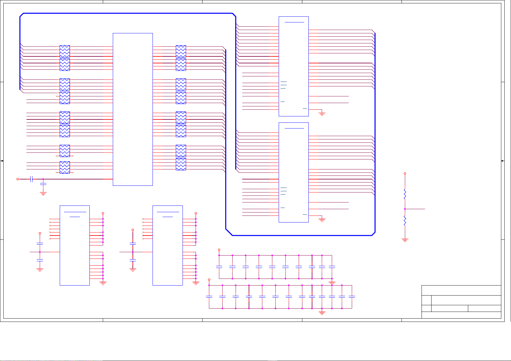
5
47
DDRA[0:12]
4
3
2
1
U701A
DDR SDRAM
DDRA12
DDRA11
C718
0.1uF
DDRBS1
DDRBS0
DDRRASN
DDRCASN
DDRWEN
DDRDM1
DDRDM0
DDRCKN
DDRCK
DDRCKE
DDRBS1
DDRBS0
DDRRASN
DDRCASN
DDRWEN
DDRDM3
DDRDM2
DDRCKN
DDRCK
DDRCKE
C708
0.1uF
C719
0.1uF
DDRA10
DDRA9
DDRA8
DDRA7
DDRA6
DDRA5
DDRA4
DDRA3
DDRA2
DDRA1
DDRA0
DDRA12
DDRA11
DDRA10
DDRA9
DDRA8
DDRA7
DDRA6
DDRA5
DDRA4
DDRA3
DDRA2
DDRA1
DDRA0
3
U1B
D D
C C
2.5V
B B
A A
DDRA0
DDRA1
DDRA2
DDRA3
DDRA4
DDRA5
DDRA6
DDRA7
DDRA8
DDRA9
DDRA10
DDRA11
DDRA12
DDRBS0
DDRBS1
DDRDQS0
DDRDQS1
DDRDQS2
DDRDQS3
DDRDM0
DDRDM1
DDRDM2
DDRDM3
DDRRASN
DDRCASN
DDRWEN
DDRCK
DDRCKN
DDRCKE
C700
0.1uF
RP706
RP707
22
RP700
22
RP701
22
RP702
22
RP703
22
RP704
22
RP705
22
22
C701
0.1uF
12
34
56
78
12
34
56
78
12
34
56
78
12
34
56
78
12
34
56
78
12
34
56
78
12
34
56
78
12
34
56
78
SRA0603X4
SRA0603X4
SRA0603X4
SRA0603X4
SRA0603X4
SRA0603X4
SRA0603X4
SRA0603X4
VREF
A2
SADR0
C12
SADR1
B3
SADR2
A11
SADR3
C11
SADR4
A20
SADR5
D11
SADR6
B19
SADR7
A10
SADR8
C18
SADR9
B12
SADR10
B10
SADR11
C10
SADR12
C4
SADR13
A12
SBS0
D6
SBS1
A5
SDQS0
D9
SDQS1
C14
SDQS2
D14
SDQS3
B7
SDQM0
A6
SDQM1
B15
SDQM2
A16
SDQM3
C5
SRASN
A19
SCASN
B4
SWEN
C17
SCK
B18
SCKN
D17
SCKE
B11
SVREF
SupraHD-680
U701B
DDR SDRAM
(PWR)
14
NC1
17
NC2
19
NC3
25
43
50
53
C702
0.1uF
49
C704
0.1uF
K4H561638F-TCB3-166
IC-TSOP66II-465-0.65
5
NC4
NC5
NC6
NC7
VREF
2.5V
VREF VREF
VDD1
VDD2
VDD3
VDDQ1
VDDQ2
VDDQ3
VDDQ4
VDDQ5
VSS1
VSS2
VSS3
VSSQ1
VSSQ2
VSSQ3
VSSQ4
VSSQ5
2.5V
1
18
33
3
9
15
55
61
34
48
66
6
12
52
58
64
240mA*2
2.5V
C703
0.1uF
SDATA0
SDATA1
SDATA2
SDATA3
SDATA4
SDATA5
SDATA6
SDATA7
SDATA8
SDATA9
SDATA10
SDATA11
SDATA12
SDATA13
SDATA14
SDATA15
SDATA16
SDATA17
SDATA18
SDATA19
SDATA20
SDATA21
SDATA22
SDATA23
SDATA24
SDATA25
SDATA26
SDATA27
SDATA28
SDATA29
SDATA30
SDATA31
U702B
C705
0.1uF
14
17
19
25
43
50
53
49
A4
B5
22
D8
RP708
C6
C7
D7
22
B6
RP709
A3
D10
C8
22
A9
RP710
B8
B9
A7
22
C9
RP711
A8
A14
B13
22
B14
RP712
C13
A15
D12
22
D13
RP713
A13
D16
C15
22
A18
RP714
B16
B17
A17
22
C16
RP715
D15
DDR SDRAM
(PWR)
NC1
NC2
NC3
NC4
NC5
NC6
NC7
VREF
K4H561638F-TCB3-166
IC-TSOP66II-465-0.65
4
VDD1
VDD2
VDD3
VDDQ1
VDDQ2
VDDQ3
VDDQ4
VDDQ5
VSS1
VSS2
VSS3
VSSQ1
VSSQ2
VSSQ3
VSSQ4
VSSQ5
12
34
56
78
12
34
56
78
12
34
56
78
12
34
56
78
12
34
56
78
12
34
56
78
12
34
56
78
12
34
56
78
1
18
33
3
9
15
55
61
34
48
66
6
12
52
58
64
SRA0603X4
SRA0603X4
SRA0603X4
SRA0603X4
SRA0603X4
SRA0603X4
SRA0603X4
SRA0603X4
2.5V
DDRDQ5
DDRDQ3
DDRDQ1
DDRDQ4
DDRDQ2
DDRDQ0
DDRDQ7
DDRDQ8
DDRDQ11
DDRDQ10
DDRDQ13
DDRDQ12
DDRDQ9
DDRDQ14
DDRDQ15
DDRDQ18
DDRDQ17
DDRDQ20
DDRDQ21
DDRDQ22
DDRDQ23
DDRDQ16
DDRDQ19
DDRDQ31
DDRDQ27
DDRDQ24
DDRDQ29
DDRDQ26
DDRDQ28
DDRDQ30
DDRDQ25
2.5V
C716
10uF
CA-1206
2.5V
C706
10uF
CA-1206
C717
10uF
CA-1206
C707
10uF
CA-1206
42
RES(A12)
41 2
A11 DQ0
28
A10
40
A9
39
A8
38
A7
37
A6
36
A5
35
A4
32
A3
31
A2
30
A1
29
A0
27
BA1
26
BA0
23
RAS
22
CAS
21
WE
47
UDM
20 51
LDM UDQS
46
CK
45
CK
K4H561638F-TCB3-166
IC-TSOP66II-465-0.65
U702A
42
RES(A12)
41 2
A11 DQ0
28
A10
40
A9
39
A8
38
A7
37
A6
36
A5
35
A4
32
A3
31
A2
30
A1
29
A0
27
BA1
26
BA0
23
RAS
22
CAS
21
WE
47
UDM
20 51
LDM UDQS
46
CK
45
CK
K4H561638F-TCB3-166
TSOPII66-430-0.65
C709
C710
0.1uF
0.1uF
C720
C721
0.1uF
0.1uF
LDQS
DDR SDRAM
LDQS
DDRDQ[0:31]
C711
0.1uF
C722
0.1uF
DQ1
DQ2
DQ3
DQ4
DQ5
DQ6
DQ7
DQ8
DQ9
DQ10
DQ11
DQ12
DQ13
DQ14
DQ15
DQ1
DQ2
DQ3
DQ4
DQ5
DQ6
DQ7
DQ8
DQ9
DQ10
DQ11
DQ12
DQ13
DQ14
DQ15
C712
0.1uF
CSCKE
CSCKE
C723
0.1uF
4
5
7
8
10
11
13
54
56
57
59
60
62
63
65
16
2444
(K4D551638F)
DDRDQ16
DDRDQ17
4
DDRDQ18
5
DDRDQ19
7
DDRDQ20
8
DDRDQ21
10
DDRDQ22
11
DDRDQ23
13
DDRDQ24
54
DDRDQ25
56
DDRDQ26
57
DDRDQ27
59
DDRDQ28
60
DDRDQ29
62
DDRDQ30
63
DDRDQ31
65
16
2444
(K4D551638F)
C714
C713
0.1uF
0.1uF
C725
C724
0.1uF
0.1uF
DDRDQ0
DDRDQ1
DDRDQ2
DDRDQ3
DDRDQ4
DDRDQ5
DDRDQ6
DDRDQ7DDRDQ6
DDRDQ8
DDRDQ9
DDRDQ10
DDRDQ11
DDRDQ12
DDRDQ13
DDRDQ14
DDRDQ15
DDRDQS1
DDRDQS0
240mAX2=480mA
DDRDQS3
DDRDQS2
C715
0.1uF
C726
C727
C728
0.1uF
0.1uF
0.1uF
2
2.5V
R700
VREF Generation
4.7K
VREF
R701
4.7K
DDR SDRAM Interface
Title
DDR
Size Document
Sheet
77
Saturday, March 31, 2007
Date:
Drawn by:
of
1
Rev
C
Page 48

7.power Supply
Service Principle
power supply board introduce
Using for model L32M61az and l42m61az power supply board
48
Page 49

01-MON37A-PW.sch-1 - Thu Nov 02 11:05:28 2006
49
Page 50

P
ower supply board
face
50
Page 51

power supply part schematic diagram
51
Page 52
power supply specification
VOLTAGE
(ACCURACY)
MAX
MAX
Input AC
90-265V
Standby power 0.5W
OUTPUT
+24VDC
+12VDC
+5VDC
TOLERANCE
OUTPUT CURRENT
MIN
±5.0% 0.8A 6A
(ACCURACY)
±8.0% 1.0A 4A
(ACCURACY)
5.0% 0.05A 0.5A
±
MIN
MIN MAX
52
Page 53

inputing circuit introduce
300V
The alternating current pass the common-mode circuit (making up of F801、RV801、C819、L806、LF802、LF801、R824 etc) when switching on the AC220v,
Choking back of sorts the alternating current EMC interfere, avoid the high frequency interfering pulse of the using voltage. Passing the BD801
commute,output 300v or not volts DC.
53
Page 54

Standby circuit introduce
320V
待机电路介绍
0V
320V
0.5V
1V
1V
When switching on ,at first the standby circuit work. Supply 5V to the figure board , the main power start working when receiving the figure board boot-strap
signal. Output: 24v、12v。300v volts d.c. pass the D810、R832,and then transformer(T803) primary coil,thereinto 3 pin connet pin 5、6、7 of U4 VDD、from
U4 source、drain put through,and so that the transformer(T803) primary coil put through ,telepathy secondary 9 pin outputing through D807 commute 5V
12V
2.5V
2.5V
1.2V
2.2V
54
Page 55

Standby voltage。R838 sampling 5v voltage,connect sampling 5V,connect to pin 1 ,TLHPC92 therepathy U3 pin 3、4 put through ,leave each other
Connect from the signal to U4 PIN 3、4,control U4 outputing ,and so that the transformer output the steady 5v 。
At the same time,the transformer T803 primary coil 4 pin divde into two-way outputting
1、 one-way output 15v to the VCC,supply to IC supplying power
2、 one-way output to U4 supply power。
Switch on/off work flow
Switch on
signal
13V
13V
13V
13V
9V
0.08V
55
Page 56

Switch on work flow
It passes R842、R841、D819 when receiving the figure board outputting the switch on high level signal ,and then senf to Q808 Base、Q808 break over 、TLU2 1、
2 pin break over、the signal coupling to TL U2 pin 3、4。At the same time Q807 cut off、TLU2 pin 1 、2 disconnection、not coupling the signal to TLU2 pin 3 、
4。At the same time Q807 cut off,15V cannot supply through the Q807 outputing the VCC,U5 and U6 stop working if they cannot receive the supply
power。
PFC circuit introduce
56
Page 57

4.7V
V oltage control
PFC
inductance
400V
Over current
protect
0V
6V
15V ingress and U6 startup,P7 OUTPUT CONTROLING Q801 CUT OFF AND BREAK OVER、L801 is energy storage constantly、commute the voltage
Upgrade the 380V or not , pass the C807 filter, outputting to PWM circuit.
0
V
0
V
1.8V
13.8V
CONTROLING Q801 CUT OFF AND BREAK OVER
PFC380V over voltage
protect samplying
0V
15V ingress and U6 startup,P7 OUTPUT
PWM circuit introduce
57
Page 58

15V
0.2V
0V
0.5V
400V
28V
Clampling
Avoid seep
inductance
bringing vol.
15V
0.08V
24V
0
0V
V
0.1V
0V
After 15v enter u5 pin P6, U5 start working, p5 output the pulse signal control Q805 and Q802 base、when the pulse signal is high level,Q805 cut off、
Q803 break over、VCC pass though the Q802 and R813 to charge up C820。when the pulse signal is low level,Q805 break over、Q803 cut off、C802 pass
though Q820 discharge 。 on account of C820 overlap cycle charge and discharge,on account of T802 secondary coil coupling to signal variety,and
so that control Q803 AND Q806 cut off and disconnect。In this way PFC Circuit output voltage conneting the transform T801 primary coil,also
repeat constantly deposited enery and released enery exchange course , and then telepathy to secondary coil and output voltage: 12v、24v
12V and 24V steady circuit
58
Page 59

13.5V
16V
2.4V
Pass through R811 sampling 24v and R808 sampling 12v,sampling the signal passing through U1 telepathy controling U5 PIN P2 ,adjust U5 PIN P5
Output the pulse width 、adjust T801 output
59
Page 60

over vo ltage protect circuit analyse
Fan-out 24v 12v
Over voltage range 28v—35v 14v—19v
60
Page 61
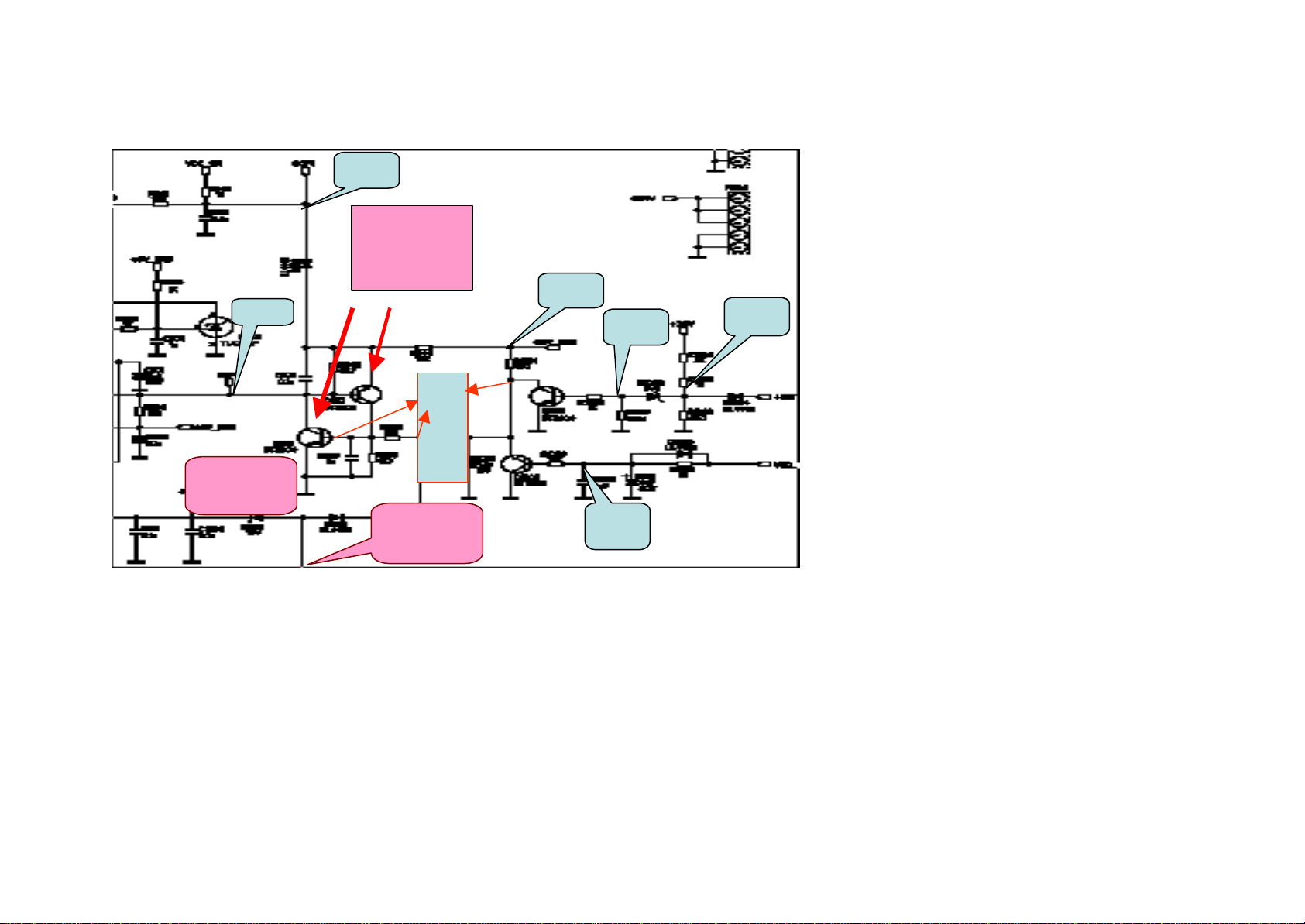
sampling
ork in gear
4.6V
0V
W
12V
When the voltage is over and sampling signal mix through D809、R856 , the high level send to Q812 base,at the same time Q810 collector is high level。
Q810 is break over、through D820 connect to R842,the potential alter low level ,the switch on signal high level can not operate,TV starts standby.
Q812、Q810
Cut off
24V
sampling
5V
5V
1V
10V
protect range
low-voltage protect circuit
61
Page 62

10V
1V
5V
When it is in gear about 24v , 24v through R1004、R1005、R1006 change the voltage,the Q1001 break-over,Q1001 collecter is lower level。
When the voltage is lower 24v, D1002 cannot break-over,Q1001 collecter is high level ,D1001 and Q812 break-over ,switch-on signal voltage change lower,
TV shift standby
service way
62
Page 63
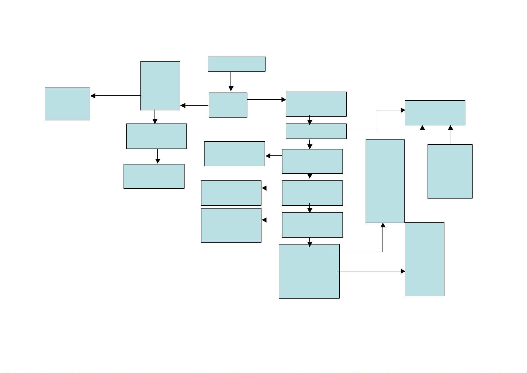
Detect
t U7 PIN
r current
and
ver current and
voltage protect
Y
isconnect
affirmover
inputing
filter circuit
N
Inspect
commute
bridge
outputing
N
no power supply
5V
voltage
Y
Supply switching
on voltage
Y
Detect protect
circuit
Practice cases1
Detect U4 P4
PIN voltage
Detect TL
feedfack circuit
Detect D824
Q807
Detect PFC
circuit
Detect PWM
TL feedback
circuit
N
N
N
Disconnnet D820
Detect 13V
voltage
Detect PFC
outputing
Y
Detect PWM
circuit
Detect 12V
24V
O
circuit
Disconne
ct U7
P7 pin
affirm
over
current
protectt
D
D1001
current
protect
Disconnec
P7
affirmove
protect
63
Page 64

Fault electrophoresis: no voltage
Analysis and detect: at first testing the switching on,p802 gain 2.2v switching on voltage in power board, constaint the power is on,testing 12v and 24v is
0v,measuring 5v is in gear。Showing the TV can standby in gear。If measuring 12v and 24v is 0V,the problem cause is 12v and 24v commonality part 。
12v and 24v commonality part is:PFC part and power PWN part 、over current and voltage protect part 。At first measure L809 PFC voltage。If it
discovering 380v is 0V,the problem is PFC,contact the PWM problem , primary analyzing cause is 15V circuit,U5 and U6 can not work when only 15V
has not in gear。
We know: the transformer T803 secondary coil 4 pin outpu t second part:
1. one way output 15V to VCC,supply to ic power supply
2. one way to U4 supply power,supply to 5VSTB
beause 5V is in gear,IC power supply is 15V,measure R826 VCC outputting voltage is 0V。measure R826 resistance to GND is in gear。And then
measuring Q807 transmit is not voltage。Measure D824,discovering one pin has voltage,measure D824,discover the D824 disconnection,replace
the D824,the voltage is ok!
Practice cases2
Fault electrophoresis: no voltage
Analysis and detect: at first testing the switching on,p802 gain 2.2v switching on voltage in power board, constaint the power is on,testing 12v and 24v is
0v,measuring 5v is in gear。Showing the TV can standby in gear。 Measuring 12v and 24v is 0V,the problem cause is 12v and 24v commonality part。
12v and 24v commonality part is:PFC part and power PWN part 、over current and voltage protect part 。At first is there 15V of VCC ,Is there Q807
T ransistor of 13V。U2 has not gain the switch on controling signal。 Disconnect D820,and than measuer ,now avoid the problem of over current and
voltage , the problem is the switch on signal has not effect。Constant switch on signal has inputted the P802, testing discover R842 disconnection,the
Switch on signal has not send to the Q808,replace R842,The TV switch on testing,the fault avoid。
Practice cases3
Fault electrophoresis: no voltage
Analysis and detect: at first testing the switching on,p802 gain 2.2v switching on voltage in power board, constaint the power is on,testing 12v and 24v is
0v,measuring 5v is in gear。Showing the TV can standby in gear。If measuring 12v and 24v is 0V,the problem cause is 12v and 24v commonality part 。
64
Page 65

12v and 24v commonality part is:PFC part and power PWN part 、over current and voltage protect part 。
At first disconnect D820 ,affirm where the problem is part,and then measure 13V of VCC,if it is in gear,continue testing PFC voltage is in gear,
So that determinant the problem is protect circuit,measuring D820 cathode to GND resistance,discovery resistance is littler than in gear ,testing
Protect circuit,discovery Q812 short circuit attaint。Replacing the Q812 ,the TV is ok!
Practice cases4
Fault electrophoresis: switch on voltage moment,12V testing point is 20V,24V testing point is 30V. 。fall to 0.4V or not moment .
Analysis and detect: at first testing the switching on,p802 gain 2.2v switching on voltage in power board, constaint the power is on,switch on voltage
moment,12V testing point is 20V,24V testing point is 30V. 。fall to 0.4V or not moment .measuring 5V is in gear,the TV can standby in gear,the problem
is 12V and 24V steadfast voltage pass from R811 sampling 24V and R808 sampling 12V,sampling signal pass though telepathy controlling U5 pin P5,
and then output the pulse width、adjust T801 outputting。
Detecting 12V and 24V steadfast voltage part,discovering Q804 is bad,replace it the fault aviod!
Practice cases5
Fault electrophoresis: when5V, dithering, and the output is 4V, no voltage at 12 V and 24V
Analysis, examine and repair: Open the panel and test, find out when5V, dithering, the output is 4V, and no output at other voltage, it means there is something wrong
with standby, it can’t export the stable 5V standby voltage.
At first, Check whether the commute bridge exports voltage: measure and find out there is 300 V direct current in D810, then check U4 to find out whether it starts
work, measure the start voltage of U4 at first. There is dithering in 11V, but 13V is normal, the matter is in support part of work voltage, measure pin 4 voltage
output of D803,there has voltage, measure D822, it is no voltage, then measure R847, find out there is plough, exchange it and eliminates the malfunction.
Practice cases6
Fault electrophoresis:: no voltage at 5V, 12 V and 24V.
Analysis, examine and repair: open the panel and test, there is no voltage, means the machine has something wrong with standby, it can’t output the 5V standby
65
Page 66

voltage, so it can’t produce 12V and 24V.
Check whether the commute bridge exports voltage: measure and find out there is 300V direct current in D810,then check U4 to find out whether it starts work,
measure the start voltage of U4 at first. There is dithering in 6-7V, but 13V is normal, measure 4 feet voltage output of D803, there has voltage, measure D822, it is
7V, find out no output when test D824,shows that it can’t run normally when at 5V , so exchange the U4, malfunction disappears.
Practice cases7
Fault electrophoresis:no voltage for 12V and 14V.
Analysis, examine and repair: open the machine and test at first, find out when standby at 5V voltage is normal means no problem with standby, provide the 2.2V
start voltage, no voltage output, so there is something wrong with the 12V and 14V voltage part, maybe the problem appears in PFC, PWM and protective circuit.
Measure the output voltage of VCC, 12V in R836, at this time there is noise in transformer, it is the voltage output reducing, maybe there is something wrong with
the protective circuit, then cut D820 of protective circuit, test again, there is normal voltage output, so it can conclude that the problem is in protective circuit, the
problem is over current and voltage or low-voltage 、low-current protect circuit。 Cut the protect point after connect the D820, voltage goes back to normal when
cuts the D1001, then test the low-voltage protect circuit , Q1001 is plough, exchange it and the malfunction disappears.
Practice cases8
Fault electrophoresis:the TV is no power supply
Analysis, examine and repair: check the machine first, find out the fuse is cut and no obvious component burned-out mark, circuitry has over current or voltage
circuit since the fuse is burned, means there is short circuit in somewhere. Measure and find out the Q801 has been short circuit, no short circuit finding in other
parts, exchange the Q801, test against, 5V voltage is normal, but no output at 12V 和 24V, because the PFC is broken, the voltage output of PFC is only about 320V,
PFC doesn’t run, the power supply voltage of PFC at 14V, it is normal, so decide to exchange U6, the malfunction is still here, measure each feet against floor
resistance of U6 in turn, find out the R869 is plough, exchange and test, eliminates malfunction, the fact is that R869 disconnect caused the U6 over current protect
circuit runs,U6 stop the output, so there is no voltage output of PFC, and no voltage.
Practice cases9
Fault electrophoresis:no voltage for 12V and 14V.
Analysis, examine and repair: open the panel and test at first, find out when standby at 5 V, the voltage is normal, means no problem with standby, then provide 2.2 V
66
Page 67

start volt age, make out no output at12V and 14V. The TV is standby.
Problem both at 12V and 14V voltage, maybe there is some matter with PFC, PWM and protective circuit, so measure output of PFC first, it is 320V, means PFC
doesn’t work, cut down the protective circuit, start the machine to test the output on 12V and 14V voltage, it is normal, so the problem appears in protective circuit,
cut down the over current protect point separately to test , malfunction still, then cut down the exceed press protect, malfunction still,too, cut down the
low-voltage protect Q1001 at last, malfunction disappears, and none of base voltage with Q1001, test and find out that 24V low-voltage protect sampling
resistance R1004 disconnection. Open the machine after exchange it, malfunction disappears.
Practice cases10
Fault electrophoresis:no voltage for 12V and 14V.
Analysis, examine and repair: open the panel and test at first, find out when standby at 5 V, the voltage is normal, means no problem with standby, then provide 2.2 V
start voltage, make out no output at 12V and 14V. The machine is standby, problem appears both at 12V and 14V voltage, maybe there is some matter with PFC,
PWM and protective circuit, so measure output of PFC first, if is 380 V, means PFC runs normally. It can conclude that problem is at 12V and 14V voltage part.
Since no voltage for both at 12V and 14V, the chance that feedback loop gets in trouble is not big, check the PWM circuit first, examine the going of U5, check
whether there is drive voltage of pin P5 on U5,dittering on 1.5V more or less is normal. Then measure against floor resistance of P5 on U5, cut down the outing
circuit, short circuit, it can conclude that U5 has been broken, open after exchange it, find out that the malfunction disappears.
Practice cases11
bake-machine maintenance attainment
1. Measure reverse resistance of commute bridge D801 :50O\infinite for positive.
2.Measure Q801stand of fall , measure positive resistance of D807 only, reverse resistance:70O.
3.Examine organization of D pole and S pole both D806 and Q803:50O.
4.Examine the foot against floor resistance of P4 and P6 on U6:0O.
5. Examine whether the resistance of R825 is infinite.
Remark: the metrical resistance above is measure data by using pointer multimeter on 10O
67
Page 68

7.Explode View Diagram
68
Page 69
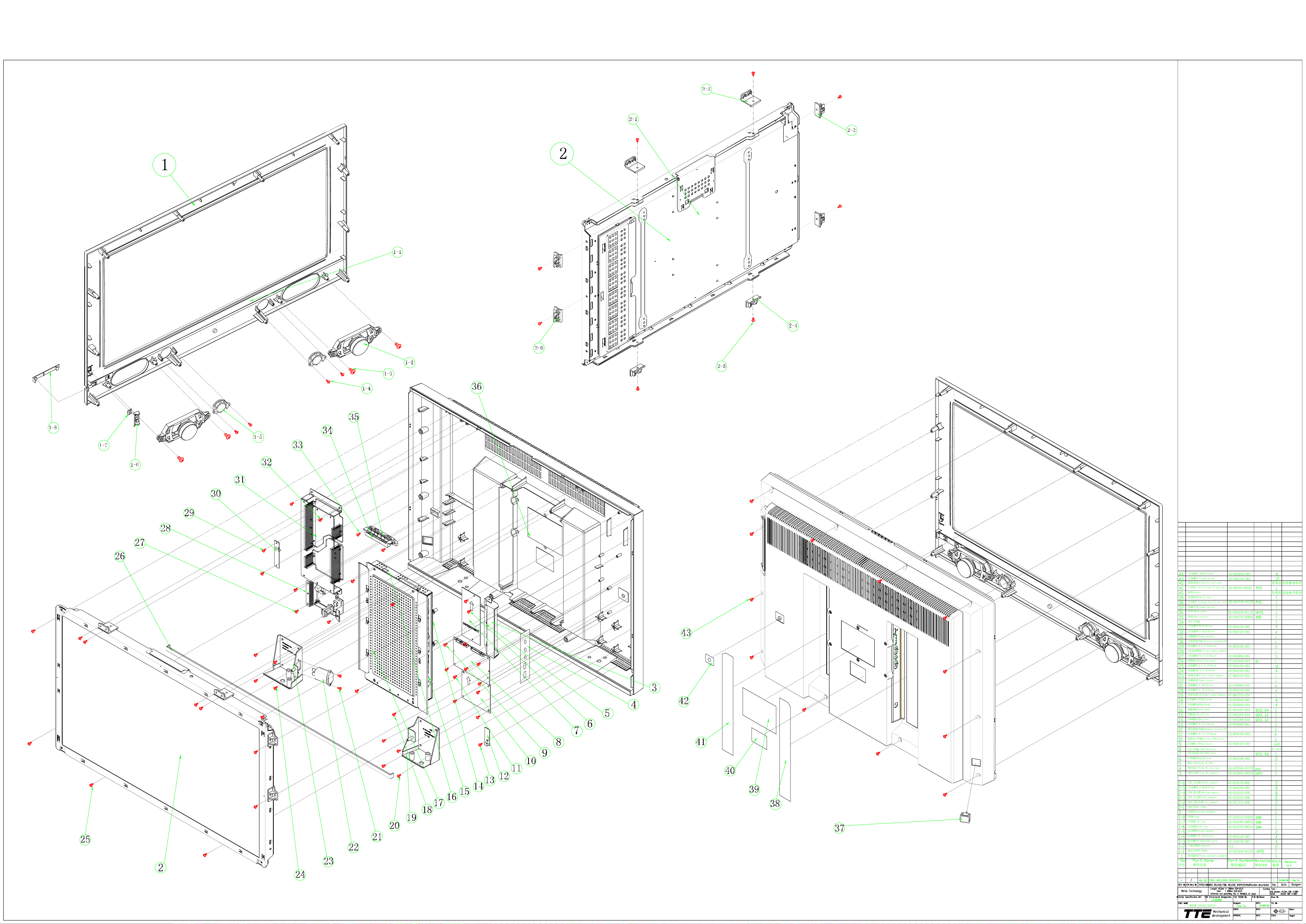
7.Explode View Diagram
8.Explode View Diagram
8.Explode View Diagram
8.Explode View Diagram
36
69
Page 70

9: Main IC Description
SupraHD-660-680-DTS-GEN-v1.7 -- Preliminary Release
9.1
Zoran ZR39660/680
13-39661B-GCB IC ZR39661BGC U1
• Embedded Processing Unit
• Integrated High-Performance MIPS® 4KEc™ CPU, 166
MHz
• Intended to run RTOS, audio decode and Application
software
• 32-bit MIPS32 enhanced architecture
• 8 K instruction cache, 8 K data cache, (2-way set
associative)
• MMU with 16-dual entry Joint Translation Lookaside
Buffer
• Two 32-bit Counter Timers for CPU timing functions
• One 32-bit Watchdog timer
• Integrated HDMI Link and PHY
• High-Performance MPEG-2 Video Decoding
Engine
• Transport Processing Unit with Integrated
CableCard support
• Uncompressed Digital Interface
• Accelerated 2-D Graphics
• Integrated PAL/NTSC Decoder
• 1394A High Speed Interface (Integrated Link and
PHY)
• Video Scaling and Format Conversion
• Display Processor & Controller
• Audio Processing Unit (APU)
• System Interfaces
• Two 2-signal UARTs
•Three I2C master or slave interfaces (up to 400 kb/s)
• One IR Receive, with hardware demodulation
• Guest bus interface
• Device Unique Chip ID
• 128-bit device unique secret key
• Memory Interface Unit
• High performance 32-bit DDR interface (200 MHz)
• Up to 1.3 GByte/second peak memory throughput
• 256 MByte memory address range
• Integrated Digital VCXO
• Process Technology
•0.18 u CMOS
•Power
• 1.8 V core voltage, 2.5 V Memory I/F, 3.3 V I/O
• Packaging
• 27 mm x 27 mm Plastic Ball Grid Array package
• 400 PBGA
Memory
Interface Unit
(MIF)
Audio
Processing Unit
(APU)
L/R
Audio
DACs
Display
Processor
(DPC )
Graphics
Video DACs
Video I/F
LVDS Output
MPEG2 Decode
Unit
(VDEC)
uController
(MCU)
Sequencer
(MCE)
NTSC/PAL
Encoder
BLT
CLKGEN
DVCXO
PLL
Link List
Unique 128-bit
ID
TS
1394
I/O
TS
Out
CNTL
TS
In
HDMI
In
NTSC
PAL
2 Pin
2 Pin
2 Pin
2 Pin
2 Pin
4 I/O
16 Bit
LB
JTAG
Ctlr.
1394
Phy
HDMI
PHY
Embedded
Processing Unit
(EPC)
MIPS 4Kec
I Cac he
D Cache
MMU
EJTAG
Ctlr.
Counters/
Timers
Transpor t
Processing Unit
(TRP)
Xport I/F
Descrambler
1394 Link
Xport Demux
CableCard
I/F
Video Capture
Unit
HDMI
NTSC/PAL
Decoder
Flex Bus Unit
(FBU)
UART0
UART1
I2C Ctlr. 1
I2C Ctlr. 2
I2C Ctlr. 3
GPIO
IRR
Guest Bus
ZR39680
Figure 1 SupraHD-680 IC Block Diagram
32
I2S I/O
L/R Out
Analog
Out
U
/
D
I
L
V
D
O
u
t
XTL
O
S
1 CONFIDENTIAL INFORMATION-DO NOT COPY 7/12/05
70
Page 71

SupraHD-660-680-DTS-GEN-v1.7 -- Preliminary Release
TDO, TDI
TCK, TMS
TRST_N, TAPSEL
TSDATA, TSCLK
TSFRAME, TSVALI D
TPA0, TPA0_n, TPB0,TPB0_n,TPBIAS 0
TPA1, TPA1_n, TPB1, TPB1_n, TPBIAS1
HDMI_CEC, HDMI _HPD, HDMI_REXT,
GDIR, GOE_n, GIOWR_n, GIORD_n, GWE_n
HDMI_SCL , HDMI_SDA,
HDMI_D0P, HDMI_D0N, HDMI_D1P,
HDMI_D1N, HDMI_D2P, HDMID2N,
HDMI_CLKP, HDMI_ CLKN
VFE_CVBS,VFE_R EFP, VFE_REFN,
VFE_YIN, VF E_ CIN,
VFE_VCM, VFE_I BEXT, VFE_BG
UART0_TX, UART0_RX
UART1_TX, UART1_RX
I2C0C, I2C0D
I2C1C, I2C1D
I2C2C, I2C2D
GPIO[3:0]
GADR[15:0]
GDAT[15:0]
GCS_n[5:0]
GWS_ACK
GIRQ[ 3:0]
IRR
Embedded
Process ing Unit
(EPC)
MIPS 4Kec
I Cache
D Cache
MMU
6
JTAG
4
1394
1
0
13
HDMI
8
2
2
2
2
2
4
1
16
16
6
5
1
4
Ctlr.
Phy
PHY
EJTAG
Ctlr .
Counters /
Timers
Transpor t
Processing Unit
(TRP)
Xport I/F
Descrambler
1394 Link
Xport Demux
Video Capt ure
Unit
HDMI
NTSC/PAL
Decoder
Flex Bus Unit
(FBU)
UART0
UART1
I2C Ctlr. 1
I2C Ctlr. 2
I2C Ctlr. 3
GPIO
IRR
Guest Bus
BVCI/AVCI BUS (64b)
BVCI
PVCI BUS (64b)
MIF BUS (64b)
Memory
Interface Unit
(MIF)
Audio
Processing Unit
(APU)
L/R
Audio
DACs
Display
Processor
(DPC)
Graphics
Video DACs
Video I/ F
LVDS Output
MPEG2 Decode
Unit
(VDEC)
uControl ler
(MCU)
Sequencer
(MCE)
NTSC/PAL
Encoder
BLT
CLKGEN
DVCXO
PLL
Link List
16
SADR[13:0] , SBS[1:0]_n
4
SDQM[3:0]
3
SRAS_n, SCAS_n, SWE_n
3
SCLK, SCLK_n, SCKE
4
SDQS[3:0],
32
SDATA[31:0 ]
SVREF
ACLK
BCLK, LRCLK
10
ADATAO[2:0 ]
ADATAI[2: 0]
IEC958
4 ADATAO[2:0]
ADATAI[2 ]
6
AVID_PB, AVI D_YG, AVID_PR,
RSET, HSYNC, VSYNC
9
2
PIXOUT[23: 0],PCLK, DEN, OSDP ,
AFHSI, AFVSI
LVDS_C_P, L VDS _C_N,
9
1
LVDS_D[7:0]_P, LVDS_D[7:0]_N
LVDS_REXT
CLKIN,
2
CLKOUT
RESET_n
Shared
with the
I2S
signals
Unique 128-bit ID
ZR39660
Figure 2 SupraHD-660 IC Block Diagram
Note: The SupraHD-680 has an integrated CableCard controller, the SupraHD-660 does not.
7/12/05 CONFIDENTIAL INFORMATION-DO NOT COPY 2
July 12, 2005 6:16 pm
71
Page 72
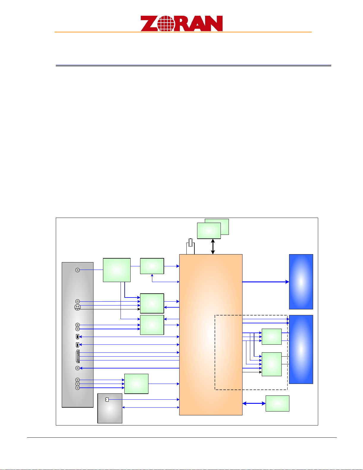
SupraHD-660-680-DTS-GEN-v1.7 -- Preliminary Release
Chapter 1. SupraHD-660/680 Overview
1.1 SupraHD ZR396x0 Family
The ZR396xx family consists of:
• SupraHD-680 IC (ZR39680) - Digital TVs for the ATSC/DVB/OpenCable Market
• SupraHD-660 IC (ZR39660) - Digital TVs for the ATSC Market
• SupraHD-640 IC (ZR39640) - Digital ATSC upgrade for Analog TVs
1.2 SupraHD-660/680 IC Description
The SupraHD-660/680 ICs are members of the SupraHD family of DTV controllers developed by Zoran. These
devices are intended to be used in ATSC-compliant television implementations. They add the functionality
required to support OpenCable implementations. These devices include all of the functionality required to
support the television implementations shown in the following system block diagrams.
S
B
V
C
C
Y
L
R
Rear Chassis
Connections
ATSC/
NTSC
Tuner
Front
Panel
CVBS
Video
A/D
VSB
Analog
Mux
Audio
A/D
TS
16Mx32
CLKIN
Transport
I2C0
CVBS/S-Video In
GPIOx
GPIOx
I2S0
1394 Port0
1394 Port1
HDMI
HI2C
HCEC
IEC958
Unconpressed
Digital HD In*
IRR
UART0
DDR
MIF
ZR39660
LVDS Out
L Audio
R Audio
ACLK
LRCLK
ADATAO0
ADATAO1
ADATAO2
As appropriate for the design
CS0
Stereo
D/A
Virtual
Suround
FLASH
LCD/
PDP
Audio
Amp
Figure 3 SupraHD-660/680 DTV System Diagram - FTA Implementation
3 CONFIDENTIAL INFORMATION-DO NOT COPY 7/12/05
July 12, 2005 6:16 pm
72
Page 73

SupraHD-660-680-DTS-GEN-v1.7 -- Preliminary Release
Figure 4 shows a typical system implementation using the SupraHD-660/680. This system can be designed
and manufactured in a very low-cost manner.
Tuner/
Demod/
NTSC
16Mx32
DDR
Decode
CLKIN
TS
P
C
M
C
I
A
S
B
V
C
C
Y
L
R
TS
TS
CVBS
Analog
MUX
Audio
A/D
Video
A/D
Transport
I2C0
CableCard Out
CableCard In
CableCard Control
CVBS In
GPIOx
GPIOx
I2S0
1394 Port0
1394 Port1
HDMI
HI2C
HCEC
IEC958
Unconpressed
Digital HD In*
MIF
ZR39680
LVDS Out
L Audio
R Audio
ACLK
LRCLK
ADATAO0
ADATAO1
ADATAO2
As appropriate for the design
Stereo
D/A
Virtual
Suround
LCD/
PDP
Audio
Amp
Rear Chassis
Connections
Front
IRR
UART1
CS0
FLASH
Panel
Figure 4 SupraHD-660/680 DTV System Diagram - Open Cable Implementation
7/12/05 CONFIDENTIAL INFORMATION-DO NOT COPY 4
July 12, 2005 6:16 pm
73
Page 74

SupraHD-660-680-DTS-GEN-v1.7 -- Preliminary Release
1.3 I/O Options
Figure 4 shows the four major I/O options available:
• video input and output
• audio input and output
Transport
Processing Unit
1 2
I
I
4
1394
1
0
3
2
2
4
6
11
11
11
13
8
Phy
HDMI
PHY
Video
FE
(TRP)
Xport I/F
Descrambler
1394 Link
Xport Demux
CableCard
I/F
Video Capture
Unit
HDMI
NTSC/PAL
Decoder
BVCI/AVCI BUS (64b)
Display Processor
PVCI BUS (32b )
MIF BUS (64 b)
D
Video Input Options
1. ATSC MPEG2 Transport Stream Input via Serial or Parallel Transport Port
2. DES Encrypted Op en Cable MPEG2 Transport Stream via Serial Transport Port with Parallel Tran sport
to/from the CableCard
1
3. MPEG2 Transport Stream or 5C Encrypted MPEG2 Transport S tream via 1394A Port
4. Uncompressed Digita l Video (YUV or RGB Format) via HDMI Port
5. Uncompressed Digita l Video (YUV or RGB Format) via 24-bit UDI Port
6. NTSC CVBS Analog Video via NTSC/PAL Decoder Port
Audio
Processing Unit
(APU)
L/R
Audio
DACs
(DPC)
Graphics
Video DACs
Video I/F
LVDS Output
(660-680 only)
NTSC
10
4
7
9
2
8
iii
I
i
ii
A
C
5
B
Video Output Options
A. High Definition Analog Output with Macrovision 7.1 Content Protec tion via DAC output
B. Uncompressed Digital Video (YUV or RGB Format) via LVDS Output
A
C. Uncompressed Digital Video (YUV or RGB Format) via Uncompressed Digital Video Port
D. Record Mode via DAC output
Audio Input Options
I. Up to Six (6) channel I2S Input via three (3) I2S Ports
I
II. Two (2) channel PCM A udio Input via the HDMI Port
Audio Output Options
i. Up to Six (6) channel I2S Ou tput via three (3) I2S Ports
i
ii. Two (2) channel Analog Output via DAC Output
iii. IEC958 (S/PDIF) Output
Figure 5 I/O Option Dataflows
5 CONFIDENTIAL INFORMATION-DO NOT COPY 7/12/05
July 12, 2005 6:16 pm
74
Page 75

SupraHD-660-680-DTS-GEN-v1.7 -- Preliminary Release
Chapter 2. Description
This section describes the following:
• Embedded Processing Controller (EPC) on page 7
• Integrated HDMI Link and PHY (SupraHD-660/680 Only) on page 7
• Transport Processing Unit (TRP) on page 8
• Uncompressed Digital Interface (SupraHD-660/680 Only) on page 8
• High-Performance MPEG-2 Video Decoding Engine (SupraHD-660/680 Only) on page 8
• Accelerated 2-D Graphics (SupraHD-660/680 Only) on page 8
• Memory Interface (MIF) on page 9
• Integrated PAL/NTSC Decoder (SupraHD-660/680 Only) on page 11
• 1394A High Speed Interface (Integrated Link and PHY) (SupraHD-660/680 Only) on page 12
• FlexBus Unit on page 11
• General Purpose Input Outputs (GPIOs) on page 13
• Audio Processing Unit (APU) and Audio Output on page 15
• Display Processor (DPC) on page 16
• MPEG-2 Decode Unit (VDEC) on page 19
• Video Scaling and Format Conversion (SupraHD-660/680 Only) on page 21
• Video Processing on page 22
• Device-Unique Chip ID on page 24
• Clock Generation (CLKGEN) on page 24
7/12/05 CONFIDENTIAL INFORMATION-DO NOT COPY 6
July 12, 2005 6:16 pm
75
Page 76

SupraHD-660-680-DTS-GEN-v1.7 -- Preliminary Release
2.1 Embedded Processing Controller (EPC)
The SupraHD-660/680 family uses a MIPS32 4KEc™ processor core, described below.
2.1.1 MIPS32TM Central Processor Unit
The CPU used in the SupraHD-660/680 family is based upon the MIPS32 4KEc core, a member of MIPS®
Technologies MIPS32 4KE™ processor core family. It is a high-performance, low-power, 32-bit MIPS RISC core
designed for custom system-on-silicon applications. The 4KEc core implements the MIPS32 Release 2
Architecture with the MIPS16e™ ASE, and the 32-bit privileged resource architecture. The Memory
Management Unit (MMU) contains 4-entry instruction and data Translation Lookaside Buffers (ITLB/DTLB)
and a 16 dual-entry joint TLB (JTLB) with variable page sizes. The synthesizable 4KEc core includes a
Multiply/Divide Unit (MDU) that implements single-cycle MAC instructions, which enable DSP algorithms to
be performed efficiently. This allows 32-bit x 16-bit MAC instructions to be issued every cycle, while a 32-bit x
32-bit MAC instruction can be issued every 2 cycles.
Instruction and data caches are 8 Kbytes in size. In addition, each cache is 2-way set associative. These caches
are augmented by 10 Kbyte Instruction ROM and 8 Kbyte Data ROM respectively.
2.1.2 MIPS32 4KEc™ Processor Core Data Sheet.
For more detailed information about the MIPS CPU refer to the
website located at
http://www.mips.com
.
Publications
page on the MIPS Technologies
2.2 Integrated HDMI Link and PHY (SupraHD-660/680 Only)
Operational Parameters
• HDMI 1.0 and HDCP 1.1 compliant
• Single HDMI receive port
• Industry-Standard compliance with HDMI 1.0 and HDCP 1.1
• Supports all DTV resolutions (480i/576i/480p/576p/720p/1080i)
• Capable of carrying IEC61937 compressed audio (Dolby Digital, DTS, etc.)
• Integrated High-bandwidth Digital Content Protection (HDCP) cipher
• Direct capture of video, audio, and control information in distinct memory buffers
7 CONFIDENTIAL INFORMATION-DO NOT COPY 7/12/05
July 12, 2005 6:16 pm
76
Page 77

SupraHD-660-680-DTS-GEN-v1.7 -- Preliminary Release
2.3 Transport Processing Unit (TRP)
Operational Parameters
• Total number of simultaneous PID filters: 32
• Maximum Transport Bit Rate: 80 Mbit/sec
• Single Serial Transport Input
• ISO-13818-1 compliant
2.4 Transport Processing Unit (TRP) (SupraHD-660/680 Only)
•ATSC-compliant transport demultiplexer
• Supports Partial Transport and PID filtering
• Support for Single-DES ECB for use with CableCard
• Integrated Open Cable CableCard Interface
• Direct Connect to CableCard (previously known as POD card)
2.5 Uncompressed Digital Interface (SupraHD-660/680 Only)
• 75 MHz digital video input port allowing component video capture up to 1080i
2.6 High-Performance MPEG-2 Video Decoding Engine (SupraHD-660/680 Only)
• Decodes a single High Definition (MP@HL) stream
• Decodes ISO-13818-2 MP@ML, MP@HL
• Decodes all ATSC-compliant formats
• Support for slice-level and frame-level error concealment
2.7 Accelerated 2-D Graphics (SupraHD-660/680 Only)
• Color Space Conversion
• Hardware BLT engine
RGB
— 32-bit-per-pixel
—16-bit αYUV formats
— 1, 2, 4, or 8 bits of index
— Eight Porter-Duff blending operations
α
7/12/05 CONFIDENTIAL INFORMATION-DO NOT COPY 8
July 12, 2005 6:16 pm
77
Page 78

SupraHD-660-680-DTS-GEN-v1.7 -- Preliminary Release
2.8 Memory Interface (MIF)
Operational Parameters
• Maximum DDR Clock Rate: 200 MHz
1
• Maximum DDR Memory: 256 MBytes
• x16, or x32 databus width options
• Unified Memory Architecture that supports all internal processing engines
• High performance arbiter with assignable client priorities
• Up to 1.3 GByte/second peak memory throughput
• 256 MByte memory address range
• SSTL-2 Class 1 electrical interface
The SupraHD-660/680 DDR SDRAM interface provides a high-level interface to memory for each SupraHD660/680 internal memory client.
The interface hides details of the memory organization from clients; the memory organization includes the
complex mapping required to improve memory utilization. The SupraHD-660/680 memory clients
communicate with the memory interface through multiple on-chip memory buses. Each memory request
(descriptor) is transmitted using a descriptor bus, and the data associated with the request is transmitted using
a data bus.
Since the performance of an application depends on the available memory bandwidth or latency for active
memory clients, a priority-based arbitration scheme is implemented in the SupraHD-660/680 memory
interface unit to schedule requests from each memory client in the chip, including memory refresh. The
arbitration scheme can be configured through software drivers to optimize for an application. The winning
request from arbitration circuits is presented to the DDR SDRAM interface circuits for access to the DDR
SDRAM chips.
The SupraHD-660/680 SDRAM interface is compatible with memory chips that conform to the Double Data
Rate (DDR) SDRAM Specification standardized and published by the JEDEC Solid State Technology
Association. The SupraHD-660/680 SDRAM interface supports DDR-400 and DDR-332 memory chips. A
Delay Lock Loop (DLL) circuits is integrated to support the DDR memory read operation.
1. For 200 MHZ DDR operation, MVDD should be 2.6V, +/- 5%.
9 CONFIDENTIAL INFORMATION-DO NOT COPY 7/12/05
July 12, 2005 6:16 pm
78
Page 79

SupraHD-660-680-DTS-GEN-v1.7 -- Preliminary Release
2.8.1 DDR SDRAM Configurations (Chips)
The SupraHD-660/680 memory interface supports one rank of DDR SDRAM chips. Subject to the restriction
described above, Table 1 lists the memory options.
Note: The same memory type must be used for every chip of a configuration.
Table 1. Memory Configuration Options
Total
System
Memory
32MByte
64MByte
128MByte
16-Bit
Interface
16M x 16
32M x 16
64M x 16
32-Bit
Interface
8M x 16 (2) 128 Mbit
16M x 16 (2)
32M x 16 (2)
64M x 16 (2)
DDR Size
256 Mbit
512 Mbit
1 Gbit
2.8.2 Hardware Connection
The SupraHD-660/680 supports a point-to-point connection to the DDR devices utilizing series termination.
Refer to the Zoran reference board design layout documentation for specific information about the interface
parameters (trace length, capacitance, etc.) and termination resistors. This information can be obtained from
your Zoran representative.
7/12/05 CONFIDENTIAL INFORMATION-DO NOT COPY 10
July 12, 2005 6:16 pm
79
Page 80
SupraHD-660-680-DTS-GEN-v1.7 -- Preliminary Release
2.9 Integrated PAL/NTSC Decoder (SupraHD-660/680 Only)
• 3 D adaptive comb filter
— Eliminates dot crawl from vertical or horizontal transitions
— Eliminates dot craw from single pixel lines
— Eliminates false color from high frequency horizontal luma
— Performs ideal YC separation for still image
— No loss in horizontal or vertical chroma detail
— No loss in horizontal or vertical luma detail
— Performs well both on real video images and on test patterns
• Adaptive horizontal PLL
— Automatically adjusts loop bandwidth for signal conditions
— Automatically detects VCR source and enters optimum tracking mode; most decoders require a “VCR
mode” bit to be set to optimally handle VCR signals
— Automatically detects VCR special effects mode and compensates
— Comb filter automatically disabled when VCR source is detected
• Robust sync and DC setup acquisition
— DC setup and sync recovery is very robust even in the presence of noise, ghosting, and unlock
condition
— Automatic switch over to “fine” mode operation once rough lock is acquired
• Chroma edge enhancement
— Improves the horizontal transition of the chroma edge
• VBI decoder
— Performs VBI data capture and data slicing embedded in the video lines
Table 2 VBI Data Types (SupraHD-660/680 Only)
VBI Data Type Va lid VBI Data Li ne
US Closed Caption Line 21, 284 for NTSC 2-byte
EURO Closed Caption
Teletext 625A Programmable 37-byte
Teletext 625B / WST625 Programmable 42-byte
Teletext 625C Programmable 33-byte
Teletext 625D Programmable 34-byte
Teletext 525B / WST525 Programmable 34-byte
Teletext 525C / NABTS Programmable 33-byte
Teletext 525D Programmable 34-byte
WSS625
GemStar Closed Caption Programmable 4-byte
Line 18, 281 for PAL M
Line 22, 335 for PAL
B,D,G,H,I,N,CN
Line 17, 280 for PAL M
Line 23, 336 for PAL
B,D,G,H,I,N,CN
(Excluding Start Code
2-byte
14-bit (~2-byte)
Data Length
or Frame Code)
WSSJ Line 20, 283 for NTSC 20-bit (~3-byte)
VPS
11 CONFIDENTIAL INFORMATION-DO NOT COPY 7/12/05
Line 16 in Germany,
Austria and Switzerland
July 12, 2005 6:16 pm
13-byte
80
Page 81

SupraHD-660-680-DTS-GEN-v1.7 -- Preliminary Release
2.10 1394A High Speed Interface (Integrated Link and PHY) (SupraHD-660/680 Only)
• Provides two (2) P1394a fully-compliant cable ports at 100/200/400 megabits per second (Mbits/s)
• Embedded support for 5C/DTCP content protection:
— Four M6 baseline ciphers (one per HSDI port)
— Random number generator in software
— SHA-1 secure hash algorithm in software
— Authentication key cipher in software
• Compliant with IEEE 1394-1995 and IEEE 1394a–2000 standards
• MPEG2 time stamp-based release, as described in IEC 61883-1,2,3,4
• Complies with ANSI/SCTE 26 as a sink
• Complies with EIA-799 as a sink
• Supports CEA-931-A pass-through control commands
• Interoperable with other physical layers (PHYs) using 3.3-V and 5.0-V supplies
• Separate cable bias (TPBIAS) for each port
81
Page 82

SupraHD-660-680-DTS-GEN-v1.7 -- Preliminary Release
2.11 FlexBus Unit
2.11.1 System Interface
The Flexbus of the SupraHD-660/680 contains several common interfaces required for system design and
operation. These include:
• CableCard support (660/680 only)
2
C x 3
•I
•UART x 2
•IRR
•GPIO
•GuestBus
— 6 Chip Selects
— NAND and NOR FLASH support, including Boot-From-NAND for lowest system cost
— Secure boot
— 8-bit and/or 16-bit device-width support
— Up to 64 MB of address space
2.11.2 I2C Controllers
Operational Parameters
• Maximum Baud Rate: 400 Kb/s
• Two physical ports
• Master or Slave mode
2
The I
C-compatible interfaces are designed to be the control buses within the system that control the general
purpose interfaces such as the Demodulator/Tuner, and a command interface with the Host system. The
SupraHD-660/680 I
2
C function is I2C-compliant and compatible as long as it meets the following
requirements:
2
C-compatible bus supports any IC fabrication process: NMOS, CMOS, bipolar. Two wires, serial data
The I
and serial clock, carry information between the devices connected to the bus.
2
Number of I
C interfaces supported by each model is listed above in Section 2.4.1, “System Interface.”
13 CONFIDENTIAL INFORMATION-DO NOT COPY 7/12/05
July 12, 2005 6:16 pm
82
Page 83

SupraHD-660-680-DTS-GEN-v1.7 -- Preliminary Release
2.11.3 Universal Asynchronous Receiver Transmitter (UART)
Operational Parameters
• Maximum Baud Rate: TBD
•Two (2) UARTs
Overview
The SupraHD-660/680 UARTs are functionally identical to the 16450 on powerup, and UART A can be placed
in an alternate mode (FIFO mode) to relieve the CPU of excessive software overhead.
In this mode, internal FIFOs are activated allowing 16 bytes (plus 3 bits of error data per byte in the RCVR
FIFO) to be stored in both receive and transmit modes. All logic is on-chip to minimize system overhead and
maximize system efficiency. Two individual interrupts allow signalling of data transfers, one for transmit and
one for receive.
The UART performs serial-to-parallel conversion on data characters received from a peripheral device or a
MODEM, and parallel-to-serial conversion on data characters received from the CPU. The CPU can read the
complete status of the UART at any time during the functional operation. The status information reported
includes the type and condition of the transfer operations being performed by the UART, as well as any error
conditions (parity, overrun, framing, or break interrupt).
The UART includes a programmable baud rate generator that is capable of dividing the timing reference clock
input by divisors of from 1 to (2
Provisions are also included to use this 16x clock to drive the receiver logic.
UART A has complete MODEM-control capability, and a processor-interrupt system. Interrupts can be
programmed to satisfy user requirements, minimizing the computing needed to handle the communications
link.
16
-1), and producing a 16x clock for driving the internal transmitter logic.
7/12/05 CONFIDENTIAL INFORMATION-DO NOT COPY 14
July 12, 2005 6:16 pm
83
Page 84

SupraHD-660-680-DTS-GEN-v1.7 -- Preliminary Release
2.12 General Purpose Input Outputs (GPIOs)
The GPIOs are bidirectional signals used for various applications within the system. Some of the ports, if not
used for their primary function, can be converted to GPIOs and used for different functions. The Four (4)
GPIOs in the SupraHD-660/680 are dedicated to GPIO functionality.
After power-up or reset, the multiplexed GPIO pins wake up as defined by the primary function of each
individual pin. Software can select the functionality of the GPIO pins — either GPIO or a secondary function
— according to the system configuration. The selection is done for each GPIO individually.
• If GPIO functionality is selected, the secondary functionality returns a constant value to the internal
blocks, and outputs are not used.
— When configured as an output, the GPIO pin continuously drives with a high or low level, according
to the bit value of the corresponding register.
— When configured as an input, the GPIO pin value is continuously sampled and stored in the
corresponding register bit. When a specific bit in the direction register changes, the direction change is
immediate.
• If the secondary functionality is active, the GPIO input register remains active (not tied off), and the GPIO
outputs are not used.
Each GPIO pin can also serve as an external interrupt input pin for the SupraHD-660/680. On each GPIO input
there is a programmable edge detection for an interrupt on either the positive or negative edge (or both edges).
Software should disable the GPIO interrupts when updating the GPIO functionality, direction, or edge
selection to avoid false interrupts.
2.12.1 GuestBus
The SupraHD-660/680 has a generic general purpose parallel address/data bus named GuestBus. The
interface is designed for asynchronous, microcontroller bus-like devices. It allows the SupraHD-660/680 to
perform data transfer between the internal PVCI bus and externally connected ‘guest’ slave devices.
The GuestBus supports single-CPU write and read access. It has a generic timing and signaling interface which
makes it compatible with a wide variety of multimedia and storage devices including:
• NAND or NOR Flash memory devices (no execution); typically boot only.
• PCMCIA 16-bit PC Cards, such as Compact Flash cards.
15 CONFIDENTIAL INFORMATION-DO NOT COPY 7/12/05
July 12, 2005 6:16 pm
84
Page 85

SupraHD-660-680-DTS-GEN-v1.7 -- Preliminary Release
2.12.2 Flash Connection Examples
Figure 5, Figure 6 and Figure 7 provide examples of Flash connections, using the SupraHD-660/680.
SupraHD Processor
GCS0#0
GuestBus Interface
SupraHD Processor
GuestBus Interface
GDAT[7:0]
GADR[1]
GADR[0]
GOE#
GWE#
GPIO
GPIO
GDAT[7:0]
GADR[23:0]
GCS0#
GOE#
GWE#
GPIO
GPIO
NAND Flash
IO[7:0]
CLE
ALE
CE#
RE#
WE#
READY
WP
Figure 6 Unbuffered NAND Flash
NOR Flash
IO[7:0]
ADDR[23:0]
CE#
RE#
WE#
READY
WP
Figure 7 Unbuffered 8-bit NOR Flash
7/12/05 CONFIDENTIAL INFORMATION-DO NOT COPY 16
July 12, 2005 6:16 pm
85
Page 86
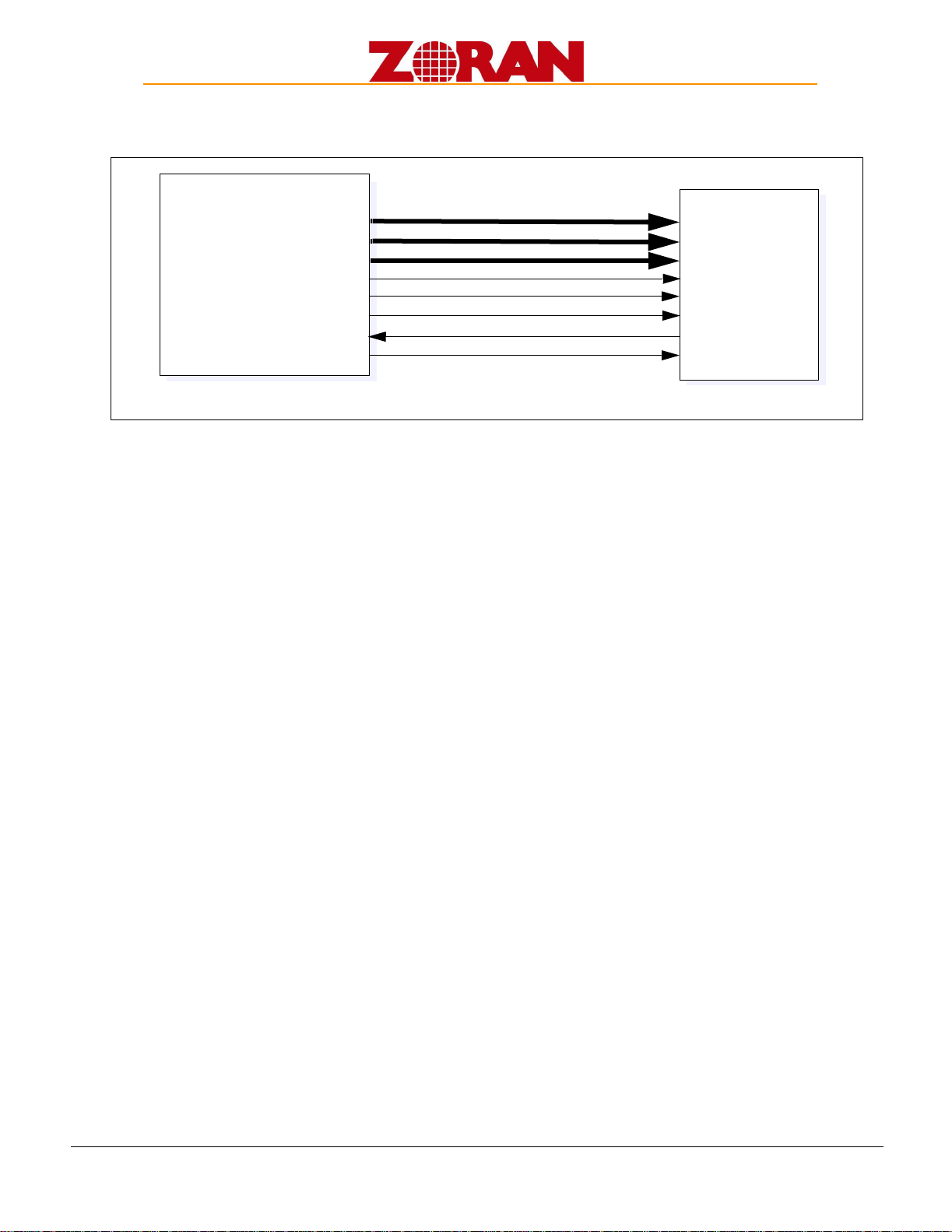
SupraHD-660-680-DTS-GEN-v1.7 -- Preliminary Release
SupraHD Processor
GADR[23:16](GDAT[15:8])
GuestBus Interface
GDAT[7:0]
GADR[15:0]
GCS0#
BGOE#
BGWE#
GPIO
GPIO
Figure 8 Unbuffered 16-bit NOR Flash
NOR Flash
IO[7:0]
IO[15:0]
ADDR[15:0]
CE#
RE#
WE#
READY
WP
2.13 Audio Processing Unit (APU) and Audio Output
The SupraHD-660/680 has a single stereo audio output, containing left and right channels, using a differential
pair output, which requires op amps in the system design to support and drive the audio output. Please refer
to the SupraHD-660/680 reference design for more information about the connection of the SupraHD-660/680
to a system amplifier or speakers.
The SupraHD-660/680 supports the following:
• AC3 audio decode
— 5.1 channel or 2 channel downmix
— 24-bit precision
• Integrated stereo audio DACs
• Audio Playback from unified memory
• Audio select, mix, cross-fade, and attenuate all audio sources
2
•I
S inputs (3 ea.) support 6 audio input channels
2
S outputs (3 ea.) for connection to optional external audio DACs
•I
• Supports multiple serial data formats
• Supports sample rates up to 96 KHz
• IEC-958 output of Encoded or PCM audio data
The SupraHD-660/680 has a single stereo audio output, containing left and right channels, using a
deferential pair output, which requires op amps in the system design to support and drive the audio
output. Please refer to the SupraHD-660/680 reference design for more information about the connection
of the SupraHD-660/680 to a system amplifier or speakers.
2.13.1 L/R Analog Stereo DAC Output
TBD
2.13.2 Synchronization
The SupraHD-660/680 provides audio/video synchronization through system-level software control. Video is
slaved to the audio subsystem.
17 CONFIDENTIAL INFORMATION-DO NOT COPY 7/12/05
July 12, 2005 6:16 pm
86
Page 87

SupraHD-660-680-DTS-GEN-v1.7 -- Preliminary Release
2.14 Display Processor (DPC)
This section describes DPC features of the SupraHD-660/680.
2.14.1 Features of the SupraHD-660/680
• Dual Display Output (Primary DPC, Secondary DPC)
• Main output display formats include 1920x1080I, 1280x720P, (EIA-770.3A), 720x480P, and 720x480I (EIA-
770.2A)
• Second Video Outputs NTSC/PAL/SECAM Video only, no OSD
• Analog output in RGB or YCrCb with optional 3-level sync, and/or digital HSync and VSync
— 10-bit video processing
— Four 10-bit DACs (RGB/YPbPr/Y/C/CVBS)
— Oversampling to 166 MHz. Allows single low-cost reconstruction filter for all output resolutions
©
— Video output signals may be copy-protected using CGMS Layer 1/2 and DirecTV
—Macrovision© 7.1 encoding, supported on analog output in YCbCr mode
Figure 9 shows the basic video output paths in the SupraHD-660/680. The second video path is fully
independent of the Main path in terms of timing, and supports only NTSC/PAL output resolution.
CGMS
Primary DPC
Memory
All Format
Main
Video
Scaler
All Format
Display
Secondary DPC
Display
Memory
nd
480i
480i CVBS (Y/C)
Figure 9 Video Output Pipelines
2
Video
Scaler
NTSC/
PAL
Encoder
Note: This figure is intended to show the relationship between the main and secondary video
paths NOT the entire video output structure.
• Graphics resolution up to full screen output at 32 bits/pixel or 8 bits/pixel
• Digital Video Output — 24 bbp Flat Panel Support (multiplexed with uncompressed digital input)
• Dual Channel 24 -bit LVDS drivers for flat panel displays
• Support for non-standard resolutions such as 1280x768p, 852x480p, 1024x768p, 1366x768p
• EIA-608 and EIA-708 Closed Caption support
The MPEG-2 VDEC supports:
• decode of a single High Definition (MP@HL) stream
• decodes of ISO-13818-2 MP@ML, MP@HL
• decode of all ATSC-compliant formats
• Slice-level and Frame-level error concealment
7/12/05 CONFIDENTIAL INFORMATION-DO NOT COPY 18
July 12, 2005 6:16 pm
87
Page 88

SupraHD-660-680-DTS-GEN-v1.7 -- Preliminary Release
2.14.2 YPbPr DC Output Levels and Amplitudes
This section provides the following DC output level and amplitude information for the YPbPr signal lines:
• SupraHD-660/680 YPbPr signals are output via 10-bit DACs.
• An external RSET resistor determines the range of YPbPr signal values. This RSET resistor provides a full
dynamic range under an external load of 37.5 ohms on the YPbPr lines.
• YPbPr digital levels are:
— The Y digital levels run from 16 to 235
— The PbPr digital levels run from 16 to 240
• YPbPr (approximate) minimum and maximum voltage amplitudes are:
— Y Sync LOW level is 50 mV.
— Y Blank Level is 350 mV (can be adjusted to 286 mV if necessary).
— Y Sync HIGH level (for tri-level Sync) is 650 mV.
— Y maximum level is 1050 mV.
— PbPr minimum level is 50 mV.
— PbPr maximum level is 750 mV.
19 CONFIDENTIAL INFORMATION-DO NOT COPY 7/12/05
July 12, 2005 6:16 pm
88
Page 89
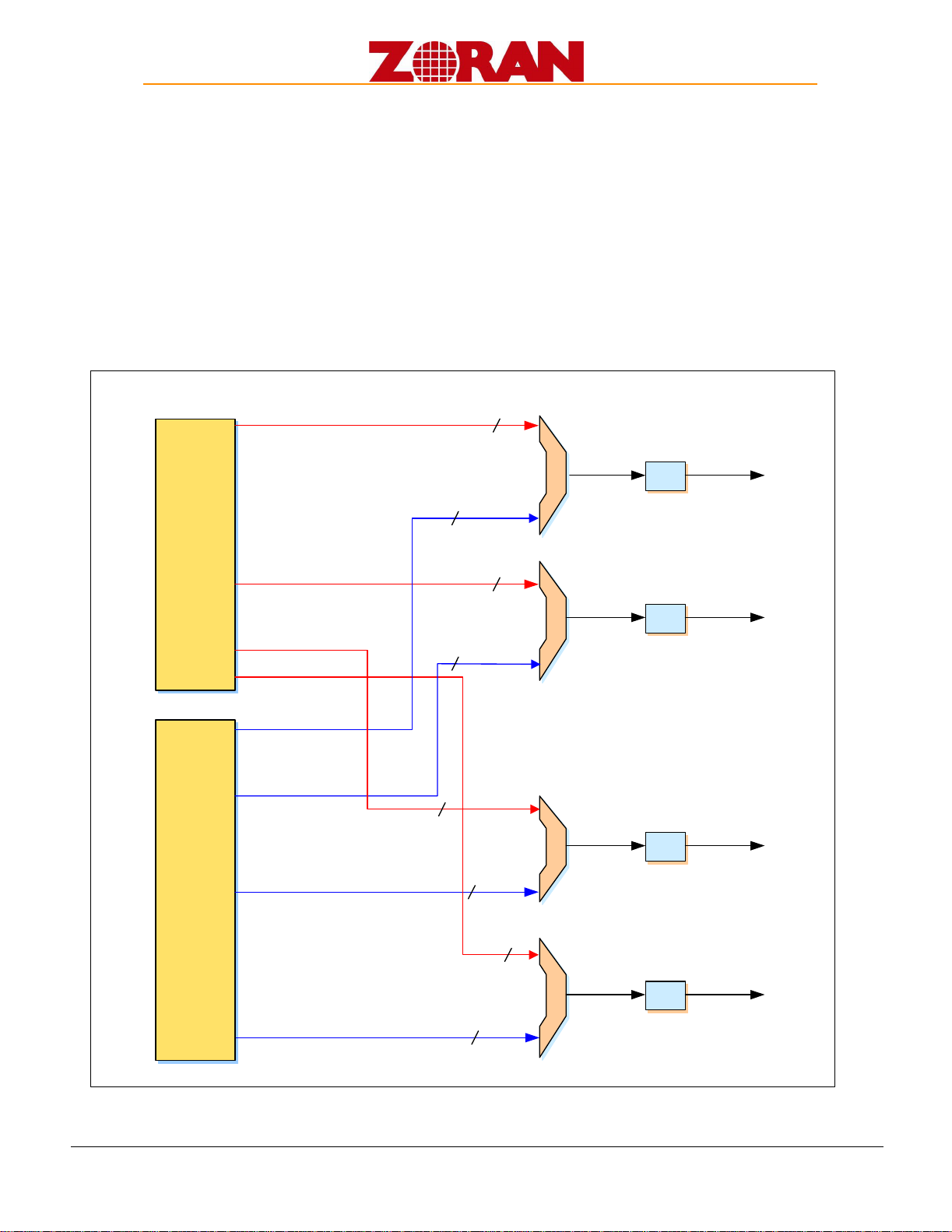
SupraHD-660-680-DTS-GEN-v1.7 -- Preliminary Release
2.14.3 Analog Video Display Outputs
Video outputs from the SupraHD-660/680
•HD Analog Video
• CVBS Analog Video
•Y/C Analog Video
• four DACs are shared between the two analog video outputs
• video output from either the Primary DPC or the Secondary DPC
Figure 8 shows the four on-board 10-bit DACs that are used to support the analog output modes of the
SupraHD-660/680. When the main video output requires component output, the secondary video output is
limited to composite only (S-Video is not available).
6:1 Muxes
R/G/B/Y/Pb/Pr
(4)
3
Main
Video
Out
nd
2
Video
Out
(Aux)
Main: One of six si gnals on each of the three lines
R/G/B/Y/Pb/Pr
R/G/B/Y/Pb/Pr
R/G/B/Y/Pb/Pr
Y/C/CVBS
Y/C/CVBS
Y/C/CVBS
Aux: One of three signals on each of the three lines
DAC
Y/C/CVBS
3
3
DAC
Y/C/CVBS
3
R/G/B/Y/Pb/Pr
3
DAC
3
R/G/B/Y/Pb/ Pr
3
DAC
Y/C/CVBS
3
Figure 10 Video DACs for Analog Output Modes
7/12/05 CONFIDENTIAL INFORMATION-DO NOT COPY 20
July 12, 2005 6:16 pm
89
Page 90

SupraHD-660-680-DTS-GEN-v1.7 -- Preliminary Release
2.15 MPEG-2 Decode Unit (VDEC)
The MPEG-2 VDEC supports:
• decode of a single HD (MP@HL) stream
• decodes of ISO-13818-2 MP@ML, MP@HL
• decode of all ATSC-compliant formats
• Slice-level and Frame-level error concealment
The decoder engine can decode MPEG-compressed bitstreams as defined in the following specifications:
• ISO/IEC 13818-2, “Information Technology - Generic Coding of Moving Pictures and Associated Audio
Information: Video,” (Up to MP@HL)
•A/53, “ATSC Digital Television Standard,” (Table 3)
• DTVMDB04, “DIRECTV MPEG-2 Video Bitstream Specification for the IRD”
In the SupraHD-660/680, this engine is designed to decode a single HD or SD bitstream.
2.16 Video Scaling and Format Conversion (SupraHD-660/680 Only)
• High-quality up-conversion and down-conversion of source video to selected display format
• High-quality scan conversions from ATSC, and NTSC/PAL source formats to many output display
formats
• “Letterbox” and “Pan & Scan” options to convert 16:9 material to 4:3 aspect ratio
• Waterglass stretch of 4:3 material to 16:9 aspect ratio
21 CONFIDENTIAL INFORMATION-DO NOT COPY 7/12/05
July 12, 2005 6:16 pm
90
Page 91
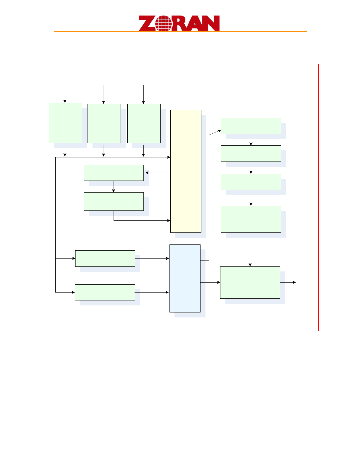
SupraHD-660-680-DTS-GEN-v1.7 -- Preliminary Release
2.17 Video Processing
Figure 11 illustrates the SupraHD-660/680 Video Processing block diagram and dataflow.
SD/HD MPEG
Decoder
Composite
Video
Decoder
3D-Comb
2D/3D Noise Reduction
Motion Adaptive
Deinterlacer with Diagonal
Interpolation
Black Bar Detection
Signal Staistics Collection
External
Video
Capture
Ext
Memory
CPU
Up/Down Panorama Scaler
Edge Enhancement
Selective Color Correction
3x3 Matrix
(Color Space Conversion,
Color Temperature,
Adjustments)
Triple Look-up Table
(Gamma Correction,
Adaptive Contrast
Enhancement)
Figure 11 SupraHD-660/680 Video Processing Data Flow
2.17.1 2D/3D Noise Reduction
The Video Processing block provides adaptive temporal/spatial noise reduction, removing Gaussian, Salt and
Pepper, Striking, and Color noises. It preserves edges and prevents ghost artifacts, and adjusts adaptively to
the type and amount of the noise.
7/12/05 CONFIDENTIAL INFORMATION-DO NOT COPY 22
July 12, 2005 6:16 pm
91
Page 92

SupraHD-660-680-DTS-GEN-v1.7 -- Preliminary Release
2.17.2 Color Space Conversion
Color Space Conversion supports all required color space conversions including but not limited to:
• RGB to YCbCr, and vice versa
• ITU-R BT.601 to ITU-R.BT1361, and vice versa
2.17.3 Video Adjustments
The following factory/user video adjustments are supported:
•brightness
• contrast
•saturation
•tint (hue)
•color temperature
• black and white balance
2.17.4 Gamma Correction
Fully-programmable 10-bit gamma correction is supported.
2.17.5 Adaptive Contrast Enhancement
Adaptive Contrast Enhancement adaptively adjusts the luminance transfer characteristic. This dramatically
enhances the visual contrast without clipping black or white.
2.17.6 Motion Adaptive Deinterlacer with Diagonal Interpolation
The Motion Adaptive Deinterlacer supports the following:
• motion adaptive pixel-based algorithm selections with smooth transition
• low angle diagonal interpolation
• fast automatic movie-mode detection, with reverse 3:2 and 2:2 pull-down
2.17.7 Picture Statistics Collection and Black Bar Detection
The Video Processing block collects histogram data distribution information, and detects black bar presence
and positioning. The data is used for Adaptive Contrast Enhancement and selection of an appropriate Scaling
factor.
2.17.8 Edge Enhancement
Edge enhancement supports the following:
• flexible sharpening/softening adjustment
• edge-acceleration optimized for minimum overshoot/undershoot and noise amplification
2.17.9 Selective Color Correction
Selective Color Correction allows adjustment of local color without affecting other colors. SCC supports four
independent fully-programmable color areas.
23 CONFIDENTIAL INFORMATION-DO NOT COPY 7/12/05
July 12, 2005 6:16 pm
92
Page 93

SupraHD-660-680-DTS-GEN-v1.7 -- Preliminary Release
2.18 Device-Unique Chip ID
• 128-bit device unique secret key
• On-chip tamper-proof AES security services engine enables platform-unique secure storage of
— Digital certificates for OpenCable DFAST
— HDMI keys
—5C keys
— Application code
—Other secrets.
Clock Generation (CLKGEN)
The clock generation unit within the SupraHD-660/680 includes an integrated digital VCXO and PLL that
generate the various clocks used in the SupraHD-660/680. Nine internal clocks are generated by the CLKGEN
circuitry, used to drive the various subsystems within the SupraHD-660/680.
7/12/05 CONFIDENTIAL INFORMATION-DO NOT COPY 24
July 12, 2005 6:16 pm
93
Page 94

SupraHD-660-680-DTS-GEN-v1.7 -- Preliminary Release
Chapter 3. Functional Operation
3.1 Boot Process
The boot process of the SupraHD-660/680 is a multiple-stage procedure that utilizes internal IROM code and
external configuration inputs to set-up the CPU and determine the external boot device. The external boot
device may be physically located on the GuestBus, I
3.1.1 First Stage Boot
In the first stage of the boot process, the SupraHD-660/680 CPU begins by executing encrypted code from its
internal IROM. This IROM is programmed by the factory and contains enough code to initialize the CPU and
identify the second stage boot options.
3.1.2 Second Stage Boot
In the second stage of the boot process, the SupraHD-660/680 examines electrical levels on the
to determine where the OS/Boot image is stored. Table 2 defines the options available for the second stage
boot.
2
C bus, or UART interface.
GPIO[3-0]
balls
Table 3. SupraHD-660/680 Boot Option
SupraHD-660/680 Boot Option
Reserved 0000
16-Bit NAND — Large Page
16-Bit NOR 1010
16-Bit NAND — Small Page 1011
SPI 1100
8-Bit NAND — Large Page 1101
8-Bit NOR 1110
8-Bit NAND — Small Page 1111
1. Large Page NAND Flash is typically larger than 64 Mbytes.
1
GPIO3 GPIO2 GPIO1 GPIO0
1001
Once the boot device is identified, the CPU will then execute the code in the first 8 KBytes of the boot device.
This 8 KBytes of code is used to initialize the remainder of the SupraHD-660/680 IC. This code is encrypted
and is supplied by Zoran to the system developer.
Note: Please contact your Zoran sales representative for more information about receiving and/or
customizing the 8 KByte boot code.
3.1.3 Third Stage Boot
The third stage of the boot process loads the O/S and user-defined Application(s).
25 CONFIDENTIAL INFORMATION-DO NOT COPY 7/12/05
July 12, 2005 6:16 pm
94
Page 95

SupraHD-660-680-DTS-GEN-v1.7 -- Preliminary Release
3.2 Power-Up Sequencing
Figure 10 shows the recommended timing relationships for the power supplies of the SupraHD family of DTV
single chip ICs. This timing should be used to insure proper operation of systems based upon the SupraHD660/680.
Vnominal
IOVDD
≥
0
MVDD
VREF
CVDD
RESET_N
GPIO[3:0]
CLK_IN (
24.576 MHz
Tcl k
(20 cycles)
)
Figure 12 SupraHD-660/680 Power Sequencing
≥
0
Please note the following voltage references:
= I/O Supply = 3.3 V ± 5%
IOVDD
•
•
MVDD
= Memory Supply = 2.5 V ± 5%
CVDD
= Core Supply = 1.8V ± 5%
•
= Memory Voltage Reference = 1.25 V ± 5%. Programming Model
•
VREF
Power-Off Reset
Treset
100mS(min)
Boot Configuration
10mS
GPIO
Normal Operation
Power-On Reset
100 mS (min)
Boot
GPIO
7/12/05 CONFIDENTIAL INFORMATION-DO NOT COPY 26
July 12, 2005 6:16 pm
95
Page 96

AML3278 A/V Processor User Guide Version 0.71
9.2
13-AML327-80B IC AML3278 U4
AML 3278 A/V Processor
User’s Guide
Amlogic, Inc.
3970 Freedom Circle
Santa Clara, CA 95054
U.S.A.
www.amlogic.com
Amlogic reserves the right to change any information described herein at any time without notice.
Amlogic assumes no responsibility or liability from use of such information.
12/21/2005 1/40 Amlogic Proprietary
96
Page 97

AML3278 A/V Processor User Guide Version 0.71
1 Introduction
The AML3278 A/V processor is a completely integrated system targeting all types of Audio/Video decoder
applications that provide connectivity to hard disk, digital camera, MP3 players and other external digital
consumer devices. The target market for AML3278 A/V processor is feature rich DVD players, audio
receivers, DVD/receiver combo players, digital media players, integrated TV media players, portable DVD
players, and portable media players.
The AML3278 combines full function of MPEG-1, MPEG-2 and MPEG-4 decoding, numerous dedicated
and general-purpose peripherals, and a high speed 32-bit host CPU in a single device. The AML3278
has three built-in AMRISC
servo-loop digital signal processing. The AML3278 also provides a high speed interface to external USB
1.1/2.0 chip for connectivity to popular USB devices like hard disk, Flash memory, and digital camera and
MP3 players.
The embedded 32-bits host CPU handles system initialization, DVD navigation, and other system
applications. The AML3278 A/V processor provides a glueless interface to all external components:
ATAPI loaders, USB interface chip, HDMI transmitter chip, audio DACs and memory. Numerous generalpurpose I/O pins can be used to control the front panel display and other miscellaneous tasks. Together,
the embedded host CPU and special glueless interfaces reduce the total system cost for all A/V
applications from any media.
The AML3278 A/V processor features a sophisticated video sub-system that performs video
enhancement and scaling functions. It supports DVD up-scaling capabilities to 720p and 1080i
resolutions for the TV system. In addition, a digital TV interface is created for connecting to external
HDMI or DVI transmitter for 100% digital solution between the DVD and TV systems. The digital TV
interface is designed to work with a companion HDMI transmitter (AML3505) to drive the serial HDMI/DVI
signals.
The video sub-system also integrates an NTSC/PAL TV encoder for traditional analog video outputs like
S-Video, composite, YUV component, RGB and multiple VGA modes. The video encoder also supports
high-quality de-interlaced progressive scan (480p/576p) with full Macrovision support. Contrast
enhancement, hue adjustment, video scaling, video interpolation, pan-scan, letter-box, and zoom are also
supported. In addition, four built in video DACs complement the video encoder further reducing system
cost.
The integrated Audio AMRISC
processing. The micro-coded engine provides support for all existing audio formats and it also has
enough flexibility to accommodate new audio standards. Popular audio formats like MPEG, LPCM, Dolby
AC-3 5.1, HDCD, MP-3 and WMA are supported. In addition, SPDIF (IEC958) input and outputs are
supported. AML3278 also supports the MLP loss-less compression and PCM format for DVD-Audio with
sample rate up to 192 KHz for two channels and 96 KHz for multi-channels.
Since AML3728 supports DVD-Audio, the Audio AMRISC processor also supports MLP and high sample
rate PCM audio formats.
The USB interface provides the necessary high speed interconnections to an external USB chip. The
external USB chip can support up to 2 high-speed USB ports. The AML3278 firmware includes the basic
USB device driver, USB protocol stacks to support bulk and INTR transfer, Hub, Mass-Storage (MS) class,
Picture Transfer Protocol (PTP) and PictBridge protocol. The USB firmware also supports multiple file
systems and includes flexible file transfer functions between USB devices.
TM
RISC processors with special instructions to accommodate audio, video and
TM
RISC processor performs advanced digital audio decoding and post-
12/21/2005 5/40 Amlogic Proprietary
97
Page 98

AML3278 A/V Processor User Guide Version 0.71
The AML3278 also integrates a flexible disc loader front-end with complete servo control, signal recovery,
descrambling, and error detection and correction. The analog front-end features high resolution ADC and
DAC for servo control. A front-end optimized AMRISC
TM
RISC processor performs adaptive servo
tracking algorithms and provides unique intelligence to work with disk media errors. The loader front-end
is designed to work with a companion RF front-end chip (AML 3501) for interfacing to an OPU.
The adaptive AMPOWER-I algorithm is integrated into both the chip design and the firmware to reduce
power consumption for portable applications. AMPOWER-I also provides higher performance within
smaller, thermally constrained environments.
12/21/2005 6/40 Amlogic Proprietary
98
Page 99

AML3278 A/V Processor User Guide Version 0.71
2 Features
The AML3278 chip is very flexible and most of the capabilities are under firmware control. The following
list of features may or may not be included in the firmware library or binary, depending on the actual
application and platform.
High Integration
o Embedded 32-bits RISC processor for system control
o Integrated disc servo front-end with complete servo control, signal recovery,
descrambling, and error detection and correction
o Glueless interface to dual ports USB controller
o Complete MPEG 1/2/4 decoding backend and video post processing logic
o Complete audio decoding backend
o Integrated TV encoder and Video DACs
MPEG 1/2 Decoding
o MPEG video engine controlled by dedicated Video AMRISC
o MPEG-2 ML/MP conforming to ISO-13818
o MPEG-1 ML/MP conforming to ISO-11172
o On-chip CSS descrambler
o Compliant with DVD Specification 1.0 for read-only Disc decoding
o DVD Sub-picture and highlight decoding and display
o Advanced error detection, concealment, and recovery scheme
o Backward compatible VCD (1.0 to 3.0) decoding
o Super VCD decoding
MPEG 4 Decoding
o MPEG-4 and DivX 3.x/4.x/5.x compliant
o GMC and Q-Pel compatible
o Digital Right Management (DRM) engine for content management
o Multiple language DivX sub-title support
Video Processing
o 3:2 pull-down for 24 fps displaying at 30 fps
o 2:2 pull-down for 24 fps displaying at 25 fps
o Automatic frame rate adoption when playing non-DVD/VCD contents (like .mpg and .avi
files)
o Adaptive pixel-based de-interlacing algorithm
o Variable steps video zooming (up to 8x)
o Letterboxi and pan/scan
o Special trick modes:
Pause, single-step
slow motion
reverse playback
Multiple steps fast forward/backward
o Built-in NTSC to PAL scaling or vice-versa
o On-Screen-Display (OSD) capable of supporting up to 256 fixed colors or 16
programmable colors
o OSD alpha-blending over video display
TV Encoder
o Interlaced NTSC output 720x480 at 30 fps, with Macrovision 7.1L1 anti-taping
o Interlaced PAL output 720x576 at 25 fps, with Macrovision 7.1L1 anti-taping
12/21/2005 7/40 Amlogic Proprietary
TM
processor
99
Page 100

AML3278 A/V Processor User Guide Version 0.71
o Progressive NTSC output 480p at 60 fps, with Macrovision 1.03 anti-taping
o Progressive PAL output 576p at 50 fps, with Macrovision 1.03 anti-taping
o High definition output of 720p and 1080i at 50/60 fps
o VGA output for computer monitors and LCD panels. VGA (640x480), SVGA (800x600),
XVGA (1024x768) and SXVGA (1280x1024) are supported
o Interlaced S-Video, component, composite and SCART output
o Simultaneous output of progressive and interlaced video
o Closed caption modulation in the vertical blanking intervals
o WSS/CMGS insertion
o CCIR656 and CCIR 601 YCbCr output digital LCD panel connections
o Full resolution (up to 1920x1080i) digital video output for HDMI/DVI connection
o Programmable tint, brightness and other TV enhancements
Graphics
o Graphics engine supports JPEG and BMP image decoding
o Graphics can be scaled independently of the video output
o Unified MPEG video and graphics memory architecture for maximum flexibility and
system cost savings
Audio Decoding
o Built-in Audio AMRISC
TM
processor with extensions specifically designed for audio
processing
o On-the-fly switching of audio streams during playback
o Full MPEG audio layers I, II and III
o Compliant with Dolby AC-3 5.1 channel decoding
o DVD-Audio with full CPPM processing
o HDCD support
o MP3 music CD/DVD support
o WMA music CD/DVD support
Audio Post Processing and Output
o Supports 8 channels linear PCM output. I
2
S or EIAJ DAC-compatible
o IEC958 (S/PDIF) digital output
o DTS audio pass-through
o AC-3 two channels down-mixing
o Virtual surround sound to create 3-D spatial sound field from two audio channels
o Prologic II to convert stereo audio source to multi-channel audio output
o Full speaker configurations and bass management with adjustable crossover settings
o Muting, volume control, etc.
o Karaoke functions like integrated echo control and key control.
Audio Input
o IEC958 (S/PDIF) digital input with frame decoding to accommodate A/V receiver
applications
o PWM signals for tracking clock difference for external audio inputs
o Two channels analog audio input
Front-end Loader Interface and Control
o Direct interface to AML3501 Front-End RF device for DVD/CD loader support
o DSP servo control with adaptive servo tracking algorithm
o Support up to 6x DVD speed and 24x CD speed
o Supported medias:
DVD-Video (from DVD-ROM. DVD±R and DVD±R/W)
VCD and DVCD (from CD-ROM, CD±R and CD±RW)
12/21/2005 8/40 Amlogic Proprietary
100
 Loading...