

Page 1

TCL
SERVICE MANUAL
48D2700/MT56B-AP
1. Caution…………………………………………………………………………
2. specification……………………………………………………………………
3. Alignment Procedure…………………………………………………………
4.Block diagram…………………………………………………………………
5.Scheme Diagram ……………………………………………………………
6. Troubleshooting………………………………………………………………
([SORGHGUDZLQJ
This m anual i s t he l atest at t he t ime of pr inting, and doe s not
include the modification which may be made after the printing, by
the constant improvement of product
Page 2
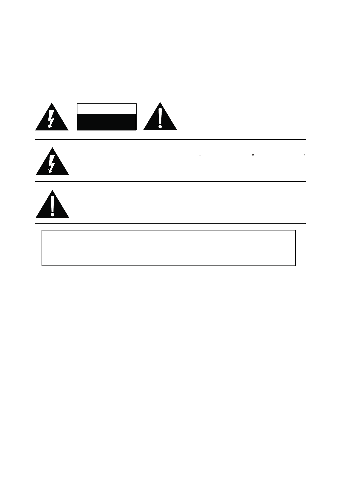
RISK OF
ELECTRIC
SHOCK DO
NOT
OPEN.
SCHNEIDER ELECTRONICS GMBH-GERMANY
1. CAUTION
CAUTION:
Use of controls, adjustments or procedures other than those specified herein may result in
hazardous radiation exposure.
CA UTION : TO RE DUCE THE RIS K OF
CA U T IO N
RISK
SHOCK
The lighting flash with arrowhead symbol, with an equilateral triangle is intended to
alert the user to the presence of uninsulated voltage within the product s
enclosure that may be of sufficient magnitude to constitute a risk of electric shock to
the person.
The exclamation point within an equilateral triangle is intended to alert the user to the
presence of important operating and maintenance (servicing) instructions in the
literature accompanying the appliance.
ELECTRI
NOT
OPEN.
ELECTR ICAL SH OCK, DO NOT REMOVE
COVER (OR BACK). NO USER SERVICEABLE
PAR TS INS IDE . RE FER SER VIC ING TO
QUALIFIE D SERVIC E PERS ONNEL.
dangerous
WARNING: TO REDUCE RISK OF FIRE OR ELECTRIC SHOCK, DO NOT
EXPOSE THIS APPLIANCE TO RAIN OR MOISTURE.
2
2
Page 3

SCHNEIDER ELECTRONICS GMBH-GERMANY
IMPORTANT SAFETY INSTRUCTIONS
CAUTION:
Read all of these instructions. Sa ve these instructions for later use . Follo w all Warnings and
Instructions marked on the audio equipment.
1. Read Instructions-All the safety and operating instructionsshouldbe read before the productis operated.
2. Retain Instructions- The safety and operating instructions should be retained for future reference.
3. Heed Warnings- All warnings on the product and in the operating instructions should be adhered to.
4. Follow Instructions- All operating and use instructions should be followed.
FOR YOUR PERSONAL SAFETY
1. When the power cord or plugis damaged or frayed, unplug this television set from the wall outlet and refer servicing to
qualified service personnel.
2. Do not overload wall outlets and extension cords as this can result in fire or electric shock.
3. Do not allow anything to rest on or roll over the power cord, and do not place the TV where power cord is subject to
traffic or abuse. This may result in a shock or fire hazard.
4. Do not attempt to service this television set yourself as opening or removing covers may expose you to dangerous
voltage or other hazards. Refer all servicing to qualified service personnel.
5. Never push objects of any kind into this television set through cabinet slots as they may touch dangerous voltage
points or short out parts that could result in a fire or electric shock. Never spill liquid of any kind on the television set.
6. If the television set has been dropped or the cabinet has been damaged, unplug this television set from the wall outlet
and refer servicing to qualified service personnel.
7. If liquid has been spilled into the television set, unplug this television set from the wall outlet and refer ser vicing to
qualified service personnel.
8. Do not subject your television set to impact of any kind. Be particularly careful not to damage the picture tube surface.
9. Unplug this television set from the wall outlet before cleaning. Do not use liquid cleaners or aerosol cleaners. Use a
damp cloth for cleaning.
10.1. Do not place this television set on an unstable cart, stand, or table. The television set may fall, causing serious injury
to a child or an adult, and serious damage to the appliance. Use only with a car t or stand recommended by the
manufacturer, or sold with the television set. Wall or shelf mounting should follow the manufacturer s instructions, and
should use a mounting kit approved by the manufacturer.
10.2. An appliance and cart combination should be moved with care. Quick stops, excessive force, and uneven surfaces
may cause the appliance and cart combination to overturn.
3
3
Page 4
SCHNEIDER ELECTRONICS GMBH-GERMANY
PROTECTION AND LOCATION OF YOUR SET
11. Do not use this television set near water ... for example, near a bathtub, washbowl, kitchen sink, or laundry tub, in a
wet basement, or near a swimming pool, etc.
Never expose the set to rain or water. If the set has been exposed to rain or water, unplug the set from the wall
outlet and refer servicing to qualified service personnel.
12. Choose a place where light (artificial or sunlight) does not shine directly on the screen.
13. Avoid dusty places, since piling up of dust inside TV chassis may cause failure of the set when high humidity persists.
14. The set has slots, or openings in the cabinet for ventilation purposes, to provide reliable operation of the receiver, to
protect it from overheating. These openings must not be blocked or covered.
Never cover the slots or openings with cloth or other material.
Never block the bottom ventilation slots of the set by placing it on a bed, sofa, rug, etc.
Never place the set near or over a radiator or heat register.
Never place the set in enclosure, unless proper ventilation is provided.
a built-in
PROTECTION AND LOCATION OF YOUR SET
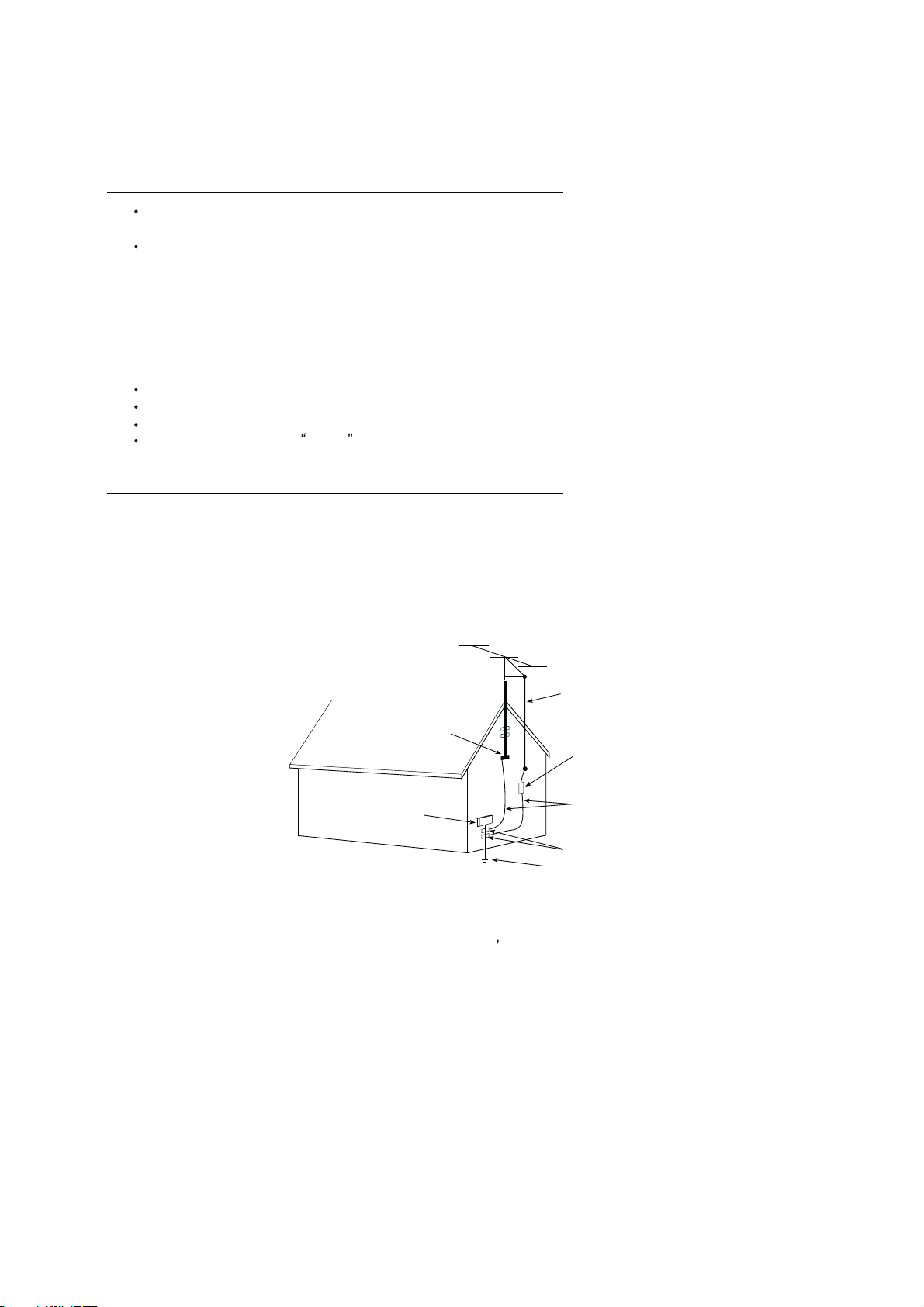
15.1. If an outside antenna is connected to the television set, be sure the antenna system is grounded so as to provide some
protection against voltage surges and built up static charges, Section 810 of the National Electrical Code, NFPA No.
70-1975, provides information with respect to proper grounding of the mast and supportingstructure, grounding of the
lead-in wire to an antenna discharge unit, size of grounding conductors, location of antenna discharge unit, connection
to grounding electrode, and requirements for the grounding electrode.
EXAMPLE OF ANTENNA GROUNDING AS PER NATIONAL ELECTRICAL CODE INSTRUCTIONS
EXAMPLE OF ANTENNA GROUNDING AS PER
NATIONAL ELECTRICAL CODE
ANTENNA
LEAD- IN WIRE
GROUND CLAMP
ELECTRIC SERVICE
EQUIPMENT
NEC-NATIONAL ELECTRICAL CODE
ANTENNA DISCHARGE
UNIT (NEC SECTION
810-20)
GROUNDING
CONDUCTORS
(NECSECTION 810-21)
GROUND CLAMPS
POWER SER VICE GROUNDING
ELECTRODE SYSTEM
(NEC ART 250. PART H)
15.2. Note to CATV system installer : (Only for the television set with CATV reception)
This reminder is provided to call the CATV system attention to Ar ticle 820-40 of the NEC that provides
installer s
guidelines for proper grounding and, in particular, specifies that the cable ground shall be connected to the grounding
system of the building, as close to the point of cable entr y as practical.
16. An outside antenna system should not be located in the vicinity of overhead power lines or other electric lights or power
circuits, or where it can fall into such power lines or circuits. When installing an outside antenna system, extreme care
should be taken to keep from touching such power lines or circuits as contact with them might be fatal.
17. For added protection for this television set during a lightning storm, or when it is left unattended and unused for long
periods of time, unplug it from the wall outlet and disconnect the antenna. This will prevent damage due to lightning
and power-line surges.
4
4
Page 5

SCHNEIDER ELECTRONICS GMBH-GERMANY
OPERATION OF YOUR SET
18.
This television set should be operated only from the type of power source indicated on the marking label.If you are not
sure of the type of power supply at your home, consult your television dealer or local power company. For television
sets designed to operate from battery power, refer to the operating instructions.
19. If the television set does not operate normally by following the operating instructions, unplug this television set from the
wall outlet and refer servicingto qualifiedservice personnel. Adjust only those controls that are covered in the operating
instructions as improper adjustment of other controls may result in damage and will often require extensive work by a
qualified technician to restore the television set to normal operation.
20. When going on a holiday : If your television set is to remain unused for a period of time, for instance, when you go on
a holiday, turn the television set and unplug the television set from the wall outlet.
off
IF THE SET DOES NOT OPERATE PROPERLY
21. If you are unable to restorenormal operation by followingthe detailedprocedurein your operatinginstructions,
do not attempt any further adjustment. Unplug the set and call your dealer or service technician.
22. Whenever the television set is damaged or fails, or a distinct change in performance indicates a need for
service, unplug the set and have it checked by a professional service technician.
23. It is normal for some TV sets to make occasional snapping or popping sounds, particularly when being
turned on or off. If the snapping or popping is continuous or frequent, unplug the set and consult your
dealer or service technician.
FOR SERVICE AND MODIFICATION
24. Do not use attachments not recommendedby the television set manufacturer as they may cause hazards.
25. When replacement parts are required,be sure the service technicianhas used replacementparts specified
by the manufacturer that have the same characteristics as the original part. Unauthorized substitutions
may result in fire, electric shock, or other hazards.
26. Upon completion of any service or repairs to the television set, ask the service technician to perform
routine safety checks to determine that the television is in safe operating condition.
5
5
Page 6
PRODUCT SPECIFICATION RELEASE
AC 100V-240V 50/60H
p()
Screen Mode
16:9\4:3\14:9\Cinerame\Zoom etc
Audio Delay
Yes
!
Model: 48D2700/MT56B/CS1GTA/TT E5
Model: 48D27
Version:1.0 Issued On: 2015-05-12
Basic Information
Product Type
Chassis
CPU Quad Core A7 1GHz Mutilmedia Video/Audio Decoder
GPU Dual Core MALI450MP2 400MHz
OS Android 4.4
Memory/Flash 6Gb DDR3 / 4GB Flash
UI Style CROSS UI
Launcher HomePages Show
OSD Language English/Vietnamese/Thai
TV System
AV System
Channels
Power Supply
Power Consumption(TV On)
Power Consumption(Standby)
Certification
ECO Energy efficiency
Internet Link
LED Indicator Status In The Center of Front,White in Standby
LED 2D Smart DTV
MT56B
APPS、TV、GOLIVE、YouTube
PAL B/G、D/K、I;NTSC-M; DVI Video Format Up to XGA for HDMI-PC
DVB-T/T2 HDMI Video Format up to 1080P
PAL、NTSC
0000-9999
z
110W
≤0.5W
CB
Yes Aspect Ratio 16:9
wireless WiFi Default Panel Active Size (inch) 48
Ethernet Network
Basic Function
Initial Setup
HDMI Auto Switch Auto、Close、Manual Life Time(Typ.) 30,000hrs
Channels Edit For Channel renamed
Input Settings For Input source device choice
Sleep Timer Yes
System Update Yes
T-Link(CEC)
Input Method Smart TV IME
MHL Yes
Teletext Yes
Audio Language/Nicam Yes
PVR/Timeshift Yes (Only for DTV Programme)
Programme Schedule Record/Reminder(Only for DTV Programme)
EPG Yes(Only for DTV Programme)
Subtitle Yes(Only for DTV Programme)
Yes,for user setting in TV first starting Viewing Angle (H/V) 178°/178°
Yes
USB Device Media Format
Music MP3
Picture JPEG/BMP/PNG/GIF
MPEG-(1/2/4)/H.264/H.263/DivX Dolby/AC3
Signal Format Capability
PC Compatibility Up to SXGA
Panel Specification
Backlight Unit
Panel supplier CSOT
Display Resolution 1920*1080
Brightness (cd/m2) 280(typ.)
Contrast Ratio 4000:1
Response Time (G to G) 9ms
Color 16.7 Million(8bit)
Refresh Rate 60Hz
LED
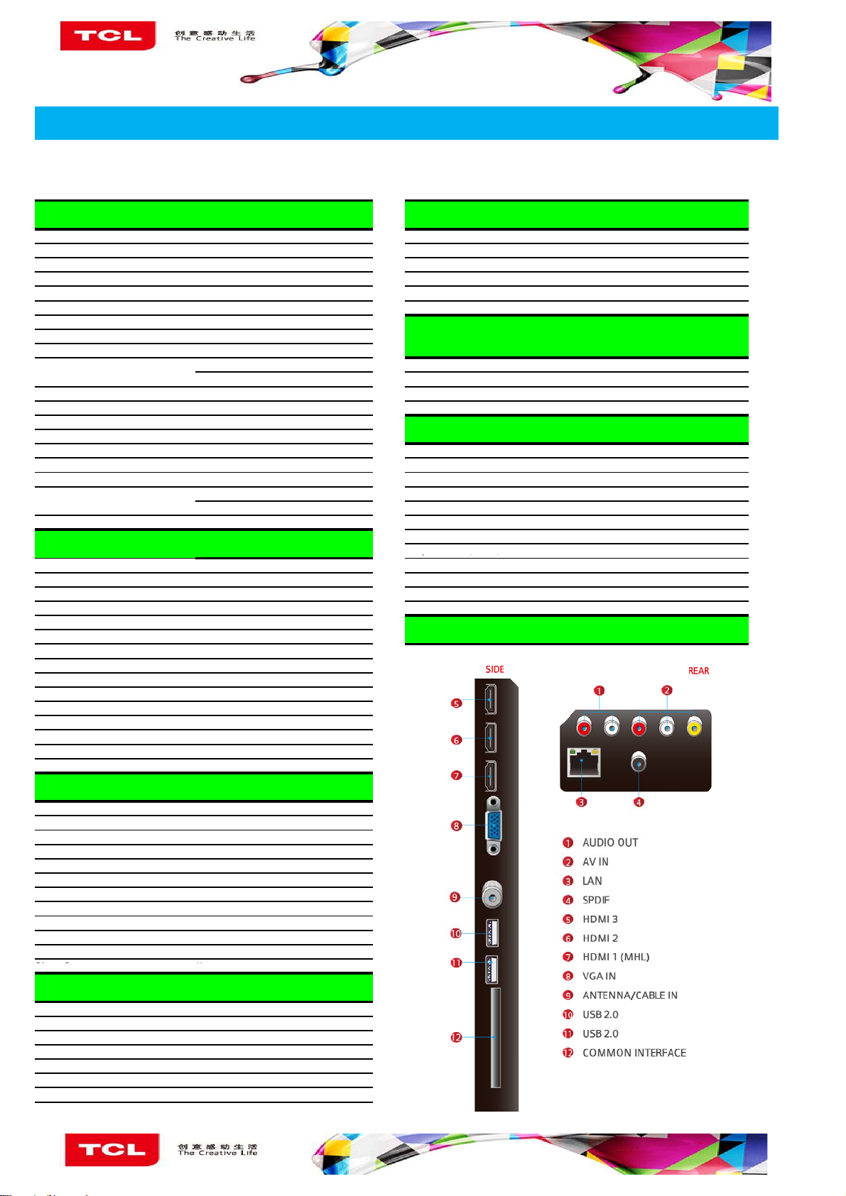
Terminals
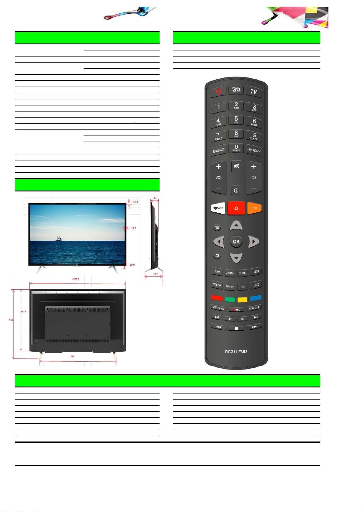
Rearview Picture
Picture
Picture Mode Standard\Dynamic\Natural\Movie\Personal
Screen Mode 16:9\4:3\14:9\Cinerame\Zoom etc.
Noise Reduction Low\Middle\High\Auto\Off
Backlight Adjustable Yes (0~100)
Color Temperature Normal/Warm/Cool/Customer
Gamma Adjustable -4 to 4
Dynamic Contrast Yes
Overscan Yes
Picture Freeze Yes
Game Mode Yes
Film Mode Yes
Picture Reset Yes
.
Sound
Speakers Integrated speakers (Bottom side)
Audio Power Output(THD=7%) 2×8W
Auto Volume Control On / Off
Sound Preset Standard\Music\Movie\Clear Voice\Personal
Sound Control
TV Placement
Five band equalizer adjust in Personal mode
Desk top / Wall mount
Yes
Design and specifications are subject to change without notice
Page 7
Pre-Installed Application List
Wirel
p
YouTube
Golive Lots of Global Live TV channels show
Miracast
App Store 3.0 Special App Store available for download
Browser Webpage Browser
TV Tweets a Social App
Deezer Global Online Music Streaming service
Mediacenter Media/Music play for USB Device
Message Box Messages push
Weather forecast Showed in Homepage
E-Sticker as some function demo in Shop mode
E-Manual Some general basic function introduction
nScreen
Zing TV Vietnam local Popular Video App
Zing mp3 Vietnam local Popular Music App
Independent Launcher UI page show Operation Manual English(Default)
Push Popular VOD posters to Homepage Remote Control and batteries RC311(with two batteries)
ess Mirroring connecting,to deliver audio
and video content from smartphone to TV
Connect Mobile phone to TV sets and control
the TV like Remote using Phone;
Push media file in Phone to TV Display and
Enjoy big screen picture quality.
Mechanical ID Picture
Essential Accessories(Default)
Base Stand
AC power cord 1 pcs
Integrated Packaging
Mechanical Key Specification
L1(mm)
W1(mm)
H1(mm)
L2(mm)
W2(mm)
H2(mm)
Net Weight With Stand(Kg)
Net Weight Without Stand(Kg)
Gross Weight With Packaging(Kg)
1090.8
82
632.5
888
222
683
10
9.75
13.5
Diagonal size(cm)
Slim Edge Design---Up(mm)
Slim Edge Design---Bottom(mm)
Slim Edge Design---L&R(mm)
Carton Dimensions LxWxH(mm)
Container Loading---20 feet(pcs)
Container Loading---40 feet(pcs)
Container Loading--40 feet High(pcs)
VESA Mounting Dimensions LxH(mm)
Drafted by: Approved by:
120.9
16.9
19.6
16.9
1282*154*768
192
411
465
200*200
Page 8

Factory Test & Alignment Specification For MT56-AP Series (V1.0)
TCL World-Wide R&D
FPD CENTER
Factory Test & Alignment Specification V1.0
----MT56-AP
PREPARED BY : FENG LIU DATE : 2015-02-13
APPROVED BY: DATE :
1
Page 9

Factory Test & Alignment Specification For MT56-AP Series (V1.0)
Content
1. General Description .............................................................................................................................. 3
2. Factory Menu ......................................................................................................................................... 5
2.1 Accessing Way ................................................................................................................................... 5
2.2 Factory Menu ...................................................................................................................................... 6
2.3 White Balance Menu .......................................................................................................................... 7
3. Design Menu .......................................................................................................................................... 7
3.1 Accessing Way ................................................................................................................................... 8
3.2 Design Menu ....................................................................................................................................... 8
3.3 Other Menu ......................................................................................................................................... 9
3.4 Service Menu ...................................................................................................................................... 9
3.5 Param Setting Menu ........................................................................................................................ 10
4. Test & Alignment ................................................................................................................................. 11
4.1 Pre-Conditions and Power Supply Check .................................................................................... 11
4.2 Project ID Modification .................................................................................................................... 11
4.3 Function Test .................................................................................................................................... 12
4.4 LAN/WLAN Test ............................................................................................................................... 13
4.5 SHOP INIT ........................................................................................................................................ 13
Appendix ...................................................................................................................................................... 14
Appendix 1: Warm-up Test .................................................................................................................... 14
Appendix 2: Software Upgrade ............................................................................................................. 15
Appendix 3: Network Connection ......................................................................................................... 17
Appendix 4: White Balance (WB) Adjustment .................................................................................... 18
2
Page 10
Class
Item
MT56-AP
Input
&
Output
RF Input
(PAL/DVB/DVB-T2)
CABLE&ANTENNA
HDMI
(480i/p, 576i/p, 720p up to 1080i/p, with
HDCP)
HDMI*3
VGA
1
VGA Audio
Shares audio sockets with Audio Input
Component Audio Input
RCA*2 (L+R)
AV Input
RCA*1
Factory Test & Alignment Specification For MT56-AP Series (V1.0)
1. General Description
The information contained in this document is proprietary to TCL SZ FPD lab and shall
not be disclosed by the recipient to the third person without the written permission of
the team leader or GM of R&D.
MT56-AP chassis are designed for Asia & Pacific (AP) market Ready for Smart TV. It
features by its high integration, easy debugging (ADC adjustment free) as well as
convenience in terms of maintenance. Fast software upgrade through USB disk
facilitates both manufacture and after-sale service. Meantime, a variety of functions
involved in Factory Main Menu can not only bring benefits for production, but also
satisfy various demands of customers.
Note: Factory Main Menu (FMM) is divided into Factory menu and Design menu. Factory
Menu covers all indispensable functions during manufacture such as White Balance
Adjustment, SHOP etc., while Design Menu includes Service Menu, Hotel Menu, Param
Setting, Other Setting etc. Some settings like Param Setting and Other Setting is exclusively
used by R&D engineer, anyone else shouldn’t change the settings in the menu. When you
wish to learn the product information like project ID, project name, Hardware, software
version, release date, you can access to Service Menu. In addition, in Hotel Menu, we also
provide a great deal of useful functions for specific applications in hotel.
The main chip is from REALTEK and supports below features matrix:
3
Page 11
Input
&
Output
Audio Out
RCA*2
USB
(Video, audio and picture)
USB2.0*2
MHL
Shares with HDMI 1
PCMCIA
1
SPDIF output
RCA*1
NETWORK
RJ45 Socket
Functions
Internet
WIFI
Others
Serial connector
Multiplexing VGA
IC Details
&
Position
Main program
UF01
(Support online upgrade)
Mboot
UF01
(Support online upgrade)
EEPROM
U702
Factory Test & Alignment Specification For MT56-AP Series (V1.0)
Note:
The software boot for U702 can be programed by Flash Tool.exe.
Every set has its unique HDCP key which is purchased from suppliers or HDCP
certification authority. Please check HDCP function in the process of production.
Once in a while, the software of main board may be upgraded. Please pay attention to
use the latest software before production.
4
Page 12
Factory Test & Alignment Specification For MT56-AP Series (V1.0)
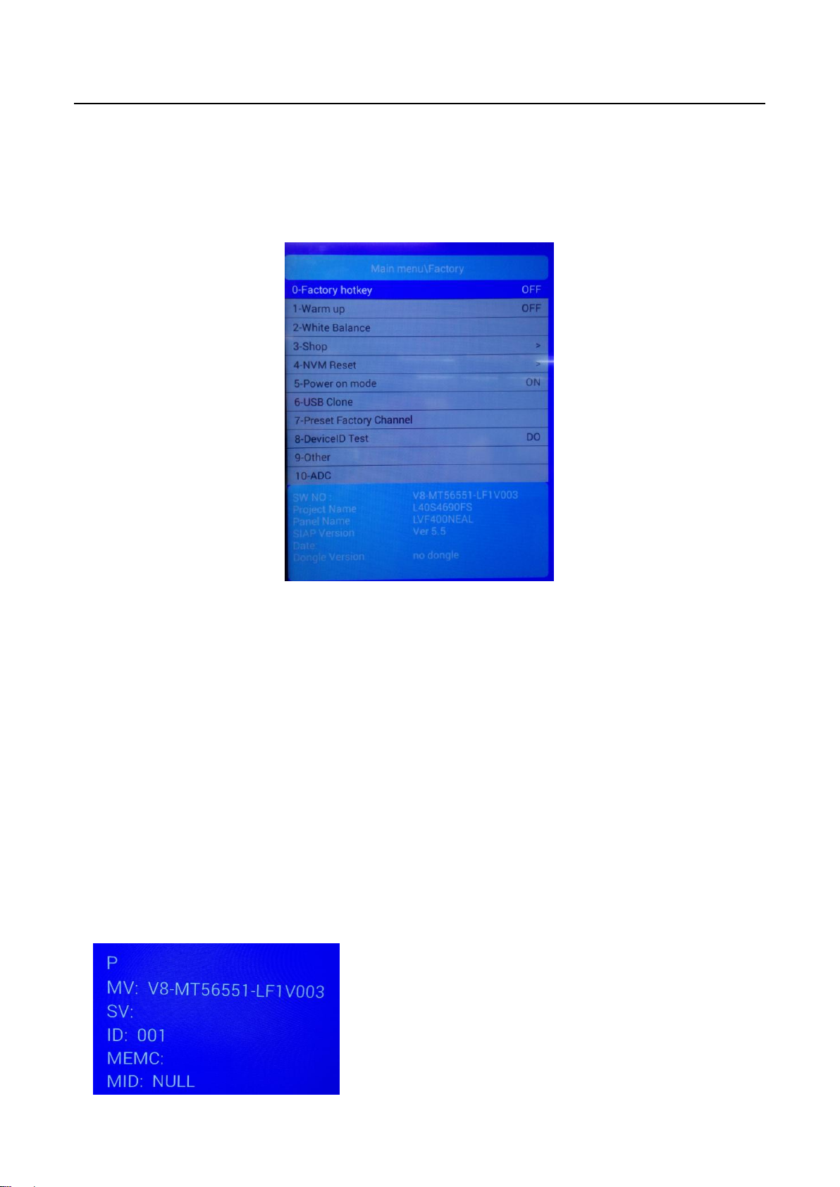
2. Factory Menu
Factory Menu is mainly used for factory production and satisfies various demands of customers. It covers
all indispensable functions during manufacture such as Warm up, White Balance, Shop, NVM Reset,
Power on mode, USB Clone etc.
2.1 Accessing Way
a. When the Factory hotkey item of Factory Menu is disabled (OFF), press Menu button of remote
control, then select Settings/Picture, make sure the cursor stop on Contrast item submenu. Finally,
press 9, 7, 3, 5 consecutively.
b. When the Factory hotkey item of Factory Menu is enabled (ON, you can see the flashing Factory
Captions Info on the lower left corner), press Back button of remote control.
Press RCU “OK” key to enter the submenu.
Press RCU “Right” or “Left” key to change the values.
Press RCU “Right” or “Left” key run the function.
Press RCU “Back” or “Menu” key exit the Factory menu.
Factory Captions Info:
While “FactoryKey” is enabled, there is some toggled display information relative to MV, SV, ID, MID, to
facilitate 100% quick screening without accessing to whatever else menu:
P (Production/Factory mode flag)
MV (Mboot SW Version)
SV (Main SW Version)
ID (Project ID)
MEMC
5
Page 13
Factory Test & Alignment Specification For MT56-AP Series (V1.0)
Factory Menu
Name
Default
Description
Factory hotkey
OFF
Factory Menu shortcut button switch
The item must be disabled (OFF) after production
Warm up
OFF
Aging mode, mainly used for factory aging.
Press “Menu” key on keyboard to exit the burning mode.
See Appendix 1 “Warm-up Test”
White Balance
..
White Balance Adjustment ( see details below)
Shop
>
It is crucial that the function is executed after production aim to clear information
of production process, ensure user cannot access to Factory Menu after
executing the item.
NVM Reset
>
Restore default value except White Balance, ADC data.
Power On Mode
STANDBY
ON: the set will power on after switching on power.
STANDBY: the set will remain standby status after switching on power.
LAST: the set will turn to the status in which it lies when last switching off.
If without requirement from certain customer, by default, the Setting should be
STANDBY
USB Clone
..
Select to choose the things you want to clone.
Preset Factory
Channel
..
Preset the channel table of factory. To preset the channel table of certain factory,
first, choose the corresponding factory name. Then press OK button of remote
control and wait OK is displayed on the screen.
DeviceID test
DO
Test device ID.
Other
Project Information
ADC
..
Analog To Digital Converter
SW NO.
device info
Version information of Main Software
Project Name
device info
Product model
Date
device info
Release date and time of main software
MID
2.2 Factory Menu
6
Page 14
White Balance
Name
Default
Description
Source
ATV
Press RCU left/right key to change the TV source.
Color
normal
Select color temperature you intend to adjust Three groups of color
temperature: normal, Cold, Warm are available.
R gain
0-255
Gain of R channel ( cannot be changed after auto calibration)
G gain
0-255
Gain of G channel ( cannot be changed after auto calibration)
B gain
0-255
Gain of B channel ( cannot be changed after auto calibration)
R offset
128
Disabled, keep the default value
G offset
128
Disabled, keep the default value
B offset
128
Disabled, keep the default value
White Balance
init
>
White Balance Initalization. Before WB adjustment, this item should be
executed.
Factory Test & Alignment Specification For MT56-AP Series (V1.0)
2.3 White Balance Menu
Press the button on remote control to select certain item and OK to adjust White Balance.
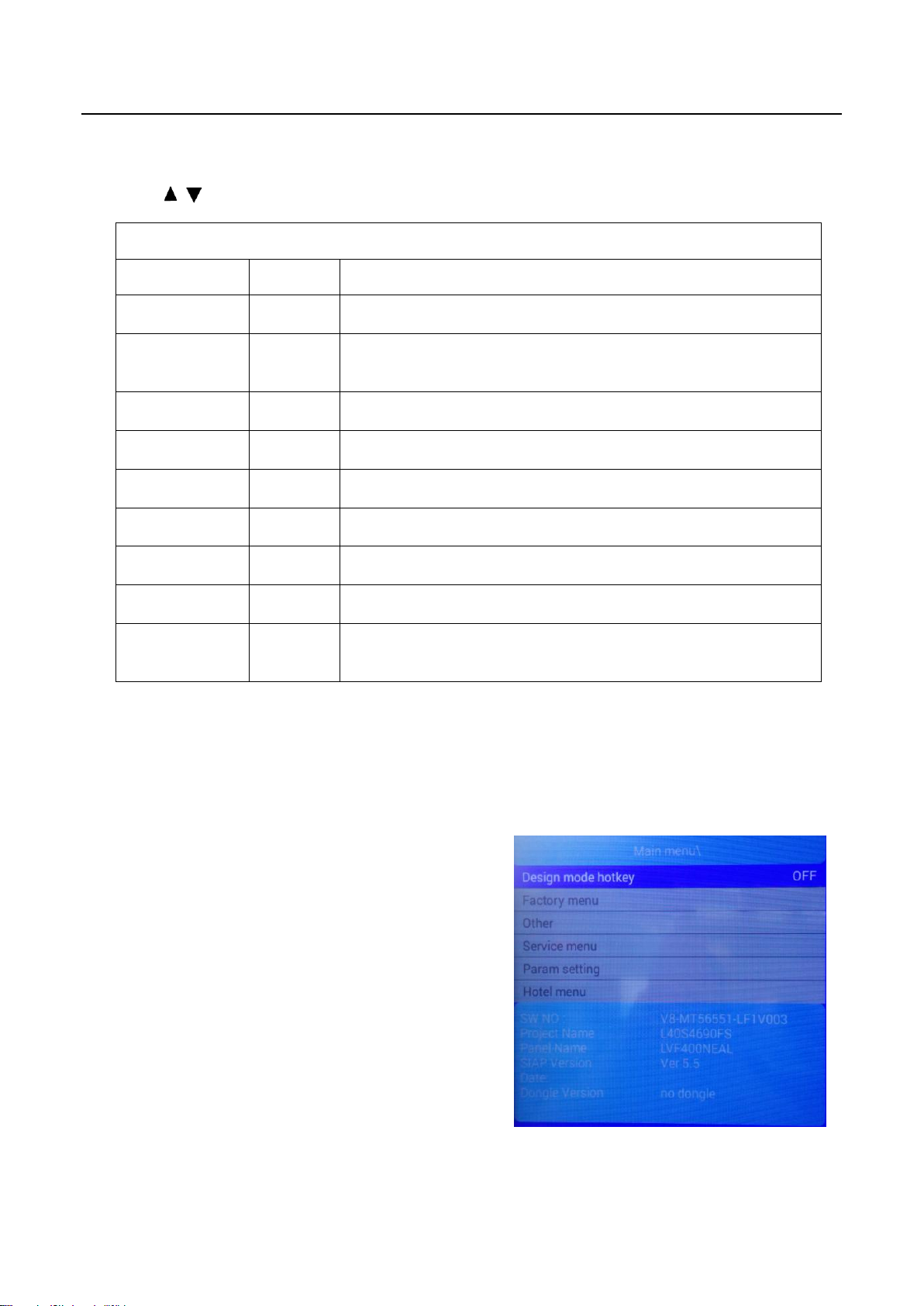
3. Design Menu
Design Menu includes Factory Menu, other,
Service Menu, Param Setting, Hotel Menu.
Some settings like Param Setting and Other
Menu is exclusively used by R&D engineer,
anyone else shouldn’t change the settings in the
menu. When you wish to learn the product
information like project ID, project name, chassis
name, software version, release date, you can
access to Service Menu. In addition, in Hotel
Menu, we also provide a great deal of useful
functions for specific applications in hotel.
7
Page 15
Design Menu
Name
Default
Description
Design Mode
hotkey
OFF
Design Menu shortcut button switch
The item must be disabled (OFF) after production
Factory menu
..
Access to Factory Menu
Other
..
The item includes a number of functions offering convenience for R&D engineer
to solve problems.
Service menu
..
Provide many useful information for after-sale service
Please reference to SERVICE MENU submenu
Param setting
..
Include sound setting,picture setting, SSC, DBC, CI Card, Overscan, WIFI
CHECK and USB FILE. Please reference to PARAM SETTING submenu.
Hotel menu
..
Include special functions which bring benefits to hotel management. The item is
accessible only when Hotel Service On/Off item is enabled (ON).
Factory Test & Alignment Specification For MT56-AP Series (V1.0)
3.1 Accessing Way
a. When the Design mode hotkey item is disabled(OFF), press Menu button of remote
control, then select Settings/ Picture, make sure the cursor stop on Contrast item
submenu, press 1, 9, 5, 0 consecutively.
b. When the Design mode hotkey item of Design Menu is enabled (ON, you can see the
flashing Factory Captions Info on the lower left corner), press Back button of remote
control.
Press RCU OK key to enter the submenu.
Press RCU Right/Left key to change the values.
Press RCU Right/Left key run the function.
Press RCU Back/Menu key exit the Factory menu.
Design Captions Information is the same to Factory Captions Info.
3.2 Design Menu
8
Page 16
Other Menu
Name
Default
Description
TestPattern
>
Switch the TV source into test pattern, and restarting TV is the only way to excit.
UartEnable
OFF
The switch of VGA serial port information.
The item must be disabled (OFF) after production.
DeviceID
..
Show the device id of TV.
MAC
..
Show the MAC address of TV.
HuanID
..
Show the Huan id of TV.
ClientType
..
Show the Client type information.
Service Menu
Name
Default
Description
Project ID
1
Select project parameters, depending on the BOM description.
Hardware
MT5655
mainboard Chassis
Software
V8-MT56551-LF1V003
version number of Main Software
Bootloader
XXX
version number of bootcore
USB Update
..
Update the software by USB disk,
detailed description see Appendix 2 “Software Update”
Factory Test & Alignment Specification For MT56-AP Series (V1.0)
3.3 Other Menu
The Other Menu contains some TV basic information, with which we can check the TV setting before
production.
3.4 Service Menu
Service Menu contains some basic information of the device, such as Project ID, Hardware, Software
version, USB Update etc. This menu is especially useful for after-sale service.
9
Page 17

Param setting Menu
Name
Default
Description
Sound Setting
..
Set sound mode, balance, sound scene, etc.
Picture Curve
..
Exclusively used by R&D
Picture Setting
..
Set picture mode, brightness, contrast, backlight, etc.
SSC Adjust
..
Spread Spectrum clocking.
Exclusively used by R&D.
DBC
..
Dynamic Backlight Control.
Exclusively used by R&D.
CI Card
ON
Common interface Card switch.
WIFI CHEAK
..
Check the WIFI link
USB FILE
..
Access the USB file
Factory Test & Alignment Specification For MT56-AP Series (V1.0)
3.5 Param Setting Menu
Param Setting menu contains Sound Setting, Picture Curve, Picture Setting, SSC, DBC, CI Card,
Overscan, WIFI CHECK and USB FILE. But it is exclusively used by R&D engineer, anyone else shouldn’t
change the settings in the menu.
10
Page 18

Position
Value
Test Point
P103
12V±10%
12V
LDH1
5V±5%
+5V
P103
3.3V ±1%
3V3SB
UD33
3.3V ±1%
3V3
LDJ1
1.5V ±1%
DDR_1V5
LDB0
1.2V±1%
CORE_1V2
UD18
1.8V ±1%
1V8
UT2
3.3V ±1%
TUNER_VCC
U201
3.3V ±1%
3V3_DEMO
L201
1.1V ±1%
NC
Factory Test & Alignment Specification For MT56-AP Series (V1.0)
4. Test & Alignment
According to the requirement of order, we suggest take the below steps to finish the appropriate settings.
Note:
All tests and measurements mentioned hereafter have to be carried out at a normal mains voltage
(100 ~ 240 VAC)
All voltages have to be measured with respect to ground, unless otherwise stated
All final tests have to be done on a complete set including LCD panel in a room with temperature of
25+/-7°C
The Picture Performance assessment such as White Balance (luminance and colour temperature)
has to be performed into subdued lighted room after at least 60min of warm-up in order to avoid any
temperature drift influence (colorimetry vs time).
4.1 Pre-Conditions and Power Supply Check
Before power-on, please check the board according to the relevant block diagram and circuit diagram,
make sure that no serious issue or mistake can destroy the board. For example, the output of DC/DC and
LDO should not be shorted to ground.
Supply a suited voltage and power-on, then check the voltage according to the relevant block diagram,
circuit diagram and voltage spec, the error should be less than 5%, for example, the voltage for main chip
(+3V3, +2.5V, VDDC1V15, 1V5_DDR, etc.), the voltage for TUNER (TU_3V3), the voltage for amplifier
(AMP_VCC), etc.
4.2 Project ID Modification
There are different ID stored in the EMMC depending on different Panels settings and Model features, but
there’s only one key branching Project ID able to ensure normal display. And when you power on the TV
set, you should make sure the Project ID is accord with the BOM description. If not, you need to modify
11
Page 19
MODEL
ProjectID
Panel Name
L40S4690FS
001
LVF400NEAL
Source
Test Signal
Test Pattern
RF Input
(PAL/DVB/DVB-T2)
RF cable
Factory signal
AV
(CVBS)
Chroma/Fluke generator
PAL Half Color & Gray bars
VGA
Chroma/QuantumData
generator
1024x768@60Hz
Half Color & Gray bars
HDMI
(Video & Audio)
DVD with HDMI compliancy
Movie 720p@60Hz
LAN
(RJ45)
Ethernet
Any network
Audio OUT
RF signal
Suitable channel
USB
Video/MP3/Image
Home/Media/
SPDIF
DOSS
Audio output
PCMCIA
TV source
Suitbale PCMCIA Card
Factory Test & Alignment Specification For MT56-AP Series (V1.0)
the ID. There are two methods to modify the ID:
Change Project ID in Design Menu
In case of “Design mode hotkey” is enabled, press “Back” button to enter Design Menu. To modify
Project ID, you need to go through “Service menuProject ID”, then press Left or Right key to
select suitable ID (Project name is dynamically refreshed). Finally restart the TV set.
In case of “Design mode hotkey” is unabled, you can enter the Design Menu easily with reference
to 3.1 Design Menu.
Change Project ID with RCU
Press “062598”+”Menu”+”XXX” (XXX represents project ID you’d like to switch to) in the remote
control and wait about half minutes, When the set restart automatically, you have successfully
changed project ID.
Here below is none exhaustive ProjectID table for reference:
4.3 Function Test
Once the Project ID is correct and the TV display normally, plug all external generator devices to relevant
inputs/outputs below according to their respective test patterns format and check picture content and
sound quality accordingly:
12
Page 20

Device ID
User ID
2bbf5dec37068855003ef54b9e27f3be68118899
3546187
Factory Test & Alignment Specification For MT56-AP Series (V1.0)
4.4 LAN/WLAN Test
MAC Address Upgrade
Upgrading MAC address needs to use the tool in factory and through serial command. The specific
method is according to the operation of the factory guidance.
DeviceID (DID) and UserID (UID)
Purpose is to allow Other Network Download (OND) and further specific services over dedicated portal
based on AP. For such, specific DID (32 bytes) and UID (8 bytes) needs to be paired and overwritten into
memory for internal client encryption,as below:
Those DID/UID codes can only be set using UART commands following enclosed SIACP requirements
(rev. v3.9).
LAN Test
A rough LAN test can be done by connecting Ethernet to TV’s RJ45 and check that IP, subnet mask, DNS
addresses, which are visible on “HomeSettingsNetworkEthernet settingsIP settings” (ensure
that “Internet Connection” is Enabled at first). More in-depth test can be performed faster using suitable
UART/IR commands following SIACP requirements. SW will internally manage Network ID (NID) flag
controlling all MAC/DID/UID integrity to facilitate PA screening further.
See Appendix 3 “Network Connection”
4.5 SHOP INIT
At final process stage, it’s necessary to perform Shop init before any packing to leave Factory mode and
restore User default presets according to the requirement of order.
This function is accessible by selecting “Factory MenuShop”, then pressing RCU “Right ”or” Left” key.
Other faster methods are available on above enclosed SIACP requirements (rev. v3.9).
13
Page 21

Factory Test & Alignment Specification For MT56-AP Series (V1.0)
Appendix
Appendix 1: Warm-up Test
Following TCL standard and practices, it’s required minimum 15min of Warm-Up that can be considered
as Burn-In. Additional aging for White Balance alignment is no more necessary due to consistent picture
performance with cloning usage. This function is accessible by selecting “Factory menu Warm up”,
pressing RCU “Right” or ”Left” key to set it ON, and then it enter in Warm up mode. Press “Menu” key on
keyboard to exit the burning mode. Other faster methods are available on above enclosed SIACP
requirements (rev. v3.9).
14
Page 22
Factory Test & Alignment Specification For MT56-AP Series (V1.0)
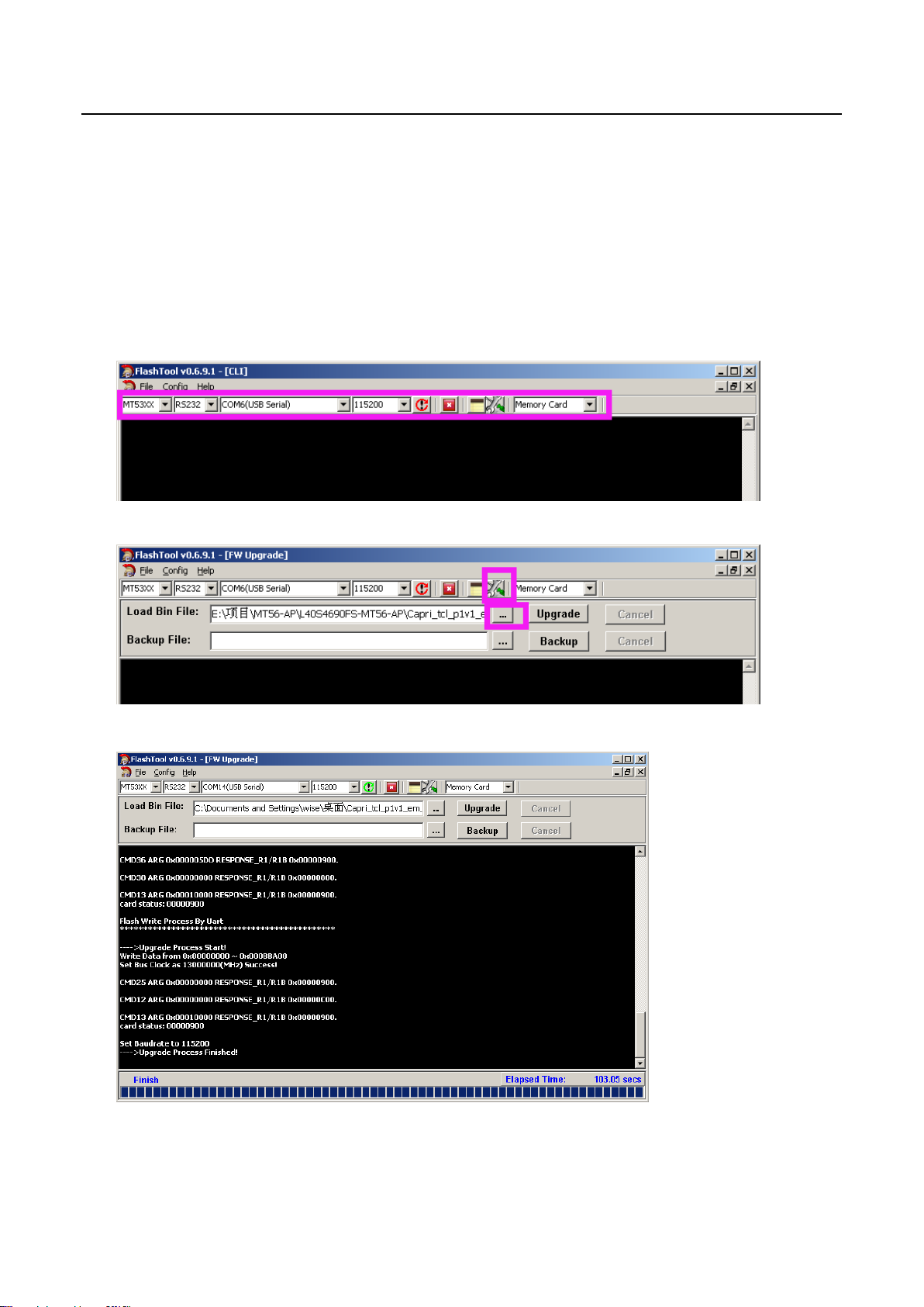
Appendix 2: Software Upgrade
How to upgrade Mboot
Connect the computer and mainboard VGA port by a serial port tool.
Serial connector definition: VGA/P303: Pin4: RXD VGA Pin11:TXD
Open MTK “Mboot” software programming tool “Flash Tool”, and set serial port.
Import the mboot file, as below.
power on the TV, then Click Upgrade key and you will see the below message.
15
Page 23

Factory Test & Alignment Specification For MT56-AP Series (V1.0)
How to upgrade FLASH Software
1. USB Upgrade
Download the update file (generally named V8-MT56551-LF1VXXX.pkg) to the root directory of your
USB device, and make sure there’s no other bin file named analogously. Then insert the USB device
to USB interface of TV set.
Power on the TV set, Press and hold on the menu key of key board at the same time. If the TV is
updating, you’ll see the below screen:
Upgrade process takes about 3~5 minutes.
After updating, the TV set will reset automatically.
2. Online Upgrade
Download the bin zip file “V8-MT56551-LF1VXXX.Zip” to the root directory of your USB device, and
do not change the file name. Then insert the USB device to USB interface of TV set.
Press RCU Menu/Settings/Picture/Contrast/1,9,5,0/Service menu/USB Update /Main
Upgrade/Local Update . If the upgrade file is found, TV will give a message that it verifying. TV
displays a warning message, it means selecting “confirm” to continue or “cancel” to exit. During
updating, do not power off the TV set.
After updating, the TV set will reset automatically.
16
Page 24

Factory Test & Alignment Specification For MT56-AP Series (V1.0)
Appendix 3: Network Connection
You can set up your TV so that it can access the Internet through your local area network (LAN) using a
wired or wireless connection.
Connect to a wired network
Attach the TV set to your LAN using cable in three ways:
Connecting the LAN port on the TV to an external modem using a Cat 5 cable.
Connecting the LAN port on the TV to an IP Sharer which is connected to an external modem. Use
Cat 5 cable for the connection.
Depending on how your network is configured, you may be able to attach the TV to your LAN by
connecting the LAN port on your TV directly to a network wall outlet using a network cable. Note that
the wall outlet is attached to a modem or router anywhere in your house.
Select Home→ Settings→ Network → Ethernet Settings→IP Settings, then the TV will obtain IP
address Automatic configuration. In addition, you can set the IP address and password manually.
Connecting to a wireless network
To connect the TV set to your network wirelessly, you need a wireless router or modem and a Wireless
LAN Adapter.
If the TV set is equiped with an internal WiFi module, select Home→ Settings→ Network→ Wireless
Settings, then turn on Wireless Switch, select a wireless network and press OK to connect.
If you want to connect the TV set to a wireless network by a Wireless High Gain USB Adapter (USB
dongle), select Home→ Settings→ Network→ Wireless Settings, then turn on Wireless Switch and
External WiFi, and select a wireless network and press OK to connect.
17
Page 25

Product
type
Color
temperature
state
Color
temperature
chromaticity coordinate
tolerance
(X,Y)
X
Y
LCD
cold
13000K
0.270
0.270
±0.015
normal
10000K
0.280
0.290
warm
7500K
0.300
0.305
source
HDMI
VGA
AV/ATV
CMP
Timing value
69
14
38
79
Pattern value
103
103
103
103
Factory Test & Alignment Specification For MT56-AP Series (V1.0)
Appendix 4: White Balance (WB) Adjustment
The White Balance generally is customized by PQ engineer, and uploaded to the PDM system, anyone
else shouldn’t change the value in the menu. If it is necessary to adjust, the following content can offer
some reference, but the process of adjusting White Balance is out of the range of this file. Please refer to
the relevant technical file of HuiZhou factory of TCL.
Calibration of Color Temperature
According to TCL standards, the color temperature and white reference coordinates of LCD like the
following table: (This standard is based on CA-310 color temperature meter)
White balance adjustment takes the Normal color temperature of HDMI channel as the reference.
Warm and Cold tone is relative to Normal mode. The adjustable gain range is 0~255.
The Normal color temperature of other channel is relative to the Normal mode of HDMI channel. The
adjustable gain range is also 0~255.
The manual adjustment is according to the regulation above. Additionally, when manually adjust, it
needs to do White Balance init first.
Take signal generator 22293 as an example, the timing value and pattern value of each source show in
the following table:
Note: 1) The input signal is 80% white when the pattern value of 22293 is 103.
2) The adjustment of White Balance should fulfill TCL matching specification.
18
Page 26
5
4
3
2
1
12V
Power ON
D D
12V
12V
Power ON
5V
5V 3V3_Normal
C C
5V TU_3V3
5V 3V3_DEMO
5V 1V1_DEMO
3V3 1V8
B B
5V MHL_5V
3V33B
CORE_1V2
3V3
3V3
1V8
12V
3V3
Power ON
A A
3V3_DEMO
1V1_DEMO
3V3_Normal
1V8
DC_IN
EN
DC_IN
DC_IN DC_OUT
EN
DC_IN DC_OUT
DC_IN DC_OUT
DC_IN DC_OUT
DC_IN DC_OUT
DC_IN DC_OUT
DC_IN DC_OUT
DC_IN DC_OUT
AVDD33_STB
CORE_1V2
VCC
AVDD33
VCC_EMMC
+12V
+3.3V
EN
VDD33C
CVDD
33V_NORMAL
1.8V
DC_OUT
TPS56528
DC_OUT
TPS560200
MP8765
RT8096A
AS1117-3.3
AS1117-3.3
AS1117-3.3
RT8096A
AS1117-1.8
G524
MT5655
AD82587D
ATBM7811
EMMC
UD4
U101
UDB0
U104
UD33
UT2
U201
U202
UD18
U404
max 5A
max 500mA
max 6A
max 1A
max 1A
U001
U801
UM3
U701
5V
3V3SB
CORE_1V2
DDR_1V5
12V
12V
1510mA
GPIO
350mA
POWER_ON
POWER_ON
POWER_ON
12V_IN 12V_OUT
EN
SWITCH
DC_IN
EN
DC_IN
EN
12V
EN
MP8765
TPS56528
U801
AD82587D
DC_OUT
UDB0
DC_OUT
UD4
Max 6A
Max 5A
备注:
1、该机芯只能适配12V屏,若要搭配5V屏,需更换DC-DC方案;
2、当同时使用MHL+USB+SOC+DDR时,5V电流达到最大,最大3.6A。
65mA
DC_IN DC_OUT
TPS560200 NC/
U101
Max 500mA
1500mA
CORE_1V2
Max 3A
Total 4.4A
3V3SB
PANEL_VCC_12V
5V
190mA
40mA 40mA
DDR_1V5
150mA
DC_IN DC_OUT
Max 1A
RT8096A
USB_5V
5V_IN DC_OUT
750mA1500mA
Max 1.5A
RT9711A
1500mA
5V_IN DC_OUT
Max 1.5A
G524
3V3_Normal
400mA
DC_IN DC_OUT
400mA
AS1117-3.3
DC_IN DC_OUT
AS1117-1.8
TU_3V3
180mA
200mA
DC_IN DC_OUT
AS1117-3.3
DC_IN DC_OUT
3V3_DEMO
AS1117-3.3
TU_1V1
185mA
100mA
DC_IN DC_OUT
RT8096A
PTCPTC
1 2
Max 1A
CI_VCC
max 760mA AV 400mA
175mA
20mA
1500mA
Max 3A
190mA
400mA
750mA
750mA
900mA
100mA
70mA
200mA
180mA
200mA
175mA
20mA
+12V
PANEL
VDD-CPU
SOC
+5V
WIFI
+5V
Blue Tooth
DDR_1V5
+5V
+5V
+5V
+3.3V
+3.3V
AMP AD82587D
+3.3V
33V_NORMAL
1.8V
TU_3V3
TU_3V3
TU_1V1
PCM_VCC
3V3SB
SOC
VCC
KEY/IR/LED
U001
P402
DDR3*2
U601/U602
USB2.0
P403
USB2.0
P406
MHL
P404
SOC
U001
U801
EEPROM
U702
EMMC
U701
TUNER
ATBM7811
UM3
ATBM7811
UM3
PCMCIA
P701
U001
P903
UT1
5
4
3
2
1
Page 27
8 7 6 5
4 3 2 1
R001
POWER_ON
1K
C027
0.1U
C029
0.22U
(Vin=4.5V-18V)
C003
10U
R017
4R7
9
16
8
10U
GND
R015
100K
NC/
220P
R018
NC/
10R
GND
Fixed Fsw=500KHZ
Fixed OCP=6.7A
R019
1M
C005C004
0.1U
L005
1UH
GND
R020
510R
C006
0.1U
C030
220P
C032
22UC031
GND
C033
22U
C007
2U2
GND
C034
22U
U001 TPS56528
1
EN
2
VFB
3
VREG5
4
PG
Fsw=650KHz
VIN
VBST
SW
GND
8
7
6
5
GND
12V TO 1V2
CORE_1V2
T
max5A
CORE_1V2
C036
C035
22U
0.1U
0.1UC008
220P
C009
GND
MAIN POWER
12V
12V
L001
T
220R
L002
220R
12V
12V_AMP
12V_M
12V_M
F
C002
R208
220R
GND
C001
16V
470U
DIM_OUT
GND
12V_M
R209
10K
0.01U
(5)
POWER_ON
T
P_GND
C023
/NC
R010
3K3
C026
0.1U
(Vin=5V-22V)
C024
10U
10U
GND
GND
R011
47K
GND
C025
0.1U
R013
8K2
NC/
100K
15
R012
1
2
VIN
SW3
PGND
R014
91K
14
AGND
NC1
3
12
13
EN
U003
MP8765
PG
5
4
R016
NC/
0R
Vref=0.6V
GND
C028
1U
11
FB
VCC
NC2
MODE
6
10
BST
SW2
SW4
SW1
VOUT
7
MTK
3V3SB
L=>POWER_ON
H=>POWER_OFF
R201
10K
IR_GND
R200
10K
R203
T
10K
IR_3V3
IR
C900
0.01U
12_24_DETECT
T
L900
220R
GND
0.1U
C901
B
GND
LED_OUT
C902
220P
POWER_ON_OUT
(5)
E
3V3SB
D
1
2
3
4
5
P900
E
Q200
BT3906
C
POWER_ON
R202
10K
T
CA-0603
POWER_ON
3V3SB
IR
T
R900
10K
C903
470P
T
C904
0.1U
R901
470R
1K
R902
Must controlled by PWM
A_DIMING
(5)
R206
10K
BL_ON_OUT
(5)
3V3SB
IR_IN
LED_OUT
L901
600R
P
5V
GND
(5)
GND
R204
10K
R205
220R
R207
220R
ADIM
BL_ON
T
BL_ON
KEY Connector
(5)
(5)
PDIM
T
PDIM
12V TO 5V
L003
4.7UH
NC/
R002
6R8
NC/
R003
Vref=0.6V
R005
820R
33K
R004
3K6
GND
+5V
T
C010
22P
NC/
C011
10U10U
C013C012
10U
GND
C014
10U
LDO 5V TO 3V3
4
4
VIN
3
C038
0.1U
OUT
2
GND/ADJ
1
GND
3V3
T
C039
10U
GNDGND GND
U005
AS1117-3.3
C037
10U
3V35V
@max5A
C015
0.1U
F
5V
E
D
GND
GND
3V3SB
R903
47K
2 1
F900
GND
D900
PESD5V0S1BLNC/
R904
22K
C905
0.1U
NC/R905
GND
GND
Delete R114 when the I/O(KEY_IN) support 3.3V
*
KEY_IN
Without via on net KEY_IN
The distance between different net via>2mm
150K
(5)
C
GND
KEYKEY_GND
T
T
5V
P901
L902
600R
1
2
3
4
L903
600R
KEY
B
12V TO 3V3SB
SY8291,2015-04-23
GND
D050
SR34
L050
3.3UH
R050
300K
C054
1000P
C055
GND
6
LX
12V_M
(Vin=5V-40V)
GND
2.2U
C051C050
2.2U
C052
0.1U
5
IN
4
EN
AN_SY8291
FSW=800KHz
U002
A
BS
GND
FB
1
2
3
GND
GND
0.1U
0.6V
R051
30K
R052
36K
C053
THIS DRAWING CANNOT BE COMMUNICATED TO UNAUTHORIZED PERSONS COPIED UNLES S PERMITTED IN WRITING
22U
GND
3V3SB
C056
22U
T
GND
C057
0.1U
3V3SB
max:1.2A
5V
5
(Vin=2.5V-6V)
C040
10U
Index-Lab
C041
0.1U
GND
GND
...
...
...
...
DD-MM
DD-MM
DD-MM
DD-MM
DATE
Last saved :
Vref=0.6V
R023
33K
R024
33K
GND
C
DDR 1V5
R021
100K
U004
RT8096A
VIN
4
FB
5
...
...
...
...
LX
3
GND
2
EN
1
...
...
...
...
GND
L006
2.2UH
C042
22P
R022
100K
C043
22U
...
...
...
...
C044
22U
DDR_1V5
T
C045
0.1U
GND
SBU :
TCLNO:
.............
DDR_1V5
@max1A
DESIGNATION
DESCRIPTION Last modifNAME
5-5-2008_15:52
4678
...........
3 2 1
ON:
BY:
LDO 3V3 TO 1V8
4
4
U006
AS1117-1.8
3V3
C046
10U
TCL Thomson Electronics Ltd.
B Building, TCL Tower, Nanhai Road
Nanshan District, Shenzhen, Guangdong
Tel +86-755-3331xxxx Fax +86-755-3331xxxx
DRAWN
ON:
BY:
OUT
VIN
2
3
C047
0.1U
GND
CHECKED
DD-MM-YY
......
GND/ADJ
1
GNDGND GND
1V8
T
10U
1V8
C048
B
A
PAGE:
OF :
FORMAT DIN A2
Page 28
12 11 10 9 8 7 6 5 4 3 2 1
H
H
TUNER_FAT-
T
TUNER_FAT+
T
TU_3V3
TU_3V3
T
TUNER_SDA
T
TUNER_SCL
T
RF_SW
T
TU01
NC1
3V3
SCL
SDA
GND
NC2
NC3
IF_N
IF_P
IF_AGC
1
2
3
4
5
6
7
8
9
10
IF-AN
IF-AP
NC3
NC2
NC1
IF_AGC_D
VCC
SDA
SCL
GND
G
RF_SW
TUNER_FAT-
11
TUNER_FAT+
10
9
8
7
IF_AGC_T2
6
5
TUNER_SDA
4
TUNER_SCL
3
2
RF_SW
1
C939
0.02U
TU02
TU_3V3
10U
C245
TU_3V3
R134
4K7
Close to SOC
Or connect to the nearest 3V3
R135
4K7
TUNER_SCL
TUNER_SDA
(5)
(5)
G
C246
3V3
Close to Tuner
R988
F
RF_SW
R987
33R
R989
GND
Close to SOC
10K
R990
10K
33R
SW_RF
(5)
5V
U101
AS1117-3.3
C105
10U
GND
VIN
GND
3
C106
4
4
OUT
2
GND/ADJ
1
GND
TU_3V3
C107
10U0.1U
GND
T
C248
0.1U
TU_IFAGC
1K
R249
10P
C247
10P
IF_AGC_T2
Close to SOC
1K
R250
C249
0.1U
10K
R251
TU_3V3
IF_AGC
(5)
TUNER_FAT+
TUNER_FAT-
C148
22P
GND
R127
R128
C149
22P
100R
100R
GND
NC/
C150
22P
GND
NC/
C151
22P
Close to MTK SOC
R129
1K
R130
1K
GND
GND
NC/
C154
NC/
C155
R131
680R
22P
22P
C152
C153
0.1U
0.1U
(5)
IFP
SOC OPTION
(5)
IFN
F
E
Read Add:0X81H
Write Add:0X80H
C168
10P
GND
GND
L103
120R
C165
0.01U
C162
NC/
47P
GND
C166
1U
C163
NC/
C167
2U2
GND
47P
3V3_DEMO
3V3_DEMO
1V1
D_IF_AGC
R985
R986
4K7
4K7
GND
37
38
39
40
41
42
43
44
45
46
47
48
GND
SIFIP
SIFIN
SIFQP
SIFQN
RSSI
CLK_IO
TIFP
TIFN
VDD33D
CVDD5
GPO2
GPO3
4
4
VIN
3
C109
OUT
2
GND
R108
100K
GND/ADJ
DEMO_3V3
T
1
GND
VIN
4
FB
5
Vref=0.6V
C110
10U0.1U
U103
RT8096A
R107
100K
LX
GND
EN
3V3_DEMO
C112
C111
2U210U
GND
L101
2.2UH
3
2
1
C119
22P
GND
R110
100K
C120
22U
C121
22U
C113
0.1U
C122
0.1U
0.1U
GND
C115C114
0.1U
1V1
@max1A
C116
0.1U
IF_AGC_T2
Close tuner
R118
1K
Close demod
10K
R119
D_IF_AGC
U102
AS1117-3.3
5V
C108
GND
10U
C118
0.1U
GNDGND
D
5V
(Vin=2.7V-7)
C117
10U
3V3_DEMO
1V1
L104
120R
C164
2U2
TUNER_FAT+
TUNER_FAT-
24M
X100
35
32
34
33
CAVDD
ADDR
30
31
XTALO
XTALI
DISEQC_IN
36
GND1
AVDD33
U100
ATBM7812B
SDAM
SCLM
CVDD1
GPO5
GPO4
VDD33A
123456789
3V3_DEMO
1V1
GND
3V3_DEMO
28
29
261127
GP01
DISEQC_OUT
TEST_MODE
VDD33C
STATUS
TSSYNC
TSVLD
TSCLK
10
TSSYNC
TSCLK
TSVLD
C169
10P
1V1
25
GND
CVDD4
SDAS
SCLS
CVDD3
RESET
CVDD2
VDD33B
TS7
TS6
TS5
TS4
TS3
TS2
TS0
TS1
12
D_TSDATA1
D_TSDATA0
24
23
22
21
20
19
18
17
16
15
14
13
RT18/RT19/RT20 decided by the MTK SOC
3V3_DEMO
R151
47K
1V1
3V3_DEMO
D_TSDATA7
D_TSDATA6
D_TSDATA5
D_TSDATA4
D_TSDATA3
D_TSDATA2
R149
0R
R150
NC/
0R
1V1
GND
C171
10P
GND
GNDGND
C170
1U
T2_RST
R132 100R
R133 100R
C172
10P
(5)
TUNER_SDA
TUNER_SCL
(5)
(5)
E
D
GND
C134
0.1U
C
495mA
1V1
C123
22U
GND
GND
C124
10U
R109
15K
C125
2U2
C126
1V1
C128C127
0.1U0.1U
0.1U
C129
0.1U
GND
C135
0.1U
B
GND
R148
2K7
TSCLK
TSVLD
TSSYNC
R136
22R
R137
22R
R138
22R
C173
10P
C174
10P
/NC/NC
CI_MCLKI
CI_MIVAL
CI_MISTRT
C175
10P
GND
/NC
D_TSDATA7
D_TSDATA6
D_TSDATA5
D_TSDATA4
D_TSDATA3
D_TSDATA2
D_TSDATA1
D_TSDATA0
22RR139
R140 22R
22RR141
R142 22R
22R
R143
R144
22R
R145 22R
22RR146
C
CI_MDI7
CI_MDI6
CI_MDI5
CI_MDI4
CI_MDI3
CI_MDI2
CI_MDI1
CI_MDI0
A
THIS DRAWING CANNOT BE COMMUNICATED TO UNAUTHORIZED PERSONS COPIED UNLES S PERMITTED IN WRITING
...
...
...
...
Index-Lab
Last saved :
DD-MM
DD-MM
DD-MM
DD-MM
...
...
...
...
...
...
...
...
...
SBU :
TCLNO:
.............
TCL Thomson Electronics Ltd.
B Building, TCL Tower, Nanhai Road
A
Nanshan District, Shenzhen, Guangdong
...
...
NAME Last modifDESCRIPTIONDATE
5-5-2008_16:29
...
DESIGNATION
...........
ON:
BY:
DRAWN
Tel +86-755-3331xxxx Fax +86-755-3331xxxx
CHECKED
DD-MM-YY
ON:
BY:
......
PAGE:
OF :
123456789101112
FORMAT DIN A1
Page 29

8 7 6 5 4 3 2 1
MINI AV
AV_V
AV_GND
T
AV_V
T
Close to Connector
AV_L
T
AV_R
T
GND
AV_R
AV_L
F903
F902
VGA JACK
CVBS
GND
1
R
2
3
L
4
5
F901
F
P902
E
Close to Connector
AV_V
AV_L
AV_R
AV_V
D901
PESD5V0S1BL
2 1
R909
33K
R910
33K
R907
75R
NC/
150P
C911
C906
NC/
GND
47P
GND
NC/
150P
C912
CLOSE TO U001
R908
100R
C909 1U
1UC910
0.047UC907
1UC908
AV1_L_IN
AV1_R_IN
AV1_V_IN+
AV1_V_IN-
(5)
(5)
(5)
(5)
F
E
GND
D
D
AV AUDIO OUT
T
GND-AVOUT
1
GND
P903
3
R
L
2
4
D902
PESD5V0S1BL
C
PESD5V0S1BL
GND
B
D903
21
AVOUT1_R
AVOUT1_R
T
R911
470R
AR2_ADAC
C
AVOUT1_L
R912
21
T
AVOUT1_L
C913
C914
470P
GND
470R
470P
AL2_ADAC
B
SPDIF
A
THIS DRAWING CANNOT BE COMMUNICATED TO UNAUTHORIZED PERSONS COPIED UNLES S PERMITTED IN WRITING
SPDIF
T
2
1
T
SPDIF
NC/
F904
12
D904
PESD5V0S1BL
GND
R338
120R
P904
BLACK
SPDIF_GND
45678
R913
220R
C915
220P
Close to IC
C916 0.1U
SPDIF_OUT
A
123
FORMAT DIN A3
Page 30

12 11 10 9 8 7 6 5 4 3 2 1
USB2.0 Port
H
H
D905
D906
D907
D908
NC/
NC/
NC/
NC/
GND
INTERNET
Must be differential 100ohm
2R2
TXVP
TXVN TXN
RXVP
RXVN
R923
R924
13-ESD3V3-6PB
R925 2R2
2R2
R926
2R2
D909
RXP
RXN
TXP
4
7
65
312
• WIFI
USB3D+
USB3D-
C930
3P3
NC/
GND
WIFI_SW
T
C931
0.01U
GND
T T
D910
1
GND
9108
2
3
4
NC/
ESD
13-ESD5V5-O4B0P5
10
9
8
GND
7
65
C925
0.1U
C926
0.1U
C924
0.01U
GND GND
C927
0.01U
U901
1
2
3
4
5
6
7
TS8121CLF
P907
GND
11
12
1
2
3
4
5
6
7
8
9
10
USB3_DM
USB3_DP
WIFI_ON
R933 100R
5V
R931 2R2
R932 2R2
C929
3P3
NC/
16
TX1P
15
TX1N
14
13
12
RX1P
11
10
RX1N
98
R927
75R
R928
75R
GND
C928
1000P
R929
75R
R930
75R
TXC
RXC
TP
TN
RP
TC
RN
RC
T
T
T TT T
GND
TX1P
TX1N
RX1P
TXC
RX1N
RXC
C932
0.1U
WGND
WIFI_PWR
T
GND
GND
T
1
2
3
4
5
6
P908
R934 0R
G
F
U900
RT9711A
5V
C917
10U
GND
USB2_DM
(5)
USB2_DP
(5)
G
3V3SB
R917
4K7
F
5 1
VIN
R914
10K
4
EN/EN# NC
R915 2R2
R916 2R2
R918
4K7
UART_TX
UART_RX
C918
3P3
VOUT
GND
C919
NC/
(5)
(5)
3P3
2
3
GND
C920
470U
NC/
16V
USB1_DM
USB1_DP
USB_5V
C921
10U
GND
R919
R920 2R2
USB_5V
C922
USB1_D-
T
T
USB1_D+
F906
F905
GND
USB_5V
2R2
3P3
NC/
NC/
GND
T
C923
3P3
GND
T
GND
GND
GNDU
P905
1
U2_DM
U2_DP
VCC-1
2
DNEG-1
3
DPOS-1
4
GND-1
5
6
MNT-HOLE1
MNT-HOLE2
When use ESD Device, must delete 3.3pF on USB data line
UART_RX
T
0.1U
C419
U1_DM
USB2_D-
T T
USB2_D+
T
GND
F908F907
UART_TXUSB_5V
T T
UART_RX
UART_TX
U1_DP
R921
NC/470R
R922
NC/470R
GND
9
1
8
2
7
3
6
4
5
10
11
U1_DP
U2_DP
U1_DM
U2_DM
P906
MNT-HOLE1
MNT-HOLE2
2 1
PESD5V0S1BL
2 1
PESD5V0S1BL
2 1
PESD5V0S1BL
2 1
PESD5V0S1BL
HDMI/MHL Prot1
HDMI Port2
E
3
R943
10K
MHL_SENSE
12
H1_HPD
R948
20K
5V
H1_SCL
H1_SDA
H1_SCL
H1_SDA
VBUS
B
C
E
GND
B
Q900
BT3904
GND
VBUS
D911
BAT54C
1 2
R942
4K7
D
H1_SCL_IN
(5)
H1_SDA_IN
(5)
R417
100R
R418
100R
D914
2 1
PESD5V0S1BL
D915
2 1
PESD5V0S1BL
D916
C
PESD5V0S1BL
D917
2 1
PESD5V0S1BL
D918
2 1
PESD5V0S1BL
GND
MHL_SENSE
B
3V3SB
3V3SB
R946
300K
R947
47K
C
E
(5)
(5)
(5)
(5)
(5)
(5)
(5)
Q901
BT3904
H1_RX2+
MHL_SENSE
H1_RX2-
H1_RX1+
H1_RX1MHL+/H1_RX0+
MHL-/H1_RX0-
H1_CLK+
(5)
H1_CLK-
(5)
R949
10K
S
G
D
3
1
100R
4R7
4R7
4R7
4R7
4R7
4R7
VBUS
Q904
PMV65XP
BAT54A
2
R950
820R
R951
33R
4R7
4R7
D919
H1_RX2+_IN
R935
R936
H1_RX2-_IN
R937
R938
R939
MHL+/H1_RX0+_IN
R940
MHL-/H1_RX0-_IN
R941
H1_CLK+_IN
R944
H1_CLK-_IN
R945
MHL_PWR_EN
H1_HPD
H1_RX1+_IN
H1_RX1-_IN
5V
GND
R952
100R
1
2
GND
3
4
D912
1
2
3
4
D913
13-ESD5V5-O4B0P5
C933
0.1U
GND
R953
300K
ESD
13-ESD5V5-O4B0P5
10
9
8
7
65
ESD
VBUS
H1_HPD
C934
10U
4 3
EN/EN# OC
G524
C935
0.047U
GND
10
9
8
7
65
H_CEC
GND
U902
OUTIN
GND
GND
H1_SCL
H1_SDA
15
2
GND
1
2
3
4
5
6
7
8
9
10
11
12
13
14
15
16
17
18
19
0.1U
P909
GND1
RX1+
RX1-
GND3
RXC+
RXC-
NC2
DDCDA
VCC
C937C936
10U
GND
RX2+
RX2-
GND2
RX0+
RX0-
GND4
NC1
DDCCLK
GND5
HPD
VBUS
RX2+
GND1
RX2-
GND2
RX0+
RX0-
GND4
NC1
DDCCLK
GND5
HPD
3V3SB
3V3SB
P910
RX1+
RX1-
GND3
RXC+
RXC-
NC2
DDCDA
VCC
R966
47K
H2_RX2+_IN
H2_RX2-_IN
ESD
R970
100K
10
9
8
7
65
R962
R963
H2_HPD
10
9
8
7
65
100R
100R
GND
H2_SCL_IN
H2_SDA_IN
GND
H2_RX1+_IN
H2_RX1-_IN
H2_RX0+_IN
H2_RX0-_IN
H2_RXC+_IN
H2_RXC-_IN
(5)
(5)
1
2
GND
3
4
ESD
D920
13-ESD5V5-O4B0P5
1
2
3
4
5
6
7
8
9
10
11
12
B
H_CEC
H1_ARC
H2_SCL
H2_SDA
H2_5V
H2_HPD
(5)
C
BT3904
E
GND
R967
47K
HDMI2_HPD
Q902
R968
910R
13
14
15
16
17
18
19
GND
GND
B
1
2
3
4
D921
13-ESD5V5-O4B0P5
R964
47K
47KR965
H2_5V
R969
75R
C
Q903
BT3904
E
GND
4R7
4R7
4R7
4R7
4R7
4R7
4R7
4R7
GND
H2_RX2+
R954
H2_RX2-
R955
H2_RX1+
R956
H2_RX1-
R957
H2_RX0+
R958
H2_RX0-
R959
H2_CLK+
R960
H2_CLK-
R961
D922
2 1
PESD5V0S1BL
D923
PESD5V0S1BL
D924
2 1
PESD5V0S1BL
D925
2 1
PESD5V0S1BL
12
H2_5V
(5)
(5)
(5)
(5)
(5)
(5)
(5)
(5)
H2_SCL
H2_SDA
H2_HPD
H_CEC
27K
R983
3V3SB
D930
R984
100R
HDMI_CEC
27K
R979
82R
R980
GND
5V
47K
R981
1UC938
R982
H1_ARCH1_ARC_OUT
47K
GND
When AC power OFF and HDMI sourc is plugged in, HPD is Low
H1_HPD_CBUS
GND
When Power on or Standby and HDMI source is plugged in, HPD is High
For MTK5507, reading EDID when HPD is High
E
D
C
A
THIS DRAWING CANNOT BE COMMUNICATED TO UNAUTHORIZED PERSONS COPIED UNLES S PERMITTED IN WRITING
...
...
...
...
Index-Lab
Last saved :
DD-MM
DD-MM
DD-MM
DD-MM
...
...
...
...
...
...
SBU :
TCLNO:
TCL
ADDRESS1
...
...
...
.............
ADDRESS2
A
ADDRESS3
...
...
NAME Last modifDESCRIPTIONDATE
11-23-2010_14:02
...
DESIGNATION
...........
TELEPHONE
DRAWN
ON:
BY:
CHECKED
DD-MM-YY
ON:
BY:
......
PAGE:
OF :
123456789101112
FORMAT DIN A1
Page 31

12 11 10 9 8 7 6 5 4 3 2 1
H
H
SOC-POWER
CORE_1V2
U201MT5507
Y16
VCCK
W17
VCCK1
Y17
VCCK2
W18
VCCK3
Y18
VCCK4
P19
VCCK5
R19
VCCK6
T19
VCCK7
U19
VCCK8
V19
VCCK9
W19
VCCK10
Y19
VCCK11
P20
VCCK12
R20
VCCK13
T20
VCCK14
U20
VCCK15
V20
VCCK16
W20
VCCK17
G
Y20
U21
V21
W21
VCCK18
VCCK19
VCCK20
VCCK21
VCCK22
VCCK23
VCCK24
VCCK25
VCCK26
VCCK27
VCCK28
VCCK29
VCCK30
VCCK31
VCC3IO_A
VCC3IO_B
F
Y21
W22
Y22
AA22
AB22
Y23
AA23
AB23
AA24
AB24
G21
F22
C200
0.1U
CORE_1V2
C201
NC/
0.1U
GND
C202
4U7
3V3
(3)
(3)
3V3
GND
C216
1U
AV1_R_IN
AV1_L_IN
C217
0.1U
SOC-AUDIO
C22
AIN_R0
C24
AIN_L0
B23
AIN_R1
E23
AIN_L1
D23
AIN_R2
A22
AIN_L2
B22
AIN_R3
C23
AIN_L3
AVDD33_ADAC
E21
AVDD33_AADC
D22
VMID_AADC
K19
AVSS33_CLN
GND
U201MT5507
AR0_ADAC
AL0_ADAC
AR1_ADAC
AL1_ADAC
AR2_ADAC
AL2_ADAC
ASPDIFI
ASPDIFO0
AOBCK
AOLRCK
AOMCLK
AOSDATA1
AOSDATA0
A25
C25
B26
A27
B25
A26
F21
AG27
AH28
AF27
AD26
AG28
AE27
AF28
AR2_ADAC
AL2_ADAC
C219 10U
GND
H1_ARC_O
SPDIF_OUT
I2S_BCLK
I2S_LRCK
I2S_MCLK
I2S_DATA
SOC-VEDIO
HDMI_CEC
(4)
U201MT5507
(2)
(2)
IFP
IFN
CORE_1V2
C220 0.1U
(3)
(3)
3V3
(2)
GND
IF_AGC
0.1UC218
TUNER_SCL
(2)
TUNER_SDA
(2)
(5)
(8)
(8)
(8)
(3)
(3)
(3)
AV1_V_IN-
AV1_V_IN+
(8)
D27
ADCINP_DEMOD
D28
ADCINN_DEMOD
E27
AVDD12_DEMOD
F15
IF_AGC
E14
RF_AGC
E15
OSCL1
D15
OSDA1
H27
CVBS_COM
H28
CVBS3P
J25
CVBS2P
G28
CVBS1P
G26
CVBS0P
G25
SIF_COM
HSYNC
VSYNC
RP
GP
BP
COM
SOG
VGA_SDA
VGA_SCL
COM1
PB1P
PR1P
Y1P
SOY1
COM0
PB0P
PR0P
Y0P
SOY0
VDACX_OUT
AVDD33_VIDEO_STB
AVSS33_XTAL
AVSS33_DEMOD
R27
R28
N26
N28
P28
N27
P27
T28
T27
M25
L28
L27
M26
N25
K26
K25
J26
K27
K28
G27
H23
J20
K20
AVOUT_V
3V3SB
C221 0.1U
GND
75R
GND
AVOUT_V
T
R210
CORE_1V2
CORE_1V2
GND
(4)
(4)
(4)
(4)
(4)
(4)
H1_HPD_CBUS
(4)
HDMI2_HPD
(4)
HDMI3_HPD
(4)
(4)
GND GND
AVDD33_HDMI
H1_SCL_IN
H2_SCL_IN
H3_SCL_IN
H1_SDA_IN
H2_SDA_IN
H3_SDA_IN
MHL_SENSE
C222 0.1U
3V3
5V
0.1UC223
SOC-HDMI
MT5507
C19
HDMI_CEC
C16
HDMI_0_SCL
D19
HDMI_1_SCL
U23
HDMI_2_SCL
D16
HDMI_0_SDA
G19
HDMI_1_SDA
U24
HDMI_2_SDA
E18
HDMI_0_PWR5V
E17
HDMI_0_HPD_CBUS
F19
HDMI_1_HPD
T22
HDMI_2_HPD
E16
MHL_SENSE
A14
AVDD12_HDMI
U26
AVDD12_HDMI1
G20
AVDD33_HDMI
Q201
RTR040N03
HDMI_0_RX_0
HDMI_0_RX_0B
HDMI_0_RX_1
HDMI_0_RX_1B
HDMI_0_RX_2
HDMI_0_RX_2B
HDMI_0_RX_C
HDMI_0_RX_CB
HDMI_1_RX_0
HDMI_1_RX_0B
HDMI_1_RX_1
HDMI_1_RX_1B
HDMI_1_RX_2
HDMI_1_RX_2B
HDMI_1_RX_C
HDMI_1_RX_CB
HDMI_2_RX_0
HDMI_2_RX_0B
HDMI_2_RX_1
HDMI_2_RX_1B
HDMI_2_RX_2
HDMI_2_RX_2B
HDMI_2_RX_C
HDMI_2_RX_CB
U201
A17
B17
A16
B16
A15
B15
C17
D17
A20
B20
A19
B19
C18
D18
C21
B21
W26
W25
V26
V25
V28
V27
Y28
Y27
MHL+/H1_RX0+
MHL-/H1_RX0-
H1_RX1+
H1_RX1-
H1_RX2+
H1_RX2-
H1_CLK+
H1_CLKH2_RX0+
H2_RX0-
H2_RX1+
H2_RX1-
H2_RX2+
H2_RX2-
H2_CLK+
H2_CLK-
H3_RX0+
H3_RX0-
H3_RX1+
H3_RX1-
H3_RX2+
H3_RX2-
H3_CLK+
H3_CLK-
(4)
(4)
(4)
(4)
(4)
(4)
(4)
(4)
(4)
(4)
(4)
(4)
(4)
(4)
(4)
(4)
(4)
(4)
(4)
(4)
(4)
(4)
(4)
(4)
When input is 12V reset vol:8.4V
R212
3K9
GND
AVDD33_HDMI
SOC RESET
MTK
Reset at low level
When input is 12V,reset time is 80ms
12V_M
R217
0R
C225
1U
GND
R213
33K
R214
100K
R215
8K2
Q202
E
BT3906
R216
47K
MCU_RESET
T
C226
0.1U
B
C
R218
3K3
NC/
Q203
BT3906
3V3SB
E
C
C227
0.01U
R219
470R
B
MCU_RESET
R220
10K
R221
10K
G
RESET_CON
F
GND
CORE_1V2
C203
22U
C204
10U
C205
4U7
Bottom SIDE
C207
C206
0.1U
10U
C208
0.1U
C209
0R
H1_ARC_O
(5)
C214
0.1U
C215
0.1U
C213
C212
C211C210
0.1U
0.1U
0.1U
0.1U0.1U
R978
H1_ARC_OUT
(4)
R211
1K
R252
100K
GND
GND
C224
0.1U
GND
GND
E
E
SOC-EMMC
SYS_SCL
SYS_SDA
MT5507
AB1
DVSS
AG1
DVSS1
L2
DVSS2
AC2
DVSS3
H3
DVSS4
J3
DVSS5
N3
D
C
DVSS6
R3
DVSS7
V3
DVSS8
Y3
DVSS9
M4
DVSS10
AD4
DVSS11
AF4
DVSS12
J5
DVSS13
P5
DVSS14
AB5
DVSS15
E6
DVSS16
F6
DVSS17
G6
DVSS18
K6
DVSS19
AH6
DVSS20
E7
DVSS21
F7
DVSS22
G7
DVSS23
H7
DVSS24
U7
DVSS25
W7
DVSS26
AF7
DVSS27
E8
DVSS28
F8
DVSS29
G8
DVSS30
H8
DVSS31
U8
DVSS32
AA8
DVSS33
E9
DVSS34
F9
DVSS35
G9
DVSS36
K9
DVSS37
L9
DVSS38
M9
DVSS39
N9
DVSS40
AB9
DVSS41
AH9
DVSS42
K10
DVSS95
L10
DVSS96
M10
DVSS116
N10
DVSS110
AF10
DVSS118
K11
DVSS109
L11
DVSS119
M11
DVSS102
N11
DVSS103
P11 N16
DVSS99 DVSS100
R11
DVSS98
T11
DVSS115
U11
DVSS107
V11
DVSS108
W11
DVSS101
C12
DVSS117
C15
DVSS166
U201
DVSS43
DVSS44
DVSS45
DVSS46
DVSS47
DVSS48
DVSS49
DVSS50
DVSS51
DVSS52
DVSS53
DVSS54
DVSS55
DVSS56
DVSS57
DVSS58
DVSS59
DVSS60
DVSS61
DVSS62
DVSS63
DVSS64
DVSS65
DVSS66
DVSS67
DVSS68
DVSS69
DVSS70
DVSS71
DVSS72
DVSS73
DVSS74
DVSS75
DVSS76
DVSS77
DVSS78
DVSS79
DVSS80
DVSS81
DVSS82
DVSS83
DVSS84
DVSS85
DVSS86
DVSS87
DVSS88
DVSS89
DVSS90
DVSS91
DVSS92
DVSS93
DVSS94
DVSS106
DVSS104
DVSS113
DVSS105
DVSS114
DVSS111DVSS112
DVSS97
K12
L12
M12
N12
P12
R12
T12
U12
V12
W12
K13
L13
M13
N13
P13
R13
T13
U13
V13
W13
AB13
AC13
AD13
AF13
G14
J14
K14
L14
M14
N14
P14
R14
T14
U14
V14
W14
AD14
AE14
J15
K15
L15
M15
N15
P15
R15
T15
U15
V15
J16
K16
L16
M16
P16
R16
T16
U16
V16
W16AB11
AB16
3V3SB
1V8
GND
(9)
(9)
10UC228
C229 0.1U
3V3SB
C230
1U
GND
B
J17
K17
L17
M17
N17
P17
R17
T17
U17
V17
J18
K18
L18
DVSS126
DVSS124
DVSS127
DVSS121
DVSS130
DVSS132
DVSS129
DVSS128
DVSS120
DVSS125
DVSS122
DVSS123
DVSS131
DVSS137
DVSS140
DVSS144
DVSS138
DVSS134
DVSS141
DVSS133
DVSS142
DVSS136
DVSS139
DVSS143
DVSS145
DVSS135
M18
N18
P18
R18
T18
U18
V18
AB18
L19
M19
N19
AB19
L20
(8)
(8)
C231
0.1U
(7)
(7)
GND
R224
R225
3V3SB
4K7
3V3
4K7
MT5507
SYS_SDA
SYS_SCL
XTAL_I
XTAL_O
GND
C232 0.1U
GND
C233
4U7
C234
4U7
AE26
OSDA0
AH26
OSCL0
B28
XTALI
B27
XTALO
J22
AVDD33_REG_STB
J1
VCC3IO_EMMC
H24
AVDD33_RGB_STB
K21
AVSS33_RGB
J23
AVDD33_PLL_STB
U25
AVDD10_LDO
Y26
AVDD10_ELDO
GND
Crystal oscillator port
XTAL_I
XTAL_O
R222
0R
R223
NC/
1M
C250
X200
24M
C251
33P
33P
EMMC_CLK
EMMC_RST
FSRC_WR
GNDGND
U201
U0TX
U0RX
POWE#
POOE#
POCE1#
POCE0#
PDD7
PDD6
PDD5
PDD4
PDD3
PDD2
PDD1
PDD0
PARB#
PACLE
PAALE
OPWRSB
ORESET#
OIRI
T25
T24
EMMC_CMD
J2
N7
M7
L7
EMMC_D7
P3
EMMC_D6
N1
EMMC_D5
N2
EMMC_D4
N4
EMMC_D3
M3
EMMC_D2
L1
N6
P6
N5
EMMC_D1
L3
EMMC_D0
K3
EMMC_CLK
P4
EMMC_RST
P7
POWER_ON_OUT
R26
MCU_RESET
L25
L26
AH27
UART_TX
UART_RX
SPI_CSN
SPI_SDI
SPI_SDO
IR_IN
R226
4K7
(7)
(7)
(7)
(7)
(7)
(7)
(7)
(7)
(7)
(7)
(7)
GND
(1)
(4)
(4)
CI_MCLKI
CI_MIVAL
CI_MISTRT
CI_MDI1
CI_MDI2
CI_MDI3
CI_MDI4
CI_MDI5
CI_MDI6
CI_MDI7
R260
47R
R261
47R
R262
47R
R263
47R
R264
47R
R265
47R
R266
47R
R267
47R
R268
47R
R269
47R
R270
47R
Close to Main Chip
(1)
(7)
(1)
(9)
(8)
(1)
(4)
CI_A0
CI_A1
CI_A2
CI_A3
CI_A4
CI_A5
CI_A6
CI_A7
CI_A8
CI_A9
CI_A10
CI_A11
CI_A12
CI_A13
CI_A14
CI_MCLKI_S
CI_MIVAL_S
CI_MISTRT_S
CI_MDI0_SCI_MDI0
CI_MDI1_S
CI_MDI2_S
CI_MDI3_S
CI_MDI4_S
CI_MDI5_S
CI_MDI6_S
CI_MDI7_S
CI_D0
CI_D1
CI_D2
CI_D3
CI_D4
CI_D5
CI_D6
CI_D7
CI_MDO0
CI_MDO1
CI_MDO2
CI_MDO3
CI_MDO4
CI_MDO5
CI_MDO6
CI_MDO7
12_24_DETECT
RESET_CON
OPCTRL3
E_WP
3D_CTR
PANEL_ON/OFF
AMP_RESET
BL_ON_OUT
MHL_PWR_EN
strapping
SOC-CI
D2
CI_A0
D1
CI_A1
C3
CI_A2
C1
CI_A3
C2
CI_A4
B1
CI_A5
A1
CI_A6
A2
CI_A7
C5
CI_A8
B5
CI_A9
D6
CI_A10
A5
CI_A11
A3
CI_A12
D5
CI_A13
E4
CI_A14
B4
CI_MCLKI
H5
CI_MIVAL
D4
CI_MISTRT
D3
CI_MDI0
E5
CI_MDI1
F5
CI_MDI2
H6
CI_MDI3
H4
CI_MDI4
A4
CI_MDI5
B3
CI_MDI6
C4
CI_MDI7
E1
CI_D0
E2
CI_D1
G3
CI_D2
D9
CI_D3
B9
CI_D4
B8
CI_D5
B7
CI_D6
D7
CI_D7
E3
CI_MDO0
F3
CI_MDO1
G2
CI_MDO2
A9
CI_MDO3
A8
CI_MDO4
A7
CI_MDO5
C7
CI_MDO6
C6
CI_MDO7
P26
OPCTRL0
P25
OPCTRL1
P24
OPCTRL2
N24
OPCTRL3
M24
OPCTRL4
M23
OPCTRL5
M22
OPCTRL6
K23
OPCTRL7
L23
OPCTRL8
E20
OPCTRL9
D20
OPCTRL10
G18
OPCTRL11
F18
OPCTRL12
GPIO0
GPIO1
GPIO2
GPIO3
GPIO4
GPIO5
GPIO6
GPIO7
GPIO8
GPIO9
GPIO10
GPIO11
GPIO12
GPIO13
GPIO14
GPIO15
GPIO16
GPIO17
GPIO18
GPIO19
GPIO20
GPIO21
GPIO22
GPIO23
GPIO24
GPIO25
GPIO26
GPIO27
GPIO28
GPIO29
GPIO30
GPIO31
GPIO32
GPIO33
GPIO34
GPIO35
GPIO36
GPIO37
GPIO38
GPIO39
GPIO40
GPIO41
U201MT5507
DEMOD_RST
DEMOD_TSCLK
DEMOD_TSDATA0
DEMOD_TSSYNC
DEMOD_TSVAL
CI_INT
CI_TSCLK
CI_TSDATA0
CI_TSSYNC
CI_TSVAL
CI_RST
PVR_TSCLK
PVR_TSVAL
PVR_TSSYNC
PVR_TSDATA0
PVR_TSDATA1
SPI_CLK1
SPI_CLK
SPI_DATA
SPI_CLE
OPWM2
OPWM1
OPWM0
SD_D0
SD_D1
SD_D2
SD_D3
SD_CMD
SD_CLK
VCC3IO_SD
LED_PWM0
LED_PWM1
GPIO42
GPIO43
GPIO44
GPIO45
GPIO46
GPIO47
ADIN0_SRV
ADIN1_SRV
ADIN2_SRV
ADIN3_SRV
ADIN4_SRV
ADIN5_SRV
ADIN6_SRV
ADIN7_SRV
E13
F13
F12
F11
G13
D10
D12
E11
F4
E12
B2
E10
A11
F10
B11
C9
G1
C11
D11
C10
AE25
AG26
AF26
K4
L5
L4
L6
K5
H1
H2
R22
R24
J6
J7
G11
H11
H12
G12
K24
L24
J24
E28
F25
F26
H25
H26
LED_OUT
LED_PWM1
KEY_IN
T2_RST
CI_INT
CI_TSCLK
CI_TSDATA0
CI_TSSYNC
CI_TSVAL
CI_RST
PVR_TSCLK
PVR_TSVAL
PVR_TSSYNC
PVR_TSDATA0
PVR_TSDATA1
SPI_CLK1
SPI_CLK
SPI_DATA
SPI_CLE
A_DIMING
DIM_OUT
C252 0.1U
strapping
strapping
WIFI_ON
SW_RF
R239
10K
R238
10K
3V3
(2)
(1)
(1)
(4)
(2)
GND
(1)
GND
GND
(4)
(4)
(4)
(4)
(4)
(4)
3V3
USB1_DP
USB1_DM
USB2_DP
USB2_DM
USB3_DP
USB3_DM
SOC-USB
MT5507
B12
USB_DP_P0
A12
USB_DM_P0
C13
USB_DP_P1
D13
USB_DM_P1
D14
USB_DP_P2
C14
USB_DM_P2
AD28
USB_DP_P3
AD27
USB_DM_P3
F23
AVDD33_USB
C253
1U
GND
U201
STRAPPING
ICE mode + 24M + serial boot
ICE moce + 24M + ROM to 60bit ECC Nand boot
ICE moce + 24M + ROM to eMMC boot from
eMMC pins(share pins w/s NAND)
SOC-Ethernet
U201MT5507
3V3
3V3SB
TXVP_0
TXVN_0
RXVP_1
RXVN_1
PHYLED1
PHYLED0
REXT
AVDD33_ETH
NC/
AB27
AB26
AC25
AC26
AA25
AA26
AB28
AB25
R241
0R
0R
R242
TXVP
TXVN
RXVP
RXVN
R240
24K
AVDD33_ETH
AVDD33_ETH
C254
0.1U
GND
SOC Config
R553
10K
LED_OUT
R555
10K
LED_PWM1
R557
10K
OPCTRL3
LED_OUT
0 0
0
0
GND
LED_PWM0
D
GND
C
OPCTRL3
1
1
0
0
0
M20
N20
AB20
E22
P22
AC22
T23
AC23
AC24
D24
DVSS150
DVSS147
DVSS152
DVSS146
DVSS153
DVSS149
DVSS151
DVSS154
DVSS155
DVSS148
DVSS159
DVSS163
DVSS156
DVSS157
DVSS165
DVSS161
DVSS158
DVSS164
DVSS162
DVSS160
A
Y25
AD25
AF25
C26
D26
E26
T26
C27
A28
C28
GNDGND
THIS DRAWING CANNOT BE COMMUNICATED TO UNAUTHORIZED PERSONS COPIED UNLES S PERMITTED IN WRITING
...
...
...
...
Index-Lab
Last saved :
DD-MM
DD-MM
DD-MM
DD-MM
...
...
...
...
...
...
...
...
...
SBU :
TCLNO:
.............
TCL Thomson Electronics Ltd.
B Building, TCL Tower, Nanhai Road
A
Nanshan District, Shenzhen, Guangdong
...
...
NAME Last modifDESCRIPTIONDATE
5-5-2008_16:29
...
DESIGNATION
...........
ON:
BY:
DRAWN
Tel +86-755-3331xxxx Fax +86-755-3331xxxx
CHECKED
DD-MM-YY
ON:
BY:
......
PAGE:
OF :
123456789101112
FORMAT DIN A1
Page 32

8 7 6 5
4 3 2 1
DDR_1V5
SOC-DDR
F
RA0
RA1
RA2
RA3
RA4
RA5
RA6
RA7
RA8
RA9
RA10
RA11
RA12
RA13
RA14
RA15
RBA0
RBA1
RBA2
RCS
RCSD
RRAS
RCAS
E
R230
120R
48R7
R231
RWE
RODT
RCKE
RRESET
MCLK0
MCLK0B
DDRVREF_A1
DDRVREF_A2
ARTP
ARTN
GND
DDR_1V5
D
AB4
AC9
AE3
AE6
AD9
AE4
AC11
AD5
AE9
AE5
AE7
AD11
AE12
AC5
AE10
AE11
AD7
AE8
AC7
W4
AA5
AA6
AC4
W5
W6
AA4
AE13
W9
W8
AC20
AD20
AB12
V4
U6
Y4
U5
Y8
Y9
R4
T4
R5
T5
R6
T6
R7
T7
R8
V8
R9
T9
U9
V9
T8
MT5507
RA0
RA1
RA2
RA3
RA4
RA5
RA6
RA7
RA8
RA9
RA10
RA11
RA12
RA13
RA14
RA15
RBA0
RBA1
RBA2
RCS#
RCSD#
RRAS#
RCAS#
RWE#
RODT
RCKE
RRESET
RCLK0
RCLK0#
DDRVREF_A1
DDRVREF_A2
ARTP
ARTN
MEMTP
MEMTN
TP_HPCPLL
TN_HPCPLL
DDRV
DDRV1
DDRV2
DDRV3
DDRV4
DDRV5
DDRV6
DDRV7
DDRV8
DDRV9
DDRV10
DDRV11
DDRV12
DDRV13
DDRV14
DDRVA
U201
RDQM0
RDQS0
RDQS0#
RDQ0
RDQ1
RDQ2
RDQ3
RDQ4
RDQ5
RDQ6
RDQ7
RDQM1
RDQS1
RDQS1#
RDQ8
RDQ9
RDQ10
RDQ11
RDQ12
RDQ13
RDQ14
RDQ15
RDQM2
RDQS2
RDQS2#
RDQ16
RDQ17
RDQ18
RDQ19
RDQ20
RDQ21
RDQ22
RDQ23
RDQM3
RDQS3
RDQS3#
RDQ24
RDQ25
RDQ26
RDQ27
RDQ28
RDQ29
RDQ30
RDQ31
AVDD33_DDR
AVDD12_DDR
AVSS12_DDR
AA3
Y2
Y1
U3
AE2
T3
AE1
R2
AF2
R1
AF1
W2
AB3
AB2
AD2
U1
AD3
U2
AC3
V1
AC1
V2
AF8
AG7
AH7
AG3
AG12
AF3
AH12
AG2
AG13
AH2
AH13
AG6
AF9
AG9
AF12
AH4
AF11
AG4
AG10
AF5
AH10
AF6
U4
Y15
W15
RDQM0
RDQS0
RDQS0B
RDQ0
RDQ1
RDQ2
RDQ3
RDQ4
RDQ5
RDQ6
RDQ7
RDQM1
RDQS1
RDQS1B
RDQ8
RDQ9
RDQ10
RDQ11
RDQ12
RDQ13
RDQ14
RDQ15
RDQM2
RDQS2
RDQS2B
RDQ16
RDQ17
RDQ18
RDQ19
RDQ20
RDQ21
RDQ22
RDQ23
RDQM3
RDQS3
RDQS3B
RDQ24
RDQ25
RDQ26
RDQ27
RDQ28
RDQ29
RDQ30
RDQ31
C238 1U
GND
C239
0.1U
GND
3V3
CORE_1V2
1_A0
1_A1
1_A2
1_A3
1_A4
1_A5
1_A6
1_A7
1_A8
1_A9
1_A10
1_A11
1_A12
1_BA0
1_BA1
1_BA2
1_RCS
1_RAS#
1_CAS#
1_WE#
RODT
A_VREFCA1
1_A15
1_A13
1_A14
DDR_1V5
N3
A0
P7
A1
P3
A2
N2
A3
P8
A4
P2
A5
R8
A6
R2
A7
T8
A8
R3
A9
L7
A10
R7
A11
N7
A12
M2
N8
BA1
M3
BA2
L2
/CS
J3
/RAS
K3
/CAS
L3
/WE
K1
ODT
M8
VREFCA
J1
NC1
J9
NC2
L1
NC3
L9
NC4
M7
NC5
T3
NC6
T7
NC7
TOP SIDE
R310
240R
R9
VDD8
ZQ
L8
K2
K8
N1
N9
R1
VDD4
VDD5
VDD6
VDD7
H5TQ4G63CFR-RDC
VSS8
VSS9
VSS10
T1
P1
P9
GND
G7
VDD2
VDD3
VSS6
VSS7
M9
B2
D9
VDD1
U301
VSS5
J8
M1
VDD
VSS2
VSS3
VSS4
J2
E1T9B3
G8
Bottom SIDE
VSS1
A9
VSS
H2
H9
VDDQ8
VSSQ8
VSS11
G1
G9
E9
F1
VDDQ6
VDDQ7
VSSQ6
VSSQ7
F9
E8
C9
D2
VDDQ4
VDDQ5
VSSQ4
VSSQ5
E2
D8
A1A8C1
VDDQ2
VDDQ3
VSSQ2
VSSQ3
B9
D1
VDDQ
VDDQ1
VREFDQ
/RESET
VSSQ
VSSQ1
B1
DMU
DQSU
/DQSU
DQU0
DQU1
DQU2
DQU3
DQU4
DQU5
DQU6
DQU7
DMLBA0
DQSL
/DQSL
DQL0
DQL1
DQL2
DQL3
DQL4
DQL5
DQL6
DQL7
/CK
CKE
CK
D3
C7
B7
D7
C3
C8
C2
A7
A2
B8
A3
E7
F3
G3
E3
F7
F2
F8
H3
H8
G2
H7
H1
DDRVREF_A1
J7
K7
K9
T2
Change PN
RDQM1
RDQS1
RDQS1B
RDQ8
RDQ9
RDQ10
RDQ11
RDQ12
RDQ13
RDQ14
RDQ15
RDQM0
RDQS0
RDQS0B
RDQ0
RDQ1
RDQ2
RDQ3
RDQ4
RDQ5
RDQ6
RDQ7
RCLK0
RCLK0B
RCKE
RRESET
DDR
C309
0.1U
GND
2_A0
2_A1
2_A2
2_A3
2_A4
2_A5
2_A6
2_A7
2_A8
2_A9
2_A10
2_A11
2_A12
2_BA0
2_BA1
2_BA2
2_RCSD
2_RAS#
2_CAS#
2_WE#
RODT
A_VREFCA2
2_A15
2_A13
2_A14
Change PN
M2
N8
M3
M8
M7
N3
P7
P3
N2
P8
P2
R8
R2
T8
R3
L7
R7
N7
L2
J3
K3
L3
K1
J1
J9
L1
L9
T3
T7
DDR_1V5
A0
A1
A2
A3
A4
A5
A6
A7
A8
A9
A10
A11
A12
BA1
BA2
/CS
/RAS
/CAS
/WE
ODT
VREFCA
NC1
NC2
NC3
NC4
NC5
NC6
NC7
R309
240R
R9
VDD8
ZQ
L8
R1
VDD7
GND
N9
VDD6
VSS10
N1
VDD5
VSS9
T1
K8
VDD4
VSS8
P9
K2
VDD3
VSS7
P1
B2
D9
G7
VDD
VDD1
VDD2
U302
H5TQ4G63AFR
VSS3
VSS4
VSS5
VSS6
J2
J8
M1
M9
VSS2
E1T9B3
G8
VSS1
A9
VSS
H2
H9
VDDQ8
VSSQ8
VSS11
G1
G9
E9
F1
VDDQ6
VDDQ7
VSSQ6
VSSQ7
F9
E8
C9
D2
VDDQ4
VDDQ5
VSSQ4
VSSQ5
E2
D8
A1A8C1
VDDQ2
VDDQ3
VSSQ2
VSSQ3
B9
D1
VDDQ
VDDQ1
/DQSU
VREFDQ
/RESET
VSSQ
VSSQ1
B1
DMU
DQSU
DQU0
DQU1
DQU2
DQU3
DQU4
DQU5
DQU6
DQU7
DMLBA0
DQSL
/DQSL
DQL0
DQL1
DQL2
DQL3
DQL4
DQL5
DQL6
DQL7
CK
/CK
CKE
D3
C7
B7
D7
C3
C8
C2
A7
A2
B8
A3
E7
F3
G3
E3
F7
F2
F8
H3
H8
G2
H7
H1
DDRVREF_A2
J7
K7
K9
T2
RDQM3
RDQS3
RDQS3B
RDQ24
RDQ25
RDQ26
RDQ27
RDQ28
RDQ29
RDQ30
RDQ31
RDQM2
RDQS2
RDQS2B
RDQ16
RDQ17
RDQ18
RDQ19
RDQ20
RDQ21
RDQ22
RDQ23
RCLK0
RCLK0B
RCKE
RRESET
F
E
C345
0.1U
GND
D
For MCM Dram VREF
1_RAS#
1_CAS#
RODT
1_WE#
1_A0
1_A5
1_A2
1_A7
RRESET
1_A13
1_A9
DDR_1V5
C313
DDR_1V5
NC/
R301
1K
DDRVREF_A2
C
NC/
R302
1K
C301
10U
C302
1U
C303
0.1U
U001 Bottom SIDEClose to U201
C304
0.1U
C305
C306
1U
C308C307
10U
0.1U0.1U
C310 C314
22U
DDR_1V5
GND
C312
C311
1U 0.1U
10U
0.1U
TOP SIDE
C315
0.1U
C317
4U7 22U
C316
Bottom SIDE
C318
0.1U
C319
0.1U
GND
C332
C327
22U
C328
10U
C329
0.1U
C330
0.1U
C331
1U
C335
C334
0.1U0.1U
0.1U
0.1U
C320
C336
0.1U
C337C333
NC/
0.1U
0.1U
C322C321
0.1U
C338
0.1U
C323
0.1U
C339
1U
C324
0.1U
NC/
C340
22U
C325
1U0.1U
C326
0.1U
GND
1_A3
GND
1_BA2
1_BA0
1_A10
DDR REF Volt
DDR_1V5DDR_1V5
B
1_BA1
1_A1
1_A4
1_A14
1_A8
Near U001
MCLK0
MCLK0B
Differential Clock
R232
0R
R233
0R
Near DDR
RCLK0
R234
100R
RCLK0B
R303
1K
R304
1K
GND
C342
0.1U
C341
0.1U
A_VREFCA1
R305
1K
R306
1K
C344
0.1U
C343
0.1U
GND
A_VREFCA2
2_RCSD 1_RCS
R307
47R
R308
47R
1_A6
1_A11
RCSRCSD
1_A12
1_A15
R311 22R
1
3 6
R312 22R
1
3 6
R313 22R
1
3 6
R314 22R
1
3 6
R315 22R
1
3 6
R316
1
22R
3 6
8
72
54
8
72
54
8
RRESET
72
54
8
72
54
8
72
54
8
72
54
RRAS
RCAS
RODT
RWE
RA0
RA5
RA2
RA7
RA13
RA9
RA3
RBA2
RBA0
RA10
RBA1
RA1
RA4
RA14
RA8
RA6
RA11
RA12
RA15
RRAS
RCAS
RODT
RWE
RA0
RA5
RA2
RA7
RRESET
RA13
RA9
RA3
RBA2
RBA0
RA10
RBA1
RA1
RA4
RA14
RA8
RA6
RA11
RA12
RA15
R317 22R
1
3 6
R318 22R
1
3 6
R319 22R
1
3 6
R320 22R
1
3 6
R321 22R
1
3 6
R322
1
22R
3 6
8
2_RAS#
72
2_CAS#
54
8
72
54
8
RRESET
72
54
8
72
54
8
72
54
8
72
54
RODT
2_WE#
2_A0
2_A5
2_A2
2_A7
2_A13
2_A9
2_A3
2_BA2
2_BA0
2_A10
2_BA1
2_A1
2_A4
2_A14
2_A8
2_A6
2_A11
2_A12
2_A15
C
B
RRESET
A
R235
0R
C240
0.1U
THIS DRAWING CANNOT BE COMMUNICATED TO UNAUTHORIZED PERSONS COPIED UNLES S PERMITTED IN WRITING
GND
GND GND
Near DRAM
5
Support Asymmetry/Symmetry DRAM
4678
A
3 2 1
FORMAT DIN A2
Page 33

8 7 6 5 4 3 2 1
PCMCIA
F
E
D
F
E
D
1V8
EMMC
U303
W6
CLK
W5
CMD
H3
D0
H4
D1
H5
D2
J2
D3
K6
VDD_IF4
W4
VDD_IF3
Y4
VDD_IF2
AA3
VDD_IF
AA5
VDD_IF1
T5
OPTION1
K4
VSS
Y2
Y5
VSS6
AA4
VSS7
AA6
VSS8
THGBM5G6A2JBH2H
C353C352
0.1U
RESET
iNAND
OPTION2
CREG/VDDI
1V8
VDD3
VDD2
VDD1
VDD
VSS1
VSS2
VSS3VSS5
VSS4
DS
D4
D5
D6
D7
1V8
0.1U
EMC_CLK
EMC_CMD
EMC_D0
EMC_D1
EMC_D2
EMC_D3
C351C350
GND
0.1U0.1U
EMMC_CLK
(5)
EMMC_CMD
(5)
EMMC_D0
(5)
EMMC_D1
(5)
C
(5)
(5)
EMMC_D2
EMMC_D3
47R
47R
47R
47R
47R
47R
R323
R324
R325
R326
R327
R328
B
EMMC_3V3
T
3V3
C349
10U
J3
J4
J5
J6
R5
U5
M6
N5
T10
U9
M7
P5
R10
U8
H6
K2
2U2
EMMC_1V8
T
C354
10U
EMC_D4
EMC_D5
EMC_D6
EMC_D7
GND
GND
C355
1U
R329
R330
R331
R332
C348C347
0.1U
C356
0.1U
47R
47R
47R
47R
3V3
C357
0.1U
EMMC_D4
EMMC_D5
EMMC_D6
EMMC_D7
C300
0.1U
NC/
GND
Change PN
C358
0.1U
(5)
(5)
(5)
(5)
R333
4K7
EMMC_RST
(5)
A
EEPROM
U304
1
A0
2
A1
3
A2
4
GND
GND
BL24C32
VCC
WP
SCL
SDA
3V3
8
7
6
5
EEP_POWER
T
C359
0.1U
GND
R335
100R
R336
100R
R337
100R
R334
4K7
E_WP
SYS_SCL
SYS_SDA
(5)
(5)
(5)
(9)
(9)
(8)
(8)
C
B
A
GND
GND
THIS DRAWING CANNOT BE COMMUNICATED TO UNAUTHORIZED PERSONS COPIED UNLES S PERMITTED IN WRITING
45678
123
FORMAT DIN A3
Page 34

8 7 6 5 4 3 2 1
F
E
D
C
AD82587D_12V
(1)
(7)
(5)(7)
(5)
(9)
(9)
(5)
(5)
(5)
(5)
SYS_SDA
SYS_SCL
I2S_DATA
I2S_LRCK
I2S_MCLK
I2S_BCLK
R605
R607
R608
AMP_RESET
(5)
R603 100R
R604
33R
33RR606
33R
33R
100R
C607
NC/
15P
R600
100R
C608
NC/
15P
GND
R601
C609
NC/
15P
4K7
POWER_ON
GND
AOSDATA0
AOLRCK
C605
NC/
33P
GND
NC/
15PC610
C603
1000P
C606
NC/
33P
AOMCLK
AOBCK
R602
10K
C604
0.1U
C611
1U
16V
GND
U600
AD82587D
1
PD
2
ERROR
3
SDATA
4
LRCIN
5
SDA
6
SCL
7
RESET
8 17
VSS RB
9
VDD
10
SA0
11
MCLK
12
BCLK
C612
0.1U
L600
120R
3V3
12V_AMP
VDDLA
NC2
LA
GNDL
LB
VDDLB
VDDRB
GNDR
RA
NC1
VDDRA
12V_AMP
24
23
22
21
20
19
18
16
15
14
13
C613
0.1U
GND
C601
C600
2U2
C616
0.1U
GND
GND
C614 0.47U
GND
C602
GND
0.47UC615
2U22U2
L601
22UH
C618
0.1U
C619
0.1U
C621
0.1U
C622
0.1U
GND
GND
L-
L+
T
T
R- R+
P911
L+
1
L-
2
WHITE
RR+
P912
2
1
RED
TT
GND
L602
22UH
22UH
C617
0.47U
L603
22UH
L604
C620
0.47U
F
E
D
C
Close to SOC
GND
B
A
THIS DRAWING CANNOT BE COMMUNICATED TO UNAUTHORIZED PERSONS COPIED UNLES S PERMITTED IN WRITING
...
...
...
...
DD-MM
DD-MM
DD-MM
DD-MM
DATE DESCRIPTION Last modifNAMEIndex-Lab
Last saved :
...
...
...
...
...
...
...
...
5-5-2008_16:29
45678
B
...
...
...
...
SBU :
TCLNO:
.............
DESIGNATION
...........
ON:
BY:
TCL Thomson Electronics Ltd.
B Building, TCL Tower, Nanhai Road
Nanshan District, Shenzhen, Guangdong
Tel +86-755-3331xxxx Fax +86-755-3331xxxx
DRAWN
CHECKED
ON:
BY:
DD-MM-YY
......
A
PAGE:
OF :
123
FORMAT DIN A3
Page 35

8 7 6 5
4 3 2 1
F
60Hz/120HZ FHD FFC Port(51PIN)
60Hz HD FFC Port(30PIN)
F
SOC LVDS
MT5507
C243
0.1U
R248
24K
AE18
AF18
AD17
AE15
AD15
AC19
AD18
AD19
AC17
AD16
AC15
AC18
AB17
AG14
G22
AF14
TCON0
TCON1
TCON2
TCON3
TCON4
TCON5
TCON6
TCON7
TCON8
TCON9
TCON10
TCON11
TCON12
AVDD12_LVDS
AVDD33_LVDSA
REXT_VPLL
E
GND
C241
C255
10U
NC/
CORE_1V2
3V3
D
1U
NC/
GND
C242
1U
C244
0.1U
GND
U201
AE0P
AE0N
AE1P
AE1N
AE2P
AE2N
AECKP
AECKN
AE3P
AE3N
AE4P
AE4N
AE5P
AE5N
AO0P
AO0N
AO1P
AO1N
AO2P
AO2N
AOCKP
AOCKN
AO3P
AO3N
AO4P
AO4N
AO5P
AO5N
AF19
AE19
AH19
AG19
AH18
AG18
AF17
AE17
AF16
AE16
AH16
AG16
AG15
AH15
AF24
AE24
AF23
AE23
AH23
AG23
AF22
AE22
AF21
AE21
AH21
AG21
AF20
AE20
TXE0+
TXE0-
TXE1+
TXE1-
TXE2+
TXE2-
TXEC+
TXECTXE3+
TXE3-
TXE4+
TXE4-
TXO0+
TXO0-
TXO1+
TXO1-
TXO2+
TXO2-
TXOC+
TXOCTXO3+
TXO3-
TXO4+
TXO4-
1
GND
NC
2
NC
3
NC
4
GND
5
6
TXE3+
TXE3-
7
8
GND
TXEC+
9
TXEC-
10
11
GND
12
TXE2+
TXE2-
13
GND
14
TXE1+
15
16
TXE1-
GND
17
TXE0+
18
TXE0-
19
20
GND
NC
21
LVDS_SEL
22
NC
23
24
GND
GND
25
26
NC
PANEL_VCC
27
PANEL_VCC
28
PANEL_VCC
29
PANEL_VCC
30
TXEC+
P913
NC/
1
2
3
4
5
6
7
8
9
10
11
12
13
14
15
16
17
18
19
20
21
22
23
24
25
26
27
28
29
30
TXE3+
TTT
TXE3-
LVDS_SEL
GND
TXEC-
TXE3+
TXE3-
TXEC+
TXEC-
TXE2+
TXE2-
TXE1+
TXE1-
TXE0+
TXE0-
TXE1+
GND
TXE2+
T
T
TXE1-
C944
0.1U
NC/
T
TXE0+
T
For 40-MT56HD-XXXXX
TXE2-
T
T
TXE0-
PANEL_VCC
FFC PIN NAME
No.
PANEL_VCC
1
PANEL_VCC
2
PANEL_VCC
3
PANEL_VCC
4
5
NC
GND
6
GND
7
8
GND
9
NC
LD_EN
10
TXE4+
11
12
TXE4-
13
TXE3+
14
TXE3-
15
GND
16
TXEC+
17
TXEC-
18
GND
19
TXE2+
20
TXE2TXE1+
21
22
TXE1-
23
TXE0+
24
TXE0-
3D_LR_OUT
25
3D_EN
26
27
T
100R
LVDS_SEL
R977
GND
TXO4+
28
TXO4-
29
TXO3+
30
TXO3-
GND
31
32
TXOC+
33
TXOC-
34
GND
35
TXO2+
TXO2-
36
37
TXO1+
TXO1-
38
TXO0+
39
TXO0-
40
GND
41
42
NC
NC
43
LG_DIM
44
LVDS_SEL
45
3D_FORMAT1
46
3D_VSYNC_IN
47
3D_FORMAT0/SDA/WP
48
SDA/SCL/WP
49
50
SCL
NC
51
MCU
OUT
PWM
OUT
PWM
OUT
IN
OUT
OUT
OUT
P913
1
2
3
4
5
6
7
8
9
10
11
12
13
14
15
16
17
18
19
20
21
22
23
24
25
26
27
28
29
30
31
32
33
34
35
36
37
38
39
40
41
42
43
44
45
46
47
48
49
50
51
Place it as close to SOC as possible
C
For 40-MT56FD-XXXXX
PANEL_VCC
T
PANEL_VCC
C944
0.1U
TXE4+
GND
TXE4+
TXE4-
TXE1-
TXO4+
TXO4-
TXO3+
TXO3-
TXOC+
TXOC-
TXO2+
TXO2-
TXO1+
TXO1-
TXO0+
TXO0-
GND
LVDS_SEL
TXEC+
TXE2+
TXE2-
TXE1+
TXE0+
TXE0-
TXE3+
TXE3-
TXEC-
TXE4-
T
TXE3+
TXO2+
T
T
T
TXE3-
T
TXO1+
T
TXO2-
TXEC+
T
T
TXO1-
TXEC-
T
TXO0+
T
T
TXO0-
TXE2+
T
T
TXE2-
T
TXO4+
Place it as close to SOC as possible
TXE1+
T
TXO4-
TXE1-
T
TXO3+
T
T
T
TXE0+
T
TXO3-
TXE0-
T
T
TXOC+
TXOC-
E
T
D
T
C
Panel Power
PANEL_VCC
Q905
33K
R973
PMV65XP
S
G
D
12V
5V
R971
0R
R972
0R
NC/
B
Q906
C947
0.1U
C
B
BT3904
C948
E
0.1U
2K7
R976
GND
PANEL_ON/OFF
(5)
H :Power on
L :Power off
R974
4K7
R975
GND
3K3
NOTE:HD FFC or FHD FFC only one in PCB
1. For HD Panel: use HD FCC
2. For FHD Panel 60HZ: use FHD FCC
3. Place P913 close to P914 on the same PCB board
4. LG_DIM_OUT are PWM port
5: DIM_SW_OUT is from DIM switch circuit
6: IIC option for panel
AUO
R913
R914
R915
R916
PANEL
IIC_OPTION NC
IIC_OPTION
IIC_OPTION
IIC_OPTION
CSOT OTHER
NC
NC
100
100
NC
NC
CMO
100
100
NC
NC
NC
NCNC100100
7: Default value in this diagram is for panel without IIC
8: DIM option for MCU
MCU
R910
R911
LG_DIM_OUT
100
Not need
OTHERLGPANEL
100
Not need
Not Define
LG
OTHER
Not need Not need
NC
100
9:Define MCU port 3D_FORMAT0 as TCON_WP_OUT for panel: AUO T500HVN04.5;
B
A
THIS DRAWING CANNOT BE COMMUNICATED TO UNAUTHORIZED PERSONS COPIED UNLES S PERMITTED IN WRITING
A
5
4678
3 2 1
FORMAT DIN A2
Page 36

ZL
T
CN800
1 2
ZN
T
BR
R801
R804
LED Driver
+50VLED
BL_ON
PDIM
F81
3.15A
250VAC
!
NTC81
T
1R5
300K
510K
R771
10K
R772 100K
GND
R773
10K
VR81
680V
510K
510K
8.2K 8.2K
PGND
!
V
!
R774 100K
GND
R802
300K
R805
R806
12V
C7710.1U
NTC82
T
!
R807A
R807B
GND
PWMI
1R5
!
300K
C803
1000P
R770
C770
ISET
PWMI
C772
100P
!
CX82
0.22U
R803
R775
R776
C773
R81
1M2
R821M2
VCC1
C801
100R
EN
GND
!
!
0.1U
PGND
1U
470K
1K
!
2
R83
1M2
1
L81
1M2
R84
!
!
10N
C802
U770
13
VDD
FSW
8
FSW
15
1U
COMP
3
GND1
6
ISET
GND
16
PWMI
9
EN
5 4
FB4 FB3
FSW
R779B
R777
200R
43
FB
GB98A
NC
CX81
!
0.47U
VCC
GATE
GND2
OVP
VCC
R778
6K8
CS
FB1
FB2
CY81
GND
CY82
1
2
3
1000P
1000P
GND
FB
RT
12
11
10
14
7
1
2
R779A
100K
ISET
!
2
!
U801
RT7736
L770
120UH
VCC
OVP
LED1
LED2
LED3LED4
3
L82
GATE
VDD
VCC1
C805A
ZD770
!
CS
ZVCC1
T
10U
50V
10V
C775
R780 22R
4
1
6
5
4
PGND
1U
VCC1
GND
ADIM
R818
10R
C806
C774100P
D81
RL255
D83
RL255
100P
PGND
GND
1K
R781
BR
22V
ZD801
PGND
C805
10U
50V
A0D256
R750
6K8
D82
RL255
R814
470R
D802
FR104
R782
10K
6K8
R751
PGND
0.33R
R783
GND
GND
D84
RL255
ZPGND
BT3906
Q770
HV
ZHV
T
450V
C81
68U
T
PGND
R817
22R
Q802
B
R815 22R
R812 10R
R813
B770
VAL?
R788
10R
0.33R
R784 0.33R
R785
6K8
C
B
E
330P
C750
450V
C82
68U
AOTF11C60
E
C
10R
330P
C776
GND
0.33R
R786
R752
Q771
BT3904
150K
150KR821A
R821B
FR207
Q801
R816
VS
C777 330P
R753
6K8
10K
150K
R821C
R821D150K
D801
PGND
D770
R819A0.56
R790A
12K
R821E150K
R821F150K
R819B0.56
SB5200
GND
VCC
C751
330P
C752
330P
2200P
PGND
0R
VAL?
B801
100PC807
12VOUT
R790BNC
R754
6K8
C808
R822
HV
HS1
1
2
3
4
R789
1M
VS
0R
R823
OVP
C778
!
1000P
ISET
1
2
3
4
5
T801
C783
160V
22U
GND
N1
N4
N2
E1,E2
SCH
SCH
PGND
C779 330P
VLED+
R791
220K
!
GND
CY83
NC
LED1
330P
C780
N3
FB
GND
R792220K
MBR10150
12
11
10
9
8
76
ZFB
T
R8240R
CN802
330P
C781
12VOUT
GND
4
3
PGND
1
1
2
D850A
C850
220P
+50VLED
T
ZPCGND
4
3
2
1
LED3LED2
R793220K
31
MBR10150
R83033R
R831
33R
PC820
TLP781
12V-1
T
12V
GND
T
GND-1
C782 330P
D850
R838
1K
MUR460
33R
33R
33R
2
D830
1000P
ZPC1
!
2
LED4
R794220K
R850
R851
R852
31
C830
T
1
T
ZPC2
R833
1K
TL431
U830
GND
100V
12V
32
LED1
LED2
LED3
LED4
47U
470U
25V
1
ZLED4
C851
C831
R834
T
ZLED2
C852
100V
25V
2K
ZLED3
T
C853A
0.1U
47U
470U
T
ZLED1
C853B0.1U
C832
0.1U
0.1U
12V
R798
R795 0R
R796 0R
R797
T
C833
25V
C835
C836
VLED+
0R
0R
VLED+
4.7K
4.7K
470U
ZLED+
T
R853A
ZD850
C834
10K
0.1U
12V
R836
R837
1
2
3
4
5
6
7
8
9
10
33V
ZD851
Z12V
NC
22K
6K8
CN701
R853B
R835
V 1.0
MT55_EU.SCH
MT55
33V
T
10K
R832
R839
+50VLED
Z50V
12V
ZGND
T
39K
T
GND
GND
2.5V/2K=1.25mA
Page 37

signal of main
1、 Can not switch on:
i
Check PW
Check reset
NO
Y
Check signal P—ON,
DIMBL—ON of main IC link
Trouble shooting
no switch on
Check 3.3V/12V/24V of power supply
Only 3.3V
to PW
N
Check the peripheral circuit
of mail IC,check solder of
main IC,check data fo NVM
and reset it
Check crystal frequence
yes
Check DC-DC
part,check
Y
Check IIC bus
Page 38

ndividual signal source
2、abnormal picture :
I
bad
Check the path with this
signal source
Abnormal picture
Check the peripheral circuit
of mail IC,updating SW,reset
NVM,replace main IC
Check crystal frequence?
All signal source bad
Check panel ID?
Check LVDS signal to main
IC?check LVDS cable?
Page 39

3、 Abnormal sound:
Individual sound
signal source
Check the sound signal
link to main IC
Check the peripheral
circuit of main IC,SW
Abnormal sound
N
Check the power of
Check the mute
N
sound IC
function
Check all sound
source
Check sound IC
Y
Check wave filter and
speaker?
Y
Page 40

Page 41

TCL
SERVICE MANUAL
48D2740/MT56B-AP
1. Caution…………………………………………………………………………
2. specification……………………………………………………………………
3. Alignment Procedure…………………………………………………………
4.Block diagram…………………………………………………………………
5.Scheme Diagram ……………………………………………………………
6. Troubleshooting………………………………………………………………
([SORGHGUDZLQJ
This m anual i s t he l atest at t he t ime of pr inting, and doe s not
include the modification which may be made after the printing, by
the constant improvement of product
Page 42

RISK OF
ELECTRIC
SHOCK DO
NOT
OPEN.
SCHNEIDER ELECTRONICS GMBH-GERMANY
1. CAUTION
CAUTION:
Use of controls, adjustments or procedures other than those specified herein may result in
hazardous radiation exposure.
CA UTION : TO RE DUCE THE RIS K OF
CA U T IO N
RISK
SHOCK
The lighting flash with arrowhead symbol, with an equilateral triangle is intended to
alert the user to the presence of uninsulated voltage within the product s
enclosure that may be of sufficient magnitude to constitute a risk of electric shock to
the person.
The exclamation point within an equilateral triangle is intended to alert the user to the
presence of important operating and maintenance (servicing) instructions in the
literature accompanying the appliance.
ELECTRI
NOT
OPEN.
ELECTR ICAL SH OCK, DO NOT REMOVE
COVER (OR BACK). NO USER SERVICEABLE
PAR TS INS IDE . RE FER SER VIC ING TO
QUALIFIE D SERVIC E PERS ONNEL.
dangerous
WARNING: TO REDUCE RISK OF FIRE OR ELECTRIC SHOCK, DO NOT
EXPOSE THIS APPLIANCE TO RAIN OR MOISTURE.
2
2
Page 43

SCHNEIDER ELECTRONICS GMBH-GERMANY
IMPORTANT SAFETY INSTRUCTIONS
CAUTION:
Read all of these instructions. Sa ve these instructions for later use . Follo w all Warnings and
Instructions marked on the audio equipment.
1. Read Instructions-All the safety and operating instructionsshouldbe read before the productis operated.
2. Retain Instructions- The safety and operating instructions should be retained for future reference.
3. Heed Warnings- All warnings on the product and in the operating instructions should be adhered to.
4. Follow Instructions- All operating and use instructions should be followed.
FOR YOUR PERSONAL SAFETY
1. When the power cord or plugis damaged or frayed, unplug this television set from the wall outlet and refer servicing to
qualified service personnel.
2. Do not overload wall outlets and extension cords as this can result in fire or electric shock.
3. Do not allow anything to rest on or roll over the power cord, and do not place the TV where power cord is subject to
traffic or abuse. This may result in a shock or fire hazard.
4. Do not attempt to service this television set yourself as opening or removing covers may expose you to dangerous
voltage or other hazards. Refer all servicing to qualified service personnel.
5. Never push objects of any kind into this television set through cabinet slots as they may touch dangerous voltage
points or short out parts that could result in a fire or electric shock. Never spill liquid of any kind on the television set.
6. If the television set has been dropped or the cabinet has been damaged, unplug this television set from the wall outlet
and refer servicing to qualified service personnel.
7. If liquid has been spilled into the television set, unplug this television set from the wall outlet and refer ser vicing to
qualified service personnel.
8. Do not subject your television set to impact of any kind. Be particularly careful not to damage the picture tube surface.
9. Unplug this television set from the wall outlet before cleaning. Do not use liquid cleaners or aerosol cleaners. Use a
damp cloth for cleaning.
10.1. Do not place this television set on an unstable cart, stand, or table. The television set may fall, causing serious injury
to a child or an adult, and serious damage to the appliance. Use only with a car t or stand recommended by the
manufacturer, or sold with the television set. Wall or shelf mounting should follow the manufacturer s instructions, and
should use a mounting kit approved by the manufacturer.
10.2. An appliance and cart combination should be moved with care. Quick stops, excessive force, and uneven surfaces
may cause the appliance and cart combination to overturn.
3
3
Page 44

SCHNEIDER ELECTRONICS GMBH-GERMANY
PROTECTION AND LOCATION OF YOUR SET
11. Do not use this television set near water ... for example, near a bathtub, washbowl, kitchen sink, or laundry tub, in a
wet basement, or near a swimming pool, etc.
Never expose the set to rain or water. If the set has been exposed to rain or water, unplug the set from the wall
outlet and refer servicing to qualified service personnel.
12. Choose a place where light (artificial or sunlight) does not shine directly on the screen.
13. Avoid dusty places, since piling up of dust inside TV chassis may cause failure of the set when high humidity persists.
14. The set has slots, or openings in the cabinet for ventilation purposes, to provide reliable operation of the receiver, to
protect it from overheating. These openings must not be blocked or covered.
Never cover the slots or openings with cloth or other material.
Never block the bottom ventilation slots of the set by placing it on a bed, sofa, rug, etc.
Never place the set near or over a radiator or heat register.
Never place the set in enclosure, unless proper ventilation is provided.
a built-in
PROTECTION AND LOCATION OF YOUR SET
15.1. If an outside antenna is connected to the television set, be sure the antenna system is grounded so as to provide some
protection against voltage surges and built up static charges, Section 810 of the National Electrical Code, NFPA No.
70-1975, provides information with respect to proper grounding of the mast and supportingstructure, grounding of the
lead-in wire to an antenna discharge unit, size of grounding conductors, location of antenna discharge unit, connection
to grounding electrode, and requirements for the grounding electrode.
EXAMPLE OF ANTENNA GROUNDING AS PER NATIONAL ELECTRICAL CODE INSTRUCTIONS
EXAMPLE OF ANTENNA GROUNDING AS PER
NATIONAL ELECTRICAL CODE
ANTENNA
LEAD- IN WIRE
GROUND CLAMP
ELECTRIC SERVICE
EQUIPMENT
NEC-NATIONAL ELECTRICAL CODE
ANTENNA DISCHARGE
UNIT (NEC SECTION
810-20)
GROUNDING
CONDUCTORS
(NECSECTION 810-21)
GROUND CLAMPS
POWER SER VICE GROUNDING
ELECTRODE SYSTEM
(NEC ART 250. PART H)
15.2. Note to CATV system installer : (Only for the television set with CATV reception)
This reminder is provided to call the CATV system attention to Ar ticle 820-40 of the NEC that provides
installer s
guidelines for proper grounding and, in particular, specifies that the cable ground shall be connected to the grounding
system of the building, as close to the point of cable entr y as practical.
16. An outside antenna system should not be located in the vicinity of overhead power lines or other electric lights or power
circuits, or where it can fall into such power lines or circuits. When installing an outside antenna system, extreme care
should be taken to keep from touching such power lines or circuits as contact with them might be fatal.
17. For added protection for this television set during a lightning storm, or when it is left unattended and unused for long
periods of time, unplug it from the wall outlet and disconnect the antenna. This will prevent damage due to lightning
and power-line surges.
4
4
Page 45

SCHNEIDER ELECTRONICS GMBH-GERMANY
OPERATION OF YOUR SET
18.
This television set should be operated only from the type of power source indicated on the marking label.If you are not
sure of the type of power supply at your home, consult your television dealer or local power company. For television
sets designed to operate from battery power, refer to the operating instructions.
19. If the television set does not operate normally by following the operating instructions, unplug this television set from the
wall outlet and refer servicingto qualifiedservice personnel. Adjust only those controls that are covered in the operating
instructions as improper adjustment of other controls may result in damage and will often require extensive work by a
qualified technician to restore the television set to normal operation.
20. When going on a holiday : If your television set is to remain unused for a period of time, for instance, when you go on
a holiday, turn the television set and unplug the television set from the wall outlet.
off
IF THE SET DOES NOT OPERATE PROPERLY
21. If you are unable to restorenormal operation by followingthe detailedprocedurein your operatinginstructions,
do not attempt any further adjustment. Unplug the set and call your dealer or service technician.
22. Whenever the television set is damaged or fails, or a distinct change in performance indicates a need for
service, unplug the set and have it checked by a professional service technician.
23. It is normal for some TV sets to make occasional snapping or popping sounds, particularly when being
turned on or off. If the snapping or popping is continuous or frequent, unplug the set and consult your
dealer or service technician.
FOR SERVICE AND MODIFICATION
24. Do not use attachments not recommendedby the television set manufacturer as they may cause hazards.
25. When replacement parts are required,be sure the service technicianhas used replacementparts specified
by the manufacturer that have the same characteristics as the original part. Unauthorized substitutions
may result in fire, electric shock, or other hazards.
26. Upon completion of any service or repairs to the television set, ask the service technician to perform
routine safety checks to determine that the television is in safe operating condition.
5
5
Page 46

PRODUCT SPECIFICATION RELEASE
Model: 55B2740/MT56B/CS3GTA/TT E5
Version:1.0 Issued On: 2015-05-11
Basic Information
Product Type
Chassis
CPU Quad Core A7 1GHz Mutilmedia Video/Audio Decoder
GPU Dual Core MALI450MP2 400MHz
OS Android 4.4
Memory/Flash 6Gb DDR3 / 4GB Flash
UI Style CROSS UI
Launcher HomePages Show
OSD Language English/Vietnamese/Thai
TV System
AV System
Channels
Power Supply
Power Consumption(TV On)
Power Consumption(Standby)
Certification
ECO Energy efficiency
Internet Link
LED Indicator Status In The Center of Front,White in Standby
LED 2D Smart DTV
MT56B
APPS、TV、GOLIVE、YouTube
PAL B/G、D/K、I;NTSC-M; DVI Video Format Up to XGA for HDMI-PC
DVB-T/T2 HDMI Video Format up to 1080P
PAL、NTSC
0000-9999
AC 100V-240V 50/60Hz
160W
≤0.5W
CB
Yes Aspect Ratio 16:9
wireless WiFi Default Panel Active Size (inch) 55
Ethernet Network
Basic Function
Initial Setup
HDMI Auto Switch Auto、Close、Manual Life Time(Typ.) 30,000hrs
Channels Edit For Channel renamed
Input Settings For Input source device choice
Sleep Timer Yes
System Update Yes
T-Link(CEC)
Input Method Smart TV IME
MHL Yes
Teletext Yes
Audio Language/Nicam Yes
PVR/Timeshift Yes (Only for DTV Programme)
Programme Schedule Record/Reminder(Only for DTV Programme)
EPG Yes(Only for DTV Programme)
Subtitle Yes(Only for DTV Programme)
Yes,for user setting in TV first starting Viewing Angle (H/V) 178°/178°
Yes
USB Device Media Format
Music MP3
Picture JPEG/BMP/PNG/GIF
MPEG-(1/2/4)/H.264/H.263/DivX Dolby/AC3
Signal Format Capability
PC Compatibility Up to SXGA
Panel Specification
Backlight Unit
Panel supplier CSOT
Display Resolution 1920*1080
Brightness (cd/m2) 280(typ.)
Contrast Ratio 4000:1
Response Time (G to G) 7ms
Color 16.7 Million(8bit)
Refresh Rate 60Hz
LED
Terminals
Rearview Picture
Picture
Picture Mode Standard\Dynamic\Natural\Movie\Personal
Screen Mode 16:9\4:3\14:9\Cinerame\Zoom etc.
Noise Reduction Low\Middle\High\Auto\Off
Backlight Adjustable Yes (0~100)
Color Temperature Normal/Warm/Cool/Customer
Gamma Adjustable -4 to 4
Dynamic Contrast Yes
Overscan Yes
Picture Freeze Yes
Game Mode Yes
Film Mode Yes
Picture Reset Yes
Sound
Speakers Integrated speakers (Bottom side)
Audio Power Output(THD=7%) 2×8W
Auto Volume Control On / Off
Sound Preset Standard\Music\Movie\Clear Voice\Personal
Sound Control
TV Placement
Audio Delay
Five band equalizer adjust in Personal mode
Desk top / Wall mount
Yes
Design and specifications are subject to change without notice!
Page 47

Pre-Installed Application List
YouTube
Golive Lots of Global Live TV channels show
Miracast
App Store 3.0 Special App Store available for download
Browser Webpage Browser
TV Tweets a Social App
Deezer Global Online Music Streaming service
Mediacenter Media/Music play for USB Device
Message Box Messages push
Weather forecast Showed in Homepage
E-Sticker as some function demo in Shop mode
E-Manual Some general basic function introduction
nScreen
Independent Launcher UI page show Operation Manual English(Default)
Push Popular VOD posters to Homepage Remote Control and batteries RC311(with two batteries)
Wireless Mirroring connecting,to deliver audio
and video content from smartphone to TV
Connect Mobile phone to TV sets and control
the TV like Remote using Phone;
Push media file in Phone to TV Display and
Enjoy big screen picture quality.
Mechanical ID Picture
Essential Accessories(Default)
Base Stand
AC power cord 1 pcs
Integrated Packaging
Mechanical Key Specification
L1(mm)
W1(mm)
H1(mm)
L2(mm)
W2(mm)
H2(mm)
Net Weight With Stand(Kg)
Net Weight Without Stand(Kg)
Gross Weight With Packaging(Kg)
1242.4
91.5
721.5
1028.7
214.6
772.6
15.0
14.4
20.2
Diagonal size(cm)
Slim Edge Design---Up(mm)
Slim Edge Design---Bottom(mm)
Slim Edge Design---L&R(mm)
Carton Dimensions LxWxH(mm)
Container Loading---20 feet(pcs)
Container Loading---40 feet(pcs)
Container Loading--40 feet High(pcs)
VESA Mounting Dimensions LxH(mm)
Drafted by: Approved by:
139.0
15
22.8
15
1400*160*890
114
232
347
200*200
Page 48

Factory Test & Alignment Specification For MT56-AP Series (V1.0)
TCL World-Wide R&D
FPD CENTER
Factory Test & Alignment Specification V1.0
----MT56-AP
PREPARED BY : FENG LIU DATE : 2015-02-13
APPROVED BY: DATE :
1
Page 49

Factory Test & Alignment Specification For MT56-AP Series (V1.0)
Content
1. General Description .............................................................................................................................. 3
2. Factory Menu ......................................................................................................................................... 5
2.1 Accessing Way ................................................................................................................................... 5
2.2 Factory Menu ...................................................................................................................................... 6
2.3 White Balance Menu .......................................................................................................................... 7
3. Design Menu .......................................................................................................................................... 7
3.1 Accessing Way ................................................................................................................................... 8
3.2 Design Menu ....................................................................................................................................... 8
3.3 Other Menu ......................................................................................................................................... 9
3.4 Service Menu ...................................................................................................................................... 9
3.5 Param Setting Menu ........................................................................................................................ 10
4. Test & Alignment ................................................................................................................................. 11
4.1 Pre-Conditions and Power Supply Check .................................................................................... 11
4.2 Project ID Modification .................................................................................................................... 11
4.3 Function Test .................................................................................................................................... 12
4.4 LAN/WLAN Test ............................................................................................................................... 13
4.5 SHOP INIT ........................................................................................................................................ 13
Appendix ...................................................................................................................................................... 14
Appendix 1: Warm-up Test .................................................................................................................... 14
Appendix 2: Software Upgrade ............................................................................................................. 15
Appendix 3: Network Connection ......................................................................................................... 17
Appendix 4: White Balance (WB) Adjustment .................................................................................... 18
2
Page 50

Class
Item
MT56-AP
Input
&
Output
RF Input
(PAL/DVB/DVB-T2)
CABLE&ANTENNA
HDMI
(480i/p, 576i/p, 720p up to 1080i/p, with
HDCP)
HDMI*3
VGA
1
VGA Audio
Shares audio sockets with Audio Input
Component Audio Input
RCA*2 (L+R)
AV Input
RCA*1
Factory Test & Alignment Specification For MT56-AP Series (V1.0)
1. General Description
The information contained in this document is proprietary to TCL SZ FPD lab and shall
not be disclosed by the recipient to the third person without the written permission of
the team leader or GM of R&D.
MT56-AP chassis are designed for Asia & Pacific (AP) market Ready for Smart TV. It
features by its high integration, easy debugging (ADC adjustment free) as well as
convenience in terms of maintenance. Fast software upgrade through USB disk
facilitates both manufacture and after-sale service. Meantime, a variety of functions
involved in Factory Main Menu can not only bring benefits for production, but also
satisfy various demands of customers.
Note: Factory Main Menu (FMM) is divided into Factory menu and Design menu. Factory
Menu covers all indispensable functions during manufacture such as White Balance
Adjustment, SHOP etc., while Design Menu includes Service Menu, Hotel Menu, Param
Setting, Other Setting etc. Some settings like Param Setting and Other Setting is exclusively
used by R&D engineer, anyone else shouldn’t change the settings in the menu. When you
wish to learn the product information like project ID, project name, Hardware, software
version, release date, you can access to Service Menu. In addition, in Hotel Menu, we also
provide a great deal of useful functions for specific applications in hotel.
The main chip is from REALTEK and supports below features matrix:
3
Page 51

Input
&
Output
Audio Out
RCA*2
USB
(Video, audio and picture)
USB2.0*2
MHL
Shares with HDMI 1
PCMCIA
1
SPDIF output
RCA*1
NETWORK
RJ45 Socket
Functions
Internet
WIFI
Others
Serial connector
Multiplexing VGA
IC Details
&
Position
Main program
UF01
(Support online upgrade)
Mboot
UF01
(Support online upgrade)
EEPROM
U702
Factory Test & Alignment Specification For MT56-AP Series (V1.0)
Note:
The software boot for U702 can be programed by Flash Tool.exe.
Every set has its unique HDCP key which is purchased from suppliers or HDCP
certification authority. Please check HDCP function in the process of production.
Once in a while, the software of main board may be upgraded. Please pay attention to
use the latest software before production.
4
Page 52

Factory Test & Alignment Specification For MT56-AP Series (V1.0)
2. Factory Menu
Factory Menu is mainly used for factory production and satisfies various demands of customers. It covers
all indispensable functions during manufacture such as Warm up, White Balance, Shop, NVM Reset,
Power on mode, USB Clone etc.
2.1 Accessing Way
a. When the Factory hotkey item of Factory Menu is disabled (OFF), press Menu button of remote
control, then select Settings/Picture, make sure the cursor stop on Contrast item submenu. Finally,
press 9, 7, 3, 5 consecutively.
b. When the Factory hotkey item of Factory Menu is enabled (ON, you can see the flashing Factory
Captions Info on the lower left corner), press Back button of remote control.
Press RCU “OK” key to enter the submenu.
Press RCU “Right” or “Left” key to change the values.
Press RCU “Right” or “Left” key run the function.
Press RCU “Back” or “Menu” key exit the Factory menu.
Factory Captions Info:
While “FactoryKey” is enabled, there is some toggled display information relative to MV, SV, ID, MID, to
facilitate 100% quick screening without accessing to whatever else menu:
P (Production/Factory mode flag)
MV (Mboot SW Version)
SV (Main SW Version)
ID (Project ID)
MEMC
5
Page 53

Factory Test & Alignment Specification For MT56-AP Series (V1.0)
Factory Menu
Name
Default
Description
Factory hotkey
OFF
Factory Menu shortcut button switch
The item must be disabled (OFF) after production
Warm up
OFF
Aging mode, mainly used for factory aging.
Press “Menu” key on keyboard to exit the burning mode.
See Appendix 1 “Warm-up Test”
White Balance
..
White Balance Adjustment ( see details below)
Shop
>
It is crucial that the function is executed after production aim to clear information
of production process, ensure user cannot access to Factory Menu after
executing the item.
NVM Reset
>
Restore default value except White Balance, ADC data.
Power On Mode
STANDBY
ON: the set will power on after switching on power.
STANDBY: the set will remain standby status after switching on power.
LAST: the set will turn to the status in which it lies when last switching off.
If without requirement from certain customer, by default, the Setting should be
STANDBY
USB Clone
..
Select to choose the things you want to clone.
Preset Factory
Channel
..
Preset the channel table of factory. To preset the channel table of certain factory,
first, choose the corresponding factory name. Then press OK button of remote
control and wait OK is displayed on the screen.
DeviceID test
DO
Test device ID.
Other
Project Information
ADC
..
Analog To Digital Converter
SW NO.
device info
Version information of Main Software
Project Name
device info
Product model
Date
device info
Release date and time of main software
MID
2.2 Factory Menu
6
Page 54

White Balance
Name
Default
Description
Source
ATV
Press RCU left/right key to change the TV source.
Color
normal
Select color temperature you intend to adjust Three groups of color
temperature: normal, Cold, Warm are available.
R gain
0-255
Gain of R channel ( cannot be changed after auto calibration)
G gain
0-255
Gain of G channel ( cannot be changed after auto calibration)
B gain
0-255
Gain of B channel ( cannot be changed after auto calibration)
R offset
128
Disabled, keep the default value
G offset
128
Disabled, keep the default value
B offset
128
Disabled, keep the default value
White Balance
init
>
White Balance Initalization. Before WB adjustment, this item should be
executed.
Factory Test & Alignment Specification For MT56-AP Series (V1.0)
2.3 White Balance Menu
Press the button on remote control to select certain item and OK to adjust White Balance.
3. Design Menu
Design Menu includes Factory Menu, other,
Service Menu, Param Setting, Hotel Menu.
Some settings like Param Setting and Other
Menu is exclusively used by R&D engineer,
anyone else shouldn’t change the settings in the
menu. When you wish to learn the product
information like project ID, project name, chassis
name, software version, release date, you can
access to Service Menu. In addition, in Hotel
Menu, we also provide a great deal of useful
functions for specific applications in hotel.
7
Page 55

Design Menu
Name
Default
Description
Design Mode
hotkey
OFF
Design Menu shortcut button switch
The item must be disabled (OFF) after production
Factory menu
..
Access to Factory Menu
Other
..
The item includes a number of functions offering convenience for R&D engineer
to solve problems.
Service menu
..
Provide many useful information for after-sale service
Please reference to SERVICE MENU submenu
Param setting
..
Include sound setting,picture setting, SSC, DBC, CI Card, Overscan, WIFI
CHECK and USB FILE. Please reference to PARAM SETTING submenu.
Hotel menu
..
Include special functions which bring benefits to hotel management. The item is
accessible only when Hotel Service On/Off item is enabled (ON).
Factory Test & Alignment Specification For MT56-AP Series (V1.0)
3.1 Accessing Way
a. When the Design mode hotkey item is disabled(OFF), press Menu button of remote
control, then select Settings/ Picture, make sure the cursor stop on Contrast item
submenu, press 1, 9, 5, 0 consecutively.
b. When the Design mode hotkey item of Design Menu is enabled (ON, you can see the
flashing Factory Captions Info on the lower left corner), press Back button of remote
control.
Press RCU OK key to enter the submenu.
Press RCU Right/Left key to change the values.
Press RCU Right/Left key run the function.
Press RCU Back/Menu key exit the Factory menu.
Design Captions Information is the same to Factory Captions Info.
3.2 Design Menu
8
Page 56

Other Menu
Name
Default
Description
TestPattern
>
Switch the TV source into test pattern, and restarting TV is the only way to excit.
UartEnable
OFF
The switch of VGA serial port information.
The item must be disabled (OFF) after production.
DeviceID
..
Show the device id of TV.
MAC
..
Show the MAC address of TV.
HuanID
..
Show the Huan id of TV.
ClientType
..
Show the Client type information.
Service Menu
Name
Default
Description
Project ID
1
Select project parameters, depending on the BOM description.
Hardware
MT5655
mainboard Chassis
Software
V8-MT56551-LF1V003
version number of Main Software
Bootloader
XXX
version number of bootcore
USB Update
..
Update the software by USB disk,
detailed description see Appendix 2 “Software Update”
Factory Test & Alignment Specification For MT56-AP Series (V1.0)
3.3 Other Menu
The Other Menu contains some TV basic information, with which we can check the TV setting before
production.
3.4 Service Menu
Service Menu contains some basic information of the device, such as Project ID, Hardware, Software
version, USB Update etc. This menu is especially useful for after-sale service.
9
Page 57

Param setting Menu
Name
Default
Description
Sound Setting
..
Set sound mode, balance, sound scene, etc.
Picture Curve
..
Exclusively used by R&D
Picture Setting
..
Set picture mode, brightness, contrast, backlight, etc.
SSC Adjust
..
Spread Spectrum clocking.
Exclusively used by R&D.
DBC
..
Dynamic Backlight Control.
Exclusively used by R&D.
CI Card
ON
Common interface Card switch.
WIFI CHEAK
..
Check the WIFI link
USB FILE
..
Access the USB file
Factory Test & Alignment Specification For MT56-AP Series (V1.0)
3.5 Param Setting Menu
Param Setting menu contains Sound Setting, Picture Curve, Picture Setting, SSC, DBC, CI Card,
Overscan, WIFI CHECK and USB FILE. But it is exclusively used by R&D engineer, anyone else shouldn’t
change the settings in the menu.
10
Page 58

Position
Value
Test Point
P103
12V±10%
12V
LDH1
5V±5%
+5V
P103
3.3V ±1%
3V3SB
UD33
3.3V ±1%
3V3
LDJ1
1.5V ±1%
DDR_1V5
LDB0
1.2V±1%
CORE_1V2
UD18
1.8V ±1%
1V8
UT2
3.3V ±1%
TUNER_VCC
U201
3.3V ±1%
3V3_DEMO
L201
1.1V ±1%
NC
Factory Test & Alignment Specification For MT56-AP Series (V1.0)
4. Test & Alignment
According to the requirement of order, we suggest take the below steps to finish the appropriate settings.
Note:
All tests and measurements mentioned hereafter have to be carried out at a normal mains voltage
(100 ~ 240 VAC)
All voltages have to be measured with respect to ground, unless otherwise stated
All final tests have to be done on a complete set including LCD panel in a room with temperature of
25+/-7°C
The Picture Performance assessment such as White Balance (luminance and colour temperature)
has to be performed into subdued lighted room after at least 60min of warm-up in order to avoid any
temperature drift influence (colorimetry vs time).
4.1 Pre-Conditions and Power Supply Check
Before power-on, please check the board according to the relevant block diagram and circuit diagram,
make sure that no serious issue or mistake can destroy the board. For example, the output of DC/DC and
LDO should not be shorted to ground.
Supply a suited voltage and power-on, then check the voltage according to the relevant block diagram,
circuit diagram and voltage spec, the error should be less than 5%, for example, the voltage for main chip
(+3V3, +2.5V, VDDC1V15, 1V5_DDR, etc.), the voltage for TUNER (TU_3V3), the voltage for amplifier
(AMP_VCC), etc.
4.2 Project ID Modification
There are different ID stored in the EMMC depending on different Panels settings and Model features, but
there’s only one key branching Project ID able to ensure normal display. And when you power on the TV
set, you should make sure the Project ID is accord with the BOM description. If not, you need to modify
11
Page 59

MODEL
ProjectID
Panel Name
L40S4690FS
001
LVF400NEAL
Source
Test Signal
Test Pattern
RF Input
(PAL/DVB/DVB-T2)
RF cable
Factory signal
AV
(CVBS)
Chroma/Fluke generator
PAL Half Color & Gray bars
VGA
Chroma/QuantumData
generator
1024x768@60Hz
Half Color & Gray bars
HDMI
(Video & Audio)
DVD with HDMI compliancy
Movie 720p@60Hz
LAN
(RJ45)
Ethernet
Any network
Audio OUT
RF signal
Suitable channel
USB
Video/MP3/Image
Home/Media/
SPDIF
DOSS
Audio output
PCMCIA
TV source
Suitbale PCMCIA Card
Factory Test & Alignment Specification For MT56-AP Series (V1.0)
the ID. There are two methods to modify the ID:
Change Project ID in Design Menu
In case of “Design mode hotkey” is enabled, press “Back” button to enter Design Menu. To modify
Project ID, you need to go through “Service menuProject ID”, then press Left or Right key to
select suitable ID (Project name is dynamically refreshed). Finally restart the TV set.
In case of “Design mode hotkey” is unabled, you can enter the Design Menu easily with reference
to 3.1 Design Menu.
Change Project ID with RCU
Press “062598”+”Menu”+”XXX” (XXX represents project ID you’d like to switch to) in the remote
control and wait about half minutes, When the set restart automatically, you have successfully
changed project ID.
Here below is none exhaustive ProjectID table for reference:
4.3 Function Test
Once the Project ID is correct and the TV display normally, plug all external generator devices to relevant
inputs/outputs below according to their respective test patterns format and check picture content and
sound quality accordingly:
12
Page 60

Device ID
User ID
2bbf5dec37068855003ef54b9e27f3be68118899
3546187
Factory Test & Alignment Specification For MT56-AP Series (V1.0)
4.4 LAN/WLAN Test
MAC Address Upgrade
Upgrading MAC address needs to use the tool in factory and through serial command. The specific
method is according to the operation of the factory guidance.
DeviceID (DID) and UserID (UID)
Purpose is to allow Other Network Download (OND) and further specific services over dedicated portal
based on AP. For such, specific DID (32 bytes) and UID (8 bytes) needs to be paired and overwritten into
memory for internal client encryption,as below:
Those DID/UID codes can only be set using UART commands following enclosed SIACP requirements
(rev. v3.9).
LAN Test
A rough LAN test can be done by connecting Ethernet to TV’s RJ45 and check that IP, subnet mask, DNS
addresses, which are visible on “HomeSettingsNetworkEthernet settingsIP settings” (ensure
that “Internet Connection” is Enabled at first). More in-depth test can be performed faster using suitable
UART/IR commands following SIACP requirements. SW will internally manage Network ID (NID) flag
controlling all MAC/DID/UID integrity to facilitate PA screening further.
See Appendix 3 “Network Connection”
4.5 SHOP INIT
At final process stage, it’s necessary to perform Shop init before any packing to leave Factory mode and
restore User default presets according to the requirement of order.
This function is accessible by selecting “Factory MenuShop”, then pressing RCU “Right ”or” Left” key.
Other faster methods are available on above enclosed SIACP requirements (rev. v3.9).
13
Page 61

Factory Test & Alignment Specification For MT56-AP Series (V1.0)
Appendix
Appendix 1: Warm-up Test
Following TCL standard and practices, it’s required minimum 15min of Warm-Up that can be considered
as Burn-In. Additional aging for White Balance alignment is no more necessary due to consistent picture
performance with cloning usage. This function is accessible by selecting “Factory menu Warm up”,
pressing RCU “Right” or ”Left” key to set it ON, and then it enter in Warm up mode. Press “Menu” key on
keyboard to exit the burning mode. Other faster methods are available on above enclosed SIACP
requirements (rev. v3.9).
14
Page 62

Factory Test & Alignment Specification For MT56-AP Series (V1.0)
Appendix 2: Software Upgrade
How to upgrade Mboot
Connect the computer and mainboard VGA port by a serial port tool.
Serial connector definition: VGA/P303: Pin4: RXD VGA Pin11:TXD
Open MTK “Mboot” software programming tool “Flash Tool”, and set serial port.
Import the mboot file, as below.
power on the TV, then Click Upgrade key and you will see the below message.
15
Page 63

Factory Test & Alignment Specification For MT56-AP Series (V1.0)
How to upgrade FLASH Software
1. USB Upgrade
Download the update file (generally named V8-MT56551-LF1VXXX.pkg) to the root directory of your
USB device, and make sure there’s no other bin file named analogously. Then insert the USB device
to USB interface of TV set.
Power on the TV set, Press and hold on the menu key of key board at the same time. If the TV is
updating, you’ll see the below screen:
Upgrade process takes about 3~5 minutes.
After updating, the TV set will reset automatically.
2. Online Upgrade
Download the bin zip file “V8-MT56551-LF1VXXX.Zip” to the root directory of your USB device, and
do not change the file name. Then insert the USB device to USB interface of TV set.
Press RCU Menu/Settings/Picture/Contrast/1,9,5,0/Service menu/USB Update /Main
Upgrade/Local Update . If the upgrade file is found, TV will give a message that it verifying. TV
displays a warning message, it means selecting “confirm” to continue or “cancel” to exit. During
updating, do not power off the TV set.
After updating, the TV set will reset automatically.
16
Page 64

Factory Test & Alignment Specification For MT56-AP Series (V1.0)
Appendix 3: Network Connection
You can set up your TV so that it can access the Internet through your local area network (LAN) using a
wired or wireless connection.
Connect to a wired network
Attach the TV set to your LAN using cable in three ways:
Connecting the LAN port on the TV to an external modem using a Cat 5 cable.
Connecting the LAN port on the TV to an IP Sharer which is connected to an external modem. Use
Cat 5 cable for the connection.
Depending on how your network is configured, you may be able to attach the TV to your LAN by
connecting the LAN port on your TV directly to a network wall outlet using a network cable. Note that
the wall outlet is attached to a modem or router anywhere in your house.
Select Home→ Settings→ Network → Ethernet Settings→IP Settings, then the TV will obtain IP
address Automatic configuration. In addition, you can set the IP address and password manually.
Connecting to a wireless network
To connect the TV set to your network wirelessly, you need a wireless router or modem and a Wireless
LAN Adapter.
If the TV set is equiped with an internal WiFi module, select Home→ Settings→ Network→ Wireless
Settings, then turn on Wireless Switch, select a wireless network and press OK to connect.
If you want to connect the TV set to a wireless network by a Wireless High Gain USB Adapter (USB
dongle), select Home→ Settings→ Network→ Wireless Settings, then turn on Wireless Switch and
External WiFi, and select a wireless network and press OK to connect.
17
Page 65

Product
type
Color
temperature
state
Color
temperature
chromaticity coordinate
tolerance
(X,Y)
X
Y
LCD
cold
13000K
0.270
0.270
±0.015
normal
10000K
0.280
0.290
warm
7500K
0.300
0.305
source
HDMI
VGA
AV/ATV
CMP
Timing value
69
14
38
79
Pattern value
103
103
103
103
Factory Test & Alignment Specification For MT56-AP Series (V1.0)
Appendix 4: White Balance (WB) Adjustment
The White Balance generally is customized by PQ engineer, and uploaded to the PDM system, anyone
else shouldn’t change the value in the menu. If it is necessary to adjust, the following content can offer
some reference, but the process of adjusting White Balance is out of the range of this file. Please refer to
the relevant technical file of HuiZhou factory of TCL.
Calibration of Color Temperature
According to TCL standards, the color temperature and white reference coordinates of LCD like the
following table: (This standard is based on CA-310 color temperature meter)
White balance adjustment takes the Normal color temperature of HDMI channel as the reference.
Warm and Cold tone is relative to Normal mode. The adjustable gain range is 0~255.
The Normal color temperature of other channel is relative to the Normal mode of HDMI channel. The
adjustable gain range is also 0~255.
The manual adjustment is according to the regulation above. Additionally, when manually adjust, it
needs to do White Balance init first.
Take signal generator 22293 as an example, the timing value and pattern value of each source show in
the following table:
Note: 1) The input signal is 80% white when the pattern value of 22293 is 103.
2) The adjustment of White Balance should fulfill TCL matching specification.
18
Page 66

5
4
3
2
1
12V
Power ON
D D
12V
12V
Power ON
5V
5V 3V3_Normal
C C
5V TU_3V3
5V 3V3_DEMO
5V 1V1_DEMO
3V3 1V8
B B
5V MHL_5V
3V33B
CORE_1V2
3V3
3V3
1V8
12V
3V3
Power ON
A A
3V3_DEMO
1V1_DEMO
3V3_Normal
1V8
DC_IN
EN
DC_IN
DC_IN DC_OUT
EN
DC_IN DC_OUT
DC_IN DC_OUT
DC_IN DC_OUT
DC_IN DC_OUT
DC_IN DC_OUT
DC_IN DC_OUT
DC_IN DC_OUT
AVDD33_STB
CORE_1V2
VCC
AVDD33
VCC_EMMC
+12V
+3.3V
EN
VDD33C
CVDD
33V_NORMAL
1.8V
DC_OUT
TPS56528
DC_OUT
TPS560200
MP8765
RT8096A
AS1117-3.3
AS1117-3.3
AS1117-3.3
RT8096A
AS1117-1.8
G524
MT5655
AD82587D
ATBM7811
EMMC
UD4
U101
UDB0
U104
UD33
UT2
U201
U202
UD18
U404
max 5A
max 500mA
max 6A
max 1A
max 1A
U001
U801
UM3
U701
5V
3V3SB
CORE_1V2
DDR_1V5
12V
12V
1510mA
GPIO
350mA
POWER_ON
POWER_ON
POWER_ON
12V_IN 12V_OUT
EN
SWITCH
DC_IN
EN
DC_IN
EN
12V
EN
MP8765
TPS56528
U801
AD82587D
DC_OUT
UDB0
DC_OUT
UD4
Max 6A
Max 5A
备注:
1、该机芯只能适配12V屏,若要搭配5V屏,需更换DC-DC方案;
2、当同时使用MHL+USB+SOC+DDR时,5V电流达到最大,最大3.6A。
65mA
DC_IN DC_OUT
TPS560200 NC/
U101
Max 500mA
1500mA
CORE_1V2
Max 3A
Total 4.4A
3V3SB
PANEL_VCC_12V
5V
190mA
40mA 40mA
DDR_1V5
150mA
DC_IN DC_OUT
Max 1A
RT8096A
USB_5V
5V_IN DC_OUT
750mA1500mA
Max 1.5A
RT9711A
1500mA
5V_IN DC_OUT
Max 1.5A
G524
3V3_Normal
400mA
DC_IN DC_OUT
400mA
AS1117-3.3
DC_IN DC_OUT
AS1117-1.8
TU_3V3
180mA
200mA
DC_IN DC_OUT
AS1117-3.3
DC_IN DC_OUT
3V3_DEMO
AS1117-3.3
TU_1V1
185mA
100mA
DC_IN DC_OUT
RT8096A
PTCPTC
1 2
Max 1A
CI_VCC
max 760mA AV 400mA
175mA
20mA
1500mA
Max 3A
190mA
400mA
750mA
750mA
900mA
100mA
70mA
200mA
180mA
200mA
175mA
20mA
+12V
PANEL
VDD-CPU
SOC
+5V
WIFI
+5V
Blue Tooth
DDR_1V5
+5V
+5V
+5V
+3.3V
+3.3V
AMP AD82587D
+3.3V
33V_NORMAL
1.8V
TU_3V3
TU_3V3
TU_1V1
PCM_VCC
3V3SB
SOC
VCC
KEY/IR/LED
U001
P402
DDR3*2
U601/U602
USB2.0
P403
USB2.0
P406
MHL
P404
SOC
U001
U801
EEPROM
U702
EMMC
U701
TUNER
ATBM7811
UM3
ATBM7811
UM3
PCMCIA
P701
U001
P903
UT1
5
4
3
2
1
Page 67
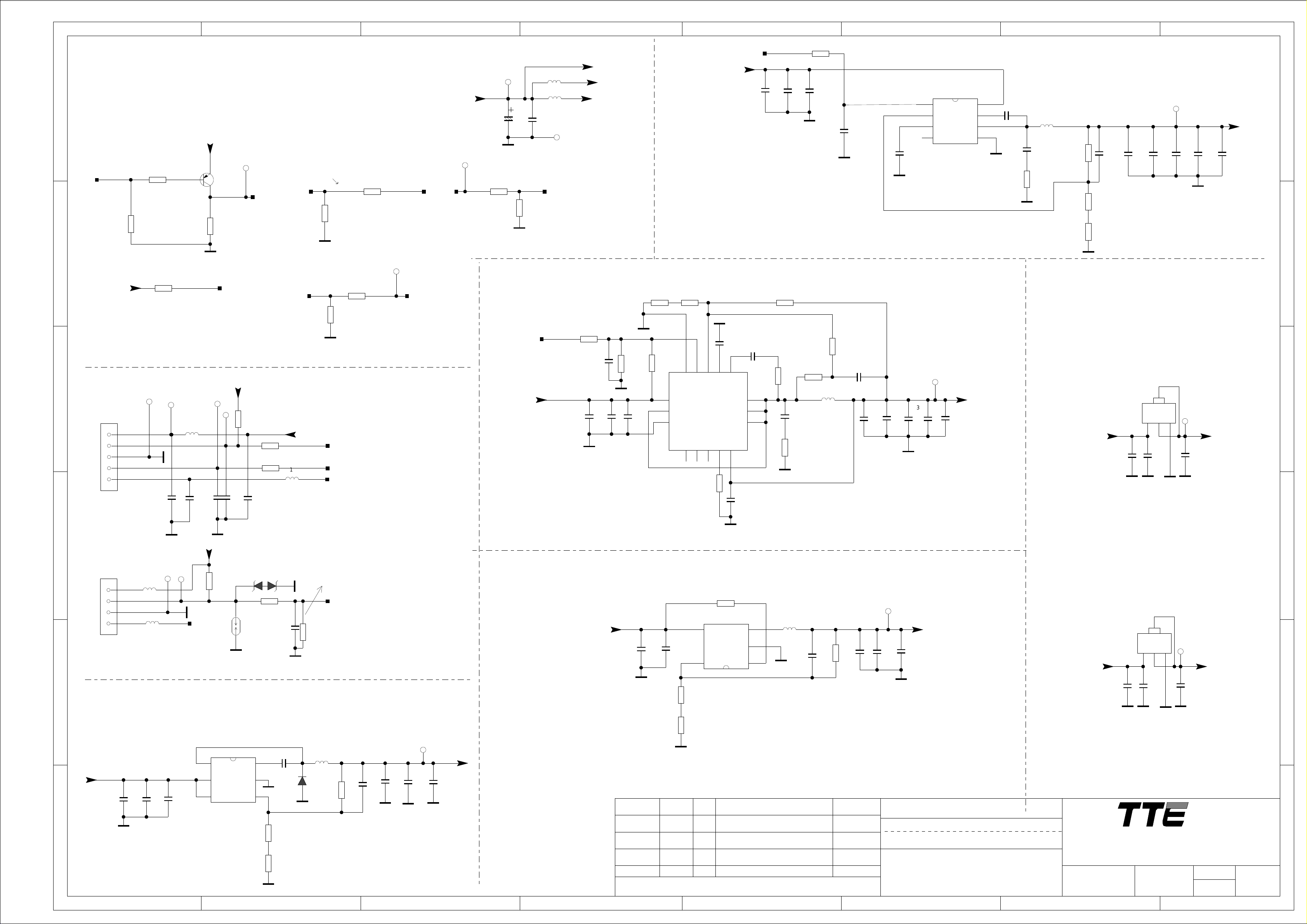
8 7 6 5
4 3 2 1
R001
POWER_ON
1K
C027
0.1U
C029
0.22U
(Vin=4.5V-18V)
C003
10U
R017
4R7
9
16
8
10U
GND
R015
100K
NC/
220P
R018
NC/
10R
GND
Fixed Fsw=500KHZ
Fixed OCP=6.7A
R019
1M
C005C004
0.1U
L005
1UH
GND
R020
510R
C006
0.1U
C030
220P
C032
22UC031
GND
C033
22U
C007
2U2
GND
C034
22U
U001 TPS56528
1
EN
2
VFB
3
VREG5
4
PG
Fsw=650KHz
VIN
VBST
SW
GND
8
7
6
5
GND
12V TO 1V2
CORE_1V2
T
max5A
CORE_1V2
C036
C035
22U
0.1U
0.1UC008
220P
C009
GND
MAIN POWER
12V
12V
L001
T
220R
L002
220R
12V
12V_AMP
12V_M
12V_M
F
C002
R208
220R
GND
C001
16V
470U
DIM_OUT
GND
12V_M
R209
10K
0.01U
(5)
POWER_ON
T
P_GND
C023
/NC
R010
3K3
C026
0.1U
(Vin=5V-22V)
C024
10U
10U
GND
GND
R011
47K
GND
C025
0.1U
R013
8K2
NC/
100K
15
1
2
R012
VIN
SW3
PGND
R014
91K
14
AGND
NC1
3
12
13
EN
U003
MP8765
PG
5
4
R016
NC/
0R
Vref=0.6V
GND
C028
1U
11
FB
VCC
NC2
MODE
6
10
BST
SW2
SW4
SW1
VOUT
7
MTK
3V3SB
L=>POWER_ON
H=>POWER_OFF
R201
10K
IR_GND
R200
10K
R203
T
10K
IR_3V3
IR
C900
0.01U
12_24_DETECT
T
L900
220R
GND
0.1U
C901
B
GND
LED_OUT
C902
220P
POWER_ON_OUT
(5)
E
3V3SB
D
1
2
3
4
5
P900
E
Q200
BT3906
C
POWER_ON
R202
10K
T
CA-0603
POWER_ON
3V3SB
IR
T
R900
10K
C903
470P
T
C904
0.1U
R901
470R
1K
R902
Must controlled by PWM
A_DIMING
(5)
R206
10K
BL_ON_OUT
(5)
3V3SB
IR_IN
LED_OUT
L901
600R
P
5V
GND
(5)
GND
R204
10K
R205
220R
R207
220R
ADIM
BL_ON
T
BL_ON
KEY Connector
(5)
(5)
PDIM
T
PDIM
12V TO 5V
L003
4.7UH
NC/
R002
6R8
NC/
R003
Vref=0.6V
R005
820R
33K
R004
3K6
GND
+5V
T
C010
22P
NC/
C011
10U10U
C013C012
10U
GND
C014
10U
LDO 5V TO 3V3
4
4
VIN
3
C038
0.1U
OUT
2
GND/ADJ
1
GND
3V3
T
C039
10U
GNDGND GND
U005
AS1117-3.3
C037
10U
3V35V
@max5A
C015
0.1U
F
5V
E
D
GND
GND
3V3SB
R903
47K
2 1
F900
GND
D900
PESD5V0S1BLNC/
R904
22K
C905
0.1U
NC/R905
GND
GND
Delete R114 when the I/O(KEY_IN) support 3.3V
*
KEY_IN
Without via on net KEY_IN
The distance between different net via>2mm
150K
(5)
C
GND
KEYKEY_GND
T
T
5V
P901
L902
600R
1
2
3
4
L903
600R
KEY
B
12V TO 3V3SB
SY8291,2015-04-23
GND
D050
SR34
L050
3.3UH
R050
300K
C054
1000P
C055
GND
6
LX
12V_M
(Vin=5V-40V)
GND
2.2U
C051C050
2.2U
C052
0.1U
5
IN
4
EN
AN_SY8291
FSW=800KHz
U002
A
BS
GND
FB
1
2
3
GND
GND
0.1U
0.6V
R051
30K
R052
36K
C053
THIS DRAWING CANNOT BE COMMUNICATED TO UNAUTHORIZED PERSONS COPIED UNLES S PERMITTED IN WRITING
22U
GND
3V3SB
C056
22U
T
GND
C057
0.1U
3V3SB
max:1.2A
5V
5
(Vin=2.5V-6V)
C040
10U
Index-Lab
C041
0.1U
GND
GND
...
...
...
...
DD-MM
DD-MM
DD-MM
DD-MM
DATE
Last saved :
Vref=0.6V
R023
33K
R024
33K
GND
C
DDR 1V5
R021
100K
U004
RT8096A
VIN
4
FB
5
...
...
...
...
LX
3
GND
2
EN
1
...
...
...
...
GND
L006
2.2UH
C042
22P
R022
100K
C043
22U
...
...
...
...
C044
22U
DDR_1V5
T
C045
0.1U
GND
SBU :
TCLNO:
.............
DDR_1V5
@max1A
DESIGNATION
DESCRIPTION Last modifNAME
5-5-2008_15:52
4678
...........
3 2 1
ON:
BY:
LDO 3V3 TO 1V8
4
4
U006
AS1117-1.8
3V3
C046
10U
TCL Thomson Electronics Ltd.
B Building, TCL Tower, Nanhai Road
Nanshan District, Shenzhen, Guangdong
Tel +86-755-3331xxxx Fax +86-755-3331xxxx
DRAWN
ON:
BY:
OUT
VIN
2
3
C047
0.1U
GND
CHECKED
DD-MM-YY
......
GND/ADJ
1
GNDGND GND
1V8
T
10U
1V8
C048
B
A
PAGE:
OF :
FORMAT DIN A2
Page 68

12 11 10 9 8 7 6 5 4 3 2 1
H
H
TUNER_FAT-
T
TUNER_FAT+
T
TU_3V3
TU_3V3
T
TUNER_SDA
T
TUNER_SCL
T
RF_SW
T
TU01
NC1
3V3
SCL
SDA
GND
NC2
NC3
IF_N
IF_P
IF_AGC
1
2
3
4
5
6
7
8
9
10
IF-AN
IF-AP
NC3
NC2
NC1
IF_AGC_D
VCC
SDA
SCL
GND
G
RF_SW
TUNER_FAT-
11
TUNER_FAT+
10
9
8
7
IF_AGC_T2
6
5
TUNER_SDA
4
TUNER_SCL
3
2
RF_SW
1
C939
0.02U
TU02
TU_3V3
10U
C245
TU_3V3
R134
4K7
Close to SOC
Or connect to the nearest 3V3
R135
4K7
TUNER_SCL
TUNER_SDA
(5)
(5)
G
C246
3V3
Close to Tuner
R988
F
RF_SW
R987
33R
R989
GND
Close to SOC
10K
R990
10K
33R
SW_RF
(5)
5V
U101
AS1117-3.3
C105
10U
GND
VIN
GND
3
C106
4
4
OUT
2
GND/ADJ
1
GND
TU_3V3
C107
10U0.1U
GND
T
C248
0.1U
TU_IFAGC
1K
R249
10P
C247
10P
IF_AGC_T2
Close to SOC
1K
R250
C249
0.1U
10K
R251
TU_3V3
IF_AGC
(5)
TUNER_FAT+
TUNER_FAT-
C148
22P
GND
R127
R128
C149
22P
100R
100R
GND
NC/
C150
22P
GND
NC/
C151
22P
Close to MTK SOC
R129
1K
R130
1K
GND
GND
NC/
C154
NC/
C155
R131
680R
22P
22P
C152
C153
0.1U
0.1U
(5)
IFP
SOC OPTION
(5)
IFN
F
E
Read Add:0X81H
Write Add:0X80H
C168
10P
GND
GND
L103
120R
C165
0.01U
C162
NC/
47P
GND
C166
1U
C163
NC/
C167
2U2
GND
47P
3V3_DEMO
3V3_DEMO
1V1
D_IF_AGC
R985
R986
4K7
4K7
GND
37
38
39
40
41
42
43
44
45
46
47
48
GND
SIFIP
SIFIN
SIFQP
SIFQN
RSSI
CLK_IO
TIFP
TIFN
VDD33D
CVDD5
GPO2
GPO3
4
4
VIN
3
C109
OUT
2
GND
R108
100K
GND/ADJ
DEMO_3V3
T
1
GND
VIN
4
FB
5
Vref=0.6V
C110
10U0.1U
U103
RT8096A
R107
100K
LX
GND
EN
3V3_DEMO
C112
C111
2U210U
GND
L101
2.2UH
3
2
1
C119
22P
GND
R110
100K
C120
22U
C121
22U
C113
0.1U
C122
0.1U
0.1U
GND
C115C114
0.1U
1V1
@max1A
C116
0.1U
IF_AGC_T2
Close tuner
R118
1K
Close demod
10K
R119
D_IF_AGC
U102
AS1117-3.3
5V
C108
GND
10U
C118
0.1U
GNDGND
D
5V
(Vin=2.7V-7)
C117
10U
3V3_DEMO
1V1
L104
120R
C164
2U2
TUNER_FAT+
TUNER_FAT-
24M
X100
35
32
34
33
CAVDD
ADDR
30
31
XTALO
XTALI
DISEQC_IN
36
GND1
AVDD33
U100
ATBM7812B
SDAM
SCLM
CVDD1
GPO5
GPO4
VDD33A
123456789
3V3_DEMO
1V1
GND
3V3_DEMO
28
29
261127
GP01
DISEQC_OUT
TEST_MODE
VDD33C
STATUS
TSSYNC
TSVLD
TSCLK
10
TSSYNC
TSCLK
TSVLD
C169
10P
1V1
25
GND
CVDD4
SDAS
SCLS
CVDD3
RESET
CVDD2
VDD33B
TS7
TS6
TS5
TS4
TS3
TS2
TS0
TS1
12
D_TSDATA1
D_TSDATA0
24
23
22
21
20
19
18
17
16
15
14
13
RT18/RT19/RT20 decided by the MTK SOC
3V3_DEMO
R151
47K
1V1
3V3_DEMO
D_TSDATA7
D_TSDATA6
D_TSDATA5
D_TSDATA4
D_TSDATA3
D_TSDATA2
R149
0R
R150
NC/
0R
1V1
GND
C171
10P
GND
GNDGND
C170
1U
T2_RST
R132 100R
R133 100R
C172
10P
(5)
TUNER_SDA
TUNER_SCL
(5)
(5)
E
D
GND
C134
0.1U
C
495mA
1V1
C123
22U
GND
GND
C124
10U
R109
15K
C125
2U2
C126
1V1
C128C127
0.1U0.1U
0.1U
C129
0.1U
GND
C135
0.1U
B
GND
R148
2K7
TSCLK
TSVLD
TSSYNC
R136
22R
R137
22R
R138
22R
C173
10P
C174
10P
/NC/NC
CI_MCLKI
CI_MIVAL
CI_MISTRT
C175
10P
GND
/NC
D_TSDATA7
D_TSDATA6
D_TSDATA5
D_TSDATA4
D_TSDATA3
D_TSDATA2
D_TSDATA1
D_TSDATA0
22RR139
R140 22R
22RR141
R142 22R
22R
R143
R144
22R
R145 22R
22RR146
C
CI_MDI7
CI_MDI6
CI_MDI5
CI_MDI4
CI_MDI3
CI_MDI2
CI_MDI1
CI_MDI0
A
THIS DRAWING CANNOT BE COMMUNICATED TO UNAUTHORIZED PERSONS COPIED UNLES S PERMITTED IN WRITING
...
...
...
...
Index-Lab
Last saved :
DD-MM
DD-MM
DD-MM
DD-MM
...
...
...
...
...
...
...
...
...
SBU :
TCLNO:
.............
TCL Thomson Electronics Ltd.
B Building, TCL Tower, Nanhai Road
A
Nanshan District, Shenzhen, Guangdong
...
...
NAME Last modifDESCRIPTIONDATE
5-5-2008_16:29
...
DESIGNATION
...........
ON:
BY:
DRAWN
Tel +86-755-3331xxxx Fax +86-755-3331xxxx
CHECKED
DD-MM-YY
ON:
BY:
......
PAGE:
OF :
123456789101112
FORMAT DIN A1
Page 69

8 7 6 5 4 3 2 1
MINI AV
AV_V
AV_GND
T
AV_V
T
Close to Connector
AV_L
T
AV_R
T
GND
AV_R
AV_L
F903
F902
VGA JACK
CVBS
GND
1
R
2
3
L
4
5
F901
F
P902
E
Close to Connector
AV_V
AV_L
AV_R
AV_V
D901
PESD5V0S1BL
2 1
R909
33K
R910
33K
R907
75R
NC/
150P
C911
C906
NC/
GND
47P
GND
NC/
150P
C912
CLOSE TO U001
R908
100R
C909 1U
1UC910
0.047UC907
1UC908
AV1_L_IN
AV1_R_IN
AV1_V_IN+
AV1_V_IN-
(5)
(5)
(5)
(5)
F
E
GND
D
D
AV AUDIO OUT
T
GND-AVOUT
1
GND
P903
3
R
L
2
4
D902
PESD5V0S1BL
C
PESD5V0S1BL
GND
B
D903
21
AVOUT1_R
AVOUT1_R
T
R911
470R
AR2_ADAC
C
AVOUT1_L
R912
21
T
AVOUT1_L
C913
C914
470P
GND
470R
470P
AL2_ADAC
B
SPDIF
A
THIS DRAWING CANNOT BE COMMUNICATED TO UNAUTHORIZED PERSONS COPIED UNLES S PERMITTED IN WRITING
SPDIF
T
2
1
T
SPDIF
NC/
F904
12
D904
PESD5V0S1BL
GND
R338
120R
P904
BLACK
SPDIF_GND
45678
R913
220R
C915
220P
Close to IC
C916 0.1U
SPDIF_OUT
A
123
FORMAT DIN A3
Page 70

12 11 10 9 8 7 6 5 4 3 2 1
USB2.0 Port
H
H
D905
D906
D907
D908
NC/
NC/
NC/
NC/
GND
INTERNET
Must be differential 100ohm
2R2
TXVP
TXVN TXN
RXVP
RXVN
R923
R924
13-ESD3V3-6PB
R925 2R2
2R2
R926
2R2
D909
RXP
RXN
TXP
4
7
65
312
• WIFI
USB3D+
USB3D-
C930
3P3
NC/
GND
WIFI_SW
T
C931
0.01U
GND
T T
D910
1
GND
9108
2
3
4
NC/
ESD
13-ESD5V5-O4B0P5
10
9
8
GND
7
65
C925
0.1U
C926
0.1U
C924
0.01U
GND GND
C927
0.01U
U901
1
2
3
4
5
6
7
TS8121CLF
P907
GND
11
12
1
2
3
4
5
6
7
8
9
10
USB3_DM
USB3_DP
WIFI_ON
R933 100R
5V
R931 2R2
R932 2R2
C929
3P3
NC/
16
TX1P
15
TX1N
14
13
12
RX1P
11
10
RX1N
98
R927
75R
R928
75R
GND
C928
1000P
R929
75R
R930
75R
TXC
RXC
TP
TN
RP
TC
RN
RC
T
T
T TT T
GND
TX1P
TX1N
RX1P
TXC
RX1N
RXC
C932
0.1U
WGND
WIFI_PWR
T
GND
GND
T
1
2
3
4
5
6
P908
R934 0R
G
F
U900
RT9711A
5V
C917
10U
GND
USB2_DM
(5)
USB2_DP
(5)
G
3V3SB
R917
4K7
F
5 1
VIN
R914
10K
4
EN/EN# NC
R915 2R2
R916 2R2
R918
4K7
UART_TX
UART_RX
C918
3P3
VOUT
GND
C919
NC/
(5)
(5)
3P3
2
3
GND
C920
470U
NC/
16V
USB1_DM
USB1_DP
USB_5V
C921
10U
GND
R919
R920 2R2
USB_5V
C922
USB1_D-
T
T
USB1_D+
F906
F905
GND
USB_5V
2R2
3P3
NC/
NC/
GND
T
C923
3P3
GND
T
GND
GND
GNDU
P905
1
U2_DM
U2_DP
VCC-1
2
DNEG-1
3
DPOS-1
4
GND-1
5
6
MNT-HOLE1
MNT-HOLE2
When use ESD Device, must delete 3.3pF on USB data line
UART_RX
T
0.1U
C419
U1_DM
USB2_D-
T T
USB2_D+
T
GND
F908F907
UART_TXUSB_5V
T T
UART_RX
UART_TX
U1_DP
R921
NC/470R
R922
NC/470R
GND
9
1
8
2
7
3
6
4
5
10
11
U1_DP
U2_DP
U1_DM
U2_DM
P906
MNT-HOLE1
MNT-HOLE2
2 1
PESD5V0S1BL
2 1
PESD5V0S1BL
2 1
PESD5V0S1BL
2 1
PESD5V0S1BL
HDMI/MHL Prot1
HDMI Port2
E
3
R943
10K
MHL_SENSE
12
H1_HPD
R948
20K
5V
H1_SCL
H1_SDA
H1_SCL
H1_SDA
VBUS
B
C
E
GND
B
Q900
BT3904
GND
VBUS
D911
BAT54C
1 2
R942
4K7
D
H1_SCL_IN
(5)
H1_SDA_IN
(5)
R417
100R
R418
100R
D914
2 1
PESD5V0S1BL
D915
2 1
PESD5V0S1BL
D916
C
PESD5V0S1BL
D917
2 1
PESD5V0S1BL
D918
2 1
PESD5V0S1BL
GND
MHL_SENSE
B
3V3SB
3V3SB
R946
300K
R947
47K
C
E
(5)
(5)
(5)
(5)
(5)
(5)
(5)
Q901
BT3904
H1_RX2+
MHL_SENSE
H1_RX2-
H1_RX1+
H1_RX1MHL+/H1_RX0+
MHL-/H1_RX0-
H1_CLK+
(5)
H1_CLK-
(5)
R949
10K
S
G
D
3
1
100R
4R7
4R7
4R7
4R7
4R7
4R7
VBUS
Q904
PMV65XP
BAT54A
2
R950
820R
R951
33R
4R7
4R7
D919
H1_RX2+_IN
R935
R936
H1_RX2-_IN
R937
R938
R939
MHL+/H1_RX0+_IN
R940
MHL-/H1_RX0-_IN
R941
H1_CLK+_IN
R944
H1_CLK-_IN
R945
MHL_PWR_EN
H1_HPD
H1_RX1+_IN
H1_RX1-_IN
5V
GND
R952
100R
1
2
GND
3
4
D912
1
2
3
4
D913
13-ESD5V5-O4B0P5
C933
0.1U
GND
R953
300K
ESD
13-ESD5V5-O4B0P5
10
9
8
7
65
ESD
VBUS
H1_HPD
C934
10U
4 3
EN/EN# OC
G524
C935
0.047U
GND
10
9
8
7
65
H_CEC
GND
U902
OUTIN
GND
GND
H1_SCL
H1_SDA
15
2
GND
1
2
3
4
5
6
7
8
9
10
11
12
13
14
15
16
17
18
19
0.1U
P909
GND1
RX1+
RX1-
GND3
RXC+
RXC-
NC2
DDCDA
VCC
C937C936
10U
GND
RX2+
RX2-
GND2
RX0+
RX0-
GND4
NC1
DDCCLK
GND5
HPD
VBUS
RX2+
GND1
RX2-
GND2
RX0+
RX0-
GND4
NC1
DDCCLK
GND5
HPD
3V3SB
3V3SB
P910
RX1+
RX1-
GND3
RXC+
RXC-
NC2
DDCDA
VCC
R966
47K
H2_RX2+_IN
H2_RX2-_IN
ESD
R970
100K
10
9
8
7
65
R962
R963
H2_HPD
10
9
8
7
65
100R
100R
GND
H2_SCL_IN
H2_SDA_IN
GND
H2_RX1+_IN
H2_RX1-_IN
H2_RX0+_IN
H2_RX0-_IN
H2_RXC+_IN
H2_RXC-_IN
(5)
(5)
1
2
GND
3
4
ESD
D920
13-ESD5V5-O4B0P5
1
2
3
4
5
6
7
8
9
10
11
12
B
H_CEC
H1_ARC
H2_SCL
H2_SDA
H2_5V
H2_HPD
(5)
C
BT3904
E
GND
R967
47K
HDMI2_HPD
Q902
R968
910R
13
14
15
16
17
18
19
GND
GND
B
1
2
3
4
D921
13-ESD5V5-O4B0P5
R964
47K
47KR965
H2_5V
R969
75R
C
Q903
BT3904
E
GND
4R7
4R7
4R7
4R7
4R7
4R7
4R7
4R7
GND
H2_RX2+
R954
H2_RX2-
R955
H2_RX1+
R956
H2_RX1-
R957
H2_RX0+
R958
H2_RX0-
R959
H2_CLK+
R960
H2_CLK-
R961
D922
2 1
PESD5V0S1BL
D923
PESD5V0S1BL
D924
2 1
PESD5V0S1BL
D925
2 1
PESD5V0S1BL
12
H2_5V
(5)
(5)
(5)
(5)
(5)
(5)
(5)
(5)
H2_SCL
H2_SDA
H2_HPD
H_CEC
27K
R983
3V3SB
D930
R984
100R
HDMI_CEC
27K
R979
82R
R980
GND
5V
47K
R981
1UC938
R982
H1_ARCH1_ARC_OUT
47K
GND
When AC power OFF and HDMI sourc is plugged in, HPD is Low
H1_HPD_CBUS
GND
When Power on or Standby and HDMI source is plugged in, HPD is High
For MTK5507, reading EDID when HPD is High
E
D
C
A
THIS DRAWING CANNOT BE COMMUNICATED TO UNAUTHORIZED PERSONS COPIED UNLES S PERMITTED IN WRITING
...
...
...
...
Index-Lab
Last saved :
DD-MM
DD-MM
DD-MM
DD-MM
...
...
...
...
...
...
SBU :
TCLNO:
TCL
ADDRESS1
...
...
...
.............
ADDRESS2
A
ADDRESS3
...
...
NAME Last modifDESCRIPTIONDATE
11-23-2010_14:02
...
DESIGNATION
...........
TELEPHONE
DRAWN
ON:
BY:
CHECKED
DD-MM-YY
ON:
BY:
......
PAGE:
OF :
123456789101112
FORMAT DIN A1
Page 71

12 11 10 9 8 7 6 5 4 3 2 1
H
H
SOC-POWER
CORE_1V2
U201MT5507
Y16
VCCK
W17
VCCK1
Y17
VCCK2
W18
VCCK3
Y18
VCCK4
P19
VCCK5
R19
VCCK6
T19
VCCK7
U19
VCCK8
V19
VCCK9
W19
VCCK10
Y19
VCCK11
P20
VCCK12
R20
VCCK13
T20
VCCK14
U20
VCCK15
V20
VCCK16
W20
VCCK17
G
Y20
U21
V21
W21
VCCK18
VCCK19
VCCK20
VCCK21
VCCK22
VCCK23
VCCK24
VCCK25
VCCK26
VCCK27
VCCK28
VCCK29
VCCK30
VCCK31
VCC3IO_A
VCC3IO_B
F
Y21
W22
Y22
AA22
AB22
Y23
AA23
AB23
AA24
AB24
G21
F22
C200
0.1U
CORE_1V2
C201
NC/
0.1U
GND
C202
4U7
3V3
(3)
(3)
3V3
GND
C216
1U
AV1_R_IN
AV1_L_IN
C217
0.1U
SOC-AUDIO
C22
AIN_R0
C24
AIN_L0
B23
AIN_R1
E23
AIN_L1
D23
AIN_R2
A22
AIN_L2
B22
AIN_R3
C23
AIN_L3
AVDD33_ADAC
E21
AVDD33_AADC
D22
VMID_AADC
K19
AVSS33_CLN
GND
U201MT5507
AR0_ADAC
AL0_ADAC
AR1_ADAC
AL1_ADAC
AR2_ADAC
AL2_ADAC
ASPDIFI
ASPDIFO0
AOBCK
AOLRCK
AOMCLK
AOSDATA1
AOSDATA0
A25
C25
B26
A27
B25
A26
F21
AG27
AH28
AF27
AD26
AG28
AE27
AF28
AR2_ADAC
AL2_ADAC
C219 10U
GND
H1_ARC_O
SPDIF_OUT
I2S_BCLK
I2S_LRCK
I2S_MCLK
I2S_DATA
SOC-VEDIO
HDMI_CEC
(4)
U201MT5507
(2)
(2)
IFP
IFN
CORE_1V2
C220 0.1U
(3)
(3)
3V3
(2)
GND
IF_AGC
0.1UC218
TUNER_SCL
(2)
TUNER_SDA
(2)
(5)
(8)
(8)
(8)
(3)
(3)
(3)
AV1_V_IN-
AV1_V_IN+
(8)
D27
ADCINP_DEMOD
D28
ADCINN_DEMOD
E27
AVDD12_DEMOD
F15
IF_AGC
E14
RF_AGC
E15
OSCL1
D15
OSDA1
H27
CVBS_COM
H28
CVBS3P
J25
CVBS2P
G28
CVBS1P
G26
CVBS0P
G25
SIF_COM
HSYNC
VSYNC
RP
GP
BP
COM
SOG
VGA_SDA
VGA_SCL
COM1
PB1P
PR1P
Y1P
SOY1
COM0
PB0P
PR0P
Y0P
SOY0
VDACX_OUT
AVDD33_VIDEO_STB
AVSS33_XTAL
AVSS33_DEMOD
R27
R28
N26
N28
P28
N27
P27
T28
T27
M25
L28
L27
M26
N25
K26
K25
J26
K27
K28
G27
H23
J20
K20
AVOUT_V
3V3SB
C221 0.1U
GND
75R
GND
AVOUT_V
T
R210
CORE_1V2
CORE_1V2
GND
(4)
(4)
(4)
(4)
(4)
(4)
H1_HPD_CBUS
(4)
HDMI2_HPD
(4)
HDMI3_HPD
(4)
(4)
GND GND
AVDD33_HDMI
H1_SCL_IN
H2_SCL_IN
H3_SCL_IN
H1_SDA_IN
H2_SDA_IN
H3_SDA_IN
MHL_SENSE
C222 0.1U
3V3
5V
0.1UC223
SOC-HDMI
MT5507
C19
HDMI_CEC
C16
HDMI_0_SCL
D19
HDMI_1_SCL
U23
HDMI_2_SCL
D16
HDMI_0_SDA
G19
HDMI_1_SDA
U24
HDMI_2_SDA
E18
HDMI_0_PWR5V
E17
HDMI_0_HPD_CBUS
F19
HDMI_1_HPD
T22
HDMI_2_HPD
E16
MHL_SENSE
A14
AVDD12_HDMI
U26
AVDD12_HDMI1
G20
AVDD33_HDMI
Q201
RTR040N03
HDMI_0_RX_0
HDMI_0_RX_0B
HDMI_0_RX_1
HDMI_0_RX_1B
HDMI_0_RX_2
HDMI_0_RX_2B
HDMI_0_RX_C
HDMI_0_RX_CB
HDMI_1_RX_0
HDMI_1_RX_0B
HDMI_1_RX_1
HDMI_1_RX_1B
HDMI_1_RX_2
HDMI_1_RX_2B
HDMI_1_RX_C
HDMI_1_RX_CB
HDMI_2_RX_0
HDMI_2_RX_0B
HDMI_2_RX_1
HDMI_2_RX_1B
HDMI_2_RX_2
HDMI_2_RX_2B
HDMI_2_RX_C
HDMI_2_RX_CB
U201
A17
B17
A16
B16
A15
B15
C17
D17
A20
B20
A19
B19
C18
D18
C21
B21
W26
W25
V26
V25
V28
V27
Y28
Y27
MHL+/H1_RX0+
MHL-/H1_RX0-
H1_RX1+
H1_RX1-
H1_RX2+
H1_RX2-
H1_CLK+
H1_CLK-
H2_RX0+
H2_RX0-
H2_RX1+
H2_RX1-
H2_RX2+
H2_RX2-
H2_CLK+
H2_CLK-
H3_RX0+
H3_RX0-
H3_RX1+
H3_RX1-
H3_RX2+
H3_RX2-
H3_CLK+
H3_CLK-
(4)
(4)
(4)
(4)
(4)
(4)
(4)
(4)
(4)
(4)
(4)
(4)
(4)
(4)
(4)
(4)
(4)
(4)
(4)
(4)
(4)
(4)
(4)
(4)
When input is 12V reset vol:8.4V
R212
3K9
GND
AVDD33_HDMI
SOC RESET
MTK
Reset at low level
When input is 12V,reset time is 80ms
12V_M
R217
0R
C225
1U
GND
R213
33K
R214
100K
R215
8K2
Q202
E
BT3906
R216
47K
MCU_RESET
T
C226
0.1U
B
C
R218
3K3
NC/
Q203
BT3906
3V3SB
E
C
C227
0.01U
R219
470R
B
MCU_RESET
R220
10K
R221
10K
G
RESET_CON
F
GND
CORE_1V2
C203
22U
C204
10U
C205
4U7
Bottom SIDE
C207
C206
0.1U
10U
C208
0.1U
C209
0R
H1_ARC_O
(5)
C214
0.1U
C215
0.1U
C213
C212
C211C210
0.1U
0.1U
0.1U
0.1U0.1U
R978
H1_ARC_OUT
(4)
R211
1K
R252
100K
GND
GND
C224
0.1U
GND
GND
E
E
SOC-EMMC
SYS_SCL
SYS_SDA
MT5507
AB1
DVSS
AG1
DVSS1
L2
DVSS2
AC2
DVSS3
H3
DVSS4
J3
DVSS5
N3
D
C
DVSS6
R3
DVSS7
V3
DVSS8
Y3
DVSS9
M4
DVSS10
AD4
DVSS11
AF4
DVSS12
J5
DVSS13
P5
DVSS14
AB5
DVSS15
E6
DVSS16
F6
DVSS17
G6
DVSS18
K6
DVSS19
AH6
DVSS20
E7
DVSS21
F7
DVSS22
G7
DVSS23
H7
DVSS24
U7
DVSS25
W7
DVSS26
AF7
DVSS27
E8
DVSS28
F8
DVSS29
G8
DVSS30
H8
DVSS31
U8
DVSS32
AA8
DVSS33
E9
DVSS34
F9
DVSS35
G9
DVSS36
K9
DVSS37
L9
DVSS38
M9
DVSS39
N9
DVSS40
AB9
DVSS41
AH9
DVSS42
K10
DVSS95
L10
DVSS96
M10
DVSS116
N10
DVSS110
AF10
DVSS118
K11
DVSS109
L11
DVSS119
M11
DVSS102
N11
DVSS103
P11 N16
DVSS99 DVSS100
R11
DVSS98
T11
DVSS115
U11
DVSS107
V11
DVSS108
W11
DVSS101
C12
DVSS117
C15
DVSS166
U201
DVSS43
DVSS44
DVSS45
DVSS46
DVSS47
DVSS48
DVSS49
DVSS50
DVSS51
DVSS52
DVSS53
DVSS54
DVSS55
DVSS56
DVSS57
DVSS58
DVSS59
DVSS60
DVSS61
DVSS62
DVSS63
DVSS64
DVSS65
DVSS66
DVSS67
DVSS68
DVSS69
DVSS70
DVSS71
DVSS72
DVSS73
DVSS74
DVSS75
DVSS76
DVSS77
DVSS78
DVSS79
DVSS80
DVSS81
DVSS82
DVSS83
DVSS84
DVSS85
DVSS86
DVSS87
DVSS88
DVSS89
DVSS90
DVSS91
DVSS92
DVSS93
DVSS94
DVSS106
DVSS104
DVSS113
DVSS105
DVSS114
DVSS111DVSS112
DVSS97
K12
L12
M12
N12
P12
R12
T12
U12
V12
W12
K13
L13
M13
N13
P13
R13
T13
U13
V13
W13
AB13
AC13
AD13
AF13
G14
J14
K14
L14
M14
N14
P14
R14
T14
U14
V14
W14
AD14
AE14
J15
K15
L15
M15
N15
P15
R15
T15
U15
V15
J16
K16
L16
M16
P16
R16
T16
U16
V16
W16AB11
AB16
3V3SB
1V8
GND
(9)
(9)
10UC228
C229 0.1U
3V3SB
C230
1U
GND
B
J17
K17
L17
M17
N17
P17
R17
T17
U17
V17
J18
K18
L18
DVSS126
DVSS124
DVSS127
DVSS121
DVSS130
DVSS132
DVSS129
DVSS128
DVSS120
DVSS125
DVSS122
DVSS123
DVSS131
DVSS137
DVSS140
DVSS144
DVSS138
DVSS134
DVSS141
DVSS133
DVSS142
DVSS136
DVSS139
DVSS143
DVSS145
DVSS135
M18
N18
P18
R18
T18
U18
V18
AB18
L19
M19
N19
AB19
L20
(8)
(8)
C231
0.1U
(7)
(7)
GND
R224
R225
3V3SB
4K7
3V3
4K7
MT5507
SYS_SDA
SYS_SCL
XTAL_I
XTAL_O
GND
C232 0.1U
GND
C233
4U7
C234
4U7
AE26
OSDA0
AH26
OSCL0
B28
XTALI
B27
XTALO
J22
AVDD33_REG_STB
J1
VCC3IO_EMMC
H24
AVDD33_RGB_STB
K21
AVSS33_RGB
J23
AVDD33_PLL_STB
U25
AVDD10_LDO
Y26
AVDD10_ELDO
GND
Crystal oscillator port
XTAL_I
XTAL_O
R222
0R
R223
NC/
1M
C250
X200
24M
C251
33P
33P
EMMC_CLK
EMMC_RST
FSRC_WR
GNDGND
U201
U0TX
U0RX
POWE#
POOE#
POCE1#
POCE0#
PDD7
PDD6
PDD5
PDD4
PDD3
PDD2
PDD1
PDD0
PARB#
PACLE
PAALE
OPWRSB
ORESET#
OIRI
T25
T24
EMMC_CMD
J2
N7
M7
L7
EMMC_D7
P3
EMMC_D6
N1
EMMC_D5
N2
EMMC_D4
N4
EMMC_D3
M3
EMMC_D2
L1
N6
P6
N5
EMMC_D1
L3
EMMC_D0
K3
EMMC_CLK
P4
EMMC_RST
P7
POWER_ON_OUT
R26
MCU_RESET
L25
L26
AH27
UART_TX
UART_RX
SPI_CSN
SPI_SDI
SPI_SDO
IR_IN
R226
4K7
(7)
(7)
(7)
(7)
(7)
(7)
(7)
(7)
(7)
(7)
(7)
GND
(1)
(4)
(4)
CI_MCLKI
CI_MIVAL
CI_MISTRT
CI_MDI1
CI_MDI2
CI_MDI3
CI_MDI4
CI_MDI5
CI_MDI6
CI_MDI7
R260
47R
R261
47R
R262
47R
R263
47R
R264
47R
R265
47R
R266
47R
R267
47R
R268
47R
R269
47R
R270
47R
Close to Main Chip
(1)
(7)
(1)
(9)
(8)
(1)
(4)
CI_A0
CI_A1
CI_A2
CI_A3
CI_A4
CI_A5
CI_A6
CI_A7
CI_A8
CI_A9
CI_A10
CI_A11
CI_A12
CI_A13
CI_A14
CI_MCLKI_S
CI_MIVAL_S
CI_MISTRT_S
CI_MDI0_SCI_MDI0
CI_MDI1_S
CI_MDI2_S
CI_MDI3_S
CI_MDI4_S
CI_MDI5_S
CI_MDI6_S
CI_MDI7_S
CI_D0
CI_D1
CI_D2
CI_D3
CI_D4
CI_D5
CI_D6
CI_D7
CI_MDO0
CI_MDO1
CI_MDO2
CI_MDO3
CI_MDO4
CI_MDO5
CI_MDO6
CI_MDO7
12_24_DETECT
RESET_CON
OPCTRL3
E_WP
3D_CTR
PANEL_ON/OFF
AMP_RESET
BL_ON_OUT
MHL_PWR_EN
strapping
SOC-CI
D2
CI_A0
D1
CI_A1
C3
CI_A2
C1
CI_A3
C2
CI_A4
B1
CI_A5
A1
CI_A6
A2
CI_A7
C5
CI_A8
B5
CI_A9
D6
CI_A10
A5
CI_A11
A3
CI_A12
D5
CI_A13
E4
CI_A14
B4
CI_MCLKI
H5
CI_MIVAL
D4
CI_MISTRT
D3
CI_MDI0
E5
CI_MDI1
F5
CI_MDI2
H6
CI_MDI3
H4
CI_MDI4
A4
CI_MDI5
B3
CI_MDI6
C4
CI_MDI7
E1
CI_D0
E2
CI_D1
G3
CI_D2
D9
CI_D3
B9
CI_D4
B8
CI_D5
B7
CI_D6
D7
CI_D7
E3
CI_MDO0
F3
CI_MDO1
G2
CI_MDO2
A9
CI_MDO3
A8
CI_MDO4
A7
CI_MDO5
C7
CI_MDO6
C6
CI_MDO7
P26
OPCTRL0
P25
OPCTRL1
P24
OPCTRL2
N24
OPCTRL3
M24
OPCTRL4
M23
OPCTRL5
M22
OPCTRL6
K23
OPCTRL7
L23
OPCTRL8
E20
OPCTRL9
D20
OPCTRL10
G18
OPCTRL11
F18
OPCTRL12
GPIO0
GPIO1
GPIO2
GPIO3
GPIO4
GPIO5
GPIO6
GPIO7
GPIO8
GPIO9
GPIO10
GPIO11
GPIO12
GPIO13
GPIO14
GPIO15
GPIO16
GPIO17
GPIO18
GPIO19
GPIO20
GPIO21
GPIO22
GPIO23
GPIO24
GPIO25
GPIO26
GPIO27
GPIO28
GPIO29
GPIO30
GPIO31
GPIO32
GPIO33
GPIO34
GPIO35
GPIO36
GPIO37
GPIO38
GPIO39
GPIO40
GPIO41
U201MT5507
DEMOD_RST
DEMOD_TSCLK
DEMOD_TSDATA0
DEMOD_TSSYNC
DEMOD_TSVAL
CI_INT
CI_TSCLK
CI_TSDATA0
CI_TSSYNC
CI_TSVAL
CI_RST
PVR_TSCLK
PVR_TSVAL
PVR_TSSYNC
PVR_TSDATA0
PVR_TSDATA1
SPI_CLK1
SPI_CLK
SPI_DATA
SPI_CLE
OPWM2
OPWM1
OPWM0
SD_D0
SD_D1
SD_D2
SD_D3
SD_CMD
SD_CLK
VCC3IO_SD
LED_PWM0
LED_PWM1
GPIO42
GPIO43
GPIO44
GPIO45
GPIO46
GPIO47
ADIN0_SRV
ADIN1_SRV
ADIN2_SRV
ADIN3_SRV
ADIN4_SRV
ADIN5_SRV
ADIN6_SRV
ADIN7_SRV
E13
F13
F12
F11
G13
D10
D12
E11
F4
E12
B2
E10
A11
F10
B11
C9
G1
C11
D11
C10
AE25
AG26
AF26
K4
L5
L4
L6
K5
H1
H2
R22
R24
J6
J7
G11
H11
H12
G12
K24
L24
J24
E28
F25
F26
H25
H26
LED_OUT
LED_PWM1
KEY_IN
T2_RST
CI_INT
CI_TSCLK
CI_TSDATA0
CI_TSSYNC
CI_TSVAL
CI_RST
PVR_TSCLK
PVR_TSVAL
PVR_TSSYNC
PVR_TSDATA0
PVR_TSDATA1
SPI_CLK1
SPI_CLK
SPI_DATA
SPI_CLE
A_DIMING
DIM_OUT
C252 0.1U
strapping
strapping
WIFI_ON
SW_RF
R239
10K
R238
10K
3V3
(2)
(1)
(1)
(4)
(2)
GND
(1)
GND
GND
(4)
(4)
(4)
(4)
(4)
(4)
3V3
USB1_DP
USB1_DM
USB2_DP
USB2_DM
USB3_DP
USB3_DM
SOC-USB
MT5507
B12
USB_DP_P0
A12
USB_DM_P0
C13
USB_DP_P1
D13
USB_DM_P1
D14
USB_DP_P2
C14
USB_DM_P2
AD28
USB_DP_P3
AD27
USB_DM_P3
F23
AVDD33_USB
C253
1U
GND
U201
STRAPPING
ICE mode + 24M + serial boot
ICE moce + 24M + ROM to 60bit ECC Nand boot
ICE moce + 24M + ROM to eMMC boot from
eMMC pins(share pins w/s NAND)
SOC-Ethernet
U201MT5507
3V3
3V3SB
TXVP_0
TXVN_0
RXVP_1
RXVN_1
PHYLED1
PHYLED0
REXT
AVDD33_ETH
NC/
AB27
AB26
AC25
AC26
AA25
AA26
AB28
AB25
R241
0R
0R
R242
TXVP
TXVN
RXVP
RXVN
R240
24K
AVDD33_ETH
AVDD33_ETH
C254
0.1U
GND
SOC Config
R553
10K
LED_OUT
R555
10K
LED_PWM1
R557
10K
OPCTRL3
LED_OUT
0 0
0
0
GND
LED_PWM0
D
GND
C
OPCTRL3
1
1
0
0
0
M20
N20
AB20
E22
P22
AC22
T23
AC23
AC24
D24
DVSS150
DVSS147
DVSS152
DVSS146
DVSS153
DVSS149
DVSS151
DVSS154
DVSS155
DVSS148
DVSS159
DVSS163
DVSS156
DVSS157
DVSS165
DVSS161
DVSS158
DVSS164
DVSS162
DVSS160
A
Y25
AD25
AF25
C26
D26
E26
T26
C27
A28
C28
GNDGND
THIS DRAWING CANNOT BE COMMUNICATED TO UNAUTHORIZED PERSONS COPIED UNLES S PERMITTED IN WRITING
...
...
...
...
Index-Lab
Last saved :
DD-MM
DD-MM
DD-MM
DD-MM
...
...
...
...
...
...
...
...
...
SBU :
TCLNO:
.............
TCL Thomson Electronics Ltd.
B Building, TCL Tower, Nanhai Road
A
Nanshan District, Shenzhen, Guangdong
...
...
NAME Last modifDESCRIPTIONDATE
5-5-2008_16:29
...
DESIGNATION
...........
ON:
BY:
DRAWN
Tel +86-755-3331xxxx Fax +86-755-3331xxxx
CHECKED
DD-MM-YY
ON:
BY:
......
PAGE:
OF :
123456789101112
FORMAT DIN A1
Page 72

8 7 6 5
4 3 2 1
DDR_1V5
SOC-DDR
F
RA0
RA1
RA2
RA3
RA4
RA5
RA6
RA7
RA8
RA9
RA10
RA11
RA12
RA13
RA14
RA15
RBA0
RBA1
RBA2
RCS
RCSD
RRAS
RCAS
E
R230
120R
48R7
R231
RWE
RODT
RCKE
RRESET
MCLK0
MCLK0B
DDRVREF_A1
DDRVREF_A2
ARTP
ARTN
GND
DDR_1V5
D
AB4
AC9
AE3
AE6
AD9
AE4
AC11
AD5
AE9
AE5
AE7
AD11
AE12
AC5
AE10
AE11
AD7
AE8
AC7
W4
AA5
AA6
AC4
W5
W6
AA4
AE13
W9
W8
AC20
AD20
AB12
V4
U6
Y4
U5
Y8
Y9
R4
T4
R5
T5
R6
T6
R7
T7
R8
V8
R9
T9
U9
V9
T8
MT5507
RA0
RA1
RA2
RA3
RA4
RA5
RA6
RA7
RA8
RA9
RA10
RA11
RA12
RA13
RA14
RA15
RBA0
RBA1
RBA2
RCS#
RCSD#
RRAS#
RCAS#
RWE#
RODT
RCKE
RRESET
RCLK0
RCLK0#
DDRVREF_A1
DDRVREF_A2
ARTP
ARTN
MEMTP
MEMTN
TP_HPCPLL
TN_HPCPLL
DDRV
DDRV1
DDRV2
DDRV3
DDRV4
DDRV5
DDRV6
DDRV7
DDRV8
DDRV9
DDRV10
DDRV11
DDRV12
DDRV13
DDRV14
DDRVA
U201
RDQM0
RDQS0
RDQS0#
RDQ0
RDQ1
RDQ2
RDQ3
RDQ4
RDQ5
RDQ6
RDQ7
RDQM1
RDQS1
RDQS1#
RDQ8
RDQ9
RDQ10
RDQ11
RDQ12
RDQ13
RDQ14
RDQ15
RDQM2
RDQS2
RDQS2#
RDQ16
RDQ17
RDQ18
RDQ19
RDQ20
RDQ21
RDQ22
RDQ23
RDQM3
RDQS3
RDQS3#
RDQ24
RDQ25
RDQ26
RDQ27
RDQ28
RDQ29
RDQ30
RDQ31
AVDD33_DDR
AVDD12_DDR
AVSS12_DDR
AA3
Y2
Y1
U3
AE2
T3
AE1
R2
AF2
R1
AF1
W2
AB3
AB2
AD2
U1
AD3
U2
AC3
V1
AC1
V2
AF8
AG7
AH7
AG3
AG12
AF3
AH12
AG2
AG13
AH2
AH13
AG6
AF9
AG9
AF12
AH4
AF11
AG4
AG10
AF5
AH10
AF6
U4
Y15
W15
RDQM0
RDQS0
RDQS0B
RDQ0
RDQ1
RDQ2
RDQ3
RDQ4
RDQ5
RDQ6
RDQ7
RDQM1
RDQS1
RDQS1B
RDQ8
RDQ9
RDQ10
RDQ11
RDQ12
RDQ13
RDQ14
RDQ15
RDQM2
RDQS2
RDQS2B
RDQ16
RDQ17
RDQ18
RDQ19
RDQ20
RDQ21
RDQ22
RDQ23
RDQM3
RDQS3
RDQS3B
RDQ24
RDQ25
RDQ26
RDQ27
RDQ28
RDQ29
RDQ30
RDQ31
C238 1U
GND
C239
0.1U
GND
3V3
CORE_1V2
1_A0
1_A1
1_A2
1_A3
1_A4
1_A5
1_A6
1_A7
1_A8
1_A9
1_A10
1_A11
1_A12
1_BA0
1_BA1
1_BA2
1_RCS
1_RAS#
1_CAS#
1_WE#
RODT
A_VREFCA1
1_A15
1_A13
1_A14
DDR_1V5
N3
A0
P7
A1
P3
A2
N2
A3
P8
A4
P2
A5
R8
A6
R2
A7
T8
A8
R3
A9
L7
A10
R7
A11
N7
A12
M2
N8
BA1
M3
BA2
L2
/CS
J3
/RAS
K3
/CAS
L3
/WE
K1
ODT
M8
VREFCA
J1
NC1
J9
NC2
L1
NC3
L9
NC4
M7
NC5
T3
NC6
T7
NC7
TOP SIDE
R310
240R
R9
VDD8
ZQ
L8
K2
K8
N1
N9
R1
VDD4
VDD5
VDD6
VDD7
H5TQ4G63CFR-RDC
VSS8
VSS9
VSS10
T1
P1
P9
GND
G7
VDD2
VDD3
VSS6
VSS7
M9
B2
D9
VDD1
U301
VSS5
J8
M1
VDD
VSS2
VSS3
VSS4
J2
E1T9B3
G8
Bottom SIDE
VSS1
A9
VSS
H2
H9
VDDQ8
VSSQ8
VSS11
G1
G9
E9
F1
VDDQ6
VDDQ7
VSSQ6
VSSQ7
F9
E8
C9
D2
VDDQ4
VDDQ5
VSSQ4
VSSQ5
E2
D8
A1A8C1
VDDQ2
VDDQ3
VSSQ2
VSSQ3
B9
D1
VDDQ
VDDQ1
VREFDQ
/RESET
VSSQ
VSSQ1
B1
DMU
DQSU
/DQSU
DQU0
DQU1
DQU2
DQU3
DQU4
DQU5
DQU6
DQU7
DMLBA0
DQSL
/DQSL
DQL0
DQL1
DQL2
DQL3
DQL4
DQL5
DQL6
DQL7
/CK
CKE
CK
D3
C7
B7
D7
C3
C8
C2
A7
A2
B8
A3
E7
F3
G3
E3
F7
F2
F8
H3
H8
G2
H7
H1
DDRVREF_A1
J7
K7
K9
T2
Change PN
RDQM1
RDQS1
RDQS1B
RDQ8
RDQ9
RDQ10
RDQ11
RDQ12
RDQ13
RDQ14
RDQ15
RDQM0
RDQS0
RDQS0B
RDQ0
RDQ1
RDQ2
RDQ3
RDQ4
RDQ5
RDQ6
RDQ7
RCLK0
RCLK0B
RCKE
RRESET
DDR
C309
0.1U
GND
2_A0
2_A1
2_A2
2_A3
2_A4
2_A5
2_A6
2_A7
2_A8
2_A9
2_A10
2_A11
2_A12
2_BA0
2_BA1
2_BA2
2_RCSD
2_RAS#
2_CAS#
2_WE#
RODT
A_VREFCA2
2_A15
2_A13
2_A14
Change PN
N3
N2
R8
R2
R3
R7
N7
M2
N8
M3
M8
M7
P7
P3
P8
P2
T8
L7
L2
J3
K3
L3
K1
J1
J9
L1
L9
T3
T7
DDR_1V5
A0
A1
A2
A3
A4
A5
A6
A7
A8
A9
A10
A11
A12
BA1
BA2
/CS
/RAS
/CAS
/WE
ODT
VREFCA
NC1
NC2
NC3
NC4
NC5
NC6
NC7
R309
240R
R9
VDD8
ZQ
L8
R1
VDD7
GND
N9
VDD6
VSS10
N1
VDD5
VSS9
T1
K8
VDD4
VSS8
P9
K2
VDD3
VSS7
P1
B2
D9
G7
VDD
VDD1
VDD2
U302
H5TQ4G63AFR
VSS3
VSS4
VSS5
VSS6
J2
J8
M1
M9
VSS2
E1T9B3
G8
VSS1
A9
VSS
H2
H9
VDDQ8
VSSQ8
VSS11
G1
G9
E9
F1
VDDQ6
VDDQ7
VSSQ6
VSSQ7
F9
E8
C9
D2
VDDQ4
VDDQ5
VSSQ4
VSSQ5
E2
D8
A1A8C1
VDDQ2
VDDQ3
VSSQ2
VSSQ3
B9
D1
VDDQ
VDDQ1
/DQSU
VREFDQ
/RESET
VSSQ
VSSQ1
B1
DMU
DQSU
DQU0
DQU1
DQU2
DQU3
DQU4
DQU5
DQU6
DQU7
DMLBA0
DQSL
/DQSL
DQL0
DQL1
DQL2
DQL3
DQL4
DQL5
DQL6
DQL7
CK
/CK
CKE
D3
C7
B7
D7
C3
C8
C2
A7
A2
B8
A3
E7
F3
G3
E3
F7
F2
F8
H3
H8
G2
H7
H1
DDRVREF_A2
J7
K7
K9
T2
RDQM3
RDQS3
RDQS3B
RDQ24
RDQ25
RDQ26
RDQ27
RDQ28
RDQ29
RDQ30
RDQ31
RDQM2
RDQS2
RDQS2B
RDQ16
RDQ17
RDQ18
RDQ19
RDQ20
RDQ21
RDQ22
RDQ23
RCLK0
RCLK0B
RCKE
RRESET
F
E
C345
0.1U
GND
D
For MCM Dram VREF
1_RAS#
1_CAS#
RODT
1_WE#
1_A0
1_A5
1_A2
1_A7
RRESET
1_A13
1_A9
DDR_1V5
C313
DDR_1V5
NC/
R301
1K
DDRVREF_A2
C
NC/
R302
1K
C301
10U
C302
1U
C303
0.1U
U001 Bottom SIDEClose to U201
C304
0.1U
C305
C306
1U
C308C307
10U
0.1U0.1U
C310 C314
22U
DDR_1V5
GND
C312
C311
1U 0.1U
10U
0.1U
TOP SIDE
C315
0.1U
C317
4U7 22U
C316
Bottom SIDE
C318
0.1U
C319
0.1U
GND
C332
C327
22U
C328
10U
C329
0.1U
C330
0.1U
C331
1U
C335
C334
0.1U0.1U
0.1U
0.1U
C320
C336
0.1U
C337C333
NC/
0.1U
0.1U
C322C321
0.1U
C338
0.1U
C323
0.1U
C339
1U
C324
0.1U
NC/
C340
22U
C325
1U0.1U
C326
0.1U
GND
1_A3
GND
1_BA2
1_BA0
1_A10
DDR REF Volt
DDR_1V5DDR_1V5
B
1_BA1
1_A1
1_A4
1_A14
1_A8
Near U001
MCLK0
MCLK0B
Differential Clock
R232
0R
R233
0R
Near DDR
RCLK0
R234
100R
RCLK0B
R303
1K
R304
1K
GND
C342
0.1U
C341
0.1U
A_VREFCA1
R305
1K
R306
1K
C344
0.1U
C343
0.1U
GND
A_VREFCA2
2_RCSD 1_RCS
R307
47R
R308
47R
1_A6
1_A11
RCSRCSD
1_A12
1_A15
R311 22R
1
3 6
R312 22R
1
3 6
R313 22R
1
3 6
R314 22R
1
3 6
R315 22R
1
3 6
R316
1
22R
3 6
8
72
54
8
72
54
8
RRESET
72
54
8
72
54
8
72
54
8
72
54
RRAS
RCAS
RODT
RWE
RA0
RA5
RA2
RA7
RA13
RA9
RA3
RBA2
RBA0
RA10
RBA1
RA1
RA4
RA14
RA8
RA6
RA11
RA12
RA15
RRAS
RCAS
RODT
RWE
RA0
RA5
RA2
RA7
RRESET
RA13
RA9
RA3
RBA2
RBA0
RA10
RBA1
RA1
RA4
RA14
RA8
RA6
RA11
RA12
RA15
R317 22R
1
3 6
R318 22R
1
3 6
R319 22R
1
3 6
R320 22R
1
3 6
R321 22R
1
3 6
R322
1
22R
3 6
8
2_RAS#
72
2_CAS#
54
8
72
54
8
RRESET
72
54
8
72
54
8
72
54
8
72
54
RODT
2_WE#
2_A0
2_A5
2_A2
2_A7
2_A13
2_A9
2_A3
2_BA2
2_BA0
2_A10
2_BA1
2_A1
2_A4
2_A14
2_A8
2_A6
2_A11
2_A12
2_A15
C
B
RRESET
A
R235
0R
C240
0.1U
THIS DRAWING CANNOT BE COMMUNICATED TO UNAUTHORIZED PERSONS COPIED UNLES S PERMITTED IN WRITING
GND
GND GND
Near DRAM
5
Support Asymmetry/Symmetry DRAM
4678
A
3 2 1
FORMAT DIN A2
Page 73

8 7 6 5 4 3 2 1
PCMCIA
F
E
D
F
E
D
1V8
EMMC
U303
W6
CLK
W5
CMD
H3
D0
H4
D1
H5
D2
J2
D3
K6
VDD_IF4
W4
VDD_IF3
Y4
VDD_IF2
AA3
VDD_IF
AA5
VDD_IF1
T5
OPTION1
K4
VSS
Y2
Y5
VSS6
AA4
VSS7
AA6
VSS8
THGBM5G6A2JBH2H
C353C352
0.1U
RESET
iNAND
OPTION2
CREG/VDDI
1V8
VDD3
VDD2
VDD1
VDD
VSS1
VSS2
VSS3VSS5
VSS4
DS
D4
D5
D6
D7
1V8
0.1U
EMC_CLK
EMC_CMD
EMC_D0
EMC_D1
EMC_D2
EMC_D3
C351C350
GND
0.1U0.1U
EMMC_CLK
(5)
EMMC_CMD
(5)
EMMC_D0
(5)
EMMC_D1
(5)
C
(5)
(5)
EMMC_D2
EMMC_D3
47R
47R
47R
47R
47R
47R
R323
R324
R325
R326
R327
R328
B
EMMC_3V3
T
3V3
C349
10U
J3
J4
J5
J6
R5
U5
M6
N5
T10
U9
M7
P5
R10
U8
H6
K2
2U2
EMMC_1V8
T
C354
10U
EMC_D4
EMC_D5
EMC_D6
EMC_D7
GND
GND
C355
1U
R329
R330
R331
R332
C348C347
0.1U
C356
0.1U
47R
47R
47R
47R
3V3
C357
0.1U
EMMC_D4
EMMC_D5
EMMC_D6
EMMC_D7
C300
0.1U
NC/
GND
Change PN
C358
0.1U
(5)
(5)
(5)
(5)
R333
4K7
EMMC_RST
(5)
A
EEPROM
U304
1
A0
2
A1
3
A2
4
GND
GND
BL24C32
VCC
WP
SCL
SDA
3V3
8
7
6
5
EEP_POWER
T
C359
0.1U
GND
R335
100R
R336
100R
R337
100R
R334
4K7
E_WP
SYS_SCL
SYS_SDA
(5)
(5)
(5)
(9)
(9)
(8)
(8)
C
B
A
GND
GND
THIS DRAWING CANNOT BE COMMUNICATED TO UNAUTHORIZED PERSONS COPIED UNLES S PERMITTED IN WRITING
45678
123
FORMAT DIN A3
Page 74

8 7 6 5 4 3 2 1
F
E
D
C
AD82587D_12V
(1)
(7)
(5)(7)
(5)
(9)
(9)
(5)
(5)
(5)
(5)
SYS_SDA
SYS_SCL
I2S_DATA
I2S_LRCK
I2S_MCLK
I2S_BCLK
R605
R607
R608
AMP_RESET
(5)
R603 100R
R604
33R
33RR606
33R
33R
100R
C607
NC/
15P
R600
100R
C608
NC/
15P
GND
R601
C609
NC/
15P
4K7
POWER_ON
GND
AOSDATA0
AOLRCK
C605
NC/
33P
GND
NC/
15PC610
C603
1000P
C606
NC/
33P
AOMCLK
AOBCK
R602
10K
C604
0.1U
C611
1U
16V
GND
U600
AD82587D
1
PD
2
ERROR
3
SDATA
4
LRCIN
5
SDA
6
SCL
7
RESET
8 17
VSS RB
9
VDD
10
SA0
11
MCLK
12
BCLK
C612
0.1U
L600
120R
3V3
12V_AMP
VDDLA
NC2
LA
GNDL
LB
VDDLB
VDDRB
GNDR
RA
NC1
VDDRA
12V_AMP
24
23
22
21
20
19
18
16
15
14
13
C613
0.1U
GND
C601
C600
2U2
C616
0.1U
GND
GND
C614 0.47U
GND
C602
GND
0.47UC615
2U22U2
L601
22UH
C618
0.1U
C619
0.1U
C621
0.1U
C622
0.1U
GND
GND
L-
L+
T
R- R+
T
TT
RR+
P911
L+
1
L-
2
WHITE
P912
2
1
RED
GND
L602
22UH
C617
0.47U
L603
22UH
L604
22UH
C620
0.47U
F
E
D
C
Close to SOC
GND
B
A
THIS DRAWING CANNOT BE COMMUNICATED TO UNAUTHORIZED PERSONS COPIED UNLES S PERMITTED IN WRITING
...
...
...
...
DD-MM
DD-MM
DD-MM
DD-MM
DATE DESCRIPTION Last modifNAMEIndex-Lab
Last saved :
...
...
...
...
...
...
...
...
5-5-2008_16:29
45678
B
...
...
...
...
SBU :
TCLNO:
.............
DESIGNATION
...........
ON:
BY:
TCL Thomson Electronics Ltd.
B Building, TCL Tower, Nanhai Road
Nanshan District, Shenzhen, Guangdong
Tel +86-755-3331xxxx Fax +86-755-3331xxxx
DRAWN
CHECKED
ON:
BY:
DD-MM-YY
......
A
PAGE:
OF :
123
FORMAT DIN A3
Page 75

8 7 6 5
4 3 2 1
F
60Hz/120HZ FHD FFC Port(51PIN)
60Hz HD FFC Port(30PIN)
F
SOC LVDS
MT5507
C243
0.1U
R248
24K
AE18
AF18
AD17
AE15
AD15
AC19
AD18
AD19
AC17
AD16
AC15
AC18
AB17
AG14
G22
AF14
TCON0
TCON1
TCON2
TCON3
TCON4
TCON5
TCON6
TCON7
TCON8
TCON9
TCON10
TCON11
TCON12
AVDD12_LVDS
AVDD33_LVDSA
REXT_VPLL
E
GND
C241
C255
10U
NC/
CORE_1V2
3V3
D
1U
NC/
GND
C242
1U
C244
0.1U
GND
U201
AE0P
AE0N
AE1P
AE1N
AE2P
AE2N
AECKP
AECKN
AE3P
AE3N
AE4P
AE4N
AE5P
AE5N
AO0P
AO0N
AO1P
AO1N
AO2P
AO2N
AOCKP
AOCKN
AO3P
AO3N
AO4P
AO4N
AO5P
AO5N
AF19
AE19
AH19
AG19
AH18
AG18
AF17
AE17
AF16
AE16
AH16
AG16
AG15
AH15
AF24
AE24
AF23
AE23
AH23
AG23
AF22
AE22
AF21
AE21
AH21
AG21
AF20
AE20
TXE0+
TXE0-
TXE1+
TXE1-
TXE2+
TXE2-
TXEC+
TXECTXE3+
TXE3-
TXE4+
TXE4-
TXO0+
TXO0-
TXO1+
TXO1-
TXO2+
TXO2-
TXOC+
TXOCTXO3+
TXO3-
TXO4+
TXO4-
1
GND
NC
2
NC
3
NC
4
GND
5
6
TXE3+
TXE3-
7
8
GND
TXEC+
9
TXEC-
10
11
GND
12
TXE2+
TXE2-
13
GND
14
TXE1+
15
16
TXE1-
GND
17
TXE0+
18
TXE0-
19
20
GND
NC
21
LVDS_SEL
22
NC
23
24
GND
GND
25
26
NC
PANEL_VCC
27
PANEL_VCC
28
PANEL_VCC
29
PANEL_VCC
30
TXEC+
P913
NC/
1
2
3
4
5
6
7
8
9
10
11
12
13
14
15
16
17
18
19
20
21
22
23
24
25
26
27
28
29
30
TXE3+
TTT
TXE3-
LVDS_SEL
GND
TXEC-
TXE3+
TXE3-
TXEC+
TXEC-
TXE2+
TXE2-
TXE1+
TXE1-
TXE0+
TXE0-
TXE1+
GND
TXE2+
T
T
TXE1-
C944
0.1U
NC/
T
TXE0+
T
For 40-MT56HD-XXXXX
TXE2-
T
T
TXE0-
PANEL_VCC
FFC PIN NAME
No.
PANEL_VCC
1
PANEL_VCC
2
PANEL_VCC
3
PANEL_VCC
4
5
NC
GND
6
GND
7
8
GND
9
NC
LD_EN
10
TXE4+
11
12
TXE4-
13
TXE3+
14
TXE3-
15
GND
16
TXEC+
17
TXEC-
18
GND
19
TXE2+
20
TXE2TXE1+
21
22
TXE1-
23
TXE0+
24
TXE0-
3D_LR_OUT
25
3D_EN
26
27
T
100R
LVDS_SEL
R977
GND
TXO4+
28
TXO4-
29
TXO3+
30
TXO3-
GND
31
32
TXOC+
33
TXOC-
34
GND
35
TXO2+
TXO2-
36
37
TXO1+
TXO1-
38
TXO0+
39
TXO0-
40
GND
41
42
NC
NC
43
LG_DIM
44
LVDS_SEL
45
3D_FORMAT1
46
3D_VSYNC_IN
47
3D_FORMAT0/SDA/WP
48
SDA/SCL/WP
49
50
SCL
NC
51
MCU
OUT
PWM
OUT
PWM
OUT
IN
OUT
OUT
OUT
P913
1
2
3
4
5
6
7
8
9
10
11
12
13
14
15
16
17
18
19
20
21
22
23
24
25
26
27
28
29
30
31
32
33
34
35
36
37
38
39
40
41
42
43
44
45
46
47
48
49
50
51
Place it as close to SOC as possible
C
For 40-MT56FD-XXXXX
PANEL_VCC
T
PANEL_VCC
C944
0.1U
TXE4+
GND
TXE4+
TXE4-
TXE1-
TXO4+
TXO4-
TXO3+
TXO3-
TXOC+
TXOC-
TXO2+
TXO2-
TXO1+
TXO1-
TXO0+
TXO0-
GND
LVDS_SEL
TXEC+
TXE2+
TXE2-
TXE1+
TXE0+
TXE0-
TXE3+
TXE3-
TXEC-
TXE4-
T
TXE3+
TXO2+
T
T
T
TXE3-
T
TXO1+
T
TXO2-
TXEC+
T
T
TXO1-
TXEC-
T
TXO0+
T
T
TXO0-
TXE2+
T
T
TXE2-
T
TXO4+
Place it as close to SOC as possible
TXE1+
T
TXO4-
TXE1-
T
TXO3+
T
T
T
TXE0+
T
TXO3-
TXE0-
T
T
TXOC+
TXOC-
E
T
D
T
C
Panel Power
PANEL_VCC
Q905
33K
R973
PMV65XP
S
G
D
12V
5V
R971
0R
R972
0R
NC/
B
Q906
C947
0.1U
C
B
BT3904
C948
E
0.1U
2K7
R976
GND
PANEL_ON/OFF
(5)
H :Power on
L :Power off
R974
4K7
R975
GND
3K3
NOTE:HD FFC or FHD FFC only one in PCB
1. For HD Panel: use HD FCC
2. For FHD Panel 60HZ: use FHD FCC
3. Place P913 close to P914 on the same PCB board
4. LG_DIM_OUT are PWM port
5: DIM_SW_OUT is from DIM switch circuit
6: IIC option for panel
AUO
R913
R914
R915
R916
PANEL
IIC_OPTION NC
IIC_OPTION
IIC_OPTION
IIC_OPTION
CSOT OTHER
NC
NC
100
100
NC
NC
CMO
100
100
NC
NC
NC
NCNC100100
7: Default value in this diagram is for panel without IIC
8: DIM option for MCU
MCU
R910
R911
LG_DIM_OUT
100
Not need
OTHERLGPANEL
100
Not need
Not Define
LG
OTHER
Not need Not need
NC
100
9:Define MCU port 3D_FORMAT0 as TCON_WP_OUT for panel: AUO T500HVN04.5;
B
A
THIS DRAWING CANNOT BE COMMUNICATED TO UNAUTHORIZED PERSONS COPIED UNLES S PERMITTED IN WRITING
A
5
4678
3 2 1
FORMAT DIN A2
Page 76

ZL
T
CN800
1 2
ZN
T
BR
R801
R804
LED Driver
+50VLED
BL_ON
PDIM
F81
3.15A
250VAC
!
NTC81
T
1R5
300K
510K
R771
10K
R772 100K
GND
R773
10K
VR81
680V
510K
510K
8.2K 8.2K
PGND
!
V
!
R774 100K
GND
R802
300K
R805
R806
12V
C7710.1U
NTC82
T
!
R807A
R807B
GND
PWMI
1R5
!
300K
C803
1000P
R770
C770
ISET
PWMI
C772
100P
!
CX82
0.22U
R803
R775
R776
C773
R81
1M2
R821M2
VCC1
C801
100R
EN
GND
!
!
0.1U
PGND
1U
470K
1K
!
2
R83
1M2
1
L81
1M2
R84
!
!
10N
C802
U770
13
VDD
FSW
8
FSW
15
1U
COMP
3
GND1
6
ISET
GND
16
PWMI
9
EN
5 4
FB4 FB3
FSW
R779B
R777
200R
43
FB
GB98A
NC
CX81
!
0.47U
VCC
GATE
GND2
OVP
VCC
R778
6K8
CS
FB1
FB2
CY81
GND
CY82
1
2
3
1000P
1000P
GND
FB
RT
12
11
10
14
7
1
2
R779A
100K
ISET
!
2
!
U801
RT7736
L770
120UH
VCC
OVP
LED1
LED2
LED3LED4
3
L82
GATE
VDD
VCC1
C805A
ZD770
!
CS
ZVCC1
T
10U
50V
10V
C775
R780 22R
4
1
6
5
4
PGND
1U
VCC1
GND
ADIM
R818
10R
C806
C774100P
D81
RL255
D83
RL255
100P
PGND
GND
1K
R781
BR
22V
ZD801
PGND
C805
10U
50V
A0D256
R750
6K8
D82
RL255
R814
470R
D802
FR104
R782
10K
6K8
R751
PGND
0.33R
R783
GND
GND
D84
RL255
ZPGND
BT3906
Q770
HV
ZHV
T
450V
C81
68U
T
PGND
R817
22R
Q802
B
R815 22R
R812 10R
R813
B770
VAL?
R788
10R
0.33R
R784 0.33R
R785
6K8
C
B
E
330P
C750
450V
C82
68U
AOTF11C60
E
C
10R
330P
C776
GND
0.33R
R786
R752
Q771
BT3904
150K
150KR821A
R821B
FR207
Q801
R816
VS
C777 330P
R753
6K8
10K
150K
R821C
R821D150K
D801
PGND
D770
R819A0.56
R790A
12K
R821E150K
R821F150K
R819B0.56
SB5200
GND
VCC
C751
330P
C752
330P
2200P
PGND
0R
VAL?
B801
100PC807
12VOUT
R790BNC
R754
6K8
C808
R822
HV
HS1
1
2
3
4
R789
1M
VS
0R
R823
OVP
C778
!
1000P
ISET
1
2
3
4
5
T801
C783
160V
22U
GND
N1
N4
N2
E1,E2
SCH
SCH
PGND
C779 330P
VLED+
R791
220K
!
GND
CY83
NC
LED1
330P
C780
N3
FB
GND
R792220K
MBR10150
12
11
10
9
8
76
ZFB
T
R8240R
CN802
330P
C781
12VOUT
GND
4
3
PGND
1
1
2
D850A
C850
220P
+50VLED
T
ZPCGND
4
3
2
1
LED3LED2
R793220K
31
MBR10150
R83033R
R831
33R
PC820
TLP781
12V-1
T
12V
GND
T
GND-1
C782 330P
D850
R838
1K
MUR460
33R
33R
33R
2
D830
1000P
ZPC1
!
1
2
LED4
R794220K
R850
R851
R852
31
C830
T
T
ZPC2
R833
1K
TL431
U830
GND
100V
12V
32
LED1
LED2
LED3
LED4
47U
470U
25V
1
ZLED4
C851
C831
R834
T
ZLED2
C852
100V
25V
2K
ZLED3
T
C853A
0.1U
47U
470U
T
ZLED1
C853B0.1U
C832
0.1U
0.1U
12V
R798
R795 0R
R796 0R
R797
T
C833
25V
C835
C836
VLED+
0R
0R
VLED+
4.7K
4.7K
470U
ZLED+
T
R853A
ZD850
C834
10K
0.1U
12V
R836
R837
1
2
3
4
5
6
7
8
9
10
33V
ZD851
Z12V
NC
22K
6K8
CN701
R853B
R835
V 1.0
MT55_EU.SCH
MT55
33V
T
10K
R832
R839
+50VLED
Z50V
12V
ZGND
T
39K
T
GND
GND
2.5V/2K=1.25mA
Page 77

signal of main
1、 Can not switch on:
i
Check PW
Check reset
NO
Y
Check signal P—ON,
DIMBL—ON of main IC link
Trouble shooting
no switch on
Check 3.3V/12V/24V of power supply
Only 3.3V
to PW
N
Check the peripheral circuit
of mail IC,check solder of
main IC,check data fo NVM
and reset it
Check crystal frequence
yes
Check DC-DC
part,check
Y
Check IIC bus
Page 78

ndividual signal source
2、abnormal picture :
I
bad
Check the path with this
signal source
Abnormal picture
Check the peripheral circuit
of mail IC,updating SW,reset
NVM,replace main IC
Check crystal frequence?
All signal source bad
Check panel ID?
Check LVDS signal to main
IC?check LVDS cable?
Page 79

3、 Abnormal sound:
Individual sound
signal source
Check the sound signal
link to main IC
Check the peripheral
circuit of main IC,SW
Abnormal sound
N
Check the power of
Check the mute
N
sound IC
function
Check all sound
source
Check sound IC
Y
Check wave filter and
speaker?
Y
Page 80

Page 81

8 7 6 5
MAIN POWER
F
3D_CTR
R129
10K
GND
R128
220R
C130
GND
12V
1000P
MTK
BLON
C105
T T
C131
0.01U
GND
PWRON
GND
BL_ON
C103
1000P
A_DIM
R115
220R
R107
220R
T
0.01U
3V3SB
L=>POWER_ON
H=>POWER_OFF
E
Q101
B
BT3906
C
POWER_ON
R130
10K
GND
R106
10K
R105
10K
POWER_ON_OUT
(5)
E
Must controlled by PWM
A_DIMING
(5)
POWER_ON
GND
BL_ON_OUT
(5)
R102
10K
GND
R101
220R
R108
10K
3DEN
T
12V_1
12V
GND
C104
0.1U
T
C101
16V
470U
DIMPWM
GND
T
12
4
6
8
10
12
14
P103
3
5
7
9
11
13
C102
0.01U
3V3SB_M
T
T
DIM_PWM
C129
0.01U
L101
220R
L104
120R
220R
T
L105
P_GND
R103
220R
DIM_OUT
10K
GND
12V_AMP
12V_M
3V3SB
R104
12V_M
(5)
47K
RDH8
/NC
12V_M
18V
4 3 2 1
RDH1
33K
CDH2
CDH3
10U 0.1U
GND
/NC
27K
12V_EN
GND
CDHD
1U
12V_EN
GND
CDH5
0.47U
UDH1 TPS56528
1
EN
2
VFB
3
VREG5
4
PG
Fsw=650KHz
VIN
VBST
SW
GND
12V TO 5V
8
GND
0.1UCDH4
220P
CDHA
GND
NC/
RDH7
6R8
NC/
LDH1
4.7UH
RDH4
Vref=0.6V
RDH5
RDH6
820R
33K
3K6
GND
CDH6
22P
NC/
CDHB
7
6
5
CDHC
10U10U
+5V
T
CDH7
10U
GND
RDH9
0R
/NC
DDH1
POWER_ON
(Vin=4.5V-18V)
CDH1
10U
/NC
POWER_ON
RDHA
/NC
RDHB
10K
GND
CDH8
10U
@max5A
CDH9
0.1U
F
5V
E
R124
3V3SB
10K
NC/
10K
R125
D
P104
1
2
3V3SB
1
KEY1
2
GND
3
NC
4
C
B
P102
3V3SB
1
IR
2
GND
3
R-LED
4
NC
5
P101
For new power supply
(Vin=4.5V-17V)
KEY
T
3V3SB
3V3SB
GND
12V_M
CDG1
10U
GND
12_24_DETECT
C128
1000P
GND
3V3SB
C198 CLOSE TO connect
KEY
T
ZIR_GND
R109
4K7
T
GND
UDG1
VIN
4
CDG2
0.1U
VSENSE
5
Vref=0.8V
Fsw=600KHz
RDG2
15K
R112
4K7
F101
ZIR_IN
C109
1NF
RDG1
100K
TPS560200
PH
GND
EN
KEY Connector
1
R113
22K
3V3SB
GND
C111
0.1U
0BAV99NC/
Without via on net KEY_IN
The distance between different net via>2mm
KEY_IN
R116
GND
C112
0.1U
R113/C111 CLOSE TO IC
KEY_IN
220K
LED
T
1K
GND
R111
D101
2
3
GND
T
R110
IR_IN
220R
C110
0.1U
GND
12V TO 3V3SB
LDG1
3
2
1
10UH
GND
RDG5
36K
CDG7
0.01U
CDG6
33P
NC/
RDG4
47K
CDG3
10U
Default NC
A
GND
THIS DRAWING CANNOT BE COMMUNICATED TO UNAUTHORIZED PERSONS COPIED UNLES S PERMITTED IN WRITING
GND
LED_OUT
CDG4
GND
LED_OUT
@max0.5A
CDG5
0.1U10U
3V3SB
12V_M
POWER_ON
RDB8
3K3
CDBC
0.1U
(Vin=5V-22V)
CDB0
10U
GND
CDB1
10U
5V
5
RDB9
47K
GND
CDB2
(Vin=2.5V-6V)
CDJ1
10U
Index-Lab
GND
0.1U
...
...
...
...
GND
RDB6
8K2
NC/
100K
15
CDJ2
0.1U
RDB0
1
2
RDB1
91K
14
VIN
SW3
PGND
3
GND
DD-MM
DD-MM
DD-MM
DD-MM
AGND
NC1
RDJ3
33K
RDJ2
33K
DATE
Last saved :
Vref=0.6V
GND
12
13
FB
EN
UDB0
MP8765
NC2
PG
5
4
RDBA
NC/
0R
VIN
4
FB
5
Vref=0.6V
...
...
...
...
CDB4
1U
11
10
BST
VCC
SW2
SW4
SW1
VOUT
MODE
7
6
CDB3
0.1U
GND
RDJ1
100K
UDJ1
RT8096A
GND
...
...
...
...
DESCRIPTION Last modifNAME
5-5-2008_15:52
CDB5
0.22U
9
16
8
LX
EN
RDB5
4R7
3
2
1
12V TO 1V2
RDB2
100K
LDO 5V TO 3V3
4
4
VIN
3
C123
0.1U
OUT
2
GND/ADJ
1
GND
3V3
3V35V
C124
10U
GNDGNDTGND
UD33
AS1117-3.3
C122
10U
D
NC/
CDBB
220P
RDB7
NC/
10R
GND
Fixed Fsw=500KHZ
Fixed OCP=8.5A
RDB4
1M
LDB0
1UH
RDB3
470R
CDB6
220P
CDB7
22U
CDB8
22U
GND
CDB9
22U
CDBD
22U
max5A
CDBA
0.1U
CORE_1V2
C
DDR 1V5
LDO 3V3 TO 1V8
LDJ1
GND
2.2UH
CDJ6
22P
RDJ4
100K
...
...
...
...
CDJ3
22U
CDJ4
22U
CDJ5
0.1U
GND
SBU :
TCLNO:
.............
DDR_1V5
@max1A
DESIGNATION
UD18
AS1117-1.8
3V3
C125
10U
TCL Thomson Electronics Ltd.
B Building, TCL Tower, Nanhai Road
Nanshan District, Shenzhen, Guangdong
Tel +86-755-3331xxxx Fax +86-755-3331xxxx
DRAWN
...........
ON:
BY:
4678
3 2 1
4
4
OUT
VIN
2
3
C126
0.1U
CHECKED
DD-MM-YY
ON:
BY:
GND/ADJ
1
GND
......
1V8
GNDGNDTGND
C127
10U
1V8
B
A
PAGE:
OF :
FORMAT DIN A2
Page 82

12 11 10 9 8 7 6 5 4 3 2 1
H
H
TUNER_VCC
TUN1
Default NC
GND1
3V3
SCL
SDA
GND2
NG
G
NOTE: All the test points should be out of TUN2.
TUN1_GND
IF_AGC_D1
TUN1_VCC
RF_SW
TUN2
T TT
T
IF-AN
11
IF-AP
10
NC3
9
NC2
8
NC1
VCC
SDA
SCL
GND
RF_SW
RT6
33R
7
6
5
4
3
2
1
TUNER_VCC
GND
RF_SW
CT50 0.022U
CT51 10U
Close to U001
3V3
10KRT5
RT25
NC/
GND
GNDGNDGND
10K
CT52
6800P
GNDGND
CT53 22P
IF_AGC_D
F
Close to Tuner
E
D
C
CT54
22P
RT26
33R
TU_SDA1
TT
CT55 22P
NC/
GND
GND
SW_RFRF_SW
TU_SCL1
CT56 22P
NC/
TUNER_FATTUNER_FAT+
AGC_1
TU_SDA
TU_SCL
(5)
NOTE: All the test points should be out of TUN1.
4
4
VIN
3
CT42
0.1U
OUT
4
4
OUT
2
GND
2
GND/ADJ
GND
GND/ADJ
3V3_DEMO
1
GND
Vref=0.6V
R202
27K
R203
91K
5V
5V
1V1
5V
C204
10U
UT2
AS1117-3.3
U201
AS1117-3.3
C201
10U
(Vin=2.7V-7)
C205
0.1U
GND
495mA
CT41
GNDGND
VIN
3
C202
0.1U
GNDGND GND
IF_AGC
TUNER_VCC
T
1
CT43
10U10U
GND
T
C203
10U
VIN
4
FB
5
IF_N
IF_P
R201
100K
U202
RT8096A
TUNER_VCC
1
2
3
4
5
6
7
8
9
GND
3V3_DEMO
LX
GND
EN
TU_3V3
T
GND
GND
CT6
22P
TU_IFAGC
T
AGC_1
CT7
0.1U
TUNER_VCC
3
2
1
CT15
10U
GND GND
3V3_DEMO
L201
2.2UH
C206
22P
GND
560.1mA
1V1
CT12
22P
RT7
TU_SCL
GND
1K
GND
R204
100K
T
TU_SDA
CM20
C207
22U
GND
T
GND
CM21
2U210U
CT33
22P
C208
22U
CT34
22P
CM22
0.1U
C209
0.1U
CM23
0.1U
GND
CM24
0.1U
1V1
@max1A
IF_AGC_T2
CM25
0.1U
3V3_DEMO
Close tuner
CM1
0.1U
GND
IF_AGC_T2
RM22
1K
GND
CM2
0.1U
220R
NC/
RM4
TUNER_FAT+
TUNER_FAT-
Close demod
1K
CM3
0.1U
GND
RM5
RT8
RT9
3V3
R205
NC/
100R
100R
10K
D_IF_AGC
NC/
GND
3V3_DEMO
TU_SCL
TU_SDA
CT26
22P
CT27
NC/
22P
GND
1V1
LM1
120R
CM8
2U2
GND
TUNER_FAT+
TUNER_FAT-
GND
TU_SDA
RT16
RT15 33R
Close to SOC
RT12
1K
CT21
0.1U
GND
Read Add:0X81H
Write Add:0X80H
LM2
120R
CM6
CM4
0.01U
CM32
NC/
TU_SCL
47P
NC/
NC/
GND
RM23
100R
RM24
100R
1U
CM34
NC/
NC/
GND
47P
CM9
2U2
33R
3V3
RT13
NC/
3V3_DEMO
1V1
D_IF_AGC
3V3_DEMO
4K7
RM1
10K
IF_AGC
(5)
GND
4K7
RM2
37
38
39
40
41
42
43
44
45
46
47
48
RT10
4K7
CM30
10P
NC3
NC4
NC5
NC6
RSSI
CLK_IO
TIFP
TIFN
VDD33D
CVDD5
GPO2
GPO3
Close to SOC
Or connect to the nearest 3V3
RT11
4K7
24M
XM1
36
GND1
35
34
AVDD33
DEMOD_ADDR
32
29
30
31
33
XTALO
CAVDD
NC2
XTALI
ADDR
GND
UM3
ATBM7811
SDAM
SCLM
CVDD1
GPO5
GPO4
VDD33A
123456789
3V3_DEMO
1V1
GND
GND
28
GP01
NC1
STATUS
TSSYNC
TSVLD
TSSYNC
TSVLD
RM6
2K7
CM29
10P
3V3_DEMO
1V1
25
261127
GND
CVDD4
TEST_MODE
VDD33C
CVDD3
RESET
CVDD2
VDD33B
TSCLK
TS0
TS1
10
12
D_TSDATA0
D_TSDATA1
TSCLK
TUNER_SCL
TUNER_SDA
SDAS
24
SCLS
23
22
21
20
19
TS7
18
TS6
17
TS5
16
TS4
15
TS3
14
TS2
13
(5)
(5)
Close to MTK SOC
RT18
1K
RT19
1K
GND
GND
NC/
RT20
CT29
NC/
CT28
680R
22P
22P
CM31
CM33
0.1U
0.1U
(5)
IFP
SOC OPTION
(5)
IFN
RT18/RT19/RT20 decided by the MTK SOC
3V3_DEMO
RM3
47K
1V1
3V3_DEMO
D_TSDATA7
D_TSDATA6
D_TSDATA5
D_TSDATA4
D_TSDATA3
D_TSDATA2
TSCLK
TSVLD
TSSYNC
RM7
22R
RM8
22R
RM9
22R
RM18
0R
RM21
NC/
0R
GND
CM26
10P
1V1
/NC
CM11
10P
NC/
CM27
10P
/NC
GND
CM7
1U
GND
NC/
GNDGND
CI_MCLKI
CI_MIVAL
CI_MISTRT
CM28
10P
RM20 100R
RM19 100R
CM10
10P
/NC
T2_RST
D_TSDATA7
D_TSDATA4
D_TSDATA2
D_TSDATA1
D_TSDATA0
(5)
D_TSDATA6
D_TSDATA5
D_TSDATA3
TUNER_SDA
TUNER_SCL
22RRM10
RM11 22R
22RRM12
RM13 22R
22R
RM14
RM15
22R
RM16 22R
22RRM17
(5)
(5)
CI_MDI7
CI_MDI6
CI_MDI5
CI_MDI4
3V3_DEMO
CI_MDI3
CI_MDI2
CI_MDI1
CI_MDI0
RM25
0R/NC
DEMOD_ADDR
RM26
0R
GND
G
F
E
D
C
GND
CM13
22U
CM14
10U
CM15
2U2
CM16
0.1U
CM17
0.1U
CM18 CM19
0.1U
0.1U
B
...
DD-MM
...
...
...
SBU :
A
THIS DRAWING CANNOT BE COMMUNICATED TO UNAUTHORIZED PERSONS COPIED UNLES S PERMITTED IN WRITING
...
...
...
Index-Lab
Last saved :
DD-MM
DD-MM
DD-MM
...
...
...
...
...
...
TCLNO:
.............
TCL Thomson Electronics Ltd.
B Building, TCL Tower, Nanhai Road
A
Nanshan District, Shenzhen, Guangdong
...
...
NAME Last modifDESCRIPTIONDATE
5-5-2008_16:29
...
DESIGNATION
...........
ON:
BY:
DRAWN
Tel +86-755-3331xxxx Fax +86-755-3331xxxx
CHECKED
DD-MM-YY
ON:
BY:
......
PAGE:
OF :
123456789101112
FORMAT DIN A1
Page 83

8 7 6 5 4 3 2 1
VGA JACK
P303
GND
16
5
VGA_TXD
GND
UART_RX
UART_TX
VF1
VF2
VF3
VF4
VF5
VF6
VF7
VF8
VF9
VF10
GND
VGA_SCL
VGA_RXD
VGA_VS
VGA_5V
VGA_BLU
VGA_HS
VGA_GRN
VGA_SDA
VGA_RED
T
VGA_GND
(5)
(5)
15
10
4
14
9
3
13
8
2
12
7
1
11
6
17
F
E
D
1
2
3
C
TXD
RXD
SDA
B
SCL
R
G
B
VS
A
HS
5V
P310
NC/
T
T TTT
TTTTT
4
VGA_TXD
VGA_RXD
VGA_SDA
VGA_SCL
VGA_RED
VGA_GRN
VGA_BLU
VGA_VS
VGA_HS
VGA_5V
15-pin
12-pin
11-pin
VGA_GRN
R307
75R
VGA_RED
VGA_BLU
VGA_VS
VGA_HS
VGA_SCL VGA_SCL_IN
VGA_SDA
VGA_TXD
VGA_RXD
4-pin
R317
100R
R319
100R
R320
100R
R321
100R
GND
R308
75R
GND
R309
75R
GND
VGA_5V
R318
10K
C310
NC/
C311
NC/
C312
NC/
R326
10K
UART_TX
UART_RX
10P
10P
10P
THIS DRAWING CANNOT BE COMMUNICATED TO UNAUTHORIZED PERSONS COPIED UNLES S PERMITTED IN WRITING
Close To U001
R310
100R
R311
10R
R312
100R
R313
100R
R314
100R
R315
2K
R316
2K
VGA_SDA_OUT
(5)
(5)
(5)
(5)
C314
0.01U
GND
GND
C313
0.01U
4700P
C315
0.01U
C316
0.01U
C317
C318
NC/
10P
C319
NC/
10P
VGA_GRN_IN
VGA_SOG_IN
VGACOM
VGA_RED_IN
VGA_BLU_IN
VGA_VS_IN
VGA_HS_IN
3V3SB
R322
4K7
NC/
C320
NC/
33P
GND
R323
4K7
NC/
UART_TX
UART_RX
C321
NC/
33P
MINI AV
(5)
(5)
(5)
(5)
(5)
(5)
(5)
AV AUDIO OUT
RED
WHITE
SPDIF
(5)
(5)
45678
YELLOW
WHITE
P301
P311
RED
GND-AVOUT
2
1
2
1
BLACK
P302
6
5
4
3
2
1
AV_V
AV_L
F316
F315
T
P304
SPDIF_GND
AV_GND
T
AV_V
T
AV_V
Close to Connector
AV_L
T
AV_L AV1_L_IN
AV_R
T
AV_R
GND
AV_V
AV_R
NC/
F317
D303
PESD5V0S1BL
2 1
GND
NC/
D301
PESD5V0S1BL
NC/
D302
PESD5V0S1BL
GND
SPDIF
2
NC/
1
T
12
D304
PESD5V0S1BL
GND
Close to Connector
R304
75R
R305
33K
R306
33K
150P
C309
21
21
SPDIF
T
R324
F312
120R
C307
NC/
NC/
GND
AVOUT1_L
C322
220P
47P
GND
NC/
150P
C308
AVOUT1_R
AVOUT1_R
T
AVOUT1_L
R325
220R
Close to IC
CLOSE TO U001
R303
100R
C305 1U
1UC306
T
C302
470P
GND
C323 0.1U
0.047UC303
1UC304
AV1_R_IN
C301
470P
AV1_V_IN+
AV1_V_IN-
(5)
(5)
R301
470R
R302
470R
SPDIF_OUT
(5)
(5)
AR2_ADAC
AL2_ADAC
123
F
E
D
C
B
A
FORMAT DIN A3
Page 84

12 11 10 9 8 7 6 5 4 3 2 1
USB2.0 Port
H
H
D425
D426
D427
D428
NC/
NC/
NC/
NC/
GND
INTERNET
Must be differential 100ohm
2R2
TXVP
TXVN TXN
RXVP
RXVN
R407
R408
13-ESD3V3-6PB
R412 2R2
2R2
R420
2R2
D401
RXP
RXN
TXP
4
7
65
312
• WIFI
GND
T
WIFI_SW
P402
6
R461
NC/0R
D402
1
GND
9108
2
3
4
NC/
ESD
13-ESD5V5-O4B0P5
10
9
8
GND
7
65
C404
0.1U
C402
0.1U
C405
0.01U
GND GND
C403
0.01U
U401
1
2
3
4
5
6
7
TS8121CLF
P401
16
TX1P
15
TX1N
14
13
12
RX1P
11
10
RX1N
98
75R
R403
GND
C406
1000P
R402R401
75R
R404
75R75R
TXC
RXC
TP
TN
RP
TC
RN
RC
T
T
T TT T
TX1P
TX1N
RX1P
TXC
RX1N
RXC
WIFI
1
2
3
4
5
6
7
8
5
4
3
2
1
T
T
USB1D+
0.1U
C410
R410 2R2
R409 2R2
0.1U
C407
USB1D-
GND
GND
5V
C408
NC/2P2
C409
USB0_DP
USB0_DM
NC/2P2
R462
220R/NC
3V3
R411
220R
WIFI_ON
G
F
U403
RT9711A
5V
C416
10U
GND
USB2_DM
(5)
USB2_DP
(5)
G
5 1
VIN
R424
10K
4
EN/EN# NC
R425 2R2
R426 2R2
VOUT
C449
3P3
GND
C450
NC/
3P3
2
3
NC/
GND
C417
470U
16V
GND
USB_5V
USB_5V
C418
10U
USB1_D-
T
T
USB1_D+
F416
F415
GND
GND
T
T
U2_DM
U2_DP
GND
P409
1
VCC-1
2
DNEG-1
3
DPOS-1
4
GND-1
5
6
MNT-HOLE1
MNT-HOLE2
U1_DP
U2_DP
U1_DM
U2_DM
2 1
PESD5V0S1BL
2 1
PESD5V0S1BL
2 1
PESD5V0S1BL
2 1
PESD5V0S1BL
When use ESD Device, must delete 3.3pF on USB data line
USB_5V
(5)
(5)
USB1_DM
USB1_DP
R448
R449 2R2
2R2
C451
3P3
NC/
F
NC/
GND
C452
3P3
GND
0.1U
C419
U1_DM
GNDU
USB2_D-
T T
USB2_D+
F459
T
GND
F456
Z1
T
U1_DP
GND
P408
1
VCC-1
2
DNEG-1
3
DPOS-1
4
GND-1
5
6
MNT-HOLE1
MNT-HOLE2
HDMI/MHL Prot1
E
3
R416
10K
MHL_SENSE
12
H1_HPD
R478
20K
5V
H1_SCL
H1_SDA
H1_SCL
H1_SDA
VBUS
B
C
E
GND
B
Q412
BT3904
GND
VBUS
D410
BAT54C
1 2
R415
4K7
D
H1_SCL_IN
(5)
H1_SDA_IN
(5)
R417
100R
R418
100R
D414
2 1
PESD5V0S1BL
D405
2 1
PESD5V0S1BL
D403
C
PESD5V0S1BL
D404
2 1
PESD5V0S1BL
D412
2 1
PESD5V0S1BL
GND
MHL_SENSE
B
3V3SB
3V3SB
R481
300K
R479
47K
C
E
(5)
(5)
(5)
(5)
(5)
(5)
(5)
Q413
BT3904
H1_RX2+
MHL_SENSE
H1_RX2-
H1_RX1+
H1_RX1MHL+/H1_RX0+
MHL-/H1_RX0-
H1_CLK+
(5)
H1_CLK-
(5)
R476
10K
S
G
D
3
1
VBUS
Q414
MV65XP
2
R480
820R
R499
4R7
100R
4R7
4R7
4R7
4R7
4R7
4R7
4R7
D413
BAT54A
33R
H1_RX2+_IN
R484
R413
H1_RX2-_IN
R485
R486
R419
MHL+/H1_RX0+_IN
R487
MHL-/H1_RX0-_IN
R488
H1_CLK+_IN
R489
H1_CLK-_IN
R490
MHL_PWR_EN
H1_HPD
H1_RX1+_IN
H1_RX1-_IN
5V
GND
R482
100R
1
2
GND
3
4
D419
1
2
3
4
D420
13-ESD5V5-O4B0P5
C445
0.1U
GND
R483
300K
ESD
13-ESD5V5-O4B0P5
10
9
8
7
65
ESD
VBUS
H1_HPD
C467
10U
4 3
EN/EN# OC
G524
C446
0.047U
GND
10
9
8
7
65
H_CEC
GND
U404
OUTIN
GND
GND
H1_SCL
H1_SDA
15
2
GND
1
2
3
4
5
6
7
8
9
10
11
12
13
14
15
16
17
18
19
C448
0.1U
P404
GND1
RX1+
RX1-
GND3
RXC+
RXC-
NC2
DDCDA
VCC
C447
10U
GND
RX2+
RX2-
GND2
RX0+
RX0-
GND4
NC1
DDCCLK
GND5
HPD
VBUS
HDMI Port2
P405
R450
330R
NC/
1
2
3
4
5
6
7
8
9
10
11
12
GND
GND
H_CEC
H1_ARC
H2_SCL
H2_SDA H3_SCL
H2_5V
H2_HPD
C411
1U
NC/
R451
82R
NC/
13
14
15
16
17
18
19
RX2+
GND1
RX2-
RX1+
GND2
RX1-
RX0+
GND3
RX0-
RXC+
GND4
RXC-
NC1
NC2
DDCCLK
DDCDA
GND5
VCC
HPD
H1_ARC_OUT
5V
GND
GND
R446
47K
NC/
R447
47K
NC/
1
2
GND
3
4
D421
1
2
3
4
D422
13-ESD5V5-O4B0P5
R452
47K
R453 47K
H1_ARC
ESD
13-ESD5V5-O4B0P5
10
9
8
7
65
ESD
R459
R460
H_CEC
10
9
8
7
65
100R
100R
GND
GND
H2_RXC+_IN
H2_RXC-_IN
H2_SCL_IN
H2_SDA_IN
3V3SB
H2_RX2+_IN
H2_RX2-_IN
H2_RX1+_IN
H2_RX1-_IN
H2_RX0+_IN
H2_RX0-_IN
LL4148
D429
R468
27K
100R
4R7
4R7
(5)
(5)
R469
4R7
4R7
4R7
4R7
4R7
4R7
H2_CLK+
R497
H2_CLK-
R498
HDMI_CEC
R491
R492
R493
R494
R495
R496
3V3SB
3V3SB
H2_RX2+
H2_RX2-
H2_RX1+
H2_RX1-
H2_RX0+
H2_RX0-
(5)
(5)
R475
47K
GND
(5)
(5)
(5)
(5)
(5)
(5)
D406
PESD5V0S1BL
D407
2 1
PESD5V0S1BL
D408
PESD5V0S1BL
D409
PESD5V0S1BL
D411
2 1
PESD5V0S1BL
D430
2 1
PESD5V0S1BL
(5)
C
Q410
B
BT3904
E
GND
H2_SCL
12
H2_SDA
H2_5V
12
H2_HPD
12
H_CEC
/NC
H1_ARC
R471
47K
R472
910R
HDMI2_HPD
B
C
E
GND
H2_5V
Q411
BT3904
R473
75R
R474
100K
H2_HPD
HDMI Port3
P407
R439
47K
1
2
3
4
5
6
7
8
9
10
11
12
13
14
15
16
17
18
19
GND
B
RX2+
GND1
RX2-
RX1+
GND2
RX1-
RX0+
GND3
RX0-
RXC+
GND4
RXC-
NC1
NC2
DDCCLK
DDCDA
GND5
VCC
HPD
3V3SB
3V3SB
When AC power OFF and HDMI sourc is plugged in, HPD is Low
H_CEC
H3_SDA
H3_5V
H3_HPD
(5)
C
BT3904
E
GND
GND
R440
47K
HDMI3_HPD
Q415
1
2
3
4
D423
13-ESD5V5-O4B0P5
1
2
GND
3
4
R435
H3_5V
R441
910R
C
Q416
B
BT3904
E
GND
10
9
8
7
65
ESD
ESD
D424
13-ESD5V5-O4B0P5
R437
R443
100K
R438
H3_HPD
47KR436
47K
R442
75R
10
9
8
7
65
100R
100R
GND
H3_SCL_IN
H3_SDA_IN
GND
H3_RX2+_IN
H3_RX2-_IN
H3_RX1+_IN
H3_RX1-_IN
H3_RX0+_IN
H3_RX0-_IN
H3_RXC+_IN
H3_RXC-_IN
(5)
(5)
GND
4R7
4R7
4R7
4R7
4R7
4R7
4R7
4R7
H3_RX2+
R427
R428
H3_RX1+
R429
H3_RX1-
R430
H3_RX0+
R431
H3_RX0-
R432
H3_CLK+
R433
R434
D415
2 1
PESD5V0S1BL
D416
PESD5V0S1BL
D417
2 1
PESD5V0S1BL
D418
2 1
PESD5V0S1BL
H3_RX2-
H3_CLK-
12
H3_5V
E
(5)
(5)
(5)
(5)
(5)
(5)
D
(5)
(5)
C
H3_SCL
H3_SDA
H3_HPD
When Power on or Standby and HDMI source is plugged in, HPD is High
H1_HPD_CBUS
GND
For MTK5507, reading EDID when HPD is High
A
THIS DRAWING CANNOT BE COMMUNICATED TO UNAUTHORIZED PERSONS COPIED UNLES S PERMITTED IN WRITING
...
...
...
...
Index-Lab
Last saved :
DD-MM
DD-MM
DD-MM
DD-MM
When AC power OFF and HDMI sourc is plugged in, HPD is Low
When Power on or Standby and HDMI source is plugged in, HPD is High
For MTK5507, reading EDID when HPD is High
...
...
...
...
...
...
...
...
NAME Last modifDESCRIPTIONDATE
11-23-2010_14:02
...
...
...
...
SBU :
TCLNO:
.............
DESIGNATION
...........
ADDRESS1
ADDRESS2
ADDRESS3
TELEPHONE
DRAWN
ON:
BY:
TCL
CHECKED
DD-MM-YY
ON:
BY:
......
A
PAGE:
OF :
123456789101112
FORMAT DIN A1
Page 85

12 11 10 9 8 7 6 5 4 3 2 1
H
H
SOC-POWER
CORE_1V2
U001MT5507
Y16
VCCK
W17
VCCK1
Y17
VCCK2
W18
VCCK3
Y18
VCCK4
P19
VCCK5
R19
VCCK6
T19
VCCK7
U19
VCCK8
V19
VCCK9
W19
VCCK10
Y19
VCCK11
P20
VCCK12
R20
VCCK13
T20
VCCK14
U20
VCCK15
V20
VCCK16
W20
VCCK17
C502
10U
Y20
U21
V21
W21
C503
4U7
VCCK18
VCCK19
VCCK20
VCCK21
Bottom SIDE
C505
C504
10U
0.1U
G
CORE_1V2
F
C501
22U
C506
0.1U
VCCK22
VCCK23
VCCK24
VCCK25
VCCK26
VCCK27
VCCK28
VCCK29
VCCK30
VCCK31
VCC3IO_A
VCC3IO_B
C507
0.1U
C508
0.1U
Y21
W22
Y22
AA22
AB22
Y23
AA23
AB23
AA24
AB24
G21
F22
C509
0.1U
C515
0.1U
CORE_1V2
C516
NC/
0.1U
GND
C511
C510
0.1U
0.1U
C514
4U7
0.1U
C512
3V3
C513
0.1U
GND
(3)
(3)
3V3
GND
C517
1U
AV1_R_IN
AV1_L_IN
C518
0.1U
SOC-AUDIO
C22
AIN_R0
C24
AIN_L0
B23
AIN_R1
E23
AIN_L1
D23
AIN_R2
A22
AIN_L2
B22
AIN_R3
C23
AIN_L3
AVDD33_ADAC
E21
AVDD33_AADC
D22
VMID_AADC
K19
AVSS33_CLN
GND
R580
H1_ARC_O
0R
NC/
H1_ARC_OUT
U001MT5507
AR0_ADAC
AL0_ADAC
AR1_ADAC
AL1_ADAC
AR2_ADAC
AL2_ADAC
ASPDIFI
ASPDIFO0
AOBCK
AOLRCK
AOMCLK
AOSDATA1
AOSDATA0
A25
C25
B26
A27
B25
A26
F21
AG27
AH28
AF27
AD26
AG28
AE27
AF28
AR2_ADAC
AL2_ADAC
C523 10U
H1_ARC_O
GND
SPDIF_OUT
I2S_BCLK
I2S_LRCK
I2S_MCLK
I2S_DATA
SOC-HDMI
SOC-VEDIO
MT5507
HDMI_CEC
(4)
U001MT5507
(2)
(2)
IFP
IFN
CORE_1V2
C526 0.1U
(3)
(3)
3V3
(2)
GND
IF_AGC
0.1UC522
TUNER_SCL
(2)
TUNER_SDA
(2)
AV1_V_IN-
AV1_V_IN+
(8)
(8)
(8)
(3)
(3)
(3)
(8)
D27
ADCINP_DEMOD
D28
ADCINN_DEMOD
E27
AVDD12_DEMOD
F15
IF_AGC
E14
RF_AGC
E15
OSCL1
D15
OSDA1
H27
CVBS_COM
H28
CVBS3P
J25
CVBS2P
G28
CVBS1P
G26
CVBS0P
G25
SIF_COM
HSYNC
VSYNC
RP
GP
BP
COM
SOG
VGA_SDA
VGA_SCL
COM1
PB1P
PR1P
Y1P
SOY1
COM0
PB0P
PR0P
Y0P
SOY0
VDACX_OUT
AVDD33_VIDEO_STB
AVSS33_XTAL
AVSS33_DEMOD
R27
R28
N26
N28
P28
N27
P27
T28
T27
M25
L28
L27
M26
N25
K26
K25
J26
K27
K28
G27
H23
J20
K20
VGA_HS_IN
VGA_VS_IN
VGA_RED_IN
VGA_GRN_IN
VGA_BLU_IN
VGACOM
VGA_SOG_IN
VGA_SDA_OUT
VGA_SCL_IN
AVOUT_V
3V3SB
C527 0.1U
GND
75R
GND
AVOUT_V
T
R533
CORE_1V2
CORE_1V2
(4)
(4)
(4)
(4)
(4)
(4)
H1_HPD_CBUS
(4)
HDMI2_HPD
(4)
HDMI3_HPD
(4)
(4)
GND GND
AVDD33_HDMI
H1_SCL_IN
H2_SCL_IN
H3_SCL_IN
H1_SDA_IN
H2_SDA_IN
H3_SDA_IN
MHL_SENSE
C529 0.1U
0.1UC561
C19
HDMI_CEC
C16
HDMI_0_SCL
D19
HDMI_1_SCL
U23
HDMI_2_SCL
D16
HDMI_0_SDA
G19
HDMI_1_SDA
U24
HDMI_2_SDA
E18
HDMI_0_PWR5V
E17
HDMI_0_HPD_CBUS
F19
HDMI_1_HPD
T22
HDMI_2_HPD
E16
MHL_SENSE
A14
AVDD12_HDMI
U26
AVDD12_HDMI1
G20
AVDD33_HDMI
GND
R509
1K
3V3 AVDD33_HDMI5V
S
AO3414
Q503
C528
0.1U
C562
NC/
0.01U
GND
U001
HDMI_0_RX_0
HDMI_0_RX_0B
HDMI_0_RX_1
HDMI_0_RX_1B
HDMI_0_RX_2
HDMI_0_RX_2B
HDMI_0_RX_C
HDMI_0_RX_CB
HDMI_1_RX_0
HDMI_1_RX_0B
HDMI_1_RX_1
HDMI_1_RX_1B
HDMI_1_RX_2
HDMI_1_RX_2B
HDMI_1_RX_C
HDMI_1_RX_CB
HDMI_2_RX_0
HDMI_2_RX_0B
HDMI_2_RX_1
HDMI_2_RX_1B
HDMI_2_RX_2
HDMI_2_RX_2B
HDMI_2_RX_C
HDMI_2_RX_CB
A17
B17
A16
B16
A15
B15
C17
D17
A20
B20
A19
B19
C18
D18
C21
B21
W26
W25
V26
V25
V28
V27
Y28
Y27
MHL+/H1_RX0+
MHL-/H1_RX0-
H1_RX1+
H1_RX1-
H1_RX2+
H1_RX2-
H1_CLK+
H1_CLK-
H2_RX0+
H2_RX0-
H2_RX1+
H2_RX1-
H2_RX2+
H2_RX2-
H2_CLK+
H2_CLK-
H3_RX0+
H3_RX0-
H3_RX1+
H3_RX1-
H3_RX2+
H3_RX2-
H3_CLK+
H3_CLK-
(4)
(4)
(4)
(4)
(4)
(4)
(4)
(4)
(4)
(4)
(4)
(4)
(4)
(4)
(4)
(4)
(4)
(4)
(4)
(4)
(4)
(4)
(4)
(4)
When input is 12V reset vol:8.4V
R521
3K9
GND
SOC RESET
MTK
Reset at low level
When input is 12V,reset time is 80ms
12V_M
R540
0R
C541
1U
GND
R520
33K
R522
100K
R519
8K2
Q501
E
BT3906
R523
47K
MCU_RESET
T
C542
0.1U
B
C
GND
R524
3K3
NC/
Q502
BT3906
3V3SB
E
C
C543
0.01U
GND
R527
470R
B
MCU_RESET
R525
10K
R526
10K
G
RESET_CON
F
R503
100K
GND
E
E
SOC-EMMC
SYS_SCL
SYS_SDA
MT5507
AB1
DVSS
AG1
DVSS1
L2
DVSS2
AC2
DVSS3
H3
DVSS4
J3
DVSS5
N3
D
C
DVSS6
R3
DVSS7
V3
DVSS8
Y3
DVSS9
M4
DVSS10
AD4
DVSS11
AF4
DVSS12
J5
DVSS13
P5
DVSS14
AB5
DVSS15
E6
DVSS16
F6
DVSS17
G6
DVSS18
K6
DVSS19
AH6
DVSS20
E7
DVSS21
F7
DVSS22
G7
DVSS23
H7
DVSS24
U7
DVSS25
W7
DVSS26
AF7
DVSS27
E8
DVSS28
F8
DVSS29
G8
DVSS30
H8
DVSS31
U8
DVSS32
AA8
DVSS33
E9
DVSS34
F9
DVSS35
G9
DVSS36
K9
DVSS37
L9
DVSS38
M9
DVSS39
N9
DVSS40
AB9
DVSS41
AH9
DVSS42
K10
DVSS95
L10
DVSS96
M10
DVSS116
N10
DVSS110
AF10
DVSS118
K11
DVSS109
L11
DVSS119
M11
DVSS102
N11
DVSS103
P11 N16
DVSS99 DVSS100
R11
DVSS98
T11
DVSS115
U11
DVSS107
V11
DVSS108
W11
DVSS101
C12
DVSS117
C15
DVSS166
U001
DVSS43
DVSS44
DVSS45
DVSS46
DVSS47
DVSS48
DVSS49
DVSS50
DVSS51
DVSS52
DVSS53
DVSS54
DVSS55
DVSS56
DVSS57
DVSS58
DVSS59
DVSS60
DVSS61
DVSS62
DVSS63
DVSS64
DVSS65
DVSS66
DVSS67
DVSS68
DVSS69
DVSS70
DVSS71
DVSS72
DVSS73
DVSS74
DVSS75
DVSS76
DVSS77
DVSS78
DVSS79
DVSS80
DVSS81
DVSS82
DVSS83
DVSS84
DVSS85
DVSS86
DVSS87
DVSS88
DVSS89
DVSS90
DVSS91
DVSS92
DVSS93
DVSS94
DVSS106
DVSS104
DVSS113
DVSS105
DVSS114
DVSS111DVSS112
DVSS97
K12
L12
M12
N12
P12
R12
T12
U12
V12
W12
K13
L13
M13
N13
P13
R13
T13
U13
V13
W13
AB13
AC13
AD13
AF13
G14
J14
K14
L14
M14
N14
P14
R14
T14
U14
V14
W14
AD14
AE14
J15
K15
L15
M15
N15
P15
R15
T15
U15
V15
J16
K16
L16
M16
P16
R16
T16
U16
V16
W16AB11
AB16
3V3SB
1V8
GND
(9)
(9)
10UC533
C534 0.1U
3V3SB
C530
1U
GND
B
J17
K17
L17
M17
N17
P17
R17
T17
U17
V17
J18
K18
L18
DVSS126
DVSS124
DVSS127
DVSS121
DVSS130
DVSS132
DVSS129
DVSS128
DVSS120
DVSS125
DVSS122
DVSS123
DVSS131
DVSS137
DVSS140
DVSS144
DVSS138
DVSS134
DVSS141
DVSS133
DVSS142
DVSS136
DVSS139
DVSS143
DVSS145
DVSS135
M18
N18
P18
R18
T18
U18
V18
AB18
L19
M19
N19
AB19
L20
(8)
(8)
C538
0.1U
(7)
(7)
GND
R570
R571
3V3SB
4K7
3V3
4K7
MT5507
SYS_SDA
SYS_SCL
XTAL_I
XTAL_O
GND
C535 0.1U
GND
C531
4U7
C532
4U7
AE26
OSDA0
AH26
OSCL0
B28
XTALI
B27
XTALO
J22
AVDD33_REG_STB
J1
VCC3IO_EMMC
H24
AVDD33_RGB_STB
K21
AVSS33_RGB
J23
AVDD33_PLL_STB
U25
AVDD10_LDO
Y26
AVDD10_ELDO
GND
Crystal oscillator port
XTAL_I
XTAL_O
R512
0R
R513
NC/
1M
C536
X24M
24M
C537
33P
33P
EMMC_CLK
EMMC_RST
FSRC_WR
GNDGND
U001
U0TX
U0RX
POWE#
POOE#
POCE1#
POCE0#
PDD7
PDD6
PDD5
PDD4
PDD3
PDD2
PDD1
PDD0
PARB#
PACLE
PAALE
OPWRSB
ORESET#
OIRI
T25
T24
EMMC_CMD
J2
N7
M7
L7
EMMC_D7
P3
EMMC_D6
N1
EMMC_D5
N2
EMMC_D4
N4
EMMC_D3
M3
EMMC_D2
L1
N6
P6
N5
EMMC_D1
L3
EMMC_D0
K3
EMMC_CLK
P4
EMMC_RST
P7
POWER_ON_OUT
R26
MCU_RESET
L25
L26
AH27
UART_TX
UART_RX
SPI_CSN
SPI_SDI
SPI_SDO
IR_IN
R547
4K7
(7)
(7)
(7)
(7)
(7)
(7)
(7)
(7)
(7)
(7)
(7)
GND
(1)
(4)
(4)
CI_MCLKI
CI_MIVAL
CI_MISTRT
CI_MDI1
CI_MDI2
CI_MDI3
CI_MDI4
CI_MDI5
CI_MDI6
CI_MDI7
R501
47R
R502
47R
R504
47R
R505
47R
R506
47R
R507
47R
R508
47R
R510
47R
R511
47R
R514
47R
R515
47R
Close to Main Chip
(1)
(9)
(7)
(9)
(9)
(1)
(9)
(8)
(1)
(4)
CI_A0
CI_A1
CI_A2
CI_A3
CI_A4
CI_A5
CI_A6
CI_A7
CI_A8
CI_A9
CI_A10
CI_A11
CI_A12
CI_A13
CI_A14
CI_MCLKI_S
CI_MIVAL_S
CI_MISTRT_S
CI_MDI0_SCI_MDI0
CI_MDI1_S
CI_MDI2_S
CI_MDI3_S
CI_MDI4_S
CI_MDI5_S
CI_MDI6_S
CI_MDI7_S
CI_D0
CI_D1
CI_D2
CI_D3
CI_D4
CI_D5
CI_D6
CI_D7
CI_MDO0
CI_MDO1
CI_MDO2
CI_MDO3
CI_MDO4
CI_MDO5
CI_MDO6
CI_MDO7
12_24_DETECT
RESET_CON
LD_EN
OPCTRL3
E_WP
3D_LR_OUT
3D_EN
3D_CTR
PANEL_ON/OFF
AMP_RESET
BL_ON_OUT
MHL_PWR_EN
strapping
SOC-CI
D2
CI_A0
D1
CI_A1
C3
CI_A2
C1
CI_A3
C2
CI_A4
B1
CI_A5
A1
CI_A6
A2
CI_A7
C5
CI_A8
B5
CI_A9
D6
CI_A10
A5
CI_A11
A3
CI_A12
D5
CI_A13
E4
CI_A14
B4
CI_MCLKI
H5
CI_MIVAL
D4
CI_MISTRT
D3
CI_MDI0
E5
CI_MDI1
F5
CI_MDI2
H6
CI_MDI3
H4
CI_MDI4
A4
CI_MDI5
B3
CI_MDI6
C4
CI_MDI7
E1
CI_D0
E2
CI_D1
G3
CI_D2
D9
CI_D3
B9
CI_D4
B8
CI_D5
B7
CI_D6
D7
CI_D7
E3
CI_MDO0
F3
CI_MDO1
G2
CI_MDO2
A9
CI_MDO3
A8
CI_MDO4
A7
CI_MDO5
C7
CI_MDO6
C6
CI_MDO7
P26
OPCTRL0
P25
OPCTRL1
P24
OPCTRL2
N24
OPCTRL3
M24
OPCTRL4
M23
OPCTRL5
M22
OPCTRL6
K23
OPCTRL7
L23
OPCTRL8
E20
OPCTRL9
D20
OPCTRL10
G18
OPCTRL11
F18
OPCTRL12
GPIO0
GPIO1
GPIO2
GPIO3
GPIO4
GPIO5
GPIO6
GPIO7
GPIO8
GPIO9
GPIO10
GPIO11
GPIO12
GPIO13
GPIO14
GPIO15
GPIO16
GPIO17
GPIO18
GPIO19
GPIO20
GPIO21
GPIO22
GPIO23
GPIO24
GPIO25
GPIO26
GPIO27
GPIO28
GPIO29
GPIO30
GPIO31
GPIO32
GPIO33
GPIO34
GPIO35
GPIO36
GPIO37
GPIO38
GPIO39
GPIO40
GPIO41
U001MT5507
DEMOD_RST
DEMOD_TSCLK
DEMOD_TSDATA0
DEMOD_TSSYNC
DEMOD_TSVAL
CI_INT
CI_TSCLK
CI_TSDATA0
CI_TSSYNC
CI_TSVAL
CI_RST
PVR_TSCLK
PVR_TSVAL
PVR_TSSYNC
PVR_TSDATA0
PVR_TSDATA1
SPI_CLK1
SPI_CLK
SPI_DATA
SPI_CLE
OPWM2
OPWM1
OPWM0
SD_D0
SD_D1
SD_D2
SD_D3
SD_CMD
SD_CLK
VCC3IO_SD
LED_PWM0
LED_PWM1
GPIO42
GPIO43
GPIO44
GPIO45
GPIO46
GPIO47
ADIN0_SRV
ADIN1_SRV
ADIN2_SRV
ADIN3_SRV
ADIN4_SRV
ADIN5_SRV
ADIN6_SRV
ADIN7_SRV
E13
F13
F12
F11
G13
D10
D12
E11
F4
E12
B2
E10
A11
F10
B11
C9
G1
C11
D11
C10
AE25
AG26
AF26
K4
L5
L4
L6
K5
H1
H2
R22
R24
J6
J7
G11
H11
H12
G12
K24
L24
J24
E28
F25
F26
H25
H26
T2_RST
CI_INT
CI_TSCLK
CI_TSDATA0
CI_TSSYNC
CI_TSVAL
CI_RST
PVR_TSCLK
PVR_TSVAL
PVR_TSSYNC
PVR_TSDATA0
PVR_TSDATA1
SPI_CLK1
SPI_CLK
SPI_DATA
SPI_CLE
A_DIMING
DIM_OUT
LED_OUT
LED_PWM1
WIFI_ON
3D_RST
SW_RF
3D_FORMAT1_OUT
TCON_WP_OUT
3D_FORMAT0_OUT
KEY_IN
C563 0.1U
3V3
strapping
strapping
R560
10K
R559
10K
(2)
(1)
(1)
(4)
(9)
(2)
(9)
(9)
(9)
GND
(1)
GND
GND
(4)
(4)
(4)
(4)
(4)
(4)
(9)
(9)
3V3
USB0_DP
USB0_DM
USB1_DP
USB1_DM
USB2_DP
USB2_DM
USB3_DP
USB3_DM
SOC-USB
MT5507
B12
USB_DP_P0
A12
USB_DM_P0
C13
USB_DP_P1
D13
USB_DM_P1
D14
USB_DP_P2
C14
USB_DM_P2
AD28
USB_DP_P3
AD27
USB_DM_P3
F23
AVDD33_USB
C539
1U
GND
Y1
U001
STRAPPING
ICE mode + 24M + serial boot
ICE moce + 24M + ROM to 60bit ECC Nand boot
ICE moce + 24M + ROM to eMMC boot from
eMMC pins(share pins w/s NAND)
SOC-Ethernet
U001MT5507
3V3
3V3SB
TXVP_0
TXVN_0
RXVP_1
RXVN_1
PHYLED1
PHYLED0
REXT
AVDD33_ETH
NC/
AB27
AB26
AC25
AC26
AA25
AA26
AB28
AB25
R517
0R
0R
R518
TXVP
TXVN
RXVP
RXVN
R516
24K
AVDD33_ETH
AVDD33_ETH
C540
0.1U
GND
SOC Config
R553
10K
LED_OUT
R555
10K
LED_PWM1
R557
10K
OPCTRL3
LED_OUT
0 0
0
0
GND
LED_PWM0
D
GND
C
OPCTRL3
1
1
0
0
0
M20
N20
AB20
E22
P22
AC22
T23
AC23
AC24
D24
DVSS150
DVSS147
DVSS152
DVSS146
DVSS153
DVSS149
DVSS151
DVSS154
DVSS155
DVSS148
DVSS159
DVSS163
DVSS156
DVSS157
DVSS165
DVSS161
DVSS158
DVSS164
DVSS162
DVSS160
A
Y25
AD25
AF25
C26
D26
E26
T26
C27
A28
C28
GNDGND
THIS DRAWING CANNOT BE COMMUNICATED TO UNAUTHORIZED PERSONS COPIED UNLES S PERMITTED IN WRITING
...
...
...
...
Index-Lab
Last saved :
DD-MM
DD-MM
DD-MM
DD-MM
...
...
...
...
...
...
...
...
...
SBU :
TCLNO:
.............
TCL Thomson Electronics Ltd.
B Building, TCL Tower, Nanhai Road
A
Nanshan District, Shenzhen, Guangdong
...
...
NAME Last modifDESCRIPTIONDATE
5-5-2008_16:29
...
DESIGNATION
...........
ON:
BY:
DRAWN
Tel +86-755-3331xxxx Fax +86-755-3331xxxx
CHECKED
DD-MM-YY
ON:
BY:
......
PAGE:
OF :
123456789101112
FORMAT DIN A1
Page 86

8 7 6 5
4 3 2 1
DDR_1V5
SOC-DDR
F
RA0
RA1
RA2
RA3
RA4
RA5
RA6
RA7
RA8
RA9
RA10
RA11
RA12
RA13
RA14
RA15
RBA0
RBA1
RBA2
RCS
RCSD
RRAS
RCAS
E
R528
120R
48R7
R529
RWE
RODT
RCKE
RRESET
MCLK0
MCLK0B
DDRVREF_A1
DDRVREF_A2
ARTP
ARTN
GND
DDR_1V5
D
AB4
AC9
AE3
AE6
AD9
AE4
AC11
AD5
AE9
AE5
AE7
AD11
AE12
AC5
AE10
AE11
AD7
AE8
AC7
W4
AA5
AA6
AC4
W5
W6
AA4
AE13
W9
W8
AC20
AD20
AB12
V4
U6
Y4
U5
Y8
Y9
R4
T4
R5
T5
R6
T6
R7
T7
R8
V8
R9
T9
U9
V9
T8
MT5507
RA0
RA1
RA2
RA3
RA4
RA5
RA6
RA7
RA8
RA9
RA10
RA11
RA12
RA13
RA14
RA15
RBA0
RBA1
RBA2
RCS#
RCSD#
RRAS#
RCAS#
RWE#
RODT
RCKE
RRESET
RCLK0
RCLK0#
DDRVREF_A1
DDRVREF_A2
ARTP
ARTN
MEMTP
MEMTN
TP_HPCPLL
TN_HPCPLL
DDRV
DDRV1
DDRV2
DDRV3
DDRV4
DDRV5
DDRV6
DDRV7
DDRV8
DDRV9
DDRV10
DDRV11
DDRV12
DDRV13
DDRV14
DDRVA
U001
RDQM0
RDQS0
RDQS0#
RDQ0
RDQ1
RDQ2
RDQ3
RDQ4
RDQ5
RDQ6
RDQ7
RDQM1
RDQS1
RDQS1#
RDQ8
RDQ9
RDQ10
RDQ11
RDQ12
RDQ13
RDQ14
RDQ15
RDQM2
RDQS2
RDQS2#
RDQ16
RDQ17
RDQ18
RDQ19
RDQ20
RDQ21
RDQ22
RDQ23
RDQM3
RDQS3
RDQS3#
RDQ24
RDQ25
RDQ26
RDQ27
RDQ28
RDQ29
RDQ30
RDQ31
AVDD33_DDR
AVDD12_DDR
AVSS12_DDR
AA3
Y2
Y1
U3
AE2
T3
AE1
R2
AF2
R1
AF1
W2
AB3
AB2
AD2
U1
AD3
U2
AC3
V1
AC1
V2
AF8
AG7
AH7
AG3
AG12
AF3
AH12
AG2
AG13
AH2
AH13
AG6
AF9
AG9
AF12
AH4
AF11
AG4
AG10
AF5
AH10
AF6
U4
Y15
W15
RDQM0
RDQS0
RDQS0B
RDQ0
RDQ1
RDQ2
RDQ3
RDQ4
RDQ5
RDQ6
RDQ7
RDQM1
RDQS1
RDQS1B
RDQ8
RDQ9
RDQ10
RDQ11
RDQ12
RDQ13
RDQ14
RDQ15
RDQM2
RDQS2
RDQS2B
RDQ16
RDQ17
RDQ18
RDQ19
RDQ20
RDQ21
RDQ22
RDQ23
RDQM3
RDQS3
RDQS3B
RDQ24
RDQ25
RDQ26
RDQ27
RDQ28
RDQ29
RDQ30
RDQ31
C553 1U
GND
C552
0.1U
GND
3V3
CORE_1V2
1_A0
1_A1
1_A2
1_A3
1_A4
1_A5
1_A6
1_A7
1_A8
1_A9
1_A10
1_A11
1_A12
1_BA0
1_BA1
1_BA2
1_RCS
1_RAS#
1_CAS#
1_WE#
RODT
A_VREFCA1
1_A15
1_A13
1_A14
DDR_1V5
N3
A0
P7
A1
P3
A2
N2
A3
P8
A4
P2
A5
R8
A6
R2
A7
T8
A8
R3
A9
L7
A10
R7
A11
N7
A12
M2
N8
BA1
M3
BA2
L2
/CS
J3
/RAS
K3
/CAS
L3
/WE
K1
ODT
M8
VREFCA
J1
NC1
J9
NC2
L1
NC3
L9
NC4
M7
NC5
T3
NC6
T7
NC7
TOP SIDE
R601
240R
R9
VDD8
ZQ
L8
K2
K8
N1
N9
R1
VDD3
VDD4
VDD5
VDD6
VDD7
H5TQ4G63CFR-RDC
VSS7
VSS8
VSS9
VSS10
T1
P1
P9
GND
G7
VDD2
VSS6
M9
B2
D9
VDD1
U601
VSS5
J8
M1
VDD
VSS2
VSS3
VSS4
J2
E1T9B3
G8
Bottom SIDE
VSS1
A9
VSS
H2
H9
VDDQ8
VSSQ8
VSS11
G1
G9
E9
F1
VDDQ6
VDDQ7
VSSQ6
VSSQ7
F9
E8
C9
D2
VDDQ4
VDDQ5
VSSQ4
VSSQ5
E2
D8
A1A8C1
VDDQ2
VDDQ3
VSSQ2
VSSQ3
B9
D1
VDDQ
VDDQ1
VREFDQ
/RESET
VSSQ
VSSQ1
B1
DMU
DQSU
/DQSU
DQU0
DQU1
DQU2
DQU3
DQU4
DQU5
DQU6
DQU7
DMLBA0
DQSL
/DQSL
DQL0
DQL1
DQL2
DQL3
DQL4
DQL5
DQL6
DQL7
CK
/CK
CKE
D3
C7
B7
D7
C3
C8
C2
A7
A2
B8
A3
E7
F3
G3
E3
F7
F2
F8
H3
H8
G2
H7
H1
DDRVREF_A1
J7
K7
K9
T2
Change PN
RDQM1
RDQS1
RDQS1B
RDQ8
RDQ9
RDQ10
RDQ11
RDQ12
RDQ13
RDQ14
RDQ15
RDQM0
RDQS0
RDQS0B
RDQ0
RDQ1
RDQ2
RDQ3
RDQ4
RDQ5
RDQ6
RDQ7
RCLK0
RCLK0B
RCKE
RRESET
DDR
C601
0.1U
GND
2_A0
2_A1
2_A2
2_A3
2_A4
2_A5
2_A6
2_A7
2_A8
2_A9
2_A10
2_A11
2_A12
2_BA0
2_BA1
2_BA2
2_RCSD
2_RAS#
2_CAS#
2_WE#
RODT
A_VREFCA2
2_A15
2_A13
2_A14
Change PN
N3
N2
R8
R2
R3
R7
N7
M2
N8
M3
M8
M7
P7
P3
P8
P2
T8
L7
L2
J3
K3
L3
K1
J1
J9
L1
L9
T3
T7
DDR_1V5
A0
A1
A2
A3
A4
A5
A6
A7
A8
A9
A10
A11
A12
BA1
BA2
/CS
/RAS
/CAS
/WE
ODT
VREFCA
NC1
NC2
NC3
NC4
NC5
NC6
NC7
R602
240R
R9
VDD8
ZQ
L8
R1
VDD7
GND
N9
VDD6
VSS10
N1
VDD5
VSS9
T1
K8
VDD4
VSS8
P9
K2
VDD3
VSS7
P1
B2
D9
G7
VDD
VDD1
VDD2
U602
H5TQ4G63AFR
VSS3
VSS4
VSS5
VSS6
J2
J8
M1
M9
VSS2
E1T9B3
G8
VSS1
A9
VSS
H2
H9
VDDQ8
VSSQ8
VSS11
G1
G9
E9
F1
VDDQ6
VDDQ7
VSSQ6
VSSQ7
F9
E8
C9
D2
VDDQ4
VDDQ5
VSSQ4
VSSQ5
E2
D8
A1A8C1
VDDQ2
VDDQ3
VSSQ2
VSSQ3
B9
D1
VDDQ
VDDQ1
/DQSU
VREFDQ
/RESET
VSSQ
VSSQ1
B1
DMU
DQSU
DQU0
DQU1
DQU2
DQU3
DQU4
DQU5
DQU6
DQU7
DMLBA0
DQSL
/DQSL
DQL0
DQL1
DQL2
DQL3
DQL4
DQL5
DQL6
DQL7
CK
/CK
CKE
D3
C7
B7
D7
C3
C8
C2
A7
A2
B8
A3
E7
F3
G3
E3
F7
F2
F8
H3
H8
G2
H7
H1
DDRVREF_A2
J7
K7
K9
T2
RDQM3
RDQS3
RDQS3B
RDQ24
RDQ25
RDQ26
RDQ27
RDQ28
RDQ29
RDQ30
RDQ31
RDQM2
RDQS2
RDQS2B
RDQ16
RDQ17
RDQ18
RDQ19
RDQ20
RDQ21
RDQ22
RDQ23
RCLK0
RCLK0B
RCKE
RRESET
F
E
C637
0.1U
GND
D
For MCM Dram VREF
1_RAS#
1_CAS#
RODT
1_WE#
1_A0
1_A5
1_A2
1_A7
RRESET
1_A13
1_A9
DDR_1V5
C608
DDR_1V5
NC/
R530
1K
DDRVREF_A2
C
NC/
R531
1K
Close to U001 U001 Bottom SIDE
C545
1U
C546
0.1U
C547
0.1U
C548
C544
10U
C549
1U
C551C550
10U
0.1U0.1U
C602 C606
22U
DDR_1V5
GND
C604
C603
10U
C605
1U 0.1U
TOP SIDE
C607
22U
0.1U
0.1U0.1U
C609
4U7
Bottom SIDE
C610
0.1U
C611
0.1U
GND
C624
C619
22U
C620
10U
C621
0.1U
C622
0.1U
C623
1U
C627
C626
0.1U0.1U
0.1U
0.1U
C612
C628
0.1U
C629C625
0.1U
NC/
0.1U
C614C613
0.1U
C630
0.1U
C615
0.1U
C631
1U
C616
0.1U
NC/
C632
22U
C617
1U
C618
0.1U
GND
1_A3
GND
1_BA2
1_BA0
1_A10
DDR REF Volt
DDR_1V5DDR_1V5
B
1_BA1
1_A1
1_A4
1_A14
1_A8
Near U001
MCLK0
MCLK0B
Differential Clock
R621
0R
R620
0R
Near DDR
RCLK0
R613
100R
RCLK0B
R603
1K
R604
1K
GND
C634
0.1U
C633
0.1U
A_VREFCA1
R605
1K
R606
1K
C636
0.1U
C635
0.1U
GND
A_VREFCA2
2_RCSD 1_RCS
R615
47R
R618
47R
1_A6
1_A11
RCSRCSD
1_A12
1_A15
RP601 22R
1
3 6
RP602 22R
1
3 6
RP603 22R
1
3 6
RP604 22R
1
3 6
RP605 22R
1
3 6
RP606
1
22R
3 6
8
72
54
8
72
54
8
RRESET
72
54
8
72
54
8
72
54
8
72
54
RRAS
RCAS
RODT
RWE
RA0
RA5
RA2
RA7
RA13
RA9
RA3
RBA2
RBA0
RA10
RBA1
RA1
RA4
RA14
RA8
RA6
RA11
RA12
RA15
RRAS
RCAS
RODT
RWE
RA0
RA5
RA2
RA7
RRESET
RA13
RA9
RA3
RBA2
RBA0
RA10
RBA1
RA1
RA4
RA14
RA8
RA6
RA11
RA12
RA15
RP607 22R
1
3 6
RP608 22R
1
3 6
RP609 22R
1
3 6
RP610 22R
1
3 6
RP611 22R
1
3 6
RP612
1
22R
3 6
8
2_RAS#
72
2_CAS#
54
8
72
54
8
RRESET
72
54
8
72
54
8
72
54
8
72
54
RODT
2_WE#
2_A0
2_A5
2_A2
2_A7
2_A13
2_A9
2_A3
2_BA2
2_BA0
2_A10
2_BA1
2_A1
2_A4
2_A14
2_A8
2_A6
2_A11
2_A12
2_A15
C
B
RRESET
A
R612
0R
C651
0.1U
THIS DRAWING CANNOT BE COMMUNICATED TO UNAUTHORIZED PERSONS COPIED UNLES S PERMITTED IN WRITING
GND
GND
Near DRAM
GND
Support Asymmetry/Symmetry DRAM
5
4678
3 2 1
A
FORMAT DIN A2
Page 87

8 7 6 5 4 3 2 1
R739
11R8
5V
P
CI_VCC
3V3
R744
10K
CI_VS1#
CI_VCC CI_VCC
R740
10K
CI_VCC
CI_CE2#
CI_VCC
R745
10K
CI_WAIT#
R741
R746
10K
NC/
10K
CI_VCC
F
CI_IREQ#
E
CI_MCLKO
D
GND
PCMCIA
P701
F
SPI_CLK
CI_MDO3
CI_MDO4
CI_MDO5
CI_MDO6
CI_MDO7
PVR_TSVAL
SPI_DATA CI_IORD#
SPI_CLE
R716
R717
R718
R719
R720
R721
R722
R723
R724
47R
47R
47R
47R
47R
47R
47R
47R
47R
CI_VCC
CI_VCC
E
10P
NC/
C717
Close to Main Chip
GND
PVR_TSSYNC
CI_RST
PVR_TSDATA1
CI_INT
PVR_TSCLK
CI_TSDATA0 CI_MOSTRT
CI_MDO0
CI_MDO1
CI_MDO2
SPI_CLK1
R725
R726
R727
R728
R729
R730
R731
R732
R733
R734
47R
47R
47R
47R
47R
47R
47R
47R
47R
47R
CI_CD1#
CI_CE2#
CI_VS1#
CI_IOWR#
CI_MISTRT
CI_MDI0
CI_MDI1
CI_MDI2
CI_MDI3
CI_MDI4
CI_MDI5
CI_MDI6
CI_MDI7
CI_MCLKO
CI_RESET
CI_WAIT#
CI_REG#
CI_MOVAL
CI_CD2#
35
36
37
38
39
40
41
42
43
44
45
46
47
48
49
50
51
52
53
54
55
56
57
58
59
60
61
62
63
64
65
66
67
68
D
GND
1
2
3
4
5
6
7
8
9
10
11
12
13
14
15
16
17
18
19
20
21
22
23
24
25
26
27
28
29
30
31
32
33
34
CI_D3
CI_D4
CI_D5
CI_D6
CI_D7
CI_CE1#
CI_A10
CI_OE#
CI_A11
CI_A9
CI_A8
CI_A13
CI_A14
CI_WE#
CI_IREQ#
CI_MIVAL
CI_MCLKI
CI_A12
CI_A7
CI_A6
CI_A5
CI_A4
CI_A3
CI_A2
CI_A1
CI_A0
CI_D0
CI_D1
CI_D2
R737
R747
R735
47R
R736
47R
47R
47R
CI_VCC
CI_TSVAL
CI_TSCLK
CI_TSSYNC
PVR_TSDATA0
NC/
10P
C718
Close to CI SLOT
GND
CI_VCC
C729
1U
GND
3V3 3V3
R742
10K
CI_CD1#
C720
0.1U
Close to CI SLOT
GND
3V3
C719
0.1U
Close to CI SLOT
GND
R743
C721
0.1U
Close to CI SLOT
10K
CI_CD2#
GND
1V8
EMMC
UF01
RESET
VDD3
iNAND
VDD2
VDD1
VDD
VSS1
VSS2
VSS3VSS5
VSS4
OPTION2
CREG/VDDI
1V8
DS
D4
D5
D6
D7
CLK
CMD
H3
D0
H4
D1
H5
D2
J2
D3
K6
VDD_IF4
VDD_IF3
Y4
VDD_IF2
VDD_IF
VDD_IF1
T5
OPTION1
K4
VSS
Y2
Y5
VSS6
VSS7
VSS8
THGBM5G6A2JBH2H
0.1U
EMC_CLK
EMC_CMD
EMC_D0
EMC_D1
EMC_D2
EMC_D3
C707C706
GND
EMMC_CLK
(5)
EMMC_CMD
(5)
EMMC_D0
(5)
EMMC_D1
(5)
C
(5)
(5)
EMMC_D2
EMMC_D3
1V8
47R
47R
47R
47R
47R
47R
R701
R702
R703
R704
R705
R706
B
EMMC_3V3
T
3V3
C704
10U
W6
W5
W4
AA3
AA5
AA4
AA6
C709C708
0.1U
0.1U0.1U
J3
J4
J5
J6
R5
U5
M6
N5
T10
U9
M7
P5
R10
U8
H6
K2
C701
2U2
EMMC_1V8
T
C710
10U
EMC_D4
EMC_D5
EMC_D6
EMC_D7
GND
GND
C711
1U
R707
R708
R709
R710
C702
0.1U
C712
0.1U
47R
47R
47R
47R
3V3
C713
0.1U
EMMC_D4
EMMC_D5
EMMC_D6
EMMC_D7
C703
0.1U
NC/
GND
Change PN
C714
0.1U
(5)
(5)
(5)
(5)
R711
4K7
EMMC_RST
(5)
A
EEPROM
U702
1
A0
2
A1
3
A2
4
GND
GND
BL24C32
VCC
WP
SCL
SDA
3V3
8
7
6
5
T
EEP_POWER
T
GND
T
T
E2P_WPSCL2SDA2
C716
0.1U
R712
100R
R713
100R
R714
100R
R715
4K7
E_WP
SYS_SCL
SYS_SDA
(5)
(5)
(5)
(9)
(9)
(8)
(8)
C
B
A
GND
GND
THIS DRAWING CANNOT BE COMMUNICATED TO UNAUTHORIZED PERSONS COPIED UNLES S PERMITTED IN WRITING
45678
123
FORMAT DIN A3
Page 88

8 7 6 5 4 3 2 1
F
E
D
C
AD82587D_12V
(1)
(7)
(5)(7)
(5)
(9)
(9)
(5)
(5)
(5)
(5)
SYS_SDA
SYS_SCL
I2S_DATA
I2S_LRCK
I2S_MCLK
I2S_BCLK
R806
R808
R809
AMP_RESET
(5)
R804 100R
R805
33R
33RR807
33R
33R
100R
C805
NC/
15P
R802
100R
C806
NC/
15P
GND
R803
C807
NC/
15P
4K7
POWER_ON
GND
AOSDATA0
AOLRCK
C803
NC/
33P
GND
NC/
15PC808
C802
1000P
C804
NC/
33P
AOMCLK
AOBCK
R801
10K
C801
0.1U
C809
1U
16V
GND
U801
AD82587D
1
PD
2
ERROR
3
SDATA
4
LRCIN
5
SDA
6
SCL
7
RESET
8 17
VSS RB
9
VDD
10
SA0
11
MCLK
12
BCLK
C810
0.1U
L801
120R
3V3
12V_AMP
VDDLA
NC2
LA
GNDL
LB
VDDLB
VDDRB
GNDR
RA
NC1
VDDRA
12V_AMP
24
23
22
21
20
19
18
16
15
14
13
C820
0.1U
GND
C812
C811
2U2
C814
0.1U
GND
GND
C818 0.47U
GND
C813
GND
0.47UC819
2U22U2
L802
22UH
C816
0.1U
C817
0.1U
C822
0.1U
C823
0.1U
GND
GND
L-
L+
T
R- R+
T
C824
0.1U
TT
GND
C826
0.1U
C825
0.1U
C827
0.1U
GND
RR+
P801
L+
1
L-
2
WHITE
P802
2
1
RED
GND
L803
22UH
C815
0.47U
L804
22UH
L805
22UH
C821
0.47U
F
E
D
C
Close to SOC
GND
B
A
THIS DRAWING CANNOT BE COMMUNICATED TO UNAUTHORIZED PERSONS COPIED UNLES S PERMITTED IN WRITING
...
...
...
...
DD-MM
DD-MM
DD-MM
DD-MM
DATE DESCRIPTION Last modifNAMEIndex-Lab
Last saved :
...
...
...
...
...
...
...
...
5-5-2008_16:29
45678
B
...
...
...
...
SBU :
TCLNO:
.............
DESIGNATION
...........
ON:
BY:
TCL Thomson Electronics Ltd.
B Building, TCL Tower, Nanhai Road
Nanshan District, Shenzhen, Guangdong
Tel +86-755-3331xxxx Fax +86-755-3331xxxx
DRAWN
CHECKED
ON:
BY:
DD-MM-YY
......
A
PAGE:
OF :
123
FORMAT DIN A3
Page 89

8 7 6 5
4 3 2 1
F
60Hz/120HZ FHD FFC Port(51PIN)
60Hz HD FFC Port(30PIN)
F
SOC LVDS
P901
MT5507
AE18
TCON0
C904
0.1U
AF18
AD17
AE15
AD15
AC19
AD18
AD19
AC17
AD16
AC15
AC18
AB17
AG14
G22
AF14
TCON1
TCON2
TCON3
TCON4
TCON5
TCON6
TCON7
TCON8
TCON9
TCON10
TCON11
TCON12
AVDD12_LVDS
AVDD33_LVDSA
REXT_VPLL
E
GND
C902
CORE_1V2
3V3
C901
10U
NC/
0.47U
C903
1U
C905
0.1U
D
GND
R901
24K
GND
U001
AE0P
AE0N
AE1P
AE1N
AE2P
AE2N
AECKP
AECKN
AE3P
AE3N
AE4P
AE4N
AE5P
AE5N
AO0P
AO0N
AO1P
AO1N
AO2P
AO2N
AOCKP
AOCKN
AO3P
AO3N
AO4P
AO4N
AO5P
AO5N
AF19
AE19
AH19
AG19
AH18
AG18
AF17
AE17
AF16
AE16
AH16
AG16
AG15
AH15
AF24
AE24
AF23
AE23
AH23
AG23
AF22
AE22
AF21
AE21
AH21
AG21
AF20
AE20
TXE0+
TXE0-
TXE1+
TXE1-
TXE2+
TXE2-
TXEC+
TXECTXE3+
TXE3-
TXE4+
TXE4-
TXO0+
TXO0TXO1+
TXO1TXO2+
TXO2-
TXOC+
TXOCTXO3+
TXO3TXO4+
TXO4-
FFC PIN NAME
No.
PANEL_VCC
1
PANEL_VCC
2
PANEL_VCC
3
PANEL_VCC
4
5
NC
GND
6
GND
7
8
GND
9
NC
LD_EN
10
TXE4+
11
12
TXE4-
13
TXE3+
14
TXE3-
15
GND
16
TXEC+
17
TXEC-
18
GND
19
TXE2+
20
TXE2-
TXE1+
21
22
TXE1-
23
TXE0+
24
TXE0-
3D_LR_OUT
25
3D_EN
26
27
TXO4+
28
TXO4-
29
TXO3+
30
TXO3-
GND
31
32
TXOC+
33
TXOC-
34
GND
35
TXO2+
TXO2-
36
37
TXO1+
TXO1-
38
TXO0+
39
TXO0-
40
GND
41
42
NC
NC
43
LG_DIM
44
LVDS_SEL
45
3D_FORMAT1
46
3D_VSYNC_IN
47
3D_FORMAT0/SDA/WP
48
SDA/SCL/WP
49
50
SCL
NC
51
MCU
OUT
PWM
OUT
PWM
OUT
IN
OUT
OUT
OUT
1
2
3
4
5
6
7
8
9
10
11
12
13
14
15
16
17
18
19
20
21
22
23
24
25
26
27
28
29
30
31
32
33
34
35
36
37
38
39
40
41
42
43
44
45
46
47
48
49
50
51
PANEL_VCC
GND
LVDS_SEL
T
C908
0.1U
GND
TXE4+
TXE4-
TXE3+
TXE3-
TXEC+
TXEC-
TXE2+
TXE2-
TXE1+
TXE1-
TXE0+
TXE0-
TXO4+
TXO4-
TXO3+
TXO3-
TXOC+
TXOCTXO2+
TXO2-
TXO1+
TXO1-
TXO0+
TXO0-
R908
100R
GND
PANEL_VCC
R931
R932
C920
0.01U
GND
100R
100R
100RR930
3D_LR_OUT
3D_EN
LD_EN
(5)
(5)
(5)
Place it as close to SOC as possible
R918
R919
R921
R922
R923
R924
R925
100R
100R
100RR920
100R
NC/
NC/
NC/
NC/
100R
100R
100R
100R
3D_FORMAT1_OUT
3D_VSYNC_IN
3D_FORMAT0_OUT
TCON_WP_OUT
SYS_SDA
SYS_SCL
(5)
(5)
(5)
(5)
(5)
(5)
(7)
(8)
(7) (8)
1
GND
NC
2
NC
3
NC
4
GND
5
6
TXE3+
TXE3-
7
8
GND
TXEC+
9
TXEC-
10
11
GND
12
TXE2+
TXE2-
13
GND
14
TXE1+
15
16
TXE1-
GND
17
TXE0+
18
TXE0-
19
20
GND
NC
21
LVDS_SEL
22
NC
23
24
GND
GND
25
26
NC
PANEL_VCC
27
PANEL_VCC
28
PANEL_VCC
29
PANEL_VCC
30
P902
NC/
1
2
3
4
5
6
7
8
9
10
11
12
13
14
15
16
17
18
19
20
21
LVDS_SEL
22
23
24
25
26
27
28
29
30
T
PANEL_VCC1
GND
TXE3+
TXE3-
TXEC+
TXECTXE2+
TXE2-
TXE1+
TXE1-
TXE0+
TXE0-
GND
C910
0.1U
NC/
E
D
PANEL_VCC
C
C
Panel Power
PANEL_VCC
Q901
PMV65XP
D
33K
C906
0.1U
S
10P
10P
10P
10P
10P
10P
10P
10P
10P
10P
10P
10P
NC/
NC/
NC/
NC/
NC/
NC/
NC/
NC/
NC/
NC/
NC/
NC/
G
TXE0-
TXE1+
TXE1-
TXE0+
TXE2+
TXE2-
TXEC+
TXEC-
Q902
C
B
BT3904
C907
E
TXE3+
TXE3-
TXE4+
TXE4-
C930
C931
C932
C933
C934
C935
C936
C937
C938
C939
C940
C941
TXO0+
TXO0-
TXO1+
TXO1-
TXO2+
TXO2-
TXOC+
TXOCTXO3+
TXO3-
TXO4+
TXO4-
C942
C943
C944
C945
C946
C947
C948
C949
C950
C951
C952
C953
10P
10P
10P
10P
10P
10P
10P
10P
10P
10P
10P
10P
NC/
NC/
NC/
NC/
NC/
NC/
NC/
NC/
NC/
NC/
NC/
NC/
0.1U
2K7
R907
GND
GND
12V
R904
B
PANEL_ON/OFF
(5)
H :Power on
L :Power off
R905
4K7
R906
GND
3K3
GND
NOTE:
1. For HD Panel: use P902 and NC P901
2. For FHD Panel 60HZ: use P901 and NC P902
3. Place P901 close to P902 on the same PCB board
4. LG_DIM_OUT are PWM port
5: DIM_SW_OUT is from DIM switch circuit
6: IIC option for panel
AUO
R913
R914
R915
R916
PANEL
IIC_OPTION NC
IIC_OPTION
IIC_OPTION
CSOT OTHER
NC
NC
100
IIC_OPTION
100
NC
NC
CMO
100
100
NC
NC
NC
NCNC100100
7: Default value in this diagram is for panel without IIC
8: DIM option for MCU
MCU
R910
R911
LG_DIM_OUT
100
Not need
OTHERLGPANEL
100
Not need
Not Define
LG
OTHER
Not need Not need
NC
100
9:Define MCU port 3D_FORMAT0 as TCON_WP_OUT for panel: AUO T500HVN04.5;
3D Emmiter compatible with blue tooth port
5V
GND
NC/
0.01U
GND
D_SY D_5V
R940
100R
C913
0.1U
TT
C914
D_U+
T
R941
1K
NC/
D_U-
T
GND
C911
3P3
R934 2R2
R935 2R2
C912
3P3
P903
D_GND
1
2
GND
3
4
5
6
T
D_RST
T
B
3D_VSYNC_IN
USB3_DM
USB3_DP
3D_RST
A
THIS DRAWING CANNOT BE COMMUNICATED TO UNAUTHORIZED PERSONS COPIED UNLES S PERMITTED IN WRITING
A
5
4678
3 2 1
FORMAT DIN A2
Page 90

SHG5504B10-101H
8 线路图(CIRCUIT SCH)
D
C
B
A
8
7654321
2A
+48 V
12V 3A
C143
+12 V
R121
VB
VH1BO
R109
C109
PFC VCC
FB
R159
+12 VA
C
D108
T10 1 A
Q102
D104
R119
15
HO
FB4CS5STB6MODE
3
4
U102B
FB
D103
8
U101
R132
2
D
S
C154
Q109
G
1
3
R157
+
+
+
D
11
12
4
R124
R122
C112
14
VS
C125
C111
R115
C110
3
C129
C128
P DIR
R104
6
7
VCC
OUT
GND
FB1CMP2RT3RTZC
C121
R126
R133
R131
A
R158
C140
C115
C137
R143
12
U102A
9,10
C136
R142
IS2
R142A
Q103
D105
R125
R120
9
11
LO
GND
7
12
C132
R138
C131
R136
STB
PFC VCC
IS1
R130
5
C127
IS
R128
4
R127
C120
C119
C130
C118
C117
+
C116
+
C114
D109
7
8
T101
A0092
9,10
6
C113
LLC VCC
R123
D107
16
R169
R168
R164
R167
R163
R166
R165
R162
R118H
R117H
U104
R118J
R117F
R118I
R117I
R117D
R118D
R118C
R117C
R117B
HV1
HV
R105
K
A
K
D106
A
D101
L101
R118B
C103
R118A
R117A
R118
R117
R110
R111
R108
C107
R106
R107
C106
C104
C105
C102
Q101
R103
A1K
2
D102
ZD101
R102
R101
P DIR
IS1
C101
C144
R114
R112
R146
C139
C138
R145
R144
1
A
K
D113
A
K
R141
R140
LLC VCC
C134
R116
10
VW
VCC
IS
Q105
STB
D103A
R134
LLC VCC
C123
R129
C
C
B
Q104
E
E
PFC VCC
BD1 03BD 101
BD1 02 BD 104
D115
AAK
PWON
R113
R135
U105
32
1
T10 1 B
2
C135
C126
IS2
R139
8
C133
R137
C124
U103B
C108
3
4
B
D112
C122
LF 101
D110D111
HV1
R161
K
R160
C155 A
A
C155
Q110
+
+3. 3V
C142
C145
R152
C149
R151
C148
L102
3
PH
2
GND
U106
VIN
4
2
BD105
1
VSE N S E5EN
1
R149
R147
C147
C146
+
C141
12345678910111213
CN10 2
3DEN
+12 V
2
+12 VA
R148
12
+12 VA
14
+3.3 V
PDIM
ADIM
BLON
PWON
C152
R156
A1K
2
ZD102
C153
R150
D114
Q108
1
R154
C151
Q107
PWON
U103A
R155
R153
C150
Q106
惠州市三华工业有限公司
+12 VA
R170
CY103
LF 102
CY104
LF 103
CX103
CX102
CY101 CY102
RT101
CX101
RX101 RX103
RX102 RX104
RV101
CY105
AC N
1
2
AC L
F10 1
OF
:
SHEET
:
REV
标准化
:
PCB NO.
SHG5504B01-101H SCH-1 0.1
:
MODE NO.
殷文军
2014.1 2.4.
:
DATA
设计 审核 核准
CN103
1 2 3 4 5 6 78
D
C
B
A
14 OF 32
Page 91

SHG5504B10-101H
D
C
B
A
1
8
7654321
123456789
R254
ISEN2
ISEN3
ISEN4
C212
7
6
ISW
LDR
,信号反馈 。
CMP
BOST
R230
使用一个
IC
C206
脚补偿,两个
11
C205
R224
C204
R220
R202
BLON
CN 201
10
C217
R216
R231
ISEN1
R233R203
ENA
4
5
RT
ENA
R236
ISEN2
PDIM
C218
R217
R214
C215
R215
C216
C214
R238
R240
ISEN1
ISETA
3
2
1
OVP
ISET
ISEN4
R237
16
R231
ISEN3
C213
R221
R232
ISEN4
R243
VRE FB
VRE FA
VRE FB
C211
7
8
VRE FB
LDR
VRE F
U202
VI N9LPF10SSTCMP11PWM12ISEN113ISEN214GND15ISEN3
C210
R229
+12 VA
R223
ISETA
R246
C222
R245
Q202
R244
R252
D202
L201
1
BL20 1
2
DS
+48 V
C203
C202
R219R218
R205
R212
R213
D203
Q201
G
R201
D201
C201
R235
ZD2 0 1
R211
R209 R210
R208
R207
R206
R228
R227
R204
C209
8
VRE FA
VRE F
U201
VI N9LPF10SSTCMP11PWM12ISEN113ISEN214GND15ISEN3
调光,接低 电位为模拟调光
C208
R226
PWM
+12 VA
脚接高电 位为
10
VRE FA
R222
ENA
ISETB
R251
C225
C224
R250
Q203
R249
C223
R248
R247
ADIM
ENA
C219
R242
R239
C220
R234
4
6
5
RT
ISW
ENA
CMP
C207
R225
C227
C226
R253
R241
ISETB
3
2
1
OVP
ISET
ISEN4
16
ISEN4
ISEN3
C221
ILED,75mA-150mA
,
50%-100 %
;
F:2 0KH Z,DU TY
(
ADIM
惠州市三华工业有限公司
OF
1
:
0
.
1
SHEET
:
REV
2
-
H
C
标准化
S
D
E
L
:
H
1
0
1
-
1
0
PCB NO.
B
4
0
5
5
G
H
S
:
.
3
1
.
0
1
.
4
MODE NO.
1
0
2
殷文军
:
DATA
设计 审核 核准
ADIM
1 2 3 4 5 6 78
D
C
B
A
15 OF 32
 Loading...