TS19370
SOT-26
General Description
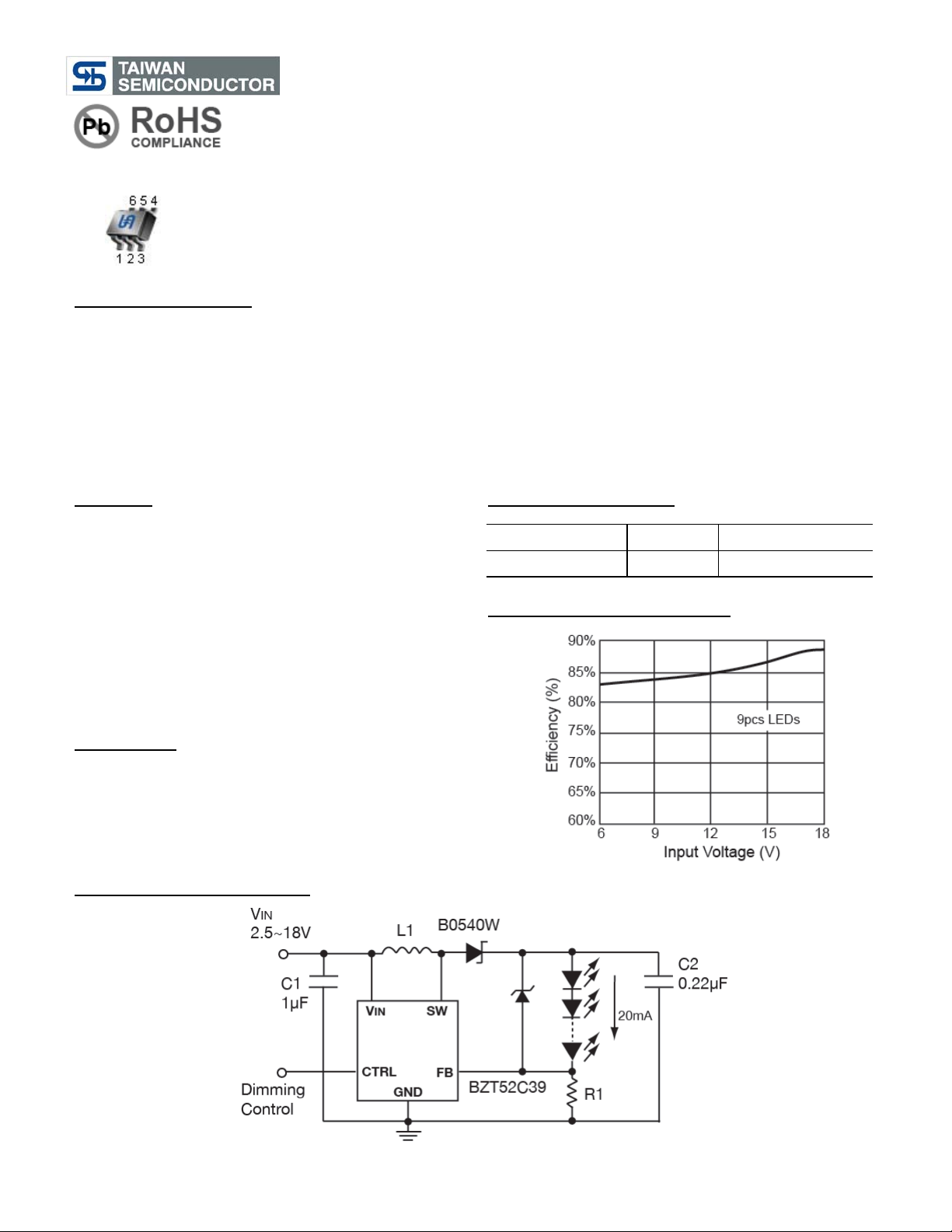
The TS19370 is a step-up DC/DC converter specifically designed to drive white LEDs with a constant current. The
device can drive 2 ~ 9 LEDs in series from a Li-Ion cell. Series connection of the LEDs provides identical LED
currents resulting in uniform brightness and eliminating the need for ballast resistors. The output capacitor can be as
small as 0.22µF, saving space versus alternative solutions. A low 95mV feedback voltage minimizes power loss for
better efficiency. Additional feature include over output voltage limiting when LEDs are disconnected.
The TS19370 switches at a fixed frequency of 1.2MHz, allowing the use of tiny, low profile inductors and capacitors to
minimize footprint and cost in space consideration applications for cellular phone backlighting or other hand held
equipment.
Ordering Information
Part No.
Package
Packing
TS19370CX6 RF
SOT-26
3Kpcs / 7” Reel
Features
● Inherently Matched LED Current
● High Efficiency: 88% Typical
● Drives Up to 6 LEDs @ Vin 5V
● Drives Up to 9 LEDs @ Vin 9~15V
● Over Output Voltage Protection 30V
● Fast 1.2MHz Switching Frequency
● Requires Only 0.22µF Output Capacitor
● PWM dimming control 1KHz to 10KHz
● Analog dimming control
Application
● Cellular Phones
● Portable Electronics Devices PDA, GPS
● LCD Display Module
● White LED Backlighting
Input Voltage vs. Efficiency
Typical Application Circuit
Pin Definition:
1. SW
6. Input
2. Ground
5. OVP
3. Feedback
4. CTRL
Boost (Step-up) WLED Driver with OVP
1/8 Version: D08

Parameter
Symbol
Limit
Unit
Input Voltage
VIN
20
V
Supply Voltage (Recommended)
VIN
2.5 ~ 18
V
FB Voltage
VFB
10
V
SW Voltage
VSW
36
V
CTRL Voltage
V
CTRL
10
V
Ambient Temperature Range
TA
-40 to +85
o
C
Junction Temperature Range
TJ
-40 to +125
o
C
Function Parameter
Symbol
Test Conditions
Min
Typ
Max
Units
Input Voltage Range
VIN 2.5
--
18
V
Feedback Voltage
VFB
ISW=100mA, 66% duty
cycle
86
95
104
mV
FB Pin Bias Current
IB 10
45
100
nA
--
1.9
2.5
mA
Supply Current
IQ
CTRL = 0V
--
0.1
1.0
uA
Switching Frequency
F
RSW
0.8
1.2
1.6
MHz
Switch Current Limit
ICL --
320
--
mA
Maximum Duty Cycle
D
TMX
85
90
--
%
Switch V
CESAT
V
SAT
At ISW= 250mA
--
350
--
mV
Switch Leakage Current
I
LKG
VSW = 5V
--
0.01 5 µA
High
1.5
--
--
V
V
CTRL
V
CTL
Low
--
--
0.4
V
CTRL Pin Bias Current
I
CTL
Ctrl = 2V
--
65
--
µA
Over Voltage Protection
OVP
--
30
--
V
Thermal Resistance
θJA --
220
--
°C/W
Absolute Maximum Rating
TS19370
Boost (Step-up) WLED Driver with OVP
Electrical Specifications (Ta = 25
o
C, VIN= V
=3V, CIN=1uF, C
CTRL
=0.22uF unless otherwise noted)
OUT
Note:
Absolute maximum ratings are limits beyond which damage to the device may occur.
The maximum allowable power dissipation is a function of maximum function temperature, TJ(max), the junction to
ambient thermal resistance, θ JA , and the ambient temperature. The maximum allowable, power dissipation at any
ambient temperature is calculated using: PD(MAX)= [TJ(max)-TA]/θJA . Exceeding the maximum allowable power
dissipation will cause excessive die temperature. All limits at temperature extremes are guaranteed via correlation
using standard statistical methods
2/8 Version: D08

Pin
Function
Description
1
SW
Switching Pin. This is the collector of the internal NPN power switch. Connect to
inductor and diode. Minimize the metal trace area connected to this pin to reduce
EMI.
2
Ground
Ground Pin. Connect directly to local ground plane.
3
Feedback
Feedback Pin. Reference voltage is 95mV. Connect LEDs and a resistor at this pin.
LED current is determined by the resistance and CTRL voltage.
4
CTRL
Shutdown Pin and Dimming Control Pin.
VCTRL > 1.8V generates full-scale LED current
VCTRL < 0.4V chip is off
Switching from 04V to 2.0V, PWM duty cycle controls the LED current
5
OVP
Over Voltage Protection, 30V
6
Input
Input Supply Pin. Bypass this pin with a capacitor as close to the device as possible
Functional Block
TS19370
Boost (Step-up) WLED Driver with OVP
Pin Description
3/8 Version: D08

TS19370
Boost (Step-up) WLED Driver with OVP
Application Information
Operation
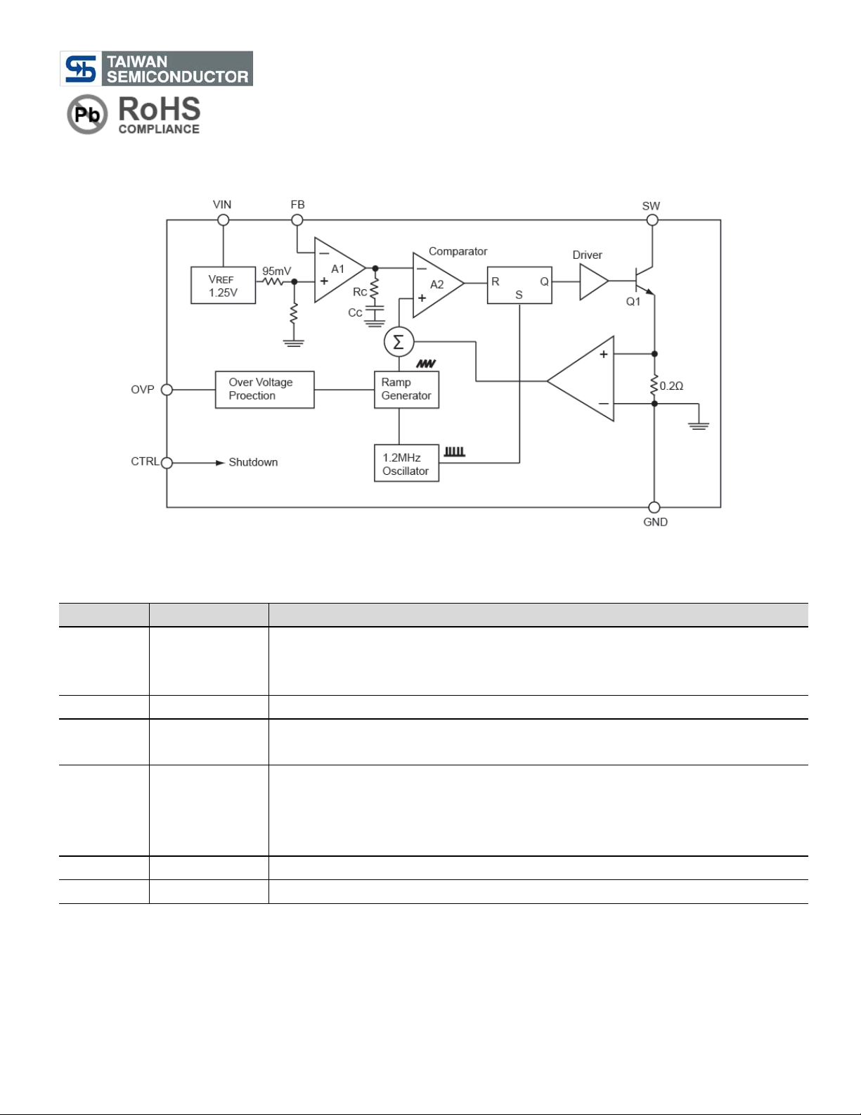
The TS19370 uses a constant frequency, current mode control scheme to provide excellent line and load regulation.
Operation can be best understood by referring to the block diagram. At the start of each oscillator cycle, the RS latch is
set, which turns on the power switch Q1. A voltage proportional to the switch current is added to a stabilizing ramp and
the resulting sum is fed into the positive terminal of the PWM comparator A2. When this voltage exceeds the level at
the negative input of A2, the RS latch is reset turning off the power switch. The level at the negative input of A2 is set
by the error amplifier A1, and is simply an amplified version of the difference between the feedback voltage and the
reference voltage of 95mV. In this manner, the error amplifier sets the correct peak current level to keep the output in
regulation. If the error amplifier’s output increases, more current is delivered to the output; if it decreases, less current
is delivered.
Minimum Output Current
The TS19370 can regulate three series LEDs connected at low output currents, down to approximately 4mA from a
4.2V supply, without pulse skipping, using the same external components as specified for 20mA operation. As the
current is further reduced, the device will begin skipping pulses. This will result in some low frequency ripple, although
the LED current remains regulated on an average basis down to zero.
Soft Start and Current Limit
The internal soft start circuit minimizes the inrush current during turning on TS19370. The Typical switch current is
limited to about 320mA by the chip.
Over Voltage Protection
The TS19370 has design an internal latched off open-circuit protection circuit, the additional sense pin to detect the
voltage when the LEDs are disconnected from the circuit or fail open, the TS19370 will shutdown until input condition
changes to bring it out of the shutdown mode.
Inductor Selection
A 22µH inductor is recommended for most TS19370 applications. Although small size and high efficiency are major
concerns, the inductor should have low core losses at 1.2MHz and low DCR (copper wire resistance).
Diode Selection
To maintain high efficiency, the average current rating of the Schottky diode should be large than the peak inductor
current, IPK. Schottky diode with a low forward drop and fast switching speeds are ideal for increase efficiency in
portable application. Choose a reverse breakdown of the Schottky diode large than the output voltage. A Schottky
diode rated at 100mA to 200mA is sufficient for most TS19370 applications.
Capacitor Selection
The small size of ceramic capacitors makes them ideal for TS19370 applications. X5R and X7R types are
recommended because they retain their capacitance over wider voltage and temperature ranges than other types such
as Y5V or Z5U. A 1µF input capacitor and a 0.22µF output capacitor are sufficient for most.
4/8 Version: D08

TS19370
ILED (mA)
R1(Ω)
5
19.1
10
9.53
12
7.87
15
6.34
20
4.75
Dimming Control using a DC Voltage
VDC(V)
VFB
Iout(mA)
2 0 0
1.8
2.2
0.43
1.6
9.2
1.8
1.4
19.6
3.6
1.2
31.1
6
1
43.4
8.5
0.8
63
12.3
0.6
74
14.5
0.4
86.4
16.9
0.2
96.9
19
0
102
20
Boost (Step-up) WLED Driver with OVP
Application Information (Continue)
LED Current Control
The LED current is controlled by the feedback resistor (R1). The feedback reference is 95mV. The LED current is
95mV/R1. In order to have accurate LED current, precision resistors are preferred (1% is recommended). The formula
and table 3 for R1 selection are shown below.
R1 = 95mV/ILED
LED Dimming Control
There are some different types of dimming control circuits:
1. Using a PWM Signal to SHDN Pin
With the PWM signal applied to the SHDN pin, the TS19370 is turned on or off by the PWM signal. The LEDs operate
at either zero or full current. The average LED current increases proportionally with the duty cycle of the PWM signal. A
0% duty cycle will turn off the TS19370 and corresponds to zero LED current. A 100% duty cycle corresponds to full
current. The typical frequency range of the PWM signal is 1kHz to 10kHz.
The magnitude of the PWM signal should be higher than the minimum SHDN voltage high.
For some applications, the preferred method of brightness control is a variable DC voltage to adjust the LED current.
The dimming control using a DC voltage is shown in Figure 4. As the DC voltage increases, the voltage drop on R2
increases and the voltage drop on R1 decreases. Thus, the LED current decreases. The selection of R2 and R3 will
make the current from the variable DC source much smaller than the LED current and much larger than the FB pin bias
current. For VDC range from 0V to 2V, the selection of resistors in Figure 4 gives dimming control of LED current from
0mA to 20mA.
5/8 Version: D08

TS19370
Dimming Control using a Filtered PWM Signal
Duty
Iout ( mA)
0%
20
20%
17.4
30%
15
40%
12.4
50%
10
60%
8
70%
6.4
80%
4.07
100%
0
PWM : 2V ; 1KHz ; Vin=3.6V
Boost (Step-up) WLED Driver with OVP
Application Information (Continue)
2. Using a Filtered PWM Signal
The filtered PWM signal can be considered as an adjustable DC voltage. It can be used to replace the variable DC
voltage source in dimming control. The circuit is shown as follow:
6/8 Version: D08

TS19370
SOT-26 Mechanical Drawing
70
= Device Code
Y
= Year Code
M
= Month Code
(A=Jan, B=Feb, C=Mar, D=Apl, E=May, F=Jun, G=Jul, H=Aug,
I=Sep, J=Oct, K=Nov, L=Dec)
L
= Lot Code
SOT-26 DIMENSION
MILLIMETERS
INCHES
DIM
MIN
TYP
MAX
MIN
TYP
MAX
A
0.95 BSC
0.0374 BSC
A1
1.9 BSC
0.0748 BSC
B
2.60
2.80
3.00
0.1024
0.1102
0.1181
C
1.40
1.50
1.70
0.0551
0.0591
0.0669
D
2.80
2.90
3.10
0.1101
0.1142
0.1220
E
1.00
1.10
1.20
0.0394
0.0433
0.0472
F
0.00
--
0.10
0.00
0.0039
G
0.35
0.40
0.50
0.0138
0.0157
0.0197
H
0.10
0.15
0.20
0.0039
0.0059
0.0079
I
0.30
--
0.60
0.0118
--
0.0236
J
5º
--
10º
5º
--
10º
Boost (Step-up) WLED Driver with OVP
Marking Diagram
7/8 Version: D08

TS19370
Boost (Step-up) WLED Driver with OVP
Notice
Specifications of the products displayed herein are subject to change without notice. TSC or anyone on its behalf,
assumes no responsibility or liability for any errors or inaccuracies.
Information contained herein is intended to provide a product description only. No license, express or implied, to any
intellectual property rights is granted by this document. Except as provided in TSC’s terms and conditions of sale for
such products, TSC assumes no liability whatsoever, and disclaims any express or implied warranty, relating to sale
and/or use of TSC products including liability or warranties relating to fitness for a particular purpose, merchantability,
or infringement of any patent, copyright, or other intellectual property right.
The products shown herein are not designed for use in medical, life-saving, or life-sustaining applications. Customers
using or selling these products for use in such applications do so at their own risk and agree to fully indemnify TSC for
any damages resulting from such improper use or sale.
8/8 Version: D08
 Loading...