现货库存、技术资料、百科信息、热点资讯,精彩尽在鼎好!
-
Voltage Comparator
Voltage Comparator
General Description
• The TCI LM393 consist of two independent voltage
comparator, designed specifically to operate from a single
power supply over a wide voltage range.
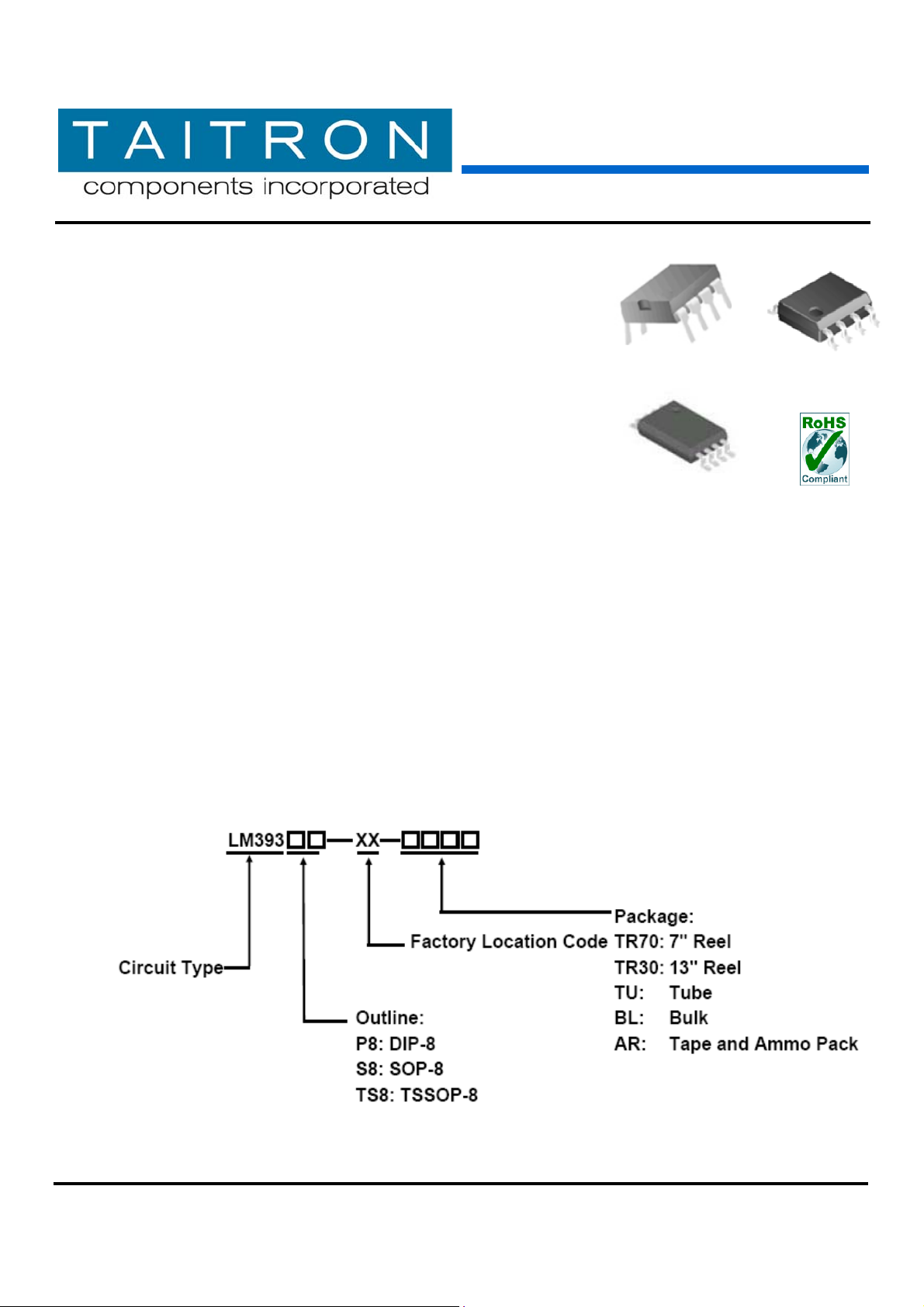
• The LM393 is available in standard DIP-8, SOP-8
and TSSOP-8 packages.
.
Features Applications
• Single or dual supply operation
• Wide operating supply range
CC=2V ~ 36V or ±1 ~ ±18V)
(V
• Input common-mode voltage includes ground
• Low supply current drain I
• Low input bias current I
• Output compatible with TTL, DTL, and CMOS logic system
• RoHS Compliance
CC=0.8mA (Typical)
BIAS=25nA (Typical)
• Battery Charger
• Cordless Telephone
• Switching Power Supply
• PC Motherboard
• Communication Equipment
DIP-8
TSSOP-8
LM393
SOP-8
Ordering Information
TAITRON COMPONENTS INCORPORATED www.taitroncomponents.com
Tel: (800)
Fax: (800)-TAITFAX (800)-824-8329 (661)-257-6415
TAITRON (800)-824-8766 (661)-257-6060
Rev. A/DX 2007-06-04
Page 1 of 11

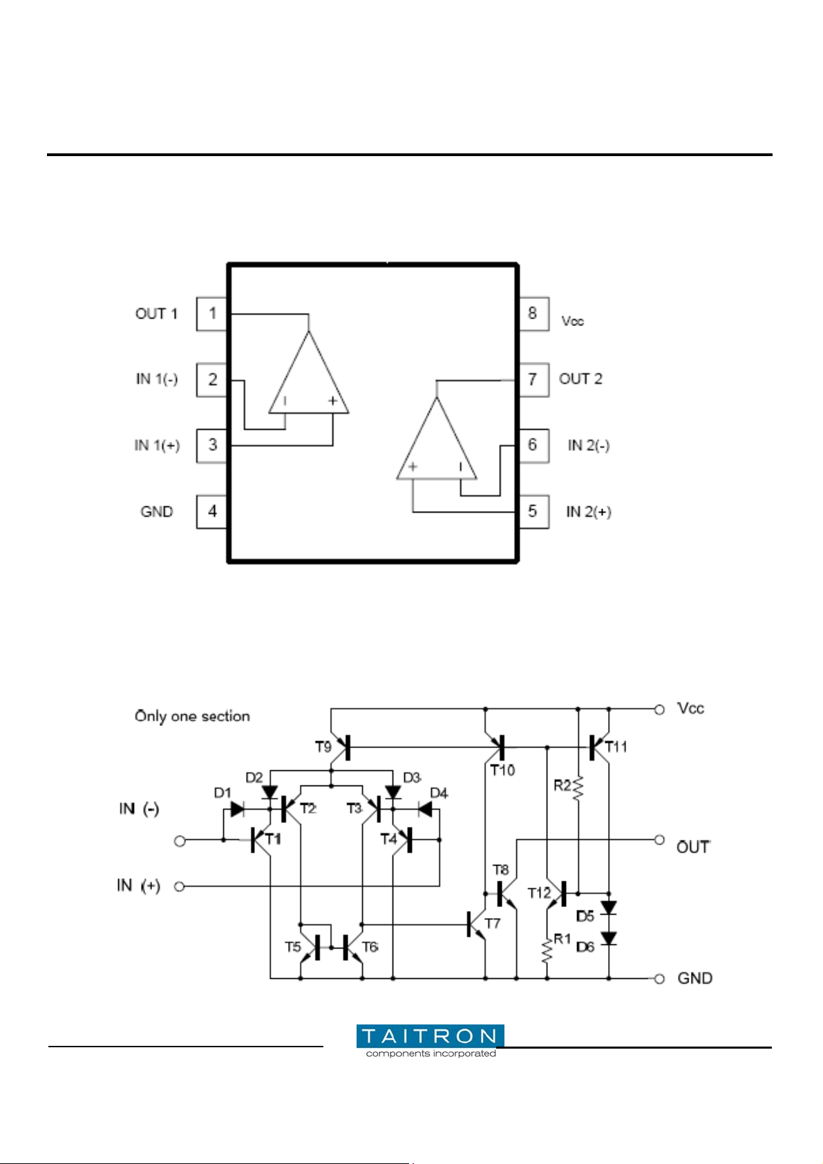
Pin Configuration
Voltage Comparator
LM393
Block Diagram
Rev. A/DX 2007-06-04
www.taitroncomponents.com
Page 2 of 11

Voltage Comparator
Absolute Maximum Ratings
Symbol Description LM393 Unit
LM393
VCC
VI(DIFF)
VIN
Supply Voltage
±18 or 36
Differential Input Voltage 36 V
Input Voltage -0.3 ~ 36 V
V
TSSOP-8 570
PD
Power
Dissipation
SOP-8 660
mW
DIP-8 780
TJ
TOPR
TSTG
Operating Junction Temperature 150 ° C
Operating Temperature Range -40 ~ 85 ° C
Storage Temperature Range -65 ~ 150 ° C
Note: Absolute maximum ratings are those valu es beyond which the devi ce coul d be perma ne ntly dam aged.
Absolute maximum ratings are stress ratings only and functional device operation is not implied.
Electrical Characteristics
(V
CC=5.0V, T
Symbol Description
VI(OFF)
VSAT
VI(CM)
=25ºC, all voltage referenced to GND unless otherwise specified)
A
Input Offset Voltage - 1.0 5.0 mV
Output Saturation Voltage - 160 400 mV V
Input Common Mode Voltage 0 -
LM393
Min. Typ. Max.
VCC
Unit Conditions
CM=0V to VCC-1.5V
V
O(P)=1.4V,RS=0Ω
V
I(-)>1V, VI(+)=0V, ISINK=4mA
-1.5
V VCC=30V
GV
ICC
II(OFF)
II(BIAS)
IO(SINK)
IO(LEAK) Output Leakage Current
tR
tR
www.taitroncomponents.com
Large Signal Voltage Gain 50 200 - V/mV
Power Supply Current
- 0.8 2.5 RL=∞, VCC=30V
mA
- 0.6 1.0
V
CC=15V, RL≥15KΩ
L=∞
R
Input Offset Current - 5 50 nA Input Bias Current - 65 250 nA Output Sink Current 6 18 - mA V
I(-)>1V, VI(+)=0V, VO(P)<1.5V
- 0.1 - nA VI(+)=1V, VI(-)=0V, VO(P)=5V
- - 1.0
µA
Large Signal Response Time - 350 - ns
V
I(+)=1V, VI(-)=0V, VO(P)=30V
IN=TTL logic wing,
V
REF=1.4V,VRL=5V, RL=5.1KΩ
V
Response Time - 1400 - ns VRL=5V, RL=5.1KΩ
Rev. A/DX 2007-06-04
Page 3 of 11

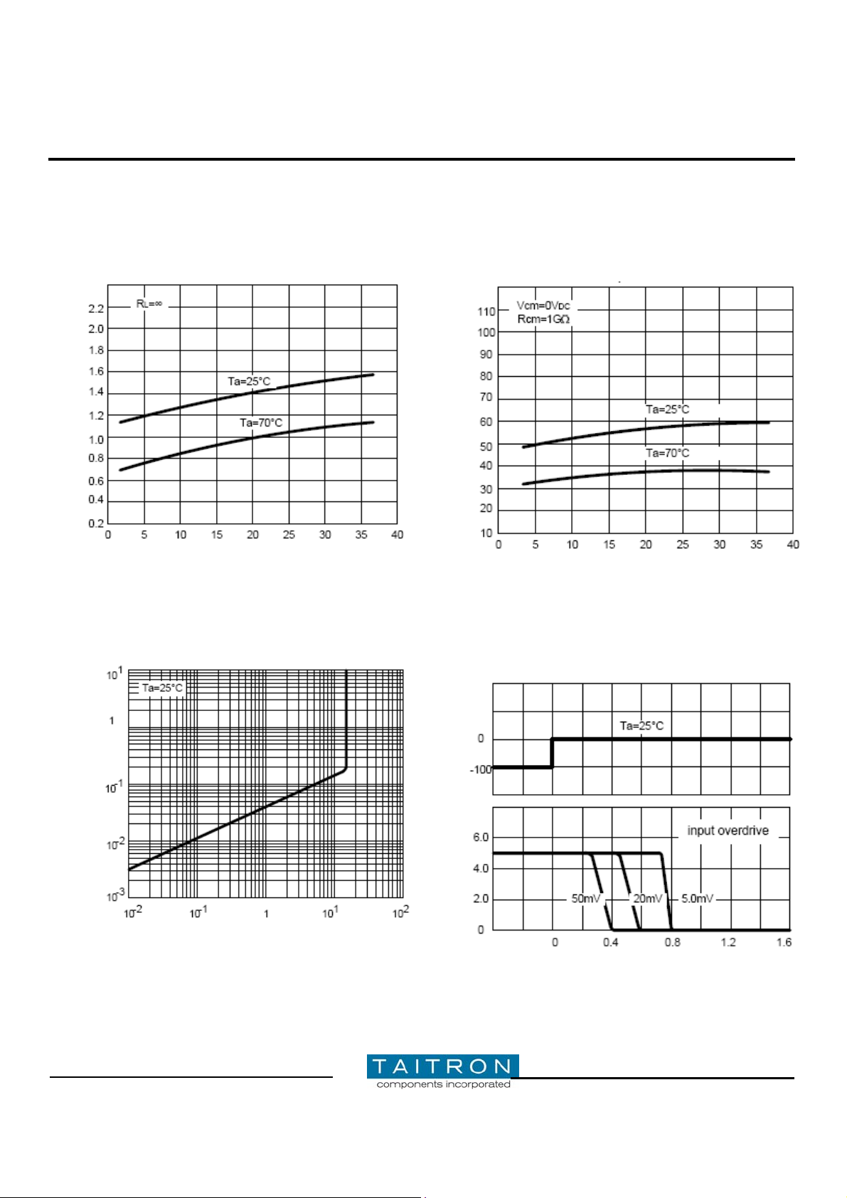
Typical Characteristics Curves
Voltage Comparator
LM393
Supply Current (mA)
Fig.1- Supply Current
Supply Voltage (V)
Fig.3- Output Saturation Voltage
Fig.2- Input Current
Input Current (nA)
Supply Voltage (V)
Fig.4- Response Time for Various Input
Overdrive Negative Transition
Input Voltage (mV)
Saturation Voltage (V)
Output Sink Current (mA)
Output Voltage (V)
Rev. A/DX 2007-06-04
www.taitroncomponents.com
Page 4 of 11

Typical Characteristics Curves (Continued)
Fig.5- Response Time for Various Input
Overdrive Positive Transition
Input Voltage (mV) Output Voltage (V)
Time (µs)
Fig.7- Voltage Follower Pulse Response
(small signal)
Output Voltage (V)
Time (µs)
Voltage Comparator
Fig.6- Voltage Follower Pulse Response
Input Voltage (V) Output Voltage (V)
Time (µs)
Fig.8- Large Signal Frequency Response
Output Swing (Vp-p)
Frequency (Hz)
LM393
Rev. A/DX 2007-06-04
www.taitroncomponents.com
Page 5 of 11

Typical Characteristics Curves (Continued)
Fig.9- Output Characteristics Current Sourcing
Output Reference VCC (V)
Output Source Current (mA)
Fig.11- Current Limiting
Output Voltage (V)
Temperature (° C)
Voltage Comparator
LM393
Fig.10- Output Characteristics Current Sinking
Output Voltage (V)
Output Sink Current (mA)
Rev. A/DX 2007-06-04
www.taitroncomponents.com
Page 6 of 11

Typical Applications
Fig.12-Basic Comparator
Fig.14-One Shot Multivibrator
Voltage Comparator
LM393
Fig.13-Driving CMOS
Fig.15-Suqarewave Oscillator
Rev. A/DX 2007-06-04
www.taitroncomponents.com
Page 7 of 11

Dimensions in mm (inches)
Voltage Comparator
LM393
DIP-8
Rev. A/DX 2007-06-04
www.taitroncomponents.com
Page 8 of 11

Voltage Comparator
LM393
SOP-8
Rev. A/DX 2007-06-04
www.taitroncomponents.com
Page 9 of 11

Voltage Comparator
LM393
TSSOP-8
Rev. A/DX 2007-06-04
www.taitroncomponents.com
Page 10 of 11

How to contact us:
28040 WEST HARRISON PARKAWAY, VALENCIA, CA 91355-4162
Voltage Comparator
US HEADQUARTERS
Tel: (800) TAITRON (800) 824-8766 (661) 257-6060
Fax: (800) TAITFAX (800) 824-8329 (661) 257-6415
Email: taitron@taitroncomponents.com
Http://www.taitroncomponents.com
LM393
TAITRON COMPONENTS MEXICO, S.A .DE C.V.
BOULEVARD CENTRAL 5000 INTERIOR 5 PARQUE INDUSTRIAL ATITALAQUIA, HIDALGO C.P.
42970 MEXICO
Tel: +52-55-5560-1519
Fax: +52-55-5560-2190
TAITRON COMPONETS INCORPORATED E REPRESENTAÇÕES DO BRASIL LTDA
RUA DOMINGOS DE MORAIS, 2777, 2.ANDAR, SALA 24 SAÚDE - SÃO PAULO-SP 04035-001 BRAZIL
Tel: +55-11-5574-7949
Fax: +55-11-5572-0052
TAITRON COMP O NE TS I NCORPORATED, SHAN GH A I RE P R ES ENTATIVE OFFICE
CROSS REGION PLAZA, 899 LINGLING ROAD, SUITE 18C, SHANGHAI, 200030, CHINA
Tel: +86-21-5424-9942
Fax: +86-21-5424-9931
Rev. A/DX 2007-06-04
www.taitroncomponents.com
Page 11 of 11
 Loading...