

Page 1
y
y
General-purpose Operational Amplifiers / Comparators
SIGNATURE SERIES
Comparators
LM393DT,LM393PT,LM393ST,LM393WDT,LM393WPT,
LM2903DT,LM2903PT,LM339DT,LM339PT,LM2901DT,LM2901PT
●Description
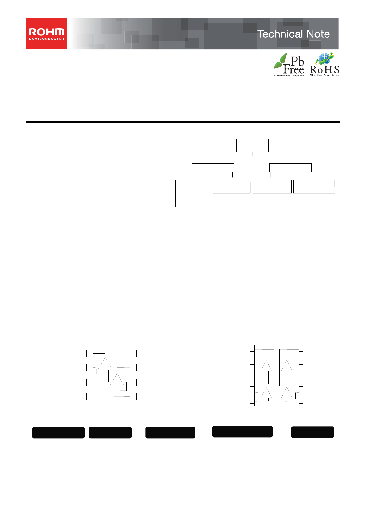
The Universal Standard LM393 / LM339 / LM2903 /
LM2901 family monolithic ICs integrate two / four
independent comparator circuits on a single chip and
feature high gain, low power consumption, and an
operating voltage range between 2[V] and 36[V]
(single power supply).
LM393 family LM339 family
LM393DT
LM393PT
LM393ST
LM393WDT
LM393WPT
●Features
1) Operating temperature range
Commercial Grade LM339/393 family : 0[℃] to + 70[℃]
Extended Industrial Grade LM2903/2901 family : -40[℃] to +125[℃]
2) Open collector output stage
3) Single / dual power supply compatible
4) Low supply current
0.4[mA] typ.(LM2903/393 family)
1.1[mA] typ.(LM2901/339 family)
5) Low input-bias current: 25[nA] typ.
6) Low input offset current: 5[nA] typ.
7) Common-mode input voltage range includes ground
8) Differential input voltage is possible to apply the absolute maximum ratings±36[V].
9) Low output saturation voltage
10) TTL, MOS, CMOS compatible output
●Pin Assignment
OUTPUT 1
INVERTING
INPUT 1
NON-INVERTING
INPUT 1
Vcc
1
2
-
+
3
―
4
+
-
―
8
Vcc
OUTPUT 2
7
INVERTING
6
INPUT 2
NON-INVERTING
5
INPUT 2
SO package8
LM393DT LM339DT LM339PTLM393PT
LM393WDT
LM2903DT LM2903PT
TSSOP8
LM393WPT LM2901DT LM2901PT
Mini SO8
LM393ST
Dual
LM2903 famil
LM2903DT
LM2903PT
INVERTING
NON-INVERTING
INPUT 1
INVERTING
NON-INVERTING
INPUT 2
SO package14
SIGNATURE
SERIES
LM339DT
LM339PT
1
OUTPUT 2
2
OUTPUT 1
-
3
Vcc
4
INPUT 1
5
6
INPUT 2
7
- +
- +
No.11094ECT04
Quad
LM2901 famil
LM2901DT
LM2901PT
14
OUTPUT 3
13
OUTPUT 4
-
Vcc
12
- +
- +
NON-INVERTING
11
INPUT 4
INVERTING
10
INPUT 4
NON-INVERTING
9
INPUT 3
INVERTING
8
INPUT 3
TSSOP14
www.rohm.com
© 2011 ROHM Co., Ltd. All rights reserved.
1/17
2011.06 - Rev.C
Page 2
LM393DT,LM393PT,LM393ST,LM393WDT,LM393WPT,
LM2903DT,LM2903PT,LM339DT,LM339PT,LM2901DT,LM2901PT
Technical Note
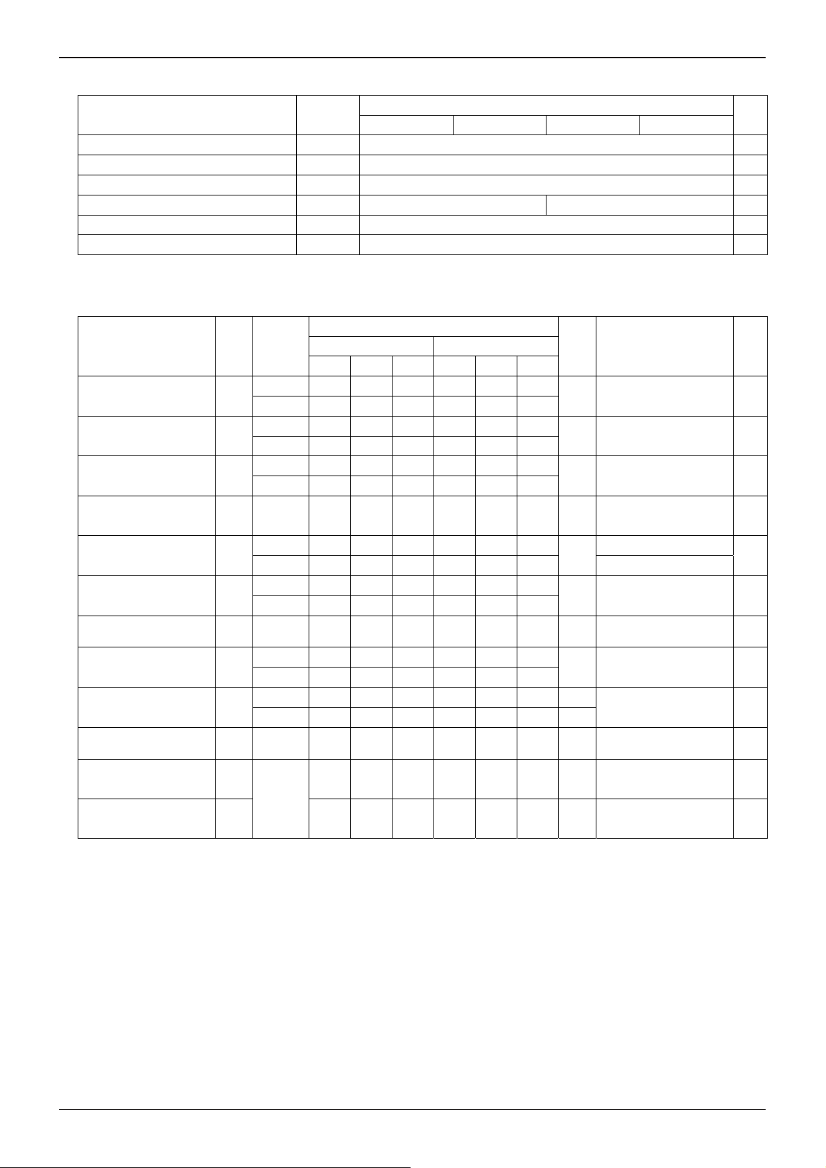
●Absolute Maximum Ratings (Ta=25℃)
Parameter Symbol
Supply Voltage Vcc+-Vcc
LM393 family LM339 family LM2903 family LM2901 family
-
Ratings
Unit
+36 V
Differential Input Voltage Vid ±36 V
Common-mode Input Voltage Range Vicm -0.3 to +36 V
Operating Temperature Range Topr 0 to +70 -40 to +125 ℃
Storage Temperature Range Tstg -65 to +150 ℃
Maximum Junction Temperature Tjmax +150 ℃
●Electric Characteristics
○LM393/339 family(Unless otherwise specified, Vcc
Parameter Symbol
Input Offset Voltage (*1) VIO
Input Offset Current (*1) IIO
Input Bias Current (*1) IIB
Large Signal Voltage Gain AVD
Supply Current
(All Comparators)
Input Common-mode
Voltage Range
Differential InputVoltage
Temperature
range
Min. Typ. Max. Min. Typ. Max.
25℃ - 1 7 - 1 7
full range - - 9 - - 9
25℃ - 5 50 - 5 50
full range - - 150 - - 150
25℃ - 25 250 - 25 250
full range - - 400 - - 400
25℃
ICC
VICM
VID 25℃ - - Vcc
25℃ - 0.4 1 - 1.1 2
full range - 1 2.5 - 1.3 2.5 Vcc+=30[V],no load
25℃ - - Vcc
full range - - Vcc+-2.0 - - Vcc+-2.0
25 200
+
=+5[V])
Limits
LM393 family LM339 family
25 200
-
+
-1.5 - - Vcc+-1.5
+
- - Vcc
Unit Conditions
+
Vcc
mV
nA VO=1.4[V] 2
nA VO=1.4[V] 2
V/mV
-
mA
V - 2
+
V -
=5 to 30[V],VO=1.4[V],
Vicm=0 to -1.5[V]
+
Vcc
=15[V],VO=1 to 11[V],
RL=15[kΩ]
+
Vcc
=5V,no load
Fig.
No.
2
2
3
-
Low level Output Voltage VOL
High level Output Current IOH
Output Sink Current
Small Single Response Time tRE
Large Single Response Time tREL - 300 - - 300 - ns
(*1) Absolute value
Isink 25℃ 6 16 - 6 16 - mA VID=-1[V],VO=1.5[V] 3
25℃ -
full range
25℃ -
full range
25℃
250 400
0.1
700
- -
1
- -
- -
- 1.3 - - 1.3 - μs
250 400
-
- -
0.1
- -
700
-
1 μA
mV VID=-1[V],Isink=4[mA] 3
nA
+
Vcc
=30[V],VID=1[V]
VO=30[V]
+
RL=5.1[kΩ], Vcc
VIN=100[mVp-p],
Overdrive=5[mV]
RL=5.1[kΩ], Vcc
VIN=TTL input, Vref=1.4[V]
=5[V]
+
=5[V]
3
3
3
www.rohm.com
© 2011 ROHM Co., Ltd. All rights reserved.
2/17
2011.06 - Rev.C
Page 3
LM393DT,LM393PT,LM393ST,LM393WDT,LM393WPT,
LM2903DT,LM2903PT,LM339DT,LM339PT,LM2901DT,LM2901PT
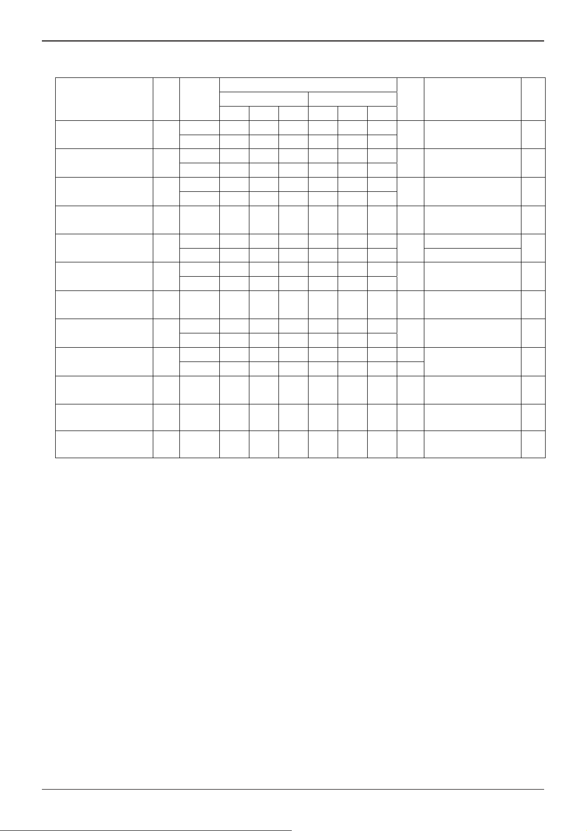
○LM2903/2901 family(Unless otherwise specified, Vcc+=+5[V])
Parameter Symbol
Input Offset Voltage (*2) VIO
Input Offset Current (*2) IIO
Input Bias Current (*2) IIB
Large Signal Voltage Gain AVD 25℃ 25 200 - 25 200 - V/mV
Supply Current
(All Comparators)
Input Common-mode
Voltage Range
Temperature
range
25℃ - 2 7 - 1 7
full range - - 15 - - 15
25℃ - 5 50 - 5 50
full range - - 150 - - 150
25℃ - 25 250 - 25 250
full range - - 400 - - 400
ICC
VICM
25℃ - 0.4 1 - 1.1 2
full range - 1 2.5 - 1.3 2.5 Vcc+=30[V],no load
25℃ - - Vcc
full range - - Vcc+-2.0 - - Vcc+-2.0
LM2903 family LM2901 family
Min. Typ. Max. Min. Typ. Max.
Limits
+
-1.5 - - Vcc+-1.5
Technical Note
Unit Conditions
+
=5 to 30[V],VO=1.4[V]
Vcc
mV
Vicm=0 to -1.5[V]
nA VO=1.4[V] 2
nA VO=1.4[V] 2
+
=15[V],VO=1 to 11[V],
Vcc
RL=15[kΩ]
+
Vcc
mA
V - 2
=5V,no load
Fig.
No.
2
2
3
Differential Input Vo ltage
Low Level Output Voltage VOL
High Level Output Current Isink
Output Sink Current
Small Single Response Time tRE 25℃ - 1.3 - - 1.3 - μs
Large Single Response Time tREL 25℃ - - 1.0 - - 1.0 μs
(*2) Absolute value
VID 25℃ - - Vcc
25℃ - 250 400 - 250 400
full range - - 700 - - 700
25℃ - 0.1 - - 0.1 - nA
full range - - 1 - - 1 μA
IOL 25℃ 6 16 - 6 16 - mA VID=-1[V],VO=1.5[V] 3
+
- - Vcc
+
V
mV VID=-1[V], Isink=4[mA] 3
+
Vcc
VO=30[V]
RL=5.1[kΩ], Vcc
VIN=100[mVp-p],
Overdrive=5[mV]
TTL input Vref=1.4[V]
RL=5.1[kΩ]
Output voltage at 95%
- -
=30[V],VID=1[V]
+
=5[V]
3
3
3
www.rohm.com
© 2011 ROHM Co., Ltd. All rights reserved.
3/17
2011.06 - Rev.C
Page 4
LM393DT,LM393PT,LM393ST,LM393WDT,LM393WPT,
y
y
y
y
y
y
y
y
LM2903DT,LM2903PT,LM339DT,LM339PT,LM2901DT,LM2901PT
Technical Note
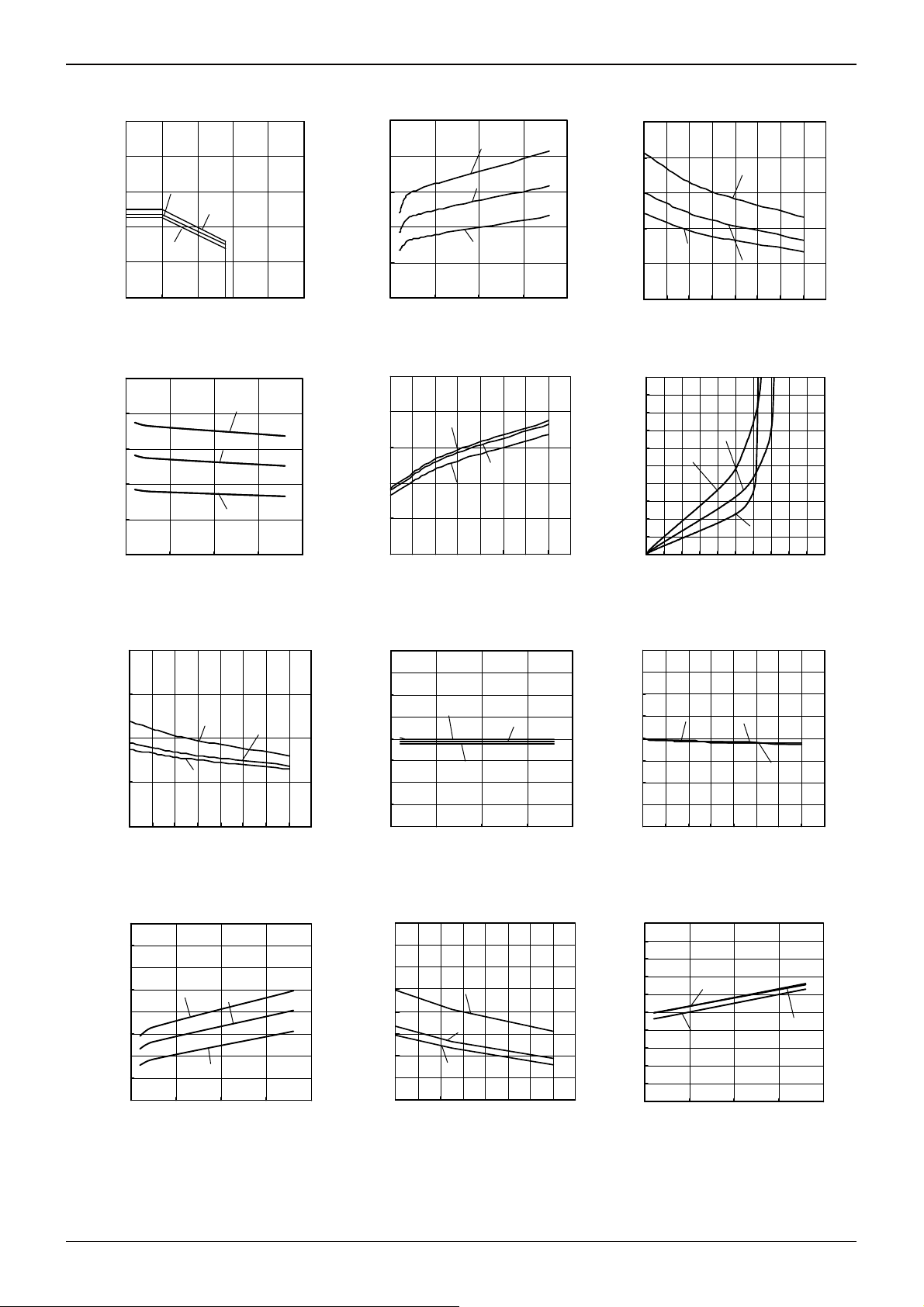
●Reference Data LM393 family
1000
800
600
400
200
POWER DISSIPATION [mW] .
LM393ST
LM393PT
LM393DT
LM393 famil
1
.
0.8
0.6
0.4
SUPPLY CURRENT [mA]
0.2
70℃
0
0255075100125
AMBIENT TE MP ER ATURE [℃] .
70
Fig.1 Fig.2 Fig. 3
Derating Curve
500
400
300
LM393 famil
70℃
25℃
0
0 10203040
SUPPLY VOLTAGE [V]
Supply Current – Supply Voltage
500
400
300
2V
200
100
OUTPUT SATURATION VOLTAGE [mV]
0
010203040
SUPPLY VOLTAGE [V]
Fig.4 Fig. 5 Fig. 6
Output Saturation Voltage
– Supply Voltage
40
0℃
(IOL=4[mA])
LM393 famil
30
36V
20
10
OUTPUT SINK CURRENT [mA]
0
0 1020304050607080
2V
AM BIE NT T EMP ERAT UR E [℃]
5V
Fig. 7 Fig. 8 Fig. 9
Output Sink Current – Ambient
160
140
120
100
80
60
40
INPUT BIAS CURRENT [nA]
20
0
010203040
Input Bias Current – Supply Voltage
(*)The data above is ability value of sample, it is not guaranteed. LM393family: 0[℃]~+70[℃]
Temperature
(VOUT=1.5[V])
0℃
70℃
SUPPLY VOLTAGE [V]
Fig. 10 Fig. 11 Fig. 12
LM393 famil
25℃
200
100
OUTPUT SATURATIO N VOLTAGE [mV]
0
01020304050607080
36V
AMBIENT TEMPERATURE [℃]
Output Saturation Voltage
– Ambient Temperature
8
6
4
2
0
-2
-4
INPUT OFFSET VOLTAGE [mV]
-6
-8
0 10203040
(IOL=4[mA])
0℃
70℃
SUPPLY VOLTAGE [V]
Input Offset Voltage – Supply Voltage
160
140
120
100
80
60
40
INPUT BIAS CURRENT [nA] .
20
0
01020304050607080
36V
5V
2V
AMBIENT TEMPERATURE [℃]
Input Bias Current – Ambient Temperature
0℃
25℃
LM393 famil
1
0.8
0.6
0.4
SUPPLY CURRENT [mA]
0.2
0
2V
0 1020304050607080
AMBIENT TEMPERATURE [℃]
LM393 family
36V
5V
LM393 famil
5V
Supply Current – Ambient Temperature
2.0
1.8
1.6
1.4
1.2
1.0
0.8
0.6
0.4
0.2
LOW LEVEL OUTPUT VOLTAGE [V]
0.0
0 2 4 6 8 101214161820
25℃
70℃
OUTPUT SINK CURRENT [mA]
LM393 family
0℃
Low Level Output Voltage
– Output Sink Current
(VCC=5[V])
2V
AMBIENT TEMPERATURE [℃]
LM393 family
5V
36V
25℃
LM393 famil
8
6
4
2
0
-2
-4
INPUT OFFSE T VO L TAG E [ m V]
-6
-8
0 1020304050607080
Input Offset Voltage – Ambient Temperature
LM393 family
50
40
30
20
10
0
-10
-20
-30
INPUT OFFSET CURRENT [ nA ]
-40
-50
0 10203040
LM393 famil
0℃
25℃
70℃
SUPPLY VOLTAGE [V]
Input Offset Current – Supply Voltage
www.rohm.com
© 2011 ROHM Co., Ltd. All rights reserved.
4/17
2011.06 - Rev.C
Page 5
LM393DT,LM393PT,LM393ST,LM393WDT,LM393WPT,
y
y
y
y
y
LM2903DT,LM2903PT,LM339DT,LM339PT,LM2901DT,LM2901PT
Technical Note
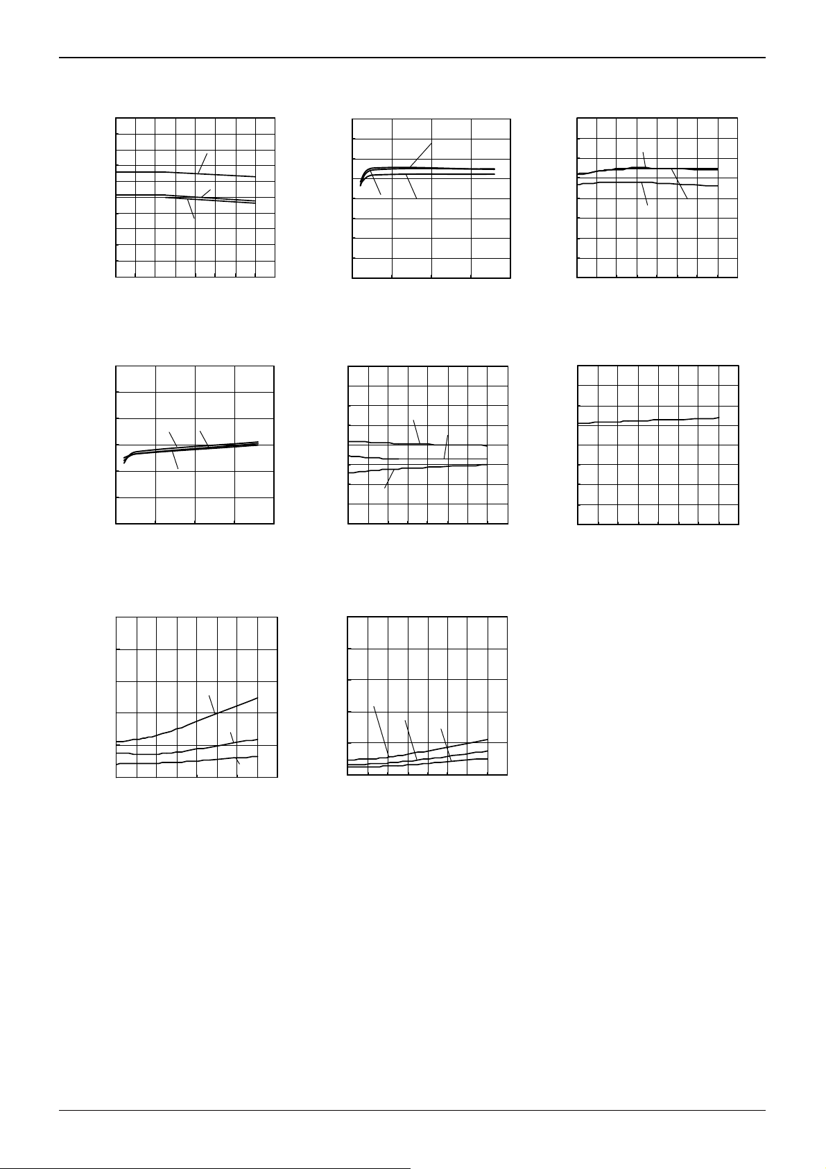
●Reference Data LM393 family
50
40
30
20
10
0
-10
-20
-30
INPUT O FFSET CU RRENT [nA]
-40
-50
0 1020304050 607080
AMBIE NT TEMPERATURE [℃]
Fig. 13 Fig. 14 Fig. 15
Input Offset Current – Ambient Temperature
160
140
120
.
100
80
60
COMMON MODE REJ E CT I O N RA T I O [ d B]
40
010203040
Common Mode Rejection Ratio
5
0℃
70℃
SUPPLY VOLTAGE [V]
Fig. 16 Fig. 17 Fig. 18
– Supply Voltage
4
2V
25℃
36V
5V
LM393 famil
LM393 famil
LM393 famil
140
130
120
110
100
LARGE SIGNAL VOLTAGE GAIN [dB] .
70℃
0℃
90
80
70
60
010203040
SUPPLY VOLTAGE [V]
LM393 family
25℃
Large Signal Voltage Gain
– Supply Voltage
140
130
120
110
100
90
80
70
POWER SUPPLY REJECTION RATIO [dB]
60
0 1020304050607080
36V
2V
AMBIENT TEMPERATURE [°C]
LM393 famil
5V
Common Mode Rejection Ratio
– Ambient Temperature
5
] .
s
4
LM393 famil
140
130
120
110
100
90
80
70
LARGE SIGNAL VOLTAGE GAIN [dB] .
60
01020304050607080
36V
2V
AMBIENT TEMPERA TURE [°C]
5V
Large Signal Voltage Gain
– Ambient Temperature
140
130
120
110
100
90
80
70
POWER SUPPLY REJECTION RATIO [dB] .
60
0 1020304050607080
AMBIENT TEMPERATURE [°C]
Power Supply Rejection Ratio
– Ambient Temperature
LM393 family
LM393 family
3
2
1
RESPONSE TIME (LOW to HIG H) [μs] . .
0
01020304050607080
AMBIENT TEMPERATURE [°C]
5mV overdrive
20mV overdrive
100mV overdrive
Fig. 19 Fig. 20
Response Time (Low to High)
– Ambient Temperature
(VCC=5[V],VRL=5[V],RL=5.1[kΩ])
3
5mV overdrive
2
1
RESPONSE TIME (HIGH to LOW) [μ
0
0 1020304050607080
20mV overdrive
100mV overdrive
AMBIENT TEMPERATURE [°C]
Response Time (High to Low)
–Ambient Temperature
(VCC=5[V],VRL=5[V],RL=5.1[kΩ])
(*)The data above is ability value of sample, it is not guaranteed. LM393family: 0[℃]~+70[℃]
www.rohm.com
© 2011 ROHM Co., Ltd. All rights reserved.
5/17
2011.06 - Rev.C
Page 6
LM393DT,LM393PT,LM393ST,LM393WDT,LM393WPT,
y
y
y
y
y
y
y
y
LM2903DT,LM2903PT,LM339DT,LM339PT,LM2901DT,LM2901PT
Technical Note
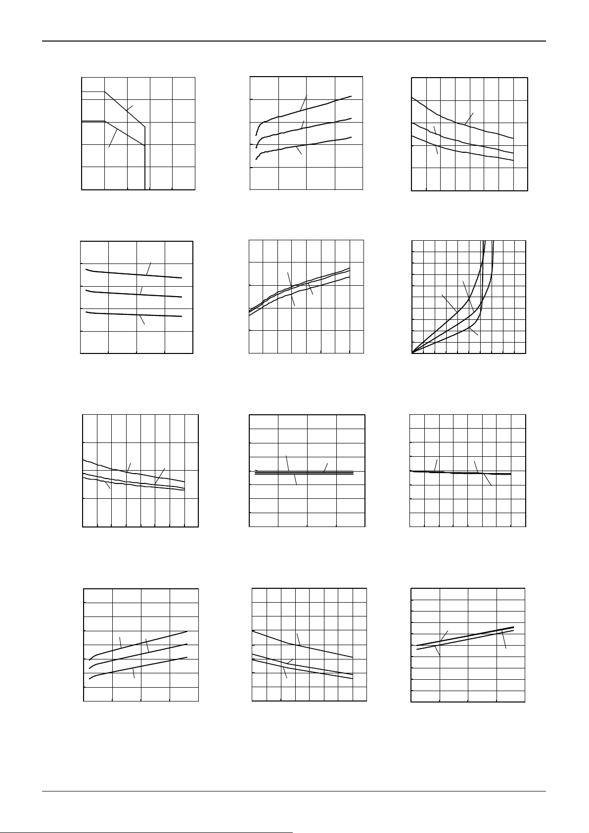
●Reference Data LM339 family
1000
800
600
400
200
POWER DISSIPATION [mW] .
LM339DT
LM339PT
LM339 famil
1
1
.
.
0.8
0.8
0.6
0.6
0.4
0.4
SUPPLY CURRENT [mA]
SUPPLY CURRENT [mA]
0.2
0.2
0℃
25℃
70℃
0
0255075100125
AMBIENT TE MP ER ATURE [℃] .
70
Fig.21 Fig.22 Fig. 23
Derating Curve
500
400
300
LM339 famil
70℃
25℃
200
100
OUTPUT SATURATION VOLTAGE [mV]
0
0 10203040
SUPPLY VOLTAGE [V]
Fig.24 Fig. 25 Fig. 26
Output Saturation Voltage
– Supply Voltage
40
0℃
(IOL=4[mA])
LM339 famil
30
36V
20
10
OUTPUT SINK CURRENT [mA]
0
0 1020304050607080
2V
AM BIE NT T EMP ERAT UR E [
5V
]
℃
Fig. 27 Fig. 28 Fig. 29
Output Sink Current – Ambient
160
140
120
100
80
60
40
INPUT BIAS CURRENT [nA]
20
0
010203040
Input Bias Current – Supply Voltage
(*)The data above is ability value of sample, it is not guaranteed. LM339family: 0[℃]~+70[℃]
Temperature
(VOUT=1.5[V])
0℃
70℃
SUPPLY VOLTAGE [V]
Fig. 30 Fig. 31 Fig. 32
LM339 famil
25℃
0
0
0 10203040
0 10203040
SUPPLY VOLTAGE [V]
SUPPLY VOLTAGE [V]
Supply Current – Supply Voltage
500
400
300
200
100
OUTPUT SATURATIO N VOLTAGE [mV]
0
01020304050607080
2V
5V
36V
AMBIENT TEMPERATURE [
Output Saturation Voltage
– Ambient Temperature
8
6
4
2
0
-2
-4
INPUT OFFSET VOLTAGE [mV]
-6
-8
0 10203040
(IOL=4[mA])
0℃
70℃
SUPPLY VOLTAGE [V]
Input Offset Voltage – Supply Voltage
160
140
120
100
80
60
40
INPUT BIAS CURRENT [nA] .
20
0
01020304050607080
36V
5V
2V
AMBIENT TEMPERATURE [
Input Bias Current – Ambient Temperature
LM339 famil
25℃
LM339 family
℃
]
LM339 famil
LM339 family
]
℃
36V
LM339 famil
]
℃
1
0.8
0.6
0.4
SUPPLY CURRENT [mA]
0.2
5V
2V
0
0 1020304050607080
AMBIENT TEMPERATURE [
Supply Current – Ambient Temperature
2.0
1.8
1.6
1.4
1.2
1.0
0.8
0.6
0.4
0.2
LOW LEVEL OUTPUT VOLTAGE [V]
0.0
0 2 4 6 8 101214161820
25℃
70℃
OUTPUT SI NK CURRE NT [mA]
LM339 family
0℃
Low Level Output Voltage
– Output Sink Current
8
(VCC=5[V])
6
4
2
0
-2
-4
INPUT OFFSE T VO L TAG E [ m V]
-6
-8
2V
0 1020304050607080
AMBIENT TEMPERATURE [
LM339 family
5V
36V
℃
]
Input Offset Voltage – Ambient Temperature
50
40
30
20
10
0
-10
-20
-30
INPUT OFFSET CURRENT [nA]
-40
-50
0 10203040
0℃
70℃
SUPPLY VOLTAGE [V]
LM339 famil
25℃
Input Offset Current – Supply Voltage
www.rohm.com
© 2011 ROHM Co., Ltd. All rights reserved.
6/17
2011.06 - Rev.C
Page 7
LM393DT,LM393PT,LM393ST,LM393WDT,LM393WPT,
y
y
y
y
y
LM2903DT,LM2903PT,LM339DT,LM339PT,LM2901DT,LM2901PT
Technical Note
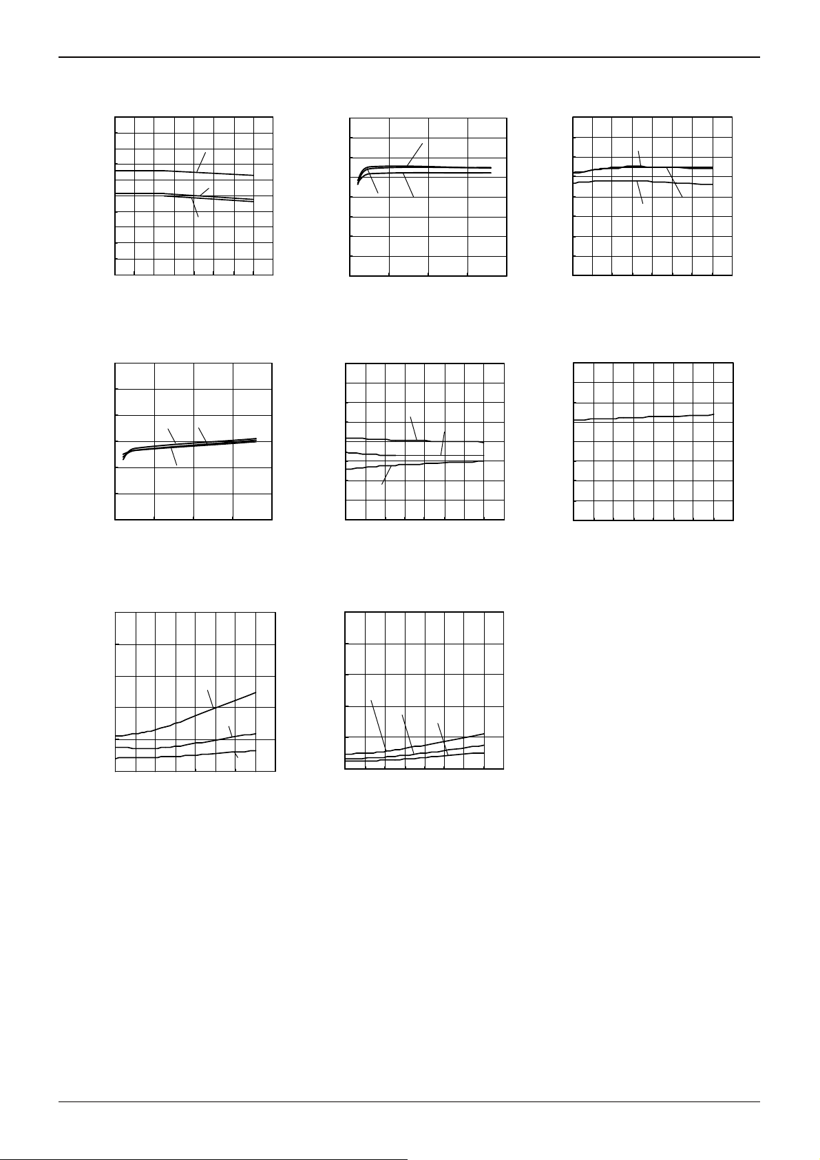
●Reference Data LM339 family
50
40
30
20
10
0
-10
-20
-30
INPUT O FFSET CU RRENT [nA ]
-40
-50
0 1020304050 607080
AMBIE NT TEMPERATURE [
Fig. 33 Fig. 34 Fig. 35
Input Offset Current – Ambient Temperature
160
140
120
.
100
80
60
COMMON MODE REJE CT ION RATIO[dB ]
40
010203040
5
0℃
70℃
SUPPLY VOLTAGE [V]
Fig. 36 Fig. 37 Fig. 38
Common Mode Rejection Ratio
– Supply Voltage
4
2V
25℃
36V
5V
LM339 famil
]
℃
LM339 famil
LM339 famil
140
130
120
110
100
LARGE SIGNAL VOLTAGE GAIN [dB] .
70℃
90
80
70
60
010203040
25℃
0℃
SUPPLY VOLTAGE [V]
LM339 family
Large Signal Voltage Gain
– Supply Voltage
140
130
120
110
100
90
80
70
POWER SUPPLY REJECTION RATIO [dB]
60
0 1020304050607080
36V
2V
AMBIENT TEMPERATURE [°C]
LM339 famil
5V
Common Mode Rejection Ratio
– Ambient Temperature
5
] .
s
4
LM339 famil
140
130
120
110
100
90
80
70
LARGE SIGNAL VOLTAGE GAIN [dB] .
60
01020304050607080
36V
5V
2V
AMBIENT TEMPERAT URE [°C]
Large Signal Voltage Gain
– Ambient Temperature
140
130
120
110
100
90
80
70
POWER SUPPLY REJECTION RATIO [dB] .
60
0 1020304050607080
AMBIENT TEMPERATURE [°C]
Power Supply Rejection Ratio
– Ambient Temperature
LM339 family
LM339 family
3
2
1
RESPONSE TIME (LOW to HIG H) [μs] . .
0
01020304050607080
AMBIENT TEMPERATURE [°C]
5mV overdrive
20mV overdrive
100mV overdrive
Fig. 39 Fig. 40
Response Time (Low to High)
– Ambient Temperature
(VCC=5[V],VRL=5[V],RL=5.1[kΩ])
3
5mV overdrive
2
1
RESPONSE TIME (HIGH to LOW) [μ
0
0 1020304050607080
20mV overdrive
100mV overdrive
AMBIENT TEMPERATURE [°C]
Response Time (High to Low)
–Ambient Temperature
(VCC=5[V],VRL=5[V],RL=5.1[kΩ])
(*)The data above is ability value of sample, it is not guaranteed. LM339family: 0[℃]~+70[℃]
www.rohm.com
© 2011 ROHM Co., Ltd. All rights reserved.
7/17
2011.06 - Rev.C
Page 8
LM393DT,LM393PT,LM393ST,LM393WDT,LM393WPT,
LM2903DT,LM2903PT,LM339DT,LM339PT,LM2901DT,LM2901PT
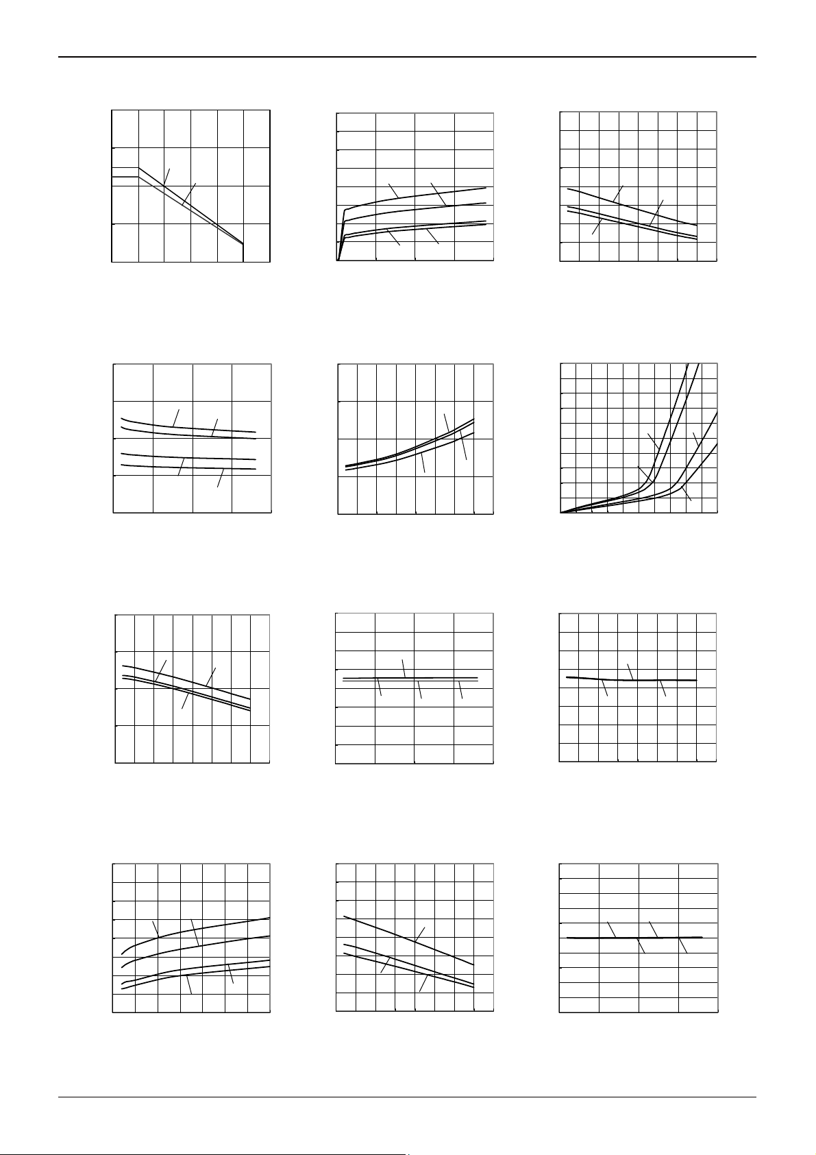
●Reference Data LM2903 family
800
1000
800
600
600
400
400
200
POWER DISSIPATION [mV]
200
POWER D ISSIP A TION Pd [m W ]
0
0
0 255075100125150
0 25 50 75 100 125 150
LM2903PT
AMBIENT TEMPERTURE [℃] .
AM B IENT TEMPERA TURE [℃]
Fig. 41 Fig. 42 Fig. 43
Derating Curve
LM2903 family
LM2903DT
1.6
1.4
1.2
1.0
0.8
0.6
0.4
SUPPLY CURRENT [mA ]
0.2
0.0
0 10203040
-40℃
SUPPLY VOLTAGE [V]
25℃
105℃
Supply Current – Supply Voltage
105℃
-40℃
36V
LM2903 family
LM2903 family
LM2903 family
105℃
200
150
100
50
MAXIMUM OUTPUT VOLTAGE [mV]
0
-50 -25 0 25 50 75 100 125 150
SUPPLY VOLTAGE [V]
36V
Output Saturation Voltage
– Ambient Temperature
(IOL=4[mA])
8
6
4
2
0
-2
-4
-6
INPUT OFFSET VOLTAGE [mV]
-8
0 10203040
-40℃
25℃
105℃
SUPPLY VOLTAGE [V]
Input Offset Voltage – Supply Voltage
160
140
120
100
80
60
40
INPUT BIAS CURRENT [nA]
20
0
-50 -25 0 25 50 75 100 125 150
5V
AMBIENT TEMPERATURE [℃]
36V
2V
Input Bias Current – Ambient Temperature
200
150
100
50
MAXIMUM OUTPUT VOLTAGE [mV]
0
0 10203040
Fig. 44 Fig. 45 Fig. 46
Output Saturation Voltage
40
125℃
25℃
SUPPLY VOLTAGE [V]
– Supply Voltage
(IOL=4[mA])
30
5V
20
2V
10
OUTPUT SINK CURRENT [mA]
0
-50 -25 0 25 50 75 100 125 150
AMBIENT TEMPERATURE [℃]
Fig. 47 Fig. 48 Fig. 49
Output Sink Current – Ambient
160
140
120
100
80
60
40
INPUT BIAS CURRENT [ n A ]
20
0
0 5 10 15 20 25 30 35
Input Bias Current – Supply Voltage
(*)The data above is ability value of sample, it is not guaranteed. LM2903family:-40[℃]~+125[℃]
Temperature
(VOUT=1.5[V])
-40℃
Fig. 50 Fig. 51 Fig. 52
25℃
125℃
SUPPLY VOLTAGE [V]
Technical Note
LM2903 family
125℃
1.6
1.4
1.2
1.0
0.8
0.6
0.4
SUPPLY CURRENT [mA]
0.2
0.0
-50 -25 0 25 50 75 100 125 150
36V
2V
AMBIENT TEMPERATURE [℃]
Supply Current – Ambient Temperature
LM2903 family LM2903 family
2V
5V
2
1.8
1.6
1.4
1.2
1
0.8
0.6
OUTPUT VOLTAGE [V]
0.4
0.2
0
0 2 4 6 8 101214161820
OUTPUT SINK CURRENT [mA]
105℃
Low Level Output Voltage
– Output Sink Current
LM2903 family
125℃
8
6
4
2
0
-2
-4
INPUT OFFSET VOLTAGE [mV]
-6
-8
-50 -25 0 25 50 75 100 125 150
(VCC=5[V])
2V
5V 36V
AMBIENT TEMPERATURE [℃]
Input Offset Voltage – Ambient Temperature
LM2903 family
50
40
30
20
10
0
-10
-20
-30
INPUT OFFSET CURRENT[nA]
-40
-50
0 10203040
SUPPLY VOLTAGE [V]
Input Offset Current – Supply Voltage
LM2903 family
5V
125℃
LM2903 family
LM2903 family
25℃ -40℃
105℃
25℃
-40℃
125℃
www.rohm.com
© 2011 ROHM Co., Ltd. All rights reserved.
8/17
2011.06 - Rev.C
Page 9
LM393DT,LM393PT,LM393ST,LM393WDT,LM393WPT,
LM2903DT,LM2903PT,LM339DT,LM339PT,LM2901DT,LM2901PT
Technical Note
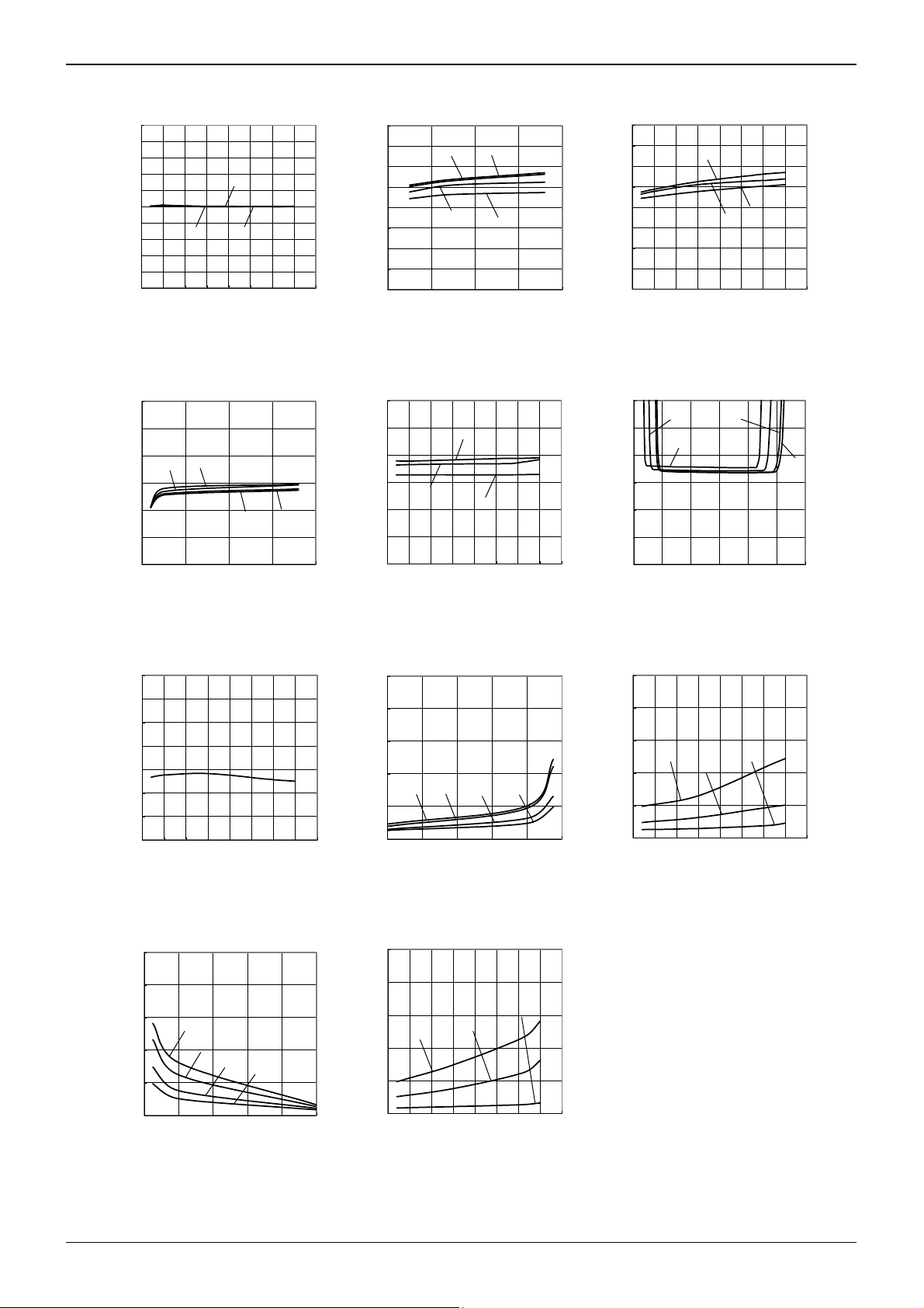
●Reference Data LM2903 family
15V
105℃
LM2903 family
5V
LM2903 family
LM2903 family
100mV
overdrive
125℃
2V
36V
-40℃
LM2903 family
LM2903 family
25℃
LM2903 family
LM2903 family
140
130
120
110
100
90
80
70
LARGE SINGAL VOLTAGE GAIN [dB]
60
0 10203040
125℃
25℃
SUPPLY VOLTAGE [V]
Large Signal Voltage Gain
– Supply Voltage
150
125
100
75
50
25
0
COMMON MODE REJECTION RATIO [dB]
-50 -25 0 25 50 75 100 125 150
AMBIENT TEMPERATURE [℃]
36V
5V
Common Mode Rejection Ratio
– Ambient Temperature
5
4
3
2
125℃
105℃
1
RESPONSE TIME (LOW TO HIGH)[μs]
0
-100 -80 -60 -40 -20 0
OVER DRIVE VOLTAGE [V]
Response Time (Low to High)
– Over Drive Voltage
(VCC=5[V],VRL=5[V],RL=5.1[kΩ])
5
50
40
30
20
10
0
-10
-20
-30
INPUT OFFSET CURRENT [nA]
-40
-50
-50 -25 0 25 50 75 100 125 150
5V
AMBIENT TEMPERATURE [℃]
Fig. 53 Fig. 54 Fig. 55
Input Offset Current – Ambient Temperature
160
140
120
100
125℃
105℃
80
60
40
COMMON MO DE RE J E CTION RATIO [d B]
0 10203040
SUPPLY VOLTAGE [V]
Fig. 56 Fig. 57 Fig. 58
Common Mode Rejection Ratio
– Supply Voltage
200
180
160
140
120
100
80
POWER SUPPLY REJECTION RATIO [dB]
60
-50 -25 0 25 50 75 100 125 150
AMBIENT TEMPERATURE [℃]
Fig. 59 Fig. 60 Fig. 61
Power Supply Rejection Ratio
– Ambient Temperature
5
LM2903 family
105℃
-40℃
140
130
120
110
100
90
80
70
LARGE SINGAL VOLTAGE GAIN [dB]
60
-50 -25 0 25 50 75 100 125 150
36V
AMBIENT TEMPERATURE [℃]
Large Signal Voltage Gain
– Ambient Temperature
LM2903 family
2V
6
25℃
4
2
0
-2
-4
INPUT OFFSET VOLTAGE [mV]
-6
-40℃
-1012345
INPUT VOLTAGE [V]
Input Offset Voltage – Input Voltage
(VCC=5V)
5mV overdrive
20mV overdrive
AMBIENT TEMPERATURE [℃]
– Ambient Temperature
25℃
LM2903 family
-40℃
LM2903 family
5
4
3
2
1
RRESPONSE TIME (LOW TO HIGH)[μs]
0
-50 -25 0 25 50 75 100 125 150
Response Time (Low to High)
(VCC=5[V],VRL=5[V],RL=5.1[kΩ])
4
3
2
1
RESPONSE TIME (HIGH TO LOW)[μs]
0
125℃
105℃
25℃
0 20 40 60 80 100
OVER DRIVE VOLTAGE [V]
Fig. 62 Fig. 63
Response Time (High to Low)
– Over Drive Voltage
(VCC=5[V],VRL=5[V],RL=5.1[kΩ])
-40℃
(*)The data above is ability value of sample, it is not guaranteed. LM2903family:-40[℃]~+125[℃]
4
3
5mV overdrive
2
1
RESPONSE TIME (HIGH TO LOW)[μs]
0
-50 -25 0 25 50 75 100 125 150
AMBIENT TEMPERATURE [℃]
100mV overdrive
20mV overdrive
Response Time (High to Low)
– Ambient Temperature
(VCC=5[V],VRL=5[V],RL=5.1[kΩ])
www.rohm.com
© 2011 ROHM Co., Ltd. All rights reserved.
9/17
2011.06 - Rev.C
Page 10
LM393DT,LM393PT,LM393ST,LM393WDT,LM393WPT,
y
y
y
y
y
y
y
y
y
y
y
LM2903DT,LM2903PT,LM339DT,LM339PT,LM2901DT,LM2901PT
Technical Note
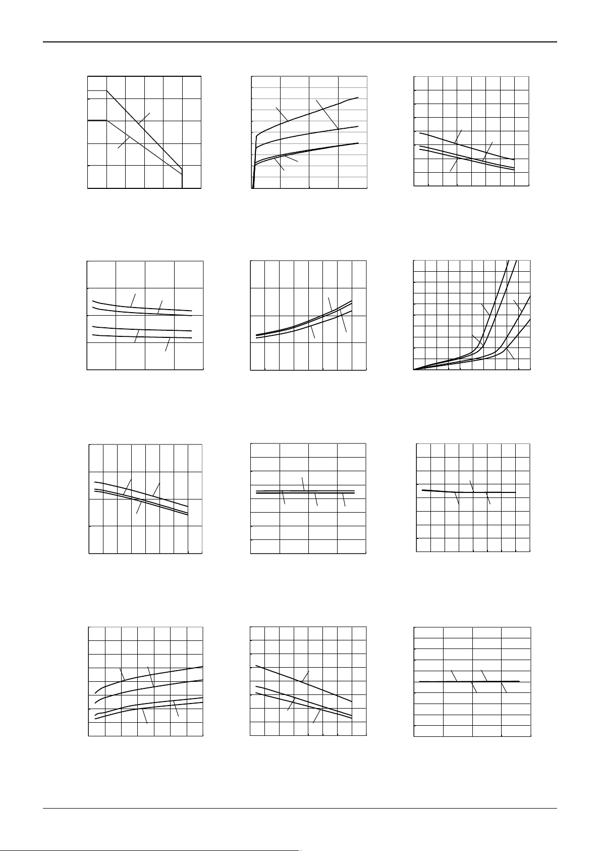
●Reference Data LM2901 family
1000
1000
800
800
600
600
400
POWER DISSIPATION [mW]
POWER D ISSIP A TION Pd [m W ]
400
200
200
LM2901DT
0
0
0 25 50 75 100 125 150
0 25 50 75 100 125 150
AMBIENT TEMPERATURE [℃]
AM B IEN T TE MPE RATU R E [℃ ]
Fig. 64 Fig. 65 Fig. 66
Derating Curve
200
LM2901PT
LM2901 famil
LM2901 family
2.0
1.8
1.6
-40℃
1.4
1.2
1.0
0.8
0.6
SUPPLY CURRENT [mA]
0.4
0.2
0.0
0 10203040
SUPPLY VOLTA GE [V]
25℃
125℃
105℃
Supply Current – Supply Voltage
200
150
100
125℃
105℃
150
100
50
MAXIMUM OUTPUT VOLTAGE [mV]
0
010203040
25℃
SUPPLY VOLTA GE [V]
-40℃
50
MAXIMUM OUTPUT VOLTAGE [mV]
0
-50 -25 0 25 50 75 100 125 1 50
SUPPLY VOLTAGE [V]
Fig. 67 Fig. 68 Fig. 69
Output Saturation Voltage
– Supply Voltage
(IOL=4[mA])
40
30
20
10
OUTPUT SINK CURRENT [mA]
0
-50 -25 0 25 50 75 100 125 150
AMBIENT TEMPERATURE [℃]
5V
2V
LM2901 famil
36V
Output Saturation Voltage
– Ambient Temperature
8
6
4
2
0
-2
-4
INPUT OFFSET VOLTAGE [mV]
-6
-8
0 10203040
25℃
SUPPLY VOLTAG E [V]
Fig. 70 Fig. 71 Fig. 72
Output Sink Current – Ambient Temperature
(VOUT=1.5[V])
Input Offset Voltage – Supply Voltage
160
140
120
100
80
60
40
INPUT BIAS CURRENT [nA]
20
-40℃
0
0 5 10 15 20 25 30 35
25℃
125℃
SUPPLY VOLTAGE [V]
LM2901 famil
105℃
160
140
120
100
80
60
40
INPUT BIAS CURRENT [nA]
20
0
-50 -25 0 25 50 75 100 125 150
5V
AMBIENT TEMPERATURE [℃]
Fig. 73 Fig. 74 Fig. 75
Input Bias Current – Supply Voltage
(*)The data above is ability value of sample, it is not guaranteed. LM2901family:-40[℃]~+125[℃]
Input Bias Current – Ambient Temperature
36V
(IOL=4[mA])
-40℃
105℃
36V
2V
2V
LM2901 famil
LM2901 famil
5V
LM2901 famil
125℃
LM2901 famil
1.6
1.4
1.2
1.0
0.8
0.6
0.4
SUPPLY CURRENT [mA]
0.2
0.0
-50 -25 0 25 50 75 100 125 150
AMBIENT TEMPERATURE [℃]
36V
2V
LM2901 famil
5V
Supply Current – Ambient Temperature
125℃
LM2901 famil
25℃
-40℃
2
1.8
1.6
1.4
1.2
1
0.8
0.6
OUTPUT VOLTAGE [V]
0.4
0.2
0
0 2 4 6 8 101214161820
OUTPUT SINK CURRENT [mA]
105℃
Low Level Output Voltage
– Output Sink Current
(VCC=5[V])
8
6
4
2
0
-2
-4
-6
INPUT OFFSET VOLTAGE [mV]
-8
-50 -25 0 25 50 75 100 125 150
AMBIENT TEMPERATURE [℃]
2V
5V
LM2901 famil
36V
Input Offset Voltage – Ambient Temperature
25℃
105℃
LM2901 famil
125℃
50
40
30
20
10
0
-10
-20
-30
INPUT OFFSET CURRENT[nA]
-40
-50
010203040
-40℃
SUPPLY VOLTAGE [V]
Input Offset Current – Supply Voltage
www.rohm.com
© 2011 ROHM Co., Ltd. All rights reserved.
10/17
2011.06 - Rev.C
Page 11

LM393DT,LM393PT,LM393ST,LM393WDT,LM393WPT,
y
y
y
y
y
y
y
y
y
y
y
LM2903DT,LM2903PT,LM339DT,LM339PT,LM2901DT,LM2901PT
Technical Note
●Reference Data LM2901 family
50
40
30
20
10
0
-10
-20
-30
INPUT OFFSET CURRENT [nA]
-40
-50
-50 -25 0 25 50 75 100 125 150
5V
AMBIENT TEMPERATURE [℃]
Fig. 76 Fig. 77 Fig. 78
Input Offset Current – Ambient Temperature
160
140
120
100
80
60
40
COMMON MO DE RE J E CTION RATIO [d B]
0 10203040
125℃
105℃
SUPPLY VOLTAGE [V]
Fig. 79 Fig. 80 Fig. 81
Common Mode Rejection Ratio
– Supply Voltage
200
180
160
140
120
100
80
POWER SUPPLY REJECTION RATIO [dB]
60
-50 -25 0 25 50 75 100 125 150
AMBIENT TEMPERATURE [℃]
Fig. 82 Fig. 83 Fig. 84
Power Supply Rejection Ratio
– Ambient Temperature
5
LM2901 famil
2V
36V
140
130
120
110
100
90
80
70
LARGE SINGAL VOLTAGE GAIN [dB]
60
0 10203040
125℃
25℃
SUPPLY VOLTAGE [V]
Large Signal Voltage Gain
-40℃
LM2901 famil
25℃
150
125
100
75
50
25
0
COMMON MODE REJECTION RATIO [dB]
-50 -25 0 25 50 75 100 125 150
– Supply Voltage
36V
5V
AMBIENT TEMPERATURE [℃]
Common Mode Rejection Ratio
– Ambient Temperature
LM2901 famil
LM2901 famil
5
4
3
2
1
RESPONSE TIME (LOW TO HIGH)[μs]
0
-100 -80 -60 -40 -20 0
Response Time (Low to High)
(VCC=5[V],VRL=5[V],RL=5.1[kΩ])
5
105℃
125℃
OVER DRIVE VOLTAGE [V]
– Over Drive Voltage
105℃
-40℃
2V
25℃ -40℃
LM2901 famil
LM2901 famil
LM2901 famil
LM2901 famil
140
130
120
110
100
90
80
70
LARGE SINGAL VOLTAGE GAIN [dB]
60
-50 -25 0 25 50 75 100 125 150
AMBIENT TEMPERATURE [℃]
36V
15V
Large Signal Voltage Gain
– Ambient Temperature
6
25℃
4
2
0
-2
-4
INPUT OFFSET VOLTAGE [mV]
-6
-40℃
-1012345
INPUT VOLTAGE [V]
Input Offset Voltage – Input Voltage
(VCC=5V)
5
4
3
5mV overdrive
2
1
RRESPONSE TIME (LOW TO HIGH)[μs]
0
-50 -25 0 25 50 75 100 125 150
20mV overdrive
AMBIENT TEMPERATURE [℃]
Response Time (Low to High)
– Ambient Temperature
(VCC=5[V],VRL=5[V],RL=5.1[kΩ])
LM2901 famil
5V
LM2901 famil
105℃
125℃
LM2901 famil
100mV overdrive
4
3
2
1
RESPONSE TIME (HIGH TO LOW)[μs]
0
125℃
105℃
25℃
-40℃
020406080100
OVER DRIVE VOLTAGE [V]
Fig. 85 Fig. 86
Response Time (High to Low)
– Over Drive Voltage
(VCC=5[V],VRL=5[V],RL=5.1[kΩ])
(*)The data above is ability value of sample, it is not guaranteed. BA2901: LM2901family:-40[℃]~+125[℃]
4
3
5mV overdrive
2
1
RESPONSE TIME (HIGH TO LOW)[μs]
0
-50 -25 0 25 50 75 100 125 150
AMBIENT TEMPERATURE [℃]
100mV overdrive
20mV overdrive
Response Time (High to Low)
– Ambient Temperature
(VCC=5[V],VRL=5[V],RL=5.1[kΩ])
www.rohm.com
© 2011 ROHM Co., Ltd. All rights reserved.
11/17
2011.06 - Rev.C
Page 12
LM393DT,LM393PT,LM393ST,LM393WDT,LM393WPT,
f
f
/Rf
f
A
LM2903DT,LM2903PT,LM339DT,LM339PT,LM2901DT,LM2901PT
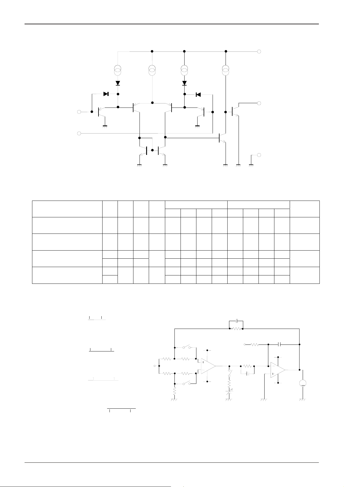
●Circuit Diagram
Non-inverting
input
Inverting
input
Fig.87 Circuit Diagram (each Comparator)
Technical Note
+
Vcc
V0
-
Vcc
●Measurement Circuit 1 NULL Method Measurement Condition
Parameter VF S1 S2 S3
Vcc+Vcc-EK Vicm Vcc+Vcc- EK Vicm
LM393/LM339 family LM2903/LM2901 family
+
,Vcc-,EK,Vicm unit:[V]
Vcc
Calculation
Input Offset Voltage VF1 ON ON ON 5 to 30 0 -1.4 0 5 to 30 0 -1.4 0 1
Input Offset Current VF2 OFF OFF ON 5 0 -1.4 0 5 0 -1.4 0 2
Input Bias Current
Large Signal Voltage Gain
VF3 OFF ON
VF4 ON OFF 5 0 -1.4 0 5 0 -1.4 0
VF5
ON ON ON
VF6 15 0 -11.4 0 15 0 -11.4 0
ON
5 0 -1.4 0 5 0 -1.4 0
15 0 -1.4 0 15 0 -1.4 0
-Calculation-
1.Input offset voltage (Vio)
Vio
VF1
1+
[V]
/Rs
R
2. Input offset current (Iio)
Iio
VF1VF2 -
/ Rs) Rf(1+ Ri
3. Input bias current (Ib)
Ib
2×
VF3VF4 -
(1+
Ri
4.Large signal voltage gain (Av)
V
10×
Log20×
[A]
[A]
/ Rs)
(1+
VF6 - VF5
/Rs)
S1
50[Ω]
RS
=
10[kΩ]
Ri
Vicm
RS
=
50[kΩ]
R
[dB]
=
Ri=10[kΩ]
50[Ω]
S2
Fig.88 Measurement Circuit 1 (each Comparator)
Vcc
DUT
Vcc
+
-
VRL
0.1[μF]
R
50[kΩ]
S3
RL
RK
EK
500[kΩ]0.1[μF]
500[kΩ]
RK
1000[pF]
+15[V]
NULL
-15[V]
3
4
V
VF
www.rohm.com
© 2011 ROHM Co., Ltd. All rights reserved.
12/17
2011.06 - Rev.C
Page 13

LM393DT,LM393PT,LM393ST,LM393WDT,LM393WPT,
A
A
OL/VO
LM2903DT,LM2903PT,LM339DT,LM339PT,LM2901DT,LM2901PT
Technical Note
●Measurement Circuit 2: Switch Condition
SW No.
SW
1
SW
2
SW
3
SW
4
SW
5
SW
6
SW
Supply Current ― OFF OFF OFF OFF OFF OFF OFF
Output Sink Current VOL=1.5[V] OFF ON ON OFF ON ON OFF
Saturation Voltage IOL=4[mA] OFF ON ON OFF OFF OFF ON
Output Leakage Current VOH=36[V] OFF ON ON OFF OFF OFF ON
Response Time
RL=5.1[kΩ]
VRL=5[V]
ON OFF ON ON OFF ON OFF
Vcc+ 5[V]
SW1 SW2
SW3 SW7
Vcc
-
-
+
0[V]
SW4 SW5
RL
SW6
VIN-
VIN+ VRL
V
V
H
Fig.89 Measurement Circuit 2 (each Comparator)
VIN
+100[mV]
Input waveform
VIN
0[V]
Input waveform
over drive
0[V]
+100[mV]
over drive
VUOT
5[V]
Output waveform
VUOT
5[V]
Output waveform
0[V]
2.5[V]
0[V]
Tre LH
2.5[V]
Tre LH
Fig.90 Response Time
7
www.rohm.com
© 2011 ROHM Co., Ltd. All rights reserved.
13/17
2011.06 - Rev.C
Page 14

LM393DT,LM393PT,LM393ST,LM393WDT,LM393WPT,
LM2903DT,LM2903PT,LM339DT,LM339PT,LM2901DT,LM2901PT
Technical Note
●Description of Electrical Characteristics
Described below are descriptions of the relevant electrical terms.
Please note that item names, symbols, and their meanings may differ from those on another manufacturer’s documents.
1. Absolute maximum ratings
The absolute maximum ratings are values that should never be exceeded, since doing so may result in deterioration of electrical
characteristics or damage to the part itself as well as peripheral components.
1.1 Power supply voltage (Vcc
Expresses the maximum voltage that can be supplied between the positive and negative power supply terminals without causing
deterioration of the electrical characteristics or destruction of the internal circuitry.
1.2 Differential input voltage (VID)
Indicates the maximum voltage that can be supplied between the non-inverting and inverting terminals without damaging the IC.
1.3 Input common-mode voltage range (VICM)
Signifies the maximum voltage that can be supplied to non-inverting and inverting terminals without causing deterioration of the
electrical characteristics or damage to the IC itself. Normal operation is not guaranteed within the input common-mode voltage range of
the maximum ratings – use within the input common-mode voltage range of the electric characteristics instead.
1.4 Operating temperature range and storage temperature range (Topr,Tstg)
The operating temperature range indicates the temperature range within which the IC can op erate. The highe r the a mbient temper a ture,
the lower the power consumption of the IC. The storage temperature range denotes the range of t emperatures the IC can be stored
under without causing excessive deterioration of the electrical characteristics.
1.5 Power dissipation (Pd)
Indicates the power that can be consumed by a particular mounted board at ambient temperature (25℃). For packaged products, Pd is
determined by the maximum junction temperature and the thermal resistance.
2. Electric characteristics
2.1 Input offset voltage (VIO)
Signifies the voltage difference between the non-inverting and inverting terminals. It can be thought of as the input voltage difference
required for setting the output voltage to 0V.
2.2 Input offset current (IIO)
Indicates the difference of the input bias current between the non-inverting and inverting terminals.
2.3 Input bias current (IIB)
Denotes the current that flows into or out of the input terminal, it is defined by the average of the input bias current at the non-inverting
terminal and the input bias current at the inverting terminal.
2.4 Input common-mode voltage range(VICM)
Indicates the input voltage range under which the IC operates normally.
2.5 Large signal differential voltage gain (AVD)
The amplifying rate (gain) of the output voltage against the voltage difference between the non-inverting and inverting terminals, it is
(normally) the amplifying rate (gain) with respect to DC voltage.
AVD = (output voltage fluctuation) / (input offset fluctuation)
2.6 Supply current (ICC)
Indicates the current of the IC itself that flows under specific conditions and during no-load steady state.
2.7 Low level output current (IOL)
Denotes the maximum current that can be output under specific output conditions.
2.8 Low level output voltage (VOL)
Signifies the voltage range that can be output under specific output conditions.
2.9 High level output current (IOH)
Indicates the current that flows into the IC under specific input and output conditions.
2.10 Response time (Tre)
The interval between the application of input and output conditions.
2.11 Common-mode rejection ratio (CMRR)
Denotes the ratio of fluctuation of the input offset voltage when the in-phase input voltage is changed (DC fluctuation).
CMRR = (change in input common-mode voltage) / (input offset fluctuation)
2.12 Power supply rejection ratio (PSRR)
Signifies the ratio of fluctuation of the input offset voltage when the supply voltage is changed (DC fluctuation).
PSRR = (change in power supply voltage) / (input offset fluctuation)
+
/Vcc-)
www.rohm.com
© 2011 ROHM Co., Ltd. All rights reserved.
14/17
2011.06 - Rev.C
Page 15

LM393DT,LM393PT,LM393ST,LM393WDT,LM393WPT,
LM2903DT,LM2903PT,LM339DT,LM339PT,LM2901DT,LM2901PT
SIGNATURE SERIES LM2903/2901/393/339 family
Technical Note
●Derating Curve
800
600
400
LM393DT
200
POWER D ISSIP A TION Pd [m W ]
0
0 25 50 75 100 125 150
LM393PT
LM2903PT
AM B IEN T TE MPE RATU R E [℃ ]
LM393DT/PT/WDT/WPT
LM2903DT/PT
LM2903DT
1000
LM339PT
800
600
400
200
POWER D ISSIP A TION Pd [m W ]
0
0 25 50 75 100 125 150
AMBIENT TEMPERATURE [℃]
LM339PT
LM339DT
LM339DT/PT
LM2901DT/P
LM2901PT
LM2901DT
Power Dissipation Power Dissipation
Package Pd[W] θja [℃/W] Package Pd[W] θja [℃/W]
SO package8 (*8)
TSSOP8 (*6)
450 3.6 SO package14 610 4.9
500 4.0 TSSOP14 870 7.0
θja = (Tj-Ta)/Pd[℃/W]
θja = (Tj-Ta)/Pd[℃/W]
Fig.91 Derating Curve
●Precautions
1) Unused circuits
When there are unused circuits it is recommended that they be connected as in Fig.92,
setting the non-inverting input terminal to a potential within the in-phase input voltage
range (VICM).
2) Input terminal voltage
Applying Vcc
-
+ 36[V] to the input terminal is possible without causing deterioration
of the electrical characteristics or destruction, irrespective of the supply voltage.
However, this does not ensure normal circuit operation.
Please note that the circuit operates normally only when the input voltage is within
the common mode input voltage range of the electric characteristics.
3) Power supply (single / dual)
The op-amp operates when the specified voltage supplied is between Vcc
-
and Vcc
. Therefore, the single supply op-amp can be used as a dual supply op-amp as well.
+
Fig.92 Disable circuit example
4) Power dissipation Pd
Using the unit in excess of the rated power dissipation may cause deterioration in the electrical characteristics due to a rise in chip
temperature, including reduced current capability. Therefore, please take into consideration the power dissipation (Pd) under actual
operating conditions and apply a sufficient margin in thermal design. Refer to the thermal derating curves for more information.
5) Short-circuit between pins and erroneous mounting
Incorrect mounting may damage the IC. In addition, the presence of foreign particles between the outputs, the output and the po wer
supply, or the output and Vcc
-
may result in IC destruction.
6) Terminal short-circuits
When output and Vcc
+
terminals are shorted, excessive output current may flow, resulting in undue heat generation and, subsequently,
destruction.
7) Operation in a strong electromagnetic field
Operation in a strong electromagnetic field may cause malfunctions.
8) Radiation
This IC is not designed to withstand radiation.
9) IC handing
Applying mechanical stress to the IC by deflecting or bending the board may cause fluctuations in the electrical characteristic s due to
piezoelectric (piezo) effects.
10) Board inspection
Connecting a capacitor to a pin with low impedance may stress the IC. Therefore, discharging the capacitor after every process is
recommended. In addition, when attaching and detaching the jig during the inspection phase, ensure that the power is turned OFF
before inspection and removal. Furthermore, please take measures against ESD in the assembly process as well as during
transportation and storage.
+
Vcc
-
+
-
Vcc
www.rohm.com
© 2011 ROHM Co., Ltd. All rights reserved.
15/17
2011.06 - Rev.C
Page 16
LM393DT,LM393PT,LM393ST,LM393WDT,LM393WPT,
LM2903DT,LM2903PT,LM339DT,LM339PT,LM2901DT,LM2901PT
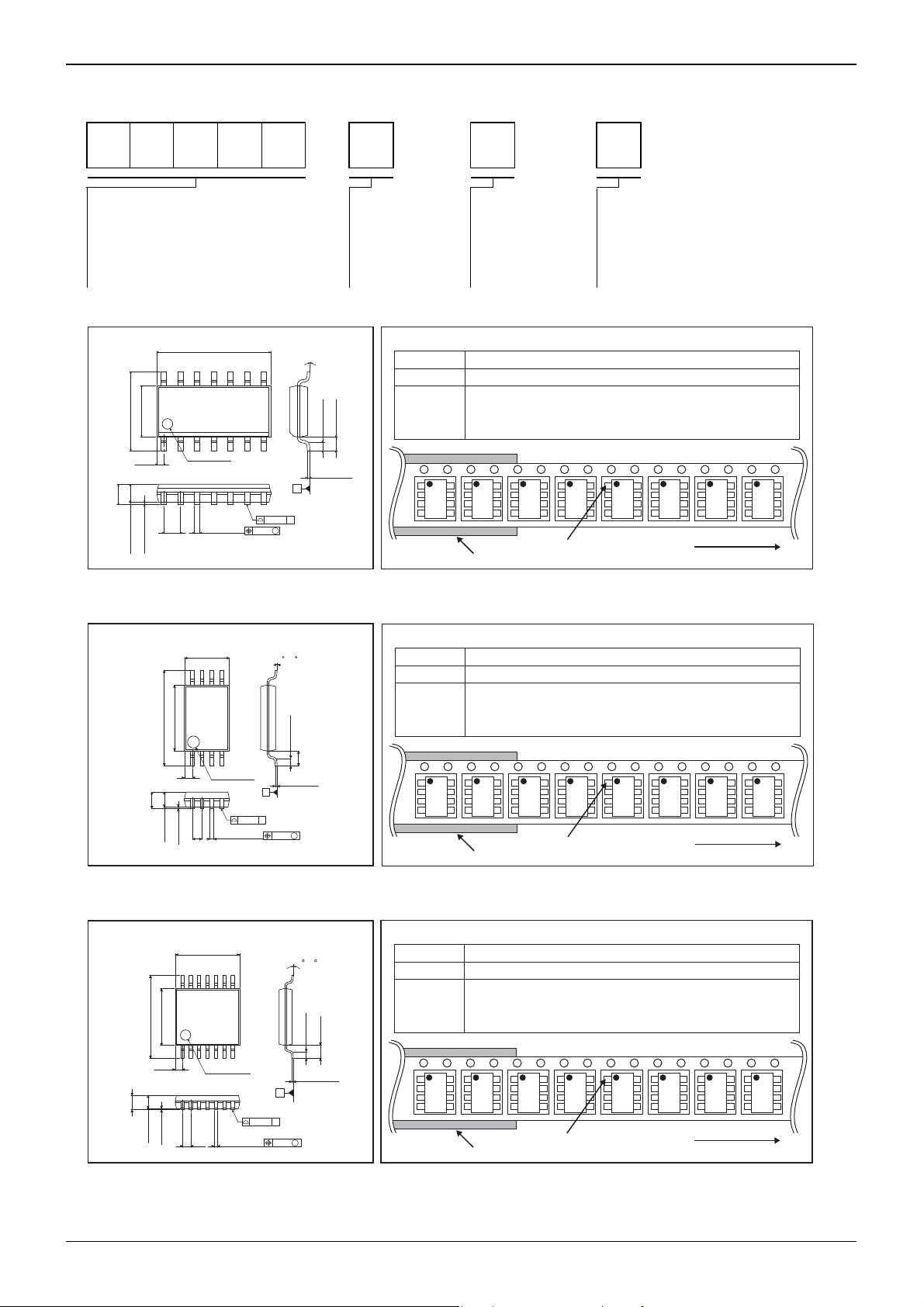
●Ordering part number
L M 3 3 9 W D T
Family name
LM393
LM339
LM2901
LM2903
S.O package14
8.65± 0.1
(Max 9.0 include BURR)
814
4°
ESD Tolerance
applicable
W : 2kV
None : Normal
+6°
−4°
Package type
D : S.O package
P : TSSOP
S : Mini SO
<Tape and Reel information>
Embossed carrier tapeTape
Quantity
2500pcs
Technical Note
Packaging and forming specification
T: Embossed tape and reel
6.0± 0.2
0.515
1.65MAX
1.375± 0.075
TSSOP8
3.9± 0.1
1PIN MARK
1.27
0.175± 0.075
3.0± 0.1
(MAX 3.35 include BURR)
8765
4.4± 0.1
6.4± 0.2
1
0.525
1.2MAX
1.0± 0.05
0.1± 0.05
0.65
+0.05
0.42
−0.04
234
1PIN MARK
0.245
0.08 S
+0.05
−0.04
0.08
71
0.08 S
S
M
0.08
4 ± 4
0.145
0.5± 0.15
M
S
+0.05
−0.03
1.05±0.2
0.65±0.15
+0.05
0.22
−0.03
(Unit : mm)
(Unit : mm)
1.0± 0.2
(Unit : mm)
Direction
of feed
The direction is the 1pin of product is at the upper left when you hold
()
reel on the left hand and you pull out the tape on the right hand
Reel
<Tape and Reel information>
Embossed carrier tapeTape
Quantity
Direction
of feed
2500pcs
The direction is the 1pin of product is at the upper left when you hold
()
reel on the left hand and you pull out the tape on the right hand
Reel
1pin
Order quantity needs to be multiple of the minimum quantity.
∗
1pin
Order quantity needs to be multiple of the minimum quantity.
∗
Direction of feed
Direction of feed
TSSOP14
5.0±0.1
(Max 5.35 include BURR)
14
4.4±0.1
6.4±0.2
1
0.55
1.2MAX
1.0±0.05
0.1±0.05
www.rohm.com
© 2011 ROHM Co., Ltd. All rights reserved.
1PIN MARK
0.65
0.245
8
7
S
0.08 S
+0.05
−0.04
0.08
±44
0.5±0.15
0.145
M
1.0±0.2
+0.05
−0.03
(Unit : mm)
<Tape and Reel information>
Embossed carrier tapeTape
Quantity
Direction
of feed
2500pcs
The direction is the 1pin of product is at the upper left when you hold
()
reel on the left hand and you pull out the tape on the right hand
Reel
16/17
1pin
Order quantity needs to be multiple of the minimum quantity.
∗
Direction of feed
2011.06 - Rev.C
Page 17

LM393DT,LM393PT,LM393ST,LM393WDT,LM393WPT,
LM2903DT,LM2903PT,LM339DT,LM339PT,LM2901DT,LM2901PT
Mini SO8
3.0± 0.1
(MAX 3.35 include BURR)
578
6
4 ± 4
<Tape and Reel information>
Quantity
Technical Note
Embossed carrier tapeTape
2500pcs
4.9± 0.2
1.1MAX
0.85±0.05
3.0± 0.1
1234
0.525
0.1±0.05
0.65
1PIN MARK
+0.05
0.32
−0.04
S
0.08 S
0.08
0.45± 0.15
0.145
M
0.95± 0.2
+0.05
−0.03
(Unit : mm)
Direction
of feed
The direction is the 1pin of product is at the upper left when you hold
()
reel on the left hand and you pull out the tape on the right hand
Direction of feed
Reel
1pin
Order quantity needs to be multiple of the minimum quantity.
∗
www.rohm.com
© 2011 ROHM Co., Ltd. All rights reserved.
17/17
2011.06 - Rev.C
Page 18
Notes
No copying or reproduction of this document, in par t or in whole, is permitted without the
consent of ROHM Co.,Ltd.
The content specied herein is subject to change for improvement without notice.
The content specied herein is for the purpose of introducing ROHM's products (hereinafter
"Products"). If you wish to use any such Product, please be sure to refer to the specications,
which can be obtained from ROHM upon request.
Examples of application circuits, circuit constants and any other information contained herein
illustrate the standard usage and operations of the Products. The peripheral conditions must
be taken into account when designing circuits for mass production.
Great care was taken in ensuring the accuracy of the information specied in this document.
However, should you incur any damage arising from any inaccuracy or misprint of such
information, ROHM shall bear no responsibility for such damage.
The technical information specied herein is intended only to show the typical functions of and
examples of application circuits for the Products. ROHM does not grant you, explicitly or
implicitly, any license to use or exercise intellectual property or other rights held by ROHM and
other parties. ROHM shall bear no responsibility whatsoever for any dispute arising from the
use of such technical information.
The Products specied in this document are intended to be used with general-use electronic
equipment or devices (such as audio visual equipment, ofce-automation equipment, communication devices, electronic appliances and amusement devices).
The Products specied in this document are not designed to be radiation tolerant.
While ROHM always makes efforts to enhance the quality and reliability of its Products, a
Product may fail or malfunction for a variety of reasons.
Please be sure to implement in your equipment using the Products safety measures to guard
against the possibility of physical injury, re or any other damage caused in the event of the
failure of any Product, such as derating, redundancy, re control and fail-safe designs. ROHM
shall bear no responsibility whatsoever for your use of any Product outside of the prescribed
scope or not in accordance with the instruction manual.
The Products are not designed or manufactured to be used with any equipment, device or
system which requires an extremely high level of reliability the failure or malfunction of which
may result in a direct threat to human life or create a risk of human injur y (such as a medical
instrument, transportation equipment, aerospace machiner y, nuclear-reactor controller, fuelcontroller or other safety device). ROHM shall bear no responsibility in any way for use of any
of the Products for the above special purposes. If a Product is intended to be used for any
such special purpose, please contact a ROHM sales representative before purchasing.
If you intend to export or ship overseas any Product or technology specied herein that may
be controlled under the Foreign Exchange and the Foreign Trade Law, you will be required to
obtain a license or permit under the Law.
Notice
www.rohm.com
© 2011 ROHM Co., Ltd. All rights reserved.
Thank you for your accessing to ROHM product informations.
More detail product informations and catalogs are available, please contact us.
ROHM Customer Support System
http://www.rohm.com/contact/
R1120
A
 Loading...